US7548675B2 - Optical cables for consumer electronics - Google Patents
Optical cables for consumer electronicsDownload PDFInfo
- Publication number
- US7548675B2 US7548675B2US11/198,619US19861905AUS7548675B2US 7548675 B2US7548675 B2US 7548675B2US 19861905 AUS19861905 AUS 19861905AUS 7548675 B2US7548675 B2US 7548675B2
- Authority
- US
- United States
- Prior art keywords
- digital
- interface
- optical
- electrical
- optical cable
- Prior art date
- Legal status (The legal status is an assumption and is not a legal conclusion. Google has not performed a legal analysis and makes no representation as to the accuracy of the status listed.)
- Expired - Lifetime
Links
Images


Classifications
- H—ELECTRICITY
- H04—ELECTRIC COMMUNICATION TECHNIQUE
- H04N—PICTORIAL COMMUNICATION, e.g. TELEVISION
- H04N7/00—Television systems
- H04N7/22—Adaptations for optical transmission
- G—PHYSICS
- G02—OPTICS
- G02B—OPTICAL ELEMENTS, SYSTEMS OR APPARATUS
- G02B6/00—Light guides; Structural details of arrangements comprising light guides and other optical elements, e.g. couplings
- G02B6/24—Coupling light guides
- G02B6/42—Coupling light guides with opto-electronic elements
- G02B6/4201—Packages, e.g. shape, construction, internal or external details
- G02B6/4246—Bidirectionally operating package structures
Definitions
- the present inventionrelates to optical communication between digital consumer electronics. More specifically, the present invention relates generally to video and audio data transmission cables and interfaces.
- Digital consumer electronicssuch as digital video displays, digital video disk (DVD) readers, flat screen computer monitors, high definition television (“HDTV”), digital plasma screens, digital audio readers, digital audio encoders and readers, digital audio amplifiers, and digital audio processing devices have become of increased popularity.
- HDTVhigh definition television
- digital plasma screensdigital audio readers, digital audio encoders and readers, digital audio amplifiers, and digital audio processing devices have become of increased popularity.
- DVIdigital video interface
- HDMIhigh definition multimedia interface
- HDMItransmission minimized differential signaling
- DVIis a display interface developed by the Digital Display Working Group (“DDWG”).
- the DVI specificationcan provide a high-speed digital connection between DVI digital source devices (e.g. DVI digital video processing devices) and DVI digital sink devices (e.g. DVI digital video display devices).
- DVI digital source devicese.g. DVI digital video processing devices
- DVI digital sink devicese.g. DVI digital video display devices
- One common implementation of DVIis as an interface for a computer having a video controller card and a digital display device (CRT, LCD, projector, etc) having a display controller.
- CTRdigital display device
- LCDliquid crystal display
- projectoretc
- DVIutilizes a high-speed serial interface and TMDS to send data to the DVI sink device.
- TMDSconveys data by transitioning between “on” and “off” states.
- An encoding algorithmuses Boolean exclusive OR (“XOR”) or exclusive NOR (“XNOR”) operations applied to minimize the transitions to avoid excessive electromagnetic interference (“EMI”) levels in the DVI cable. An additional operation is performed to balance the DC signal.
- XORexclusive OR
- XNORexclusive NOR
- the digital DVI connectorhas 24 pins that can accommodate up to two TMDS links.
- the basic TMDS transmission lineis made up of three data channels and a clock channel. Data comprises 8 bit pixels in each of three channels (R/G/B). In some instances, a pair of TMDS lines may be used to achieve higher data rates.
- the digital interfaceincludes a 5VDC power source, and a hot plug detect channel.
- the DVI-I combined digital and analog pin assignmentsare similar to the DVI-D digital only interface pin assignments, but further includes several pins for transmission of an analog signal.
- FIG. 1illustrates the typical flow of data from a graphics controller 120 of a DVI source device 125 , such as a digital video processing device, through the TMDS links 130 and to the display controller 135 of a DVI sink device 140 , such as a digital video display device.
- incoming 8-bit datais encoded into 10-bit transition-minimized, DC-balanced characters.
- the first eight bitsare encoded data, and the ninth bit identifies whether the data was encoded with XOR or XNOR logic; the tenth bit is used for DC balancing.
- DVI cables having copper electrical cablesmay be limited to a length of about 3-5 meters. This limited length reduces the number of potential applications that can utilize DVI cables. For example, the length limits remote placement of digital video components.
- DVI-data ratestypically range from 22.5 mega pixels per second (Mpps) to 165 Mpps (up to 1.65 Giga bits). Because TMDS conveys data by transitioning between “on” and “off” states, electromagnetic interference (“EMI”) levels in the DVI cable can also limit the speed at which data may be transferred.
- Mppsmega pixels per second
- EMIelectromagnetic interference
- DVIdigital video processors and digital video displays may be incompatible or incapable of interoperation with one another.
- bidirectional communication for reconfiguring a digital video processor and/or digital video displaywould be desirable.
- configuration datais typically not transmitted.
- many DVI interfaceslack sufficient connectivity to transmit data (e.g. configuration data) from the digital video display to the digital video processor. As a result, a digital video processor and a digital video display can remain incompatible.
- HDMIis backward compatible with PCs, displays, and consumer electronics devices incorporating the DVI standard.
- HDMIis based on the TMDS serial link technology.
- HDMI technologysupports standard, enhanced, or high-definition video, plus multi-channel digital audio on a single cable. It transmits ATSC HDTV standards and supports 8-channel digital audio with 5 Gbps of bandwidth.
- the HDMI technology, functionality, and hardwareis disclosed in the “High-Definition Multimedia Interface” specification Version 1.1, May 20, 2004, by HDMI Licensing, LLC, the contents of which is hereby expressly incorporated by reference herein in its entirety.
- the HDMI interfaceis provided for transmitting digital television audiovisual signals from DVD players, set-top boxes and other audiovisual source devices to HDMI sink devices, such as television sets, projectors and other audio visual devices.
- HDMIcan carry multi-channel audio data and can carry standard and high definition consumer electronics video formats. Content protection technology is also available. HDMI can also carry control and status information in both directions.
- HDMI block diagramis shown where a standard HDMI cable includes four differential pairs 201 - 204 that make up the TMDS data and clock channels, referred to collectively as HDMI TMDS links 200 . These data channels are used to carry video, audio and auxiliary data.
- HDMIcarries a VESA DDC channel 205 .
- the DDC channel 205is used for configuration and status exchange between a HDMI source 210 and a HDMI sink 215 .
- the optional CEC protocol line 220provides high-level control functions between all of the various audiovisual products in a user's environment.
- Audio, video and auxiliary datais transmitted across the three TMDS data channels 201 - 203 .
- Video pixel clock datais transmitted on the TMDS clock channel 204 and is used by an HDMI receiver 230 as a frequency reference for data recovery on the three TMDS data channels 201 - 203 .
- Video datais carried as a series of 24-bit pixels on the three TMDS data channels 201 - 203 .
- TMDS encodingconverts the 8 bits per channel into a 10 bit DC-balanced, transition minimized sequence which is then transmitted serially across the HDMI TMDS data channels 201 - 203 at a rate of 10 bits per pixel clock period.
- Video pixel ratescan range from 25 MHz to 165 MHz.
- the video pixelscan be encoded in either RGB, YCBCR 4:4:4 or YCBCR 4:2:2 formats.
- HDMIIn order to transmit audio and auxiliary data across the TMDS channels 200 , HDMI uses a packet structure. In order to attain higher reliability of audio and control data, this data is protected with an error correction code and is encoded using a special error reduction coding to produce the 10-bit word that is transmitted.
- HDMIcan carry a single such stream at sample rates up to 192 KHz or from two to four such streams (3 to 8 audio channels) at sample rates up to 96 KHz.
- HDMIcan also carry compressed (e.g. surround-sound) streams.
- the DDC channel 205is used by the HDMI source device 210 to read the HDMI sink device's 215 Enhanced Extended Display Identification Data (E-EDID) to discover the sink device's 215 configuration and/or capabilities.
- E-EDIDEnhanced Extended Display Identification Data
- the HDMI source device 210reads the sink device's 215 E-EDID and delivers only the audio and video formats that are supported by the sink device 215 .
- the HDMI sink device 215can detect InfoFrames and process the received audio and video data appropriately.
- a digital consumer device's external HDMI connectionis embodied by two specified HDMI connectors, Type A or Type B. These connectors can be attached directly to the device or can be attached via a cable adapter that is shipped with the device.
- the Type A connectorcarries all required HDMI signals, including a single TMDS link.
- the Type B connectoris slightly larger and carries a second TMDS link, which is necessary to support very high-resolution computer displays requiring dual link bandwidth.
- a passive cable adapter between Type A and Type B connectorsis specified.
- the CEC protocol line 220is optionally used for higher-level user functions such as automatic setup tasks or tasks typically associated with infrared remote control usage.
- the Type A connectorcarries only a single TMDS link and is therefore only permitted to carry signals up to 165 Mpps. To support signals greater than 165 Mpps, the dual-link capability of the Type B connector is used.
- the input stream to the HDMI source's transmitter 235 from the HDMI source's controller 240will contain video pixel, packet and control data.
- the packet datacan include of audio and auxiliary data and associated error correction codes. These data items are processed in a variety of ways and are presented to the HDMI source's transmitter 235 as either 2 bits of control data, 4 bits of packet data or 8 bits of video data per TMDS channel.
- the HDMI source controller 240encodes one of these data types or encodes a Guard Band character on any given clock cycle.
- the stream of TMDS characters produced by the transmitter 235is serialized for transmission on the TMDS data channels 201 - 203 .
- a repeaterwhich is a device with a retransmission function for extension or distribution of digital video and/or audio signals from cables such as DVI and HDMI cables.
- the circuitry of a repeatercan retrieve, equalize, amplify, and re-transmit the digital video and/or digital audio signals into another length of cable.
- a repeatermay be capable of transmitting digital video and/or audio signals to about 25 or 35 meters in some instances.
- repeatercan be quite expensive, add additional hardware and circuitry require additional cables for the extension, and even still be relatively limited in distances to which the repeater can transmit digital video and/or audio signals and bandwidth of the cables. Therefore, repeaters have not provided a desired solution to many of the problems currently experienced with these cables, but rather tried to mitigate the limitations of such cables.
- a digital optical cable for coupling a digital source device with a signal sink devicecan include an optical fiber having a first end and a second end.
- the digital optical cablecan also include a first interface configured to couple the digital source device to the first end of the optical fiber.
- the first interfacecan include an optical transmitter for receiving an electronic video signal from the digital source device, converting the electronic video signal to an optical signal, and for transmitting the optical signal onto the first end of the optical fiber.
- a second interfacecan be configured to couple the digital sink device to the second end of the optical fiber.
- the second interfacecan include an optical receiver for receiving the optical signal transmitted by the optical transmitter from the second end of the optical fiber, converting the optical signal to an electronic video signal, and transmitting the electronic signal to the digital sink device.
- a cable for bidirectional communication between a first digital consumer electronic device and a second digital consumer electronic devicecan include an optical fiber having a first end and a second end and a first interface coupled to the first end of the optical fiber.
- the first interfacecan include first electrical connections configured to receive electrical TMDS signals from a receptacle of the first digital consumer electronic device and means for converting at least one of the TMDS signals to an outgoing optical signal and for transmitting the outgoing optical signal onto the first end of the optical fiber.
- the cablecan further include a second interface.
- the second interfacecan include means for receiving the outgoing optical signal and for converting the outgoing optical signal back into the at least one of the TMDS signals and second electrical connections configured to transmit the electrical TMDS signals to a receptacle of the second digital electronic consumer device.
- FIG. 1illustrates the typical flow of data from the graphics controller of a DVI source to the display controller of a DVI sink device
- FIG. 2illustrates the typical flow of data from the graphics and audio controller of a HDMI source to the display and audio controller of a HDMI sink;
- FIG. 3illustrates a digital optical cable according to an example embodiment of the present invention
- FIG. 4illustrates a digital optical cable according to an example embodiment of the present invention
- FIG. 5illustrates a digital optical cable according to an example embodiment of the present invention
- FIG. 6illustrates a digital optical cable according to an example embodiment of the present invention
- FIG. 7illustrates a digital optical cable according to an example embodiment of the present invention
- FIG. 8Aillustrates a digital optical cable according to an example embodiment of the present invention
- FIG. 8Billustrates a bidirectional optical transceiver for use in a digital optical cable according to an example embodiment of the present invention
- FIG. 9illustrates a bidirectional optical transceiver for use in a digital optical cable according to an example embodiment of the present invention.
- FIG. 10illustrates a bidirectional optical transceiver for use in a digital optical cable according to an example embodiment of the present invention
- FIG. 11illustrates a bidirectional optical transceiver for use in a digital optical cable according to an example embodiment of the present invention
- FIG. 12illustrates a bidirectional optical transceiver for use in a digital optical cable according to an example embodiment of the present invention
- FIG. 13illustrates a bidirectional optical transceiver with an integrated monitor photodiode for use in a digital optical cable according to an example embodiment of the present invention
- FIGS. 14A and 14Billustrate a bidirectional optical transceiver with an integrated monitor photodiode for use in a digital optical cable according to an example embodiment of the present invention.
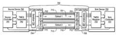
- the digital optical cable 300can comprise an optical fiber 301 having a first end 302 and a second end 303 .
- a first interface 304is coupled to the first end 302 of the optical fiber 301
- a second interface 305is coupled to the second end 303 of the optical fiber 301 .
- the first interface 304 of the digital optical cable 300is coupled to a digital source device 340 such as a DVI or HDMI digital video and/or audio processing device.
- the digital source device 340includes a source controller 341 and a TMDS transmitter 342 .
- the second interface 305 of the digital optical cable 300is coupled to a digital sink device 320 , such as a DVI or HDMI digital video display and/or audio output device.
- the digital sink device 320includes a TMDS receiver 322 and a sink controller 321 .
- the first interface 304 of the digital optical cable 300can include a serializer 306 , such as an electronic serializer circuit, and a means for converting an electrical signal to an optical signal, such as a transmit optical subassembly (“TOSA”) 307 .
- the serializer 306may be an electrical serializer circuit that receives the electrical TMDS signals (the number of TMDS signals depends on the standard) from the TMDS transmitter 342 and serializes the TMDS signals into a single electrical signal.
- the TOSA 307can include an optical transmitter, such as a light emitting diode (“LED”) or a laser diode (e.g. a VCSEL), that receives the electrical serialized data signal from the serializer 306 and converts the electrical serialized data signal into an optical serialized data signal for transmission onto the optical fiber 301 .
- LEDlight emitting diode
- VCSELlaser diode
- the second interface 305 of the digital optical cable 300includes a means for receiving the optical signal and converting the optical signal to an electrical signal, such as a receive optical subassembly (“ROSA”).
- the ROSA 308can include an optical receiver, such as a photodiode, that receives the optical serialized data signal from the optical fiber 301 and converts the optical serialized data signal to an electrical serialized data signal.
- a deserializer 309may be an electrical deserializer circuit that receives the electrical serialized data signal from the ROSA 308 and deserializes the electrical serialized data signal into TMDS signals (the number of TMDS signals will depend on the standard) for transmission to the TMDS receiver 322 of the digital sink device 320 .
- the digital source device 340e.g. a DVD player, digital cable box, or computer
- the first interface 304 of the digital optical cable 300is connected to the first interface 304 of the digital optical cable 300 .
- the second interface 305 of the digital optical cable 300is connected to the sink device 320 (e.g. a digital television, digital audio system, or a digital monitor).
- the source controller 341 of the digital source device 340transmits data signals, such as pixel data, audio data, and/or control data, to the TMDS transmitter 342 , which converts the data signals into the TMDS data signal format for a particular standard (e.g. DVI or HDMI).
- the TMDS transmitter 342transmits the TMDS data signals to the serializer 306 .
- the serializer 306receives the TMDS signals and serializes the TMDS signals into a single electrical serialized data signal.
- the serializer 306transmits the electrical serialized data signal to the TOSA 307 .
- the TOSA 307converts the electrical serialized data signal to an optical serialized data signal and transmits the optical serialized data signal to the optical fiber 301 .
- the optical serialized data signalis received by the ROSA 308 of the second interface 305 and the ROSA 308 converts the optical serialized data signal back to an electrical serialized data signal.
- the ROSA 308transmits the electrical serialized data signal to a deserializer 309 , which deserializes the electrical serialized data signal back into several TMDS signals depending on the standard used by the digital sink device 320 (e.g. DVI or HDMI).
- the deserializer 309transmits the TMDS signals to a TMDS receiver 322 located on the digital sink device 320 .
- the TMDS receiver 322converts the TMDS signals to video and/or audio data signals, such as pixel data, audio data, and/or control data, and the signals are output to the sink controller 321 of the digital sink device 320 .
- a digital optical cable 400is shown according to another example embodiment of the present invention.
- a first interface 404can include a plurality of TOSAs (or transmit chips) 406 and a wavelength-division multiplexer (“WDM”) 407 .
- Wavelength-division multiplexingcombines beams of light from different wavelengths into a single optical transmission to be received by an optical fiber.
- a second interface 405includes a wavelength-division demultiplexer (“WDD”) 408 and a plurality of ROSAs (or receiver chips) 409 .
- the WDD 408separates a multiplexed beam into separate beams of light of different wavelengths
- the digital source device 440is connected to the first interface 404 of the digital optical cable 400 .
- the second interface 405 of the digital optical cable 400is connected to the digital sink device 420 .
- the source controller 441 of the source device 440produces data signals, such pixel data, audio data, and/or control data.
- the data signalsare transmitted to the TMDS transmitter 442 , which converts the data signals into the TMDS data signal format (conforming to the applicable standard, e.g. DVI or HDMI).
- the TMDS transmitter 442transmits the TMDS data signals to the plurality of TOSAs 406 , one TOSA receiving each TMDS data signal.
- the TOSAs 406each include an optical transmitter, such as a laser or LED.
- Each TOSA 406transmitting light at a slightly shifted wavelength from the other TOSAs 406 .
- the TOSAs 406convert the electrical TMDS signals to optical signals and transmit the optical signals to the WDM 407 .
- the WDM 207receives the optical signals and combines the optical signals from the different transmitters (each at a different wavelength) into a multiplexed optical signal, and transmits the multiplexed optical signal onto a first end 402 of the optical fiber 401 .
- the multiplexed optical signalis received from the second end 403 of the optical fiber 401 by the WDD 408 of the second interface 405 .
- the WDD 408separates the individual wavelengths transmitted, and guides the separate optical TMDS signals to the appropriate one of the ROSAs 409 .
- Each of the ROSAs 409includes an optical receiver that converts the optical TMDS signals back to an electrical TMDS signal.
- the ROSAs 409transmit the electrical TMDS signals to a TMDS receiver 422 located on the sink device 420 .
- the TMDS receiver 422converts the TMDS signals to video display and/or audio data signals, such as pixel data, audio data, and control data, and the data is output to a display and/or audio system of the sink device 420 .
- a digital optical cable 500is shown according to another example embodiment of the present invention.
- the digital optical cable 500uses time-division multiplexing to transmit the TMDS signals across an optical fiber 501 having a first end 502 and a second end 503 .
- Time-division multiplexingis digital multiplexing in which two or more apparently simultaneous channels are derived from a single optical spectrum by interleaving pulses. Therefore each channel is allocated access to the optical transmission link in sequential intervals.
- a similar methodis a packet switched transmission which may be particularly advantageous in an HDMI optical cables.
- the first interface 504includes a time division multiplexer (“TDM”) 506 and a TOSA 507 .
- the second interface 505includes a ROSA 508 and a time division demultiplexer (“TDD”) 509 .
- the source controller 541 of the digital source device 540produces data signals (e.g. pixel, audio, and/or control data signals).
- the data signalsare transmitted to the TMDS transmitter 542 , which converts the data signals into the TMDS data signal format.
- the TMDS transmitter 542transmits the TMDS data signals to the TDM 506 .
- the TDM 506receives the TMDS signals and interleaves the signals for sequential transmission to the TOSA 507 .
- the TOSA 507receives the interleaved signals, converts the electrical signals transmitted from the TDM 507 into optical signals, and transmits the optical signals to the optical fiber 501 .
- the optical signalsare received by the ROSA 508 of the second interface 505 .
- the ROSA 508includes an optical receiver that converts the optical signals back to electrical signals and transmits the electrical signals to the TDD 509 .
- the TDD 509separates the received electrical signals transmitted into TMDS signals (e.g. based on a field), and transmits the separate TMDS signals to the TMDS receiver 522 located at the digital sink device 520 .
- the TMDS receiver 522converts the TMDS signals into video and/or audio data signals, and the data signals are output to the display and/or audio system of the digital sink device 520 .
- the digital optical/electrical cable 600comprises an optical fiber 601 having a first end 602 and a second end 603 , and an electrical link (e.g. a metal wire or cable) 610 having a first end 611 and second end 612 . Both the optical fiber 601 and the electric link 610 can be encased by a plastic covering 613 .
- a first interface 604is coupled to both the first end 602 of the optical fiber 601 and the first end 611 of the electrical link 610 .
- a second interface 605is coupled to both the second end 603 of the optical fiber 601 and the second end 612 of the electrical link 610 .
- the first interface 604 of the digital optical/electrical cable 600is coupled to a digital source device 640
- the second interface 605 of the digital optical/electrical cable 600is coupled to a digital sink device 620 .
- the TMDS signals from the TMDS transmitter 642 of the source device 640are serialized by the serializer 606 , transmitted by the TOSA 607 and received across the optical/electrical cable 600 by the ROSA 608 , deserialized by the deserializer 609 , and transmitted to the TMDS receiver 622 of the digital sink device 620 .
- the optical fiber 601can provide data signal transmission from the digital source device 640 to the digital sink device 620 in a similar fashion to that described above with reference to FIG. 3 .
- the electrical link 610electrically couples the sink controller 621 of the sink device 620 to the source controller 641 of the source device 640 .
- the electrical link 610can provide electrical communication for a return signal from the sink device 620 to the source device 640 in a direction opposite to that provided by the optical fiber 601 . Bidirectional communication allows for both the source device 640 and the sink device 620 to send and receive data with each other.
- the electrical link 610can also be used to provide unidirectional electrical communication or bidirectional electrical communication directions.
- the electrical link 610(or a plurality of electrical links) can provide electrical communication for transmission of the Display Data Channel and/or the CEC signals in a HDMI embodiment (e.g. see FIG. 2 ).
- the Display Data Channel and/or the CEC signalscan also be transmitted along with the TMDS signals according to any of the embodiments described herein.
- the optical fiber 601can be used to transfer the TMDS signals from the digital source device 640 to the digital sink device 620 , in a direction where a larger bandwidth and larger transfer rate may be most advantageous.
- the electrical link 610can be used to transfer a data signal in either direction in applications where the larger bandwidth and larger transfer rate may not be required.
- the electrical link 610may be used to send information that identifies the manufacturer and model number of the sink device 620 or the source device 640 . This information may then be displayed on a screen by the digital source device 640 or the digital sink device 620 .
- a relatively low bandwidthis needed to transmit information identifying the manufacturer and model number.
- Other low bandwidth signalscan include various handshaking, configuration, updating of firmware or software, or control signals.
- the electrical link 610can comprise more than one electrical wires or cables for transferring data between the sink device 620 to the source device 640 .
- the electrical link 610can be an unshielded twisted pair cable, ribbon cable, coaxial cable, etc.
- wavelength-division multiplexing and time-division multiplexingmay be implemented for communication across any of the optical fibers discussed herein in a similar fashion to that described above with reference to FIG. 4 and FIG. 5 .
- the electrical link 610may also transmit analog data signals between the sink device 620 and the source device 640 .
- TDMmay be used to transmit data over the electrical link 610 by interlacing packets of data in each direction with a header and fields or other means for identifying the source and/or purpose of the data in the packet payload.
- the digital optical cable 700comprises a first optical fiber 701 having a first end 702 and a second end 703 , and a second optical fiber 710 having a first end 711 and a second end 712 . Both the first optical fiber 701 and the second optical fiber 710 can be encased by a single plastic covering 713 .
- a first interface 704is coupled to both the first end 702 of the first optical fiber 701 and the first end 711 of the second optical fiber 710 .
- a second interface 705is coupled to both the second end 703 of the first optical fiber 701 and the second end 712 of the second optical fiber 710 .
- the first interface 704 of the digital optical cable 700is coupled to a digital source device 740
- the second interface 705 of the digital optical cable 700is coupled to a digital sink device 720
- the first optical fiber 701is used for transmission of the TMDS signals from the source device 740 to the sink device 720
- the optical fiber 701provides data signal transmission from the source device 740 to the sink device 720 in a similar fashion to that described above with reference to FIG. 3 .
- the second optical fiber 710can be used for a return data transmission in the opposite direction from the sink device 720 to the source device 740 .
- the second interface 705includes a TOSA 714 that receives an electrical return signal from the sink controller 721 of the sink device 720 .
- the TOSA 714converts the electrical return signal into an optical return signal and transmits the optical return signal onto the second end 712 of the second optical fiber 710 .
- the first interface 704includes a ROSA 715 that receives the optical return signal from the first end 711 of the second optical fiber 710 and converts the optical return signal into an electrical return signal.
- the ROSA 715transmits the electrical return signal to the source controller 741 of the source device 740 .
- the first optical fiber 701can be used to transfer the TMDS signals from the source device 740 to the sink device 720
- the second optical fiber 710can be used to transfer data in the opposite direction.
- This embodimentmay be particularly advantageous where a larger bandwidth and larger transfer rate is desirable in both directions. It should be appreciated that the direction of data transfer can be reversed or bidirectional in any of the embodiments described herein where advantageous.
- the TOSA 707 of the first interface 704can include a VCSEL for transmission of the optical serialized data signal onto the first optical fiber 701 ; and the TOSA 714 of the second interface 705 can include a LED for transmission of the return optical signal onto the second optical fiber 710 .
- An LEDmay be used for the TOSA 714 of the second interface 705 when lower bandwidths are acceptable. Using an LED may also be more cost efficient than using a VCSEL. Thus, a VCSEL may be used for higher bandwidth paths, such as those sending video and/or audio data, while an LED may be used for lower bandwidth paths, such as those sending manufacturer, configuration, and model information and/or control signals.
- WDM and TDMcan be implemented in either direction of the embodiment illustrated in FIG. 7 for communication across the optical fibers such as described above with reference to FIGS. 4 and 5 .
- the digital optical cablecan comprise a single optical fiber 801 having a first end 802 and a second end 803 , the optical fiber 801 .
- a first interface 804is coupled to the first end 802 of the optical fiber 801 and a second interface 805 is coupled to the second end 803 of the optical fiber 801 .
- the first interface 804 of the digital optical cable 800is coupled to a digital source device 840 (e.g. a DVI or HDMI source device), and the second interface 805 of the digital optical cable 800 is coupled to a sink device 820 (e.g. a DVI or HDMI source device).
- the same optical fiber 801is used for data transmission from the source device 840 to the sink device 820 , and for the transmission of a return signal in the opposite direction from the sink device 820 to the source device 840 .
- Each interface 804 and 805can include a fiber optic transceiver 807 for bidirectional optical communication.
- a transceivercan be both a means for converting an electrical signal to an optical signal, and also a means for converting an optical signal to an electrical signal.
- FIG. 8Bdepicts an example embodiment of a transceiver 807 .
- the transceiver 807can include a TOSA 810 for sending optical signals, and a ROSA 811 for receiving optical signals.
- the TOSA 810can include an optical transmitter (e.g. a laser or LED) that receives an electrical data signal, converts the electrical data signal into an optical data signal, and transmits the optical data signal onto the optical fiber 801 .
- the ROSA 811includes an optical receiver that receives an optical data signal from the optical fiber 801 and converts the signal to an electrical data signal.
- the transceiver 807can further include an optical circulator 812 that separates transmitted and received data signals. While a particular embodiment of a transceiver 807 is shown and described, other embodiments including other optical subassemblies and components can be used to send and receive optical signals over the digital optical cable, for example as discussed below with reference to FIGS. 9-14B .
- the TOSA 810 of the first interface 804can include a VCSEL for transmission of the optical serialized data signal onto the optical fiber 801 ; and the TOSA 810 of the second interface 805 can include a LED for transmission of the return optical signal onto the optical fiber 801 in the opposite direction.
- the optical cable 800couples the sink controller 821 of the sink device 820 to the source controller 841 of the source device 840 for bidirectional transmission of data.
- the optical fiber 801can be used to transfer the TMDS signals from the digital source device 840 to the digital sink device 820 .
- the same optical fiber 801can also be used to transfer return data in the opposite direction.
- the same optical fiber 801can be used to transfer the DDC and CEC signals. This embodiment may be particularly advantageous where a single optical fiber is desirable.
- WDM and TDMmay be implemented in either direction for communication across the optical fiber 801 .
- the highest speed communicationmay only be necessary in one direction (i.e. from the source device 840 to the sink device 820 ), but not necessarily in the opposite return direction.
- TDM across the single optical fiber 801may not be as advantageous because of asymmetric rates of data transfer, whereas WDM may be more advantageous.
- Power for the fiber optic componentscan be supplied by the 5VDC power source connection located on standard cables (e.g. DVI and HDMI cables). Power for the fiber optic components may also be supplied externally, or internally, to the fiber optic components from other exterior power sources or internal power sources.
- Fiber optic data transmissionis accurate and efficient over relatively long distances that may be many times longer than that typically achieved using metal based cables to transmit TMDS signals. Fiber optic data transmission over longer distances may also be less susceptible to interference than transmission using metal based cables. Fiber optic cables may also be thinner and lighter than metal cables. Fiber optic cables may also eliminate the need for digital to analog and analog to digital conversion. Therefore, the present invention may allow for increased length of digital, video, and/or audio cables, remote placement of digital video and/or audio components, reduced hardware, and less transmission errors over that available using conventional cables using copper links.
- fiber optic technologyis characterized by high bandwidth and reliable, high-speed data transmission. While a typical copper based cable bandwidth may range from 22.5 Mpps to 165 Mpps, reliable fiber optic communication over a single optical fiber may be able to achieve speeds faster than the speed of a copper based digital transmission cable.
- digital optical cables configured in accordance with the present inventionmay facilitate increased bandwidth and data transfer rates over copper based digital cables. The increased bandwidth and data transfer rates in turn may facilitate the use of higher resolution or larger displays having more display pixels.
- Embodiments of the present inventioncan comprise a TOSA including an optical package (e.g. a TO-Can package) having an optical transmitter (e.g. a VCSEL), a monitor photodiode, and a laser driver within the optical package for transmitting the optical signal to the optical fiber.
- an optical packagee.g. a TO-Can package
- an optical transmittere.g. a VCSEL
- monitor photodiodee.g. a VCSEL
- a laser drivere.g. a laser driver within the optical package for transmitting the optical signal to the optical fiber.
- the optical transmittere.g. a VCSEL
- monitor photodiodee.g. VCSEL
- laser drivere.g. a laser driver within the optical package for transmitting the optical signal to the optical fiber.
- the laser drivercan be a modulation laser driver for providing a modulation current source to the laser.
- a bias current sourcemay be supplied to the laser from a source external to the TOSA, such as the 5VDC power source connection located on a standard cable.
- the TO-Can packagecan be incorporated as part of the first interface and/or the second interface where a TOSA is referenced in the embodiments described above.
- Embodiments of the present invention implementing bidirectional optical communicationcan comprise various transceiver designs.
- the transceiver 807can comprise various different subcomponents, assemblies, and configurations for sending and receiving optical signals across the single optical fiber.
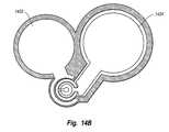
- FIG. 9a bidirectional optical assembly 910 is illustrated according to an example embodiment of the present invention.
- the bidirectional optical assembly 910can be used in the digital optical cable of FIG. 8 in place of the transceiver embodiment shown in FIG. 8A for bidirectional optical communication across the optical fiber 801 .
- FIG. 9is a basic diagram of a bidirectional multiband optical assembly 910 .
- Light 911 of a first wavelengthmay be emitted by light source 917 , which may be reflected at points 915 and 914 and exit optical port 913 .
- Light source 917may be a VCSEL outputting light 911 that may be modulated in one form or another with communication signals or the like. These functions may be accomplished with an electronics module 966 that is connected to source 917 .
- Source 917may be another kind of device as appropriate for an application of the assembly.
- Light 911may have other wavelengths, besides the first wavelength, which may be filtered out by a filter or mirror.
- Points 915 and 914are where light is reflected and may be located at mirrors that are discrete or integrated parts of structure 916 , such as an internal reflecting surface in the structure, or a reflective filter. Point 914 may be where filter 918 is reflective of a particular wavelength. Filter 918 may allow light 919 to pass through it to optical port 913 . Light 912 may enter optical port 913 and go through a wavelength filter 918 . Filter 918 may be a dichroic filter that reflects one or more wavelengths and transmits others. Filter 918 may be designed to pass light 919 of a second wavelength. All other wavelengths of light 912 are not transmitted through filter 918 . Light 919 of the second wavelength may be detected by a detector 921 and converted into electrical signals.
- Light 919may be modulated.
- Detector 921along with an electronics module 967 may demodulate such light.
- Detector 921may be a photo detector or another kind of device as appropriate for an application of the assembly.
- Light signalsmay be sent and received by device 910 simultaneously.
- components 917 and 921may both be detectors or sources and receive or send, respectively, various signals simultaneously on different wavelengths of light, or on the same wavelength.
- Device 917 and/or 921may both a source and a detector.
- Source 917 and detector 921may be enclosed within a standard TO can (e.g., TO-5 or TO-18) as optical components. These components may electronically and packaging-wise have interfaces to standard PCBs for small for factor pluggable (SFP) modules. These components may have other forms of packaging.
- source 917 and detector 921may be integral parts of structure 916 .
- Lenses 922 and 923 for light source 917 and detector 921respectively, may be molded plastic parts. The lenses also may be parts integrated into structure 916 or be molded as part of the structure. Lenses 922 and 923 may instead be part of TO can components 917 and 921 , or be situated on or monolithically be a part of the laser and detector chips.
- Lens 924 at optical port 913may focus incoming light to a mirror, filter or detector in structure 916 . It may also focus outgoing light to a light waveguide, such as a fiber, at optical port 913 . Lens 924 may have the same structural characteristics as those of lenses 922 and 923 . Lenses 922 , 923 and 924 may also be used to collimate light.
- Structure 916may be a molded plastic part, made from a material such as Ultem R , or it may be an injection molded metal part or other metal housing. Structure 916 also may be made from a composite material.
- the TO can optical components 917 and 921may be attached to the plastic or metal structure 916 with an epoxy or laser welding, respectively. These components are alignment tolerant.
- Metal ringsmay be attached to a plastic structure 916 for laser welding metal components to it.
- Dichroic filter 918 or mirrormay be placed in a molded indent formed within plastic or metal structure 916 and glued in place or it may be inserted and held in place by compression. A molded groove in structure 916 may provide appropriate alignment of dichroic filter 918 .
- structure 916may be composed of two pieces glued together, one or both of which may have dichroic reflectors deposited on their surfaces.
- FIG. 10shows a bidirectional optical device 1030 having a multitude of optical components, such as detectors or sources, or a mix of detectors and sources.
- the number of optical componentsis arbitrary, and may be determined by the application of device 1030 or the standard of a digital optical cable (e.g. the number of communication links in a DVI or HDMI standard).
- Device 1030reveals five optical components 1041 , 1042 , 1043 , 1044 and 1045 , as an illustrative example of a structure 1035 .
- Light 1036may arrive through port 1013 and light 1037 may exit port 1013 .
- Light 1036 receivedmay have a multitude of wavelengths (e.g. each representing a TMDS signal), each wavelength having communication signals different from those of other wavelengths.
- light 1037 sent outmay have a multitude of wavelengths (e.g. representing TMDS, or other, signals), each wavelength having communication signals different from those of other wavelengths.
- Light 1036 and light 1037may be conveyed to and from optical components 1041 , 1042 , 1043 , 1044 and 1045 by an optical mechanism 1038 .
- Mechanism 1038may be a light waveguide, an optical fiber, a series of mirrors, or other items to accomplish the conveyance of light 1036 and 1037 to and from the optical components. Or mechanism 1038 might not be utilized.
- Lenses 1024 and 1068may be used to focus or collimate light as appropriate. The lenses may be an integral part of structure 1035 .
- Light 1036 and light 1037 to or from optical components 1041 , 1042 , 1043 , 1044 and 1045may go through filters, for example, filters 1046 , 1047 , 1048 , 1049 and 1050 , respectively.
- filters 1046 , 1047 , 1048 , 1049 and 1050respectively.
- each optical componenthas a wavelength different from the other optical components, there may be a filter of that wavelength associated with the respective component.
- optical component 1041may send or receive light signals if a first wavelength or bandwidth (e.g. a first TMDS signal);
- optical component 1042may send or receive light signals of a second wavelength or bandwidth (e.g. a second TMDS signal);
- optical component 1043may send or receive light signals of a third wavelength or bandwidth (e.g.
- optical component 1044may send or receive light signals of a fourth wavelength or bandwidth (e.g. a fourth TMDS signal); and optical component 1045 may send or receive light signals of a fifth wavelength or bandwidth (e.g. a fifth TMDS signal).
- filter 1046may transmit or pass light signals only of a first wavelength or bandwidth; filter 1047 may transmit light only of a second wavelength or bandwidth; filter 1047 may transmit light only of a second wavelength or bandwidth; filter 1048 may transmit light of only a third wavelength or bandwidth; filter 1049 may transmit light of only a fourth wavelength or bandwidth; and filter 1050 may transmit light of only a fifth wavelength or bandwidth. All of optical components 1041 , 1042 , 1043 , 1044 and 1045 may send light signals 1037 and/or receive light signals 1036 at the same time.
- Filters 1046 , 1047 , 1048 , 1049 and 1050may be replaced with, for example, dichroic reflectors or other wavelength or bandwidth discriminating mechanisms. With such replacements, the optics may be adjusted for conveying light signals 1036 and 1037 to and from optical components 1041 , 1042 , 1043 , 1044 and 1045 .
- Structure 1035may be made from molded plastic, for example, Ultem R , metal, composite materials or other suitable materials. Structure 1035 may have similar features as those of structures 1010 and 1020 in FIGS. 1 and 2 .
- FIG. 11is a cross-sectional side view of an illustrative optical transceiver in accordance with the present invention.
- the illustrative optical transceiveris generally shown at 1140 , and includes an optical detector 1142 situated above an optical transmitter 1144 , both aligned along a common optical axis 1146 .
- the optical detector 1142preferably absorbs a first wavelength and/or range of wavelengths, while passing a a second wavelength and/or range of wavelengths.
- the optical transmitter 1144preferably transmits a second wavelength and/or range of wavelengths, which passes through the optical detector 1142 and out the top of the optical transceiver 1140 .
- both the incoming light beam and the outgoing light beampass through the top side of the optical transceiver 1140 .
- the optical transmitter 1144 shown in FIG. 11is a planar, current-guided GaAs/AlGaAs top emitting Vertical Cavity Surface Emitting Laser (VSCEL).
- the illustrative VCSEL 1144is formed on an n-doped gallium arsenide (GaAs) substrate 1148 , which has an n-contact layer 1150 provided on the bottom surface.
- An n-type mirror stack 1152is formed on the substrate 1148 .
- the n-type mirror stack 1152is preferably a distributed Bragg reflector (DBR), which includes periodic layers of doped AlGaAs with alternating higher and lower aluminum fractions.
- DBRdistributed Bragg reflector
- An active region 1154is shown atop the n-type mirror stack 1152 .
- the active region 1154preferably has a number of quantum wells, but may be any suitable active region as desired. Also, the active region 1154 may include a bottom confinement layer and a top confinement layer.
- a p-type mirror stack 1160is provided on top of the active region 1154 to complete the VCSEL structure.
- the p-type mirror stack 1160is preferably a distributed Bragg reflector (DBR), which includes periodic layers of doped AlGaAs with alternating higher and lower aluminum fractions.
- DBRdistributed Bragg reflector
- the n-type mirror stack 1152 , active region 1154 and p-type mirror stack 1160are preferably configured to produce an outgoing light beam that has the second wavelength and/or range of wavelengths.
- An optical detector 1142is provided atop the VCSEL 1144 .
- the illustrative optical detector 1142includes three series connected photodiodes, which are also connected in series with the VCSEL 1144 .
- a heavily p-doped buffer layer 1164may be provided on top of the top mirror 1160 , as shown.
- a p-doped layer 1166is provided on the heavily p-doped buffer layer 1164 , followed by an n-doped layer 1168 .
- Both the p-doped layer 1166 and the n-doped layer 1168may be AlGaAs.
- the Al fractionis preferably adjusted to tune the bandgap of the layers to achieve a desired absorption cutoff wavelength, which in the illustrative embodiment, is below the emission wavelength of the VCSEL 1144 .
- a reverse biased tunnel junction 1170is coupled to the first photodiode.
- the tunnel junction 1170includes two highly but oppositely doped adjacent layers to create an abrupt junction that produces a narrow depletion, allowing substantial tunneling current even at relative low reverse bias voltages.
- the bottom layer of the tunnel junction 1170is n-type and the top layer is p-type.
- the n-type bottom layermakes good electrical contact with the n-doped layer 1168 of the first photodiode
- the p-type top layermakes good electrical contact with a p-doped layer 1172 of the second photodiode, which includes P-doped layer 1172 and n doped layer 1174 .
- the tunnel junction 1170is formed, the p-doped layer 1172 is provided, followed by an n-doped layer 1174 to form the second photodiode.
- the tunnel junction 1170makes the series connection between the first photodiode and the second photodiode.
- both the p-doped layer 1172 and the n-doped layer 1174may be AlGaAs.
- the AI fractionis preferably adjusted to tune the bandgap of the layers to achieve the same cutoff wavelength as the first photodiode, but this is not required in all embodiments.
- Yet another tunnel junction 1176is then formed, followed by a p-doped layer 1178 and an n-doped layer 1180 to form a third photodiode.
- an incoming light beam 1184 having a first wavelength and/or range of wavelengthsis provided to the top of the optical transceiver 1140 .
- Each of the first, second and third photodiodesis preferably tuned to absorb at least a portion of the first wavelength and/or range of wavelengths of the incoming light beam 1184 .
- the p-type mirror stack 1160 of the VCSELis preferably at least partially reflective at the first wavelength and/or range of wavelengths. Thus, at least part of the light that is not absorbed by the first, second and third photodiodes will be reflected back through the photodiodes, as shown at 1186 .
- the thickness of the first, second and third photodiodesis preferably adjusted so that each photodiode absorbs approximately the same energy from the incoming light beams 1184 and 1186 .
- the thickness of the first-, second- and third-photodiodesis about 0.30, 0.27, and 0.23 microns, respectively, for an absorption wavelength of 808 microns.
- An upper contact layer 1182may be provided to make electrical contact to the n-type layer 1180 of the third photodiode.
- One or more quarter wave oxide or nitride layersmay also be provided on top of the structure 1140 to reduce reflection and to help protect the optical transceiver 1140 .
- one or more trenches 1196 a - 1196 dmay be etched through the first, second and third photodiodes, and in some embodiments, into the top p-type mirror stack 1160 of the VCSEL 1144 . This may be accomplished with a Reactive Ion Etch (RIE), but any suitable patterning method may be used.
- RIEReactive Ion Etch
- one or more of the periodic layers of the top p-type DBR mirror stack 1160 of the VCSEL 1144is provided with a higher A 1 concentration relative to the other periodic layers.
- layer 1190When exposed to an oxidizing environment through the one or more trenches 1196 a - 1196 d , layer 1190 is selectively oxidized in a lateral direction to form a current aperture 1192 for the VCSEL 1144 .
- the extent of the lateral oxidizationcan be controlled by controlling the exposure time of layer 1190 to the oxidizing environment. As can be seen, the exposure time is preferably controlled so that a desired current aperture 1192 remains.
- the current aperture 1192 of the VCSEL 1144has a diameter of about 5-10 microns.
- the lateral dimension of the first, second and third photodiodesis greater than the lateral dimensions of the aperture 1192 of the VCSEL 1144 .
- the lateral dimension of the first-, second- and third-photodiodesmay be on the order of 100-200 microns, while the lateral dimension of the optical cavity of the VCSEL 1144 may be on the order of 5-10 microns.
- the lateral dimension of the first-, second- and third-photodiodesmay be sufficiently wide to absorb much of the incoming light beam without the need for a lens or other light concentrating element.
- the alignment of the optical fiber to the first, second and third photodiodesmay not be difficult or critical.
- the aperture 1192 of the VCSEL 1144is relatively small relative to the diameter of the optical fiber, much of an outgoing light beam 1193 produced by the VCSEL 1144 will be captured by the optical fiber without the need for a lens or other light concentrating element. As such, an efficient and cost effective optical transceiver 1140 may be provided.
- the depth of the trenches 11196 a - 1196 dmay only be about 1-2 microns wide.
- a metal layermay then be deposited on top of the structure 1140 to fill in at least some of the trenches, such as trenches 1196 a and 1196 d , to make an electrical connection to the top mirror 1160 of the VCSEL 1144 .
- those trenches that are filled with the metal layermay first be lined with a dielectric layer as shown at 1195 a and 1195 d . As further described below, these electrical connections may be useful when it is desirable to provide the entire electrical potential produced by the series connected first, second and third photodiodes to other devices or structures.
- FIG. 12is a top view of the illustrative optical transceiver of FIG. 11 .
- FIG. 12shows the top of the optical detector 1142 including trenches 1196 a - 1196 d , as well as the lateral extent of the lateral oxidization of layer 1190 of VCSEL 1144 . Also shown is a metal contact used to make electrical contact to the top of the optical detector 1142 .
- the outer boundary of the illustrative optical detector 1142is defined by the outer trench, which is collectively shown at 1196 a and 1196 d .
- the outer trenchhelps electrically isolate the optical detector 1142 from other optical detectors or devices formed on the same substrate.
- the outer trenchalso helps keep the total capacitance of the optical detector 1142 down.
- the illustrative outer trench 1196 a and 1196 dis circular in shape, but other shapes may be used.
- the inner trench, collectively 1196 b 1196 cis also circular in shape, and is spaced inward from the outer trench.
- the inner trenchmay be filled with an oxide or other dielectric, if desired.
- the inner trench 1196 b and 1196 cinclude one or more bridges, such as bridges 1110 a - 1110 d .
- Bridges 1110 a - 1110 dprovide an electrical connection between the portion of the optical detector 1142 that is situated inside of the inner trench 1196 b and 1196 c and the portion of the optical detector 1140 that is situated between the inner trench 1196 b and 1196 c and the outer trench 1196 a and 1196 d .
- the metal contact 1104may only extend over and make an electrical connection to the portion of the optical detector 1142 situated between the inner trench 1196 b and 1196 c and the outer trench 1196 a and 1196 d .
- a metal tracemay be provided across the inner trench 1196 b and 1196 c to make an electrical connection to the portion of the optical detector 1142 situated inside of the inner trench 1196 b and 1196 c , if desired.
- the optical detector 1142may cover a relatively larger area than the aperture 1192 of the VCSEL 1144 .
- the extent of the lateral oxidizationis shown by dashed lines 1102 and 1108 .
- layer 1190 of VCSEL 1144is oxidized outward from the outer trench to dashed line 1102 and inward from the outer trench toward the inner trench.
- layer 1190 of VCSEL 1144is oxidized outward from the inner trench toward the outer trench, and inward from the inner trench to dashed line 1108 .
- Dashed line 1108outlines the current aperture 1192 of the VCSEL 1144 .
- the current aperture 1192has a diameter of about 5-10 microns, which produces a lower power VCSEL transmitter.
- the inner and outer trenchesmay be filled with an oxide or other isolation material.
- a metal layer(not shown in FIG. 12 ) may be deposited down into at least part of the some of the trenches, such as the inner and/or outer trenches 1196 a - 1196 d , to make an electrical connection to the top mirror 1160 of the VCSEL 1144 .
- a dielectric layermay first be provided to help prevent the metal layer from making electrical contact with the various intermediate layers of the optical detector 1142 .
- this electrical connectionmay be useful when it is desirable to make the entire electrical potential produced by the series connected first, second and third photodiodes available to other devices or structures.
- appropriate trenches and metal contactscan be provided such that all three electrical contacts are separately available on the top surface, enabling, for example, flip-chip bonding to either opaque or transparent substrates.
- any of the embodiments of the present invention illustrated hereincan include monolithically formed laser diodes and photodiodes.
- the laser diodes and photodiodesare connected through tunnel junctions such that a single power supply may be used to power the laser diodes and photodiodes.
- Appropriate contactsare formed to allow access to the various junctions of the laser diodes, tunnel junctions, and photodiodes.
- FIG. 13an example of an optoelectronic device including an epitaxial structure 1300 that includes layers formed on a wafer substrate is shown.
- the structure 1300is grown using a GaAs wafer.
- III-V (three-five) semiconductor combinationsmay also be used.
- FIG. 13shows a VCSEL 1301 .
- the VCSEL 1301 in the example shownincludes a top mirror 1302 , an active region 1304 , and a bottom mirror 1306 .
- a PN junctionexists in the active region 1304 .
- a spacer layer 1311is formed below the bottom mirror 1306 .
- the spacer layer 1311is preferably about 5 ⁇ /4 or 7 ⁇ /4 where ⁇ is the wavelength of light that the VCSEL 1301 is designed to emit.
- the spacer layer 1311may be any odd integral multiple of the wavelength (i.e.,
- nis an integer
- the spacer layer 1311must be sufficiently thick such that when etching is done to the spacer layer 1311 the deepest non-uniformities do not go all the way through the spacer layer 1311 and the shallowest potions reach the spacer layer 1311 . The goal, therefore is to expose the spacer layer 1311 without going all the way through the spacer layer 1311 at any point. Subsequent processing uses a selective etchant such as dilute hydrofluoric acid to uniformly expose the layer underlying the spacer.
- a selective etchantsuch as dilute hydrofluoric acid
- the epitaxial structure 1300further includes a tunnel junction 1308 , formed on and electrically connected to the VCSEL 1301 .
- the tunnel junction 1308includes a heavily doped n+ layer 1310 and a heavily doped p+ layer 1312 .
- the epitaxial structure 1300further includes a photodiode, formed on and electrically connected to the tunnel junction 1308 , which includes a second PN junction that is comprised of the heavily doped p+ type layer 1312 of the tunnel junction 1308 and a lightly doped photodiode n type layer 1314 .
- An additional p type layer(not shown) that is not as heavily doped may also be fabricated between the p+ type layer 1312 and the photodiode n type layer 1314 .
- the epitaxial structure 1300is constructed on an n type substrate 1316 . Although the substrate 1316 is shown in FIG.
- the substrateis actually in one embodiment of the invention in the hundreds of microns whereas the epitaxial structure including the photodiode, the tunnel junction 1308 , and the laser diode 1301 is about 10 microns.
- the epitaxial structure 1300is generally grown using a metal organic chemical vapor phase deposition (MOCVD) process.
- MOCVDmetal organic chemical vapor phase deposition
- the top mirror 1302is a distributed Bragg reflector (DBR) that generally comprises a number of alternating layers with high and low indexes of refraction. This creates a mirror with high reflectivity, around 99.5%.
- the top mirroris constructed of p type materials such as carbon doped aluminum gallium arsenide (AlGaAs), where the fraction of Al can vary from 0% to 100%.
- AlGaAscarbon doped aluminum gallium arsenide
- the top mirror 1302includes about 20 mirror periods where each period includes a high index of refraction layer and a low index of refraction layer.
- the active region 1304includes a number of quantum wells for stimulating the emission of laser energy. In the embodiment shown, active region 1304 is less than 1 micron.
- the bottom mirroris comprised of about 30 to 35 doped n type mirror periods. Silicon is one example of a dopant that may be used in the bottom mirrors.
- the tunnel junction 1308includes a heavily doped n+ layer 1310 and a heavily doped p+ layer 1312 .
- a heavily doped n+ layer 1310includes both layers of GaAs and InGaAs (e.g. several alternating layers) to tailor the bandgap and doping properties to improve the tunnel junction 1308 .
- the tunnel junction 1308be somewhat transparent so as to allow optical energy to pass through to the photodiode layer 1314 . This may be done in one embodiment by increasing doping on the heavily doped n+ layer 1310 so as to increase transparency through the so-called Burstein shift.
- the heavily doped p+ layer 1312is about 50 to 100 nanometers and preferably at least 3 ⁇ 10 19 of p type material (e.g., when used in an 850 nm laser).
- the heavily doped n+ layermay be nearly any practicable thickness without imposing an optical penalty.
- the photodiode 1318should be constructed so as to have an appropriate responsivity to incoming light.
- the photodiode 1318includes a lightly doped n layer 1314 that is approximately three microns or less when the VCSEL 1301 is designed to emit an 850 nm wavelength.
- One embodiment of the inventionincludes a lightly doped n layer 1314 that is about 1.5 microns.
- the thickness of the lightly doped n layer 1314can be used to tailor the responsivity and speed of the photodiode.
- contacts and oxide layersare formed through a photolithographic process.
- the formation of contactsallows appropriate biasing to be applied to, and signals to be read from the VCSEL 1301 and photodiode 1318 .
- the lithographic processincludes a series of acts where photoresist is applied to the epitaxial layers 1300 .
- the photoresistis then exposed lithographically to various patterns. Lithographic exposure allows a pattern of photoresist to remain on the epitaxial layers 1300 while the remainder of the photoresist may be washed from the epitaxial layers 1300 .
- the patterns of photoresist that remain on the epitaxial layers 1300block ions from being implanted in the epitaxial layers 1300 , metal from being deposited on the epitaxial layers 1300 , and etching solutions from etching portions of the epitaxial layers 1300 .
- a monolithic structure 1400that includes a VCSEL 1301 , a tunnel junction 1308 and a photodiode 1318 may be constructed with appropriate contacts and with appropriate isolation from other devices on a wafer being fabricated simultaneously.
- a tunnel junction contact 1422is formed such that it connects to the heavily doped p layer 1312 .
- a VCSEL contact 1424is formed such that it connects to the top mirror 1302 of the VCSEL 1301 .
- Another contactmay be formed on the bottom of the substrate 1316 to provide the appropriate contact to the photodiode 1318 .
- Isolation barriers 1426are formed to isolate the VCSEL 1301 and the photodiode 1318 from other devices being formed on the substrate 1316 .
- An aperture 1428is oxidized into the top mirror 1302 . The aperture 1428 is used primarily to direct current flow through the VCSEL 1301 .
- the optoelectronic device 1400is fabricated from an epitaxial structure 1300 .
- the epitaxial structure 1300has a dielectric such as silicon dioxide or silicon nitride grown on it to form a portion of the dielectric layer 1430 .
- a shallow trench maskis used to remove portions of the oxide using an etching process.
- An etch processis used to form the shallow trench 1432 in the VCSEL 1301 .
- the aperture 1428can then be oxidized into the VCSEL 1301 .
- a deep trench maskcan then be used to etch the deep trench 1434 .
- An etchcan be used to etch down to a thick AlAs spacer 1311 .
- This spacermay be AlAs or another AlGaAs composition, so long as the fraction of aluminum is substantially greater than that in the underlying layer.
- a stop etchmay be used to etch through the AlAs spacer 1311 to the n+ layer 1310 .
- Another etchcan be used to etch through the n+ layer 1310 to the p+ layer 1312 .
- an additional oxidemay be grown that forms additional portions of the dielectric layer 1430 . Portions of the dielectric layer 1430 are removed followed by deposition of metal to form contacts 1422 , 1424 on the optoelectronic device 1400 .
- FIG. 14BA top view of the optoelectronic device structure and contacts is shown in FIG. 14B .
- FIG. 14Billustrates the placement of the tunnel junction contact 1422 and the VCSEL contact 1424 . While a single tunnel junction contact 1422 is shown, in other embodiments, an additional tunnel junction contact may be formed opposite the tunnel junction contact 1422 to provide for additional wire bonding options when packaging the optoelectronic device structure.
- the digital video data communicationneed not be conducted between the specific digital components named in this disclosure.
- the communicationmay be between any digital video and/or audio components, or consumer electronic components configured to use a digital data transfer cable.
Landscapes
- Physics & Mathematics (AREA)
- General Physics & Mathematics (AREA)
- Optics & Photonics (AREA)
- Engineering & Computer Science (AREA)
- Multimedia (AREA)
- Signal Processing (AREA)
- Two-Way Televisions, Distribution Of Moving Picture Or The Like (AREA)
- Optical Communication System (AREA)
- Optical Couplings Of Light Guides (AREA)
- Semiconductor Lasers (AREA)
Abstract
Description
where n is an integer) that is thick enough to account for non-uniformities that may occur in various layers of the
Claims (14)
Priority Applications (4)
| Application Number | Priority Date | Filing Date | Title |
|---|---|---|---|
| US11/198,619US7548675B2 (en) | 2004-09-29 | 2005-08-05 | Optical cables for consumer electronics |
| PCT/US2005/033589WO2006039146A2 (en) | 2004-09-29 | 2005-09-19 | Optical cables for consumer electronics |
| EP05817361.8AEP1794903B1 (en) | 2004-09-29 | 2005-09-19 | Optical cables for consumer electronics |
| JP2007534650AJP2008515343A (en) | 2004-09-29 | 2005-09-19 | Optical cable for household appliances |
Applications Claiming Priority (2)
| Application Number | Priority Date | Filing Date | Title |
|---|---|---|---|
| US61419904P | 2004-09-29 | 2004-09-29 | |
| US11/198,619US7548675B2 (en) | 2004-09-29 | 2005-08-05 | Optical cables for consumer electronics |
Publications (2)
| Publication Number | Publication Date |
|---|---|
| US20060067690A1 US20060067690A1 (en) | 2006-03-30 |
| US7548675B2true US7548675B2 (en) | 2009-06-16 |
Family
ID=36099228
Family Applications (1)
| Application Number | Title | Priority Date | Filing Date |
|---|---|---|---|
| US11/198,619Expired - LifetimeUS7548675B2 (en) | 2004-09-29 | 2005-08-05 | Optical cables for consumer electronics |
Country Status (4)
| Country | Link |
|---|---|
| US (1) | US7548675B2 (en) |
| EP (1) | EP1794903B1 (en) |
| JP (1) | JP2008515343A (en) |
| WO (1) | WO2006039146A2 (en) |
Cited By (36)
| Publication number | Priority date | Publication date | Assignee | Title |
|---|---|---|---|---|
| US20070058976A1 (en)* | 2005-09-15 | 2007-03-15 | Tatum Jimmy A | Laser drivers for closed path optical cables |
| US20070200859A1 (en)* | 2006-02-24 | 2007-08-30 | Banks John D | Parallel interface bus to communicate video data encoded for serial data links |
| US20070237468A1 (en)* | 2006-04-10 | 2007-10-11 | Aronson Lewis B | Active optical cable electrical adaptor |
| US20070237462A1 (en)* | 2006-04-10 | 2007-10-11 | Aronson Lewis B | Active optical cable with integrated power |
| US20070258651A1 (en)* | 2006-05-03 | 2007-11-08 | Samsung Electronics Co., Ltd. | Method and apparatus for transmitting and receiving uncompressed audio/video data and transmission frame structure |
| US20080040765A1 (en)* | 2006-08-14 | 2008-02-14 | Bradshaw Peter D | Bidirectional communication protocol between a serializer and a deserializer |
| US20080098318A1 (en)* | 2006-10-18 | 2008-04-24 | Samsung Electronics Co., Ltd. | Method for providing menu screen suitable for menus provided by external device and imaging device using the same |
| US20080134237A1 (en)* | 2006-08-18 | 2008-06-05 | Sony Corporation | Automatically reconfigurable multimedia system with interchangeable personality adapters |
| US20080317106A1 (en)* | 2004-06-03 | 2008-12-25 | Silicon Laboratories Inc. | Mcu with integrated voltage isolator and integrated galvanically isolated asynchronous serial data link |
| US20090013095A1 (en)* | 2007-07-02 | 2009-01-08 | Lawrence Butcher | Operation of media interface to provide bidirectional communications |
| US20090060425A1 (en)* | 2006-04-10 | 2009-03-05 | Finisar Corporation | Active optical cable with integrated control features |
| US20090064265A1 (en)* | 2007-08-28 | 2009-03-05 | Koji Takeda | Set Back Box with Digital Receiver for Upgrading TV with Analog Receiver |
| US20090153734A1 (en)* | 2007-12-17 | 2009-06-18 | Ati Technologies Ulc | Method, apparatus and machine-readable medium for video processing capability communication between a video source device and a video sink device |
| US20090153737A1 (en)* | 2007-12-17 | 2009-06-18 | Ati Technologies Ulc | Method, apparatus and machine-readable medium for apportioning video processing between a video source device and a video sink device |
| US20090162029A1 (en)* | 2007-12-20 | 2009-06-25 | Ati Technologies Ulc | Adjusting video processing in a system having a video source device and a video sink device |
| US20090161009A1 (en)* | 2007-12-20 | 2009-06-25 | Ati Technologies Ulc | Method, apparatus and machine-readable medium for handling interpolated video content |
| US20090195695A1 (en)* | 2008-02-05 | 2009-08-06 | Canon Kabushiki Kaisha | Video output apparatus, display system, and video output method for outputting video signal to display apparatus |
| US20100325324A1 (en)* | 2007-04-06 | 2010-12-23 | Finisar Corporation | Electrical device with electrical interface that is compatible with optical cables |
| WO2011053521A1 (en)* | 2009-10-30 | 2011-05-05 | Cisco Technology, Inc. | Bidirectional multi-mode fiber interface |
| US20120028583A1 (en)* | 2008-09-26 | 2012-02-02 | Apple Inc. | Wireless adapter for interfacing between an accessory and a device |
| US20120083655A1 (en)* | 2010-09-30 | 2012-04-05 | Olympus Corporation | Endoscope system |
| US8244124B2 (en) | 2007-04-30 | 2012-08-14 | Finisar Corporation | Eye safety mechanism for use in optical cable with electrical interfaces |
| US20120287942A1 (en)* | 2011-05-13 | 2012-11-15 | Sifotonics Technologies Co., Ltd | Signal Converter of Consumer Electronics Connection Protocols |
| US8478913B2 (en) | 2011-11-30 | 2013-07-02 | Apple Inc. | Adapter for electronic devices |
| US20130209090A1 (en)* | 2012-02-10 | 2013-08-15 | Todd Rope | Operational Status Indicators in an Optical Transceiver Using Dynamic Thresholds |
| US20130272664A1 (en)* | 2012-04-13 | 2013-10-17 | Sumitomo Electric Industries, Ltd. | Optical connector module |
| US8600205B2 (en) | 2008-12-02 | 2013-12-03 | Corning Cable Systems | Optical fiber array cables and associated fiber optic cables and systems |
| US8762605B2 (en) | 2011-11-30 | 2014-06-24 | Apple Inc. | Adapter for electronic devices |
| US20160261909A1 (en)* | 2008-09-04 | 2016-09-08 | At&T Intellectual Property I, Lp | Method and System for a Media Processor |
| US20180041793A1 (en)* | 2016-01-06 | 2018-02-08 | Boe Technology Group Co., Ltd. | High definition video transmitting and receiving devices and apparatuses and high definition video transmission system |
| US9979486B2 (en)* | 2012-12-29 | 2018-05-22 | Zephyr Photonics Inc. | Apparatus for modular implementation of multi-function active optical cables |
| US10148381B1 (en) | 2017-06-06 | 2018-12-04 | At&T Intellectual Property I, L.P. | System and method for providing single fiber 4K video |
| US20180348852A1 (en)* | 2016-02-16 | 2018-12-06 | Panasonic Intellectual Property Management Co., Ltd. | Av signal output device, av signal input device, and av signal input/output system |
| US10796824B2 (en)* | 2018-01-04 | 2020-10-06 | Samsung Electronics Co., Ltd. | Optical signal transferring apparatus, electronic apparatus, source device, and methods of operating the same |
| US10812190B1 (en)* | 2019-09-05 | 2020-10-20 | Qualitas Semiconductor Co., Ltd. | Active optical cable (AOC) device and operation control method thereof |
| US11543607B2 (en) | 2020-01-15 | 2023-01-03 | Fiber Command LLC | IROVF standard to transport uncompressed unprocessed audio video data and mixed signals over fiber based AOC active optical cables added with integrated IR infrared remote control |
Families Citing this family (95)
| Publication number | Priority date | Publication date | Assignee | Title |
|---|---|---|---|---|
| US7347632B2 (en)* | 2003-12-12 | 2008-03-25 | Mina Farr | Optical connectors for electronic devices |
| US7792152B1 (en) | 2004-06-08 | 2010-09-07 | Owlink Technology, Inc. | Scheme for transmitting video and audio data of variable formats over a serial link of a fixed data rate |
| US8401212B2 (en) | 2007-10-12 | 2013-03-19 | Earlens Corporation | Multifunction system and method for integrated hearing and communication with noise cancellation and feedback management |
| US7706692B2 (en)* | 2004-09-29 | 2010-04-27 | Finisar Corporation | Consumer electronics with optical communication interface |
| US7548675B2 (en) | 2004-09-29 | 2009-06-16 | Finisar Corporation | Optical cables for consumer electronics |
| US7575380B2 (en)* | 2004-10-15 | 2009-08-18 | Emcore Corporation | Integrated optical fiber and electro-optical converter |
| US20060280055A1 (en)* | 2005-06-08 | 2006-12-14 | Miller Rodney D | Laser power control and device status monitoring for video/graphic applications |
| JP4665628B2 (en)* | 2005-06-29 | 2011-04-06 | ソニー株式会社 | Optical transmission unit and optical transmission cable |
| US7331819B2 (en)* | 2005-07-11 | 2008-02-19 | Finisar Corporation | Media converter |
| US7729618B2 (en)* | 2005-08-30 | 2010-06-01 | Finisar Corporation | Optical networks for consumer electronics |
| US7311526B2 (en) | 2005-09-26 | 2007-12-25 | Apple Inc. | Magnetic connector for electronic device |
| US7351066B2 (en) | 2005-09-26 | 2008-04-01 | Apple Computer, Inc. | Electromagnetic connector for electronic device |
| US8433173B2 (en)* | 2005-09-29 | 2013-04-30 | Nikon Corporation | Portable media player system |
| US7712976B2 (en) | 2006-04-10 | 2010-05-11 | Finisar Corporation | Active optical cable with integrated retiming |
| US7401985B2 (en)* | 2006-04-10 | 2008-07-22 | Finisar Corporation | Electrical-optical active optical cable |
| US7499616B2 (en) | 2006-04-10 | 2009-03-03 | Finisar Corporation | Active optical cable with electrical connector |
| US7778510B2 (en)* | 2006-04-10 | 2010-08-17 | Finisar Corporation | Active optical cable electrical connector |
| US7661889B2 (en)* | 2006-04-14 | 2010-02-16 | Beam Express Inc | Optical multiplexer and transmitter |
| US20070242062A1 (en)* | 2006-04-18 | 2007-10-18 | Yong Guo | EDID pass through via serial channel |
| EP2023632B1 (en) | 2006-05-16 | 2013-10-02 | Sony Corporation | Communication system, transmission device, reception device, communication method, and program |
| US7986884B2 (en)* | 2006-06-02 | 2011-07-26 | Jds Uniphase Corporation | Optical network test access point device |
| US20070280282A1 (en)* | 2006-06-05 | 2007-12-06 | Tzeng Shing-Wu P | Indoor digital multimedia networking |
| US20070292135A1 (en)* | 2006-06-09 | 2007-12-20 | Yong Guo | Integrated remote control signaling |
| US20070286600A1 (en)* | 2006-06-09 | 2007-12-13 | Owlink Technology, Inc. | Universal IR Repeating over Optical Fiber |
| US7578623B2 (en) | 2006-08-21 | 2009-08-25 | Intel Corporation | Aligning lens carriers and ferrules with alignment frames |
| US7371014B2 (en)* | 2006-08-21 | 2008-05-13 | Intel Corporation | Monolithic active optical cable assembly for data device applications and various connector types |
| JP4652302B2 (en)* | 2006-09-20 | 2011-03-16 | シャープ株式会社 | Audio reproduction device, video / audio reproduction device, and sound field mode switching method thereof |
| US8587723B2 (en) | 2006-11-07 | 2013-11-19 | Sony Corporation | Electronic equipment, control information transmission and reception methods having bidirecitonal communication using predetermined lines |
| CN101449189B (en)* | 2007-04-13 | 2012-07-04 | 菲尼萨公司 | Active fiber optic cable with electrical connector |
| US8526810B2 (en) | 2007-04-30 | 2013-09-03 | Finisar Corporation | Eye safety and interoperability of active cable devices |
| US8150261B2 (en)* | 2007-05-22 | 2012-04-03 | Owlink Technology, Inc. | Universal remote control device |
| US20090022176A1 (en)* | 2007-07-21 | 2009-01-22 | Nguyen James T | System and method for converting communication interfaces and protocols |
| US8463132B2 (en)* | 2007-07-23 | 2013-06-11 | Finisar Corporation | Integrated laser and photodetector chip for an optical subassembly |
| US8260148B2 (en)* | 2007-09-05 | 2012-09-04 | Stratos International, Inc. | Device for transmitting and receiving DVI video over a single fiber optic interconnect |
| US8316163B2 (en)* | 2007-09-10 | 2012-11-20 | John Mezzalingua Associates, Inc. | HDMI-quality content transmission along a single medium |
| TW200920097A (en)* | 2007-10-19 | 2009-05-01 | Amtran Technology Co Ltd | Bidirectional HDCP-based data transmission apparatus using single optical fiber |
| JP2009210696A (en)* | 2008-03-03 | 2009-09-17 | Mitsubishi Electric Corp | Optical transmitter-receiver |
| JP5412663B2 (en)* | 2008-03-24 | 2014-02-12 | イーラムダネット株式会社 | Hi-Vision transceiver |
| US8788718B2 (en)* | 2008-05-27 | 2014-07-22 | Valens Semiconductor Ltd. | Multiple display network supporting HDMI-CEC |
| WO2009155358A1 (en) | 2008-06-17 | 2009-12-23 | Earlens Corporation | Optical electro-mechanical hearing devices with separate power and signal components |
| BRPI0919266A2 (en) | 2008-09-22 | 2017-05-30 | SoundBeam LLC | device and method for transmitting an audio signal to a user, methods for manufacturing a device for transmitting an audio signal to the user, and for providing an audio device for a user, and device and method for transmitting a sound for a user. user having a tympanic membrane |
| US9791634B2 (en) | 2008-09-30 | 2017-10-17 | Apple Inc. | Magnetic connector with optical signal path |
| US7841776B2 (en)* | 2008-09-30 | 2010-11-30 | Apple Inc. | Magnetic connector with optical signal path |
| US8340529B2 (en)* | 2009-06-13 | 2012-12-25 | Kalpendu Shastri | HDMI TMDS optical signal transmission using PAM technique |
| US9544700B2 (en) | 2009-06-15 | 2017-01-10 | Earlens Corporation | Optically coupled active ossicular replacement prosthesis |
| JP2012530552A (en)* | 2009-06-18 | 2012-12-06 | サウンドビーム エルエルシー | Optically coupled cochlear implant system and method |
| CN102598713A (en) | 2009-06-18 | 2012-07-18 | 音束有限责任公司 | Eardrum implantable devices for hearing systems and methods |
| US10555100B2 (en) | 2009-06-22 | 2020-02-04 | Earlens Corporation | Round window coupled hearing systems and methods |
| WO2010151636A2 (en) | 2009-06-24 | 2010-12-29 | SoundBeam LLC | Optical cochlear stimulation devices and methods |
| JP5387224B2 (en)* | 2009-08-20 | 2014-01-15 | 住友電気工業株式会社 | Optical module |
| US8535088B2 (en)* | 2009-10-20 | 2013-09-17 | Apple Inc. | Magnetic connector having a unitary housing |
| US8041221B2 (en) | 2009-11-11 | 2011-10-18 | Elbex Video Ltd. | Method and apparatus for coupling optical signal with packaged circuits via optical cables and lightguide couplers |
| CN102640369B (en)* | 2009-12-03 | 2016-05-04 | 株式会社自动网络技术研究所 | Optical communication module |
| US8458378B2 (en) | 2009-12-25 | 2013-06-04 | Kabushiki Kaisha Toshiba | Cable |
| JP5071488B2 (en)* | 2010-01-14 | 2012-11-14 | 住友電気工業株式会社 | Opto-electric composite cable with electrical connector and method for manufacturing the same |
| US8755431B2 (en)* | 2010-01-14 | 2014-06-17 | Silicon Image, Inc. | Transmission and detection of multi-channel signals in reduced channel format |
| JP2012015649A (en)* | 2010-06-29 | 2012-01-19 | Toshiba Corp | Bidirectional communication interface device and bidirectional communication interface system |
| US20120047526A1 (en)* | 2010-08-20 | 2012-02-23 | Ati Technologies Ulc | System and Method for Mapping Audio and Video Streams from Audio/Video Source to Multiple Audio/Video Sinks |
| EP2656639B1 (en) | 2010-12-20 | 2020-05-13 | Earlens Corporation | Anatomically customized ear canal hearing apparatus |
| US8712236B2 (en)* | 2010-12-21 | 2014-04-29 | Intel Corporation | Power management implementation in an optical link |
| US8888500B2 (en) | 2011-06-30 | 2014-11-18 | Apple Inc. | Robust magnetic connector |
| US9065205B2 (en) | 2011-08-11 | 2015-06-23 | Apple Inc. | Connector insert having a cable crimp portion with protrusions and a receptacle having label in the front |
| TW201346365A (en)* | 2012-05-14 | 2013-11-16 | Hon Hai Prec Ind Co Ltd | Photoelectric conversion and transmission module |
| US20150221414A1 (en)* | 2012-06-27 | 2015-08-06 | Google Inc. | Power adapter for a computing device |
| WO2014089010A1 (en)* | 2012-12-06 | 2014-06-12 | Corning Incorporated | Opto-electrical connection systems including opto-electrical cables providing configurable connectivity between electrical devices having electrical interfaces, and related assemblies and methods |
| JP5789795B2 (en)* | 2012-12-27 | 2015-10-07 | パナソニックIpマネジメント株式会社 | Signal transmission connector, cable including the signal transmission connector, display device including the cable, and video signal output device |
| TW201437706A (en)* | 2013-03-18 | 2014-10-01 | Hon Hai Prec Ind Co Ltd | Optical fiber element |
| US9397750B2 (en)* | 2013-07-03 | 2016-07-19 | Cosemi Technologies, Inc. | Hybrid electrical-optical data communications cable with wireline capacitance compensation |
| KR101505669B1 (en)* | 2013-10-15 | 2015-03-24 | 옵티시스 주식회사 | Digital-image transmission apparatus performing communication, self-diagnosis and control |
| US10034103B2 (en) | 2014-03-18 | 2018-07-24 | Earlens Corporation | High fidelity and reduced feedback contact hearing apparatus and methods |
| US10009650B2 (en)* | 2014-06-12 | 2018-06-26 | Lg Electronics Inc. | Method and apparatus for processing object-based audio data using high-speed interface |
| DK3169396T3 (en) | 2014-07-14 | 2021-06-28 | Earlens Corp | Sliding bias and peak limitation for optical hearing aids |
| JP2016025537A (en)* | 2014-07-23 | 2016-02-08 | 利仁 曽根 | Optical communication system |
| JP6476359B2 (en)* | 2014-08-09 | 2019-02-27 | 利仁 曽根 | Optical communication method |
| US9924276B2 (en) | 2014-11-26 | 2018-03-20 | Earlens Corporation | Adjustable venting for hearing instruments |
| JP6638210B2 (en)* | 2015-04-17 | 2020-01-29 | ソニー株式会社 | Communication device, communication method, and communication system |
| JP6554897B2 (en)* | 2015-04-22 | 2019-08-07 | ソニー株式会社 | Communication apparatus and communication system |
| DK3888564T3 (en) | 2015-10-02 | 2025-07-14 | Earlens Corp | DEVICE FOR CUSTOMIZED DELIVERY OF MEDICINE IN THE EAR CANAL |
| US11350226B2 (en) | 2015-12-30 | 2022-05-31 | Earlens Corporation | Charging protocol for rechargeable hearing systems |
| US10492010B2 (en) | 2015-12-30 | 2019-11-26 | Earlens Corporations | Damping in contact hearing systems |
| US10178483B2 (en) | 2015-12-30 | 2019-01-08 | Earlens Corporation | Light based hearing systems, apparatus, and methods |
| WO2017209097A1 (en) | 2016-06-01 | 2017-12-07 | パナソニックIpマネジメント株式会社 | Transmission device, reception device, cable, transmission method, and reception method |
| EP3510796A4 (en) | 2016-09-09 | 2020-04-29 | Earlens Corporation | Contact hearing systems, apparatus and methods |
| WO2018093733A1 (en) | 2016-11-15 | 2018-05-24 | Earlens Corporation | Improved impression procedure |
| US10282979B2 (en)* | 2016-12-30 | 2019-05-07 | Caavo Inc | Transmission of infrared signals over a high-definition multimedia interface cable |
| JP2019086681A (en)* | 2017-11-08 | 2019-06-06 | 三菱電機株式会社 | Optical multiplexer |
| WO2019173470A1 (en) | 2018-03-07 | 2019-09-12 | Earlens Corporation | Contact hearing device and retention structure materials |
| WO2019199680A1 (en) | 2018-04-09 | 2019-10-17 | Earlens Corporation | Dynamic filter |
| IL265789B2 (en)* | 2019-04-02 | 2025-04-01 | Fibernet Ltd | Device for secure video streaming |
| IL266118B2 (en) | 2019-04-17 | 2023-08-01 | Fibernet Ltd | Device for secure unidirectional audio transmission |
| US20210219016A1 (en)* | 2020-01-15 | 2021-07-15 | Luca Zanetti | Fiber optic based hdmi cable added with integrated ir infrared remote control without reducing hdmi connections and standard specs |
| US11424573B2 (en) | 2020-09-24 | 2022-08-23 | Apple Inc. | Magnetic connectors with self-centering floating contacts |
| DE102021210621A1 (en)* | 2021-09-23 | 2023-03-23 | OSRAM Opto Semiconductors Gesellschaft mit beschränkter Haftung | OPTOELECTRONIC DEVICE |
| US12413327B2 (en)* | 2022-02-04 | 2025-09-09 | Sony Semiconductor Solutions Corporation | Communication apparatus and communication system |
| KR102724933B1 (en)* | 2023-03-17 | 2024-11-04 | 주식회사 옵토웰 | Cwdm transmit/receive module for ultra high resolution image transmission and operating method of the same |
Citations (127)
| Publication number | Priority date | Publication date | Assignee | Title |
|---|---|---|---|---|
| US3663822A (en) | 1969-12-29 | 1972-05-16 | Nippon Selfoc Co Ltd | Multi-terminal optical cable utilizing a flexible graded optical fiber |
| US3792284A (en) | 1972-10-13 | 1974-02-12 | Gte Sylvania Inc | Electro-optic transmission link |
| US4427879A (en) | 1975-04-18 | 1984-01-24 | Allied Corporation | Optoelectronic connector assembly |
| US4595839A (en) | 1982-09-30 | 1986-06-17 | Tetra-Tech, Inc. | Bidirectional optical electronic converting connector with integral preamplification |
| US4768188A (en) | 1982-05-20 | 1988-08-30 | Hughes Network Systems, Inc. | Optical demand assigned local loop communication system |
| US4902092A (en) | 1988-01-04 | 1990-02-20 | Prestolite Wire Corporation | Multi-piece connector and receptacle therefor |
| US5064299A (en) | 1986-08-08 | 1991-11-12 | Siemens Aktiengesellschaft | Optocoupler apparatus |
| US5166761A (en) | 1991-04-01 | 1992-11-24 | Midwest Research Institute | Tunnel junction multiple wavelength light-emitting diodes |
| US5337398A (en) | 1992-11-30 | 1994-08-09 | At&T Bell Laboratories | Single in-line optical package |
| US5341086A (en) | 1990-10-20 | 1994-08-23 | Fujitsu Limited | Constant-current circuit for light-emitting element |
| JPH07210644A (en) | 1994-01-11 | 1995-08-11 | I T T Canon:Kk | Optical communication card unit |
| US5448661A (en) | 1992-04-23 | 1995-09-05 | Hitachi, Ltd. | Optical parallel transmission device |
| JPH088818B2 (en) | 1991-04-30 | 1996-01-31 | 朝三 高須賀 | How to grow rose cut flowers |
| US5497187A (en) | 1991-11-29 | 1996-03-05 | Scientific-Atlanta, Inc. | In-band/out-of-band data transmission method and apparatus for a television system |
| US5515467A (en) | 1994-12-30 | 1996-05-07 | Motorola, Inc. | Optical fiber assembly for connecting photonic devices to a fiber optic cable |
| JPH08130508A (en) | 1994-10-31 | 1996-05-21 | Hitachi Cable Ltd | Optical transmission system, bidirectional optical transmission system, optical multiplex transmission system, spatial optical transmission system, and spatial optical multiplex transmission system |
| US5530787A (en) | 1995-02-28 | 1996-06-25 | At&T Corp | Optical fiber guide for preventing sharp bends |
| US5631988A (en) | 1993-05-24 | 1997-05-20 | Vixel Corporation | Parallel optical interconnect |
| JPH09162811A (en) | 1995-12-06 | 1997-06-20 | Hitachi Ltd | Semiconductor device mounting module, optical transmitter, method of creating characteristic information of laser diode, and optical transmission device |
| US5668419A (en) | 1995-06-30 | 1997-09-16 | Canon Information Systems, Inc. | Reconfigurable connector |
| US5732176A (en) | 1993-06-29 | 1998-03-24 | Savage, Jr.; John M. | Light pipe optical coupling between LED and fiber optics cable |
| US5892784A (en) | 1994-10-27 | 1999-04-06 | Hewlett-Packard Company | N-drive p-common surface emitting laser fabricated on n+ substrate |
| US5907569A (en) | 1997-05-28 | 1999-05-25 | Lucent Technologies Inc. | Circuit for controlling the output power of an uncooled laser or light emitting diode |
| US5926303A (en) | 1997-07-29 | 1999-07-20 | Alcatel Usa Sourcing, L.P. | System and apparatus for optical fiber interface |
| US6036654A (en) | 1994-09-23 | 2000-03-14 | Baxter International Inc. | Multi-lumen, multi-parameter catheter |
| US6115516A (en) | 1997-05-12 | 2000-09-05 | Alcatel | Wavelength division multiplex branching unit and method of operation for optical transmission systems |
| JP2000241642A (en) | 1999-02-17 | 2000-09-08 | Sumitomo Electric Ind Ltd | Optical transceiver module |
| US6179627B1 (en) | 1998-04-22 | 2001-01-30 | Stratos Lightwave, Inc. | High speed interface converter module |
| US6217231B1 (en) | 1997-04-23 | 2001-04-17 | Fujitsu Limited | Optical fiber assembly, optical module including an optical fiber assembly, and a manufacturing process thereof |
| US6220873B1 (en) | 1999-08-10 | 2001-04-24 | Stratos Lightwave, Inc. | Modified contact traces for interface converter |
| US6267606B1 (en) | 1995-01-13 | 2001-07-31 | Stratos Lightwave, Inc. | Removable transceiver module and receptacle |
| US20010035994A1 (en) | 2000-02-28 | 2001-11-01 | Agazzi Oscar E. | System and method for high speed communications using digital signal processing |
| US20020018609A1 (en) | 2000-06-23 | 2002-02-14 | Mathias Schumann | Oscilloscope probe with fiberoptic sensor for measuring floating electrical signals |
| US20020044746A1 (en)* | 2000-07-12 | 2002-04-18 | Mitel Semiconductor Ab | Self powered data communication optical fiber cable extender |
| US20020049879A1 (en) | 2000-10-20 | 2002-04-25 | Sony Corporation And Sony Electronics, Inc. | Cable and connection with integrated DVI and IEEE 1394 capabilities |
| US20020063935A1 (en) | 2000-03-03 | 2002-05-30 | Price Alistair J. | Optical transmission systems including upconverter apparatuses and methods |
| US20020076157A1 (en) | 2000-07-10 | 2002-06-20 | Jorg-Reinhardt Kropp | Optical fiber for optically coupling a light radiation source to a multimode optical waveguide, and method for manufacturing it |
| JP2002208896A (en) | 2001-01-05 | 2002-07-26 | Mitsubishi Electric Corp | LSI system and semiconductor device |
| US20020114590A1 (en) | 2001-02-20 | 2002-08-22 | Jerome Eichenberger | Optical interface for 4-channel opto-electronic transmitter-receiver |
| US6446867B1 (en) | 1995-11-22 | 2002-09-10 | Jorge Sanchez | Electro-optic interface system and method of operation |
| US20020136510A1 (en) | 2001-03-23 | 2002-09-26 | Edgar Heinz | Hybrid cable with optical and electrical cores and hybrid cable arrangement |
| US6458619B1 (en) | 1998-02-05 | 2002-10-01 | Integration Associates, Inc. | Process for producing an isolated planar high speed pin photodiode with improved capacitance |
| US6461059B2 (en) | 2000-03-31 | 2002-10-08 | Hitachi, Ltd. | Photo-electronic device and method of producing the same |
| US20020149821A1 (en) | 2001-02-05 | 2002-10-17 | Aronson Lewis B. | Integrated memory mapped controller circuit for fiber optics transceiver |
| US20020160656A1 (en) | 2001-04-27 | 2002-10-31 | Naoki Nishita | Connector |
| US20020159725A1 (en) | 2001-04-05 | 2002-10-31 | Analog Devices, Inc. | Electrically-terminated, optically-coupled communication cables |
| US6478625B2 (en) | 2000-07-11 | 2002-11-12 | Bernard R. Tolmie | Electrical-optical hybrid connector |
| US20020177362A1 (en) | 2001-05-23 | 2002-11-28 | Chang Ting Chen | Portable memory storage-retrieval device |
| JP2002366340A (en) | 2001-05-26 | 2002-12-20 | Ophit Co Ltd | Digital video signal interface module capable of long- distance transmission |
| US6502997B1 (en) | 1999-03-10 | 2003-01-07 | Samsung Electronics Co., Ltd. | Connector and cable having transducer and receiver for optical transmission |
| US20030016920A1 (en) | 2001-07-23 | 2003-01-23 | Sharp Kabushiki Kaisha | Jack module for optical transmission and plug-and-jack type optical transmission apparatus |
| US20030021580A1 (en) | 2001-07-18 | 2003-01-30 | Photoris, Inc. | Method and apparatus for coupling terminal equipment to a node in an optical communications network |
| US6515308B1 (en) | 2001-12-21 | 2003-02-04 | Xerox Corporation | Nitride-based VCSEL or light emitting diode with p-n tunnel junction current injection |
| US6539147B1 (en) | 1999-08-12 | 2003-03-25 | Bellsouth Intellectual Property Corporation | Connectorized inside fiber optic drop |
| US6540412B2 (en) | 2000-02-10 | 2003-04-01 | Sumitomo Electric Industries, Ltd. | Optical transceiver |
| US6553166B1 (en) | 2000-09-20 | 2003-04-22 | Lsi Logic Corporation | Concentric optical cable with full duplex connectors |
| JP2003163639A (en) | 2001-11-27 | 2003-06-06 | Hitachi Ltd | Optical transmitter |
| US6588942B1 (en) | 2000-04-06 | 2003-07-08 | Fitel Usa Corp. | Optical system having improved fiber-device coupling |
| US6607307B2 (en) | 2001-06-01 | 2003-08-19 | Stratos Lightwave | Transceiver module having variable voltage capability |
| JP2003249711A (en) | 2002-02-26 | 2003-09-05 | Opnext Japan Inc | Optical communication module |
| US20030208779A1 (en)* | 2002-04-15 | 2003-11-06 | Green Samuel I. | System and method for transmitting digital video over an optical fiber |
| JP2003332667A (en) | 2002-05-13 | 2003-11-21 | Sumitomo Electric Ind Ltd | Semiconductor laser module |
| US20030223756A1 (en) | 2002-06-04 | 2003-12-04 | Honeywell International Inc. | Optical transceiver |
| US20040008996A1 (en) | 2001-02-05 | 2004-01-15 | Aronson Lewis B. | Optical transceiver module with power integrated circuit |
| US6717972B2 (en) | 2000-02-02 | 2004-04-06 | Infineon Technologies Ag | VCSEL with monolithically integrated photodetector |
| US20040076119A1 (en) | 2002-06-25 | 2004-04-22 | Aronson Lewis B. | Transceiver module and integrated circuit with dual eye openers and integrated loopback and bit error rate testing |
| WO2003063309A3 (en) | 2002-01-18 | 2004-05-13 | Oepic Inc | High-speed to-can optoelectronic packages |
| US6758693B2 (en) | 2000-11-02 | 2004-07-06 | Ntt Advanced Technology Corporation | Optical active connector plug for LAN and its connector port |
| JP2004200847A (en) | 2002-12-17 | 2004-07-15 | Matsushita Electric Ind Co Ltd | Power supply control means |
| US20040141695A1 (en) | 2003-01-17 | 2004-07-22 | Miller Frederick W. | Disable/enable control for laser driver eye safety |
| JP2004213949A (en) | 2002-12-27 | 2004-07-29 | Tyco Electronics Amp Kk | Electric cable assembly |
| US6774348B2 (en) | 2002-06-04 | 2004-08-10 | Honeywell International Inc. | Method and apparatus for monitoring the power of a multi-wavelength optical signal |
| JP2004241361A (en) | 2003-02-10 | 2004-08-26 | Sumitomo Electric Ind Ltd | Interface module for digital video signal transmission |
| US6793539B1 (en) | 2003-04-18 | 2004-09-21 | Accton Technology Corporation | Linking apparatus for stackable network devices |
| US20040184746A1 (en)* | 2003-03-17 | 2004-09-23 | Chang Chin L. | Fiber optic connector extension for transmission of digital video data |
| US6806114B1 (en) | 2001-11-07 | 2004-10-19 | Nova Crystals, Inc. | Broadly tunable distributed bragg reflector structure processing |
| US20040208600A1 (en) | 2002-06-04 | 2004-10-21 | Honeywell International Inc. | Optical transceiver |
| US6822987B2 (en) | 2000-11-22 | 2004-11-23 | Optical Communication Products, Inc. | High-speed laser array driver |
| US20040252560A1 (en) | 2003-06-13 | 2004-12-16 | Carry Computer Eng. Co., Ltd. | Multifunctional flash memory drive |
| US20040264879A1 (en) | 2003-06-25 | 2004-12-30 | Mccolloch Laurence Ray | Optical cable with integrated electrical connector |
| US20040263941A1 (en) | 2003-06-24 | 2004-12-30 | Chung-Chien Chen | Single fiber connector extension for transmission of digital video data |
| US20050036746A1 (en) | 2003-07-30 | 2005-02-17 | Joseph Scheibenreif | Flexible substrate for routing fibers in an optical transceiver |
| US20050053340A1 (en) | 2003-05-23 | 2005-03-10 | Yoichi Toriumi | Optical communication system, optical communication apparatus, and optical cable |
| US20050063440A1 (en) | 2003-09-18 | 2005-03-24 | Deppe Dennis G. | Epitaxial mode-confined vertical cavity surface emitting laser (VCSEL) and method of manufacturing same |
| US20050063711A1 (en) | 2003-09-20 | 2005-03-24 | Agilent Technologies, Inc. | Electro-optical communication system |
| US20050063707A1 (en)* | 2003-08-07 | 2005-03-24 | Nobuyuki Imai | Method for transmitting digital image signal, digital image transmitting device, digital image sending device and digital image receiver |
| US20050078916A1 (en) | 2003-10-09 | 2005-04-14 | Hosking Lucy G. | Integrated optical assembly |
| US20050105913A1 (en) | 2003-11-14 | 2005-05-19 | Fuji Xerox Co., Ltd. | Signal transmission device |
| US20050105910A1 (en) | 2003-11-17 | 2005-05-19 | Greta Light | Optical transceiver with integrated feedback device |
| US20050105915A1 (en) | 2003-11-17 | 2005-05-19 | Greta Light | Compact optical transceivers for host bus adapters |
| US6914637B1 (en) | 2001-12-24 | 2005-07-05 | Silicon Image, Inc. | Method and system for video and auxiliary data transmission over a serial link |
| US20050180700A1 (en) | 2003-12-12 | 2005-08-18 | Finisar Corporation | Optical connectors for electronic devices |
| US6941395B1 (en) | 2002-09-24 | 2005-09-06 | Monster Cable Products, Inc. | DVI cable interface |
| US6952395B1 (en) | 2001-06-01 | 2005-10-04 | Calix Networks, Inc. | Optical network restoration |
| US6954592B2 (en) | 2002-01-24 | 2005-10-11 | Jds Uniphase Corporation | Systems, methods and apparatus for bi-directional optical transceivers |
| US20050238358A1 (en) | 2004-04-22 | 2005-10-27 | Greta Light | Compact optical transceivers |
| US20050249477A1 (en) | 2004-05-04 | 2005-11-10 | Mark Parrish | Optical fiber connectors with identification circuits and distribution terminals that communicate therewith |
| US6965722B1 (en) | 2004-10-29 | 2005-11-15 | Finisar Corporation | High efficiency active matching electro-optic transducer driver circuit operable with low supply voltages |
| US20050286593A1 (en) | 2004-06-25 | 2005-12-29 | James Guenter | Light emitting device with an integrated monitor photodiode |
| US20050286893A1 (en) | 2004-06-29 | 2005-12-29 | Yukio Horiuchi | Method to provide caller's location in IP phone system, optical transmission system, optical connector, and optical network unit |
| US20060008276A1 (en) | 2004-07-06 | 2006-01-12 | Fuji Xerox Co., Ltd. | Optical signal transmission apparatus and optical signal transmission method |
| US20060036788A1 (en) | 2002-09-24 | 2006-02-16 | Monster Cable Products, Inc. | HDMI cable interface |
| US20060045526A1 (en) | 2004-09-02 | 2006-03-02 | Makoto Katayama | Optical communication system |
| US20060045437A1 (en) | 2004-08-31 | 2006-03-02 | Jim Tatum | Laser package with digital electronic interface |
| US20060045425A1 (en) | 2004-09-02 | 2006-03-02 | Tomohiko Kanie | Wavelength-selectable device and optical communication system including the same |
| US20060049936A1 (en) | 2004-08-02 | 2006-03-09 | Collins Williams F Jr | Configurable system for alerting caregivers |
| US20060067690A1 (en) | 2004-09-29 | 2006-03-30 | Tatum Jimmy A | Optical cables for consumer electronics |
| US20060077778A1 (en) | 2004-09-29 | 2006-04-13 | Tatum Jimmy A | Consumer electronics with optical communication interface |
| US20060083518A1 (en) | 2004-10-14 | 2006-04-20 | Myunghee Lee | Fiber optic connection for digital displays |
| US20060088251A1 (en) | 2004-10-15 | 2006-04-27 | Xiaozhong Wang | Integrated optical fiber and electro-optical converter |
| US7062171B2 (en) | 2003-07-15 | 2006-06-13 | Yusuke Ota | Multi-wavelength, bi-directional optical multiplexer |
| US20060142744A1 (en) | 2004-07-27 | 2006-06-29 | Dmitri Boutoussov | Identification connector for a medical laser handpiece |
| US7070425B2 (en) | 2003-12-10 | 2006-07-04 | Ennova Direct, Inc. | Thumb drive with retractable USB connector |
| US7088518B2 (en) | 2002-12-03 | 2006-08-08 | Finisar Corporation | Bidirectional optical device |
| US7154921B2 (en) | 2004-06-03 | 2006-12-26 | Seiko Epson Corporation | Light emitting element driving circuit, communication device and light emitting element driving method |
| US7153039B2 (en) | 2002-10-22 | 2006-12-26 | Firecomms Limited | Connection of optical waveguides to optical devices |
| US7162130B2 (en) | 2002-10-23 | 2007-01-09 | Prysmian Cavi E Sistemi Energia S.R.L. | Optical fiber with thermoplastic material based coating |
| US7170097B2 (en) | 2003-02-14 | 2007-01-30 | Cree, Inc. | Inverted light emitting diode on conductive substrate |
| US7179329B2 (en) | 2001-10-22 | 2007-02-20 | Yale University | Methods of hyperdoping semiconductor materials and hyperdoped semiconductor materials and devices |
| US20070058976A1 (en) | 2005-09-15 | 2007-03-15 | Tatum Jimmy A | Laser drivers for closed path optical cables |
| US7217022B2 (en) | 2004-08-31 | 2007-05-15 | Opto Technology, Inc. | Optic fiber LED light source |
| US7269673B2 (en)* | 2004-02-18 | 2007-09-11 | Silicon Image, Inc. | Cable with circuitry for asserting stored cable data or other information to an external device or user |
| US7277620B2 (en) | 2004-06-18 | 2007-10-02 | Adc Telecommunications, Inc. | Fiber optic splitter |
| US7371014B2 (en) | 2006-08-21 | 2008-05-13 | Intel Corporation | Monolithic active optical cable assembly for data device applications and various connector types |
| US7373069B2 (en) | 2005-07-15 | 2008-05-13 | Daniel Otoniel Lazo | Fiber optic tester |
| US7401985B2 (en) | 2006-04-10 | 2008-07-22 | Finisar Corporation | Electrical-optical active optical cable |
| US7445389B2 (en) | 2006-04-10 | 2008-11-04 | Finisar Corporation | Active optical cable with integrated eye safety |
Family Cites Families (3)
| Publication number | Priority date | Publication date | Assignee | Title |
|---|---|---|---|---|
| JPH088818A (en)* | 1994-06-17 | 1996-01-12 | Hitachi Cable Ltd | Electronic circuit integrated optical transceiver module |
| JP2001230734A (en)* | 2000-02-17 | 2001-08-24 | Seiko Epson Corp | Lightning converter, optical transmitter, optical communication system and cable with connector |
| CN100565676C (en)* | 2003-04-15 | 2009-12-02 | 松下电器产业株式会社 | Diffraction element and corresponding device thereof, equipment, system and grating method for designing |
- 2005
- 2005-08-05USUS11/198,619patent/US7548675B2/ennot_activeExpired - Lifetime
- 2005-09-19EPEP05817361.8Apatent/EP1794903B1/ennot_activeExpired - Lifetime
- 2005-09-19WOPCT/US2005/033589patent/WO2006039146A2/enactiveApplication Filing
- 2005-09-19JPJP2007534650Apatent/JP2008515343A/enactivePending
Patent Citations (135)
| Publication number | Priority date | Publication date | Assignee | Title |
|---|---|---|---|---|
| US3663822A (en) | 1969-12-29 | 1972-05-16 | Nippon Selfoc Co Ltd | Multi-terminal optical cable utilizing a flexible graded optical fiber |
| US3792284A (en) | 1972-10-13 | 1974-02-12 | Gte Sylvania Inc | Electro-optic transmission link |
| US4427879A (en) | 1975-04-18 | 1984-01-24 | Allied Corporation | Optoelectronic connector assembly |
| US4768188A (en) | 1982-05-20 | 1988-08-30 | Hughes Network Systems, Inc. | Optical demand assigned local loop communication system |
| US4595839A (en) | 1982-09-30 | 1986-06-17 | Tetra-Tech, Inc. | Bidirectional optical electronic converting connector with integral preamplification |
| US5064299A (en) | 1986-08-08 | 1991-11-12 | Siemens Aktiengesellschaft | Optocoupler apparatus |
| US4902092A (en) | 1988-01-04 | 1990-02-20 | Prestolite Wire Corporation | Multi-piece connector and receptacle therefor |
| US5341086A (en) | 1990-10-20 | 1994-08-23 | Fujitsu Limited | Constant-current circuit for light-emitting element |
| US5166761A (en) | 1991-04-01 | 1992-11-24 | Midwest Research Institute | Tunnel junction multiple wavelength light-emitting diodes |
| JPH088818B2 (en) | 1991-04-30 | 1996-01-31 | 朝三 高須賀 | How to grow rose cut flowers |
| US5497187A (en) | 1991-11-29 | 1996-03-05 | Scientific-Atlanta, Inc. | In-band/out-of-band data transmission method and apparatus for a television system |
| US5448661A (en) | 1992-04-23 | 1995-09-05 | Hitachi, Ltd. | Optical parallel transmission device |
| US5337398A (en) | 1992-11-30 | 1994-08-09 | At&T Bell Laboratories | Single in-line optical package |
| US5631988A (en) | 1993-05-24 | 1997-05-20 | Vixel Corporation | Parallel optical interconnect |
| US5732176A (en) | 1993-06-29 | 1998-03-24 | Savage, Jr.; John M. | Light pipe optical coupling between LED and fiber optics cable |
| JPH07210644A (en) | 1994-01-11 | 1995-08-11 | I T T Canon:Kk | Optical communication card unit |
| US6036654A (en) | 1994-09-23 | 2000-03-14 | Baxter International Inc. | Multi-lumen, multi-parameter catheter |
| US5892784A (en) | 1994-10-27 | 1999-04-06 | Hewlett-Packard Company | N-drive p-common surface emitting laser fabricated on n+ substrate |
| JPH08130508A (en) | 1994-10-31 | 1996-05-21 | Hitachi Cable Ltd | Optical transmission system, bidirectional optical transmission system, optical multiplex transmission system, spatial optical transmission system, and spatial optical multiplex transmission system |
| US5515467A (en) | 1994-12-30 | 1996-05-07 | Motorola, Inc. | Optical fiber assembly for connecting photonic devices to a fiber optic cable |
| US6267606B1 (en) | 1995-01-13 | 2001-07-31 | Stratos Lightwave, Inc. | Removable transceiver module and receptacle |
| US5530787A (en) | 1995-02-28 | 1996-06-25 | At&T Corp | Optical fiber guide for preventing sharp bends |
| US5668419A (en) | 1995-06-30 | 1997-09-16 | Canon Information Systems, Inc. | Reconfigurable connector |
| US6446867B1 (en) | 1995-11-22 | 2002-09-10 | Jorge Sanchez | Electro-optic interface system and method of operation |
| JPH09162811A (en) | 1995-12-06 | 1997-06-20 | Hitachi Ltd | Semiconductor device mounting module, optical transmitter, method of creating characteristic information of laser diode, and optical transmission device |
| US6217231B1 (en) | 1997-04-23 | 2001-04-17 | Fujitsu Limited | Optical fiber assembly, optical module including an optical fiber assembly, and a manufacturing process thereof |
| US6115516A (en) | 1997-05-12 | 2000-09-05 | Alcatel | Wavelength division multiplex branching unit and method of operation for optical transmission systems |
| US5907569A (en) | 1997-05-28 | 1999-05-25 | Lucent Technologies Inc. | Circuit for controlling the output power of an uncooled laser or light emitting diode |
| US5926303A (en) | 1997-07-29 | 1999-07-20 | Alcatel Usa Sourcing, L.P. | System and apparatus for optical fiber interface |
| US6458619B1 (en) | 1998-02-05 | 2002-10-01 | Integration Associates, Inc. | Process for producing an isolated planar high speed pin photodiode with improved capacitance |
| US6179627B1 (en) | 1998-04-22 | 2001-01-30 | Stratos Lightwave, Inc. | High speed interface converter module |
| JP2000241642A (en) | 1999-02-17 | 2000-09-08 | Sumitomo Electric Ind Ltd | Optical transceiver module |
| US6502997B1 (en) | 1999-03-10 | 2003-01-07 | Samsung Electronics Co., Ltd. | Connector and cable having transducer and receiver for optical transmission |
| US6220873B1 (en) | 1999-08-10 | 2001-04-24 | Stratos Lightwave, Inc. | Modified contact traces for interface converter |
| US6539147B1 (en) | 1999-08-12 | 2003-03-25 | Bellsouth Intellectual Property Corporation | Connectorized inside fiber optic drop |
| US6717972B2 (en) | 2000-02-02 | 2004-04-06 | Infineon Technologies Ag | VCSEL with monolithically integrated photodetector |
| US6540412B2 (en) | 2000-02-10 | 2003-04-01 | Sumitomo Electric Industries, Ltd. | Optical transceiver |
| US20010035994A1 (en) | 2000-02-28 | 2001-11-01 | Agazzi Oscar E. | System and method for high speed communications using digital signal processing |
| US20020063935A1 (en) | 2000-03-03 | 2002-05-30 | Price Alistair J. | Optical transmission systems including upconverter apparatuses and methods |
| US6461059B2 (en) | 2000-03-31 | 2002-10-08 | Hitachi, Ltd. | Photo-electronic device and method of producing the same |
| US6588942B1 (en) | 2000-04-06 | 2003-07-08 | Fitel Usa Corp. | Optical system having improved fiber-device coupling |
| US20020018609A1 (en) | 2000-06-23 | 2002-02-14 | Mathias Schumann | Oscilloscope probe with fiberoptic sensor for measuring floating electrical signals |
| US20020076157A1 (en) | 2000-07-10 | 2002-06-20 | Jorg-Reinhardt Kropp | Optical fiber for optically coupling a light radiation source to a multimode optical waveguide, and method for manufacturing it |
| US6478625B2 (en) | 2000-07-11 | 2002-11-12 | Bernard R. Tolmie | Electrical-optical hybrid connector |
| US20020044746A1 (en)* | 2000-07-12 | 2002-04-18 | Mitel Semiconductor Ab | Self powered data communication optical fiber cable extender |
| US6755575B2 (en) | 2000-07-12 | 2004-06-29 | Zarlink Semiconductor Ab | Self powered data communication optical fiber cable extender |
| US6553166B1 (en) | 2000-09-20 | 2003-04-22 | Lsi Logic Corporation | Concentric optical cable with full duplex connectors |
| US20020049879A1 (en) | 2000-10-20 | 2002-04-25 | Sony Corporation And Sony Electronics, Inc. | Cable and connection with integrated DVI and IEEE 1394 capabilities |
| US6758693B2 (en) | 2000-11-02 | 2004-07-06 | Ntt Advanced Technology Corporation | Optical active connector plug for LAN and its connector port |
| US7269194B2 (en) | 2000-11-22 | 2007-09-11 | Optical Communication Products, Inc. | High speed laser array driver |
| US6822987B2 (en) | 2000-11-22 | 2004-11-23 | Optical Communication Products, Inc. | High-speed laser array driver |
| JP2002208896A (en) | 2001-01-05 | 2002-07-26 | Mitsubishi Electric Corp | LSI system and semiconductor device |
| US20040008996A1 (en) | 2001-02-05 | 2004-01-15 | Aronson Lewis B. | Optical transceiver module with power integrated circuit |
| US20020149821A1 (en) | 2001-02-05 | 2002-10-17 | Aronson Lewis B. | Integrated memory mapped controller circuit for fiber optics transceiver |
| US20020114590A1 (en) | 2001-02-20 | 2002-08-22 | Jerome Eichenberger | Optical interface for 4-channel opto-electronic transmitter-receiver |
| US6905257B2 (en) | 2001-02-20 | 2005-06-14 | Ngk Insulators, Ltd. | Optical interface for 4-channel opto-electronic transmitter-receiver |
| US20020136510A1 (en) | 2001-03-23 | 2002-09-26 | Edgar Heinz | Hybrid cable with optical and electrical cores and hybrid cable arrangement |
| US20020159725A1 (en) | 2001-04-05 | 2002-10-31 | Analog Devices, Inc. | Electrically-terminated, optically-coupled communication cables |
| US20020160656A1 (en) | 2001-04-27 | 2002-10-31 | Naoki Nishita | Connector |
| US20020177362A1 (en) | 2001-05-23 | 2002-11-28 | Chang Ting Chen | Portable memory storage-retrieval device |
| US20030034963A1 (en) | 2001-05-26 | 2003-02-20 | Jong-Kook Moon | Digital video signal interface module for transferring signals to a long distance |
| JP2002366340A (en) | 2001-05-26 | 2002-12-20 | Ophit Co Ltd | Digital video signal interface module capable of long- distance transmission |
| US6607307B2 (en) | 2001-06-01 | 2003-08-19 | Stratos Lightwave | Transceiver module having variable voltage capability |
| US6952395B1 (en) | 2001-06-01 | 2005-10-04 | Calix Networks, Inc. | Optical network restoration |
| US20030021580A1 (en) | 2001-07-18 | 2003-01-30 | Photoris, Inc. | Method and apparatus for coupling terminal equipment to a node in an optical communications network |
| US20030016920A1 (en) | 2001-07-23 | 2003-01-23 | Sharp Kabushiki Kaisha | Jack module for optical transmission and plug-and-jack type optical transmission apparatus |
| US7179329B2 (en) | 2001-10-22 | 2007-02-20 | Yale University | Methods of hyperdoping semiconductor materials and hyperdoped semiconductor materials and devices |
| US6806114B1 (en) | 2001-11-07 | 2004-10-19 | Nova Crystals, Inc. | Broadly tunable distributed bragg reflector structure processing |
| JP2003163639A (en) | 2001-11-27 | 2003-06-06 | Hitachi Ltd | Optical transmitter |
| US6515308B1 (en) | 2001-12-21 | 2003-02-04 | Xerox Corporation | Nitride-based VCSEL or light emitting diode with p-n tunnel junction current injection |
| US6914637B1 (en) | 2001-12-24 | 2005-07-05 | Silicon Image, Inc. | Method and system for video and auxiliary data transmission over a serial link |
| WO2003063309A3 (en) | 2002-01-18 | 2004-05-13 | Oepic Inc | High-speed to-can optoelectronic packages |
| US6920161B2 (en) | 2002-01-18 | 2005-07-19 | Oepic Semiconductors, Inc. | High-speed TO-can optoelectronic packages |
| US6954592B2 (en) | 2002-01-24 | 2005-10-11 | Jds Uniphase Corporation | Systems, methods and apparatus for bi-directional optical transceivers |
| JP2003249711A (en) | 2002-02-26 | 2003-09-05 | Opnext Japan Inc | Optical communication module |
| US20030208779A1 (en)* | 2002-04-15 | 2003-11-06 | Green Samuel I. | System and method for transmitting digital video over an optical fiber |
| JP2003332667A (en) | 2002-05-13 | 2003-11-21 | Sumitomo Electric Ind Ltd | Semiconductor laser module |
| US6774348B2 (en) | 2002-06-04 | 2004-08-10 | Honeywell International Inc. | Method and apparatus for monitoring the power of a multi-wavelength optical signal |
| US20030223756A1 (en) | 2002-06-04 | 2003-12-04 | Honeywell International Inc. | Optical transceiver |
| US20040208600A1 (en) | 2002-06-04 | 2004-10-21 | Honeywell International Inc. | Optical transceiver |
| US20040076119A1 (en) | 2002-06-25 | 2004-04-22 | Aronson Lewis B. | Transceiver module and integrated circuit with dual eye openers and integrated loopback and bit error rate testing |
| US6941395B1 (en) | 2002-09-24 | 2005-09-06 | Monster Cable Products, Inc. | DVI cable interface |
| US20060036788A1 (en) | 2002-09-24 | 2006-02-16 | Monster Cable Products, Inc. | HDMI cable interface |
| US7153039B2 (en) | 2002-10-22 | 2006-12-26 | Firecomms Limited | Connection of optical waveguides to optical devices |
| US7162130B2 (en) | 2002-10-23 | 2007-01-09 | Prysmian Cavi E Sistemi Energia S.R.L. | Optical fiber with thermoplastic material based coating |
| US7088518B2 (en) | 2002-12-03 | 2006-08-08 | Finisar Corporation | Bidirectional optical device |
| WO2004054139A3 (en) | 2002-12-11 | 2004-09-16 | Honeywell Int Inc | Optical transceiver |
| JP2004200847A (en) | 2002-12-17 | 2004-07-15 | Matsushita Electric Ind Co Ltd | Power supply control means |
| JP2004213949A (en) | 2002-12-27 | 2004-07-29 | Tyco Electronics Amp Kk | Electric cable assembly |
| US20040141695A1 (en) | 2003-01-17 | 2004-07-22 | Miller Frederick W. | Disable/enable control for laser driver eye safety |
| US7065604B2 (en)* | 2003-02-10 | 2006-06-20 | Sumitomo Electric Industries, Ltd. | Interface module for transmitting digital video signal |
| JP2004241361A (en) | 2003-02-10 | 2004-08-26 | Sumitomo Electric Ind Ltd | Interface module for digital video signal transmission |
| US7170097B2 (en) | 2003-02-14 | 2007-01-30 | Cree, Inc. | Inverted light emitting diode on conductive substrate |
| US20040184746A1 (en)* | 2003-03-17 | 2004-09-23 | Chang Chin L. | Fiber optic connector extension for transmission of digital video data |
| US6793539B1 (en) | 2003-04-18 | 2004-09-21 | Accton Technology Corporation | Linking apparatus for stackable network devices |
| US20050053340A1 (en) | 2003-05-23 | 2005-03-10 | Yoichi Toriumi | Optical communication system, optical communication apparatus, and optical cable |
| US20040252560A1 (en) | 2003-06-13 | 2004-12-16 | Carry Computer Eng. Co., Ltd. | Multifunctional flash memory drive |
| US20040263941A1 (en) | 2003-06-24 | 2004-12-30 | Chung-Chien Chen | Single fiber connector extension for transmission of digital video data |
| US20040264879A1 (en) | 2003-06-25 | 2004-12-30 | Mccolloch Laurence Ray | Optical cable with integrated electrical connector |
| US20060093280A1 (en) | 2003-06-25 | 2006-05-04 | Mccolloch Laurence R | Optical cable with integrated electrical connector |
| US7062171B2 (en) | 2003-07-15 | 2006-06-13 | Yusuke Ota | Multi-wavelength, bi-directional optical multiplexer |
| US20050036746A1 (en) | 2003-07-30 | 2005-02-17 | Joseph Scheibenreif | Flexible substrate for routing fibers in an optical transceiver |
| US20050063707A1 (en)* | 2003-08-07 | 2005-03-24 | Nobuyuki Imai | Method for transmitting digital image signal, digital image transmitting device, digital image sending device and digital image receiver |
| US20050063440A1 (en) | 2003-09-18 | 2005-03-24 | Deppe Dennis G. | Epitaxial mode-confined vertical cavity surface emitting laser (VCSEL) and method of manufacturing same |
| US20050063711A1 (en) | 2003-09-20 | 2005-03-24 | Agilent Technologies, Inc. | Electro-optical communication system |
| US20050078916A1 (en) | 2003-10-09 | 2005-04-14 | Hosking Lucy G. | Integrated optical assembly |
| US20050105913A1 (en) | 2003-11-14 | 2005-05-19 | Fuji Xerox Co., Ltd. | Signal transmission device |
| US20050105915A1 (en) | 2003-11-17 | 2005-05-19 | Greta Light | Compact optical transceivers for host bus adapters |
| US20050105910A1 (en) | 2003-11-17 | 2005-05-19 | Greta Light | Optical transceiver with integrated feedback device |
| US7070425B2 (en) | 2003-12-10 | 2006-07-04 | Ennova Direct, Inc. | Thumb drive with retractable USB connector |
| US20050180700A1 (en) | 2003-12-12 | 2005-08-18 | Finisar Corporation | Optical connectors for electronic devices |
| US7269673B2 (en)* | 2004-02-18 | 2007-09-11 | Silicon Image, Inc. | Cable with circuitry for asserting stored cable data or other information to an external device or user |
| US20050238358A1 (en) | 2004-04-22 | 2005-10-27 | Greta Light | Compact optical transceivers |
| US20050249477A1 (en) | 2004-05-04 | 2005-11-10 | Mark Parrish | Optical fiber connectors with identification circuits and distribution terminals that communicate therewith |
| US7154921B2 (en) | 2004-06-03 | 2006-12-26 | Seiko Epson Corporation | Light emitting element driving circuit, communication device and light emitting element driving method |
| US7277620B2 (en) | 2004-06-18 | 2007-10-02 | Adc Telecommunications, Inc. | Fiber optic splitter |
| US20050286593A1 (en) | 2004-06-25 | 2005-12-29 | James Guenter | Light emitting device with an integrated monitor photodiode |
| US20050286893A1 (en) | 2004-06-29 | 2005-12-29 | Yukio Horiuchi | Method to provide caller's location in IP phone system, optical transmission system, optical connector, and optical network unit |
| US20060008276A1 (en) | 2004-07-06 | 2006-01-12 | Fuji Xerox Co., Ltd. | Optical signal transmission apparatus and optical signal transmission method |
| US20060142744A1 (en) | 2004-07-27 | 2006-06-29 | Dmitri Boutoussov | Identification connector for a medical laser handpiece |
| US20060049936A1 (en) | 2004-08-02 | 2006-03-09 | Collins Williams F Jr | Configurable system for alerting caregivers |
| US20060045437A1 (en) | 2004-08-31 | 2006-03-02 | Jim Tatum | Laser package with digital electronic interface |
| US7217022B2 (en) | 2004-08-31 | 2007-05-15 | Opto Technology, Inc. | Optic fiber LED light source |
| US20060045526A1 (en) | 2004-09-02 | 2006-03-02 | Makoto Katayama | Optical communication system |
| US20060045425A1 (en) | 2004-09-02 | 2006-03-02 | Tomohiko Kanie | Wavelength-selectable device and optical communication system including the same |
| US20060077778A1 (en) | 2004-09-29 | 2006-04-13 | Tatum Jimmy A | Consumer electronics with optical communication interface |
| US20060067690A1 (en) | 2004-09-29 | 2006-03-30 | Tatum Jimmy A | Optical cables for consumer electronics |
| US20060083518A1 (en) | 2004-10-14 | 2006-04-20 | Myunghee Lee | Fiber optic connection for digital displays |
| US20060088251A1 (en) | 2004-10-15 | 2006-04-27 | Xiaozhong Wang | Integrated optical fiber and electro-optical converter |
| US6965722B1 (en) | 2004-10-29 | 2005-11-15 | Finisar Corporation | High efficiency active matching electro-optic transducer driver circuit operable with low supply voltages |
| US7373069B2 (en) | 2005-07-15 | 2008-05-13 | Daniel Otoniel Lazo | Fiber optic tester |
| US20070058976A1 (en) | 2005-09-15 | 2007-03-15 | Tatum Jimmy A | Laser drivers for closed path optical cables |
| US7401985B2 (en) | 2006-04-10 | 2008-07-22 | Finisar Corporation | Electrical-optical active optical cable |
| US7445389B2 (en) | 2006-04-10 | 2008-11-04 | Finisar Corporation | Active optical cable with integrated eye safety |
| US7371014B2 (en) | 2006-08-21 | 2008-05-13 | Intel Corporation | Monolithic active optical cable assembly for data device applications and various connector types |
Non-Patent Citations (62)
| Title |
|---|
| "DVI and HDMI extension, CAT5 and Fiber Optic Perfect Extenders for your Projector, Plasma, LCD screen or HDTV"; (Web Page; 6 pages). Date of first publication unknown. http://www.ramelectronics.net/html/DVI-fiber-cables.html. |
| "DVI Extender Extend a single link digital DVI display up to 4,950 feet (1,500 meters). Also known as: DVI Optical Extension, DVI-D extender, DVI digital to multimode fiber, optical extender, graphic extension modules, fiber optic digital video extender"; (Web Page; 2 pages). Date of first publication unknown. http://www.networktechinc.com/dvi-optical-extender.html. |
| "Fiber Optic Infrastructure," (C) 2000 by Extreme Networks, Inc. |
| "Full-Scale Entry of Optical Transmission System Business Begins as Fujifilm Introduces Optical DVI Link System That Utilizes Lumistar, A Graded Index Plastic Optical Fiber -Realizes World's First 30M-Class High-speed Optical Linking of Digital Images Using a Plastic Optical Fiber"; Sep. 8, 2004, (Web Page; 3 pages). http://www.fujifilm.com/news/n040908.html (3 pages). |
| "IEC 825-1 Eye Safety Classification of Some Consumer Electronic products," A.C. Boucouvalas, Bournemouth University, School of Electronics, Talbot campus, Fern Barrow, Pole, Dorset, BH12 5BB, U.K. E-mail: tbournemouth.ac.uk, 1996 The Institution of Electrical Engineers, printed and published by the IEE, Savoy Place, London WC2R OBL, UK, (Web page; 6 pages). |
| "Optical DVI (Digital Visual Interface) Link System" (Picture Image, 1 page). First date of publication unknown. |
| "Optical DVI-HDCP Extension Cable," by Opticis, dated Aug. 27, 2003. |
| "Sandia Develops Vertical Cavity Surface Emitting Laser that Promises to Reduce Cost of Fiber Optics Connections," Sandia National Laboratories, Jun. 6, 2000, (Web page; 3 pages). http://www.sandia.gove/media/NewsRel/NR2000/laser.htm. |
| "Fiber Optic Infrastructure," © 2000 by Extreme Networks, Inc. |
| Caruso, Jeff; "Bandwidth Boom: Making The Connection, Can Fiber Break Through the Glass Ceiling?" Jul. 13, 1998 [retrieved on Apr. 25, 2005]. (Web page; 3 pages). http://www.internetweek.com/supp/bandwidth/canfiber.htm. |
| Digital Visual Interface DVI Revision 1.0, Digital Display Working Group. Apr. 2, 1999. |
| High-Definition Multimedia Interface Specification Version 1.1, HDMI Licensing, LLC. May 20, 2004. |
| High-Definition Multimedia Interface Specification Version 1.2, HDMI Licensing, LLC. Aug. 22, 2005. |
| Inova Semiconductors, Application Note, GigaStar Digital Display Link, "Interfacing Between GigaSTaR DDL and DVV LVDS," Revision 1.0, 10 pages, May 2004. |
| Kanellos, Michael; "Intel Connects Chips With Optical Fiber" Feb. 27, 2004 [retrieved on Apr. 26, 2005]. (Web page; 5 pages). http://news.zdnet.com/2100-9574-22-5166883.html. |
| Kanellos, Michael; "Intel Gets Optical With Fibre" Mar. 1, 2004 [retrieved on Apr. 26, 2005]. (Web page; 2 pages). http://news.zdnet.co.uk/0,39020330,39147918,00.htm. |
| Opticis, M1-1P0 DVI-HDCP Extension Cable, Stretch your Digital Visual Interface Experience, Version 1.03 Aug. 2003, www.opticis.com, 2pages. |
| Opticis; "Optical DV1 Extension Module" (C) 2005 [retrieved on Apr. 25, 2005]. (Web page; 2 pages). http://www.opticis.com/products-2.htm. |
| Opticis; "Optical DV1 Extension Module" © 2005 [retrieved on Apr. 25, 2005]. (Web page; 2 pages). http://www.opticis.com/products—2.htm. |
| Steve Joiner, Open Fiber Control for Parallel Optics, Communication Semiconductor Solutions Division, Mar. 27, 1997, 13, USA. |
| U.S. Appl. No. 10/829,609, filed Apr. 22, 2004 entitled "Compact Optical Transceivers." |
| U.S. Appl. No. 11/009,208, Apr. 3, 2007, Final Office Action. |
| U.S. Appl. No. 11/009,208, Feb. 14, 2006, Office Action. |
| U.S. Appl. No. 11/009,208, Jul. 26, 2006, Office Action. |
| U.S. Appl. No. 11/009,208, Oct. 1, 2007, Office Action. |
| U.S. Appl. No. 11/009,208, Oct. 26, 2007, Notice of Allowance. |
| U.S. Appl. No. 11/198,606, Dec. 31, 2007, Office Action. |
| U.S. Appl. No. 11/198,606, Jul. 9, 2008, Final Office Action. |
| U.S. Appl. No. 11/401,802, Apr. 17, 2007, Office Action. |
| U.S. Appl. No. 11/401,802, filed Apr. 10, 2006; Active Optical Cable With Integrated Power; Lewis B. Aronson et al. |
| U.S. Appl. No. 11/401,802, Mar. 20, 2008, Final Office Action. |
| U.S. Appl. No. 11/401,803, Aug. 24, 2007, Office Action. |
| U.S. Appl. No. 11/401,803, filed Apr. 10, 2006; Active Optical Cable With Integrated Eye Safety; Lewis B. Aronson. |
| U.S. Appl. No. 11/401,803, Jul. 11, 2007, Office Action. |
| U.S. Appl. No. 11/401,803, Jun. 30, 2008, Notice of Allowance. |
| U.S. Appl. No. 11/402,106, Apr. 29, 2008, Office Action. |
| U.S. Appl. No. 11/402,106, Dec. 28, 2007, Final Office Action. |
| U.S. Appl. No. 11/402,106, filed Apr. 10, 2006; Active Optical Cable With Electrical Connector; Lewis B. Aronson et al. |
| U.S. Appl. No. 11/402,106, May 7, 2007, Final Office Action. |
| U.S. Appl. No. 11/402,106, Oct. 20, 2008, Notice of Allowance. |
| U.S. Appl. No. 11/402,106, Sep. 21, 2006, Office Action. |
| U.S. Appl. No. 11/402,161, filed Apr. 10, 2006 Electrical-Optical Active Optical Cable; Lewis B. Aronson et al. |
| U.S. Appl. No. 11/402,161, Mar. 14, 2008, Notice of Allowance. |
| U.S. Appl. No. 11/402,161, May 31, 2007, Office Action. |
| U.S. Appl. No. 11/402,161, Sep. 11, 2007, Office Action. |
| U.S. Appl. No. 11/402,169, Feb. 21, 2008, Final Office Action. |
| U.S. Appl. No. 11/402,169, filed Apr. 10, 2006; Active Optical Cable With Integrated Retiming; Lewis B. Aronson et al. |
| U.S. Appl. No. 11/402,169, Jun. 29, 2007, Office Action. |
| U.S. Appl. No. 11/402,186, filed Apr. 10, 2006; Active Optical Cable Electrical Connector; Lewis B. Aronson et al. |
| U.S. Appl. No. 11/402,186, Jul. 3, 2007, Final Office Action. |
| U.S. Appl. No. 11/402,186, Oct. 10, 2006, Office Action. |
| U.S. Appl. No. 11/402,241, Apr. 17, 2007, Office Action. |
| U.S. Appl. No. 11/402,241, filed Apr. 10, 2006; Active Optical Cable Electrical Adaptor; Lewis B. Aronson et al. |
| U.S. Appl. No. 11/402,241, Mar. 25, 2008, Office Action. |
| U.S. Appl. No. 11/468,280, filed Aug. 28, 2006; Optical Networks for Consumer Electronics; Jimmy A. Tatum et al. |
| U.S. Appl. No. 11/468,280, Jul. 28, 2008, Office Action. |
| U.S. Appl. No. 11/468,280, Mar. 20, 2008, Final Office Action. |
| U.S. Appl. No. 11/468,280, Oct. 20, 2008, Office Action. |
| U.S. Appl. No. 11/468,280, Sep. 11, 2007, Office Action. |
| U.S. Appl. No. 11/470,623, Feb. 19, 2008, Office Action. |
| U.S. Appl. No. 11/470,623, filed Sep. 6, 2006; Laser Drivers for Closed Path Optical Cables; Jim A. Tatum et al. |
| U.S. Appl. No. 11/470,623, Sep. 9, 2008, Final Office Action. |
Cited By (70)
| Publication number | Priority date | Publication date | Assignee | Title |
|---|---|---|---|---|
| US20080317106A1 (en)* | 2004-06-03 | 2008-12-25 | Silicon Laboratories Inc. | Mcu with integrated voltage isolator and integrated galvanically isolated asynchronous serial data link |
| US7821428B2 (en)* | 2004-06-03 | 2010-10-26 | Silicon Laboratories Inc. | MCU with integrated voltage isolator and integrated galvanically isolated asynchronous serial data link |
| US20070058976A1 (en)* | 2005-09-15 | 2007-03-15 | Tatum Jimmy A | Laser drivers for closed path optical cables |
| US8233805B2 (en) | 2005-09-15 | 2012-07-31 | Finisar Corporation | Laser drivers for closed path optical cables |
| US7860398B2 (en) | 2005-09-15 | 2010-12-28 | Finisar Corporation | Laser drivers for closed path optical cables |
| US20070200859A1 (en)* | 2006-02-24 | 2007-08-30 | Banks John D | Parallel interface bus to communicate video data encoded for serial data links |
| US7844762B2 (en)* | 2006-02-24 | 2010-11-30 | Silicon Image, Inc. | Parallel interface bus to communicate video data encoded for serial data links |
| US20090060425A1 (en)* | 2006-04-10 | 2009-03-05 | Finisar Corporation | Active optical cable with integrated control features |
| US7762727B2 (en)* | 2006-04-10 | 2010-07-27 | Finisar Corporation | Active optical cable with integrated control features |
| US7876989B2 (en) | 2006-04-10 | 2011-01-25 | Finisar Corporation | Active optical cable with integrated power |
| US20070237468A1 (en)* | 2006-04-10 | 2007-10-11 | Aronson Lewis B | Active optical cable electrical adaptor |
| US20070237462A1 (en)* | 2006-04-10 | 2007-10-11 | Aronson Lewis B | Active optical cable with integrated power |
| US8083417B2 (en) | 2006-04-10 | 2011-12-27 | Finisar Corporation | Active optical cable electrical adaptor |
| US20070258651A1 (en)* | 2006-05-03 | 2007-11-08 | Samsung Electronics Co., Ltd. | Method and apparatus for transmitting and receiving uncompressed audio/video data and transmission frame structure |
| US8422549B2 (en)* | 2006-05-03 | 2013-04-16 | Samsung Electronics Co., Ltd. | Method and apparatus for transmitting and receiving uncompressed audio/video data and transmission frame structure |
| US20080040765A1 (en)* | 2006-08-14 | 2008-02-14 | Bradshaw Peter D | Bidirectional communication protocol between a serializer and a deserializer |
| US8332518B2 (en)* | 2006-08-14 | 2012-12-11 | Intersil Americas Inc. | Bidirectional communication protocol between a serializer and a deserializer |
| US7996869B2 (en)* | 2006-08-18 | 2011-08-09 | Sony Corporation | Automatically reconfigurable multimedia system with interchangeable personality adapters |
| US20080134237A1 (en)* | 2006-08-18 | 2008-06-05 | Sony Corporation | Automatically reconfigurable multimedia system with interchangeable personality adapters |
| US8544047B2 (en) | 2006-08-18 | 2013-09-24 | Sony Corporation | Automatically reconfigurable multimedia system with interchangeable personality adapters |
| US20080098318A1 (en)* | 2006-10-18 | 2008-04-24 | Samsung Electronics Co., Ltd. | Method for providing menu screen suitable for menus provided by external device and imaging device using the same |
| US20100325324A1 (en)* | 2007-04-06 | 2010-12-23 | Finisar Corporation | Electrical device with electrical interface that is compatible with optical cables |
| US8769171B2 (en) | 2007-04-06 | 2014-07-01 | Finisar Corporation | Electrical device with electrical interface that is compatible with integrated optical cable receptacle |
| US8244124B2 (en) | 2007-04-30 | 2012-08-14 | Finisar Corporation | Eye safety mechanism for use in optical cable with electrical interfaces |
| US7836223B2 (en)* | 2007-07-02 | 2010-11-16 | Silicon Image, Inc. | Operation of media interface to provide bidirectional communications |
| US20090013095A1 (en)* | 2007-07-02 | 2009-01-08 | Lawrence Butcher | Operation of media interface to provide bidirectional communications |
| US7954134B2 (en)* | 2007-08-28 | 2011-05-31 | Sony Corporation | Set back box with digital receiver for upgrading TV with analog receiver |
| US20090064265A1 (en)* | 2007-08-28 | 2009-03-05 | Koji Takeda | Set Back Box with Digital Receiver for Upgrading TV with Analog Receiver |
| US8866971B2 (en) | 2007-12-17 | 2014-10-21 | Ati Technologies Ulc | Method, apparatus and machine-readable medium for apportioning video processing between a video source device and a video sink device |
| US9473678B2 (en) | 2007-12-17 | 2016-10-18 | Ati Technologies Ulc | Method, apparatus and machine-readable medium for apportioning video processing between a video source device and a video sink device |
| US8479253B2 (en)* | 2007-12-17 | 2013-07-02 | Ati Technologies Ulc | Method, apparatus and machine-readable medium for video processing capability communication between a video source device and a video sink device |
| US20090153737A1 (en)* | 2007-12-17 | 2009-06-18 | Ati Technologies Ulc | Method, apparatus and machine-readable medium for apportioning video processing between a video source device and a video sink device |
| US20090153734A1 (en)* | 2007-12-17 | 2009-06-18 | Ati Technologies Ulc | Method, apparatus and machine-readable medium for video processing capability communication between a video source device and a video sink device |
| US8830393B2 (en) | 2007-12-20 | 2014-09-09 | Ati Technologies Ulc | Method, apparatus and machine-readable medium for handling interpolated video content |
| US20090162029A1 (en)* | 2007-12-20 | 2009-06-25 | Ati Technologies Ulc | Adjusting video processing in a system having a video source device and a video sink device |
| US20090161009A1 (en)* | 2007-12-20 | 2009-06-25 | Ati Technologies Ulc | Method, apparatus and machine-readable medium for handling interpolated video content |
| US8615156B2 (en) | 2007-12-20 | 2013-12-24 | Ati Technologies Ulc | Adjusting video processing in a system having a video source device and a video sink device |
| US8405775B2 (en)* | 2008-02-05 | 2013-03-26 | Canon Kabushiki Kaisha | Video output apparatus, display system, and video output method for outputting video signal to display apparatus |
| US20090195695A1 (en)* | 2008-02-05 | 2009-08-06 | Canon Kabushiki Kaisha | Video output apparatus, display system, and video output method for outputting video signal to display apparatus |
| US9756388B2 (en)* | 2008-09-04 | 2017-09-05 | At&T Intellectual Property I, L.P. | Method and system for a media processor |
| US20160261909A1 (en)* | 2008-09-04 | 2016-09-08 | At&T Intellectual Property I, Lp | Method and System for a Media Processor |
| US8369785B2 (en) | 2008-09-26 | 2013-02-05 | Apple Inc. | Adapter for physically interfacing between an accessory and a device |
| US8280465B2 (en)* | 2008-09-26 | 2012-10-02 | Apple Inc. | Wireless adapter for interfacing between an accessory and a device |
| US20120028583A1 (en)* | 2008-09-26 | 2012-02-02 | Apple Inc. | Wireless adapter for interfacing between an accessory and a device |
| US8600205B2 (en) | 2008-12-02 | 2013-12-03 | Corning Cable Systems | Optical fiber array cables and associated fiber optic cables and systems |
| US8903247B2 (en) | 2009-10-30 | 2014-12-02 | Cisco Technology, Inc. | Bidirectional multi-mode fiber interface |
| WO2011053521A1 (en)* | 2009-10-30 | 2011-05-05 | Cisco Technology, Inc. | Bidirectional multi-mode fiber interface |
| US20110103796A1 (en)* | 2009-10-30 | 2011-05-05 | Cisco Technology, Inc. | Bidirectional multi-mode fiber interface |
| CN102598550A (en)* | 2009-10-30 | 2012-07-18 | 思科技术公司 | Bidirectional multi-mode fiber interface |
| US8905918B2 (en)* | 2010-09-30 | 2014-12-09 | Olympus Corporation | Endoscope system |
| US20120083655A1 (en)* | 2010-09-30 | 2012-04-05 | Olympus Corporation | Endoscope system |
| US8718088B2 (en)* | 2011-05-13 | 2014-05-06 | SiFotonics Technologies Co, Ltd. | Signal converter of consumer electronics connection protocols |
| US20120287942A1 (en)* | 2011-05-13 | 2012-11-15 | Sifotonics Technologies Co., Ltd | Signal Converter of Consumer Electronics Connection Protocols |
| US8478913B2 (en) | 2011-11-30 | 2013-07-02 | Apple Inc. | Adapter for electronic devices |
| US8762605B2 (en) | 2011-11-30 | 2014-06-24 | Apple Inc. | Adapter for electronic devices |
| US9391718B2 (en)* | 2012-02-10 | 2016-07-12 | Source Photonics, Inc. | Operational status indicators in an optical transceiver using dynamic thresholds |
| US20130209090A1 (en)* | 2012-02-10 | 2013-08-15 | Todd Rope | Operational Status Indicators in an Optical Transceiver Using Dynamic Thresholds |
| US9033592B2 (en)* | 2012-04-13 | 2015-05-19 | Sumitomo Electric Industries, Ltd. | Optical connector module |
| US20130272664A1 (en)* | 2012-04-13 | 2013-10-17 | Sumitomo Electric Industries, Ltd. | Optical connector module |
| US9979486B2 (en)* | 2012-12-29 | 2018-05-22 | Zephyr Photonics Inc. | Apparatus for modular implementation of multi-function active optical cables |
| US20180041793A1 (en)* | 2016-01-06 | 2018-02-08 | Boe Technology Group Co., Ltd. | High definition video transmitting and receiving devices and apparatuses and high definition video transmission system |
| US20180348852A1 (en)* | 2016-02-16 | 2018-12-06 | Panasonic Intellectual Property Management Co., Ltd. | Av signal output device, av signal input device, and av signal input/output system |
| US10564710B2 (en)* | 2016-02-16 | 2020-02-18 | Panasonic Intellectual Property Management Co., Ltd. | AV signal output device, AV signal input device, and AV signal input/output system |
| US10148381B1 (en) | 2017-06-06 | 2018-12-04 | At&T Intellectual Property I, L.P. | System and method for providing single fiber 4K video |
| US10361806B2 (en) | 2017-06-06 | 2019-07-23 | At&T Intellectual Property I, L.P. | System and method for providing single fiber 4K video |
| US10581550B2 (en) | 2017-06-06 | 2020-03-03 | At&T Intellectual Property I, L.P. | System and method for providing single fiber 4K video |
| US10833790B2 (en) | 2017-06-06 | 2020-11-10 | At&T Intellectual Property I, L.P. | System and method for providing single fiber 4K video |
| US10796824B2 (en)* | 2018-01-04 | 2020-10-06 | Samsung Electronics Co., Ltd. | Optical signal transferring apparatus, electronic apparatus, source device, and methods of operating the same |
| US10812190B1 (en)* | 2019-09-05 | 2020-10-20 | Qualitas Semiconductor Co., Ltd. | Active optical cable (AOC) device and operation control method thereof |
| US11543607B2 (en) | 2020-01-15 | 2023-01-03 | Fiber Command LLC | IROVF standard to transport uncompressed unprocessed audio video data and mixed signals over fiber based AOC active optical cables added with integrated IR infrared remote control |
Also Published As
| Publication number | Publication date |
|---|---|
| EP1794903B1 (en) | 2015-03-11 |
| EP1794903A2 (en) | 2007-06-13 |
| WO2006039146A2 (en) | 2006-04-13 |
| EP1794903A4 (en) | 2012-10-31 |
| US20060067690A1 (en) | 2006-03-30 |
| WO2006039146A3 (en) | 2007-04-12 |
| JP2008515343A (en) | 2008-05-08 |
Similar Documents
| Publication | Publication Date | Title |
|---|---|---|
| US7548675B2 (en) | Optical cables for consumer electronics | |
| US7706692B2 (en) | Consumer electronics with optical communication interface | |
| US7729618B2 (en) | Optical networks for consumer electronics | |
| US7860398B2 (en) | Laser drivers for closed path optical cables | |
| CN114503001B (en) | Optical interconnect using micro light emitting diodes (MICROLED) | |
| US7044658B1 (en) | High speed serial I/O technology using an optical link | |
| CN101278505A (en) | Optical networks for consumer electronics | |
| US7418208B2 (en) | Optoelectronic transceiver for a bidirectional optical signal transmission | |
| US20040175077A1 (en) | Pad architecture for backwards compatibility for bi-directional transceiver module | |
| CN114879324B (en) | Optical module | |
| CN108141285B (en) | Optical transmission module, optical transceiver, and optical communication system including the same | |
| US6821026B2 (en) | Redundant configurable VCSEL laser array optical light source | |
| EP0923025B1 (en) | Signal transfer apparatus for a computer | |
| US20230118326A1 (en) | Visible wavelength led-based fiber link | |
| CN1618189A (en) | Method, system and apparatus for implementing communication between data devices | |
| Michalzik et al. | True bidirectional optical interconnects over multimode fiber | |
| Mederer et al. | High performance selectively oxidized VCSELs and arrays for parallel high-speed optical interconnects | |
| Miller | Optical interconnects to silicon CMOS | |
| JPH0878783A (en) | Optical coupler and parallel optical interconnection device | |
| Fathololoumi et al. | Photonic-integrated circuits for switched network interconnects | |
| Nordin et al. | A system design perspective on optical interconnection technology | |
| CN120294930A (en) | Co-packaged optical engine modules and networking | |
| KR100951459B1 (en) | Optical cable module | |
| US20090034986A1 (en) | Optical communication device | |
| Tatum | VCSELs in optical networking |
Legal Events
| Date | Code | Title | Description |
|---|---|---|---|
| AS | Assignment | Owner name:FINISAR CORPORATION, CALIFORNIA Free format text:ASSIGNMENT OF ASSIGNORS INTEREST;ASSIGNORS:TATUM, JIMMY A.;GUENTER, JAMES K.;REEL/FRAME:016874/0593 Effective date:20050805 | |
| STCF | Information on status: patent grant | Free format text:PATENTED CASE | |
| FPAY | Fee payment | Year of fee payment:4 | |
| FPAY | Fee payment | Year of fee payment:8 | |
| AS | Assignment | Owner name:BANK OF AMERICA, N.A., AS ADMINISTRATIVE AGENT, NO Free format text:NOTICE OF GRANT OF SECURITY INTEREST IN PATENTS;ASSIGNORS:II-VI INCORPORATED;MARLOW INDUSTRIES, INC.;EPIWORKS, INC.;AND OTHERS;REEL/FRAME:050484/0204 Effective date:20190924 Owner name:BANK OF AMERICA, N.A., AS ADMINISTRATIVE AGENT, NORTH CAROLINA Free format text:NOTICE OF GRANT OF SECURITY INTEREST IN PATENTS;ASSIGNORS:II-VI INCORPORATED;MARLOW INDUSTRIES, INC.;EPIWORKS, INC.;AND OTHERS;REEL/FRAME:050484/0204 Effective date:20190924 | |
| AS | Assignment | Owner name:II-VI DELAWARE, INC., DELAWARE Free format text:ASSIGNMENT OF ASSIGNORS INTEREST;ASSIGNOR:FINISAR CORPORATION;REEL/FRAME:052286/0001 Effective date:20190924 | |
| MAFP | Maintenance fee payment | Free format text:PAYMENT OF MAINTENANCE FEE, 12TH YEAR, LARGE ENTITY (ORIGINAL EVENT CODE: M1553); ENTITY STATUS OF PATENT OWNER: LARGE ENTITY Year of fee payment:12 | |
| AS | Assignment | Owner name:JPMORGAN CHASE BANK, N.A., AS COLLATERAL AGENT, NEW YORK Free format text:SECURITY INTEREST;ASSIGNORS:II-VI INCORPORATED;II-VI DELAWARE, INC.;M CUBED TECHNOLOGIES, INC.;AND OTHERS;REEL/FRAME:060562/0254 Effective date:20220701 | |
| AS | Assignment | Owner name:PHOTOP TECHNOLOGIES, INC., CALIFORNIA Free format text:PATENT RELEASE AND REASSIGNMENT;ASSIGNOR:BANK OF AMERICA, N.A., AS ADMINISTRATIVE AGENT;REEL/FRAME:060574/0001 Effective date:20220701 Owner name:II-VI OPTOELECTRONIC DEVICES, INC., NEW JERSEY Free format text:PATENT RELEASE AND REASSIGNMENT;ASSIGNOR:BANK OF AMERICA, N.A., AS ADMINISTRATIVE AGENT;REEL/FRAME:060574/0001 Effective date:20220701 Owner name:II-VI DELAWARE, INC., PENNSYLVANIA Free format text:PATENT RELEASE AND REASSIGNMENT;ASSIGNOR:BANK OF AMERICA, N.A., AS ADMINISTRATIVE AGENT;REEL/FRAME:060574/0001 Effective date:20220701 Owner name:II-VI PHOTONICS (US), INC., MASSACHUSETTS Free format text:PATENT RELEASE AND REASSIGNMENT;ASSIGNOR:BANK OF AMERICA, N.A., AS ADMINISTRATIVE AGENT;REEL/FRAME:060574/0001 Effective date:20220701 Owner name:M CUBED TECHNOLOGIES, INC., CONNECTICUT Free format text:PATENT RELEASE AND REASSIGNMENT;ASSIGNOR:BANK OF AMERICA, N.A., AS ADMINISTRATIVE AGENT;REEL/FRAME:060574/0001 Effective date:20220701 Owner name:II-VI OPTICAL SYSTEMS, INC., CALIFORNIA Free format text:PATENT RELEASE AND REASSIGNMENT;ASSIGNOR:BANK OF AMERICA, N.A., AS ADMINISTRATIVE AGENT;REEL/FRAME:060574/0001 Effective date:20220701 Owner name:FINISAR CORPORATION, CALIFORNIA Free format text:PATENT RELEASE AND REASSIGNMENT;ASSIGNOR:BANK OF AMERICA, N.A., AS ADMINISTRATIVE AGENT;REEL/FRAME:060574/0001 Effective date:20220701 Owner name:OPTIUM CORPORATION, CALIFORNIA Free format text:PATENT RELEASE AND REASSIGNMENT;ASSIGNOR:BANK OF AMERICA, N.A., AS ADMINISTRATIVE AGENT;REEL/FRAME:060574/0001 Effective date:20220701 Owner name:COADNA PHOTONICS, INC., PENNSYLVANIA Free format text:PATENT RELEASE AND REASSIGNMENT;ASSIGNOR:BANK OF AMERICA, N.A., AS ADMINISTRATIVE AGENT;REEL/FRAME:060574/0001 Effective date:20220701 Owner name:KAILIGHT PHOTONICS, INC., CALIFORNIA Free format text:PATENT RELEASE AND REASSIGNMENT;ASSIGNOR:BANK OF AMERICA, N.A., AS ADMINISTRATIVE AGENT;REEL/FRAME:060574/0001 Effective date:20220701 Owner name:LIGHTSMYTH TECHNOLOGIES, INC., OREGON Free format text:PATENT RELEASE AND REASSIGNMENT;ASSIGNOR:BANK OF AMERICA, N.A., AS ADMINISTRATIVE AGENT;REEL/FRAME:060574/0001 Effective date:20220701 Owner name:EPIWORKS, INC., ILLINOIS Free format text:PATENT RELEASE AND REASSIGNMENT;ASSIGNOR:BANK OF AMERICA, N.A., AS ADMINISTRATIVE AGENT;REEL/FRAME:060574/0001 Effective date:20220701 Owner name:MARLOW INDUSTRIES, INC., TEXAS Free format text:PATENT RELEASE AND REASSIGNMENT;ASSIGNOR:BANK OF AMERICA, N.A., AS ADMINISTRATIVE AGENT;REEL/FRAME:060574/0001 Effective date:20220701 Owner name:II-VI INCORPORATED, PENNSYLVANIA Free format text:PATENT RELEASE AND REASSIGNMENT;ASSIGNOR:BANK OF AMERICA, N.A., AS ADMINISTRATIVE AGENT;REEL/FRAME:060574/0001 Effective date:20220701 |