US7548227B2 - Display apparatus, device for driving the display apparatus, and method of driving the display apparatus - Google Patents
Display apparatus, device for driving the display apparatus, and method of driving the display apparatusDownload PDFInfo
- Publication number
- US7548227B2 US7548227B2US10/922,595US92259504AUS7548227B2US 7548227 B2US7548227 B2US 7548227B2US 92259504 AUS92259504 AUS 92259504AUS 7548227 B2US7548227 B2US 7548227B2
- Authority
- US
- United States
- Prior art keywords
- signal
- gray scale
- scale voltage
- oscillating
- control signal
- Prior art date
- Legal status (The legal status is an assumption and is not a legal conclusion. Google has not performed a legal analysis and makes no representation as to the accuracy of the status listed.)
- Expired - Fee Related, expires
Links
Images


Classifications
- G—PHYSICS
- G09—EDUCATION; CRYPTOGRAPHY; DISPLAY; ADVERTISING; SEALS
- G09G—ARRANGEMENTS OR CIRCUITS FOR CONTROL OF INDICATING DEVICES USING STATIC MEANS TO PRESENT VARIABLE INFORMATION
- G09G3/00—Control arrangements or circuits, of interest only in connection with visual indicators other than cathode-ray tubes
- G09G3/20—Control arrangements or circuits, of interest only in connection with visual indicators other than cathode-ray tubes for presentation of an assembly of a number of characters, e.g. a page, by composing the assembly by combination of individual elements arranged in a matrix no fixed position being assigned to or needed to be assigned to the individual characters or partial characters
- G09G3/34—Control arrangements or circuits, of interest only in connection with visual indicators other than cathode-ray tubes for presentation of an assembly of a number of characters, e.g. a page, by composing the assembly by combination of individual elements arranged in a matrix no fixed position being assigned to or needed to be assigned to the individual characters or partial characters by control of light from an independent source
- G09G3/36—Control arrangements or circuits, of interest only in connection with visual indicators other than cathode-ray tubes for presentation of an assembly of a number of characters, e.g. a page, by composing the assembly by combination of individual elements arranged in a matrix no fixed position being assigned to or needed to be assigned to the individual characters or partial characters by control of light from an independent source using liquid crystals
- G09G3/3611—Control of matrices with row and column drivers
- G09G3/3648—Control of matrices with row and column drivers using an active matrix
- G—PHYSICS
- G09—EDUCATION; CRYPTOGRAPHY; DISPLAY; ADVERTISING; SEALS
- G09G—ARRANGEMENTS OR CIRCUITS FOR CONTROL OF INDICATING DEVICES USING STATIC MEANS TO PRESENT VARIABLE INFORMATION
- G09G3/00—Control arrangements or circuits, of interest only in connection with visual indicators other than cathode-ray tubes
- G09G3/20—Control arrangements or circuits, of interest only in connection with visual indicators other than cathode-ray tubes for presentation of an assembly of a number of characters, e.g. a page, by composing the assembly by combination of individual elements arranged in a matrix no fixed position being assigned to or needed to be assigned to the individual characters or partial characters
- G09G3/2007—Display of intermediate tones
- G09G3/2011—Display of intermediate tones by amplitude modulation
- G—PHYSICS
- G09—EDUCATION; CRYPTOGRAPHY; DISPLAY; ADVERTISING; SEALS
- G09G—ARRANGEMENTS OR CIRCUITS FOR CONTROL OF INDICATING DEVICES USING STATIC MEANS TO PRESENT VARIABLE INFORMATION
- G09G2310/00—Command of the display device
- G09G2310/02—Addressing, scanning or driving the display screen or processing steps related thereto
- G09G2310/0264—Details of driving circuits
- G09G2310/027—Details of drivers for data electrodes, the drivers handling digital grey scale data, e.g. use of D/A converters
- G—PHYSICS
- G09—EDUCATION; CRYPTOGRAPHY; DISPLAY; ADVERTISING; SEALS
- G09G—ARRANGEMENTS OR CIRCUITS FOR CONTROL OF INDICATING DEVICES USING STATIC MEANS TO PRESENT VARIABLE INFORMATION
- G09G2310/00—Command of the display device
- G09G2310/08—Details of timing specific for flat panels, other than clock recovery
- G—PHYSICS
- G09—EDUCATION; CRYPTOGRAPHY; DISPLAY; ADVERTISING; SEALS
- G09G—ARRANGEMENTS OR CIRCUITS FOR CONTROL OF INDICATING DEVICES USING STATIC MEANS TO PRESENT VARIABLE INFORMATION
- G09G2320/00—Control of display operating conditions
- G09G2320/02—Improving the quality of display appearance
- G09G2320/0233—Improving the luminance or brightness uniformity across the screen
- G—PHYSICS
- G09—EDUCATION; CRYPTOGRAPHY; DISPLAY; ADVERTISING; SEALS
- G09G—ARRANGEMENTS OR CIRCUITS FOR CONTROL OF INDICATING DEVICES USING STATIC MEANS TO PRESENT VARIABLE INFORMATION
- G09G2330/00—Aspects of power supply; Aspects of display protection and defect management
- G09G2330/02—Details of power systems and of start or stop of display operation
- G—PHYSICS
- G09—EDUCATION; CRYPTOGRAPHY; DISPLAY; ADVERTISING; SEALS
- G09G—ARRANGEMENTS OR CIRCUITS FOR CONTROL OF INDICATING DEVICES USING STATIC MEANS TO PRESENT VARIABLE INFORMATION
- G09G3/00—Control arrangements or circuits, of interest only in connection with visual indicators other than cathode-ray tubes
- G09G3/20—Control arrangements or circuits, of interest only in connection with visual indicators other than cathode-ray tubes for presentation of an assembly of a number of characters, e.g. a page, by composing the assembly by combination of individual elements arranged in a matrix no fixed position being assigned to or needed to be assigned to the individual characters or partial characters
- G09G3/34—Control arrangements or circuits, of interest only in connection with visual indicators other than cathode-ray tubes for presentation of an assembly of a number of characters, e.g. a page, by composing the assembly by combination of individual elements arranged in a matrix no fixed position being assigned to or needed to be assigned to the individual characters or partial characters by control of light from an independent source
- G09G3/36—Control arrangements or circuits, of interest only in connection with visual indicators other than cathode-ray tubes for presentation of an assembly of a number of characters, e.g. a page, by composing the assembly by combination of individual elements arranged in a matrix no fixed position being assigned to or needed to be assigned to the individual characters or partial characters by control of light from an independent source using liquid crystals
- G09G3/3611—Control of matrices with row and column drivers
- G09G3/3685—Details of drivers for data electrodes
- G09G3/3688—Details of drivers for data electrodes suitable for active matrices only
- G—PHYSICS
- G09—EDUCATION; CRYPTOGRAPHY; DISPLAY; ADVERTISING; SEALS
- G09G—ARRANGEMENTS OR CIRCUITS FOR CONTROL OF INDICATING DEVICES USING STATIC MEANS TO PRESENT VARIABLE INFORMATION
- G09G3/00—Control arrangements or circuits, of interest only in connection with visual indicators other than cathode-ray tubes
- G09G3/20—Control arrangements or circuits, of interest only in connection with visual indicators other than cathode-ray tubes for presentation of an assembly of a number of characters, e.g. a page, by composing the assembly by combination of individual elements arranged in a matrix no fixed position being assigned to or needed to be assigned to the individual characters or partial characters
- G09G3/34—Control arrangements or circuits, of interest only in connection with visual indicators other than cathode-ray tubes for presentation of an assembly of a number of characters, e.g. a page, by composing the assembly by combination of individual elements arranged in a matrix no fixed position being assigned to or needed to be assigned to the individual characters or partial characters by control of light from an independent source
- G09G3/36—Control arrangements or circuits, of interest only in connection with visual indicators other than cathode-ray tubes for presentation of an assembly of a number of characters, e.g. a page, by composing the assembly by combination of individual elements arranged in a matrix no fixed position being assigned to or needed to be assigned to the individual characters or partial characters by control of light from an independent source using liquid crystals
- G09G3/3611—Control of matrices with row and column drivers
- G09G3/3696—Generation of voltages supplied to electrode drivers
Definitions
- the present inventionrelates to a display apparatus, a device for driving the display apparatus, and a method of driving the display apparatus.
- Liquid crystal display (LCD) deviceshaving small/medium display screen used for, for example, mobile phone uses charge pump because small power consumption and small size of driver integrated circuit (IC) are required.
- LCDliquid crystal display
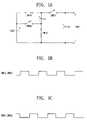
- FIG. 1Ais a circuit diagram showing a general charge pump circuit
- FIGS. 1B and 1Care graphs showing on-off operations of the switches SWC 1 , SWC 2 , SWC 3 and SWC 4 .
- the first capacitor C 1is charged with the charges of the battery.
- the first and second switches SWC 1 and SWC 2are turned-off and the switches SWG 1 and SWG 2 are turned-on, the charges accumulated at the first capacitor C 1 and the charges of the battery are charged at the second capacitor C 2 .
- the second capacitor C 2regulates (or smoothes) an output voltage signal VCP of the charge pump.
- the output voltage signal VCP of the charge pumphas ripples due to variation of an output load since the charge pump does not perform regulating operation according to the variation of the output load.
- Liquid crystal display devicesemploy a capacitor and generate gray scale voltage signals (or data voltage signals), and the liquid crystal display devices employs a capacitor having a large capacitance so as to reduce the ripples.
- the capacitor having the large capacitancemay induce increased size of the charge pump circuit of the liquid crystal display devices.
- ripplesmay not completely be prevented.
- ripple (or water-fall) phenomenonis shown on the display screen of the liquid crystal display device.
- the ripple (or water-fall) phenomenonis serious in the liquid crystal display devices having small/medium display screen that is driven using line inversion method.
- FIG. 2Bis a graph showing a waveform of a voltage signal VCP output from a charge pump employed in a liquid crystal display device
- FIG. 2Ais a graph showing a waveform of a voltage signal VD that is obtained after regulating the voltage signal VD of FIG. 2B .
- the voltage signal VCPis a square wave signal generated from the charge pump.
- a capacitoris coupled to the charge pump so as to regulate the square wave, a reference gray scale voltage signal VD of FIG. 2A is obtained.
- the waveform of the reference gray scale voltage signal VD of FIG. 2Ahas ripples.
- the capacitor coupled to the charge pump so as to regulate the square wavehas a large capacitance.
- the gray scale voltage signals (or data voltage signals) corresponding to ‘a’ point, ‘b’ point or ‘c’ point of the reference gray scale voltage signal VDmay be applied to data lines of a liquid crystal display panel.
- point (‘a’, ‘b’ or ‘c’, etc.) of the reference gray scale voltage signal VDwill be shown as the gray scale voltage signals.
- the ripple phenomenonis serious in middle gray scale levels in which the voltage deviation between gray scale levels is small.
- a middle gray scale levelsuch as 32-gray scale level
- the gray scale voltage level corresponding to ‘a’ point of the reference gray scale voltage signal VDis difference from the gray scale voltage level corresponding to ‘b’ point of the reference gray scale voltage signal VD
- the voltage deviation between gray scale levelsis generated, and ripples are shown on the display screen.
- a gray scale voltage level corresponding to a point between ‘a’ and ‘b’ points of the reference gray scale voltage signal VDmay be applied to a portion of the display screen and a gray scale voltage level corresponding to a point between ‘b’ and ‘c’ points of the reference gray scale voltage signal VD may be applied to another portion of the display screen, thus ripples are shown on the display screen.
- the present inventionis provided to substantially obviate one or more problems due to limitations and disadvantages of the related art.
- a device for driving a display apparatusincludes a timing circuit and a data driver.
- the timing circuitis configured to generate a control signal.
- the data driveris configured to sample a first gray scale voltage signal in response to the control signal, and configured to generate a second gray scale voltage signal to provide a display panel of the display apparatus with the second gray scale voltage signal.
- the second gray scale voltage signalhas a sampled voltage level of the first gray scale voltage signal, and the sampled voltage level is synchronized with the control signal.
- a device for driving a display apparatus having a display panelincludes a scan driver, above mentioned timing circuit and data driver.
- the display panelhas a plurality of scan lines, a plurality of data lines and a plurality of pixels.
- the scan driveris configured to generate a plurality of scan signals activating the scan lines.
- a display apparatusin still another exemplary embodiment, includes a display panel, above mentioned scan driver, timing circuit and data driver.
- the display panelhas a plurality of scan lines, a plurality of data lines and a plurality of pixels.
- a method of driving a display apparatusincludes: generating a control signal; and generating a second gray scale voltage signal by sampling a first gray scale voltage signal in response to the control signal to provide the display apparatus with the second gray scale voltage signal.
- the second gray scale voltage signalhas a sampled voltage level of the first gray scale voltage signal, and the sampled voltage level is synchronized with the control signal.
- FIG. 1Ais a circuit diagram showing a general charge pump circuit
- FIGS. 1B and 1Care graphs showing on-off operations of the switches SWC 1 , SWC 2 , SWC 3 and SWC 4 ;
- FIG. 2Bis a graph showing a waveform of a voltage signal VCP output from a charge pump employed in a liquid crystal display device
- FIG. 2Ais a graph showing a waveform of a voltage signal VD that is obtained after regulating the voltage signal VD of FIG. 2B ;
- FIG. 3is a block diagram showing a liquid crystal display device according to one exemplary embodiment of the present invention.
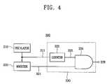
- FIG. 4is a circuit diagram showing a timing circuit of FIG. 3 according to one exemplary embodiment of the present invention.
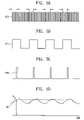
- FIGS. 5A , 5 B, 5 C and 5 Dare graphs showing the waveforms of the signals for describing the operation of the timing circuit of FIG. 4 ;
- FIG. 6is a block diagram showing a data driver of FIG. 3 according to one exemplary embodiment of the present invention.
- FIG. 3is a block diagram showing a liquid crystal display device according to one exemplary embodiment of the present invention.
- the liquid crystal display deviceincludes a liquid crystal display panel 100 , a controller 200 , a timing circuit 300 , a common voltage generator 400 , a data driver 500 and a scan driver 600 .
- the controller 200 , the timing circuit 300 , the common voltage generator 400 , the data driver 500 , and the scan driver 600drive the liquid crystal display panel 100 .
- the liquid crystal display panel 100includes a plurality of pixels.
- a plurality of scan linesis arranged in a row direction, and a plurality of data lines is arranged in a column direction.
- Each of the pixelsincludes a switching element, a liquid crystal capacitor CLC and a storage capacitor CST.
- the switching elementis coupled to a scan line and a data line.
- the switching elementincludes a thin film transistor (TFT).
- TFTthin film transistor
- the liquid crystal capacitor CLCis connected between a drain electrode of the TFT and a common electrode.
- the storage capacitor CSTcharges the liquid crystal capacitor CLC during a vertical synchronization period.
- R (red), G (Green) and B (Blue) dataare supplied from an external graphic controller, and the controller 200 generates image data, for example D 00 ⁇ D 05 , D 10 ⁇ D 15 and D 20 -D 25 , based on the RGB data (DR, DG and DB), respectively, and provides the image data D 00 ⁇ D 05 , D 10 ⁇ D 15 and D 20 -D 25 to the data driver 500 .
- Gray scale voltage signalsare generated based on the image data D 00 ⁇ D 05 , D 10 ⁇ D 15 and D 20 -D 25 by the data driver 500 , and are provided to the source electrode of the TFT via the data lines.
- the scan signalsare generated in response to a horizontal synchronization signal (HSYNC) and a vertical synchronization signal (VSYNC), and are applied to the gate electrode of the TFT while common voltage Vcom is applied to the common electrode of the liquid crystal capacitor CLC.
- HSYNChorizontal synchronization signal
- VSYNCvertical synchronization signal
- the R (red), G (Green) and B (Blue) dataare expressed using 6 bits, respectively, and the image data D 00 ⁇ D 05 , D 10 ⁇ D 15 and D 20 -D 25 are expressed using 18 bits.
- the controller 200generates a clock signal CLK, a polarization signal POL and a vertical start pulse STV based on a dot clock signal DCLK, the horizontal synchronization signal (HSYNC) and the vertical synchronization signal (VSYNC), and provides the clock signal CLK to the data driver 500 , the polarization signal POL to the data driver 500 and the common voltage generator 400 , and the vertical start pulse STV to the scan driver 600 .
- the clock signal CLKmay have the same frequency as the dot clock signal DCLK or different frequency from the dot clock signal DCLK.
- the polarization signal POLis inverted every horizontal synchronization period (or every line) and is used for AC (alternate current) driving of the liquid crystal display panel 100 .
- the vertical start pulse STVhas the same period as the vertical synchronization signal (VSYNC).
- the timing circuit 300generates a control signal STH and provides the data driver 500 with the control signal STH.
- the common voltage generator 400receives the polarization signal POL and generates a common voltage Vcom to provide the common voltage Vcom to the common electrode of the liquid crystal display panel 100 .
- the common voltage Vcomhas a ground potential or a power voltage level VDD.
- the common voltage generator 400provides the common voltage Vcom having the ground potential to the common electrode when the polarization signal POL has a high level, and provides the common voltage Vcom having the power voltage level VDD to the common electrode when the polarization signal POL has a low level
- the data driver 500selects one of the gray scale voltage signals using the clock signal CLK, the image data D 00 ⁇ D 05 , D 10 ⁇ D 15 and D 20 -D 25 and the control signal STH, and outputs the selected gray scale voltage signals to the data lines of the liquid crystal display panel 100 .
- the data driver 500includes a resistor array (not shown) having cascade-connected resistors.
- the resistor arrayfunctions as a voltage divider that divides the reference gray scale voltage signals into a plurality of gray scale voltage signals.
- the scan driver 600generates a plurality of scan signals for activating the scan lines in response to the vertical start pulse STV, and provides the scan lines of the liquid crystal display panel 100 with the scan signals sequentially.
- FIG. 4is a circuit diagram showing a timing circuit of FIG. 3 according to one exemplary embodiment of the present invention
- FIGS. 5A , 5 B, 5 C and 5 Dare graphs showing the waveforms of the signals for describing the operation of the timing circuit of FIG. 4 .
- the timing circuit 300includes an oscillator 310 , a booster 320 and an operation circuit 330 .
- the oscillator 310generates a first oscillating signal 311 and provides the booster 320 and the operation circuit 330 with the first oscillating signal 311 .
- the booster 320boosts the first oscillating signal 311 to generate a second oscillating signal 321 , and provides the operation circuit 330 with the second oscillating signal 321 .
- the liquid crystal display devices applied to mobile phone having small/medium display screenincludes a charge pump since the power consumption is small and small driver IC is used therein.
- An example of the charge pumpis shown in FIGS. 1A , 1 B and 1 C.
- the operation circuit 330includes a counter 332 and an AND gate 334 .
- the operation circuit 330generates the control signal STH based on the first and second oscillating signals 311 and 321 , and provides the control signal STH to the data driver 500 .
- the counter 332receives the first oscillating signal 311 , counts the number of pulses of the first oscillating signal 311 of FIG. 5 , generates a square wave signal 333 when the number of the pulses satisfies a given condition, and provides the square wave signal 333 to the AND gate 334 .
- the square wave signal 333may be activated in response to every given number of the pulses of the first oscillating signal 311 .
- the counter 332outputs the square wave signal 333 every four pulses of the first oscillating signal 311 after the second oscillating signal 321 is activated.
- the AND gate 334performs a logical AND operation on the second oscillating signal 321 and the square wave signal 333 to generate the control signal.STH when the AND gate 334 receives the second oscillating signal 321 having an active level and the square wave signal 333 having an active level.
- the data driver 500outputs the gray scale voltage signal corresponding to a given point, for example ‘a’ point, of the reference gray scale voltage signal in response to the control signal STH. Since the gray scale voltage signals are applied to the data lines in a predetermined timing, the ripples are not generated, and the deterioration of the display quality may be prevented.
- the size of the liquid crystal display device using the charge pump circuitmay be reduced because the capacitor coupled to the output terminal of the charge pump circuit has a low capacitance and the capacitor having a high capacitance may not be required at the output terminal of the charge pump so as to reduce the ripples, and thus the manufacturing cost may be reduced.
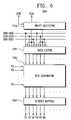
- FIG. 6is a block diagram showing a data driver of FIG. 3 according to one exemplary embodiment of the present invention.
- the data driver 500includes a shift register 510 , a data latch 520 , a digital-to-analog converter (DAC) 530 and an output buffer 540 .
- the data driver 500outputs the gray scale voltage signals (or data voltage signals) to the data lines of the liquid crystal display panel 100 in response to the control signal STH supplied from the timing circuit 300 .
- the shift register 510receives the clock signal CLK and the control signal STH, and outputs the clock signal CLK in response to an active period of the control signal STH to provide the shifted clock signals CLK to the data latch 520 .
- the data latch 520receives the shifted clock signals CLK and the image data, for example D 00 ⁇ D 05 , D 10 ⁇ D 15 and D 20 -D 25 , and latches the value of the image data D 00 ⁇ D 05 , D 10 ⁇ D 15 and D 20 -D 25 at an instance when the clock signal CLK synchronized with the active period of the control signal STH is input to the data latch 520 .
- the data latch 520includes a plurality of latch circuits, and each of the latch circuits receives the clock signal CLK and one of the image data D 00 ⁇ D 05 , D 10 ⁇ D 15 and D 20 -D 25 .
- the latch circuit turned on by the clock signal CLKlatches one of the image data D 00 ⁇ D 05 , D 10 ⁇ D 15 and D 20 -D 25 .
- the data latch 520temporarily stores the image data D 00 ⁇ D 05 , D 10 ⁇ D 15 and D 20 -D 25 .
- the data latch 520outputs the stored image data D 00 ⁇ D 05 , D 10 ⁇ D 15 and D 20 -D 25 to the DAC 530 in response to the shifted clock signal CLK.
- the DAC 530receives a plurality of reference gray scale voltage signals to provide the output buffer 540 with analog gray scale voltage signals corresponding to the values of the image data D 00 ⁇ D 05 , D 10 ⁇ D 15 and D 20 -D 25 supplied from the data latch 520 .
- the DAC 530receives nine reference gray scale voltage signals (V 1 , V 2 , . . . , V 9 ), divides the nine reference gray scale voltage signals (V 1 , V 2 , . . .
- V 9into 256 gray scale voltage signals, generates the analog gray scale voltage signals corresponding to the values of the image data D 00 ⁇ D 05 , D 10 ⁇ D 15 and D 20 -D 25 based on the 256 gray scale voltage signals, and outputs the analog gray scale voltage signals to the output buffer 540 .
- the output buffer 540buffers the analog gray scale voltage signals to output the buffered analog gray scale voltage signals to the data lines of the liquid crystal display panel 100 line by line.
- driver circuit for driving the liquid crystal display devicethe driver circuit for driving organic electroluminescence devices could be utilized.
Landscapes
- Engineering & Computer Science (AREA)
- Physics & Mathematics (AREA)
- Computer Hardware Design (AREA)
- General Physics & Mathematics (AREA)
- Theoretical Computer Science (AREA)
- Chemical & Material Sciences (AREA)
- Crystallography & Structural Chemistry (AREA)
- Control Of Indicators Other Than Cathode Ray Tubes (AREA)
- Liquid Crystal Display Device Control (AREA)
- Liquid Crystal (AREA)
Abstract
Description
Claims (11)
Applications Claiming Priority (2)
| Application Number | Priority Date | Filing Date | Title |
|---|---|---|---|
| KR1020030062615AKR100959780B1 (en) | 2003-09-08 | 2003-09-08 | Liquid crystal display, drive device and method thereof |
| KR2003-62615 | 2003-09-08 |
Publications (2)
| Publication Number | Publication Date |
|---|---|
| US20050052401A1 US20050052401A1 (en) | 2005-03-10 |
| US7548227B2true US7548227B2 (en) | 2009-06-16 |
Family
ID=34225456
Family Applications (1)
| Application Number | Title | Priority Date | Filing Date |
|---|---|---|---|
| US10/922,595Expired - Fee RelatedUS7548227B2 (en) | 2003-09-08 | 2004-08-20 | Display apparatus, device for driving the display apparatus, and method of driving the display apparatus |
Country Status (5)
| Country | Link |
|---|---|
| US (1) | US7548227B2 (en) |
| JP (1) | JP2005084687A (en) |
| KR (1) | KR100959780B1 (en) |
| CN (1) | CN100587783C (en) |
| TW (1) | TW200513731A (en) |
Families Citing this family (10)
| Publication number | Priority date | Publication date | Assignee | Title |
|---|---|---|---|---|
| GB0411314D0 (en)* | 2004-05-21 | 2004-06-23 | Koninkl Philips Electronics Nv | Electronic device with multiple array devices |
| US7746330B2 (en)* | 2005-12-22 | 2010-06-29 | Au Optronics Corporation | Circuit and method for improving image quality of a liquid crystal display |
| KR101311300B1 (en) | 2006-12-29 | 2013-09-25 | 엘지디스플레이 주식회사 | Liquid crystal display device |
| KR20090105148A (en)* | 2008-04-01 | 2009-10-07 | 삼성전자주식회사 | Display device |
| KR20100078699A (en)* | 2008-12-30 | 2010-07-08 | 삼성전자주식회사 | Apparatus and method for power control of amoled |
| KR101579272B1 (en)* | 2009-10-30 | 2015-12-22 | 삼성디스플레이 주식회사 | Display device |
| KR101146983B1 (en)* | 2010-02-12 | 2012-05-23 | 삼성모바일디스플레이주식회사 | A displaying apparatus, and an apparatus and a method for driving the displaying apparatus |
| KR102131307B1 (en) | 2013-12-12 | 2020-07-08 | 삼성디스플레이 주식회사 | Display deivce |
| KR102439795B1 (en) | 2015-07-31 | 2022-09-06 | 삼성디스플레이 주식회사 | Data driver and display device including same |
| CN114170965B (en)* | 2021-11-25 | 2023-03-17 | Tcl华星光电技术有限公司 | Display driving method and display |
Citations (13)
| Publication number | Priority date | Publication date | Assignee | Title |
|---|---|---|---|---|
| EP0899712A2 (en) | 1997-08-29 | 1999-03-03 | Sony Corporation | Column driver for an active matrix liquid crystal display |
| US6122185A (en)* | 1997-07-22 | 2000-09-19 | Seiko Instruments R&D Center Inc. | Electronic apparatus |
| CN1291762A (en) | 1999-08-05 | 2001-04-18 | 恩泰克研究株式会社 | Source driver circuit of liquid crystal display and method thereof |
| US20020060673A1 (en)* | 2000-09-29 | 2002-05-23 | Sanyo Electric Co., Ltd. | Driving device for display device |
| US6411162B2 (en)* | 2000-03-23 | 2002-06-25 | Kabushiki Kaisha Toshiba | Amplifier device and LCD device |
| US20020089485A1 (en)* | 2000-11-22 | 2002-07-11 | Won-Bong Youn | Liquid crystal display with multi-frame inverting function and an apparatus and a method for driving the same |
| US20020093475A1 (en)* | 2001-01-16 | 2002-07-18 | Nec Corporation | Method and circuit for driving liquid crystal display, and portable electronic device |
| US20020167502A1 (en)* | 1999-01-08 | 2002-11-14 | Semiconductor Energy Laboratory Co., Ltd. | Semiconductor display device and driving circuit therefor |
| US20030034947A1 (en) | 1998-03-25 | 2003-02-20 | Sharp Kabushiki Kaisha | Method of driving liquid crystal panel, and liquid crystal display apparatus |
| US6542150B1 (en)* | 1996-06-28 | 2003-04-01 | Cirrus Logic, Inc. | Method and apparatus for asynchronous display of graphic images |
| US20030132903A1 (en)* | 2002-01-16 | 2003-07-17 | Shiro Ueda | Liquid crystal display device having an improved precharge circuit and method of driving same |
| US20030184511A1 (en)* | 2002-03-29 | 2003-10-02 | Fujitsu Display Technologies Corporation | Liquid crystal display and driver thereof |
| US20040070589A1 (en)* | 2002-08-27 | 2004-04-15 | Seiko Epson Corporation | Display driver circuit and display device |
Family Cites Families (7)
| Publication number | Priority date | Publication date | Assignee | Title |
|---|---|---|---|---|
| JP3494611B2 (en)* | 2000-03-23 | 2004-02-09 | シャープ株式会社 | Display device and power supply circuit thereof |
| JP2001286126A (en)* | 2000-03-31 | 2001-10-12 | Sanyo Electric Co Ltd | Charge pump power source circuit, display drive device using it and display |
| JP2002207447A (en)* | 2001-01-11 | 2002-07-26 | Seiko Epson Corp | Power supply circuit, drive circuit, electro-optical device and electronic equipment |
| JP3430155B2 (en)* | 2001-01-31 | 2003-07-28 | Necエレクトロニクス株式会社 | Power boost circuit |
| KR100740933B1 (en)* | 2001-04-13 | 2007-07-19 | 삼성전자주식회사 | Liquid crystal display |
| JP2003005715A (en) | 2001-06-18 | 2003-01-08 | Matsushita Electric Ind Co Ltd | Display device, power supply method thereof, and image display application device |
| US6919838B2 (en)* | 2001-11-09 | 2005-07-19 | Pulse-Link, Inc. | Ultra-wideband imaging system |
- 2003
- 2003-09-08KRKR1020030062615Apatent/KR100959780B1/ennot_activeExpired - Fee Related
- 2004
- 2004-08-20USUS10/922,595patent/US7548227B2/ennot_activeExpired - Fee Related
- 2004-08-26TWTW093125532Apatent/TW200513731A/enunknown
- 2004-09-03JPJP2004256728Apatent/JP2005084687A/enactivePending
- 2004-09-08CNCN200410076867Apatent/CN100587783C/ennot_activeExpired - Fee Related
Patent Citations (13)
| Publication number | Priority date | Publication date | Assignee | Title |
|---|---|---|---|---|
| US6542150B1 (en)* | 1996-06-28 | 2003-04-01 | Cirrus Logic, Inc. | Method and apparatus for asynchronous display of graphic images |
| US6122185A (en)* | 1997-07-22 | 2000-09-19 | Seiko Instruments R&D Center Inc. | Electronic apparatus |
| EP0899712A2 (en) | 1997-08-29 | 1999-03-03 | Sony Corporation | Column driver for an active matrix liquid crystal display |
| US20030034947A1 (en) | 1998-03-25 | 2003-02-20 | Sharp Kabushiki Kaisha | Method of driving liquid crystal panel, and liquid crystal display apparatus |
| US20020167502A1 (en)* | 1999-01-08 | 2002-11-14 | Semiconductor Energy Laboratory Co., Ltd. | Semiconductor display device and driving circuit therefor |
| CN1291762A (en) | 1999-08-05 | 2001-04-18 | 恩泰克研究株式会社 | Source driver circuit of liquid crystal display and method thereof |
| US6411162B2 (en)* | 2000-03-23 | 2002-06-25 | Kabushiki Kaisha Toshiba | Amplifier device and LCD device |
| US20020060673A1 (en)* | 2000-09-29 | 2002-05-23 | Sanyo Electric Co., Ltd. | Driving device for display device |
| US20020089485A1 (en)* | 2000-11-22 | 2002-07-11 | Won-Bong Youn | Liquid crystal display with multi-frame inverting function and an apparatus and a method for driving the same |
| US20020093475A1 (en)* | 2001-01-16 | 2002-07-18 | Nec Corporation | Method and circuit for driving liquid crystal display, and portable electronic device |
| US20030132903A1 (en)* | 2002-01-16 | 2003-07-17 | Shiro Ueda | Liquid crystal display device having an improved precharge circuit and method of driving same |
| US20030184511A1 (en)* | 2002-03-29 | 2003-10-02 | Fujitsu Display Technologies Corporation | Liquid crystal display and driver thereof |
| US20040070589A1 (en)* | 2002-08-27 | 2004-04-15 | Seiko Epson Corporation | Display driver circuit and display device |
Non-Patent Citations (1)
| Title |
|---|
| Chinese Office Action for application No. 200410076867.1, dated Sep. 28, 2007, and an English translation thereof, citing the above cited references. |
Also Published As
| Publication number | Publication date |
|---|---|
| US20050052401A1 (en) | 2005-03-10 |
| CN1595489A (en) | 2005-03-16 |
| KR100959780B1 (en) | 2010-05-27 |
| CN100587783C (en) | 2010-02-03 |
| TW200513731A (en) | 2005-04-16 |
| JP2005084687A (en) | 2005-03-31 |
| KR20050025779A (en) | 2005-03-14 |
Similar Documents
| Publication | Publication Date | Title |
|---|---|---|
| KR101326075B1 (en) | Liquid crystal display divice and driving method thereof | |
| US8305321B2 (en) | Apparatus for driving source lines and display apparatus having the same | |
| US7643000B2 (en) | Output buffer and power switch for a liquid crystal display and method of driving thereof | |
| US20070085801A1 (en) | Flat panel display and method of driving the same | |
| US6566643B2 (en) | Electro-optical device, method of driving the same, and electronic apparatus using the same | |
| KR20080011896A (en) | Gate-on voltage generator circuit and gate-off voltage generator circuit and liquid crystal display device having them | |
| US7330066B2 (en) | Reference voltage generation circuit that generates gamma voltages for liquid crystal displays | |
| KR100995625B1 (en) | LCD and its driving method | |
| US9117512B2 (en) | Gate shift register and flat panel display using the same | |
| KR100637060B1 (en) | Analog buffer and driving method thereof, liquid crystal display using same and driving method thereof | |
| US20050046647A1 (en) | Method of driving data lines, apparatus for driving data lines and display device having the same | |
| US7548227B2 (en) | Display apparatus, device for driving the display apparatus, and method of driving the display apparatus | |
| US9087493B2 (en) | Liquid crystal display device and driving method thereof | |
| KR20040009817A (en) | A liquid crystal display apparatus | |
| KR101284940B1 (en) | Apparatus and method for driving a liquid crystal display | |
| KR101529554B1 (en) | Liquid crystal display device | |
| KR100806247B1 (en) | Method of driving lcd panels | |
| KR101232174B1 (en) | Eliminating afterimage circuit for liquid crystal display device and method for driving the same | |
| JPH0362094A (en) | Gradation display driving circuit of active matrix type liquid crystal display device | |
| KR100274547B1 (en) | A tft transistor gate drive voltage output circuit and a lcd device having the circuit | |
| KR20110035421A (en) | Driving device of liquid crystal display and driving method thereof | |
| JP2011085801A (en) | Tft liquid crystal drive circuit, and tft liquid crystal drive method using the same | |
| KR101752779B1 (en) | ORGANIC LIGHT EMITTING DIODE DISPLAY DEVICE AND Method Of DRIVING THE SAME | |
| KR100443830B1 (en) | Liquid Crystal Display and Driving Method Thereof | |
| KR101097585B1 (en) | Voltage Generating Circuit For Liquid Crystal Display And Liquid Crystal Display Using The Same |
Legal Events
| Date | Code | Title | Description |
|---|---|---|---|
| AS | Assignment | Owner name:SAMSUNG ELECTRONICS CO., LTD., KOREA, REPUBLIC OF Free format text:ASSIGNMENT OF ASSIGNORS INTEREST;ASSIGNOR:LEE, SUNG-HO;REEL/FRAME:015717/0548 Effective date:20040806 | |
| FEPP | Fee payment procedure | Free format text:PAYOR NUMBER ASSIGNED (ORIGINAL EVENT CODE: ASPN); ENTITY STATUS OF PATENT OWNER: LARGE ENTITY | |
| STCF | Information on status: patent grant | Free format text:PATENTED CASE | |
| FEPP | Fee payment procedure | Free format text:PAYOR NUMBER ASSIGNED (ORIGINAL EVENT CODE: ASPN); ENTITY STATUS OF PATENT OWNER: LARGE ENTITY Free format text:PAYER NUMBER DE-ASSIGNED (ORIGINAL EVENT CODE: RMPN); ENTITY STATUS OF PATENT OWNER: LARGE ENTITY | |
| AS | Assignment | Owner name:SAMSUNG DISPLAY CO., LTD., KOREA, REPUBLIC OF Free format text:ASSIGNMENT OF ASSIGNORS INTEREST;ASSIGNOR:SAMSUNG ELECTRONICS CO., LTD.;REEL/FRAME:028984/0774 Effective date:20120904 | |
| FPAY | Fee payment | Year of fee payment:4 | |
| FPAY | Fee payment | Year of fee payment:8 | |
| FEPP | Fee payment procedure | Free format text:MAINTENANCE FEE REMINDER MAILED (ORIGINAL EVENT CODE: REM.); ENTITY STATUS OF PATENT OWNER: LARGE ENTITY | |
| LAPS | Lapse for failure to pay maintenance fees | Free format text:PATENT EXPIRED FOR FAILURE TO PAY MAINTENANCE FEES (ORIGINAL EVENT CODE: EXP.); ENTITY STATUS OF PATENT OWNER: LARGE ENTITY | |
| STCH | Information on status: patent discontinuation | Free format text:PATENT EXPIRED DUE TO NONPAYMENT OF MAINTENANCE FEES UNDER 37 CFR 1.362 | |
| FP | Lapsed due to failure to pay maintenance fee | Effective date:20210616 |