US7547633B2 - UV assisted thermal processing - Google Patents
UV assisted thermal processingDownload PDFInfo
- Publication number
- US7547633B2 US7547633B2US11/414,869US41486906AUS7547633B2US 7547633 B2US7547633 B2US 7547633B2US 41486906 AUS41486906 AUS 41486906AUS 7547633 B2US7547633 B2US 7547633B2
- Authority
- US
- United States
- Prior art keywords
- chamber
- substrate
- energy
- assembly
- radiation
- Prior art date
- Legal status (The legal status is an assumption and is not a legal conclusion. Google has not performed a legal analysis and makes no representation as to the accuracy of the status listed.)
- Expired - Fee Related, expires
Links
- 238000012545processingMethods0.000titleclaimsabstractdescription53
- 230000005855radiationEffects0.000claimsabstractdescription72
- 239000000758substrateSubstances0.000claimsabstractdescription61
- 238000000034methodMethods0.000claimsabstractdescription27
- VYPSYNLAJGMNEJ-UHFFFAOYSA-Nsilicon dioxideInorganic materialsO=[Si]=OVYPSYNLAJGMNEJ-UHFFFAOYSA-N0.000claimsdescription29
- 239000010453quartzSubstances0.000claimsdescription27
- 238000010438heat treatmentMethods0.000claimsdescription7
- 239000002243precursorSubstances0.000claimsdescription6
- 239000004065semiconductorSubstances0.000abstractdescription4
- 235000012239silicon dioxideNutrition0.000description25
- 239000007789gasSubstances0.000description11
- 230000003647oxidationEffects0.000description9
- 238000007254oxidation reactionMethods0.000description9
- 238000001816coolingMethods0.000description8
- QVGXLLKOCUKJST-UHFFFAOYSA-Natomic oxygenChemical compound[O]QVGXLLKOCUKJST-UHFFFAOYSA-N0.000description7
- 239000001301oxygenSubstances0.000description7
- 229910052760oxygenInorganic materials0.000description7
- GQPLMRYTRLFLPF-UHFFFAOYSA-NNitrous OxideChemical compound[O-][N+]#NGQPLMRYTRLFLPF-UHFFFAOYSA-N0.000description6
- 238000006243chemical reactionMethods0.000description6
- 239000000463materialSubstances0.000description5
- 210000002381plasmaAnatomy0.000description5
- 238000009792diffusion processMethods0.000description4
- 229910052736halogenInorganic materials0.000description4
- QGZKDVFQNNGYKY-UHFFFAOYSA-NAmmoniaChemical compoundNQGZKDVFQNNGYKY-UHFFFAOYSA-N0.000description3
- IJGRMHOSHXDMSA-UHFFFAOYSA-NAtomic nitrogenChemical compoundN#NIJGRMHOSHXDMSA-UHFFFAOYSA-N0.000description3
- CURLTUGMZLYLDI-UHFFFAOYSA-NCarbon dioxideChemical compoundO=C=OCURLTUGMZLYLDI-UHFFFAOYSA-N0.000description3
- 229910052782aluminiumInorganic materials0.000description3
- XAGFODPZIPBFFR-UHFFFAOYSA-NaluminiumChemical compound[Al]XAGFODPZIPBFFR-UHFFFAOYSA-N0.000description3
- 238000000137annealingMethods0.000description3
- 229910052751metalInorganic materials0.000description3
- 239000002184metalSubstances0.000description3
- 239000001272nitrous oxideSubstances0.000description3
- 229910001369BrassInorganic materials0.000description2
- UGFAIRIUMAVXCW-UHFFFAOYSA-NCarbon monoxideChemical compound[O+]#[C-]UGFAIRIUMAVXCW-UHFFFAOYSA-N0.000description2
- MWUXSHHQAYIFBG-UHFFFAOYSA-NNitric oxideChemical compoundO=[N]MWUXSHHQAYIFBG-UHFFFAOYSA-N0.000description2
- 239000010951brassSubstances0.000description2
- 229910002092carbon dioxideInorganic materials0.000description2
- 239000001569carbon dioxideSubstances0.000description2
- 229910002091carbon monoxideInorganic materials0.000description2
- 238000011109contaminationMethods0.000description2
- 239000002826coolantSubstances0.000description2
- 238000013461designMethods0.000description2
- 230000005284excitationEffects0.000description2
- 239000002245particleSubstances0.000description2
- 230000002093peripheral effectEffects0.000description2
- 230000000979retarding effectEffects0.000description2
- 229910001220stainless steelInorganic materials0.000description2
- 239000010935stainless steelSubstances0.000description2
- VZGDMQKNWNREIO-UHFFFAOYSA-NtetrachloromethaneChemical compoundClC(Cl)(Cl)ClVZGDMQKNWNREIO-UHFFFAOYSA-N0.000description2
- PXGOKWXKJXAPGV-UHFFFAOYSA-NFluorineChemical compoundFFPXGOKWXKJXAPGV-UHFFFAOYSA-N0.000description1
- CBENFWSGALASAD-UHFFFAOYSA-NOzoneChemical compound[O-][O+]=OCBENFWSGALASAD-UHFFFAOYSA-N0.000description1
- 238000010521absorption reactionMethods0.000description1
- 230000004913activationEffects0.000description1
- 150000001412aminesChemical class0.000description1
- 229910021529ammoniaInorganic materials0.000description1
- 230000000712assemblyEffects0.000description1
- 238000000429assemblyMethods0.000description1
- 239000013078crystalSubstances0.000description1
- 230000003247decreasing effectEffects0.000description1
- 229910001873dinitrogenInorganic materials0.000description1
- 238000005516engineering processMethods0.000description1
- 239000011737fluorineSubstances0.000description1
- 229910052731fluorineInorganic materials0.000description1
- VHHHONWQHHHLTI-UHFFFAOYSA-NhexachloroethaneChemical compoundClC(Cl)(Cl)C(Cl)(Cl)ClVHHHONWQHHHLTI-UHFFFAOYSA-N0.000description1
- WMIYKQLTONQJES-UHFFFAOYSA-NhexafluoroethaneChemical compoundFC(F)(F)C(F)(F)FWMIYKQLTONQJES-UHFFFAOYSA-N0.000description1
- 150000002429hydrazinesChemical class0.000description1
- QSHDDOUJBYECFT-UHFFFAOYSA-NmercuryChemical compound[Hg]QSHDDOUJBYECFT-UHFFFAOYSA-N0.000description1
- 229910052753mercuryInorganic materials0.000description1
- 229910052757nitrogenInorganic materials0.000description1
- 229910000069nitrogen hydrideInorganic materials0.000description1
- 230000003287optical effectEffects0.000description1
- 238000005457optimizationMethods0.000description1
- 238000013021overheatingMethods0.000description1
- 239000007800oxidant agentSubstances0.000description1
- 230000001590oxidative effectEffects0.000description1
- 238000005215recombinationMethods0.000description1
- 230000006798recombinationEffects0.000description1
- 238000007789sealingMethods0.000description1
- 239000000377silicon dioxideSubstances0.000description1
- 229910052709silverInorganic materials0.000description1
- 239000004332silverSubstances0.000description1
- SFZCNBIFKDRMGX-UHFFFAOYSA-Nsulfur hexafluorideChemical compoundFS(F)(F)(F)(F)FSFZCNBIFKDRMGX-UHFFFAOYSA-N0.000description1
- TXEYQDLBPFQVAA-UHFFFAOYSA-NtetrafluoromethaneChemical compoundFC(F)(F)FTXEYQDLBPFQVAA-UHFFFAOYSA-N0.000description1
- 238000012546transferMethods0.000description1
- XLYOFNOQVPJJNP-UHFFFAOYSA-NwaterSubstancesOXLYOFNOQVPJJNP-UHFFFAOYSA-N0.000description1
- 229910052724xenonInorganic materials0.000description1
- FHNFHKCVQCLJFQ-UHFFFAOYSA-Nxenon atomChemical compound[Xe]FHNFHKCVQCLJFQ-UHFFFAOYSA-N0.000description1
Images


Classifications
- H—ELECTRICITY
- H01—ELECTRIC ELEMENTS
- H01L—SEMICONDUCTOR DEVICES NOT COVERED BY CLASS H10
- H01L21/00—Processes or apparatus adapted for the manufacture or treatment of semiconductor or solid state devices or of parts thereof
- H01L21/67—Apparatus specially adapted for handling semiconductor or electric solid state devices during manufacture or treatment thereof; Apparatus specially adapted for handling wafers during manufacture or treatment of semiconductor or electric solid state devices or components ; Apparatus not specifically provided for elsewhere
- H01L21/67005—Apparatus not specifically provided for elsewhere
- H01L21/67011—Apparatus for manufacture or treatment
- H01L21/67098—Apparatus for thermal treatment
- H01L21/67115—Apparatus for thermal treatment mainly by radiation
- H—ELECTRICITY
- H01—ELECTRIC ELEMENTS
- H01L—SEMICONDUCTOR DEVICES NOT COVERED BY CLASS H10
- H01L21/00—Processes or apparatus adapted for the manufacture or treatment of semiconductor or solid state devices or of parts thereof
- H01L21/02—Manufacture or treatment of semiconductor devices or of parts thereof
- H01L21/04—Manufacture or treatment of semiconductor devices or of parts thereof the devices having potential barriers, e.g. a PN junction, depletion layer or carrier concentration layer
- H01L21/18—Manufacture or treatment of semiconductor devices or of parts thereof the devices having potential barriers, e.g. a PN junction, depletion layer or carrier concentration layer the devices having semiconductor bodies comprising elements of Group IV of the Periodic Table or AIIIBV compounds with or without impurities, e.g. doping materials
- H01L21/30—Treatment of semiconductor bodies using processes or apparatus not provided for in groups H01L21/20 - H01L21/26
- H01L21/324—Thermal treatment for modifying the properties of semiconductor bodies, e.g. annealing, sintering
Definitions
- the present inventionrelates generally to a semiconductor processing tool and, more specifically, to a thermal processing tool with a UV radiation source.
- Rapid Thermal Processingcommonly referred to as ‘RTP’, subjects a substrate to a very brief, intense burst of heat that can go from room temperature to about 1000° C. in seconds.
- RTP technologyis used to change the characteristics of a deposited film or crystal lattice.
- RTPgenerally includes processes such as annealing, silicidation and oxidation of a substrate surface.
- an RTP chamberincludes a radiant heat source or lamp, a chamber body, and a substrate support ring.
- the lampis typically mounted on a top surface of the chamber body so that the energy generated by the lamp radiates upon the substrate supported by the substrate support ring with in the chamber body.
- a quartz windowis typically disposed in the top surface of the chamber body to facilitate the transfer of energy from the lamp to the substrate.
- An external motoris usually used to rotate the support ring and the substrate to compensate for variations in the radiation energy generated by the lamp that could heat the substrate non-uniformly. Typically, a rapid thermal process is performed at a reduced pressure to get better uniformity.
- Thermal oxidationis commonly used to grow very thin layer of oxide used as gate oxide.
- An oxidation process performed in a state of the art RTP chamberusually include raising the temperature in the RTP chamber high enough to break oxygen or other species used to form an oxide layer and to allow enough diffusion of oxygen or other species occur on the substrate surface.
- the temperature needed to break oxygen or other speciesis usually higher than the temperature needed to induce enough diffusion.
- the higher temperature required for breaking oxygen or other speciesincreases thermal exposure, promote unwanted diffusion inside other structures.
- the present inventionprovides methods and apparatus for performing rapid thermal processing of a semiconductor substrate.
- One embodiment of the present inventionprovides an apparatus for thermal processing a substrate.
- the apparatuscomprises a chamber and a UV radiation assembly disposed inside the chamber.
- the apparatusfurther comprising an outside radiation assembly configured to radiate energy into the chamber through a quartz window on the chamber.
- the apparatuscomprises a chamber having a top window, a substrate support mounted inside the chamber, wherein the substrate support is configured to support the substrate with a processing surface facing the top window, a first energy assembly disposed outside the chamber, wherein the first energy assembly is configured to radiate energy through the top window, and a second energy assembly mounted inside the chamber above the substrate support.
- Yet another embodiment of the present inventionprovides a method for thermal processing a substrate.
- the methodcomprises positioning the substrate in a chamber, applying a first energy source to supply heat to the chamber, and applying a second energy source to generate active species in the chamber.
- FIG. 1illustrates a sectional perspective view of a thermal processing chamber in accordance with one embodiment of the present invention.
- FIG. 2illustrates a perspective view of a UV (ultra violet) assembly in accordance with one embodiment of the present invention.
- FIG. 3illustrates a sectional view of a thermal processing chamber in accordance with one embodiment of the present invention.
- FIG. 4illustrates a sectional view of the thermal processing chamber of FIG. 3 .
- FIG. 5illustrates a perspective view of a UV assembly in accordance with one embodiment of the present invention.
- FIG. 6illustrates a sectional view of an exemplary reflector used in the UV assembly of FIG. 5 .
- FIG. 7illustrates a sectional view of a thermal processing chamber having a UV assembly of FIG. 5 .
- Thermal processing chambers of the present inventioncomprise two different radiation energy sources, such as an infrared radiation source and a UV radiation source.
- the UV radiation source and the infrared radiation sourcemay be used alone or in combination to supply heat, activate electronic, or create active species inside the thermal processing chamber.
- a plurality of processes, such as rapid thermal processing, annealing, and oxidation,may be performed in the thermal processing chamber with improved results.
- the combined use of infrared and UV radiationenables surface selective reactions which is not possible by using either radiation alone.
- FIG. 1illustrates a sectional perspective view of a thermal processing chamber 100 in accordance with one embodiment of the present invention.
- the thermal processing chamber 100generally comprises a lamp assembly 110 , and a chamber 130 having a UV assembly 120 disposed therein.
- the chamber 130is a vacuum chamber. In another embodiment, the chamber 130 may be an atmospheric chamber.
- the lamp assembly 110is positioned above the chamber 130 and configured to supply heat to the chamber 130 via a quartz window 114 of the chamber 130 .
- the lamp assembly 110is configured to house a heating source, such as a plurality of tungsten-halogen lamps configured to provide a tailored infrared heating means to a substrate 101 disposed in the chamber 130 .
- the UV assembly 120is configured to provide a UV source to the chamber 130 , for example to generate active species for reaction on the surface of the substrate 101 in the chamber 130 .
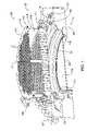
- the lamp assembly 110generally comprises a radiant energy pipe assembly 112 having a plurality of light pipes 111 .
- the light pipes 111may be made of stainless steel, brass, aluminum or other metal.
- Each of the light pipes 111is configured to house a radiant energy source, for example a tungsten-halogen lamp.
- the ends of the light pipes 111are brazed or welded to openings in an upper cooling wall 116 and a lower cooling wall 117 .
- a cylindrical wall 118is brazed or welded to the peripheral edge of the upper cooling wall 116 and the lower cooling wall 117 .
- the light pipes 111may be disposed in a hexagonal arrangement. Coolant may be circulated to the lamp assembly 110 through an inlet 109 to cool the light pipes 111 and to keep to walls 116 , 117 and 118 cool during process.
- the chamber 130generally comprises a circular sidewall 140 defining a chamber volume 139 with the quartz window 114 and a bottom wall (not shown).
- the sidewall 140may have an inlet 131 and an outlet (not shown) configured to connect the chamber volume 139 with a gas source and a pump.
- a silt valvemay be adapted to an opening 137 on the sidewall 140 for a robot to drop/retrieve the substrate 101 on/from a substrate support 138 positioned in the chamber volume 139 .
- the substrate support 138may be configured to move vertically and to rotate about a central axis.
- the UV assembly 120is generally disposed on an upper portion of the chamber volume 139 .
- the UV assembly 120may take form of a module which may be “plugged in” to the chamber 130 .
- Different designs of UV assembliesmay be exchangeably plugged into the chamber 130 to suit different design recipes.
- FIG. 2illustrates a perspective view of the UV assembly 120 used in the thermal processing chamber 100 of FIG. 1 .
- the UV assembly 120generally comprises a top 124 , a bottom 125 and sidewalls 121 , which defines a UV volume 129 therein.
- An opening 126 b on the bottom 125is configured to connect the UV volume 129 with the chamber volume 139 of the chamber 130 shown in FIG. 1 .
- An opening 126 a on the top 124exposes the UV volume 129 to the quartz window 114 of FIG. 114 , hence providing a passage for the radiation energy from the lamp assembly 110 to the chamber volume 139 during process.
- the UV assembly 120further comprises a plurality of quartz tubes 123 with both ends extending out of opposing sidewalls 121 of the UV assembly 120 .
- a removable cap 127may be used for sealing.
- Each of the quartz tubes 123is configured to house a UV lamp 122 (shown in FIG. 1 ) therein.
- the UV lamps 122may include sealed plasma bulbs filled with one or more gases such as xenon (Xe) or mercury (Hg) for excitation by a power source.
- the power sourcemay be a conventional UV power source or one or more transformers to include energize filaments of the magnetrons.
- the power sourcecan introduce radio frequency (RF) energy sources that are capable of excitation of the gases within the UV lamp bulbs.
- the UV lamp bulbmay have low pressure Hg or other low pressure UV producing discharges to produce radiation of 254 nm and 185 nm.
- the UV lamp 122may be positioned in one of the quartz tubes 123 such that electrodes of UV lamps 122 protrude outside the UV volume 129 , or at least are sheltered by the top 124 from the radiation energy of the lamp assembly 110 to keep the electrodes from overheating and to control the pressure in the UV lamp 122 .
- FIG. 3illustrates a sectional view of a thermal processing chamber 200 in accordance with one embodiment of the present invention.
- FIG. 4illustrates a sectional view of the thermal processing chamber 200 of FIG. 3 along 4 - 4 .
- the thermal processing chamber 200generally comprises a lamp assembly 210 , and a chamber 230 having a UV assembly 220 disposed therein.
- the lamp assembly 210is positioned above the chamber 230 and configured to supply heat to the chamber 230 via a quartz window 214 of the chamber 230 .
- the lamp assembly 210is configured to house a heating source, such as a plurality of tungsten-halogen lamps configured to provide a tailored infrared heating means to a substrate 201 disposed in the chamber 230 .
- the UV unitis configured to provide a UV source to the chamber 230 , for example to generate active species for reaction on the surface of the substrate 201 in the chamber 230 .
- the lamp assembly 210generally comprises a plurality of light pipes 211 .
- the light pipes 211may be made of stainless steel, brass, aluminum or other metal.
- Each of the light pipes 211is configured to house a radiant energy source 208 , for example a tungsten-halogen lamp to provide heat to the chamber volume 239 in form of infrared radiation.
- the ends of the light pipes 211are brazed or welded to openings in an upper cooling wall 216 and a lower cooling wall 217 .
- a cylindrical wall 218is brazed or welded to the peripheral edge of the upper cooling wall 216 and the lower cooling wall 217 .
- the light pipes 211may be disposed in a hexagonal arrangement.
- Coolantmay be circulated to the lamp assembly 210 through an inlet 209 to keep to walls cool during process.
- Each of the radiant energy source 208may be connected to a controller 207 which may control the energy level of each radiant energy source 208 to achieve a uniform or tailored heating profile to the chamber volume 239 .
- the radiant energy sources 208may be grouped in a plurality of radial bands. In another embodiment, the radiant energy sources 208 may be controlled individually.
- the chamber 230generally comprises a circular sidewall 240 defining a chamber volume 239 with the quartz window 214 and a bottom wall (not shown).
- the sidewall 240may have an inlet 231 adapted to a gas source 235 configured to provide one or more gases to the chamber volume 239 .
- An outlet 234generally disposed on an opposite side of the sidewall 240 of the inlet 231 , is adapted to a pump 236 .
- a silt valve(not shown) may be adapted to an opening 237 (shown in FIG. 4 ) on the sidewall 240 for a robot to drop/retrieve the substrate 201 on/from a substrate support 238 positioned in the chamber volume 239 .
- the substrate support 238may be configured to move vertically and to rotate about a central axis.
- the UV assembly 220is generally disposed on an upper portion of the chamber volume 239 .
- the UV assembly 220may take the form of a module which may be “plugged in” to the chamber 230 .
- the UV assembly 220may be similar to the UV assembly of FIG. 2 .
- a plurality of quartz tubes 223may be disposed in a parallel manner with both ends extending out of opposing sidewalls 221 of the UV assembly 220 .
- the UV assembly 220may include about 15 quartz tubes 223 evenly distributed on a horizontal plane.
- a UV lamp 222may be disposed in each of the quartz tubes 223 to provide a desired UV resource.
- each of the plurality of quartz tubes 223protrudes out of the sidewalls 221 .
- the UV lamp 222 inside each quart tube 223is placed such that two electrodes 241 of the UV lamp 222 are outside the chamber volume 239 .
- the electrodes 241are adapted to a power supply 206 configured to provide an energy source to each of the UV lamps 222 independently.
- Caps 227may be used to close the quartz tubes 223 .
- Seals 242may be used near the interface of each quartz tube 223 and the sidewall 221 to seal the chamber volume 239 .
- the UV assembly 220 and the lamp assembly 210may be used alone or in combination to supply heat, activate surface sites, or create active species inside the chamber 230 .
- a plurality of processes, such as rapid thermal processing, annealing, and oxidation,may be performed in the thermal processing chamber 200 .
- the lamp assembly 210may be used to provide heat in form of infrared radiation to the substrate 201 disposed in the chamber volume 239 .
- the lamp assembly 210may be adjusted to rapidly heat the substrate 201 uniformly to a temperature that enables diffusion of oxygen through the silicon dioxide product layer in the substrate 201 .
- the UV assembly 220may be used to provide UV radiation generate active species from precursors supplied to the chamber volume 239 through the inlet 231 . It should be noted that the pressure inside the UV lamps 222 are low enough, the UV lamps 222 would absorb very limited amounted of radiation energy from the lamp assembly 210 even though the UV lamps 222 are positioned in the radiation path of the lamp assembly 210 .
- the quartz tubes 223may absorb some radiation energy from the lamp assembly 210 . In one embodiment, the quartz tubes 223 may have rectangular cross sections to minimize the disturbance to the radiant energy profile from the lamp assembly 210 .
- the UV radiation from the UV assembly 220may be used to irradiate precursor that is capable of generating desired active species for treating a film on the substrate.
- the precursorsmay comprises or consist of nitrogen, oxygen, or fluorine.
- other active species and precursorsmay be used.
- the UV radiation sourcemay be tailored to generate different active species. In one embodiment, tailoring the UV radiation source may be achieved by adjusting the gas pressure inside a UV lamp bulb to emit UV radiation of different wavelength.
- UV radiationmay be used to create highly reactive oxidant species near a reactive surface from oxygen (O 2 ), ozone (O 3 ), nitrous oxide (N 2 O), carbon monoxide (CO), carbon dioxide (CO 2 ), water (H 2 O), or combinations thereof in a thermal processing chamber having an infrared radiation source to heat the reactive surface, such as the thermal processing chamber 200 of FIG. 3 .
- UV radiationmay be used to create highly reactive nitridation species near a reactive surface from ammonia (NH 3 ), nitrogen gas (N 2 ), hydrazines, amines, or combinations thereof in a thermal processing chamber having an infrared radiation source to heat the reactive surface, such as the thermal processing chamber 200 of FIG. 3 .
- UV radiationmay be used to create highly reactive oxidation/nitridation species near a reactive surface from nitrous oxide or nitric oxide in a thermal processing chamber having an infrared radiation source to heat the reactive surface, such as the thermal processing chamber 200 of FIG. 3 .
- UV radiationmay be used to create highly reactive fluorinate species near a reactive surface from NF 3 , F 2 , CF 4 , SF 6 , C 2 F 6 , CCl 4 , C 2 Cl 6 , or combinations thereof in a thermal processing chamber having an infrared radiation source to heat the reactive surface, such as the thermal processing chamber 200 of FIG. 3 .
- the quartz tubes 223may be replaced by tubes made from fluorinate resistive materials.
- infrared and UV radiationenables surface selective reactions which are not possible by using either radiation alone.
- surface selective reactionsmay be achieved by combining UV activation and differential surface heating as a result of engineered emissivity differences.
- thermo processing chamberwith both UV radiation source and infrared radiation source.
- using both UV and infrared radiation on some processes, such as oxidationmay shorten the process time because the temperature raise of the substrate may be decreased by using the UV radiation to generate active species instead of using the infrared radiation to generate active species.
- the independent controls of the UV radiation source and infrared radiation sourceenhance uniformity of process results. More particularly, the infrared radiation source, such as the lamp assembly 210 of FIG. 3 , enables rapid flexible substrate temperature control by tailored infrared radiation distribution, while the UV radiation source, such as the UV assembly 220 of FIG. 3 , enables the independent tailored UV distribution for active species and active site generation.
- the configuration of positioning UV radiation source within the infrared radiation regionenables better optimization of the uniformity of both radiation types on the substrate processing surface and in the gas phase in the chamber.
- this configurationcreates active species in the vicinity of the substrate surface enabling creation of very active species close to the location of use and minimizing the loss by recombination or other undesired reactions.
- this configurationalso has advantages in retarding loss of volatile materials from the substrate surface because this configuration enables creation of active species at higher pressure than state of the art method, such as using plasmas.
- the loss of volatile materials from the substrate surfaceis generally undesirable since it leads to loss of desired surface features, to condensate fouling of optical surfaces, and to particle generations.
- Higher pressuresare often useful in retarding loss of volatile materials from the substrate surface.
- in the state of art methods from creating active species, such as plasmasgenerally require low total gas pressures to permit the escape of the active species outside the ionized region of the plasma while keeping the substrate outside the ionized region.
- High density plasmasoften have contamination issues traceable to material exposure to very high temperature which is often the case for high thermal processing.
- UV radiationto irradiate both the substrate surface and the gas phase may lead to enhanced kinetics from simultaneous creation of activated sites and activated species.
- FIG. 5illustrates a perspective view of a UV assembly 320 in accordance with another embodiment of the present invention.
- the UV assembly 320may be used to provide UV radiation to a thermal processing chamber, such as the thermal processing chamber 100 of FIG. 1 and 200 of FIG. 3 .
- the UV assembly 320generally comprises a plurality of sidewalls 321 joint by a plurality of joints 324 to form a polygon.
- the polygonis a square, as shown in FIG. 5 .
- a UV lamp 322 enclosed in a quartz tube 323is generally disposed inside each of the plurality of sidewalls 321 .
- Each of the UV lamps 322 and the quartz tubes 323extend into two neighboring joints 324 wherein electrodes of the UV lamps 322 may be shielded from any radiation inside the chamber the UV assembly 320 resides. This configuration directs the UV radiation energy more towards the gas phase and less towards the substrate surface.
- Single ended UV lamps, such as XERADEX® lampmay be used in this configuration.
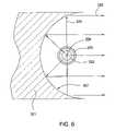
- a plurality of reflectors 327is generally positioned along each of the plurality of sidewalls 321 to reflect UV radiation from the corresponding UV lamp 322 in a desired way.
- the reflectors 327generally have a designed sectional shape to achieve a desirable function.
- the sectional shape of each of the reflectors 327is a parabolic curve.
- the center of the corresponding UV lamp 322is disposed at a focus 328 of the parabolic curve.
- the sectional shape of the reflectors 327may also be elliptical or other types.
- the reflectors 327may have a reflecting surface made from metal, such as aluminum or silver, or from a stack of dielectric films that effectively reflects UV radiation.
- the use of reflectors 327may be used to minimize UV exposure on the surface of the substrate being processed.
- the reflectors 327may also be used as microwave cavities for UV lamps powered by microwave power source.
- FIG. 7illustrates a sectional view of a thermal processing chamber 300 having the UV assembly 320 of FIG. 5 .
- the thermal processing chamber 300is similar to the thermal processing chamber 200 of FIG. 3 except the UV assembly 220 is replaced by the UV assembly 320 .
- the UV lamps 322are outside the radiation region of the lamp assembly 210 . This configuration minimizes the UV radiation on the substrate 201 and the energy absorption of by the quartz tubes 323 during process.
Landscapes
- Engineering & Computer Science (AREA)
- Microelectronics & Electronic Packaging (AREA)
- Condensed Matter Physics & Semiconductors (AREA)
- General Physics & Mathematics (AREA)
- Manufacturing & Machinery (AREA)
- Computer Hardware Design (AREA)
- Physics & Mathematics (AREA)
- Power Engineering (AREA)
- Health & Medical Sciences (AREA)
- Toxicology (AREA)
- Drying Of Semiconductors (AREA)
- Formation Of Insulating Films (AREA)
- Chemical Vapour Deposition (AREA)
Abstract
Description
1. Field of the Invention
The present invention relates generally to a semiconductor processing tool and, more specifically, to a thermal processing tool with a UV radiation source.
2. Description of the Related Art
Rapid Thermal Processing, commonly referred to as ‘RTP’, subjects a substrate to a very brief, intense burst of heat that can go from room temperature to about 1000° C. in seconds. RTP technology is used to change the characteristics of a deposited film or crystal lattice. RTP generally includes processes such as annealing, silicidation and oxidation of a substrate surface.
Generally, an RTP chamber includes a radiant heat source or lamp, a chamber body, and a substrate support ring. The lamp is typically mounted on a top surface of the chamber body so that the energy generated by the lamp radiates upon the substrate supported by the substrate support ring with in the chamber body. A quartz window is typically disposed in the top surface of the chamber body to facilitate the transfer of energy from the lamp to the substrate. An external motor is usually used to rotate the support ring and the substrate to compensate for variations in the radiation energy generated by the lamp that could heat the substrate non-uniformly. Typically, a rapid thermal process is performed at a reduced pressure to get better uniformity.
Thermal oxidation is commonly used to grow very thin layer of oxide used as gate oxide. An oxidation process performed in a state of the art RTP chamber usually include raising the temperature in the RTP chamber high enough to break oxygen or other species used to form an oxide layer and to allow enough diffusion of oxygen or other species occur on the substrate surface. The temperature needed to break oxygen or other species is usually higher than the temperature needed to induce enough diffusion. The higher temperature required for breaking oxygen or other species increases thermal exposure, promote unwanted diffusion inside other structures.
Therefore, there is a need for an apparatus and method for performing oxidation or other rapid thermal processes without the requirement of increased chamber temperature.
The present invention provides methods and apparatus for performing rapid thermal processing of a semiconductor substrate.
One embodiment of the present invention provides an apparatus for thermal processing a substrate. The apparatus comprises a chamber and a UV radiation assembly disposed inside the chamber. The apparatus further comprising an outside radiation assembly configured to radiate energy into the chamber through a quartz window on the chamber.
Another embodiment of the present invention provides an apparatus for thermal processing a substrate. The apparatus comprises a chamber having a top window, a substrate support mounted inside the chamber, wherein the substrate support is configured to support the substrate with a processing surface facing the top window, a first energy assembly disposed outside the chamber, wherein the first energy assembly is configured to radiate energy through the top window, and a second energy assembly mounted inside the chamber above the substrate support.
Yet another embodiment of the present invention provides a method for thermal processing a substrate. The method comprises positioning the substrate in a chamber, applying a first energy source to supply heat to the chamber, and applying a second energy source to generate active species in the chamber.
So that the manner in which the above recited features of the present invention can be understood in detail, a more particular description of the invention, briefly summarized above, may be had by reference to embodiments, some of which are illustrated in the appended drawings. It is to be noted, however, that the appended drawings illustrate only typical embodiments of this invention and are therefore not to be considered limiting of its scope, for the invention may admit to other equally effective embodiments.
The present invention provides methods and apparatus for performing thermal processing of a semiconductor substrate. Thermal processing chambers of the present invention comprise two different radiation energy sources, such as an infrared radiation source and a UV radiation source. The UV radiation source and the infrared radiation source may be used alone or in combination to supply heat, activate electronic, or create active species inside the thermal processing chamber. A plurality of processes, such as rapid thermal processing, annealing, and oxidation, may be performed in the thermal processing chamber with improved results. The combined use of infrared and UV radiation enables surface selective reactions which is not possible by using either radiation alone.
Thelamp assembly 110 generally comprises a radiantenergy pipe assembly 112 having a plurality oflight pipes 111. Thelight pipes 111 may be made of stainless steel, brass, aluminum or other metal. Each of thelight pipes 111 is configured to house a radiant energy source, for example a tungsten-halogen lamp. The ends of thelight pipes 111 are brazed or welded to openings in anupper cooling wall 116 and alower cooling wall 117. Acylindrical wall 118 is brazed or welded to the peripheral edge of theupper cooling wall 116 and thelower cooling wall 117. In one embodiment, thelight pipes 111 may be disposed in a hexagonal arrangement. Coolant may be circulated to thelamp assembly 110 through aninlet 109 to cool thelight pipes 111 and to keep towalls
Thechamber 130 generally comprises acircular sidewall 140 defining achamber volume 139 with thequartz window 114 and a bottom wall (not shown). Thesidewall 140 may have aninlet 131 and an outlet (not shown) configured to connect thechamber volume 139 with a gas source and a pump. A silt valve may be adapted to anopening 137 on thesidewall 140 for a robot to drop/retrieve thesubstrate 101 on/from asubstrate support 138 positioned in thechamber volume 139. Thesubstrate support 138 may be configured to move vertically and to rotate about a central axis.
TheUV assembly 120 is generally disposed on an upper portion of thechamber volume 139. In one embodiment, theUV assembly 120 may take form of a module which may be “plugged in” to thechamber 130. Different designs of UV assemblies may be exchangeably plugged into thechamber 130 to suit different design recipes.FIG. 2 illustrates a perspective view of theUV assembly 120 used in thethermal processing chamber 100 ofFIG. 1 . TheUV assembly 120 generally comprises a top124, a bottom125 andsidewalls 121, which defines aUV volume 129 therein. An opening126bon the bottom125 is configured to connect theUV volume 129 with thechamber volume 139 of thechamber 130 shown inFIG. 1 . Anopening 126aon the top124 exposes theUV volume 129 to thequartz window 114 ofFIG. 114 , hence providing a passage for the radiation energy from thelamp assembly 110 to thechamber volume 139 during process.
TheUV assembly 120 further comprises a plurality ofquartz tubes 123 with both ends extending out of opposingsidewalls 121 of theUV assembly 120. On each end of thequartz tubes 123, aremovable cap 127 may be used for sealing. Each of thequartz tubes 123 is configured to house a UV lamp122 (shown inFIG. 1 ) therein.
TheUV lamps 122 may include sealed plasma bulbs filled with one or more gases such as xenon (Xe) or mercury (Hg) for excitation by a power source. In one embodiment, the power source may be a conventional UV power source or one or more transformers to include energize filaments of the magnetrons. In another embodiment, the power source can introduce radio frequency (RF) energy sources that are capable of excitation of the gases within the UV lamp bulbs. In one embodiment, the UV lamp bulb may have low pressure Hg or other low pressure UV producing discharges to produce radiation of 254 nm and 185 nm.
In one embodiment, theUV lamp 122 may be positioned in one of thequartz tubes 123 such that electrodes ofUV lamps 122 protrude outside theUV volume 129, or at least are sheltered by the top124 from the radiation energy of thelamp assembly 110 to keep the electrodes from overheating and to control the pressure in theUV lamp 122.
Thelamp assembly 210 generally comprises a plurality oflight pipes 211. Thelight pipes 211 may be made of stainless steel, brass, aluminum or other metal. Each of thelight pipes 211 is configured to house aradiant energy source 208, for example a tungsten-halogen lamp to provide heat to thechamber volume 239 in form of infrared radiation. The ends of thelight pipes 211 are brazed or welded to openings in anupper cooling wall 216 and alower cooling wall 217. A cylindrical wall218 is brazed or welded to the peripheral edge of theupper cooling wall 216 and thelower cooling wall 217. In one embodiment, thelight pipes 211 may be disposed in a hexagonal arrangement. Coolant may be circulated to thelamp assembly 210 through aninlet 209 to keep to walls cool during process. Each of theradiant energy source 208 may be connected to acontroller 207 which may control the energy level of eachradiant energy source 208 to achieve a uniform or tailored heating profile to thechamber volume 239. In one embodiment, theradiant energy sources 208 may be grouped in a plurality of radial bands. In another embodiment, theradiant energy sources 208 may be controlled individually.
Thechamber 230 generally comprises acircular sidewall 240 defining achamber volume 239 with thequartz window 214 and a bottom wall (not shown). Thesidewall 240 may have aninlet 231 adapted to agas source 235 configured to provide one or more gases to thechamber volume 239. Anoutlet 234, generally disposed on an opposite side of thesidewall 240 of theinlet 231, is adapted to apump 236. A silt valve (not shown) may be adapted to an opening237 (shown inFIG. 4 ) on thesidewall 240 for a robot to drop/retrieve thesubstrate 201 on/from asubstrate support 238 positioned in thechamber volume 239. Thesubstrate support 238 may be configured to move vertically and to rotate about a central axis.
TheUV assembly 220 is generally disposed on an upper portion of thechamber volume 239. In one embodiment, theUV assembly 220 may take the form of a module which may be “plugged in” to thechamber 230. TheUV assembly 220 may be similar to the UV assembly ofFIG. 2 . A plurality ofquartz tubes 223 may be disposed in a parallel manner with both ends extending out of opposingsidewalls 221 of theUV assembly 220. In one embodiment, theUV assembly 220 may include about15quartz tubes 223 evenly distributed on a horizontal plane. AUV lamp 222 may be disposed in each of thequartz tubes 223 to provide a desired UV resource. By using thequartz tubes 223 to enclose theUV lamps 222, particle contamination or other damage to thechamber 230 as a result of abroken UV lamp 222 may be prevented. Referring toFIG. 4 , each of the plurality ofquartz tubes 223 protrudes out of thesidewalls 221. TheUV lamp 222 inside eachquart tube 223 is placed such that twoelectrodes 241 of theUV lamp 222 are outside thechamber volume 239. Theelectrodes 241 are adapted to apower supply 206 configured to provide an energy source to each of theUV lamps 222 independently.Caps 227 may be used to close thequartz tubes 223.Seals 242 may be used near the interface of eachquartz tube 223 and thesidewall 221 to seal thechamber volume 239.
TheUV assembly 220 and thelamp assembly 210 may be used alone or in combination to supply heat, activate surface sites, or create active species inside thechamber 230. A plurality of processes, such as rapid thermal processing, annealing, and oxidation, may be performed in thethermal processing chamber 200.
During an oxidation process, thelamp assembly 210 may be used to provide heat in form of infrared radiation to thesubstrate 201 disposed in thechamber volume 239. In one embodiment, thelamp assembly 210 may be adjusted to rapidly heat thesubstrate 201 uniformly to a temperature that enables diffusion of oxygen through the silicon dioxide product layer in thesubstrate 201. TheUV assembly 220 may be used to provide UV radiation generate active species from precursors supplied to thechamber volume 239 through theinlet 231. It should be noted that the pressure inside theUV lamps 222 are low enough, theUV lamps 222 would absorb very limited amounted of radiation energy from thelamp assembly 210 even though theUV lamps 222 are positioned in the radiation path of thelamp assembly 210. Thequartz tubes 223 may absorb some radiation energy from thelamp assembly 210. In one embodiment, thequartz tubes 223 may have rectangular cross sections to minimize the disturbance to the radiant energy profile from thelamp assembly 210.
The UV radiation from theUV assembly 220 may be used to irradiate precursor that is capable of generating desired active species for treating a film on the substrate. For examples, the precursors may comprises or consist of nitrogen, oxygen, or fluorine. However, other active species and precursors may be used. The UV radiation source may be tailored to generate different active species. In one embodiment, tailoring the UV radiation source may be achieved by adjusting the gas pressure inside a UV lamp bulb to emit UV radiation of different wavelength.
In one embodiment, UV radiation may be used to create highly reactive oxidant species near a reactive surface from oxygen (O2), ozone (O3), nitrous oxide (N2O), carbon monoxide (CO), carbon dioxide (CO2), water (H2O), or combinations thereof in a thermal processing chamber having an infrared radiation source to heat the reactive surface, such as thethermal processing chamber 200 ofFIG. 3 .
In another embodiment, UV radiation may be used to create highly reactive nitridation species near a reactive surface from ammonia (NH3), nitrogen gas (N2), hydrazines, amines, or combinations thereof in a thermal processing chamber having an infrared radiation source to heat the reactive surface, such as thethermal processing chamber 200 ofFIG. 3 .
In another embodiment, UV radiation may be used to create highly reactive oxidation/nitridation species near a reactive surface from nitrous oxide or nitric oxide in a thermal processing chamber having an infrared radiation source to heat the reactive surface, such as thethermal processing chamber 200 ofFIG. 3 .
In another embodiment, UV radiation may be used to create highly reactive fluorinate species near a reactive surface from NF3, F2, CF4, SF6, C2F6, CCl4, C2Cl6, or combinations thereof in a thermal processing chamber having an infrared radiation source to heat the reactive surface, such as thethermal processing chamber 200 ofFIG. 3 . When using UV radiation energy to generate reactive fluorinate species, thequartz tubes 223 may be replaced by tubes made from fluorinate resistive materials.
The combined use of infrared and UV radiation enables surface selective reactions which are not possible by using either radiation alone. In one aspect, surface selective reactions may be achieved by combining UV activation and differential surface heating as a result of engineered emissivity differences.
There are several advantages of this configuration of a thermal processing chamber with both UV radiation source and infrared radiation source. In one aspect, using both UV and infrared radiation on some processes, such as oxidation, may shorten the process time because the temperature raise of the substrate may be decreased by using the UV radiation to generate active species instead of using the infrared radiation to generate active species.
In another aspect, the independent controls of the UV radiation source and infrared radiation source enhance uniformity of process results. More particularly, the infrared radiation source, such as thelamp assembly 210 ofFIG. 3 , enables rapid flexible substrate temperature control by tailored infrared radiation distribution, while the UV radiation source, such as theUV assembly 220 ofFIG. 3 , enables the independent tailored UV distribution for active species and active site generation.
In another aspect, the configuration of positioning UV radiation source within the infrared radiation region enables better optimization of the uniformity of both radiation types on the substrate processing surface and in the gas phase in the chamber.
Additionally, by using the UV radiation inside the chamber to irradiate the gas phase, this configuration creates active species in the vicinity of the substrate surface enabling creation of very active species close to the location of use and minimizing the loss by recombination or other undesired reactions.
Further, this configuration also has advantages in retarding loss of volatile materials from the substrate surface because this configuration enables creation of active species at higher pressure than state of the art method, such as using plasmas. The loss of volatile materials from the substrate surface is generally undesirable since it leads to loss of desired surface features, to condensate fouling of optical surfaces, and to particle generations. Higher pressures are often useful in retarding loss of volatile materials from the substrate surface. However, in the state of art methods from creating active species, such as plasmas, generally require low total gas pressures to permit the escape of the active species outside the ionized region of the plasma while keeping the substrate outside the ionized region. High density plasmas often have contamination issues traceable to material exposure to very high temperature which is often the case for high thermal processing.
Furthermore, the use of UV radiation to irradiate both the substrate surface and the gas phase may lead to enhanced kinetics from simultaneous creation of activated sites and activated species.
A plurality ofreflectors 327 is generally positioned along each of the plurality ofsidewalls 321 to reflect UV radiation from the correspondingUV lamp 322 in a desired way. Thereflectors 327 generally have a designed sectional shape to achieve a desirable function. In one embodiment, as shown inFIG. 6 , the sectional shape of each of thereflectors 327 is a parabolic curve. The center of the correspondingUV lamp 322 is disposed at afocus 328 of the parabolic curve. When radiation rays329 from theUV lamp 322 reach thereflector 327, thereflector 327 reflects the radiation rays329 to inside the polygon formed by theUV lamps 322 and perhaps parallel to the substrate processing surface. The sectional shape of thereflectors 327 may also be elliptical or other types. Thereflectors 327 may have a reflecting surface made from metal, such as aluminum or silver, or from a stack of dielectric films that effectively reflects UV radiation. The use ofreflectors 327 may be used to minimize UV exposure on the surface of the substrate being processed. In one embodiment, thereflectors 327 may also be used as microwave cavities for UV lamps powered by microwave power source.
While the foregoing is directed to embodiments of the present invention, other and further embodiments of the invention may be devised without departing from the basic scope thereof, and the scope thereof is determined by the claims that follow.
Claims (20)
1. An apparatus for thermal processing a substrate, comprising:
a chamber;
a UV radiation assembly disposed inside the chamber; and
an outside radiation assembly configured to radiate energy into the chamber through a quartz window on the chamber.
2. The apparatus ofclaim 1 , wherein the outside radiation assembly comprises a plurality of infrared radiation sources arranged in a hexagonal arrangement.
3. The apparatus ofclaim 1 , wherein the UV radiation assembly comprises a plurality of UV lamps.
4. The apparatus ofclaim 3 , wherein each of the plurality of UV lamps is enclosed in a quartz pipe.
5. The apparatus ofclaim 3 , wherein the plurality of UV lamps are parallel to one another and are evenly distributed above a processing surface of the substrate.
6. The apparatus ofclaim 3 , wherein electrodes of the plurality of UV lamps are disposed outside the chamber.
7. The apparatus ofclaim 3 , wherein the plurality of UV lamps are arranged along a polygon surrounding a processing surface of the substrate.
8. The apparatus ofclaim 7 , wherein the UV radiation assembly further comprises a plurality of reflectors, and each of the plurality of reflectors is configured to reflect UV radiation from a corresponding UV lamp substantially parallel to the substrate.
9. The apparatus ofclaim 8 , wherein the plurality of reflectors having a parabolic cross section with the corresponding UV lamp positioned in a focus of the parabolic cross section.
10. An apparatus for thermal processing a substrate, comprising:
a chamber having a top window;
a substrate support mounted inside the chamber, wherein the substrate support is configured to support the substrate with a processing surface facing the top window;
a first energy assembly disposed outside the chamber, wherein the first energy assembly is configured to radiate energy through the top window; and
a second energy assembly mounted inside the chamber above the substrate support, wherein the second energy assembly is configured to provide ultra violet energy.
11. The apparatus ofclaim 10 , wherein the second energy assembly comprises a plurality of UV lamps arranged parallel to one another.
12. The apparatus ofclaim 11 , wherein each of the plurality of UV lamps is individually controllable.
13. The apparatus ofclaim 10 , wherein the second energy assembly comprises a plurality of UV lamps arranged in a polygon surrounding the processing surface of the substrate.
14. The apparatus ofclaim 13 , wherein the second energy assembly further comprises a plurality of reflectors, each of the plurality of reflectors is configured to reflect the UV radiation from a corresponding UV lamp substantially parallel to the processing surface of the substrate.
15. The apparatus ofclaim 10 , wherein the first energy assembly comprises a plurality of lamps having a hexagonal arrangement.
16. The apparatus ofclaim 10 , wherein the first energy assembly is configured to provide infrared energy.
17. A method for thermal processing a substrate, comprising:
positioning the substrate in a chamber;
supplying a precursor to the chamber;
applying a first energy source to supply heat to the chamber; and
applying a second energy source to generate active species from the precursor in the chamber near a surface of the substrate, wherein the first and second energy sources are applied in combination.
18. The method ofclaim 17 , where the first energy source comprises a plurality of heating lamps and the second energy source comprises a plurality of UV lamps.
19. The method ofclaim 18 , further comprising:
positioning the first energy source outside a quartz window of the chamber; and
positioning the second energy source inside the chamber.
20. The method ofclaim 17 , wherein applying the second energy source comprises tailoring radiation distribution for active species generation.
Priority Applications (7)
| Application Number | Priority Date | Filing Date | Title |
|---|---|---|---|
| US11/414,869US7547633B2 (en) | 2006-05-01 | 2006-05-01 | UV assisted thermal processing |
| KR1020087029395AKR101046014B1 (en) | 2006-05-01 | 2007-04-30 | UV Auxiliary heat treatment apparatus and method |
| CN2007800159694ACN101437626B (en) | 2006-05-01 | 2007-04-30 | UV assisted heat treatment |
| JP2009509998AJP5269769B2 (en) | 2006-05-01 | 2007-04-30 | UV-assisted heat treatment |
| DE112007001114TDE112007001114T5 (en) | 2006-05-01 | 2007-04-30 | UV-assisted thermal processing |
| PCT/US2007/067774WO2007130909A2 (en) | 2006-05-01 | 2007-04-30 | Uv assisted thermal processing |
| TW096115497ATWI374506B (en) | 2006-05-01 | 2007-05-01 | Uv assisted thermal processing method and apparatus |
Applications Claiming Priority (1)
| Application Number | Priority Date | Filing Date | Title |
|---|---|---|---|
| US11/414,869US7547633B2 (en) | 2006-05-01 | 2006-05-01 | UV assisted thermal processing |
Publications (2)
| Publication Number | Publication Date |
|---|---|
| US20080067416A1 US20080067416A1 (en) | 2008-03-20 |
| US7547633B2true US7547633B2 (en) | 2009-06-16 |
Family
ID=38668470
Family Applications (1)
| Application Number | Title | Priority Date | Filing Date |
|---|---|---|---|
| US11/414,869Expired - Fee RelatedUS7547633B2 (en) | 2006-05-01 | 2006-05-01 | UV assisted thermal processing |
Country Status (7)
| Country | Link |
|---|---|
| US (1) | US7547633B2 (en) |
| JP (1) | JP5269769B2 (en) |
| KR (1) | KR101046014B1 (en) |
| CN (1) | CN101437626B (en) |
| DE (1) | DE112007001114T5 (en) |
| TW (1) | TWI374506B (en) |
| WO (1) | WO2007130909A2 (en) |
Cited By (356)
| Publication number | Priority date | Publication date | Assignee | Title |
|---|---|---|---|---|
| US20090212037A1 (en)* | 2008-02-22 | 2009-08-27 | Ranish Joseph M | Silver reflectors for semiconductor processing chambers |
| US20100022072A1 (en)* | 2008-07-25 | 2010-01-28 | Atmel Corporation | Semiconductor Fabrication |
| US20130248504A1 (en)* | 2012-03-22 | 2013-09-26 | Dainippon Screen Mfg. Co., Ltd. | Heat treatment apparatus for heating substrate by light irradiation |
| US20160027671A1 (en)* | 2014-07-25 | 2016-01-28 | Applied Materials, Inc. | Light pipe arrays for thermal chamber applications and thermal processes |
| US10229833B2 (en) | 2016-11-01 | 2019-03-12 | Asm Ip Holding B.V. | Methods for forming a transition metal nitride film on a substrate by atomic layer deposition and related semiconductor device structures |
| US10249524B2 (en) | 2017-08-09 | 2019-04-02 | Asm Ip Holding B.V. | Cassette holder assembly for a substrate cassette and holding member for use in such assembly |
| US10249577B2 (en) | 2016-05-17 | 2019-04-02 | Asm Ip Holding B.V. | Method of forming metal interconnection and method of fabricating semiconductor apparatus using the method |
| US10262859B2 (en) | 2016-03-24 | 2019-04-16 | Asm Ip Holding B.V. | Process for forming a film on a substrate using multi-port injection assemblies |
| US10269558B2 (en) | 2016-12-22 | 2019-04-23 | Asm Ip Holding B.V. | Method of forming a structure on a substrate |
| US10276355B2 (en) | 2015-03-12 | 2019-04-30 | Asm Ip Holding B.V. | Multi-zone reactor, system including the reactor, and method of using the same |
| US10283353B2 (en) | 2017-03-29 | 2019-05-07 | Asm Ip Holding B.V. | Method of reforming insulating film deposited on substrate with recess pattern |
| US10290508B1 (en) | 2017-12-05 | 2019-05-14 | Asm Ip Holding B.V. | Method for forming vertical spacers for spacer-defined patterning |
| US10312055B2 (en) | 2017-07-26 | 2019-06-04 | Asm Ip Holding B.V. | Method of depositing film by PEALD using negative bias |
| US10312129B2 (en) | 2015-09-29 | 2019-06-04 | Asm Ip Holding B.V. | Variable adjustment for precise matching of multiple chamber cavity housings |
| US10319588B2 (en) | 2017-10-10 | 2019-06-11 | Asm Ip Holding B.V. | Method for depositing a metal chalcogenide on a substrate by cyclical deposition |
| US10322384B2 (en) | 2015-11-09 | 2019-06-18 | Asm Ip Holding B.V. | Counter flow mixer for process chamber |
| US10340135B2 (en) | 2016-11-28 | 2019-07-02 | Asm Ip Holding B.V. | Method of topologically restricted plasma-enhanced cyclic deposition of silicon or metal nitride |
| US10340125B2 (en) | 2013-03-08 | 2019-07-02 | Asm Ip Holding B.V. | Pulsed remote plasma method and system |
| US10343920B2 (en) | 2016-03-18 | 2019-07-09 | Asm Ip Holding B.V. | Aligned carbon nanotubes |
| US10361201B2 (en) | 2013-09-27 | 2019-07-23 | Asm Ip Holding B.V. | Semiconductor structure and device formed using selective epitaxial process |
| US10364496B2 (en) | 2011-06-27 | 2019-07-30 | Asm Ip Holding B.V. | Dual section module having shared and unshared mass flow controllers |
| US10364493B2 (en) | 2016-08-25 | 2019-07-30 | Asm Ip Holding B.V. | Exhaust apparatus and substrate processing apparatus having an exhaust line with a first ring having at least one hole on a lateral side thereof placed in the exhaust line |
| US10366864B2 (en) | 2013-03-08 | 2019-07-30 | Asm Ip Holding B.V. | Method and system for in-situ formation of intermediate reactive species |
| US10367080B2 (en) | 2016-05-02 | 2019-07-30 | Asm Ip Holding B.V. | Method of forming a germanium oxynitride film |
| US10381219B1 (en) | 2018-10-25 | 2019-08-13 | Asm Ip Holding B.V. | Methods for forming a silicon nitride film |
| US10381226B2 (en) | 2016-07-27 | 2019-08-13 | Asm Ip Holding B.V. | Method of processing substrate |
| US10378106B2 (en) | 2008-11-14 | 2019-08-13 | Asm Ip Holding B.V. | Method of forming insulation film by modified PEALD |
| US10388513B1 (en) | 2018-07-03 | 2019-08-20 | Asm Ip Holding B.V. | Method for depositing silicon-free carbon-containing film as gap-fill layer by pulse plasma-assisted deposition |
| US10388509B2 (en) | 2016-06-28 | 2019-08-20 | Asm Ip Holding B.V. | Formation of epitaxial layers via dislocation filtering |
| US10395919B2 (en) | 2016-07-28 | 2019-08-27 | Asm Ip Holding B.V. | Method and apparatus for filling a gap |
| US10403504B2 (en) | 2017-10-05 | 2019-09-03 | Asm Ip Holding B.V. | Method for selectively depositing a metallic film on a substrate |
| US10410943B2 (en) | 2016-10-13 | 2019-09-10 | Asm Ip Holding B.V. | Method for passivating a surface of a semiconductor and related systems |
| US10435790B2 (en) | 2016-11-01 | 2019-10-08 | Asm Ip Holding B.V. | Method of subatmospheric plasma-enhanced ALD using capacitively coupled electrodes with narrow gap |
| US10438965B2 (en) | 2014-12-22 | 2019-10-08 | Asm Ip Holding B.V. | Semiconductor device and manufacturing method thereof |
| US10446393B2 (en) | 2017-05-08 | 2019-10-15 | Asm Ip Holding B.V. | Methods for forming silicon-containing epitaxial layers and related semiconductor device structures |
| US10458018B2 (en) | 2015-06-26 | 2019-10-29 | Asm Ip Holding B.V. | Structures including metal carbide material, devices including the structures, and methods of forming same |
| US10468251B2 (en) | 2016-02-19 | 2019-11-05 | Asm Ip Holding B.V. | Method for forming spacers using silicon nitride film for spacer-defined multiple patterning |
| US10468261B2 (en) | 2017-02-15 | 2019-11-05 | Asm Ip Holding B.V. | Methods for forming a metallic film on a substrate by cyclical deposition and related semiconductor device structures |
| US10483099B1 (en) | 2018-07-26 | 2019-11-19 | Asm Ip Holding B.V. | Method for forming thermally stable organosilicon polymer film |
| US10480072B2 (en) | 2009-04-06 | 2019-11-19 | Asm Ip Holding B.V. | Semiconductor processing reactor and components thereof |
| US10501866B2 (en) | 2016-03-09 | 2019-12-10 | Asm Ip Holding B.V. | Gas distribution apparatus for improved film uniformity in an epitaxial system |
| US10504742B2 (en) | 2017-05-31 | 2019-12-10 | Asm Ip Holding B.V. | Method of atomic layer etching using hydrogen plasma |
| US10510536B2 (en) | 2018-03-29 | 2019-12-17 | Asm Ip Holding B.V. | Method of depositing a co-doped polysilicon film on a surface of a substrate within a reaction chamber |
| US10529563B2 (en) | 2017-03-29 | 2020-01-07 | Asm Ip Holdings B.V. | Method for forming doped metal oxide films on a substrate by cyclical deposition and related semiconductor device structures |
| US10529542B2 (en) | 2015-03-11 | 2020-01-07 | Asm Ip Holdings B.V. | Cross-flow reactor and method |
| US10529554B2 (en) | 2016-02-19 | 2020-01-07 | Asm Ip Holding B.V. | Method for forming silicon nitride film selectively on sidewalls or flat surfaces of trenches |
| US10535516B2 (en) | 2018-02-01 | 2020-01-14 | Asm Ip Holdings B.V. | Method for depositing a semiconductor structure on a surface of a substrate and related semiconductor structures |
| US10541333B2 (en) | 2017-07-19 | 2020-01-21 | Asm Ip Holding B.V. | Method for depositing a group IV semiconductor and related semiconductor device structures |
| US10541173B2 (en) | 2016-07-08 | 2020-01-21 | Asm Ip Holding B.V. | Selective deposition method to form air gaps |
| US10559458B1 (en) | 2018-11-26 | 2020-02-11 | Asm Ip Holding B.V. | Method of forming oxynitride film |
| US10561975B2 (en) | 2014-10-07 | 2020-02-18 | Asm Ip Holdings B.V. | Variable conductance gas distribution apparatus and method |
| US10566223B2 (en) | 2012-08-28 | 2020-02-18 | Asm Ip Holdings B.V. | Systems and methods for dynamic semiconductor process scheduling |
| US10590535B2 (en) | 2017-07-26 | 2020-03-17 | Asm Ip Holdings B.V. | Chemical treatment, deposition and/or infiltration apparatus and method for using the same |
| US10600673B2 (en) | 2015-07-07 | 2020-03-24 | Asm Ip Holding B.V. | Magnetic susceptor to baseplate seal |
| US10604847B2 (en) | 2014-03-18 | 2020-03-31 | Asm Ip Holding B.V. | Gas distribution system, reactor including the system, and methods of using the same |
| US10605530B2 (en) | 2017-07-26 | 2020-03-31 | Asm Ip Holding B.V. | Assembly of a liner and a flange for a vertical furnace as well as the liner and the vertical furnace |
| US10607895B2 (en) | 2017-09-18 | 2020-03-31 | Asm Ip Holdings B.V. | Method for forming a semiconductor device structure comprising a gate fill metal |
| USD880437S1 (en) | 2018-02-01 | 2020-04-07 | Asm Ip Holding B.V. | Gas supply plate for semiconductor manufacturing apparatus |
| US10612136B2 (en) | 2018-06-29 | 2020-04-07 | ASM IP Holding, B.V. | Temperature-controlled flange and reactor system including same |
| US10612137B2 (en) | 2016-07-08 | 2020-04-07 | Asm Ip Holdings B.V. | Organic reactants for atomic layer deposition |
| US10622375B2 (en) | 2016-11-07 | 2020-04-14 | Asm Ip Holding B.V. | Method of processing a substrate and a device manufactured by using the method |
| US10643826B2 (en) | 2016-10-26 | 2020-05-05 | Asm Ip Holdings B.V. | Methods for thermally calibrating reaction chambers |
| US10643904B2 (en) | 2016-11-01 | 2020-05-05 | Asm Ip Holdings B.V. | Methods for forming a semiconductor device and related semiconductor device structures |
| US10655221B2 (en) | 2017-02-09 | 2020-05-19 | Asm Ip Holding B.V. | Method for depositing oxide film by thermal ALD and PEALD |
| US10658205B2 (en) | 2017-09-28 | 2020-05-19 | Asm Ip Holdings B.V. | Chemical dispensing apparatus and methods for dispensing a chemical to a reaction chamber |
| US10658181B2 (en) | 2018-02-20 | 2020-05-19 | Asm Ip Holding B.V. | Method of spacer-defined direct patterning in semiconductor fabrication |
| US10665452B2 (en) | 2016-05-02 | 2020-05-26 | Asm Ip Holdings B.V. | Source/drain performance through conformal solid state doping |
| US10685834B2 (en) | 2017-07-05 | 2020-06-16 | Asm Ip Holdings B.V. | Methods for forming a silicon germanium tin layer and related semiconductor device structures |
| US10683571B2 (en) | 2014-02-25 | 2020-06-16 | Asm Ip Holding B.V. | Gas supply manifold and method of supplying gases to chamber using same |
| US10692741B2 (en) | 2017-08-08 | 2020-06-23 | Asm Ip Holdings B.V. | Radiation shield |
| US10707106B2 (en) | 2011-06-06 | 2020-07-07 | Asm Ip Holding B.V. | High-throughput semiconductor-processing apparatus equipped with multiple dual-chamber modules |
| US10714350B2 (en) | 2016-11-01 | 2020-07-14 | ASM IP Holdings, B.V. | Methods for forming a transition metal niobium nitride film on a substrate by atomic layer deposition and related semiconductor device structures |
| US10714335B2 (en) | 2017-04-25 | 2020-07-14 | Asm Ip Holding B.V. | Method of depositing thin film and method of manufacturing semiconductor device |
| US10714385B2 (en) | 2016-07-19 | 2020-07-14 | Asm Ip Holding B.V. | Selective deposition of tungsten |
| US10714315B2 (en) | 2012-10-12 | 2020-07-14 | Asm Ip Holdings B.V. | Semiconductor reaction chamber showerhead |
| US10731249B2 (en) | 2018-02-15 | 2020-08-04 | Asm Ip Holding B.V. | Method of forming a transition metal containing film on a substrate by a cyclical deposition process, a method for supplying a transition metal halide compound to a reaction chamber, and related vapor deposition apparatus |
| US10734497B2 (en) | 2017-07-18 | 2020-08-04 | Asm Ip Holding B.V. | Methods for forming a semiconductor device structure and related semiconductor device structures |
| US10734244B2 (en) | 2017-11-16 | 2020-08-04 | Asm Ip Holding B.V. | Method of processing a substrate and a device manufactured by the same |
| US10741385B2 (en) | 2016-07-28 | 2020-08-11 | Asm Ip Holding B.V. | Method and apparatus for filling a gap |
| US10755922B2 (en) | 2018-07-03 | 2020-08-25 | Asm Ip Holding B.V. | Method for depositing silicon-free carbon-containing film as gap-fill layer by pulse plasma-assisted deposition |
| US10770336B2 (en) | 2017-08-08 | 2020-09-08 | Asm Ip Holding B.V. | Substrate lift mechanism and reactor including same |
| US10767789B2 (en) | 2018-07-16 | 2020-09-08 | Asm Ip Holding B.V. | Diaphragm valves, valve components, and methods for forming valve components |
| US10770286B2 (en) | 2017-05-08 | 2020-09-08 | Asm Ip Holdings B.V. | Methods for selectively forming a silicon nitride film on a substrate and related semiconductor device structures |
| US10787741B2 (en) | 2014-08-21 | 2020-09-29 | Asm Ip Holding B.V. | Method and system for in situ formation of gas-phase compounds |
| US10797133B2 (en) | 2018-06-21 | 2020-10-06 | Asm Ip Holding B.V. | Method for depositing a phosphorus doped silicon arsenide film and related semiconductor device structures |
| US10804098B2 (en) | 2009-08-14 | 2020-10-13 | Asm Ip Holding B.V. | Systems and methods for thin-film deposition of metal oxides using excited nitrogen-oxygen species |
| US10811256B2 (en) | 2018-10-16 | 2020-10-20 | Asm Ip Holding B.V. | Method for etching a carbon-containing feature |
| US10818758B2 (en) | 2018-11-16 | 2020-10-27 | Asm Ip Holding B.V. | Methods for forming a metal silicate film on a substrate in a reaction chamber and related semiconductor device structures |
| USD900036S1 (en) | 2017-08-24 | 2020-10-27 | Asm Ip Holding B.V. | Heater electrical connector and adapter |
| US10832903B2 (en) | 2011-10-28 | 2020-11-10 | Asm Ip Holding B.V. | Process feed management for semiconductor substrate processing |
| US10829852B2 (en) | 2018-08-16 | 2020-11-10 | Asm Ip Holding B.V. | Gas distribution device for a wafer processing apparatus |
| US10847365B2 (en) | 2018-10-11 | 2020-11-24 | Asm Ip Holding B.V. | Method of forming conformal silicon carbide film by cyclic CVD |
| US10844484B2 (en) | 2017-09-22 | 2020-11-24 | Asm Ip Holding B.V. | Apparatus for dispensing a vapor phase reactant to a reaction chamber and related methods |
| US10847366B2 (en) | 2018-11-16 | 2020-11-24 | Asm Ip Holding B.V. | Methods for depositing a transition metal chalcogenide film on a substrate by a cyclical deposition process |
| US10847371B2 (en) | 2018-03-27 | 2020-11-24 | Asm Ip Holding B.V. | Method of forming an electrode on a substrate and a semiconductor device structure including an electrode |
| US10854498B2 (en) | 2011-07-15 | 2020-12-01 | Asm Ip Holding B.V. | Wafer-supporting device and method for producing same |
| US10851456B2 (en) | 2016-04-21 | 2020-12-01 | Asm Ip Holding B.V. | Deposition of metal borides |
| USD903477S1 (en) | 2018-01-24 | 2020-12-01 | Asm Ip Holdings B.V. | Metal clamp |
| US10858737B2 (en) | 2014-07-28 | 2020-12-08 | Asm Ip Holding B.V. | Showerhead assembly and components thereof |
| US10865475B2 (en) | 2016-04-21 | 2020-12-15 | Asm Ip Holding B.V. | Deposition of metal borides and silicides |
| US10867788B2 (en) | 2016-12-28 | 2020-12-15 | Asm Ip Holding B.V. | Method of forming a structure on a substrate |
| US10867786B2 (en) | 2018-03-30 | 2020-12-15 | Asm Ip Holding B.V. | Substrate processing method |
| US10872771B2 (en) | 2018-01-16 | 2020-12-22 | Asm Ip Holding B. V. | Method for depositing a material film on a substrate within a reaction chamber by a cyclical deposition process and related device structures |
| US10883175B2 (en) | 2018-08-09 | 2021-01-05 | Asm Ip Holding B.V. | Vertical furnace for processing substrates and a liner for use therein |
| US10886123B2 (en) | 2017-06-02 | 2021-01-05 | Asm Ip Holding B.V. | Methods for forming low temperature semiconductor layers and related semiconductor device structures |
| US10892156B2 (en) | 2017-05-08 | 2021-01-12 | Asm Ip Holding B.V. | Methods for forming a silicon nitride film on a substrate and related semiconductor device structures |
| US10896820B2 (en) | 2018-02-14 | 2021-01-19 | Asm Ip Holding B.V. | Method for depositing a ruthenium-containing film on a substrate by a cyclical deposition process |
| US10910262B2 (en) | 2017-11-16 | 2021-02-02 | Asm Ip Holding B.V. | Method of selectively depositing a capping layer structure on a semiconductor device structure |
| US10914004B2 (en) | 2018-06-29 | 2021-02-09 | Asm Ip Holding B.V. | Thin-film deposition method and manufacturing method of semiconductor device |
| US10923344B2 (en) | 2017-10-30 | 2021-02-16 | Asm Ip Holding B.V. | Methods for forming a semiconductor structure and related semiconductor structures |
| US10928731B2 (en) | 2017-09-21 | 2021-02-23 | Asm Ip Holding B.V. | Method of sequential infiltration synthesis treatment of infiltrateable material and structures and devices formed using same |
| US10934619B2 (en) | 2016-11-15 | 2021-03-02 | Asm Ip Holding B.V. | Gas supply unit and substrate processing apparatus including the gas supply unit |
| US10941490B2 (en) | 2014-10-07 | 2021-03-09 | Asm Ip Holding B.V. | Multiple temperature range susceptor, assembly, reactor and system including the susceptor, and methods of using the same |
| US10975470B2 (en) | 2018-02-23 | 2021-04-13 | Asm Ip Holding B.V. | Apparatus for detecting or monitoring for a chemical precursor in a high temperature environment |
| US11001925B2 (en) | 2016-12-19 | 2021-05-11 | Asm Ip Holding B.V. | Substrate processing apparatus |
| US11015245B2 (en) | 2014-03-19 | 2021-05-25 | Asm Ip Holding B.V. | Gas-phase reactor and system having exhaust plenum and components thereof |
| US11018047B2 (en) | 2018-01-25 | 2021-05-25 | Asm Ip Holding B.V. | Hybrid lift pin |
| US11018002B2 (en) | 2017-07-19 | 2021-05-25 | Asm Ip Holding B.V. | Method for selectively depositing a Group IV semiconductor and related semiconductor device structures |
| US11022879B2 (en) | 2017-11-24 | 2021-06-01 | Asm Ip Holding B.V. | Method of forming an enhanced unexposed photoresist layer |
| US11024523B2 (en) | 2018-09-11 | 2021-06-01 | Asm Ip Holding B.V. | Substrate processing apparatus and method |
| US11031242B2 (en) | 2018-11-07 | 2021-06-08 | Asm Ip Holding B.V. | Methods for depositing a boron doped silicon germanium film |
| USD922229S1 (en) | 2019-06-05 | 2021-06-15 | Asm Ip Holding B.V. | Device for controlling a temperature of a gas supply unit |
| US11049751B2 (en) | 2018-09-14 | 2021-06-29 | Asm Ip Holding B.V. | Cassette supply system to store and handle cassettes and processing apparatus equipped therewith |
| US11056344B2 (en) | 2017-08-30 | 2021-07-06 | Asm Ip Holding B.V. | Layer forming method |
| US11056567B2 (en) | 2018-05-11 | 2021-07-06 | Asm Ip Holding B.V. | Method of forming a doped metal carbide film on a substrate and related semiconductor device structures |
| US11053591B2 (en) | 2018-08-06 | 2021-07-06 | Asm Ip Holding B.V. | Multi-port gas injection system and reactor system including same |
| US11069510B2 (en) | 2017-08-30 | 2021-07-20 | Asm Ip Holding B.V. | Substrate processing apparatus |
| US11081345B2 (en) | 2018-02-06 | 2021-08-03 | Asm Ip Holding B.V. | Method of post-deposition treatment for silicon oxide film |
| US11087997B2 (en) | 2018-10-31 | 2021-08-10 | Asm Ip Holding B.V. | Substrate processing apparatus for processing substrates |
| US11088002B2 (en) | 2018-03-29 | 2021-08-10 | Asm Ip Holding B.V. | Substrate rack and a substrate processing system and method |
| US11114294B2 (en) | 2019-03-08 | 2021-09-07 | Asm Ip Holding B.V. | Structure including SiOC layer and method of forming same |
| US11114283B2 (en) | 2018-03-16 | 2021-09-07 | Asm Ip Holding B.V. | Reactor, system including the reactor, and methods of manufacturing and using same |
| USD930782S1 (en) | 2019-08-22 | 2021-09-14 | Asm Ip Holding B.V. | Gas distributor |
| US11127589B2 (en) | 2019-02-01 | 2021-09-21 | Asm Ip Holding B.V. | Method of topology-selective film formation of silicon oxide |
| US11127617B2 (en) | 2017-11-27 | 2021-09-21 | Asm Ip Holding B.V. | Storage device for storing wafer cassettes for use with a batch furnace |
| USD931978S1 (en) | 2019-06-27 | 2021-09-28 | Asm Ip Holding B.V. | Showerhead vacuum transport |
| US11139191B2 (en) | 2017-08-09 | 2021-10-05 | Asm Ip Holding B.V. | Storage apparatus for storing cassettes for substrates and processing apparatus equipped therewith |
| US11139308B2 (en) | 2015-12-29 | 2021-10-05 | Asm Ip Holding B.V. | Atomic layer deposition of III-V compounds to form V-NAND devices |
| US11158513B2 (en) | 2018-12-13 | 2021-10-26 | Asm Ip Holding B.V. | Methods for forming a rhenium-containing film on a substrate by a cyclical deposition process and related semiconductor device structures |
| US11171025B2 (en) | 2019-01-22 | 2021-11-09 | Asm Ip Holding B.V. | Substrate processing device |
| USD935572S1 (en) | 2019-05-24 | 2021-11-09 | Asm Ip Holding B.V. | Gas channel plate |
| US11205585B2 (en) | 2016-07-28 | 2021-12-21 | Asm Ip Holding B.V. | Substrate processing apparatus and method of operating the same |
| US11217444B2 (en) | 2018-11-30 | 2022-01-04 | Asm Ip Holding B.V. | Method for forming an ultraviolet radiation responsive metal oxide-containing film |
| USD940837S1 (en) | 2019-08-22 | 2022-01-11 | Asm Ip Holding B.V. | Electrode |
| US11222772B2 (en) | 2016-12-14 | 2022-01-11 | Asm Ip Holding B.V. | Substrate processing apparatus |
| US11227782B2 (en) | 2019-07-31 | 2022-01-18 | Asm Ip Holding B.V. | Vertical batch furnace assembly |
| US11227789B2 (en) | 2019-02-20 | 2022-01-18 | Asm Ip Holding B.V. | Method and apparatus for filling a recess formed within a substrate surface |
| US11232963B2 (en) | 2018-10-03 | 2022-01-25 | Asm Ip Holding B.V. | Substrate processing apparatus and method |
| US11230766B2 (en) | 2018-03-29 | 2022-01-25 | Asm Ip Holding B.V. | Substrate processing apparatus and method |
| US11233133B2 (en) | 2015-10-21 | 2022-01-25 | Asm Ip Holding B.V. | NbMC layers |
| US11251040B2 (en) | 2019-02-20 | 2022-02-15 | Asm Ip Holding B.V. | Cyclical deposition method including treatment step and apparatus for same |
| US11251068B2 (en) | 2018-10-19 | 2022-02-15 | Asm Ip Holding B.V. | Substrate processing apparatus and substrate processing method |
| USD944946S1 (en) | 2019-06-14 | 2022-03-01 | Asm Ip Holding B.V. | Shower plate |
| US11270899B2 (en) | 2018-06-04 | 2022-03-08 | Asm Ip Holding B.V. | Wafer handling chamber with moisture reduction |
| US11274369B2 (en) | 2018-09-11 | 2022-03-15 | Asm Ip Holding B.V. | Thin film deposition method |
| US11282698B2 (en) | 2019-07-19 | 2022-03-22 | Asm Ip Holding B.V. | Method of forming topology-controlled amorphous carbon polymer film |
| US11289326B2 (en) | 2019-05-07 | 2022-03-29 | Asm Ip Holding B.V. | Method for reforming amorphous carbon polymer film |
| US11286558B2 (en) | 2019-08-23 | 2022-03-29 | Asm Ip Holding B.V. | Methods for depositing a molybdenum nitride film on a surface of a substrate by a cyclical deposition process and related semiconductor device structures including a molybdenum nitride film |
| US11286562B2 (en) | 2018-06-08 | 2022-03-29 | Asm Ip Holding B.V. | Gas-phase chemical reactor and method of using same |
| US11295980B2 (en) | 2017-08-30 | 2022-04-05 | Asm Ip Holding B.V. | Methods for depositing a molybdenum metal film over a dielectric surface of a substrate by a cyclical deposition process and related semiconductor device structures |
| USD947913S1 (en) | 2019-05-17 | 2022-04-05 | Asm Ip Holding B.V. | Susceptor shaft |
| USD948463S1 (en) | 2018-10-24 | 2022-04-12 | Asm Ip Holding B.V. | Susceptor for semiconductor substrate supporting apparatus |
| US11306395B2 (en) | 2017-06-28 | 2022-04-19 | Asm Ip Holding B.V. | Methods for depositing a transition metal nitride film on a substrate by atomic layer deposition and related deposition apparatus |
| USD949319S1 (en)* | 2019-08-22 | 2022-04-19 | Asm Ip Holding B.V. | Exhaust duct |
| US11315794B2 (en) | 2019-10-21 | 2022-04-26 | Asm Ip Holding B.V. | Apparatus and methods for selectively etching films |
| US11339476B2 (en) | 2019-10-08 | 2022-05-24 | Asm Ip Holding B.V. | Substrate processing device having connection plates, substrate processing method |
| US11342216B2 (en) | 2019-02-20 | 2022-05-24 | Asm Ip Holding B.V. | Cyclical deposition method and apparatus for filling a recess formed within a substrate surface |
| US11348784B2 (en) | 2019-08-12 | 2022-05-31 | Beijing E-Town Semiconductor Technology Co., Ltd | Enhanced ignition in inductively coupled plasmas for workpiece processing |
| US11345999B2 (en) | 2019-06-06 | 2022-05-31 | Asm Ip Holding B.V. | Method of using a gas-phase reactor system including analyzing exhausted gas |
| US11355338B2 (en) | 2019-05-10 | 2022-06-07 | Asm Ip Holding B.V. | Method of depositing material onto a surface and structure formed according to the method |
| US11361990B2 (en) | 2018-05-28 | 2022-06-14 | Asm Ip Holding B.V. | Substrate processing method and device manufactured by using the same |
| US11374112B2 (en) | 2017-07-19 | 2022-06-28 | Asm Ip Holding B.V. | Method for depositing a group IV semiconductor and related semiconductor device structures |
| US11378337B2 (en) | 2019-03-28 | 2022-07-05 | Asm Ip Holding B.V. | Door opener and substrate processing apparatus provided therewith |
| US11390950B2 (en) | 2017-01-10 | 2022-07-19 | Asm Ip Holding B.V. | Reactor system and method to reduce residue buildup during a film deposition process |
| US11390945B2 (en) | 2019-07-03 | 2022-07-19 | Asm Ip Holding B.V. | Temperature control assembly for substrate processing apparatus and method of using same |
| US11390946B2 (en) | 2019-01-17 | 2022-07-19 | Asm Ip Holding B.V. | Methods of forming a transition metal containing film on a substrate by a cyclical deposition process |
| US11393690B2 (en) | 2018-01-19 | 2022-07-19 | Asm Ip Holding B.V. | Deposition method |
| US11401605B2 (en) | 2019-11-26 | 2022-08-02 | Asm Ip Holding B.V. | Substrate processing apparatus |
| US11414760B2 (en) | 2018-10-08 | 2022-08-16 | Asm Ip Holding B.V. | Substrate support unit, thin film deposition apparatus including the same, and substrate processing apparatus including the same |
| US11424119B2 (en) | 2019-03-08 | 2022-08-23 | Asm Ip Holding B.V. | Method for selective deposition of silicon nitride layer and structure including selectively-deposited silicon nitride layer |
| US11430674B2 (en) | 2018-08-22 | 2022-08-30 | Asm Ip Holding B.V. | Sensor array, apparatus for dispensing a vapor phase reactant to a reaction chamber and related methods |
| US11430640B2 (en) | 2019-07-30 | 2022-08-30 | Asm Ip Holding B.V. | Substrate processing apparatus |
| US11437241B2 (en) | 2020-04-08 | 2022-09-06 | Asm Ip Holding B.V. | Apparatus and methods for selectively etching silicon oxide films |
| US11443926B2 (en) | 2019-07-30 | 2022-09-13 | Asm Ip Holding B.V. | Substrate processing apparatus |
| US11447861B2 (en) | 2016-12-15 | 2022-09-20 | Asm Ip Holding B.V. | Sequential infiltration synthesis apparatus and a method of forming a patterned structure |
| US11447864B2 (en) | 2019-04-19 | 2022-09-20 | Asm Ip Holding B.V. | Layer forming method and apparatus |
| US11453943B2 (en) | 2016-05-25 | 2022-09-27 | Asm Ip Holding B.V. | Method for forming carbon-containing silicon/metal oxide or nitride film by ALD using silicon precursor and hydrocarbon precursor |
| USD965044S1 (en) | 2019-08-19 | 2022-09-27 | Asm Ip Holding B.V. | Susceptor shaft |
| USD965524S1 (en) | 2019-08-19 | 2022-10-04 | Asm Ip Holding B.V. | Susceptor support |
| US11469098B2 (en) | 2018-05-08 | 2022-10-11 | Asm Ip Holding B.V. | Methods for depositing an oxide film on a substrate by a cyclical deposition process and related device structures |
| US11476109B2 (en) | 2019-06-11 | 2022-10-18 | Asm Ip Holding B.V. | Method of forming an electronic structure using reforming gas, system for performing the method, and structure formed using the method |
| US11473195B2 (en) | 2018-03-01 | 2022-10-18 | Asm Ip Holding B.V. | Semiconductor processing apparatus and a method for processing a substrate |
| US11482533B2 (en) | 2019-02-20 | 2022-10-25 | Asm Ip Holding B.V. | Apparatus and methods for plug fill deposition in 3-D NAND applications |
| US11482412B2 (en) | 2018-01-19 | 2022-10-25 | Asm Ip Holding B.V. | Method for depositing a gap-fill layer by plasma-assisted deposition |
| US11482418B2 (en) | 2018-02-20 | 2022-10-25 | Asm Ip Holding B.V. | Substrate processing method and apparatus |
| US11488854B2 (en) | 2020-03-11 | 2022-11-01 | Asm Ip Holding B.V. | Substrate handling device with adjustable joints |
| US11488819B2 (en) | 2018-12-04 | 2022-11-01 | Asm Ip Holding B.V. | Method of cleaning substrate processing apparatus |
| US11495459B2 (en) | 2019-09-04 | 2022-11-08 | Asm Ip Holding B.V. | Methods for selective deposition using a sacrificial capping layer |
| US11492703B2 (en) | 2018-06-27 | 2022-11-08 | Asm Ip Holding B.V. | Cyclic deposition methods for forming metal-containing material and films and structures including the metal-containing material |
| US11501968B2 (en) | 2019-11-15 | 2022-11-15 | Asm Ip Holding B.V. | Method for providing a semiconductor device with silicon filled gaps |
| US11499226B2 (en) | 2018-11-02 | 2022-11-15 | Asm Ip Holding B.V. | Substrate supporting unit and a substrate processing device including the same |
| US11499222B2 (en) | 2018-06-27 | 2022-11-15 | Asm Ip Holding B.V. | Cyclic deposition methods for forming metal-containing material and films and structures including the metal-containing material |
| US11515188B2 (en) | 2019-05-16 | 2022-11-29 | Asm Ip Holding B.V. | Wafer boat handling device, vertical batch furnace and method |
| US11515187B2 (en) | 2020-05-01 | 2022-11-29 | Asm Ip Holding B.V. | Fast FOUP swapping with a FOUP handler |
| US11521851B2 (en) | 2020-02-03 | 2022-12-06 | Asm Ip Holding B.V. | Method of forming structures including a vanadium or indium layer |
| US11527403B2 (en) | 2019-12-19 | 2022-12-13 | Asm Ip Holding B.V. | Methods for filling a gap feature on a substrate surface and related semiconductor structures |
| US11527400B2 (en) | 2019-08-23 | 2022-12-13 | Asm Ip Holding B.V. | Method for depositing silicon oxide film having improved quality by peald using bis(diethylamino)silane |
| US11530483B2 (en) | 2018-06-21 | 2022-12-20 | Asm Ip Holding B.V. | Substrate processing system |
| US11532757B2 (en) | 2016-10-27 | 2022-12-20 | Asm Ip Holding B.V. | Deposition of charge trapping layers |
| US11530876B2 (en) | 2020-04-24 | 2022-12-20 | Asm Ip Holding B.V. | Vertical batch furnace assembly comprising a cooling gas supply |
| US11551925B2 (en) | 2019-04-01 | 2023-01-10 | Asm Ip Holding B.V. | Method for manufacturing a semiconductor device |
| US11551912B2 (en) | 2020-01-20 | 2023-01-10 | Asm Ip Holding B.V. | Method of forming thin film and method of modifying surface of thin film |
| USD975665S1 (en) | 2019-05-17 | 2023-01-17 | Asm Ip Holding B.V. | Susceptor shaft |
| US11557474B2 (en) | 2019-07-29 | 2023-01-17 | Asm Ip Holding B.V. | Methods for selective deposition utilizing n-type dopants and/or alternative dopants to achieve high dopant incorporation |
| US11562901B2 (en) | 2019-09-25 | 2023-01-24 | Asm Ip Holding B.V. | Substrate processing method |
| US11572620B2 (en) | 2018-11-06 | 2023-02-07 | Asm Ip Holding B.V. | Methods for selectively depositing an amorphous silicon film on a substrate |
| US11581186B2 (en) | 2016-12-15 | 2023-02-14 | Asm Ip Holding B.V. | Sequential infiltration synthesis apparatus |
| US11587814B2 (en) | 2019-07-31 | 2023-02-21 | Asm Ip Holding B.V. | Vertical batch furnace assembly |
| US11587815B2 (en) | 2019-07-31 | 2023-02-21 | Asm Ip Holding B.V. | Vertical batch furnace assembly |
| US11594600B2 (en) | 2019-11-05 | 2023-02-28 | Asm Ip Holding B.V. | Structures with doped semiconductor layers and methods and systems for forming same |
| USD979506S1 (en) | 2019-08-22 | 2023-02-28 | Asm Ip Holding B.V. | Insulator |
| US11594450B2 (en) | 2019-08-22 | 2023-02-28 | Asm Ip Holding B.V. | Method for forming a structure with a hole |
| USD980814S1 (en) | 2021-05-11 | 2023-03-14 | Asm Ip Holding B.V. | Gas distributor for substrate processing apparatus |
| US11605528B2 (en) | 2019-07-09 | 2023-03-14 | Asm Ip Holding B.V. | Plasma device using coaxial waveguide, and substrate treatment method |
| USD980813S1 (en) | 2021-05-11 | 2023-03-14 | Asm Ip Holding B.V. | Gas flow control plate for substrate processing apparatus |
| US11610774B2 (en) | 2019-10-02 | 2023-03-21 | Asm Ip Holding B.V. | Methods for forming a topographically selective silicon oxide film by a cyclical plasma-enhanced deposition process |
| US11610775B2 (en) | 2016-07-28 | 2023-03-21 | Asm Ip Holding B.V. | Method and apparatus for filling a gap |
| USD981973S1 (en) | 2021-05-11 | 2023-03-28 | Asm Ip Holding B.V. | Reactor wall for substrate processing apparatus |
| US11615970B2 (en) | 2019-07-17 | 2023-03-28 | Asm Ip Holding B.V. | Radical assist ignition plasma system and method |
| US11626308B2 (en) | 2020-05-13 | 2023-04-11 | Asm Ip Holding B.V. | Laser alignment fixture for a reactor system |
| US11626316B2 (en) | 2019-11-20 | 2023-04-11 | Asm Ip Holding B.V. | Method of depositing carbon-containing material on a surface of a substrate, structure formed using the method, and system for forming the structure |
| US11629407B2 (en) | 2019-02-22 | 2023-04-18 | Asm Ip Holding B.V. | Substrate processing apparatus and method for processing substrates |
| US11629406B2 (en) | 2018-03-09 | 2023-04-18 | Asm Ip Holding B.V. | Semiconductor processing apparatus comprising one or more pyrometers for measuring a temperature of a substrate during transfer of the substrate |
| US11637011B2 (en) | 2019-10-16 | 2023-04-25 | Asm Ip Holding B.V. | Method of topology-selective film formation of silicon oxide |
| US11637014B2 (en) | 2019-10-17 | 2023-04-25 | Asm Ip Holding B.V. | Methods for selective deposition of doped semiconductor material |
| US11639548B2 (en) | 2019-08-21 | 2023-05-02 | Asm Ip Holding B.V. | Film-forming material mixed-gas forming device and film forming device |
| US11639811B2 (en) | 2017-11-27 | 2023-05-02 | Asm Ip Holding B.V. | Apparatus including a clean mini environment |
| US11646205B2 (en) | 2019-10-29 | 2023-05-09 | Asm Ip Holding B.V. | Methods of selectively forming n-type doped material on a surface, systems for selectively forming n-type doped material, and structures formed using same |
| US11646184B2 (en) | 2019-11-29 | 2023-05-09 | Asm Ip Holding B.V. | Substrate processing apparatus |
| US11644758B2 (en) | 2020-07-17 | 2023-05-09 | Asm Ip Holding B.V. | Structures and methods for use in photolithography |
| US11646204B2 (en) | 2020-06-24 | 2023-05-09 | Asm Ip Holding B.V. | Method for forming a layer provided with silicon |
| US11643724B2 (en) | 2019-07-18 | 2023-05-09 | Asm Ip Holding B.V. | Method of forming structures using a neutral beam |
| US11658029B2 (en) | 2018-12-14 | 2023-05-23 | Asm Ip Holding B.V. | Method of forming a device structure using selective deposition of gallium nitride and system for same |
| US11658035B2 (en) | 2020-06-30 | 2023-05-23 | Asm Ip Holding B.V. | Substrate processing method |
| US11664267B2 (en) | 2019-07-10 | 2023-05-30 | Asm Ip Holding B.V. | Substrate support assembly and substrate processing device including the same |
| US11664245B2 (en) | 2019-07-16 | 2023-05-30 | Asm Ip Holding B.V. | Substrate processing device |
| US11664199B2 (en) | 2018-10-19 | 2023-05-30 | Asm Ip Holding B.V. | Substrate processing apparatus and substrate processing method |
| US11674220B2 (en) | 2020-07-20 | 2023-06-13 | Asm Ip Holding B.V. | Method for depositing molybdenum layers using an underlayer |
| US11680839B2 (en) | 2019-08-05 | 2023-06-20 | Asm Ip Holding B.V. | Liquid level sensor for a chemical source vessel |
| USD990441S1 (en) | 2021-09-07 | 2023-06-27 | Asm Ip Holding B.V. | Gas flow control plate |
| USD990534S1 (en) | 2020-09-11 | 2023-06-27 | Asm Ip Holding B.V. | Weighted lift pin |
| US11688603B2 (en) | 2019-07-17 | 2023-06-27 | Asm Ip Holding B.V. | Methods of forming silicon germanium structures |
| US11685991B2 (en) | 2018-02-14 | 2023-06-27 | Asm Ip Holding B.V. | Method for depositing a ruthenium-containing film on a substrate by a cyclical deposition process |
| US11705333B2 (en) | 2020-05-21 | 2023-07-18 | Asm Ip Holding B.V. | Structures including multiple carbon layers and methods of forming and using same |
| US11718913B2 (en) | 2018-06-04 | 2023-08-08 | Asm Ip Holding B.V. | Gas distribution system and reactor system including same |
| US11725277B2 (en) | 2011-07-20 | 2023-08-15 | Asm Ip Holding B.V. | Pressure transmitter for a semiconductor processing environment |
| US11725280B2 (en) | 2020-08-26 | 2023-08-15 | Asm Ip Holding B.V. | Method for forming metal silicon oxide and metal silicon oxynitride layers |
| US11735422B2 (en) | 2019-10-10 | 2023-08-22 | Asm Ip Holding B.V. | Method of forming a photoresist underlayer and structure including same |
| US11742198B2 (en) | 2019-03-08 | 2023-08-29 | Asm Ip Holding B.V. | Structure including SiOCN layer and method of forming same |
| US11767589B2 (en) | 2020-05-29 | 2023-09-26 | Asm Ip Holding B.V. | Substrate processing device |
| US11769682B2 (en) | 2017-08-09 | 2023-09-26 | Asm Ip Holding B.V. | Storage apparatus for storing cassettes for substrates and processing apparatus equipped therewith |
| US11776846B2 (en) | 2020-02-07 | 2023-10-03 | Asm Ip Holding B.V. | Methods for depositing gap filling fluids and related systems and devices |
| US11781221B2 (en) | 2019-05-07 | 2023-10-10 | Asm Ip Holding B.V. | Chemical source vessel with dip tube |
| US11781243B2 (en) | 2020-02-17 | 2023-10-10 | Asm Ip Holding B.V. | Method for depositing low temperature phosphorous-doped silicon |
| US11804364B2 (en) | 2020-05-19 | 2023-10-31 | Asm Ip Holding B.V. | Substrate processing apparatus |
| US11814747B2 (en) | 2019-04-24 | 2023-11-14 | Asm Ip Holding B.V. | Gas-phase reactor system-with a reaction chamber, a solid precursor source vessel, a gas distribution system, and a flange assembly |
| US11823876B2 (en) | 2019-09-05 | 2023-11-21 | Asm Ip Holding B.V. | Substrate processing apparatus |
| US11823866B2 (en) | 2020-04-02 | 2023-11-21 | Asm Ip Holding B.V. | Thin film forming method |
| US11821078B2 (en) | 2020-04-15 | 2023-11-21 | Asm Ip Holding B.V. | Method for forming precoat film and method for forming silicon-containing film |
| US11830730B2 (en) | 2017-08-29 | 2023-11-28 | Asm Ip Holding B.V. | Layer forming method and apparatus |
| US11827981B2 (en) | 2020-10-14 | 2023-11-28 | Asm Ip Holding B.V. | Method of depositing material on stepped structure |
| US11830738B2 (en) | 2020-04-03 | 2023-11-28 | Asm Ip Holding B.V. | Method for forming barrier layer and method for manufacturing semiconductor device |
| US11828707B2 (en) | 2020-02-04 | 2023-11-28 | Asm Ip Holding B.V. | Method and apparatus for transmittance measurements of large articles |
| US11840761B2 (en) | 2019-12-04 | 2023-12-12 | Asm Ip Holding B.V. | Substrate processing apparatus |
| US11873557B2 (en) | 2020-10-22 | 2024-01-16 | Asm Ip Holding B.V. | Method of depositing vanadium metal |
| US11876356B2 (en) | 2020-03-11 | 2024-01-16 | Asm Ip Holding B.V. | Lockout tagout assembly and system and method of using same |
| USD1012873S1 (en) | 2020-09-24 | 2024-01-30 | Asm Ip Holding B.V. | Electrode for semiconductor processing apparatus |
| US11885020B2 (en) | 2020-12-22 | 2024-01-30 | Asm Ip Holding B.V. | Transition metal deposition method |
| US11885023B2 (en) | 2018-10-01 | 2024-01-30 | Asm Ip Holding B.V. | Substrate retaining apparatus, system including the apparatus, and method of using same |
| US11887857B2 (en) | 2020-04-24 | 2024-01-30 | Asm Ip Holding B.V. | Methods and systems for depositing a layer comprising vanadium, nitrogen, and a further element |
| US11885013B2 (en) | 2019-12-17 | 2024-01-30 | Asm Ip Holding B.V. | Method of forming vanadium nitride layer and structure including the vanadium nitride layer |
| US11891696B2 (en) | 2020-11-30 | 2024-02-06 | Asm Ip Holding B.V. | Injector configured for arrangement within a reaction chamber of a substrate processing apparatus |
| US11898243B2 (en) | 2020-04-24 | 2024-02-13 | Asm Ip Holding B.V. | Method of forming vanadium nitride-containing layer |
| US11901179B2 (en) | 2020-10-28 | 2024-02-13 | Asm Ip Holding B.V. | Method and device for depositing silicon onto substrates |
| US11915929B2 (en) | 2019-11-26 | 2024-02-27 | Asm Ip Holding B.V. | Methods for selectively forming a target film on a substrate comprising a first dielectric surface and a second metallic surface |
| US11923181B2 (en) | 2019-11-29 | 2024-03-05 | Asm Ip Holding B.V. | Substrate processing apparatus for minimizing the effect of a filling gas during substrate processing |
| US11929251B2 (en) | 2019-12-02 | 2024-03-12 | Asm Ip Holding B.V. | Substrate processing apparatus having electrostatic chuck and substrate processing method |
| US11946137B2 (en) | 2020-12-16 | 2024-04-02 | Asm Ip Holding B.V. | Runout and wobble measurement fixtures |
| US11961741B2 (en) | 2020-03-12 | 2024-04-16 | Asm Ip Holding B.V. | Method for fabricating layer structure having target topological profile |
| US11959168B2 (en) | 2020-04-29 | 2024-04-16 | Asm Ip Holding B.V. | Solid source precursor vessel |
| US11967488B2 (en) | 2013-02-01 | 2024-04-23 | Asm Ip Holding B.V. | Method for treatment of deposition reactor |
| USD1023959S1 (en) | 2021-05-11 | 2024-04-23 | Asm Ip Holding B.V. | Electrode for substrate processing apparatus |
| US11976359B2 (en) | 2020-01-06 | 2024-05-07 | Asm Ip Holding B.V. | Gas supply assembly, components thereof, and reactor system including same |
| US11987881B2 (en) | 2020-05-22 | 2024-05-21 | Asm Ip Holding B.V. | Apparatus for depositing thin films using hydrogen peroxide |
| US11986868B2 (en) | 2020-02-28 | 2024-05-21 | Asm Ip Holding B.V. | System dedicated for parts cleaning |
| US11996309B2 (en) | 2019-05-16 | 2024-05-28 | Asm Ip Holding B.V. | Wafer boat handling device, vertical batch furnace and method |
| US11993843B2 (en) | 2017-08-31 | 2024-05-28 | Asm Ip Holding B.V. | Substrate processing apparatus |
| US11993847B2 (en) | 2020-01-08 | 2024-05-28 | Asm Ip Holding B.V. | Injector |
| US11996289B2 (en) | 2020-04-16 | 2024-05-28 | Asm Ip Holding B.V. | Methods of forming structures including silicon germanium and silicon layers, devices formed using the methods, and systems for performing the methods |
| US11996292B2 (en) | 2019-10-25 | 2024-05-28 | Asm Ip Holding B.V. | Methods for filling a gap feature on a substrate surface and related semiconductor structures |
| US12006572B2 (en) | 2019-10-08 | 2024-06-11 | Asm Ip Holding B.V. | Reactor system including a gas distribution assembly for use with activated species and method of using same |
| US12009241B2 (en) | 2019-10-14 | 2024-06-11 | Asm Ip Holding B.V. | Vertical batch furnace assembly with detector to detect cassette |
| US12009224B2 (en) | 2020-09-29 | 2024-06-11 | Asm Ip Holding B.V. | Apparatus and method for etching metal nitrides |
| US12020934B2 (en) | 2020-07-08 | 2024-06-25 | Asm Ip Holding B.V. | Substrate processing method |
| US12027365B2 (en) | 2020-11-24 | 2024-07-02 | Asm Ip Holding B.V. | Methods for filling a gap and related systems and devices |
| US12025484B2 (en) | 2018-05-08 | 2024-07-02 | Asm Ip Holding B.V. | Thin film forming method |
| US12033885B2 (en) | 2020-01-06 | 2024-07-09 | Asm Ip Holding B.V. | Channeled lift pin |
| US12040200B2 (en) | 2017-06-20 | 2024-07-16 | Asm Ip Holding B.V. | Semiconductor processing apparatus and methods for calibrating a semiconductor processing apparatus |
| US12040177B2 (en) | 2020-08-18 | 2024-07-16 | Asm Ip Holding B.V. | Methods for forming a laminate film by cyclical plasma-enhanced deposition processes |
| US12040199B2 (en) | 2018-11-28 | 2024-07-16 | Asm Ip Holding B.V. | Substrate processing apparatus for processing substrates |
| US12051567B2 (en) | 2020-10-07 | 2024-07-30 | Asm Ip Holding B.V. | Gas supply unit and substrate processing apparatus including gas supply unit |
| US12051602B2 (en) | 2020-05-04 | 2024-07-30 | Asm Ip Holding B.V. | Substrate processing system for processing substrates with an electronics module located behind a door in a front wall of the substrate processing system |
| US12057314B2 (en) | 2020-05-15 | 2024-08-06 | Asm Ip Holding B.V. | Methods for silicon germanium uniformity control using multiple precursors |
| US12074022B2 (en) | 2020-08-27 | 2024-08-27 | Asm Ip Holding B.V. | Method and system for forming patterned structures using multiple patterning process |
| US12087586B2 (en) | 2020-04-15 | 2024-09-10 | Asm Ip Holding B.V. | Method of forming chromium nitride layer and structure including the chromium nitride layer |
| US12107005B2 (en) | 2020-10-06 | 2024-10-01 | Asm Ip Holding B.V. | Deposition method and an apparatus for depositing a silicon-containing material |
| US12106944B2 (en) | 2020-06-02 | 2024-10-01 | Asm Ip Holding B.V. | Rotating substrate support |
| US12112940B2 (en) | 2019-07-19 | 2024-10-08 | Asm Ip Holding B.V. | Method of forming topology-controlled amorphous carbon polymer film |
| US12125700B2 (en) | 2020-01-16 | 2024-10-22 | Asm Ip Holding B.V. | Method of forming high aspect ratio features |
| US12129545B2 (en) | 2020-12-22 | 2024-10-29 | Asm Ip Holding B.V. | Precursor capsule, a vessel and a method |
| US12131885B2 (en) | 2020-12-22 | 2024-10-29 | Asm Ip Holding B.V. | Plasma treatment device having matching box |
| US12148609B2 (en) | 2020-09-16 | 2024-11-19 | Asm Ip Holding B.V. | Silicon oxide deposition method |
| US12154824B2 (en) | 2020-08-14 | 2024-11-26 | Asm Ip Holding B.V. | Substrate processing method |
| US12159788B2 (en) | 2020-12-14 | 2024-12-03 | Asm Ip Holding B.V. | Method of forming structures for threshold voltage control |
| US12169361B2 (en) | 2019-07-30 | 2024-12-17 | Asm Ip Holding B.V. | Substrate processing apparatus and method |
| US12173404B2 (en) | 2020-03-17 | 2024-12-24 | Asm Ip Holding B.V. | Method of depositing epitaxial material, structure formed using the method, and system for performing the method |
| US12195852B2 (en) | 2020-11-23 | 2025-01-14 | Asm Ip Holding B.V. | Substrate processing apparatus with an injector |
| US12209308B2 (en) | 2020-11-12 | 2025-01-28 | Asm Ip Holding B.V. | Reactor and related methods |
| US12211742B2 (en) | 2020-09-10 | 2025-01-28 | Asm Ip Holding B.V. | Methods for depositing gap filling fluid |
| USD1060598S1 (en) | 2021-12-03 | 2025-02-04 | Asm Ip Holding B.V. | Split showerhead cover |
| US12218000B2 (en) | 2020-09-25 | 2025-02-04 | Asm Ip Holding B.V. | Semiconductor processing method |
| US12217946B2 (en) | 2020-10-15 | 2025-02-04 | Asm Ip Holding B.V. | Method of manufacturing semiconductor device, and substrate treatment apparatus using ether-CAT |
| US12218269B2 (en) | 2020-02-13 | 2025-02-04 | Asm Ip Holding B.V. | Substrate processing apparatus including light receiving device and calibration method of light receiving device |
| US12217954B2 (en) | 2020-08-25 | 2025-02-04 | Asm Ip Holding B.V. | Method of cleaning a surface |
| US12221357B2 (en) | 2020-04-24 | 2025-02-11 | Asm Ip Holding B.V. | Methods and apparatus for stabilizing vanadium compounds |
| US12230531B2 (en) | 2018-04-09 | 2025-02-18 | Asm Ip Holding B.V. | Substrate supporting apparatus, substrate processing apparatus including the same, and substrate processing method |
| US12243757B2 (en) | 2020-05-21 | 2025-03-04 | Asm Ip Holding B.V. | Flange and apparatus for processing substrates |
| US12243747B2 (en) | 2020-04-24 | 2025-03-04 | Asm Ip Holding B.V. | Methods of forming structures including vanadium boride and vanadium phosphide layers |
| US12241158B2 (en) | 2020-07-20 | 2025-03-04 | Asm Ip Holding B.V. | Method for forming structures including transition metal layers |
| US12243742B2 (en) | 2020-04-21 | 2025-03-04 | Asm Ip Holding B.V. | Method for processing a substrate |
| US12247286B2 (en) | 2019-08-09 | 2025-03-11 | Asm Ip Holding B.V. | Heater assembly including cooling apparatus and method of using same |
| US12252785B2 (en) | 2019-06-10 | 2025-03-18 | Asm Ip Holding B.V. | Method for cleaning quartz epitaxial chambers |
| US12255053B2 (en) | 2020-12-10 | 2025-03-18 | Asm Ip Holding B.V. | Methods and systems for depositing a layer |
| US12266524B2 (en) | 2020-06-16 | 2025-04-01 | Asm Ip Holding B.V. | Method for depositing boron containing silicon germanium layers |
| US12272527B2 (en) | 2018-05-09 | 2025-04-08 | Asm Ip Holding B.V. | Apparatus for use with hydrogen radicals and method of using same |
| US12278129B2 (en) | 2020-03-04 | 2025-04-15 | Asm Ip Holding B.V. | Alignment fixture for a reactor system |
| US12276023B2 (en) | 2017-08-04 | 2025-04-15 | Asm Ip Holding B.V. | Showerhead assembly for distributing a gas within a reaction chamber |
| US12288710B2 (en) | 2020-12-18 | 2025-04-29 | Asm Ip Holding B.V. | Wafer processing apparatus with a rotatable table |
| US12322591B2 (en) | 2020-07-27 | 2025-06-03 | Asm Ip Holding B.V. | Thin film deposition process |
| US12378665B2 (en) | 2018-10-26 | 2025-08-05 | Asm Ip Holding B.V. | High temperature coatings for a preclean and etch apparatus and related methods |
| US12406846B2 (en) | 2020-05-26 | 2025-09-02 | Asm Ip Holding B.V. | Method for depositing boron and gallium containing silicon germanium layers |
| US12410515B2 (en) | 2020-01-29 | 2025-09-09 | Asm Ip Holding B.V. | Contaminant trap system for a reactor system |
| US12431354B2 (en) | 2020-07-01 | 2025-09-30 | Asm Ip Holding B.V. | Silicon nitride and silicon oxide deposition methods using fluorine inhibitor |
| US12431334B2 (en) | 2020-02-13 | 2025-09-30 | Asm Ip Holding B.V. | Gas distribution assembly |
| US12428726B2 (en) | 2019-10-08 | 2025-09-30 | Asm Ip Holding B.V. | Gas injection system and reactor system including same |
| US12442082B2 (en) | 2021-05-04 | 2025-10-14 | Asm Ip Holding B.V. | Reactor system comprising a tuning circuit |
Families Citing this family (8)
| Publication number | Priority date | Publication date | Assignee | Title |
|---|---|---|---|---|
| US7964858B2 (en)* | 2008-10-21 | 2011-06-21 | Applied Materials, Inc. | Ultraviolet reflector with coolant gas holes and method |
| US20100096569A1 (en)* | 2008-10-21 | 2010-04-22 | Applied Materials, Inc. | Ultraviolet-transmitting microwave reflector comprising a micromesh screen |
| JP2014033148A (en)* | 2012-08-06 | 2014-02-20 | Ulvac Japan Ltd | Light irradiation device |
| JP6346826B2 (en)* | 2014-08-06 | 2018-06-20 | ルネサスエレクトロニクス株式会社 | Manufacturing method of semiconductor integrated circuit device |
| JP6368813B1 (en)* | 2017-03-08 | 2018-08-01 | 財団法人國家實驗研究院 | Apparatus and method for improving the quality of silicon-based surface natural oxides by ultraviolet irradiation |
| JP7321730B2 (en) | 2019-03-14 | 2023-08-07 | キオクシア株式会社 | Semiconductor device manufacturing method |
| KR102708311B1 (en)* | 2022-10-07 | 2024-09-25 | (주)앤피에스 | Heat source device, substrate processing facility and substrate processing method |
| US20240306262A1 (en)* | 2023-03-10 | 2024-09-12 | Applied Materials, Inc. | Lamp Housing Braze Improvement for Semiconductor Rapid Thermal Processing (RTP) Chamber |
Citations (22)
| Publication number | Priority date | Publication date | Assignee | Title |
|---|---|---|---|---|
| US4588610A (en) | 1983-05-24 | 1986-05-13 | Semiconductor Energy Laboratory Co., Ltd. | Photo-chemical vapor deposition of silicon nitride film |
| US5112647A (en)* | 1986-11-27 | 1992-05-12 | Canon Kabushiki Kaisha | Apparatus for the preparation of a functional deposited film by means of photochemical vapor deposition process |
| US5194401A (en) | 1989-04-18 | 1993-03-16 | Applied Materials, Inc. | Thermally processing semiconductor wafers at non-ambient pressures |
| US5364667A (en)* | 1992-01-17 | 1994-11-15 | Amtech Systems, Inc. | Photo-assisted chemical vapor deposition method |
| US6016383A (en) | 1990-01-19 | 2000-01-18 | Applied Materials, Inc. | Rapid thermal heating apparatus and method including an infrared camera to measure substrate temperature |
| US6122439A (en) | 1990-01-19 | 2000-09-19 | Applied Materials, Inc. | Rapid thermal heating apparatus and method |
| US6130415A (en) | 1999-04-22 | 2000-10-10 | Applied Materials, Inc. | Low temperature control of rapid thermal processes |
| US6215106B1 (en) | 1997-06-30 | 2001-04-10 | Applied Materials, Inc. | Thermally processing a substrate |
| US6280183B1 (en) | 1998-04-01 | 2001-08-28 | Applied Materials, Inc. | Substrate support for a thermal processing chamber |
| WO2003063220A1 (en) | 2002-01-23 | 2003-07-31 | Tokyo Electron Limited | Method and device for processing substrate, and apparatus for manufacturing semiconductor device |
| US20030186554A1 (en) | 2002-03-26 | 2003-10-02 | Applied Materials, Inc. | RTP process chamber pressure control |
| US20040065657A1 (en) | 2002-10-07 | 2004-04-08 | Applied Materials, Inc. | Black reflector plate |
| US6869892B1 (en) | 2004-01-30 | 2005-03-22 | Tokyo Electron Limited | Method of oxidizing work pieces and oxidation system |
| US20050142875A1 (en)* | 2003-10-01 | 2005-06-30 | Yoo Woo S. | Selective heating using flash anneal |
| US20050254804A1 (en) | 2002-09-12 | 2005-11-17 | Applied Materials, Inc. | Semiconductor thermal process control |
| US20050263719A1 (en)* | 2004-05-28 | 2005-12-01 | Toshiyuki Ohdaira | Ultraviolet ray generator, ultraviolet ray irradiation processing apparatus, and semiconductor manufacturing system |
| US20050286243A1 (en) | 2004-06-25 | 2005-12-29 | Applied Materials, Inc. | Lamp assembly having flexibly positioned rigid plug |
| US20060251827A1 (en) | 2005-05-09 | 2006-11-09 | Applied Materials, Inc. | Tandem uv chamber for curing dielectric materials |
| US20070228289A1 (en) | 2006-03-17 | 2007-10-04 | Applied Materials, Inc. | Apparatus and method for exposing a substrate to uv radiation while monitoring deterioration of the uv source and reflectors |
| US20070257205A1 (en) | 2006-03-17 | 2007-11-08 | Applied Materials, Inc. | Apparatus and method for treating a substrate with uv radiation using primary and secondary reflectors |
| US20070286963A1 (en) | 2005-05-09 | 2007-12-13 | Applied Materials, Inc. | Apparatus and method for exposing a substrate to a rotating irradiance pattern of uv radiation |
| US20080067425A1 (en) | 2006-03-17 | 2008-03-20 | Applied Materials, Inc. | Apparatus and method for exposing a substrate to uv radiation using asymmetric reflectors |
Family Cites Families (6)
| Publication number | Priority date | Publication date | Assignee | Title |
|---|---|---|---|---|
| JPH0740552B2 (en)* | 1985-07-15 | 1995-05-01 | 三井東圧化学株式会社 | Semiconductor thin film manufacturing method |
| JPH0736401B2 (en)* | 1986-11-19 | 1995-04-19 | 日本電気株式会社 | Semiconductor manufacturing equipment |
| JPH0448720A (en)* | 1990-06-15 | 1992-02-18 | Hitachi Ltd | Surface treatment method and device |
| FR2792774B1 (en)* | 1999-04-26 | 2003-08-01 | Joint Industrial Processors For Electronics | METHOD AND DEVICE FOR TREATING A MATERIAL BY ELECTROMAGNETIC RADIATION AND IN A CONTROLLED ATMOSPHERE |
| JP2002261036A (en)* | 2001-02-28 | 2002-09-13 | Dainippon Screen Mfg Co Ltd | Heat treatment device |
| KR100628561B1 (en)* | 2004-06-01 | 2006-09-26 | 동부일렉트로닉스 주식회사 | Rapid heat treatment device for temperature uniformity |
- 2006
- 2006-05-01USUS11/414,869patent/US7547633B2/ennot_activeExpired - Fee Related
- 2007
- 2007-04-30JPJP2009509998Apatent/JP5269769B2/ennot_activeExpired - Fee Related
- 2007-04-30CNCN2007800159694Apatent/CN101437626B/ennot_activeExpired - Fee Related
- 2007-04-30KRKR1020087029395Apatent/KR101046014B1/ennot_activeExpired - Fee Related
- 2007-04-30WOPCT/US2007/067774patent/WO2007130909A2/enactiveApplication Filing
- 2007-04-30DEDE112007001114Tpatent/DE112007001114T5/ennot_activeWithdrawn
- 2007-05-01TWTW096115497Apatent/TWI374506B/ennot_activeIP Right Cessation
Patent Citations (25)
| Publication number | Priority date | Publication date | Assignee | Title |
|---|---|---|---|---|
| US4588610A (en) | 1983-05-24 | 1986-05-13 | Semiconductor Energy Laboratory Co., Ltd. | Photo-chemical vapor deposition of silicon nitride film |
| US5112647A (en)* | 1986-11-27 | 1992-05-12 | Canon Kabushiki Kaisha | Apparatus for the preparation of a functional deposited film by means of photochemical vapor deposition process |
| US5194401A (en) | 1989-04-18 | 1993-03-16 | Applied Materials, Inc. | Thermally processing semiconductor wafers at non-ambient pressures |
| US6434327B1 (en) | 1990-01-19 | 2002-08-13 | Applied Materials, Inc. | Rapid thermal heating apparatus and method including an infrared camera to measure substrate temperature |
| US6016383A (en) | 1990-01-19 | 2000-01-18 | Applied Materials, Inc. | Rapid thermal heating apparatus and method including an infrared camera to measure substrate temperature |
| US6122439A (en) | 1990-01-19 | 2000-09-19 | Applied Materials, Inc. | Rapid thermal heating apparatus and method |
| US5364667A (en)* | 1992-01-17 | 1994-11-15 | Amtech Systems, Inc. | Photo-assisted chemical vapor deposition method |
| US6215106B1 (en) | 1997-06-30 | 2001-04-10 | Applied Materials, Inc. | Thermally processing a substrate |
| US6280183B1 (en) | 1998-04-01 | 2001-08-28 | Applied Materials, Inc. | Substrate support for a thermal processing chamber |
| US6130415A (en) | 1999-04-22 | 2000-10-10 | Applied Materials, Inc. | Low temperature control of rapid thermal processes |
| WO2003063220A1 (en) | 2002-01-23 | 2003-07-31 | Tokyo Electron Limited | Method and device for processing substrate, and apparatus for manufacturing semiconductor device |
| US20040241991A1 (en) | 2002-01-23 | 2004-12-02 | Shintaro Aoyama | Method and device for processing substrate, and apparatus for manufacturing semiconductor device |
| US7125799B2 (en)* | 2002-01-23 | 2006-10-24 | Tokyo Electron Limited | Method and device for processing substrate, and apparatus for manufacturing semiconductor device |
| US20030186554A1 (en) | 2002-03-26 | 2003-10-02 | Applied Materials, Inc. | RTP process chamber pressure control |
| US20050254804A1 (en) | 2002-09-12 | 2005-11-17 | Applied Materials, Inc. | Semiconductor thermal process control |
| US20040065657A1 (en) | 2002-10-07 | 2004-04-08 | Applied Materials, Inc. | Black reflector plate |
| US20050142875A1 (en)* | 2003-10-01 | 2005-06-30 | Yoo Woo S. | Selective heating using flash anneal |
| US6869892B1 (en) | 2004-01-30 | 2005-03-22 | Tokyo Electron Limited | Method of oxidizing work pieces and oxidation system |
| US20050263719A1 (en)* | 2004-05-28 | 2005-12-01 | Toshiyuki Ohdaira | Ultraviolet ray generator, ultraviolet ray irradiation processing apparatus, and semiconductor manufacturing system |
| US20050286243A1 (en) | 2004-06-25 | 2005-12-29 | Applied Materials, Inc. | Lamp assembly having flexibly positioned rigid plug |
| US20060251827A1 (en) | 2005-05-09 | 2006-11-09 | Applied Materials, Inc. | Tandem uv chamber for curing dielectric materials |
| US20070286963A1 (en) | 2005-05-09 | 2007-12-13 | Applied Materials, Inc. | Apparatus and method for exposing a substrate to a rotating irradiance pattern of uv radiation |
| US20070228289A1 (en) | 2006-03-17 | 2007-10-04 | Applied Materials, Inc. | Apparatus and method for exposing a substrate to uv radiation while monitoring deterioration of the uv source and reflectors |
| US20070257205A1 (en) | 2006-03-17 | 2007-11-08 | Applied Materials, Inc. | Apparatus and method for treating a substrate with uv radiation using primary and secondary reflectors |
| US20080067425A1 (en) | 2006-03-17 | 2008-03-20 | Applied Materials, Inc. | Apparatus and method for exposing a substrate to uv radiation using asymmetric reflectors |
Non-Patent Citations (2)
| Title |
|---|
| PCT International Search Report and Written Opinion dated Apr. 3, 2008 for Application No. PCT/US2007/67774. |
| Zhang Article, "Ultraviolet Annealing of Tantalum Oxide Films Grown by Photo-Induced Chemical Vapour Deposition." J. Phys. D: Appl. Phys. 32 (1999), pp. L91-L95. |
Cited By (461)
| Publication number | Priority date | Publication date | Assignee | Title |
|---|---|---|---|---|
| US20090212037A1 (en)* | 2008-02-22 | 2009-08-27 | Ranish Joseph M | Silver reflectors for semiconductor processing chambers |
| US8314368B2 (en)* | 2008-02-22 | 2012-11-20 | Applied Materials, Inc. | Silver reflectors for semiconductor processing chambers |
| US20100022072A1 (en)* | 2008-07-25 | 2010-01-28 | Atmel Corporation | Semiconductor Fabrication |
| US10378106B2 (en) | 2008-11-14 | 2019-08-13 | Asm Ip Holding B.V. | Method of forming insulation film by modified PEALD |
| US10844486B2 (en) | 2009-04-06 | 2020-11-24 | Asm Ip Holding B.V. | Semiconductor processing reactor and components thereof |
| US10480072B2 (en) | 2009-04-06 | 2019-11-19 | Asm Ip Holding B.V. | Semiconductor processing reactor and components thereof |
| US10804098B2 (en) | 2009-08-14 | 2020-10-13 | Asm Ip Holding B.V. | Systems and methods for thin-film deposition of metal oxides using excited nitrogen-oxygen species |
| US10707106B2 (en) | 2011-06-06 | 2020-07-07 | Asm Ip Holding B.V. | High-throughput semiconductor-processing apparatus equipped with multiple dual-chamber modules |
| US10364496B2 (en) | 2011-06-27 | 2019-07-30 | Asm Ip Holding B.V. | Dual section module having shared and unshared mass flow controllers |
| US10854498B2 (en) | 2011-07-15 | 2020-12-01 | Asm Ip Holding B.V. | Wafer-supporting device and method for producing same |
| US11725277B2 (en) | 2011-07-20 | 2023-08-15 | Asm Ip Holding B.V. | Pressure transmitter for a semiconductor processing environment |
| US10832903B2 (en) | 2011-10-28 | 2020-11-10 | Asm Ip Holding B.V. | Process feed management for semiconductor substrate processing |
| US9180550B2 (en)* | 2012-03-22 | 2015-11-10 | SCREEN Holdings Co., Ltd. | Heat treatment apparatus for heating substrate by light irradiation |
| US20130248504A1 (en)* | 2012-03-22 | 2013-09-26 | Dainippon Screen Mfg. Co., Ltd. | Heat treatment apparatus for heating substrate by light irradiation |
| US10566223B2 (en) | 2012-08-28 | 2020-02-18 | Asm Ip Holdings B.V. | Systems and methods for dynamic semiconductor process scheduling |
| US10714315B2 (en) | 2012-10-12 | 2020-07-14 | Asm Ip Holdings B.V. | Semiconductor reaction chamber showerhead |
| US11501956B2 (en) | 2012-10-12 | 2022-11-15 | Asm Ip Holding B.V. | Semiconductor reaction chamber showerhead |
| US11967488B2 (en) | 2013-02-01 | 2024-04-23 | Asm Ip Holding B.V. | Method for treatment of deposition reactor |
| US10366864B2 (en) | 2013-03-08 | 2019-07-30 | Asm Ip Holding B.V. | Method and system for in-situ formation of intermediate reactive species |
| US10340125B2 (en) | 2013-03-08 | 2019-07-02 | Asm Ip Holding B.V. | Pulsed remote plasma method and system |
| US10361201B2 (en) | 2013-09-27 | 2019-07-23 | Asm Ip Holding B.V. | Semiconductor structure and device formed using selective epitaxial process |
| US10683571B2 (en) | 2014-02-25 | 2020-06-16 | Asm Ip Holding B.V. | Gas supply manifold and method of supplying gases to chamber using same |
| US10604847B2 (en) | 2014-03-18 | 2020-03-31 | Asm Ip Holding B.V. | Gas distribution system, reactor including the system, and methods of using the same |
| US11015245B2 (en) | 2014-03-19 | 2021-05-25 | Asm Ip Holding B.V. | Gas-phase reactor and system having exhaust plenum and components thereof |
| US10699922B2 (en)* | 2014-07-25 | 2020-06-30 | Applied Materials, Inc. | Light pipe arrays for thermal chamber applications and thermal processes |
| US20160027671A1 (en)* | 2014-07-25 | 2016-01-28 | Applied Materials, Inc. | Light pipe arrays for thermal chamber applications and thermal processes |
| US10858737B2 (en) | 2014-07-28 | 2020-12-08 | Asm Ip Holding B.V. | Showerhead assembly and components thereof |
| US10787741B2 (en) | 2014-08-21 | 2020-09-29 | Asm Ip Holding B.V. | Method and system for in situ formation of gas-phase compounds |
| US11795545B2 (en) | 2014-10-07 | 2023-10-24 | Asm Ip Holding B.V. | Multiple temperature range susceptor, assembly, reactor and system including the susceptor, and methods of using the same |
| US10561975B2 (en) | 2014-10-07 | 2020-02-18 | Asm Ip Holdings B.V. | Variable conductance gas distribution apparatus and method |
| US10941490B2 (en) | 2014-10-07 | 2021-03-09 | Asm Ip Holding B.V. | Multiple temperature range susceptor, assembly, reactor and system including the susceptor, and methods of using the same |
| US10438965B2 (en) | 2014-12-22 | 2019-10-08 | Asm Ip Holding B.V. | Semiconductor device and manufacturing method thereof |
| US10529542B2 (en) | 2015-03-11 | 2020-01-07 | Asm Ip Holdings B.V. | Cross-flow reactor and method |
| US10276355B2 (en) | 2015-03-12 | 2019-04-30 | Asm Ip Holding B.V. | Multi-zone reactor, system including the reactor, and method of using the same |
| US11742189B2 (en) | 2015-03-12 | 2023-08-29 | Asm Ip Holding B.V. | Multi-zone reactor, system including the reactor, and method of using the same |
| US11242598B2 (en) | 2015-06-26 | 2022-02-08 | Asm Ip Holding B.V. | Structures including metal carbide material, devices including the structures, and methods of forming same |
| US10458018B2 (en) | 2015-06-26 | 2019-10-29 | Asm Ip Holding B.V. | Structures including metal carbide material, devices including the structures, and methods of forming same |
| US10600673B2 (en) | 2015-07-07 | 2020-03-24 | Asm Ip Holding B.V. | Magnetic susceptor to baseplate seal |
| US10312129B2 (en) | 2015-09-29 | 2019-06-04 | Asm Ip Holding B.V. | Variable adjustment for precise matching of multiple chamber cavity housings |
| US11233133B2 (en) | 2015-10-21 | 2022-01-25 | Asm Ip Holding B.V. | NbMC layers |
| US10322384B2 (en) | 2015-11-09 | 2019-06-18 | Asm Ip Holding B.V. | Counter flow mixer for process chamber |
| US11139308B2 (en) | 2015-12-29 | 2021-10-05 | Asm Ip Holding B.V. | Atomic layer deposition of III-V compounds to form V-NAND devices |
| US11956977B2 (en) | 2015-12-29 | 2024-04-09 | Asm Ip Holding B.V. | Atomic layer deposition of III-V compounds to form V-NAND devices |
| US10529554B2 (en) | 2016-02-19 | 2020-01-07 | Asm Ip Holding B.V. | Method for forming silicon nitride film selectively on sidewalls or flat surfaces of trenches |
| US10720322B2 (en) | 2016-02-19 | 2020-07-21 | Asm Ip Holding B.V. | Method for forming silicon nitride film selectively on top surface |
| US11676812B2 (en) | 2016-02-19 | 2023-06-13 | Asm Ip Holding B.V. | Method for forming silicon nitride film selectively on top/bottom portions |
| US10468251B2 (en) | 2016-02-19 | 2019-11-05 | Asm Ip Holding B.V. | Method for forming spacers using silicon nitride film for spacer-defined multiple patterning |
| US10501866B2 (en) | 2016-03-09 | 2019-12-10 | Asm Ip Holding B.V. | Gas distribution apparatus for improved film uniformity in an epitaxial system |
| US10343920B2 (en) | 2016-03-18 | 2019-07-09 | Asm Ip Holding B.V. | Aligned carbon nanotubes |
| US12240760B2 (en) | 2016-03-18 | 2025-03-04 | Asm Ip Holding B.V. | Aligned carbon nanotubes |
| US10262859B2 (en) | 2016-03-24 | 2019-04-16 | Asm Ip Holding B.V. | Process for forming a film on a substrate using multi-port injection assemblies |
| US10851456B2 (en) | 2016-04-21 | 2020-12-01 | Asm Ip Holding B.V. | Deposition of metal borides |
| US10865475B2 (en) | 2016-04-21 | 2020-12-15 | Asm Ip Holding B.V. | Deposition of metal borides and silicides |
| US10367080B2 (en) | 2016-05-02 | 2019-07-30 | Asm Ip Holding B.V. | Method of forming a germanium oxynitride film |
| US10665452B2 (en) | 2016-05-02 | 2020-05-26 | Asm Ip Holdings B.V. | Source/drain performance through conformal solid state doping |
| US11101370B2 (en) | 2016-05-02 | 2021-08-24 | Asm Ip Holding B.V. | Method of forming a germanium oxynitride film |
| US10249577B2 (en) | 2016-05-17 | 2019-04-02 | Asm Ip Holding B.V. | Method of forming metal interconnection and method of fabricating semiconductor apparatus using the method |
| US11453943B2 (en) | 2016-05-25 | 2022-09-27 | Asm Ip Holding B.V. | Method for forming carbon-containing silicon/metal oxide or nitride film by ALD using silicon precursor and hydrocarbon precursor |
| US10388509B2 (en) | 2016-06-28 | 2019-08-20 | Asm Ip Holding B.V. | Formation of epitaxial layers via dislocation filtering |
| US11094582B2 (en) | 2016-07-08 | 2021-08-17 | Asm Ip Holding B.V. | Selective deposition method to form air gaps |
| US11749562B2 (en) | 2016-07-08 | 2023-09-05 | Asm Ip Holding B.V. | Selective deposition method to form air gaps |
| US10612137B2 (en) | 2016-07-08 | 2020-04-07 | Asm Ip Holdings B.V. | Organic reactants for atomic layer deposition |
| US10541173B2 (en) | 2016-07-08 | 2020-01-21 | Asm Ip Holding B.V. | Selective deposition method to form air gaps |
| US11649546B2 (en) | 2016-07-08 | 2023-05-16 | Asm Ip Holding B.V. | Organic reactants for atomic layer deposition |
| US10714385B2 (en) | 2016-07-19 | 2020-07-14 | Asm Ip Holding B.V. | Selective deposition of tungsten |
| US10381226B2 (en) | 2016-07-27 | 2019-08-13 | Asm Ip Holding B.V. | Method of processing substrate |
| US10741385B2 (en) | 2016-07-28 | 2020-08-11 | Asm Ip Holding B.V. | Method and apparatus for filling a gap |
| US10395919B2 (en) | 2016-07-28 | 2019-08-27 | Asm Ip Holding B.V. | Method and apparatus for filling a gap |
| US11610775B2 (en) | 2016-07-28 | 2023-03-21 | Asm Ip Holding B.V. | Method and apparatus for filling a gap |
| US11694892B2 (en) | 2016-07-28 | 2023-07-04 | Asm Ip Holding B.V. | Method and apparatus for filling a gap |
| US11205585B2 (en) | 2016-07-28 | 2021-12-21 | Asm Ip Holding B.V. | Substrate processing apparatus and method of operating the same |
| US11107676B2 (en) | 2016-07-28 | 2021-08-31 | Asm Ip Holding B.V. | Method and apparatus for filling a gap |
| US10364493B2 (en) | 2016-08-25 | 2019-07-30 | Asm Ip Holding B.V. | Exhaust apparatus and substrate processing apparatus having an exhaust line with a first ring having at least one hole on a lateral side thereof placed in the exhaust line |
| US10410943B2 (en) | 2016-10-13 | 2019-09-10 | Asm Ip Holding B.V. | Method for passivating a surface of a semiconductor and related systems |
| US10943771B2 (en) | 2016-10-26 | 2021-03-09 | Asm Ip Holding B.V. | Methods for thermally calibrating reaction chambers |
| US10643826B2 (en) | 2016-10-26 | 2020-05-05 | Asm Ip Holdings B.V. | Methods for thermally calibrating reaction chambers |
| US11532757B2 (en) | 2016-10-27 | 2022-12-20 | Asm Ip Holding B.V. | Deposition of charge trapping layers |
| US11810788B2 (en) | 2016-11-01 | 2023-11-07 | Asm Ip Holding B.V. | Methods for forming a transition metal niobium nitride film on a substrate by atomic layer deposition and related semiconductor device structures |
| US10643904B2 (en) | 2016-11-01 | 2020-05-05 | Asm Ip Holdings B.V. | Methods for forming a semiconductor device and related semiconductor device structures |
| US10714350B2 (en) | 2016-11-01 | 2020-07-14 | ASM IP Holdings, B.V. | Methods for forming a transition metal niobium nitride film on a substrate by atomic layer deposition and related semiconductor device structures |
| US10229833B2 (en) | 2016-11-01 | 2019-03-12 | Asm Ip Holding B.V. | Methods for forming a transition metal nitride film on a substrate by atomic layer deposition and related semiconductor device structures |
| US10435790B2 (en) | 2016-11-01 | 2019-10-08 | Asm Ip Holding B.V. | Method of subatmospheric plasma-enhanced ALD using capacitively coupled electrodes with narrow gap |
| US10720331B2 (en) | 2016-11-01 | 2020-07-21 | ASM IP Holdings, B.V. | Methods for forming a transition metal nitride film on a substrate by atomic layer deposition and related semiconductor device structures |
| US10622375B2 (en) | 2016-11-07 | 2020-04-14 | Asm Ip Holding B.V. | Method of processing a substrate and a device manufactured by using the method |
| US10644025B2 (en) | 2016-11-07 | 2020-05-05 | Asm Ip Holding B.V. | Method of processing a substrate and a device manufactured by using the method |
| US11396702B2 (en) | 2016-11-15 | 2022-07-26 | Asm Ip Holding B.V. | Gas supply unit and substrate processing apparatus including the gas supply unit |
| US10934619B2 (en) | 2016-11-15 | 2021-03-02 | Asm Ip Holding B.V. | Gas supply unit and substrate processing apparatus including the gas supply unit |
| US10340135B2 (en) | 2016-11-28 | 2019-07-02 | Asm Ip Holding B.V. | Method of topologically restricted plasma-enhanced cyclic deposition of silicon or metal nitride |
| US11222772B2 (en) | 2016-12-14 | 2022-01-11 | Asm Ip Holding B.V. | Substrate processing apparatus |
| US11447861B2 (en) | 2016-12-15 | 2022-09-20 | Asm Ip Holding B.V. | Sequential infiltration synthesis apparatus and a method of forming a patterned structure |
| US11581186B2 (en) | 2016-12-15 | 2023-02-14 | Asm Ip Holding B.V. | Sequential infiltration synthesis apparatus |
| US12000042B2 (en) | 2016-12-15 | 2024-06-04 | Asm Ip Holding B.V. | Sequential infiltration synthesis apparatus and a method of forming a patterned structure |
| US11970766B2 (en) | 2016-12-15 | 2024-04-30 | Asm Ip Holding B.V. | Sequential infiltration synthesis apparatus |
| US11851755B2 (en) | 2016-12-15 | 2023-12-26 | Asm Ip Holding B.V. | Sequential infiltration synthesis apparatus and a method of forming a patterned structure |
| US11001925B2 (en) | 2016-12-19 | 2021-05-11 | Asm Ip Holding B.V. | Substrate processing apparatus |
| US10784102B2 (en) | 2016-12-22 | 2020-09-22 | Asm Ip Holding B.V. | Method of forming a structure on a substrate |
| US11251035B2 (en) | 2016-12-22 | 2022-02-15 | Asm Ip Holding B.V. | Method of forming a structure on a substrate |
| US10269558B2 (en) | 2016-12-22 | 2019-04-23 | Asm Ip Holding B.V. | Method of forming a structure on a substrate |
| US10867788B2 (en) | 2016-12-28 | 2020-12-15 | Asm Ip Holding B.V. | Method of forming a structure on a substrate |
| US12043899B2 (en) | 2017-01-10 | 2024-07-23 | Asm Ip Holding B.V. | Reactor system and method to reduce residue buildup during a film deposition process |
| US11390950B2 (en) | 2017-01-10 | 2022-07-19 | Asm Ip Holding B.V. | Reactor system and method to reduce residue buildup during a film deposition process |
| US10655221B2 (en) | 2017-02-09 | 2020-05-19 | Asm Ip Holding B.V. | Method for depositing oxide film by thermal ALD and PEALD |
| US11410851B2 (en) | 2017-02-15 | 2022-08-09 | Asm Ip Holding B.V. | Methods for forming a metallic film on a substrate by cyclical deposition and related semiconductor device structures |
| US12106965B2 (en) | 2017-02-15 | 2024-10-01 | Asm Ip Holding B.V. | Methods for forming a metallic film on a substrate by cyclical deposition and related semiconductor device structures |
| US10468261B2 (en) | 2017-02-15 | 2019-11-05 | Asm Ip Holding B.V. | Methods for forming a metallic film on a substrate by cyclical deposition and related semiconductor device structures |
| US10468262B2 (en) | 2017-02-15 | 2019-11-05 | Asm Ip Holding B.V. | Methods for forming a metallic film on a substrate by a cyclical deposition and related semiconductor device structures |
| US10283353B2 (en) | 2017-03-29 | 2019-05-07 | Asm Ip Holding B.V. | Method of reforming insulating film deposited on substrate with recess pattern |
| US11658030B2 (en) | 2017-03-29 | 2023-05-23 | Asm Ip Holding B.V. | Method for forming doped metal oxide films on a substrate by cyclical deposition and related semiconductor device structures |
| US10529563B2 (en) | 2017-03-29 | 2020-01-07 | Asm Ip Holdings B.V. | Method for forming doped metal oxide films on a substrate by cyclical deposition and related semiconductor device structures |
| US10714335B2 (en) | 2017-04-25 | 2020-07-14 | Asm Ip Holding B.V. | Method of depositing thin film and method of manufacturing semiconductor device |
| US10950432B2 (en) | 2017-04-25 | 2021-03-16 | Asm Ip Holding B.V. | Method of depositing thin film and method of manufacturing semiconductor device |
| US10446393B2 (en) | 2017-05-08 | 2019-10-15 | Asm Ip Holding B.V. | Methods for forming silicon-containing epitaxial layers and related semiconductor device structures |
| US11848200B2 (en) | 2017-05-08 | 2023-12-19 | Asm Ip Holding B.V. | Methods for selectively forming a silicon nitride film on a substrate and related semiconductor device structures |
| US10770286B2 (en) | 2017-05-08 | 2020-09-08 | Asm Ip Holdings B.V. | Methods for selectively forming a silicon nitride film on a substrate and related semiconductor device structures |
| US10892156B2 (en) | 2017-05-08 | 2021-01-12 | Asm Ip Holding B.V. | Methods for forming a silicon nitride film on a substrate and related semiconductor device structures |
| US10504742B2 (en) | 2017-05-31 | 2019-12-10 | Asm Ip Holding B.V. | Method of atomic layer etching using hydrogen plasma |
| US10886123B2 (en) | 2017-06-02 | 2021-01-05 | Asm Ip Holding B.V. | Methods for forming low temperature semiconductor layers and related semiconductor device structures |
| US12040200B2 (en) | 2017-06-20 | 2024-07-16 | Asm Ip Holding B.V. | Semiconductor processing apparatus and methods for calibrating a semiconductor processing apparatus |
| US11306395B2 (en) | 2017-06-28 | 2022-04-19 | Asm Ip Holding B.V. | Methods for depositing a transition metal nitride film on a substrate by atomic layer deposition and related deposition apparatus |
| US11976361B2 (en) | 2017-06-28 | 2024-05-07 | Asm Ip Holding B.V. | Methods for depositing a transition metal nitride film on a substrate by atomic layer deposition and related deposition apparatus |
| US10685834B2 (en) | 2017-07-05 | 2020-06-16 | Asm Ip Holdings B.V. | Methods for forming a silicon germanium tin layer and related semiconductor device structures |
| US11695054B2 (en) | 2017-07-18 | 2023-07-04 | Asm Ip Holding B.V. | Methods for forming a semiconductor device structure and related semiconductor device structures |
| US11164955B2 (en) | 2017-07-18 | 2021-11-02 | Asm Ip Holding B.V. | Methods for forming a semiconductor device structure and related semiconductor device structures |
| US10734497B2 (en) | 2017-07-18 | 2020-08-04 | Asm Ip Holding B.V. | Methods for forming a semiconductor device structure and related semiconductor device structures |
| US10541333B2 (en) | 2017-07-19 | 2020-01-21 | Asm Ip Holding B.V. | Method for depositing a group IV semiconductor and related semiconductor device structures |
| US11004977B2 (en) | 2017-07-19 | 2021-05-11 | Asm Ip Holding B.V. | Method for depositing a group IV semiconductor and related semiconductor device structures |
| US11374112B2 (en) | 2017-07-19 | 2022-06-28 | Asm Ip Holding B.V. | Method for depositing a group IV semiconductor and related semiconductor device structures |
| US11018002B2 (en) | 2017-07-19 | 2021-05-25 | Asm Ip Holding B.V. | Method for selectively depositing a Group IV semiconductor and related semiconductor device structures |
| US12363960B2 (en) | 2017-07-19 | 2025-07-15 | Asm Ip Holding B.V. | Method for depositing a Group IV semiconductor and related semiconductor device structures |
| US11802338B2 (en) | 2017-07-26 | 2023-10-31 | Asm Ip Holding B.V. | Chemical treatment, deposition and/or infiltration apparatus and method for using the same |
| US10605530B2 (en) | 2017-07-26 | 2020-03-31 | Asm Ip Holding B.V. | Assembly of a liner and a flange for a vertical furnace as well as the liner and the vertical furnace |
| US10312055B2 (en) | 2017-07-26 | 2019-06-04 | Asm Ip Holding B.V. | Method of depositing film by PEALD using negative bias |
| US10590535B2 (en) | 2017-07-26 | 2020-03-17 | Asm Ip Holdings B.V. | Chemical treatment, deposition and/or infiltration apparatus and method for using the same |
| US12276023B2 (en) | 2017-08-04 | 2025-04-15 | Asm Ip Holding B.V. | Showerhead assembly for distributing a gas within a reaction chamber |
| US11587821B2 (en) | 2017-08-08 | 2023-02-21 | Asm Ip Holding B.V. | Substrate lift mechanism and reactor including same |
| US10770336B2 (en) | 2017-08-08 | 2020-09-08 | Asm Ip Holding B.V. | Substrate lift mechanism and reactor including same |
| US11417545B2 (en) | 2017-08-08 | 2022-08-16 | Asm Ip Holding B.V. | Radiation shield |
| US10692741B2 (en) | 2017-08-08 | 2020-06-23 | Asm Ip Holdings B.V. | Radiation shield |
| US11139191B2 (en) | 2017-08-09 | 2021-10-05 | Asm Ip Holding B.V. | Storage apparatus for storing cassettes for substrates and processing apparatus equipped therewith |
| US10672636B2 (en) | 2017-08-09 | 2020-06-02 | Asm Ip Holding B.V. | Cassette holder assembly for a substrate cassette and holding member for use in such assembly |
| US11769682B2 (en) | 2017-08-09 | 2023-09-26 | Asm Ip Holding B.V. | Storage apparatus for storing cassettes for substrates and processing apparatus equipped therewith |
| US10249524B2 (en) | 2017-08-09 | 2019-04-02 | Asm Ip Holding B.V. | Cassette holder assembly for a substrate cassette and holding member for use in such assembly |
| USD900036S1 (en) | 2017-08-24 | 2020-10-27 | Asm Ip Holding B.V. | Heater electrical connector and adapter |
| US11830730B2 (en) | 2017-08-29 | 2023-11-28 | Asm Ip Holding B.V. | Layer forming method and apparatus |
| US11056344B2 (en) | 2017-08-30 | 2021-07-06 | Asm Ip Holding B.V. | Layer forming method |
| US11581220B2 (en) | 2017-08-30 | 2023-02-14 | Asm Ip Holding B.V. | Methods for depositing a molybdenum metal film over a dielectric surface of a substrate by a cyclical deposition process and related semiconductor device structures |
| US11069510B2 (en) | 2017-08-30 | 2021-07-20 | Asm Ip Holding B.V. | Substrate processing apparatus |
| US11295980B2 (en) | 2017-08-30 | 2022-04-05 | Asm Ip Holding B.V. | Methods for depositing a molybdenum metal film over a dielectric surface of a substrate by a cyclical deposition process and related semiconductor device structures |
| US11993843B2 (en) | 2017-08-31 | 2024-05-28 | Asm Ip Holding B.V. | Substrate processing apparatus |
| US10607895B2 (en) | 2017-09-18 | 2020-03-31 | Asm Ip Holdings B.V. | Method for forming a semiconductor device structure comprising a gate fill metal |
| US10928731B2 (en) | 2017-09-21 | 2021-02-23 | Asm Ip Holding B.V. | Method of sequential infiltration synthesis treatment of infiltrateable material and structures and devices formed using same |
| US10844484B2 (en) | 2017-09-22 | 2020-11-24 | Asm Ip Holding B.V. | Apparatus for dispensing a vapor phase reactant to a reaction chamber and related methods |
| US10658205B2 (en) | 2017-09-28 | 2020-05-19 | Asm Ip Holdings B.V. | Chemical dispensing apparatus and methods for dispensing a chemical to a reaction chamber |
| US11387120B2 (en) | 2017-09-28 | 2022-07-12 | Asm Ip Holding B.V. | Chemical dispensing apparatus and methods for dispensing a chemical to a reaction chamber |
| US10403504B2 (en) | 2017-10-05 | 2019-09-03 | Asm Ip Holding B.V. | Method for selectively depositing a metallic film on a substrate |
| US11094546B2 (en) | 2017-10-05 | 2021-08-17 | Asm Ip Holding B.V. | Method for selectively depositing a metallic film on a substrate |
| US12033861B2 (en) | 2017-10-05 | 2024-07-09 | Asm Ip Holding B.V. | Method for selectively depositing a metallic film on a substrate |
| US10319588B2 (en) | 2017-10-10 | 2019-06-11 | Asm Ip Holding B.V. | Method for depositing a metal chalcogenide on a substrate by cyclical deposition |
| US10734223B2 (en) | 2017-10-10 | 2020-08-04 | Asm Ip Holding B.V. | Method for depositing a metal chalcogenide on a substrate by cyclical deposition |
| US12040184B2 (en) | 2017-10-30 | 2024-07-16 | Asm Ip Holding B.V. | Methods for forming a semiconductor structure and related semiconductor structures |
| US10923344B2 (en) | 2017-10-30 | 2021-02-16 | Asm Ip Holding B.V. | Methods for forming a semiconductor structure and related semiconductor structures |
| US10734244B2 (en) | 2017-11-16 | 2020-08-04 | Asm Ip Holding B.V. | Method of processing a substrate and a device manufactured by the same |
| US10910262B2 (en) | 2017-11-16 | 2021-02-02 | Asm Ip Holding B.V. | Method of selectively depositing a capping layer structure on a semiconductor device structure |
| US11022879B2 (en) | 2017-11-24 | 2021-06-01 | Asm Ip Holding B.V. | Method of forming an enhanced unexposed photoresist layer |
| US11682572B2 (en) | 2017-11-27 | 2023-06-20 | Asm Ip Holdings B.V. | Storage device for storing wafer cassettes for use with a batch furnace |
| US11639811B2 (en) | 2017-11-27 | 2023-05-02 | Asm Ip Holding B.V. | Apparatus including a clean mini environment |
| US11127617B2 (en) | 2017-11-27 | 2021-09-21 | Asm Ip Holding B.V. | Storage device for storing wafer cassettes for use with a batch furnace |
| US10290508B1 (en) | 2017-12-05 | 2019-05-14 | Asm Ip Holding B.V. | Method for forming vertical spacers for spacer-defined patterning |
| US11501973B2 (en) | 2018-01-16 | 2022-11-15 | Asm Ip Holding B.V. | Method for depositing a material film on a substrate within a reaction chamber by a cyclical deposition process and related device structures |
| US10872771B2 (en) | 2018-01-16 | 2020-12-22 | Asm Ip Holding B. V. | Method for depositing a material film on a substrate within a reaction chamber by a cyclical deposition process and related device structures |
| US11393690B2 (en) | 2018-01-19 | 2022-07-19 | Asm Ip Holding B.V. | Deposition method |
| US11482412B2 (en) | 2018-01-19 | 2022-10-25 | Asm Ip Holding B.V. | Method for depositing a gap-fill layer by plasma-assisted deposition |
| US12119228B2 (en) | 2018-01-19 | 2024-10-15 | Asm Ip Holding B.V. | Deposition method |
| US11972944B2 (en) | 2018-01-19 | 2024-04-30 | Asm Ip Holding B.V. | Method for depositing a gap-fill layer by plasma-assisted deposition |
| USD903477S1 (en) | 2018-01-24 | 2020-12-01 | Asm Ip Holdings B.V. | Metal clamp |
| US11018047B2 (en) | 2018-01-25 | 2021-05-25 | Asm Ip Holding B.V. | Hybrid lift pin |
| US10535516B2 (en) | 2018-02-01 | 2020-01-14 | Asm Ip Holdings B.V. | Method for depositing a semiconductor structure on a surface of a substrate and related semiconductor structures |
| USD913980S1 (en) | 2018-02-01 | 2021-03-23 | Asm Ip Holding B.V. | Gas supply plate for semiconductor manufacturing apparatus |
| USD880437S1 (en) | 2018-02-01 | 2020-04-07 | Asm Ip Holding B.V. | Gas supply plate for semiconductor manufacturing apparatus |
| US11735414B2 (en) | 2018-02-06 | 2023-08-22 | Asm Ip Holding B.V. | Method of post-deposition treatment for silicon oxide film |
| US11081345B2 (en) | 2018-02-06 | 2021-08-03 | Asm Ip Holding B.V. | Method of post-deposition treatment for silicon oxide film |
| US11387106B2 (en) | 2018-02-14 | 2022-07-12 | Asm Ip Holding B.V. | Method for depositing a ruthenium-containing film on a substrate by a cyclical deposition process |
| US10896820B2 (en) | 2018-02-14 | 2021-01-19 | Asm Ip Holding B.V. | Method for depositing a ruthenium-containing film on a substrate by a cyclical deposition process |
| US11685991B2 (en) | 2018-02-14 | 2023-06-27 | Asm Ip Holding B.V. | Method for depositing a ruthenium-containing film on a substrate by a cyclical deposition process |
| US10731249B2 (en) | 2018-02-15 | 2020-08-04 | Asm Ip Holding B.V. | Method of forming a transition metal containing film on a substrate by a cyclical deposition process, a method for supplying a transition metal halide compound to a reaction chamber, and related vapor deposition apparatus |
| US12173402B2 (en) | 2018-02-15 | 2024-12-24 | Asm Ip Holding B.V. | Method of forming a transition metal containing film on a substrate by a cyclical deposition process, a method for supplying a transition metal halide compound to a reaction chamber, and related vapor deposition apparatus |
| US11482418B2 (en) | 2018-02-20 | 2022-10-25 | Asm Ip Holding B.V. | Substrate processing method and apparatus |
| US10658181B2 (en) | 2018-02-20 | 2020-05-19 | Asm Ip Holding B.V. | Method of spacer-defined direct patterning in semiconductor fabrication |
| US10975470B2 (en) | 2018-02-23 | 2021-04-13 | Asm Ip Holding B.V. | Apparatus for detecting or monitoring for a chemical precursor in a high temperature environment |
| US11939673B2 (en) | 2018-02-23 | 2024-03-26 | Asm Ip Holding B.V. | Apparatus for detecting or monitoring for a chemical precursor in a high temperature environment |
| US11473195B2 (en) | 2018-03-01 | 2022-10-18 | Asm Ip Holding B.V. | Semiconductor processing apparatus and a method for processing a substrate |
| US11629406B2 (en) | 2018-03-09 | 2023-04-18 | Asm Ip Holding B.V. | Semiconductor processing apparatus comprising one or more pyrometers for measuring a temperature of a substrate during transfer of the substrate |
| US11114283B2 (en) | 2018-03-16 | 2021-09-07 | Asm Ip Holding B.V. | Reactor, system including the reactor, and methods of manufacturing and using same |
| US12020938B2 (en) | 2018-03-27 | 2024-06-25 | Asm Ip Holding B.V. | Method of forming an electrode on a substrate and a semiconductor device structure including an electrode |
| US10847371B2 (en) | 2018-03-27 | 2020-11-24 | Asm Ip Holding B.V. | Method of forming an electrode on a substrate and a semiconductor device structure including an electrode |
| US11398382B2 (en) | 2018-03-27 | 2022-07-26 | Asm Ip Holding B.V. | Method of forming an electrode on a substrate and a semiconductor device structure including an electrode |
| US11230766B2 (en) | 2018-03-29 | 2022-01-25 | Asm Ip Holding B.V. | Substrate processing apparatus and method |
| US11088002B2 (en) | 2018-03-29 | 2021-08-10 | Asm Ip Holding B.V. | Substrate rack and a substrate processing system and method |
| US10510536B2 (en) | 2018-03-29 | 2019-12-17 | Asm Ip Holding B.V. | Method of depositing a co-doped polysilicon film on a surface of a substrate within a reaction chamber |
| US10867786B2 (en) | 2018-03-30 | 2020-12-15 | Asm Ip Holding B.V. | Substrate processing method |
| US12230531B2 (en) | 2018-04-09 | 2025-02-18 | Asm Ip Holding B.V. | Substrate supporting apparatus, substrate processing apparatus including the same, and substrate processing method |
| US12025484B2 (en) | 2018-05-08 | 2024-07-02 | Asm Ip Holding B.V. | Thin film forming method |
| US11469098B2 (en) | 2018-05-08 | 2022-10-11 | Asm Ip Holding B.V. | Methods for depositing an oxide film on a substrate by a cyclical deposition process and related device structures |
| US12272527B2 (en) | 2018-05-09 | 2025-04-08 | Asm Ip Holding B.V. | Apparatus for use with hydrogen radicals and method of using same |
| US11056567B2 (en) | 2018-05-11 | 2021-07-06 | Asm Ip Holding B.V. | Method of forming a doped metal carbide film on a substrate and related semiconductor device structures |
| US11361990B2 (en) | 2018-05-28 | 2022-06-14 | Asm Ip Holding B.V. | Substrate processing method and device manufactured by using the same |
| US11908733B2 (en) | 2018-05-28 | 2024-02-20 | Asm Ip Holding B.V. | Substrate processing method and device manufactured by using the same |
| US11837483B2 (en) | 2018-06-04 | 2023-12-05 | Asm Ip Holding B.V. | Wafer handling chamber with moisture reduction |
| US11718913B2 (en) | 2018-06-04 | 2023-08-08 | Asm Ip Holding B.V. | Gas distribution system and reactor system including same |
| US11270899B2 (en) | 2018-06-04 | 2022-03-08 | Asm Ip Holding B.V. | Wafer handling chamber with moisture reduction |
| US11286562B2 (en) | 2018-06-08 | 2022-03-29 | Asm Ip Holding B.V. | Gas-phase chemical reactor and method of using same |
| US11296189B2 (en) | 2018-06-21 | 2022-04-05 | Asm Ip Holding B.V. | Method for depositing a phosphorus doped silicon arsenide film and related semiconductor device structures |
| US11530483B2 (en) | 2018-06-21 | 2022-12-20 | Asm Ip Holding B.V. | Substrate processing system |
| US10797133B2 (en) | 2018-06-21 | 2020-10-06 | Asm Ip Holding B.V. | Method for depositing a phosphorus doped silicon arsenide film and related semiconductor device structures |
| US11499222B2 (en) | 2018-06-27 | 2022-11-15 | Asm Ip Holding B.V. | Cyclic deposition methods for forming metal-containing material and films and structures including the metal-containing material |
| US11492703B2 (en) | 2018-06-27 | 2022-11-08 | Asm Ip Holding B.V. | Cyclic deposition methods for forming metal-containing material and films and structures including the metal-containing material |
| US11952658B2 (en) | 2018-06-27 | 2024-04-09 | Asm Ip Holding B.V. | Cyclic deposition methods for forming metal-containing material and films and structures including the metal-containing material |
| US11814715B2 (en) | 2018-06-27 | 2023-11-14 | Asm Ip Holding B.V. | Cyclic deposition methods for forming metal-containing material and films and structures including the metal-containing material |
| US11168395B2 (en) | 2018-06-29 | 2021-11-09 | Asm Ip Holding B.V. | Temperature-controlled flange and reactor system including same |
| US10612136B2 (en) | 2018-06-29 | 2020-04-07 | ASM IP Holding, B.V. | Temperature-controlled flange and reactor system including same |
| US10914004B2 (en) | 2018-06-29 | 2021-02-09 | Asm Ip Holding B.V. | Thin-film deposition method and manufacturing method of semiconductor device |
| US10755922B2 (en) | 2018-07-03 | 2020-08-25 | Asm Ip Holding B.V. | Method for depositing silicon-free carbon-containing film as gap-fill layer by pulse plasma-assisted deposition |
| US10388513B1 (en) | 2018-07-03 | 2019-08-20 | Asm Ip Holding B.V. | Method for depositing silicon-free carbon-containing film as gap-fill layer by pulse plasma-assisted deposition |
| US10755923B2 (en) | 2018-07-03 | 2020-08-25 | Asm Ip Holding B.V. | Method for depositing silicon-free carbon-containing film as gap-fill layer by pulse plasma-assisted deposition |
| US11646197B2 (en) | 2018-07-03 | 2023-05-09 | Asm Ip Holding B.V. | Method for depositing silicon-free carbon-containing film as gap-fill layer by pulse plasma-assisted deposition |
| US11923190B2 (en) | 2018-07-03 | 2024-03-05 | Asm Ip Holding B.V. | Method for depositing silicon-free carbon-containing film as gap-fill layer by pulse plasma-assisted deposition |
| US10767789B2 (en) | 2018-07-16 | 2020-09-08 | Asm Ip Holding B.V. | Diaphragm valves, valve components, and methods for forming valve components |
| US10483099B1 (en) | 2018-07-26 | 2019-11-19 | Asm Ip Holding B.V. | Method for forming thermally stable organosilicon polymer film |
| US11053591B2 (en) | 2018-08-06 | 2021-07-06 | Asm Ip Holding B.V. | Multi-port gas injection system and reactor system including same |
| US10883175B2 (en) | 2018-08-09 | 2021-01-05 | Asm Ip Holding B.V. | Vertical furnace for processing substrates and a liner for use therein |
| US10829852B2 (en) | 2018-08-16 | 2020-11-10 | Asm Ip Holding B.V. | Gas distribution device for a wafer processing apparatus |
| US11430674B2 (en) | 2018-08-22 | 2022-08-30 | Asm Ip Holding B.V. | Sensor array, apparatus for dispensing a vapor phase reactant to a reaction chamber and related methods |
| US11274369B2 (en) | 2018-09-11 | 2022-03-15 | Asm Ip Holding B.V. | Thin film deposition method |
| US11024523B2 (en) | 2018-09-11 | 2021-06-01 | Asm Ip Holding B.V. | Substrate processing apparatus and method |
| US11804388B2 (en) | 2018-09-11 | 2023-10-31 | Asm Ip Holding B.V. | Substrate processing apparatus and method |
| US11049751B2 (en) | 2018-09-14 | 2021-06-29 | Asm Ip Holding B.V. | Cassette supply system to store and handle cassettes and processing apparatus equipped therewith |
| US11885023B2 (en) | 2018-10-01 | 2024-01-30 | Asm Ip Holding B.V. | Substrate retaining apparatus, system including the apparatus, and method of using same |
| US11232963B2 (en) | 2018-10-03 | 2022-01-25 | Asm Ip Holding B.V. | Substrate processing apparatus and method |
| US11414760B2 (en) | 2018-10-08 | 2022-08-16 | Asm Ip Holding B.V. | Substrate support unit, thin film deposition apparatus including the same, and substrate processing apparatus including the same |
| US10847365B2 (en) | 2018-10-11 | 2020-11-24 | Asm Ip Holding B.V. | Method of forming conformal silicon carbide film by cyclic CVD |
| US10811256B2 (en) | 2018-10-16 | 2020-10-20 | Asm Ip Holding B.V. | Method for etching a carbon-containing feature |
| US11664199B2 (en) | 2018-10-19 | 2023-05-30 | Asm Ip Holding B.V. | Substrate processing apparatus and substrate processing method |
| US11251068B2 (en) | 2018-10-19 | 2022-02-15 | Asm Ip Holding B.V. | Substrate processing apparatus and substrate processing method |
| USD948463S1 (en) | 2018-10-24 | 2022-04-12 | Asm Ip Holding B.V. | Susceptor for semiconductor substrate supporting apparatus |
| US10381219B1 (en) | 2018-10-25 | 2019-08-13 | Asm Ip Holding B.V. | Methods for forming a silicon nitride film |
| US12378665B2 (en) | 2018-10-26 | 2025-08-05 | Asm Ip Holding B.V. | High temperature coatings for a preclean and etch apparatus and related methods |
| US11735445B2 (en) | 2018-10-31 | 2023-08-22 | Asm Ip Holding B.V. | Substrate processing apparatus for processing substrates |
| US11087997B2 (en) | 2018-10-31 | 2021-08-10 | Asm Ip Holding B.V. | Substrate processing apparatus for processing substrates |
| US11499226B2 (en) | 2018-11-02 | 2022-11-15 | Asm Ip Holding B.V. | Substrate supporting unit and a substrate processing device including the same |
| US11866823B2 (en) | 2018-11-02 | 2024-01-09 | Asm Ip Holding B.V. | Substrate supporting unit and a substrate processing device including the same |
| US11572620B2 (en) | 2018-11-06 | 2023-02-07 | Asm Ip Holding B.V. | Methods for selectively depositing an amorphous silicon film on a substrate |
| US11031242B2 (en) | 2018-11-07 | 2021-06-08 | Asm Ip Holding B.V. | Methods for depositing a boron doped silicon germanium film |
| US10847366B2 (en) | 2018-11-16 | 2020-11-24 | Asm Ip Holding B.V. | Methods for depositing a transition metal chalcogenide film on a substrate by a cyclical deposition process |
| US11798999B2 (en) | 2018-11-16 | 2023-10-24 | Asm Ip Holding B.V. | Methods for forming a metal silicate film on a substrate in a reaction chamber and related semiconductor device structures |
| US11244825B2 (en) | 2018-11-16 | 2022-02-08 | Asm Ip Holding B.V. | Methods for depositing a transition metal chalcogenide film on a substrate by a cyclical deposition process |
| US10818758B2 (en) | 2018-11-16 | 2020-10-27 | Asm Ip Holding B.V. | Methods for forming a metal silicate film on a substrate in a reaction chamber and related semiconductor device structures |
| US11411088B2 (en) | 2018-11-16 | 2022-08-09 | Asm Ip Holding B.V. | Methods for forming a metal silicate film on a substrate in a reaction chamber and related semiconductor device structures |
| US10559458B1 (en) | 2018-11-26 | 2020-02-11 | Asm Ip Holding B.V. | Method of forming oxynitride film |
| US12040199B2 (en) | 2018-11-28 | 2024-07-16 | Asm Ip Holding B.V. | Substrate processing apparatus for processing substrates |
| US11217444B2 (en) | 2018-11-30 | 2022-01-04 | Asm Ip Holding B.V. | Method for forming an ultraviolet radiation responsive metal oxide-containing film |
| US11488819B2 (en) | 2018-12-04 | 2022-11-01 | Asm Ip Holding B.V. | Method of cleaning substrate processing apparatus |
| US11158513B2 (en) | 2018-12-13 | 2021-10-26 | Asm Ip Holding B.V. | Methods for forming a rhenium-containing film on a substrate by a cyclical deposition process and related semiconductor device structures |
| US11769670B2 (en) | 2018-12-13 | 2023-09-26 | Asm Ip Holding B.V. | Methods for forming a rhenium-containing film on a substrate by a cyclical deposition process and related semiconductor device structures |
| US11658029B2 (en) | 2018-12-14 | 2023-05-23 | Asm Ip Holding B.V. | Method of forming a device structure using selective deposition of gallium nitride and system for same |
| US11959171B2 (en) | 2019-01-17 | 2024-04-16 | Asm Ip Holding B.V. | Methods of forming a transition metal containing film on a substrate by a cyclical deposition process |
| US11390946B2 (en) | 2019-01-17 | 2022-07-19 | Asm Ip Holding B.V. | Methods of forming a transition metal containing film on a substrate by a cyclical deposition process |
| US11171025B2 (en) | 2019-01-22 | 2021-11-09 | Asm Ip Holding B.V. | Substrate processing device |
| US11127589B2 (en) | 2019-02-01 | 2021-09-21 | Asm Ip Holding B.V. | Method of topology-selective film formation of silicon oxide |
| US11342216B2 (en) | 2019-02-20 | 2022-05-24 | Asm Ip Holding B.V. | Cyclical deposition method and apparatus for filling a recess formed within a substrate surface |
| US11615980B2 (en) | 2019-02-20 | 2023-03-28 | Asm Ip Holding B.V. | Method and apparatus for filling a recess formed within a substrate surface |
| US11251040B2 (en) | 2019-02-20 | 2022-02-15 | Asm Ip Holding B.V. | Cyclical deposition method including treatment step and apparatus for same |
| US12176243B2 (en) | 2019-02-20 | 2024-12-24 | Asm Ip Holding B.V. | Method and apparatus for filling a recess formed within a substrate surface |
| US11227789B2 (en) | 2019-02-20 | 2022-01-18 | Asm Ip Holding B.V. | Method and apparatus for filling a recess formed within a substrate surface |
| US11482533B2 (en) | 2019-02-20 | 2022-10-25 | Asm Ip Holding B.V. | Apparatus and methods for plug fill deposition in 3-D NAND applications |
| US11798834B2 (en) | 2019-02-20 | 2023-10-24 | Asm Ip Holding B.V. | Cyclical deposition method and apparatus for filling a recess formed within a substrate surface |
| US12410522B2 (en) | 2019-02-22 | 2025-09-09 | Asm Ip Holding B.V. | Substrate processing apparatus and method for processing substrates |
| US11629407B2 (en) | 2019-02-22 | 2023-04-18 | Asm Ip Holding B.V. | Substrate processing apparatus and method for processing substrates |
| US11424119B2 (en) | 2019-03-08 | 2022-08-23 | Asm Ip Holding B.V. | Method for selective deposition of silicon nitride layer and structure including selectively-deposited silicon nitride layer |
| US11114294B2 (en) | 2019-03-08 | 2021-09-07 | Asm Ip Holding B.V. | Structure including SiOC layer and method of forming same |
| US11901175B2 (en) | 2019-03-08 | 2024-02-13 | Asm Ip Holding B.V. | Method for selective deposition of silicon nitride layer and structure including selectively-deposited silicon nitride layer |
| US11742198B2 (en) | 2019-03-08 | 2023-08-29 | Asm Ip Holding B.V. | Structure including SiOCN layer and method of forming same |
| US11378337B2 (en) | 2019-03-28 | 2022-07-05 | Asm Ip Holding B.V. | Door opener and substrate processing apparatus provided therewith |
| US11551925B2 (en) | 2019-04-01 | 2023-01-10 | Asm Ip Holding B.V. | Method for manufacturing a semiconductor device |
| US11447864B2 (en) | 2019-04-19 | 2022-09-20 | Asm Ip Holding B.V. | Layer forming method and apparatus |
| US11814747B2 (en) | 2019-04-24 | 2023-11-14 | Asm Ip Holding B.V. | Gas-phase reactor system-with a reaction chamber, a solid precursor source vessel, a gas distribution system, and a flange assembly |
| US11289326B2 (en) | 2019-05-07 | 2022-03-29 | Asm Ip Holding B.V. | Method for reforming amorphous carbon polymer film |
| US11781221B2 (en) | 2019-05-07 | 2023-10-10 | Asm Ip Holding B.V. | Chemical source vessel with dip tube |
| US11355338B2 (en) | 2019-05-10 | 2022-06-07 | Asm Ip Holding B.V. | Method of depositing material onto a surface and structure formed according to the method |
| US11515188B2 (en) | 2019-05-16 | 2022-11-29 | Asm Ip Holding B.V. | Wafer boat handling device, vertical batch furnace and method |
| US11996309B2 (en) | 2019-05-16 | 2024-05-28 | Asm Ip Holding B.V. | Wafer boat handling device, vertical batch furnace and method |
| USD975665S1 (en) | 2019-05-17 | 2023-01-17 | Asm Ip Holding B.V. | Susceptor shaft |
| USD947913S1 (en) | 2019-05-17 | 2022-04-05 | Asm Ip Holding B.V. | Susceptor shaft |
| USD935572S1 (en) | 2019-05-24 | 2021-11-09 | Asm Ip Holding B.V. | Gas channel plate |
| USD922229S1 (en) | 2019-06-05 | 2021-06-15 | Asm Ip Holding B.V. | Device for controlling a temperature of a gas supply unit |
| US12195855B2 (en) | 2019-06-06 | 2025-01-14 | Asm Ip Holding B.V. | Gas-phase reactor system including a gas detector |
| US11345999B2 (en) | 2019-06-06 | 2022-05-31 | Asm Ip Holding B.V. | Method of using a gas-phase reactor system including analyzing exhausted gas |
| US11453946B2 (en) | 2019-06-06 | 2022-09-27 | Asm Ip Holding B.V. | Gas-phase reactor system including a gas detector |
| US12252785B2 (en) | 2019-06-10 | 2025-03-18 | Asm Ip Holding B.V. | Method for cleaning quartz epitaxial chambers |
| US11476109B2 (en) | 2019-06-11 | 2022-10-18 | Asm Ip Holding B.V. | Method of forming an electronic structure using reforming gas, system for performing the method, and structure formed using the method |
| US11908684B2 (en) | 2019-06-11 | 2024-02-20 | Asm Ip Holding B.V. | Method of forming an electronic structure using reforming gas, system for performing the method, and structure formed using the method |
| USD944946S1 (en) | 2019-06-14 | 2022-03-01 | Asm Ip Holding B.V. | Shower plate |
| USD931978S1 (en) | 2019-06-27 | 2021-09-28 | Asm Ip Holding B.V. | Showerhead vacuum transport |
| US11746414B2 (en) | 2019-07-03 | 2023-09-05 | Asm Ip Holding B.V. | Temperature control assembly for substrate processing apparatus and method of using same |
| US11390945B2 (en) | 2019-07-03 | 2022-07-19 | Asm Ip Holding B.V. | Temperature control assembly for substrate processing apparatus and method of using same |
| US11605528B2 (en) | 2019-07-09 | 2023-03-14 | Asm Ip Holding B.V. | Plasma device using coaxial waveguide, and substrate treatment method |
| US12107000B2 (en) | 2019-07-10 | 2024-10-01 | Asm Ip Holding B.V. | Substrate support assembly and substrate processing device including the same |
| US11664267B2 (en) | 2019-07-10 | 2023-05-30 | Asm Ip Holding B.V. | Substrate support assembly and substrate processing device including the same |
| US11996304B2 (en) | 2019-07-16 | 2024-05-28 | Asm Ip Holding B.V. | Substrate processing device |
| US11664245B2 (en) | 2019-07-16 | 2023-05-30 | Asm Ip Holding B.V. | Substrate processing device |
| US11688603B2 (en) | 2019-07-17 | 2023-06-27 | Asm Ip Holding B.V. | Methods of forming silicon germanium structures |
| US11615970B2 (en) | 2019-07-17 | 2023-03-28 | Asm Ip Holding B.V. | Radical assist ignition plasma system and method |
| US12129548B2 (en) | 2019-07-18 | 2024-10-29 | Asm Ip Holding B.V. | Method of forming structures using a neutral beam |
| US11643724B2 (en) | 2019-07-18 | 2023-05-09 | Asm Ip Holding B.V. | Method of forming structures using a neutral beam |
| US12112940B2 (en) | 2019-07-19 | 2024-10-08 | Asm Ip Holding B.V. | Method of forming topology-controlled amorphous carbon polymer film |
| US11282698B2 (en) | 2019-07-19 | 2022-03-22 | Asm Ip Holding B.V. | Method of forming topology-controlled amorphous carbon polymer film |
| US11557474B2 (en) | 2019-07-29 | 2023-01-17 | Asm Ip Holding B.V. | Methods for selective deposition utilizing n-type dopants and/or alternative dopants to achieve high dopant incorporation |
| US11443926B2 (en) | 2019-07-30 | 2022-09-13 | Asm Ip Holding B.V. | Substrate processing apparatus |
| US12169361B2 (en) | 2019-07-30 | 2024-12-17 | Asm Ip Holding B.V. | Substrate processing apparatus and method |
| US11430640B2 (en) | 2019-07-30 | 2022-08-30 | Asm Ip Holding B.V. | Substrate processing apparatus |
| US11587814B2 (en) | 2019-07-31 | 2023-02-21 | Asm Ip Holding B.V. | Vertical batch furnace assembly |
| US11587815B2 (en) | 2019-07-31 | 2023-02-21 | Asm Ip Holding B.V. | Vertical batch furnace assembly |
| US11227782B2 (en) | 2019-07-31 | 2022-01-18 | Asm Ip Holding B.V. | Vertical batch furnace assembly |
| US11876008B2 (en) | 2019-07-31 | 2024-01-16 | Asm Ip Holding B.V. | Vertical batch furnace assembly |
| US11680839B2 (en) | 2019-08-05 | 2023-06-20 | Asm Ip Holding B.V. | Liquid level sensor for a chemical source vessel |
| US12247286B2 (en) | 2019-08-09 | 2025-03-11 | Asm Ip Holding B.V. | Heater assembly including cooling apparatus and method of using same |
| US12347677B2 (en) | 2019-08-12 | 2025-07-01 | Beijing E-town Semiconductor Technology Co., Ltd. | Enhanced ignition in inductively coupled plasmas for workpiece processing |
| US11848204B2 (en) | 2019-08-12 | 2023-12-19 | Beijing E-Town Semiconductor Technology Co., Ltd | Enhanced ignition in inductively coupled plasmas for workpiece processing |
| US11348784B2 (en) | 2019-08-12 | 2022-05-31 | Beijing E-Town Semiconductor Technology Co., Ltd | Enhanced ignition in inductively coupled plasmas for workpiece processing |
| USD965524S1 (en) | 2019-08-19 | 2022-10-04 | Asm Ip Holding B.V. | Susceptor support |
| USD965044S1 (en) | 2019-08-19 | 2022-09-27 | Asm Ip Holding B.V. | Susceptor shaft |
| US11639548B2 (en) | 2019-08-21 | 2023-05-02 | Asm Ip Holding B.V. | Film-forming material mixed-gas forming device and film forming device |
| US12040229B2 (en) | 2019-08-22 | 2024-07-16 | Asm Ip Holding B.V. | Method for forming a structure with a hole |
| US11594450B2 (en) | 2019-08-22 | 2023-02-28 | Asm Ip Holding B.V. | Method for forming a structure with a hole |
| USD979506S1 (en) | 2019-08-22 | 2023-02-28 | Asm Ip Holding B.V. | Insulator |
| USD930782S1 (en) | 2019-08-22 | 2021-09-14 | Asm Ip Holding B.V. | Gas distributor |
| USD949319S1 (en)* | 2019-08-22 | 2022-04-19 | Asm Ip Holding B.V. | Exhaust duct |
| USD940837S1 (en) | 2019-08-22 | 2022-01-11 | Asm Ip Holding B.V. | Electrode |
| US11827978B2 (en) | 2019-08-23 | 2023-11-28 | Asm Ip Holding B.V. | Methods for depositing a molybdenum nitride film on a surface of a substrate by a cyclical deposition process and related semiconductor device structures including a molybdenum nitride film |
| US11898242B2 (en) | 2019-08-23 | 2024-02-13 | Asm Ip Holding B.V. | Methods for forming a polycrystalline molybdenum film over a surface of a substrate and related structures including a polycrystalline molybdenum film |
| US12033849B2 (en) | 2019-08-23 | 2024-07-09 | Asm Ip Holding B.V. | Method for depositing silicon oxide film having improved quality by PEALD using bis(diethylamino)silane |
| US11527400B2 (en) | 2019-08-23 | 2022-12-13 | Asm Ip Holding B.V. | Method for depositing silicon oxide film having improved quality by peald using bis(diethylamino)silane |
| US11286558B2 (en) | 2019-08-23 | 2022-03-29 | Asm Ip Holding B.V. | Methods for depositing a molybdenum nitride film on a surface of a substrate by a cyclical deposition process and related semiconductor device structures including a molybdenum nitride film |
| US11495459B2 (en) | 2019-09-04 | 2022-11-08 | Asm Ip Holding B.V. | Methods for selective deposition using a sacrificial capping layer |
| US11823876B2 (en) | 2019-09-05 | 2023-11-21 | Asm Ip Holding B.V. | Substrate processing apparatus |
| US11562901B2 (en) | 2019-09-25 | 2023-01-24 | Asm Ip Holding B.V. | Substrate processing method |
| US12230497B2 (en) | 2019-10-02 | 2025-02-18 | Asm Ip Holding B.V. | Methods for forming a topographically selective silicon oxide film by a cyclical plasma-enhanced deposition process |
| US11610774B2 (en) | 2019-10-02 | 2023-03-21 | Asm Ip Holding B.V. | Methods for forming a topographically selective silicon oxide film by a cyclical plasma-enhanced deposition process |
| US11339476B2 (en) | 2019-10-08 | 2022-05-24 | Asm Ip Holding B.V. | Substrate processing device having connection plates, substrate processing method |
| US12428726B2 (en) | 2019-10-08 | 2025-09-30 | Asm Ip Holding B.V. | Gas injection system and reactor system including same |
| US12006572B2 (en) | 2019-10-08 | 2024-06-11 | Asm Ip Holding B.V. | Reactor system including a gas distribution assembly for use with activated species and method of using same |
| US11735422B2 (en) | 2019-10-10 | 2023-08-22 | Asm Ip Holding B.V. | Method of forming a photoresist underlayer and structure including same |
| US12009241B2 (en) | 2019-10-14 | 2024-06-11 | Asm Ip Holding B.V. | Vertical batch furnace assembly with detector to detect cassette |
| US11637011B2 (en) | 2019-10-16 | 2023-04-25 | Asm Ip Holding B.V. | Method of topology-selective film formation of silicon oxide |
| US11637014B2 (en) | 2019-10-17 | 2023-04-25 | Asm Ip Holding B.V. | Methods for selective deposition of doped semiconductor material |
| US11315794B2 (en) | 2019-10-21 | 2022-04-26 | Asm Ip Holding B.V. | Apparatus and methods for selectively etching films |
| US11996292B2 (en) | 2019-10-25 | 2024-05-28 | Asm Ip Holding B.V. | Methods for filling a gap feature on a substrate surface and related semiconductor structures |
| US11646205B2 (en) | 2019-10-29 | 2023-05-09 | Asm Ip Holding B.V. | Methods of selectively forming n-type doped material on a surface, systems for selectively forming n-type doped material, and structures formed using same |
| US12266695B2 (en) | 2019-11-05 | 2025-04-01 | Asm Ip Holding B.V. | Structures with doped semiconductor layers and methods and systems for forming same |
| US11594600B2 (en) | 2019-11-05 | 2023-02-28 | Asm Ip Holding B.V. | Structures with doped semiconductor layers and methods and systems for forming same |
| US11501968B2 (en) | 2019-11-15 | 2022-11-15 | Asm Ip Holding B.V. | Method for providing a semiconductor device with silicon filled gaps |
| US11626316B2 (en) | 2019-11-20 | 2023-04-11 | Asm Ip Holding B.V. | Method of depositing carbon-containing material on a surface of a substrate, structure formed using the method, and system for forming the structure |
| US11915929B2 (en) | 2019-11-26 | 2024-02-27 | Asm Ip Holding B.V. | Methods for selectively forming a target film on a substrate comprising a first dielectric surface and a second metallic surface |
| US11401605B2 (en) | 2019-11-26 | 2022-08-02 | Asm Ip Holding B.V. | Substrate processing apparatus |
| US11923181B2 (en) | 2019-11-29 | 2024-03-05 | Asm Ip Holding B.V. | Substrate processing apparatus for minimizing the effect of a filling gas during substrate processing |
| US11646184B2 (en) | 2019-11-29 | 2023-05-09 | Asm Ip Holding B.V. | Substrate processing apparatus |
| US11929251B2 (en) | 2019-12-02 | 2024-03-12 | Asm Ip Holding B.V. | Substrate processing apparatus having electrostatic chuck and substrate processing method |
| US11840761B2 (en) | 2019-12-04 | 2023-12-12 | Asm Ip Holding B.V. | Substrate processing apparatus |
| US11885013B2 (en) | 2019-12-17 | 2024-01-30 | Asm Ip Holding B.V. | Method of forming vanadium nitride layer and structure including the vanadium nitride layer |
| US12119220B2 (en) | 2019-12-19 | 2024-10-15 | Asm Ip Holding B.V. | Methods for filling a gap feature on a substrate surface and related semiconductor structures |
| US11527403B2 (en) | 2019-12-19 | 2022-12-13 | Asm Ip Holding B.V. | Methods for filling a gap feature on a substrate surface and related semiconductor structures |
| US12033885B2 (en) | 2020-01-06 | 2024-07-09 | Asm Ip Holding B.V. | Channeled lift pin |
| US11976359B2 (en) | 2020-01-06 | 2024-05-07 | Asm Ip Holding B.V. | Gas supply assembly, components thereof, and reactor system including same |
| US11993847B2 (en) | 2020-01-08 | 2024-05-28 | Asm Ip Holding B.V. | Injector |
| US12125700B2 (en) | 2020-01-16 | 2024-10-22 | Asm Ip Holding B.V. | Method of forming high aspect ratio features |
| US11551912B2 (en) | 2020-01-20 | 2023-01-10 | Asm Ip Holding B.V. | Method of forming thin film and method of modifying surface of thin film |
| US12410515B2 (en) | 2020-01-29 | 2025-09-09 | Asm Ip Holding B.V. | Contaminant trap system for a reactor system |
| US11521851B2 (en) | 2020-02-03 | 2022-12-06 | Asm Ip Holding B.V. | Method of forming structures including a vanadium or indium layer |
| US11828707B2 (en) | 2020-02-04 | 2023-11-28 | Asm Ip Holding B.V. | Method and apparatus for transmittance measurements of large articles |
| US11776846B2 (en) | 2020-02-07 | 2023-10-03 | Asm Ip Holding B.V. | Methods for depositing gap filling fluids and related systems and devices |
| US12218269B2 (en) | 2020-02-13 | 2025-02-04 | Asm Ip Holding B.V. | Substrate processing apparatus including light receiving device and calibration method of light receiving device |
| US12431334B2 (en) | 2020-02-13 | 2025-09-30 | Asm Ip Holding B.V. | Gas distribution assembly |
| US11781243B2 (en) | 2020-02-17 | 2023-10-10 | Asm Ip Holding B.V. | Method for depositing low temperature phosphorous-doped silicon |
| US11986868B2 (en) | 2020-02-28 | 2024-05-21 | Asm Ip Holding B.V. | System dedicated for parts cleaning |
| US12278129B2 (en) | 2020-03-04 | 2025-04-15 | Asm Ip Holding B.V. | Alignment fixture for a reactor system |
| US11837494B2 (en) | 2020-03-11 | 2023-12-05 | Asm Ip Holding B.V. | Substrate handling device with adjustable joints |
| US11488854B2 (en) | 2020-03-11 | 2022-11-01 | Asm Ip Holding B.V. | Substrate handling device with adjustable joints |
| US11876356B2 (en) | 2020-03-11 | 2024-01-16 | Asm Ip Holding B.V. | Lockout tagout assembly and system and method of using same |
| US11961741B2 (en) | 2020-03-12 | 2024-04-16 | Asm Ip Holding B.V. | Method for fabricating layer structure having target topological profile |
| US12173404B2 (en) | 2020-03-17 | 2024-12-24 | Asm Ip Holding B.V. | Method of depositing epitaxial material, structure formed using the method, and system for performing the method |
| US11823866B2 (en) | 2020-04-02 | 2023-11-21 | Asm Ip Holding B.V. | Thin film forming method |
| US11830738B2 (en) | 2020-04-03 | 2023-11-28 | Asm Ip Holding B.V. | Method for forming barrier layer and method for manufacturing semiconductor device |
| US11437241B2 (en) | 2020-04-08 | 2022-09-06 | Asm Ip Holding B.V. | Apparatus and methods for selectively etching silicon oxide films |
| US12087586B2 (en) | 2020-04-15 | 2024-09-10 | Asm Ip Holding B.V. | Method of forming chromium nitride layer and structure including the chromium nitride layer |
| US11821078B2 (en) | 2020-04-15 | 2023-11-21 | Asm Ip Holding B.V. | Method for forming precoat film and method for forming silicon-containing film |
| US11996289B2 (en) | 2020-04-16 | 2024-05-28 | Asm Ip Holding B.V. | Methods of forming structures including silicon germanium and silicon layers, devices formed using the methods, and systems for performing the methods |
| US12243742B2 (en) | 2020-04-21 | 2025-03-04 | Asm Ip Holding B.V. | Method for processing a substrate |
| US11887857B2 (en) | 2020-04-24 | 2024-01-30 | Asm Ip Holding B.V. | Methods and systems for depositing a layer comprising vanadium, nitrogen, and a further element |
| US12130084B2 (en) | 2020-04-24 | 2024-10-29 | Asm Ip Holding B.V. | Vertical batch furnace assembly comprising a cooling gas supply |
| US11530876B2 (en) | 2020-04-24 | 2022-12-20 | Asm Ip Holding B.V. | Vertical batch furnace assembly comprising a cooling gas supply |
| US12221357B2 (en) | 2020-04-24 | 2025-02-11 | Asm Ip Holding B.V. | Methods and apparatus for stabilizing vanadium compounds |
| US11898243B2 (en) | 2020-04-24 | 2024-02-13 | Asm Ip Holding B.V. | Method of forming vanadium nitride-containing layer |
| US12243747B2 (en) | 2020-04-24 | 2025-03-04 | Asm Ip Holding B.V. | Methods of forming structures including vanadium boride and vanadium phosphide layers |
| US11959168B2 (en) | 2020-04-29 | 2024-04-16 | Asm Ip Holding B.V. | Solid source precursor vessel |
| US11515187B2 (en) | 2020-05-01 | 2022-11-29 | Asm Ip Holding B.V. | Fast FOUP swapping with a FOUP handler |
| US11798830B2 (en) | 2020-05-01 | 2023-10-24 | Asm Ip Holding B.V. | Fast FOUP swapping with a FOUP handler |
| US12051602B2 (en) | 2020-05-04 | 2024-07-30 | Asm Ip Holding B.V. | Substrate processing system for processing substrates with an electronics module located behind a door in a front wall of the substrate processing system |
| US11626308B2 (en) | 2020-05-13 | 2023-04-11 | Asm Ip Holding B.V. | Laser alignment fixture for a reactor system |
| US12057314B2 (en) | 2020-05-15 | 2024-08-06 | Asm Ip Holding B.V. | Methods for silicon germanium uniformity control using multiple precursors |
| US11804364B2 (en) | 2020-05-19 | 2023-10-31 | Asm Ip Holding B.V. | Substrate processing apparatus |
| US12243757B2 (en) | 2020-05-21 | 2025-03-04 | Asm Ip Holding B.V. | Flange and apparatus for processing substrates |
| US11705333B2 (en) | 2020-05-21 | 2023-07-18 | Asm Ip Holding B.V. | Structures including multiple carbon layers and methods of forming and using same |
| US11987881B2 (en) | 2020-05-22 | 2024-05-21 | Asm Ip Holding B.V. | Apparatus for depositing thin films using hydrogen peroxide |
| US12406846B2 (en) | 2020-05-26 | 2025-09-02 | Asm Ip Holding B.V. | Method for depositing boron and gallium containing silicon germanium layers |
| US11767589B2 (en) | 2020-05-29 | 2023-09-26 | Asm Ip Holding B.V. | Substrate processing device |
| US12106944B2 (en) | 2020-06-02 | 2024-10-01 | Asm Ip Holding B.V. | Rotating substrate support |
| US12266524B2 (en) | 2020-06-16 | 2025-04-01 | Asm Ip Holding B.V. | Method for depositing boron containing silicon germanium layers |
| US11646204B2 (en) | 2020-06-24 | 2023-05-09 | Asm Ip Holding B.V. | Method for forming a layer provided with silicon |
| US11658035B2 (en) | 2020-06-30 | 2023-05-23 | Asm Ip Holding B.V. | Substrate processing method |
| US12431354B2 (en) | 2020-07-01 | 2025-09-30 | Asm Ip Holding B.V. | Silicon nitride and silicon oxide deposition methods using fluorine inhibitor |
| US12020934B2 (en) | 2020-07-08 | 2024-06-25 | Asm Ip Holding B.V. | Substrate processing method |
| US12055863B2 (en) | 2020-07-17 | 2024-08-06 | Asm Ip Holding B.V. | Structures and methods for use in photolithography |
| US11644758B2 (en) | 2020-07-17 | 2023-05-09 | Asm Ip Holding B.V. | Structures and methods for use in photolithography |
| US12241158B2 (en) | 2020-07-20 | 2025-03-04 | Asm Ip Holding B.V. | Method for forming structures including transition metal layers |
| US11674220B2 (en) | 2020-07-20 | 2023-06-13 | Asm Ip Holding B.V. | Method for depositing molybdenum layers using an underlayer |
| US12322591B2 (en) | 2020-07-27 | 2025-06-03 | Asm Ip Holding B.V. | Thin film deposition process |
| US12154824B2 (en) | 2020-08-14 | 2024-11-26 | Asm Ip Holding B.V. | Substrate processing method |
| US12040177B2 (en) | 2020-08-18 | 2024-07-16 | Asm Ip Holding B.V. | Methods for forming a laminate film by cyclical plasma-enhanced deposition processes |
| US12217954B2 (en) | 2020-08-25 | 2025-02-04 | Asm Ip Holding B.V. | Method of cleaning a surface |
| US11725280B2 (en) | 2020-08-26 | 2023-08-15 | Asm Ip Holding B.V. | Method for forming metal silicon oxide and metal silicon oxynitride layers |
| US12074022B2 (en) | 2020-08-27 | 2024-08-27 | Asm Ip Holding B.V. | Method and system for forming patterned structures using multiple patterning process |
| US12211742B2 (en) | 2020-09-10 | 2025-01-28 | Asm Ip Holding B.V. | Methods for depositing gap filling fluid |
| USD990534S1 (en) | 2020-09-11 | 2023-06-27 | Asm Ip Holding B.V. | Weighted lift pin |
| US12148609B2 (en) | 2020-09-16 | 2024-11-19 | Asm Ip Holding B.V. | Silicon oxide deposition method |
| USD1012873S1 (en) | 2020-09-24 | 2024-01-30 | Asm Ip Holding B.V. | Electrode for semiconductor processing apparatus |
| US12218000B2 (en) | 2020-09-25 | 2025-02-04 | Asm Ip Holding B.V. | Semiconductor processing method |
| US12009224B2 (en) | 2020-09-29 | 2024-06-11 | Asm Ip Holding B.V. | Apparatus and method for etching metal nitrides |
| US12107005B2 (en) | 2020-10-06 | 2024-10-01 | Asm Ip Holding B.V. | Deposition method and an apparatus for depositing a silicon-containing material |
| US12051567B2 (en) | 2020-10-07 | 2024-07-30 | Asm Ip Holding B.V. | Gas supply unit and substrate processing apparatus including gas supply unit |
| US11827981B2 (en) | 2020-10-14 | 2023-11-28 | Asm Ip Holding B.V. | Method of depositing material on stepped structure |
| US12217946B2 (en) | 2020-10-15 | 2025-02-04 | Asm Ip Holding B.V. | Method of manufacturing semiconductor device, and substrate treatment apparatus using ether-CAT |
| US11873557B2 (en) | 2020-10-22 | 2024-01-16 | Asm Ip Holding B.V. | Method of depositing vanadium metal |
| US11901179B2 (en) | 2020-10-28 | 2024-02-13 | Asm Ip Holding B.V. | Method and device for depositing silicon onto substrates |
| US12209308B2 (en) | 2020-11-12 | 2025-01-28 | Asm Ip Holding B.V. | Reactor and related methods |
| US12195852B2 (en) | 2020-11-23 | 2025-01-14 | Asm Ip Holding B.V. | Substrate processing apparatus with an injector |
| US12027365B2 (en) | 2020-11-24 | 2024-07-02 | Asm Ip Holding B.V. | Methods for filling a gap and related systems and devices |
| US11891696B2 (en) | 2020-11-30 | 2024-02-06 | Asm Ip Holding B.V. | Injector configured for arrangement within a reaction chamber of a substrate processing apparatus |
| US12255053B2 (en) | 2020-12-10 | 2025-03-18 | Asm Ip Holding B.V. | Methods and systems for depositing a layer |
| US12159788B2 (en) | 2020-12-14 | 2024-12-03 | Asm Ip Holding B.V. | Method of forming structures for threshold voltage control |
| US11946137B2 (en) | 2020-12-16 | 2024-04-02 | Asm Ip Holding B.V. | Runout and wobble measurement fixtures |
| US12288710B2 (en) | 2020-12-18 | 2025-04-29 | Asm Ip Holding B.V. | Wafer processing apparatus with a rotatable table |
| US11885020B2 (en) | 2020-12-22 | 2024-01-30 | Asm Ip Holding B.V. | Transition metal deposition method |
| US12129545B2 (en) | 2020-12-22 | 2024-10-29 | Asm Ip Holding B.V. | Precursor capsule, a vessel and a method |
| US12131885B2 (en) | 2020-12-22 | 2024-10-29 | Asm Ip Holding B.V. | Plasma treatment device having matching box |
| US12442082B2 (en) | 2021-05-04 | 2025-10-14 | Asm Ip Holding B.V. | Reactor system comprising a tuning circuit |
| USD1023959S1 (en) | 2021-05-11 | 2024-04-23 | Asm Ip Holding B.V. | Electrode for substrate processing apparatus |
| USD981973S1 (en) | 2021-05-11 | 2023-03-28 | Asm Ip Holding B.V. | Reactor wall for substrate processing apparatus |
| USD980813S1 (en) | 2021-05-11 | 2023-03-14 | Asm Ip Holding B.V. | Gas flow control plate for substrate processing apparatus |
| USD980814S1 (en) | 2021-05-11 | 2023-03-14 | Asm Ip Holding B.V. | Gas distributor for substrate processing apparatus |
| USD990441S1 (en) | 2021-09-07 | 2023-06-27 | Asm Ip Holding B.V. | Gas flow control plate |
| USD1060598S1 (en) | 2021-12-03 | 2025-02-04 | Asm Ip Holding B.V. | Split showerhead cover |
| US12444599B2 (en) | 2021-12-08 | 2025-10-14 | Asm Ip Holding B.V. | Method for forming an ultraviolet radiation responsive metal oxide-containing film |
Also Published As
| Publication number | Publication date |
|---|---|
| CN101437626B (en) | 2013-10-16 |
| WO2007130909A2 (en) | 2007-11-15 |
| TWI374506B (en) | 2012-10-11 |
| DE112007001114T5 (en) | 2009-04-09 |
| CN101437626A (en) | 2009-05-20 |
| WO2007130909B1 (en) | 2008-08-07 |
| US20080067416A1 (en) | 2008-03-20 |
| JP2009535858A (en) | 2009-10-01 |
| WO2007130909A3 (en) | 2008-06-12 |
| JP5269769B2 (en) | 2013-08-21 |
| KR101046014B1 (en) | 2011-07-01 |
| KR20090012348A (en) | 2009-02-03 |
| TW200802615A (en) | 2008-01-01 |
Similar Documents
| Publication | Publication Date | Title |
|---|---|---|
| US7547633B2 (en) | UV assisted thermal processing | |
| CN112397415B (en) | Heat treatment device and cleaning method of heat treatment device | |
| JP4131239B2 (en) | Rapid atmosphere switching system and method for rapid heat treatment | |
| US10636676B2 (en) | Heat treatment method and heat treatment apparatus of light irradiation type | |
| KR20150110315A (en) | Etching apparatus | |
| US11764073B2 (en) | Light irradiation type heat treatment method | |
| US11251057B2 (en) | Thermal processing method and thermal processing device | |
| CN112820666A (en) | Heat treatment device | |
| US10777427B2 (en) | Light irradiation type heat treatment method | |
| US10679874B2 (en) | Light irradiation type heat treatment apparatus and heat treatment method | |
| US11456193B2 (en) | Light irradiation type heat treatment method and heat treatment apparatus | |
| JPH1079380A (en) | Modification method and device thereof | |
| JP4995579B2 (en) | Substrate processing apparatus and semiconductor device manufacturing method | |
| JP5456257B2 (en) | Heat treatment equipment | |
| US20230207348A1 (en) | Heat treatment apparatus | |
| JP2022152246A (en) | Wafer processing equipment | |
| US20180308726A1 (en) | Rod-shaped lamp and heat treatment apparatus | |
| JP2002064104A (en) | Gas processing device | |
| US20240258132A1 (en) | Passivation method and heat treatment apparatus | |
| JP2004014794A (en) | Substrate processing apparatus and method of manufacturing semiconductor device |
Legal Events
| Date | Code | Title | Description |
|---|---|---|---|
| AS | Assignment | Owner name:APPLIED MATERIALS, INC., CALIFORNIA Free format text:ASSIGNMENT OF ASSIGNORS INTEREST;ASSIGNORS:RANISH, JOSEPH MICHAEL;YOKOTA, YOSHITAKA;REEL/FRAME:018222/0748;SIGNING DATES FROM 20060609 TO 20060612 | |
| FPAY | Fee payment | Year of fee payment:4 | |
| REMI | Maintenance fee reminder mailed | ||
| LAPS | Lapse for failure to pay maintenance fees | ||
| STCH | Information on status: patent discontinuation | Free format text:PATENT EXPIRED DUE TO NONPAYMENT OF MAINTENANCE FEES UNDER 37 CFR 1.362 | |
| FP | Lapsed due to failure to pay maintenance fee | Effective date:20170616 |