US7547363B2 - Solid organometallic compound-filled container and filling method thereof - Google Patents
Solid organometallic compound-filled container and filling method thereofDownload PDFInfo
- Publication number
- US7547363B2 US7547363B2US10/865,880US86588004AUS7547363B2US 7547363 B2US7547363 B2US 7547363B2US 86588004 AUS86588004 AUS 86588004AUS 7547363 B2US7547363 B2US 7547363B2
- Authority
- US
- United States
- Prior art keywords
- carrier gas
- filled container
- organometallic compound
- solid organometallic
- container
- Prior art date
- Legal status (The legal status is an assumption and is not a legal conclusion. Google has not performed a legal analysis and makes no representation as to the accuracy of the status listed.)
- Expired - Fee Related, expires
Links
- 150000002902organometallic compoundsChemical class0.000titleclaimsabstractdescription162
- 239000007787solidSubstances0.000titleclaimsabstractdescription154
- 238000000034methodMethods0.000titledescription28
- 239000012159carrier gasSubstances0.000claimsabstractdescription237
- 238000005192partitionMethods0.000claimsdescription56
- IBEFSUTVZWZJEL-UHFFFAOYSA-NtrimethylindiumChemical compoundC[In](C)CIBEFSUTVZWZJEL-UHFFFAOYSA-N0.000claimsdescription52
- 238000007599dischargingMethods0.000claimsdescription18
- 238000002488metal-organic chemical vapour depositionMethods0.000abstractdescription26
- 230000007774longtermEffects0.000abstractdescription12
- 239000012808vapor phaseSubstances0.000abstractdescription7
- OKKJLVBELUTLKV-UHFFFAOYSA-NMethanolChemical compoundOCOKKJLVBELUTLKV-UHFFFAOYSA-N0.000description27
- 239000000463materialSubstances0.000description18
- 238000013112stability testMethods0.000description15
- 239000007789gasSubstances0.000description14
- 238000012856packingMethods0.000description13
- CURLTUGMZLYLDI-UHFFFAOYSA-NCarbon dioxideChemical compoundO=C=OCURLTUGMZLYLDI-UHFFFAOYSA-N0.000description9
- 235000011089carbon dioxideNutrition0.000description9
- 229920006395saturated elastomerPolymers0.000description8
- 150000001875compoundsChemical class0.000description6
- IJGRMHOSHXDMSA-UHFFFAOYSA-NAtomic nitrogenChemical compoundN#NIJGRMHOSHXDMSA-UHFFFAOYSA-N0.000description5
- 125000002524organometallic groupChemical group0.000description5
- 238000000859sublimationMethods0.000description4
- 230000008022sublimationEffects0.000description4
- 229910052788bariumInorganic materials0.000description3
- 230000000052comparative effectEffects0.000description3
- 229910001873dinitrogenInorganic materials0.000description3
- 230000000694effectsEffects0.000description3
- 238000004519manufacturing processMethods0.000description3
- 239000012299nitrogen atmosphereSubstances0.000description3
- 239000012071phaseSubstances0.000description3
- 239000002244precipitateSubstances0.000description3
- 238000000926separation methodMethods0.000description3
- 238000012360testing methodMethods0.000description3
- XKRFYHLGVUSROY-UHFFFAOYSA-NArgonChemical compound[Ar]XKRFYHLGVUSROY-UHFFFAOYSA-N0.000description2
- UFHFLCQGNIYNRP-UHFFFAOYSA-NHydrogenChemical compound[H][H]UFHFLCQGNIYNRP-UHFFFAOYSA-N0.000description2
- -1alkyl metal compoundsChemical class0.000description2
- DSAJWYNOEDNPEQ-UHFFFAOYSA-Nbarium atomChemical compound[Ba]DSAJWYNOEDNPEQ-UHFFFAOYSA-N0.000description2
- 230000015572biosynthetic processEffects0.000description2
- 229910052791calciumInorganic materials0.000description2
- 239000011575calciumSubstances0.000description2
- 229910052802copperInorganic materials0.000description2
- 239000010949copperSubstances0.000description2
- 238000001704evaporationMethods0.000description2
- 238000010438heat treatmentMethods0.000description2
- 239000007788liquidSubstances0.000description2
- 230000008018meltingEffects0.000description2
- 238000002844meltingMethods0.000description2
- 238000012986modificationMethods0.000description2
- 230000004048modificationEffects0.000description2
- 239000004065semiconductorSubstances0.000description2
- 229910001220stainless steelInorganic materials0.000description2
- 239000010935stainless steelSubstances0.000description2
- 229910052712strontiumInorganic materials0.000description2
- 239000000126substanceSubstances0.000description2
- 238000011144upstream manufacturingMethods0.000description2
- OYPRJOBELJOOCE-UHFFFAOYSA-NCalciumChemical compound[Ca]OYPRJOBELJOOCE-UHFFFAOYSA-N0.000description1
- RYGMFSIKBFXOCR-UHFFFAOYSA-NCopperChemical compound[Cu]RYGMFSIKBFXOCR-UHFFFAOYSA-N0.000description1
- YCKRFDGAMUMZLT-UHFFFAOYSA-NFluorine atomChemical compound[F]YCKRFDGAMUMZLT-UHFFFAOYSA-N0.000description1
- USZGMDQWECZTIQ-UHFFFAOYSA-N[Mg](C1C=CC=C1)C1C=CC=C1Chemical compound[Mg](C1C=CC=C1)C1C=CC=C1USZGMDQWECZTIQ-UHFFFAOYSA-N0.000description1
- 229910052786argonInorganic materials0.000description1
- 239000000919ceramicSubstances0.000description1
- 238000005229chemical vapour depositionMethods0.000description1
- FOJZPLNOZUNMJO-UHFFFAOYSA-Mchloro(dimethyl)indiganeChemical compound[Cl-].C[In+]CFOJZPLNOZUNMJO-UHFFFAOYSA-M0.000description1
- LCGVCXIFXLGLHG-UHFFFAOYSA-Ncyclopenta-1,3-diene;manganese(2+)Chemical compound[Mn+2].C1C=CC=[C-]1.C1C=CC=[C-]1LCGVCXIFXLGLHG-UHFFFAOYSA-N0.000description1
- JZPXQBRKWFVPAE-UHFFFAOYSA-Ncyclopentane;indiumChemical compound[In].[CH]1[CH][CH][CH][CH]1JZPXQBRKWFVPAE-UHFFFAOYSA-N0.000description1
- 230000007423decreaseEffects0.000description1
- 230000003247decreasing effectEffects0.000description1
- 238000004821distillationMethods0.000description1
- KTWOOEGAPBSYNW-UHFFFAOYSA-NferroceneChemical compound[Fe+2].C=1C=C[CH-]C=1.C=1C=C[CH-]C=1KTWOOEGAPBSYNW-UHFFFAOYSA-N0.000description1
- 229910052731fluorineInorganic materials0.000description1
- 239000011737fluorineSubstances0.000description1
- 239000011521glassSubstances0.000description1
- 239000001307heliumSubstances0.000description1
- 229910052734heliumInorganic materials0.000description1
- SWQJXJOGLNCZEY-UHFFFAOYSA-Nhelium atomChemical compound[He]SWQJXJOGLNCZEY-UHFFFAOYSA-N0.000description1
- 230000001771impaired effectEffects0.000description1
- 239000011261inert gasSubstances0.000description1
- 150000002484inorganic compoundsChemical class0.000description1
- 229910010272inorganic materialInorganic materials0.000description1
- UBJFKNSINUCEAL-UHFFFAOYSA-Nlithium;2-methylpropaneChemical compound[Li+].C[C-](C)CUBJFKNSINUCEAL-UHFFFAOYSA-N0.000description1
- 229910052751metalInorganic materials0.000description1
- 239000002184metalSubstances0.000description1
- 150000002739metalsChemical class0.000description1
- 229910052757nitrogenInorganic materials0.000description1
- 150000002894organic compoundsChemical class0.000description1
- 230000035699permeabilityEffects0.000description1
- RGCLLPNLLBQHPF-HJWRWDBZSA-NphosphamidonChemical compoundCCN(CC)C(=O)C(\Cl)=C(/C)OP(=O)(OC)OCRGCLLPNLLBQHPF-HJWRWDBZSA-N0.000description1
- CIOAGBVUUVVLOB-UHFFFAOYSA-Nstrontium atomChemical compound[Sr]CIOAGBVUUVVLOB-UHFFFAOYSA-N0.000description1
- 239000010409thin filmSubstances0.000description1
- JLTRXTDYQLMHGR-UHFFFAOYSA-NtrimethylaluminiumChemical compoundC[Al](C)CJLTRXTDYQLMHGR-UHFFFAOYSA-N0.000description1
- GUXMHDBVIQWCFJ-UHFFFAOYSA-Ntrimethylarsane trimethylindiganeChemical compoundC[As](C)C.C[In](C)CGUXMHDBVIQWCFJ-UHFFFAOYSA-N0.000description1
- XCZXGTMEAKBVPV-UHFFFAOYSA-NtrimethylgalliumChemical compoundC[Ga](C)CXCZXGTMEAKBVPV-UHFFFAOYSA-N0.000description1
- BSRUTWLOBPCVAB-UHFFFAOYSA-Ntrimethylindigane;trimethylphosphaneChemical compoundCP(C)C.C[In](C)CBSRUTWLOBPCVAB-UHFFFAOYSA-N0.000description1
- JQPMDTQDAXRDGS-UHFFFAOYSA-NtriphenylalumaneChemical compoundC1=CC=CC=C1[Al](C=1C=CC=CC=1)C1=CC=CC=C1JQPMDTQDAXRDGS-UHFFFAOYSA-N0.000description1
- ZHXAZZQXWJJBHA-UHFFFAOYSA-NtriphenylbismuthaneChemical compoundC1=CC=CC=C1[Bi](C=1C=CC=CC=1)C1=CC=CC=C1ZHXAZZQXWJJBHA-UHFFFAOYSA-N0.000description1
- 229910052727yttriumInorganic materials0.000description1
- VWQVUPCCIRVNHF-UHFFFAOYSA-Nyttrium atomChemical compound[Y]VWQVUPCCIRVNHF-UHFFFAOYSA-N0.000description1
Images


Classifications
- C—CHEMISTRY; METALLURGY
- C30—CRYSTAL GROWTH
- C30B—SINGLE-CRYSTAL GROWTH; UNIDIRECTIONAL SOLIDIFICATION OF EUTECTIC MATERIAL OR UNIDIRECTIONAL DEMIXING OF EUTECTOID MATERIAL; REFINING BY ZONE-MELTING OF MATERIAL; PRODUCTION OF A HOMOGENEOUS POLYCRYSTALLINE MATERIAL WITH DEFINED STRUCTURE; SINGLE CRYSTALS OR HOMOGENEOUS POLYCRYSTALLINE MATERIAL WITH DEFINED STRUCTURE; AFTER-TREATMENT OF SINGLE CRYSTALS OR A HOMOGENEOUS POLYCRYSTALLINE MATERIAL WITH DEFINED STRUCTURE; APPARATUS THEREFOR
- C30B25/00—Single-crystal growth by chemical reaction of reactive gases, e.g. chemical vapour-deposition growth
- C30B25/02—Epitaxial-layer growth
- C30B25/14—Feed and outlet means for the gases; Modifying the flow of the reactive gases
- C—CHEMISTRY; METALLURGY
- C23—COATING METALLIC MATERIAL; COATING MATERIAL WITH METALLIC MATERIAL; CHEMICAL SURFACE TREATMENT; DIFFUSION TREATMENT OF METALLIC MATERIAL; COATING BY VACUUM EVAPORATION, BY SPUTTERING, BY ION IMPLANTATION OR BY CHEMICAL VAPOUR DEPOSITION, IN GENERAL; INHIBITING CORROSION OF METALLIC MATERIAL OR INCRUSTATION IN GENERAL
- C23C—COATING METALLIC MATERIAL; COATING MATERIAL WITH METALLIC MATERIAL; SURFACE TREATMENT OF METALLIC MATERIAL BY DIFFUSION INTO THE SURFACE, BY CHEMICAL CONVERSION OR SUBSTITUTION; COATING BY VACUUM EVAPORATION, BY SPUTTERING, BY ION IMPLANTATION OR BY CHEMICAL VAPOUR DEPOSITION, IN GENERAL
- C23C16/00—Chemical coating by decomposition of gaseous compounds, without leaving reaction products of surface material in the coating, i.e. chemical vapour deposition [CVD] processes
- C23C16/44—Chemical coating by decomposition of gaseous compounds, without leaving reaction products of surface material in the coating, i.e. chemical vapour deposition [CVD] processes characterised by the method of coating
- C23C16/448—Chemical coating by decomposition of gaseous compounds, without leaving reaction products of surface material in the coating, i.e. chemical vapour deposition [CVD] processes characterised by the method of coating characterised by the method used for generating reactive gas streams, e.g. by evaporation or sublimation of precursor materials
- C23C16/4481—Chemical coating by decomposition of gaseous compounds, without leaving reaction products of surface material in the coating, i.e. chemical vapour deposition [CVD] processes characterised by the method of coating characterised by the method used for generating reactive gas streams, e.g. by evaporation or sublimation of precursor materials by evaporation using carrier gas in contact with the source material
- Y—GENERAL TAGGING OF NEW TECHNOLOGICAL DEVELOPMENTS; GENERAL TAGGING OF CROSS-SECTIONAL TECHNOLOGIES SPANNING OVER SEVERAL SECTIONS OF THE IPC; TECHNICAL SUBJECTS COVERED BY FORMER USPC CROSS-REFERENCE ART COLLECTIONS [XRACs] AND DIGESTS
- Y10—TECHNICAL SUBJECTS COVERED BY FORMER USPC
- Y10T—TECHNICAL SUBJECTS COVERED BY FORMER US CLASSIFICATION
- Y10T428/00—Stock material or miscellaneous articles
- Y10T428/13—Hollow or container type article [e.g., tube, vase, etc.]
Definitions
- the present inventionrelates to a solid organometallic compound-filled container and a filling method thereof. More specifically, the present invention relates to a solid organometallic compound-filled container and a filling method thereof capable of stably supplying an apparatus for vapor phase epitaxial growth with a constant concentration of a solid organometallic compound over a long term.
- This solid organometallic compoundis a material for use in a vapor phase epitaxial growth technique based on Metalorganic Chemical Vapor Deposition (hereinafter, abbreviated as “MOCVD”) method or the like which is used in the manufacture of electronics materials such as compound semiconductors.
- MOCVDMetalorganic Chemical Vapor Deposition
- Organometallic compoundshave broad use as materials in manufacture of electronics materials.
- vapor phase epitaxial growth based on the MOCVD method or the likehas often been used in recent years.
- a thin film of compound semiconductoris manufactured by the MOCVD method using an organometallic compound such as trimethylaluminum, trimethylgallium, and trimethylindium as a material.
- a filled container A having a carrier gas inlet ( 2 a ) and a carrier gas outlet ( 3 a ) as shown in FIG. 34is filled with the organometallic compound, a carrier gas such as hydrogen gas is introduced into the container via the carrier gas inlet ( 2 a ), and the organometallic compound is drawn out as a gas in which the organometallic compound is saturated in the carrier gas via the carrier gas outlet ( 3 a ) to be supplied to the MOCVD apparatus.
- a carrier gassuch as hydrogen gas
- the organometallic compoundWhen the organometallic compound is solid at the temperature that is used in the supplying step, a flow channel is formed in the filled container A where the carrier gas passes through without sufficiently contacting with the solid organometallic compound, making it difficult to keep the carrier gas and the solid organometallic compound in contact with each other in a uniform condition. Therefore, it is difficult to stably supply the MOCVD apparatus with the solid organometallic compound from the filled container A at a constant concentration over a long term.
- the ratio of the amount of solid organometallic compound that can be stably supplied to the MOCVD apparatus relative to the filling amount of solid organometallic compounddecreases, as the amount of solid organometallic compound to fill the filled container A increases, so that the amount of the solid organometallic compound remaining in the filled container increases, and effective use of the solid organometallic compound is disabled.
- a filled container B having a diffuser ( 20 a ) for uniformizing gas disposed at the carrier gas inlet as shown in FIG. 35 to allow the carrier gas to uniformly flow with respect to the solid organometallic compoundis proposed in Japanese Patent Publication No. Hei 2-124796 and the like.
- a filled container C having a solid organometallic compound chamber ( 21 a ) having air permeability as shown in FIG. 36is proposed, for example, in Japanese Patent Laid-Open Publication No. Hei 10-223540 and the like.
- filled container Din which a porous inlet chamber as shown in FIG. 37 serves as a filled region for solid organometallic compound is proposed, for example, in Japanese Patent Laid-Open Publication No. 2002-83777 and the like.
- the conventional filled container Ahas a carrier gas inlet ( 2 a ) and a carrier gas outlet ( 3 a ) in a single container, and has a flow channel ( 8 a ) implemented by a dip tube with a lower opening ( 7 a ) which extends from the lower part of the carrier gas outlet to the bottom of the filled container A within the filled container.
- the present inventorcarried out examination to find that when the filled container A having the structure as shown in FIG. 34 was used, in supplying a solid organometallic compound to the MOCVD apparatus using the carrier gas, the longer the supply period of the organometallic compound by the carrier gas, the more the supply amount of the organometallic compound in the carrier gas decreased in a gradual manner.
- the effect of stably supplying the solid organometallic compoundwas significantly impaired when the filling amount of the solid organometallic compound was increased, or the flow rate of the carrier gas was increased. Therefore, the filled container A does not achieve sufficient effect to stably supply the MOCVD apparatus with the solid organometallic compound over a long term.
- the conventional filled containers for solid organometallic compoundare faced with various problems, and there is a need for improving the supply stability of the solid organometallic compound and preventing the filled container from having a significantly large outer size.
- the present inventionsolves the above-mentioned problems, and relates to a novel filled container capable of stably supplying an apparatus for vapor phase epitaxial growth such as an MOCVD apparatus with a solid organometallic compound at a constant concentration over a long term, and a method of filling the filled container with the solid organometallic compound.
- the inventorscarried out studies and found that by adopting a novel structure having the features as recited below to the internal structure of the filled container, it is possible to stably supply an apparatus for vapor phase epitaxial growth such as an MOCVD apparatus with a solid organometallic compound at a constant concentration over a long term without significantly increasing the outer size compared to the conventionally known filled containers and to increase the period during which the solid organometallic compound is stably supplied.
- an apparatus for vapor phase epitaxial growthsuch as an MOCVD apparatus with a solid organometallic compound at a constant concentration over a long term without significantly increasing the outer size compared to the conventionally known filled containers and to increase the period during which the solid organometallic compound is stably supplied.
- the present inventionprovides a solid organometallic compound-filled container having a carrier gas inlet and a carrier gas outlet, wherein an interior of the filled container is separated into a plurality of vertical compartments, and a carrier gas introduced via the carrier gas inlet flows through each of the vertical compartments and is then discharged via the carrier gas outlet.
- the present inventionprovides a solid organometallic compound-filled container meeting the following requirements (a) to (c).
- the compartments formed in the filled container by separating the interior with the partitionincludes a compartment having a carrier gas inlet and a compartment having a carrier gas outlet;
- the partition inside the filled containerincludes a partition having an opening that allows the carrier gas to flow from the carrier gas inlet through each of the compartments inside the filled container to the carrier gas outlet.
- a method of filling a solid organometallic compound-filled container of the present invention with a solid organometallic compoundin the aforementioned solid organometallic compound-filled container meeting the requirements (a) to (c), when the opening is disposed in a lower part of the partition, the opening is disposed at a point lower than or equal to one third of an internal height of the container from an internal bottom of the filled container.
- the openingwhen the opening is disposed in an upper part of the partition, the opening is disposed at more than or equal to two thirds of the internal height of the container from the internal bottom of the filled container.
- the filled containerhas a charging port for filling the solid organometallic compound into the compartment inside the filled container formed by separating the interior by the partition.
- the present inventionalso provides a solid organometallic compound-filled container having a carrier gas inlet and a carrier gas outlet in which the interior of the filled container is separated into a plurality of vertical compartments and the carrier gas introduced via the carrier gas inlet flows through each of the vertical compartments and is then discharged via the carrier gas outlet.
- the carrier gas introduced via the carrier gas inletis directed to flow downward through each of the vertical compartments and leave via the carrier gas outlet by carrier gas flow direction inverting means.
- the present inventionprovides the solid organometallic compound-filled container so as to meet the following requirements (d) to (h).
- the compartments formed in the filled container by separating the interior by the partitioninclude a compartment having the carrier gas inlet and a compartment having the carrier gas outlet;
- the partition inside the filled containerhas a communicating channel with a lower opening and an upper opening that allows the carrier gas to flow from the carrier gas inlet through each of the compartments inside the filled container to the carrier gas outlet;
- the carrier gas introduced into the interior of the filled containeris introduced via the lower opening and discharged via the upper opening of the communicating channel;
- the filled containerhas a discharging channel having a lower opening for discharging the carrier gas from the lower part of the compartment having the carrier gas outlet via the carrier gas outlet.
- the lower opening of the communicating channelis disposed at less than or equal to one third of the internal height of the container from the internal bottom of the filled container
- the upper opening of the communicating channelis disposed at more than or equal to two thirds of the internal height of the container from the internal bottom of the filled container
- the lower opening of the discharging channelis disposed at less than or equal to one third of the internal height of the container from the internal bottom of the filled container.
- the filled containermay have a charging port for filling the compartment formed in the filled container by separating the interior by the partition with the solid organometallic compound.
- trimethylindiummay be used as the solid organometallic compound.
- the present inventionalso provides a solid organometallic compound filling method, wherein the filled container of the present invention is filled with a solid organometallic compound.
- the present inventionin the solid organometallic compound-filled container, by vertically separating the interior of the filled container with a partition into a plurality of compartments to allow the carrier gas flow through each compartment, it is possible to stably supply an apparatus for vapor epitaxial growth such as an MOCVD apparatus with a solid organometallic compound over a long term without increasing the outer size compared to the conventional filled container.
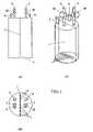
- FIGS. 1(A) , 1 (B), and 1 (C)are schematic views of one embodiment of a filled container of the present invention, in which FIG. 1(A) is a cross sectional view, FIG. 1(B) is a plan view, and FIG. 1(C) is a perspective view;
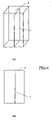
- FIGS. 2(A) and 2(B)are schematic views of one embodiment of a filled container of the present invention, in which FIG. 2(A) is a cross sectional view and FIG. 2(B) is a plan view;
- FIGS. 3(A) and 3(B)are schematic views of one embodiment of a filled container of the present invention, in which FIG. 3(A) is a cross sectional view and FIG. 3(B) is a plan view;
- FIGS. 4(A) and 4(B)are schematic views of one embodiment of a filled container of the present invention, in which FIG. 4(A) is a cross sectional view and FIG. 4(B) is a plan view;
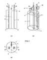
- FIGS. 5(A) and 5(B)are schematic views of one embodiment of a filled container of the present invention, in which FIG. 5(A) is a perspective view and FIG. 5(B) is a cross sectional view;
- FIGS. 6(A) and 6(B)are schematic views of one embodiment of a filled container of the present invention, in which FIG. 6(A) is a perspective view and FIG. 6(B) is a cross sectional view;
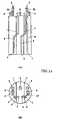
- FIGS. 7(A) , 7 (B), and 7 (C)are schematic views of one embodiment of a filled container of the present invention, in which FIG. 7(A) is a cross sectional view, FIG. 7(B) is a plan view, and FIG. 7(C) is a perspective view;
- FIGS. 8(A) , 8 (B), and 8 (C)are schematic views of one embodiment of a filled container of the present invention, in which FIG. 8(A) is a cross sectional view, FIG. 8(B) is a plan view, and FIG. 8(C) is a perspective view;
- FIGS. 9(A) and 9(B)are schematic views of one embodiment of a filled container of the present invention, in which FIG. 9(A) is a perspective view and FIG. 9(B) is a cross sectional view;
- FIGS. 10(A) and 10(B)are schematic views of one embodiment of a filled container of the present invention, in which FIG. 10(A) is a perspective view and FIG. 10(B) is a cross sectional view;
- FIGS. 11(A) and (B)are schematic views of one embodiment of a filled container of the present invention, in which FIG. 11(A) is a perspective view and FIG. 11(B) is a cross sectional view;
- FIGS. 12(A) , 12 (B), and 12 (C)are schematic views of one embodiment of a filled container of the present invention, in which FIG. 12(A) is a cross sectional view, FIG. 12(B) is a plan view, and FIG. 12(C) is a perspective view;
- FIGS. 13(A) , 13 (B), and 13 (C)are schematic views of one embodiment of a filled container of the present invention, in which FIG. 13(A) is a cross sectional view, FIG. 13(B) is a plan view, and FIG. 13(C) is a perspective view,
- FIGS. 14(A) and 14(B)are schematic views of one embodiment of a filled container of the present invention, in which FIG. 14(A) is a cross sectional view and FIG. 14(B) is a plan view;
- FIGS. 15(A) and 15(B)are schematic views of one embodiment of a filled container of the present invention, in which FIG. 15(A) is a cross sectional view and FIG. 15(B) is a plan view;
- FIGS. 16(A) and 16(B)are schematic views of one embodiment of a filled container of the present invention, in which FIG. 16(A) is a cross sectional view and FIG. 16(B) is a plan view;
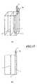
- FIG. 17is a perspective view of one embodiment of a filled container of the present invention.
- FIG. 18is a perspective view of one embodiment of a filled container of the present invention.
- FIG. 19is a perspective view of one embodiment of a filled container of the present invention.
- FIG. 20is a perspective view of one embodiment of a filled container of the present invention.
- FIGS. 21(A) and 21(B)are schematic views of one embodiment of a filled container of the present invention, in which FIG. 21(A) is a perspective view and FIG. 21(B) is a cross sectional view;
- FIGS. 22(A) and 22(B)are schematic views of one embodiment of a filled container of the present invention, in which FIG. 22(A) is a perspective view and FIG. 22(B) is a cross sectional view;
- FIGS. 23(A) and 23(B)are schematic views of one embodiment of a filled container of the present invention, in which FIG. 23(A) is a perspective view and FIG. 23(B) is a cross sectional view;
- FIGS. 24(A) and 24(B)are schematic views of one embodiment of a filled container of the present invention, in which FIG. 24(A) is a perspective view and FIG. 24(B) is a cross sectional view;
- FIGS. 25(A) and 25(B)are schematic views of one embodiment of a filled container of the present invention, in which FIG. 25(A) is a perspective view and FIG. 25(B) is a cross sectional view;
- FIGS. 26(A) and 26(B)are schematic views of one embodiment of a filled container of the present invention, in which FIG. 26(A) is a perspective view and FIG. 26(B) is a cross sectional view;
- FIGS. 27(A) and 27(B)are schematic views of one embodiment of a filled container of the present invention, in which FIG. 27(A) is a perspective view and FIG. 27(B) is a cross sectional view;
- FIGS. 28(A) , 28 (B), and 28 (C)are schematic views of a filled container used in Example 1 and Example 2, in which FIG. 28(A) is a cross sectional view, FIG. 28(B) is a plan view, and FIG. 28(C) is a perspective view;
- FIGS. 29(A) , 29 (B), and 29 (C)are schematic views of a filled container used in Example 3, in which FIG. 29(A) is a cross sectional view, FIG. 29(B) is a plan view and FIG. 29(C) is a perspective view;
- FIG. 30is a graph representing a result of the supply stability test of trimethylindium in Example 1 (representing the relation between used rate of supplied trimethylindium and supply amount of trimethylindium per hour);
- FIG. 31is a graph representing a result of the supply stability test of trimethylindium in Comparative example 1 (representing the relation between used rate of supplied trimethylindium and supply amount of trimethylindium per hour);
- FIG. 32is a graph representing a result of the supply stability test of trimethylindium in Example 2 (representing the relation between used rate of supplied trimethylindium and supply amount of trimethylindium per hour);
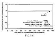
- FIG. 33is a graph representing a result of the supply stability test of trimethylindium in Example 3 (representing the relation between used rate of supplied trimethylindium and supply amount of trimethylindium per hour);
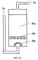
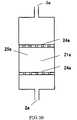
- FIG. 34is a schematic cross sectional view of a conventional filled container A
- FIG. 35is a schematic cross sectional view of a conventional filled container B
- FIG. 36is a schematic cross sectional view of a conventional filled container C.
- FIG. 37is a schematic cross sectional view of a conventional filled container D.
- the structure of the filled container of the present inventionis not particularly limited insofar as the interior space of the filled container is separated into a plurality of vertical compartments so as to allow carrier gas flow in each compartment.
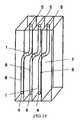
- FIGS. 1(A) to 4(B)each represent one exemplary embodiment of a solid organometallic compound-filled container of the present invention.
- the solid organometallic compound-filled container of the present inventionis constructed to have at least two partitioned compartments by separating the interior in the vertical direction with at least one partition ( 1 ). The space may be separated by the partition ( 1 ) in the manner as shown in FIGS. 1(A) to 4(B) , for example.
- the external form of the filled containermay be polygonal prism, including a triangle prism, quadratic prism, pentagonal prism, and hexagonal prism, as well as the cylinder as shown in FIGS. 1(A) to 4(B) .
- the solid organometallic compound-filled container of the present inventionhas a carrier gas inlet ( 2 ) that leads to one of the compartments formed in the filled container by separation with the partition ( 1 ) and a carrier gas outlet ( 3 ) that leads to the other of the compartments, and has a structure as shown in FIGS. 1(A) to 4(B) , for example.
- Carrier gasis introduced into the filled container filled with a solid organometallic compound via the carrier gas inlet ( 2 ), caused to flow in the filled container, discharged via the carrier gas outlet ( 3 ) in the form of gas that is saturated with the organometallic compound, and supplied to an MOCVD apparatus.
- the carrier gas inlet ( 2 ) and the carrier gas outlet ( 3 )may be disposed, for example, at the upper part of the filled container or at the side face of the filled container depending on the manner of separation of the space by the partition ( 1 ), the form of use of the filled container and the like.
- the partition ( 1 ) disposed inside the filled container of the present inventionhas an opening ( 4 ) which allows the carrier gas to flow from the carrier gas inlet ( 2 ) to the carrier gas outlet ( 3 ) through each compartment in the filled container.
- Examples of the partition ( 1 ) having such an opening ( 4 )include those having the structures as shown in FIGS. 5(A) through 6(B) .
- the position of the opening ( 4 )is not particularly limited insofar as it allows the carrier gas to sufficiently flow from the carrier gas inlet ( 2 ) to the carrier gas outlet ( 3 ) through the compartment filled with a solid organometallic compound, while allowing the filling solid organometallic compound to sufficiently contact with the carrier gas as well as not causing any trouble for stable supply of the organometallic compounds.
- the opening ( 4 ) for passage of the carrier gasis disposed in the lower part of the partition ( 1 ) so as to effectively bring the filling solid organometallic compound and the carrier gas into contact with each other to achieve saturation
- the opening ( 4 )is disposed at less than or equal to one-third, preferably one-fifth, and more preferably at less than or equal to one-tenth of the internal height of the container, from the internal bottom of the filled container.
- the opening ( 4 )is disposed in the upper part of the partition ( 1 )
- the opening ( 4 )is disposed at more than or equal to two-thirds, preferably at more than or equal to four-fifths, and more preferably at more than or equal to nine-tenths of the internal height of the container from the internal bottom of the filled container.
- the carrier gasis caused to flow in each compartment and discharged via the carrier gas outlet ( 3 ).
- Exemplary structures of the partition ( 1 ) having the opening ( 4 ) in the filled container of the present inventioninclude the structure shown in FIGS. 1(A) to 1(C) for a container having only one partition ( 1 ), the structure shown in FIGS. 2(A) and 2(B) for a container having two partitions ( 1 ), and the structures shown in FIGS. 3(A) , 3 (B) and 4 (A), 4 (B) for a container having three or more partitions ( 1 ).
- each of the carrier gas inlet ( 2 ) and the carrier gas outlet ( 3 )may have a flow channel ( 5 ) for letting the carrier gas flow in every compartment from the carrier gas inlet ( 2 ) to the carrier gas outlet ( 3 ) through the opening ( 4 ).
- the structures shown in FIGS. 7(A) through 8(C)are examples of a filled container in which each of the carrier gas inlet ( 2 ) and the carrier gas outlet ( 3 ) is provided with the flow channel ( 5 ).
- the flow channel ( 5 )may be a tubular member as shown in FIGS. 9(A) and 9(B) , or a member having flow channel lower openings ( 6 ) in the lower part of the structure formed by separating by the partition ( 1 ) as shown in FIGS. 10(A) , 10 (B), and 11 (A), 11 (B). Also the flow channel ( 5 ) may be a combination of a tubular member and the structure having flow channel lower openings ( 6 ) in the lower part of the structure formed by separating with the partition ( 1 ).
- the flow channel lower openings ( 6 ) of the flow channel ( 5 )are located at less than or equal to one-third, preferably at less than or equal to one-fifth, and more preferably at less than or equal to one-tenth of the internal height of the container from the internal bottom of the filled container.
- the state of the carrier gas in the filled container of the present inventionwill be described with reference to FIGS. 1(A) to 1(C) .
- the carrier gas introduced via the carrier gas inlet ( 2 )flows in the compartment having the carrier gas inlet ( 2 ).
- the carrier gas having flowed through each compartment via the opening ( 4 )is then discharged from the carrier gas outlet ( 3 ) and supplied to the MOCVD apparatus.
- the flow state of the carrier gaswas explained with reference to FIGS. 1(A) to 1(C) .
- the carrier gasflows via the openings ( 4 ) provided in each partition ( 1 ).
- the interior space of the filled containeris filled with the solid organometallic compound.
- a method of filling a solid organometallic compound-filled container of the present invention with the solid organometallic compoundconventionally known methods can be used as they are.
- introduction of a solid organometallic compound into a filled container by sublimationintroduction of an organometallic compound into the filled container in the form of saturated vapor in a carrier gas, and introduction of a liquid organometallic compound obtained by heating the organometallic compound to its melting point or higher temperature are examples.
- a charging port ( 9 )may be provided for filling the inside compartments of the filled container formed by the partition ( 1 ) with a solid organometallic compound.
- the charging port of the filled containercan be disposed, for example, in the upper part of the filled container as shown in FIGS. 1(A) to 4(B) .
- the carrier gas inlet ( 2 ) and/or the carrier gas outlet ( 3 )can function as the charging port ( 9 ) as well.
- the detached carrier gas inlet ( 2 ) and/or the carrier gas outlet ( 3 )can be connected with the filled container again by a connector ( 26 ) before use.
- the connector ( 26 ) that is detachable for forming the charging portis provided between the carrier gas inlet ( 2 ) and the filled container, with which the carrier gas inlet ( 2 ) and the filled container are connected again before use.
- the filled containermay or may not have the charging port depending on the filling method of a solid organometallic compound.
- the carrier gas inlet ( 2 ) and the carrier gas outlet ( 3 )may have a valve ( 22 ) that can be opened/closed. While the carrier gas flows, the valve ( 22 ) is opened, and while the organometallic compound is not supplied, the valve is usually closed to prevent the solid organometallic compound from being contaminated by the environment or from evaporating to the exterior of the filled container by sublimation.
- the filled container of the present inventionis designed so that the interior of the filled container is separated into a plurality of compartments by the partition ( 1 ), and the carrier gas introduced via the carrier gas inlet ( 2 ) passes through each compartment while contacting with the solid organometallic compound filling the container to flow to the carrier gas outlet ( 3 ).
- the partition ( 1 )By separating the interior of the container with the partition ( 1 ) to form a plurality of compartments as described above, the section area of each compartment is reduced and the carrier gas can desirably contact with the solid organometallic compound.
- the carrier gas introduced via the carrier gas inletmay be directed to flow in each of the vertical compartments in downward flow by carrier gas flow direction inverting means and discharged via the carrier gas outlet.
- the structure of the filled container having the above structure according to the present inventionis not particularly limited insofar as the interior space is separated into a plurality of vertical compartments, through which the carrier gas flows in downward flow.
- the carrier gas flow direction inverting means of the present inventioninverts the flow direction of the carrier gas flowing in one vertical compartment in downward flow and supplies the upper part of the next vertical compartment with the carrier gas in downward flow.
- Concrete examples of the carrier gas flow direction inverting meansinclude, but are not limited to, those having a communicating channel in a partition as shown in FIG. 13(A) to 20 , those having a partition formed by a communicating channel as shown in FIGS. 21(A) , 21 (B), and 22 (A), 22 (B), and those having a partition forming a communicating channel as shown in FIGS. 23(A) , 23 (B), and 24 (A), 24 (B).
- FIGS. 13(A) to 16(B)Examples of the solid organometallic compound-filled container of the present invention are shown in FIGS. 13(A) to 16(B) .
- the solid organometallic compound-filled container of the present inventionhas at least two compartments formed by separating the interior of the filled container in the vertical direction with at least one partition ( 1 ).
- the partition ( 1 )separates the space in the manner as shown in FIGS. 1(A) to 4(B) , for example.
- the external form of the filled containermay be polygonal prism, including a triangle prism, quadratic prism, pentagonal prism and hexagonal prism, as well as the cylinder as shown in FIGS. 13(A) to 16(B) .
- the solid organometallic compound-filled container of the present inventionhas the carrier gas inlet ( 2 ) that leads to one of the compartments formed in the filled container by separation with the partition ( 1 ) and the carrier gas outlet ( 3 ) that leads to the other of the compartments, and has a structure as shown in FIGS. 13(A) to 16(B) , for example.
- Carrier gasis introduced into the filled container filled with a solid organometallic compound via the carrier gas inlet ( 2 ) so as to flow in the filled container, and the gas saturated with the organometallic compounds is drawn out via the carrier gas outlet ( 3 ) to be supplied to an MOCVD apparatus.
- the carrier gas inlet ( 2 ) and the carrier gas outlet ( 3 )may be disposed, for example, at the upper part of the filled container or the side face of the filled container depending on the manner of separating the space by the partition ( 1 ), the form of use of the filled container and the like.
- the partition ( 1 ) disposed inside the filled container of the present inventionhas the communicating channel ( 6 ) having the lower opening ( 4 ) and the upper opening ( 5 ) for letting the carrier gas flow from the carrier gas inlet ( 2 ) to the carrier gas outlet ( 3 ) through each compartment in the filled container.
- the filled container of the present inventionalso has a structure such that the carrier gas introduced to the interior of the filled container is introduced via the lower opening ( 4 ) to the communicating channel ( 6 ) and then discharged via the upper opening ( 5 ), as shown in FIGS. 13(A) to 16(B) .
- the carrier gasflows in each compartment and is discharged via the carrier gas outlet ( 3 ).
- the filled container of the present inventionalso includes a discharging channel ( 8 ) having a lower opening ( 7 ) that discharges the carrier gas to the carrier gas outlet ( 3 ) from the lower part of the compartment having the carrier gas outlet ( 3 ), as shown in FIGS. 13(A) to 16(B) .
- exemplary structures of the communicating channel ( 6 ) and the discharging channel ( 8 )include the structure shown in FIGS. 13(A) to 13(C) for a container having only one partition ( 1 ), the structure shown in FIGS. 14(A) and 14(B) for a container having two partitions ( 1 ), and the structure shown in FIG. 15(A) , 15 (B), or 16 (A), 16 (B) for a container having three or more partitions ( 1 ).
- the communicating channel ( 6 )may be configured by one or a plurality of tubular members as shown in FIGS. 17 to 20 , for example.
- the carrier gasflows up in the discharging channel ( 8 ) from the lower opening ( 7 ) of the discharging channel ( 8 ) located near the lower part of the compartment having the carrier gas outlet ( 3 ) and is then discharged via the carrier gas outlet ( 3 ) and supplied to the MOCVD apparatus.
- the flow state of the carrier gashas been explained according to FIGS. 13(A) to 13(C) , however, when the interior of the filled container is separated into three or more compartments, as shown in FIGS. 14(A) to 16(B) , the carrier gas flows down from top to bottom in each compartment through the communicating channel ( 6 ) provided at each partition ( 1 ).
- FIGS. 21(A) to 24(B)A similar effect is achieved by employing a structure wherein the partition ( 1 ) also serves as the communicating channel ( 6 ) as shown in FIGS. 21(A) to 24(B) .
- Containers having the following structuresare examples of such a structure.
- a plurality of tubular structuresare aligned so as to adjoin each other along the length thereof while each interval is closed by the neighboring tubular structure.
- FIGS. 22(A) and 22(B)each interval between adjacent tubular structures in FIGS. 21(A) and 21(B) is closed by the partition ( 1 ).
- An openingis provided in the lower part of the tubular structure on the side of the upstream compartment in respect of the carrier gas flow direction to serve as the lower opening ( 4 ), and an opening is provided in the upper part of the tubular structure on the side of the downstream compartment to serve as the upper opening ( 5 ).
- two partitions ( 1 )are provided, wherein one partition ( 1 ) on the side of the upstream compartment in respect of the carrier gas flow direction is formed with openings in its lower part to serve as the lower opening ( 4 ), and the other partition ( 1 ) on the side of the downstream compartment is formed with openings in its upper part to serve as the upper opening ( 5 ).
- the communicating channel ( 6 )may be of a tubular structure or of a structure combined with the structure wherein the partition ( 1 ) also severs as the communicating channel ( 6 ).
- the discharging channel ( 8 ) having the lower opening ( 7 ) that discharges the carrier gas to the carrier gas outlet ( 3 ) from the lower part of the compartment having the carrier gas outlet ( 3 )may also have a tubular structure having an opening in the lower part as shown in FIGS. 25(A) and 25(B) , or a structure as shown in FIGS. 26(A) , 26 (B), or FIGS. 27(A) , 27 (B) wherein the lower opening ( 7 ) is provided in the lower part of the structure separated by the partition ( 1 ) and the like.
- the discharging channel ( 8 )may be of the tubular structure as described above or the structure combined with the structure having the lower opening ( 7 ) in the lower part of the structure separated by the partition ( 1 ).
- the positions of the upper opening ( 5 ) and the lower opening ( 4 )are not particularly limited insofar as the carrier gas can sufficiently flow from the carrier gas inlet ( 2 ) to the carrier gas outlet ( 3 ) through the compartment filled with the solid organometallic compound, through the communicating channel ( 6 ) and through the discharging channel ( 8 ) having the lower opening ( 7 ) from which the carrier gas is discharged to the carrier gas outlet ( 3 ), and the filling solid organometallic compound can sufficiently contact with the carrier gas, wherein stable supply of the organometallic compounds is not disturbed.
- the lower opening ( 4 )be positioned at less than or equal to one third, preferably at less than or equal to one fifth, more preferably at less than or equal to one tenth of the height of the container from the internal bottom of the filled container, and the upper opening ( 5 ) be positioned at more than or equal to two-thirds, preferably at more than or equal to four-fifths, more preferably at more than or equal to nine tenths of the height of the container from the internal bottom of the filled container.
- the lower opening ( 7 )be positioned at less than or equal to one third, preferably at less than or equal to one fifth, more preferably at less than or equal to one tenth of the height of the container from the internal bottom of the filled container.
- the interior space of the filled containeris filled with the solid organometallic compound.
- a method of filling a solid organometallic compound-filled container of the present invention with the solid organometallic compoundconventionally known methods can be used as they are.
- introduction of a solid organometallic compound into a filled container by sublimationintroduction of an organometallic compound into the filled container in the form of saturated vapor in the carrier gas, and introduction of a liquid organometallic compound obtained by heating the organometallic compound to its melting point or higher temperature are examples.
- a charging port ( 9 )may be provided for filling the inside compartments of the filled container formed by the partition ( 1 ) with a solid organometallic compound.
- the charging port of the filled containercan be disposed, for example, in the upper part of the filled container as shown in FIGS. 13(A) to 16(C) .
- the carrier gas inlet ( 2 ) and/or the carrier gas outlet ( 3 )can function also as the charging port ( 9 ).
- the detached carrier gas inlet ( 2 ) and/or the carrier gas outlet ( 3 )can be connected again with the filled container by a connector ( 26 ) before use.
- the discharging channel ( 8 ) to be connected to the carrier gas outlet ( 3 )is detachable, filling with the solid organometallic compound can be facilitated.
- the connector ( 26 ) that is detachable for forming the charging portis provided between the carrier gas inlet ( 2 ) and the filled container, with which connector the carrier gas inlet ( 2 ) and the filled container are connected again before use.
- the filled containermay or may not have the charging port depending on the filling method of the solid organometallic compound.
- the carrier gas inlet ( 2 ) and the carrier gas outlet ( 3 )may have a valve ( 22 ) that can be opened/closed. While the carrier gas flows, the valve ( 22 ) is opened, and while the organometallic compound is not supplied, the valve is usually closed to prevent the solid organometallic compound from being contaminated by the environment or from evaporating to the exterior of the filled container by sublimation.
- the filled container of the present inventionis designed so that the interior of the filled container is separated into a plurality of compartments by the partition ( 1 ), and the carrier gas introduced via the carrier gas inlet ( 2 ) passes through the solid organometallic compound filling each compartment of the container from top to bottom thereof in every compartment to flow to the carrier gas outlet ( 3 ).
- the partition ( 1 )By separating the interior of the container with the partition ( 1 ) to form a plurality of compartments as described above, the sectional area of each compartment is reduced and the carrier gas can desirably contact with the solid organometallic compound.
- solid organometallic compound that can be used for filling the filled container of the present inventionnot only the known solid organometallic compounds that have been used in a conventional filled container, but also other solid organometallic compounds are applicable, insofar as they have enough saturated vapor pressure to achieve the desired supply to the carrier gas under the temperature and pressure used for supply by means of the carrier gas, and are in a solid state under the supply conditions.
- Representative examples of these solid organometallic compoundsinclude alkyl metal compounds, metallocene compounds, ⁇ -diketone complexes, and adduct compounds.
- alkyl metal compoundssuch as trimethylindium, dimethylchloroindium, triphenylaluminum, triphenylbismuth, and tert-butyllithium
- metallocene compoundssuch as cyclopentadienylindium, bis(cyclopentadienyl)magnesium, bis(cyclopentadienyl)manganese, and ferrocene
- ⁇ -diketone complexessuch as barium acetylacetonato complex, strontium acetylacetonato complex, copper acetylacetonato complex, calcium acetylacetonato complex, barium dipivaloyl methanato complex, strontium dipivaloyl methanato complex, copper dipivaloyl methanato complex, yttrium dipivaloyl methanato complex, and calcium dipivaloyl methanato complex; and adduct compounds such as
- any conditions that are conventionally used in a filled containercan be used without modification, and conditions that allow stable supply of the solid organometallic compound to the MOCVD apparatus over a long term can be used without any restriction.
- Any of elevated pressures, normal pressures, and reduced pressuresare available, however, pressures around normal pressures to reduced pressures are usually employed.
- any conditions that are conventionally used in a filled containercan be used without modification, and the conditions under which a commonly used solid organometallic compound has a saturated vapor pressure that is sufficient to supply the carrier gas as desired and in which the solid organometallic compound is solid in the supply condition are possible.
- any kinds of carrier gas that are conventionally used in filled containerscan be used, including inert gases such as nitrogen, argon, and helium, and hydrogen gas.
- packing materialsthat are used together with a solid organometallic compound for filling the known filled container can be used.
- packing materialsthose made of stainless steel, glass, ceramics, fluorine plastic, and the like are used, and those made of stainless steel are preferably used.
- the packing materialmay have round, square, cylinder, coil, spring, globular and other shapes, and examples of these include various packing for distillation such as Dixon packing, Helipack, Fenske, and the like. Also, fibrous packing materials may be used.
- packing materialscan be used together with the solid organometallic compound for filling the filled container by a know method in the filled container of the present invention.
- the filled container of the present inventionis used as a filled container not only for the solid organometallic compound but also for general solid substances such as solid inorganic compounds, solid organic compounds, or solid metals having different vapor pressures. Therefore, the filled container of the present invention can be used for drawing out other solid substances in place of the solid organometallic compound in the form of saturated gas by using a carrier gas.
- the supply stability testwas conducted in the manner below.
- a filled container formed of SUS and having an outer diameter of 76.0 mm ⁇ as shown in FIG. 7(A) to 7(C)was filled with 400 g of trimethylindium and 647 g of stainless packing material via the charging port ( 9 ).
- the carrier gas outlet ( 3 )was connected to a trap for trapping trimethylindium that was cooled on dry ice/methanol. Piping that connects the carrier gas outlet ( 3 ) and the trap cooled on dry ice/methanol was heated so that trimethylindium would not precipitate in this piping.
- the filled container filled with trimethylindium and the packing materialwas placed in a temperature controlled bath set at 25° C., 500 cc per minute of nitrogen gas was fed via the carrier gas inlet ( 2 ) of the filled container under the condition that the internal pressure of the appliance system for the supply stability test was adjusted to nearly atmospheric pressure, and the weight of trimethylindium trapped in the trap cooled on dry ice/methanol was measured every eight hours. Also the gas concentration of the gas phase of carrier gas containing vapor of trimethylindium was determined by using an ultrasonic type gas densitometer (“EPISON”TM available from Thomas Swan Scientific Equipment Ltd.).
- FIG. 30The result is shown in FIG. 30 .
- the vertical axisrepresents supplied amount per hour of trimethylindium
- the horizontal axisrepresents used rate of the supplied trimethylindium in % by weight.
- the filled container shown in FIGS. 7(A) to 7(C)makes it possible to stably supply a solid organometallic compound at a constant concentration, and enables the used rate of the solid organometallic compound to be increased under the condition where stable supply speed is achieved. As a result, it is possible to elongate the period during which the solid organometallic compound can be stably supplied by using the filled container of the present invention.
- a conventional filled container A shown in FIG. 34was filled with trimethylindium as a solid organometallic compound and supply stability of the solid organometallic compound was examined in the same manner as described in Example 1. The result is shown in FIG. 31 .
- the result of the supply stability testdemonstrated that when the conventional filled container A shown in FIG. 34 was used, the supply speed of trimethylindium was stable up to the used rate of 35% by weight.
- the supply stability testwas conducted in the following manner.
- a filled container formed of SUS and having an outer diameter of 60.5 mm ⁇ as shown in FIGS. 28(A) to 28(C)was filled with 200 g of trimethylindium and 260 g of stainless packing material via the charging port ( 9 ).
- the carrier gas inlet ( 2 )was detached from the filled container at the connector ( 26 ) for giving the charging port ( 9 ).
- the carrier gas outlet ( 3 )was connected to a trap for trapping trimethylindium that was cooled on dry ice/methanol. Piping that connects the carrier gas outlet ( 3 ) and the trap cooled on dry ice/methanol was heated so that trimethylindium would not precipitate in this piping.
- the filled container filled with trimethylindium and the packing materialwas placed in a temperature controlled bath set at 25° C., 500 cc per minute of nitrogen gas was introduced via the carrier gas inlet ( 2 ) of the filled container under the condition that the internal pressure of the appliance system for the supply stability test was adjusted to nearly atmospheric pressure, and the weight of trimethylindium trapped in the trap cooled on dry ice/methanol was measured every eight hours.
- the gas concentration of the gas phase of carrier gas containing vapor of trimethylindiumwas determined by using a ultrasonic type gas densitometer (“EPISON”TM available from Thomas Swan Scientific Equipment Ltd.).
- FIG. 32The result is shown in FIG. 32 .
- the vertical axisrepresents supplied amount per hour of trimethylindium
- the horizontal axisrepresents used rate of the supplied trimethylindium in % by weight.
- the filled container shown in FIGS. 28(A) to 28(C)makes it possible to stably supply a solid organometallic compound at a constant concentration, and enables the used rate of the solid organometallic compound to be increased under the condition where stable supply speed is achieved. As a result, it is possible to elongate the period during which the solid organometallic compound can be stably supplied by using the filled container of the present invention.
- the supply stability testwas conducted in the following manner.
- a filled container formed of SUS and having an outer diameter of 114 mm ⁇ as shown in FIG. 29(A) to 29(C)was filled with 1000 g of trimethylindium and 517 g of stainless packing material via the charging port ( 9 ).
- the carrier gas inlet ( 2 )was detached from the filled container at the connector ( 26 ) for using the charging port ( 9 ).
- the carrier gas outlet ( 3 )was connected to a trap for trapping trimethylindium that was cooled on dry ice/methanol. Piping that connects the carrier gas outlet ( 3 ) and the trap cooled on dry ice/methanol was heated so that trimethylindium would not precipitate in this piping.
- the filled container filled with trimethylindium and the packing materialwas placed in a temperature controlled bath set at 25° C., 1000 cc per minute of nitrogen gas was introduced via the carrier gas inlet ( 2 ) of the filled container under the condition that the internal pressure of the appliance system for the supply stability test was reduced to about 66.6 kPa (500 torr), and the weight of trimethylindium trapped in the trap cooled on dry ice/methanol was measured every eight hours.
- the gas concentration of the gas phase of carrier gas containing vapor of trimethylindiumwas determined by using an ultrasonic type gas densitometer (“EPISON”TM available from Thomas Swan Scientific Equipment Ltd.).
- FIG. 33The result is shown in FIG. 33 .
- the vertical axisrepresents supplied amount per hour of trimethylindium
- the horizontal axisrepresents used rate of the supplied trimethylindium in % by weight.
- the filled container shown in FIGS. 29(A) to 29(C)makes it possible to stably supply a solid organometallic compound at a constant concentration, and enables the used rate of the solid organometallic compound to be increased under the condition where stable supply speed is achieved. As a result, it is possible to elongate the period during which the solid organometallic compound can be stably supplied by using the filled container of the present invention.
- a conventional filled container A shown in FIG. 34was filled with trimethylindium as a solid organometallic compound and supply stability of the solid organometallic compound was examined in the same manner as described in Example 2.
- the result of the supply stability testdemonstrated that when the conventional filled container A shown in FIG. 34 was used, the supply speed of trimethylindium was stable up to the used rate of 52% by weight.
- an apparatus for vapor phase epitaxial growthsuch as an MOCVD apparatus with a solid organometallic compound over a long term without increasing the outer size of the filled container compared to the conventional filled container.
Landscapes
- Chemical & Material Sciences (AREA)
- General Chemical & Material Sciences (AREA)
- Chemical Kinetics & Catalysis (AREA)
- Engineering & Computer Science (AREA)
- Materials Engineering (AREA)
- Metallurgy (AREA)
- Organic Chemistry (AREA)
- Mechanical Engineering (AREA)
- Crystallography & Structural Chemistry (AREA)
- Chemical Vapour Deposition (AREA)
Abstract
Description
1. Field of the Invention
The present invention relates to a solid organometallic compound-filled container and a filling method thereof. More specifically, the present invention relates to a solid organometallic compound-filled container and a filling method thereof capable of stably supplying an apparatus for vapor phase epitaxial growth with a constant concentration of a solid organometallic compound over a long term. This solid organometallic compound is a material for use in a vapor phase epitaxial growth technique based on Metalorganic Chemical Vapor Deposition (hereinafter, abbreviated as “MOCVD”) method or the like which is used in the manufacture of electronics materials such as compound semiconductors.
2. Description of the Related Art
Organometallic compounds have broad use as materials in manufacture of electronics materials.
In the manufacture of electronics material using organometallic compounds, vapor phase epitaxial growth based on the MOCVD method or the like has often been used in recent years. For example, a thin film of compound semiconductor is manufactured by the MOCVD method using an organometallic compound such as trimethylaluminum, trimethylgallium, and trimethylindium as a material.
When such an organometallic compound is used in the MOCVD method and the organometallic compound is solid in the condition of the MOCVD method, usually, a filled container A having a carrier gas inlet (2a) and a carrier gas outlet (3a) as shown inFIG. 34 is filled with the organometallic compound, a carrier gas such as hydrogen gas is introduced into the container via the carrier gas inlet (2a), and the organometallic compound is drawn out as a gas in which the organometallic compound is saturated in the carrier gas via the carrier gas outlet (3a) to be supplied to the MOCVD apparatus.
When the organometallic compound is solid at the temperature that is used in the supplying step, a flow channel is formed in the filled container A where the carrier gas passes through without sufficiently contacting with the solid organometallic compound, making it difficult to keep the carrier gas and the solid organometallic compound in contact with each other in a uniform condition. Therefore, it is difficult to stably supply the MOCVD apparatus with the solid organometallic compound from the filled container A at a constant concentration over a long term. When the solid organometallic compound is supplied according to the aforementioned method using the carrier gas, the ratio of the amount of solid organometallic compound that can be stably supplied to the MOCVD apparatus relative to the filling amount of solid organometallic compound decreases, as the amount of solid organometallic compound to fill the filled container A increases, so that the amount of the solid organometallic compound remaining in the filled container increases, and effective use of the solid organometallic compound is disabled.
For solving these problems, various proposals have been made concerning the method of filling the filled container A with the solid organometallic compound. For example, a method of filling a filled container with a solid organometallic compound together with a filling material is proposed in Japanese Patent Publication No. Hei 5-39915, Japanese Patent Publication No. Hei 6-20051, Japanese Patent Laid-Open Publication No. Hei 7-58023, Japanese Patent Laid-Open Publication No. Hei 8-250440, Japanese Patent Laid-Open Publication No. Hei 8-299778, and the like. For example, a method of filling a filled container A with an inert carrier covered with a solid organometallic compound is proposed in Published Japanese Patent No. 2651530 and the like.
In addition to these proposals, various proposals concerning structure of a filled container itself to be filled with a solid organometallic compound have been made to solve the above-mentioned problems. For example, a filled container B having a diffuser (20a) for uniformizing gas disposed at the carrier gas inlet as shown inFIG. 35 to allow the carrier gas to uniformly flow with respect to the solid organometallic compound is proposed in Japanese Patent Publication No. Hei 2-124796 and the like.
Furthermore, a filled container C having a solid organometallic compound chamber (21a) having air permeability as shown inFIG. 36 is proposed, for example, in Japanese Patent Laid-Open Publication No. Hei 10-223540 and the like.
Furthermore, a filled container (hereinafter referred to as filled container D) in which a porous inlet chamber as shown inFIG. 37 serves as a filled region for solid organometallic compound is proposed, for example, in Japanese Patent Laid-Open Publication No. 2002-83777 and the like.
As shown inFIG. 34 , the conventional filled container A has a carrier gas inlet (2a) and a carrier gas outlet (3a) in a single container, and has a flow channel (8a) implemented by a dip tube with a lower opening (7a) which extends from the lower part of the carrier gas outlet to the bottom of the filled container A within the filled container. The present inventor carried out examination to find that when the filled container A having the structure as shown inFIG. 34 was used, in supplying a solid organometallic compound to the MOCVD apparatus using the carrier gas, the longer the supply period of the organometallic compound by the carrier gas, the more the supply amount of the organometallic compound in the carrier gas decreased in a gradual manner. In particular, the effect of stably supplying the solid organometallic compound was significantly impaired when the filling amount of the solid organometallic compound was increased, or the flow rate of the carrier gas was increased. Therefore, the filled container A does not achieve sufficient effect to stably supply the MOCVD apparatus with the solid organometallic compound over a long term.
Also, various filled containers that have been proposed other than that shown inFIG. 34 have a problem in that they are still not satisfactory in stably supplying the MOCVD apparatus with the solid organometallic compound over a long term in the method using carrier gas, or that the outer size of the filled container is significantly large.
As described above, the conventional filled containers for solid organometallic compound are faced with various problems, and there is a need for improving the supply stability of the solid organometallic compound and preventing the filled container from having a significantly large outer size.
The present invention solves the above-mentioned problems, and relates to a novel filled container capable of stably supplying an apparatus for vapor phase epitaxial growth such as an MOCVD apparatus with a solid organometallic compound at a constant concentration over a long term, and a method of filling the filled container with the solid organometallic compound.
For solving the aforementioned problems, the inventors carried out studies and found that by adopting a novel structure having the features as recited below to the internal structure of the filled container, it is possible to stably supply an apparatus for vapor phase epitaxial growth such as an MOCVD apparatus with a solid organometallic compound at a constant concentration over a long term without significantly increasing the outer size compared to the conventionally known filled containers and to increase the period during which the solid organometallic compound is stably supplied.
More specifically, the present invention provides a solid organometallic compound-filled container having a carrier gas inlet and a carrier gas outlet, wherein an interior of the filled container is separated into a plurality of vertical compartments, and a carrier gas introduced via the carrier gas inlet flows through each of the vertical compartments and is then discharged via the carrier gas outlet.
More specifically, the present invention provides a solid organometallic compound-filled container meeting the following requirements (a) to (c).
In a solid organometallic compound-filled container,
(a) an interior of the filled container is separated by at least one partition in a vertical direction, whereby the interior of the filled container is separated into at least two compartments;
(b) the compartments formed in the filled container by separating the interior with the partition includes a compartment having a carrier gas inlet and a compartment having a carrier gas outlet; and
(c) the partition inside the filled container includes a partition having an opening that allows the carrier gas to flow from the carrier gas inlet through each of the compartments inside the filled container to the carrier gas outlet.
According to a method of filling a solid organometallic compound-filled container of the present invention with a solid organometallic compound, in the aforementioned solid organometallic compound-filled container meeting the requirements (a) to (c), when the opening is disposed in a lower part of the partition, the opening is disposed at a point lower than or equal to one third of an internal height of the container from an internal bottom of the filled container. When the opening is disposed in an upper part of the partition, the opening is disposed at more than or equal to two thirds of the internal height of the container from the internal bottom of the filled container.
Furthermore, in the solid organometallic-filled container of the invention meeting the requirements (a) to (c), the filled container has a charging port for filling the solid organometallic compound into the compartment inside the filled container formed by separating the interior by the partition.
The present invention also provides a solid organometallic compound-filled container having a carrier gas inlet and a carrier gas outlet in which the interior of the filled container is separated into a plurality of vertical compartments and the carrier gas introduced via the carrier gas inlet flows through each of the vertical compartments and is then discharged via the carrier gas outlet. The carrier gas introduced via the carrier gas inlet is directed to flow downward through each of the vertical compartments and leave via the carrier gas outlet by carrier gas flow direction inverting means.
More specifically, the present invention provides the solid organometallic compound-filled container so as to meet the following requirements (d) to (h).
In the aforementioned solid organometallic compound-filled container,
(d) the interior of the filled container is separated by at least one partition in the vertical direction, whereby the interior of the filled container is separated into at least two compartments;
(e) the compartments formed in the filled container by separating the interior by the partition include a compartment having the carrier gas inlet and a compartment having the carrier gas outlet;
(f) the partition inside the filled container has a communicating channel with a lower opening and an upper opening that allows the carrier gas to flow from the carrier gas inlet through each of the compartments inside the filled container to the carrier gas outlet;
(g) in the communicating channel, the carrier gas introduced into the interior of the filled container is introduced via the lower opening and discharged via the upper opening of the communicating channel; and
(h) the filled container has a discharging channel having a lower opening for discharging the carrier gas from the lower part of the compartment having the carrier gas outlet via the carrier gas outlet.
In the solid organometallic-filled container of the present invention meeting the requirements of (d) to (h), in the aforementioned communicating channel, the lower opening of the communicating channel is disposed at less than or equal to one third of the internal height of the container from the internal bottom of the filled container, the upper opening of the communicating channel is disposed at more than or equal to two thirds of the internal height of the container from the internal bottom of the filled container, and in the discharging channel, the lower opening of the discharging channel is disposed at less than or equal to one third of the internal height of the container from the internal bottom of the filled container.
Furthermore, in the solid organometallic-filled container of the invention meeting the requirements (d) to (h), the filled container may have a charging port for filling the compartment formed in the filled container by separating the interior by the partition with the solid organometallic compound.
In the solid organometallic compound-filled container of the present invention, trimethylindium may be used as the solid organometallic compound.
The present invention also provides a solid organometallic compound filling method, wherein the filled container of the present invention is filled with a solid organometallic compound.
According to the present invention, in the solid organometallic compound-filled container, by vertically separating the interior of the filled container with a partition into a plurality of compartments to allow the carrier gas flow through each compartment, it is possible to stably supply an apparatus for vapor epitaxial growth such as an MOCVD apparatus with a solid organometallic compound over a long term without increasing the outer size compared to the conventional filled container.
The structure of the filled container of the present invention is not particularly limited insofar as the interior space of the filled container is separated into a plurality of vertical compartments so as to allow carrier gas flow in each compartment.
The solid organometallic compound-filled container and the method of filling the filled container according to the present invention will now be described in more detail with reference to the accompanying drawings.
The external form of the filled container may be polygonal prism, including a triangle prism, quadratic prism, pentagonal prism, and hexagonal prism, as well as the cylinder as shown inFIGS. 1(A) to 4(B) .
Furthermore, the solid organometallic compound-filled container of the present invention has a carrier gas inlet (2) that leads to one of the compartments formed in the filled container by separation with the partition (1) and a carrier gas outlet (3) that leads to the other of the compartments, and has a structure as shown inFIGS. 1(A) to 4(B) , for example. Carrier gas is introduced into the filled container filled with a solid organometallic compound via the carrier gas inlet (2), caused to flow in the filled container, discharged via the carrier gas outlet (3) in the form of gas that is saturated with the organometallic compound, and supplied to an MOCVD apparatus. The carrier gas inlet (2) and the carrier gas outlet (3) may be disposed, for example, at the upper part of the filled container or at the side face of the filled container depending on the manner of separation of the space by the partition (1), the form of use of the filled container and the like.
The partition (1) disposed inside the filled container of the present invention, as shown inFIGS. 1(A) to 4(B) , has an opening (4) which allows the carrier gas to flow from the carrier gas inlet (2) to the carrier gas outlet (3) through each compartment in the filled container.
Examples of the partition (1) having such an opening (4) include those having the structures as shown inFIGS. 5(A) through 6(B) .
The position of the opening (4) is not particularly limited insofar as it allows the carrier gas to sufficiently flow from the carrier gas inlet (2) to the carrier gas outlet (3) through the compartment filled with a solid organometallic compound, while allowing the filling solid organometallic compound to sufficiently contact with the carrier gas as well as not causing any trouble for stable supply of the organometallic compounds. In particular, when the opening (4) for passage of the carrier gas is disposed in the lower part of the partition (1) so as to effectively bring the filling solid organometallic compound and the carrier gas into contact with each other to achieve saturation, the opening (4) is disposed at less than or equal to one-third, preferably one-fifth, and more preferably at less than or equal to one-tenth of the internal height of the container, from the internal bottom of the filled container. When the opening (4) is disposed in the upper part of the partition (1), the opening (4) is disposed at more than or equal to two-thirds, preferably at more than or equal to four-fifths, and more preferably at more than or equal to nine-tenths of the internal height of the container from the internal bottom of the filled container.
Owing to the above structure, in the filled container of the present invention, the carrier gas is caused to flow in each compartment and discharged via the carrier gas outlet (3).
Exemplary structures of the partition (1) having the opening (4) in the filled container of the present invention include the structure shown inFIGS. 1(A) to 1(C) for a container having only one partition (1), the structure shown inFIGS. 2(A) and 2(B) for a container having two partitions (1), and the structures shown inFIGS. 3(A) ,3(B) and4(A),4(B) for a container having three or more partitions (1).
Furthermore, depending on the position of the opening (4) provided in the partition (1), each of the carrier gas inlet (2) and the carrier gas outlet (3) may have a flow channel (5) for letting the carrier gas flow in every compartment from the carrier gas inlet (2) to the carrier gas outlet (3) through the opening (4). The structures shown inFIGS. 7(A) through 8(C) are examples of a filled container in which each of the carrier gas inlet (2) and the carrier gas outlet (3) is provided with the flow channel (5).
The flow channel (5) may be a tubular member as shown inFIGS. 9(A) and 9(B) , or a member having flow channel lower openings (6) in the lower part of the structure formed by separating by the partition (1) as shown inFIGS. 10(A) ,10(B), and11(A),11(B). Also the flow channel (5) may be a combination of a tubular member and the structure having flow channel lower openings (6) in the lower part of the structure formed by separating with the partition (1).
Desirably the flow channel lower openings (6) of the flow channel (5) are located at less than or equal to one-third, preferably at less than or equal to one-fifth, and more preferably at less than or equal to one-tenth of the internal height of the container from the internal bottom of the filled container.
The state of the carrier gas in the filled container of the present invention will be described with reference toFIGS. 1(A) to 1(C) . First, the carrier gas introduced via the carrier gas inlet (2) flows in the compartment having the carrier gas inlet (2). The carrier gas having flowed through each compartment via the opening (4) is then discharged from the carrier gas outlet (3) and supplied to the MOCVD apparatus. The flow state of the carrier gas was explained with reference toFIGS. 1(A) to 1(C) . However, when the interior of the filled container is partitioned into three or more compartments as shown inFIGS. 2(A) to 4(B) , the carrier gas flows via the openings (4) provided in each partition (1).
In this flow state, when each of the carrier gas inlet (2) and the carrier gas outlet (3) has the flow channel (5) as shown inFIGS. 7(A) through 7(C) , the carrier gas introduced via the carrier gas inlet (2) flows in the flow channel (5) and then flows in the compartment having the carrier gas inlet (2). After flowing in each compartment via the opening (4) and flowing in the flow channel (5) having the carrier gas outlet (3), the carrier gas is discharged via the carrier gas outlet (3) and supplied to the MOCVD apparatus.
When the filled container of the present invention is filled with a solid organometallic compound and used for supplying the MOCVD apparatus with the solid organometallic compound, the interior space of the filled container is filled with the solid organometallic compound.
As a method of filling a solid organometallic compound-filled container of the present invention with the solid organometallic compound, conventionally known methods can be used as they are. As such conventional filling methods, introduction of a solid organometallic compound into a filled container by sublimation, introduction of an organometallic compound into the filled container in the form of saturated vapor in a carrier gas, and introduction of a liquid organometallic compound obtained by heating the organometallic compound to its melting point or higher temperature are examples.
Furthermore, in the solid organometallic compound-filled container of the present invention, a charging port (9) may be provided for filling the inside compartments of the filled container formed by the partition (1) with a solid organometallic compound. By providing this charging port (9), it becomes possible to introduce the solid organometallic compound in the solid form. In the present invention, the charging port of the filled container can be disposed, for example, in the upper part of the filled container as shown inFIGS. 1(A) to 4(B) . By designing the carrier gas inlet (2) and/or the carrier gas outlet (3) to be detachable from the filled container, these carrier gas inlet (2) and/or carrier gas outlet (3) can function as the charging port (9) as well. The detached carrier gas inlet (2) and/or the carrier gas outlet (3) can be connected with the filled container again by a connector (26) before use. In one exemplary structure shown inFIGS. 12(A) through 12(C) , the connector (26) that is detachable for forming the charging port is provided between the carrier gas inlet (2) and the filled container, with which the carrier gas inlet (2) and the filled container are connected again before use.
The filled container may or may not have the charging port depending on the filling method of a solid organometallic compound.
In the filled container of the present invention, as shown inFIGS. 1(A) to 4(B) , for example, the carrier gas inlet (2) and the carrier gas outlet (3) may have a valve (22) that can be opened/closed. While the carrier gas flows, the valve (22) is opened, and while the organometallic compound is not supplied, the valve is usually closed to prevent the solid organometallic compound from being contaminated by the environment or from evaporating to the exterior of the filled container by sublimation.
In brief, the filled container of the present invention is designed so that the interior of the filled container is separated into a plurality of compartments by the partition (1), and the carrier gas introduced via the carrier gas inlet (2) passes through each compartment while contacting with the solid organometallic compound filling the container to flow to the carrier gas outlet (3). By separating the interior of the container with the partition (1) to form a plurality of compartments as described above, the section area of each compartment is reduced and the carrier gas can desirably contact with the solid organometallic compound. Accordingly, it is possible to keep the contact state of the carrier gas and the solid organometallic compound uniform without causing formation of a flow channel as is the case in the conventional art, so that it is possible to stably supply the MOCVD apparatus with the solid organometallic compound from the filled container at a constant concentration over a long term by the carrier gas.
According to the present invention, in the solid organometallic compound-filled container having the carrier gas inlet and the carrier gas outlet, wherein the interior of the filled container is separated into a plurality of vertical compartments, and the carrier gas introduced via the carrier gas inlet flows in each of the vertical compartments and is then discharged via the carrier gas outlet, the carrier gas introduced via the carrier gas inlet may be directed to flow in each of the vertical compartments in downward flow by carrier gas flow direction inverting means and discharged via the carrier gas outlet.
The structure of the filled container having the above structure according to the present invention is not particularly limited insofar as the interior space is separated into a plurality of vertical compartments, through which the carrier gas flows in downward flow.
The carrier gas flow direction inverting means of the present invention inverts the flow direction of the carrier gas flowing in one vertical compartment in downward flow and supplies the upper part of the next vertical compartment with the carrier gas in downward flow. Concrete examples of the carrier gas flow direction inverting means include, but are not limited to, those having a communicating channel in a partition as shown inFIG. 13(A) to 20 , those having a partition formed by a communicating channel as shown inFIGS. 21(A) ,21(B), and22(A),22(B), and those having a partition forming a communicating channel as shown inFIGS. 23(A) ,23(B), and24(A),24(B).
The solid organometallic compound-filled container of the present invention and its filling method will be described in more detail with reference to the drawings.
Examples of the solid organometallic compound-filled container of the present invention are shown inFIGS. 13(A) to 16(B) . As shown inFIGS. 13(A) to 16(B) , the solid organometallic compound-filled container of the present invention has at least two compartments formed by separating the interior of the filled container in the vertical direction with at least one partition (1). The partition (1) separates the space in the manner as shown inFIGS. 1(A) to 4(B) , for example.
The external form of the filled container may be polygonal prism, including a triangle prism, quadratic prism, pentagonal prism and hexagonal prism, as well as the cylinder as shown inFIGS. 13(A) to 16(B) .
Furthermore, the solid organometallic compound-filled container of the present invention has the carrier gas inlet (2) that leads to one of the compartments formed in the filled container by separation with the partition (1) and the carrier gas outlet (3) that leads to the other of the compartments, and has a structure as shown inFIGS. 13(A) to 16(B) , for example. Carrier gas is introduced into the filled container filled with a solid organometallic compound via the carrier gas inlet (2) so as to flow in the filled container, and the gas saturated with the organometallic compounds is drawn out via the carrier gas outlet (3) to be supplied to an MOCVD apparatus. The carrier gas inlet (2) and the carrier gas outlet (3) may be disposed, for example, at the upper part of the filled container or the side face of the filled container depending on the manner of separating the space by the partition (1), the form of use of the filled container and the like.
The partition (1) disposed inside the filled container of the present invention, as shown inFIGS. 13(A) to 16(B) , has the communicating channel (6) having the lower opening (4) and the upper opening (5) for letting the carrier gas flow from the carrier gas inlet (2) to the carrier gas outlet (3) through each compartment in the filled container.
The filled container of the present invention also has a structure such that the carrier gas introduced to the interior of the filled container is introduced via the lower opening (4) to the communicating channel (6) and then discharged via the upper opening (5), as shown inFIGS. 13(A) to 16(B) .
Since the filled container of the present invention has the flow channel of the above structure, the carrier gas flows in each compartment and is discharged via the carrier gas outlet (3).
The filled container of the present invention also includes a discharging channel (8) having a lower opening (7) that discharges the carrier gas to the carrier gas outlet (3) from the lower part of the compartment having the carrier gas outlet (3), as shown inFIGS. 13(A) to 16(B) .
In the filled container of the present invention, exemplary structures of the communicating channel (6) and the discharging channel (8) include the structure shown inFIGS. 13(A) to 13(C) for a container having only one partition (1), the structure shown inFIGS. 14(A) and 14(B) for a container having two partitions (1), and the structure shown inFIG. 15(A) ,15(B), or16(A),16(B) for a container having three or more partitions (1).
In the solid organometallic compound-filled container of the present invention, the communicating channel (6) may be configured by one or a plurality of tubular members as shown inFIGS. 17 to 20 , for example.
The flow state of the carrier gas in the filled container of the present invention will be described with reference toFIGS. 13(A) to 13(C) . First carrier gas introduced via the carrier gas inlet (2) flows down through the compartment having the carrier gas inlet (2). Then the carrier gas flows into the communicating channel (6) serving as carrier gas flow direction inverting means via the lower opening (4) thereof located near the bottom of the container, and flows up in the communicating channel (6) and is supplied to the upper part of the compartment having the carrier gas outlet (3). The carrier gas supplied to the upper part of the compartment having the carrier gas outlet (3) then flows down. Then the carrier gas flows up in the discharging channel (8) from the lower opening (7) of the discharging channel (8) located near the lower part of the compartment having the carrier gas outlet (3) and is then discharged via the carrier gas outlet (3) and supplied to the MOCVD apparatus. The flow state of the carrier gas has been explained according toFIGS. 13(A) to 13(C) , however, when the interior of the filled container is separated into three or more compartments, as shown inFIGS. 14(A) to 16(B) , the carrier gas flows down from top to bottom in each compartment through the communicating channel (6) provided at each partition (1).
A similar effect is achieved by employing a structure wherein the partition (1) also serves as the communicating channel (6) as shown inFIGS. 21(A) to 24(B) . Containers having the following structures are examples of such a structure. In the structure shown inFIGS. 21(A) and 21(B) , a plurality of tubular structures are aligned so as to adjoin each other along the length thereof while each interval is closed by the neighboring tubular structure. In the structure shown inFIGS. 22(A) and 22(B) , each interval between adjacent tubular structures inFIGS. 21(A) and 21(B) is closed by the partition (1). An opening is provided in the lower part of the tubular structure on the side of the upstream compartment in respect of the carrier gas flow direction to serve as the lower opening (4), and an opening is provided in the upper part of the tubular structure on the side of the downstream compartment to serve as the upper opening (5). In the structure shown inFIGS. 23(A) ,23(B), orFIGS. 24(A) ,24(B), two partitions (1) are provided, wherein one partition (1) on the side of the upstream compartment in respect of the carrier gas flow direction is formed with openings in its lower part to serve as the lower opening (4), and the other partition (1) on the side of the downstream compartment is formed with openings in its upper part to serve as the upper opening (5). The communicating channel (6) may be of a tubular structure or of a structure combined with the structure wherein the partition (1) also severs as the communicating channel (6).
In the filled container of the present invention, the discharging channel (8) having the lower opening (7) that discharges the carrier gas to the carrier gas outlet (3) from the lower part of the compartment having the carrier gas outlet (3) may also have a tubular structure having an opening in the lower part as shown inFIGS. 25(A) and 25(B) , or a structure as shown inFIGS. 26(A) ,26(B), orFIGS. 27(A) ,27(B) wherein the lower opening (7) is provided in the lower part of the structure separated by the partition (1) and the like. The discharging channel (8) may be of the tubular structure as described above or the structure combined with the structure having the lower opening (7) in the lower part of the structure separated by the partition (1).
Furthermore, according to the solid organometallic compound-filled container of the present invention, in the communicating channel (6) having the lower opening (4) and the upper opening (5) for allowing the carrier gas to pass through, and the discharging channel (8) having the lower opening (7) for discharging the carrier gas to the carrier gas outlet (3) from the lower part of the compartment having the carrier gas outlet (3), the positions of the upper opening (5) and the lower opening (4) are not particularly limited insofar as the carrier gas can sufficiently flow from the carrier gas inlet (2) to the carrier gas outlet (3) through the compartment filled with the solid organometallic compound, through the communicating channel (6) and through the discharging channel (8) having the lower opening (7) from which the carrier gas is discharged to the carrier gas outlet (3), and the filling solid organometallic compound can sufficiently contact with the carrier gas, wherein stable supply of the organometallic compounds is not disturbed. In order to effectively bring the filling solid organometallic compound into contact with the carrier gas to achieve saturation, in the communicating channel (6) with the lower opening (4) and the upper opening (5) for allowing passage of the carrier gas, it is desired that the lower opening (4) be positioned at less than or equal to one third, preferably at less than or equal to one fifth, more preferably at less than or equal to one tenth of the height of the container from the internal bottom of the filled container, and the upper opening (5) be positioned at more than or equal to two-thirds, preferably at more than or equal to four-fifths, more preferably at more than or equal to nine tenths of the height of the container from the internal bottom of the filled container. Also, in the discharging channel (8) having the lower opening (7) that discharges the carrier gas to the carrier gas outlet (3) from the lower part of the compartment having the carrier gas outlet (3), it is desired that the lower opening (7) be positioned at less than or equal to one third, preferably at less than or equal to one fifth, more preferably at less than or equal to one tenth of the height of the container from the internal bottom of the filled container.
When the filled container of the present invention is filled with a solid organometallic compound and used for supplying the MOCVD apparatus with the solid organometallic compound, the interior space of the filled container is filled with the solid organometallic compound.
As a method of filling a solid organometallic compound-filled container of the present invention with the solid organometallic compound, conventionally known methods can be used as they are. As such conventional filling methods, introduction of a solid organometallic compound into a filled container by sublimation, introduction of an organometallic compound into the filled container in the form of saturated vapor in the carrier gas, and introduction of a liquid organometallic compound obtained by heating the organometallic compound to its melting point or higher temperature are examples.
Furthermore, in the solid organometallic compound-filled container of the present invention, a charging port (9) may be provided for filling the inside compartments of the filled container formed by the partition (1) with a solid organometallic compound. By providing this charging port (9), it becomes possible to introduce the solid organometallic compound in solid form. In the present invention, the charging port of the filled container can be disposed, for example, in the upper part of the filled container as shown inFIGS. 13(A) to 16(C) . Also, by designing the carrier gas inlet (2) and/or the carrier gas outlet (3) to be detachable from the filled container, the carrier gas inlet (2) and/or the carrier gas outlet (3) can function also as the charging port (9). The detached carrier gas inlet (2) and/or the carrier gas outlet (3) can be connected again with the filled container by a connector (26) before use. At this time, if the discharging channel (8) to be connected to the carrier gas outlet (3) is detachable, filling with the solid organometallic compound can be facilitated. In one exemplary structure shown inFIGS. 28(A) through 29(C) , the connector (26) that is detachable for forming the charging port is provided between the carrier gas inlet (2) and the filled container, with which connector the carrier gas inlet (2) and the filled container are connected again before use.
The filled container may or may not have the charging port depending on the filling method of the solid organometallic compound.
In the filled container of the present invention, as shown inFIGS. 13(A) to 16(B) , the carrier gas inlet (2) and the carrier gas outlet (3) may have a valve (22) that can be opened/closed. While the carrier gas flows, the valve (22) is opened, and while the organometallic compound is not supplied, the valve is usually closed to prevent the solid organometallic compound from being contaminated by the environment or from evaporating to the exterior of the filled container by sublimation.
In brief, as for the filled container having the carrier gas flow direction inverting means, the filled container of the present invention is designed so that the interior of the filled container is separated into a plurality of compartments by the partition (1), and the carrier gas introduced via the carrier gas inlet (2) passes through the solid organometallic compound filling each compartment of the container from top to bottom thereof in every compartment to flow to the carrier gas outlet (3). By separating the interior of the container with the partition (1) to form a plurality of compartments as described above, the sectional area of each compartment is reduced and the carrier gas can desirably contact with the solid organometallic compound. Accordingly, it is possible to keep the contacting state of the carrier gas and the solid organometallic compound uniform without causing formation of a flow channel as is the case with the conventional art, so that it is possible to stably supply the MOCVD apparatus with the solid organometallic compound from the filled container at a constant concentration over a long term with the carrier gas.
As the solid organometallic compound that can be used for filling the filled container of the present invention, not only the known solid organometallic compounds that have been used in a conventional filled container, but also other solid organometallic compounds are applicable, insofar as they have enough saturated vapor pressure to achieve the desired supply to the carrier gas under the temperature and pressure used for supply by means of the carrier gas, and are in a solid state under the supply conditions. Representative examples of these solid organometallic compounds include alkyl metal compounds, metallocene compounds, β-diketone complexes, and adduct compounds. Specifically, the examples thereof include: alkyl metal compounds such as trimethylindium, dimethylchloroindium, triphenylaluminum, triphenylbismuth, and tert-butyllithium; metallocene compounds such as cyclopentadienylindium, bis(cyclopentadienyl)magnesium, bis(cyclopentadienyl)manganese, and ferrocene; β-diketone complexes such as barium acetylacetonato complex, strontium acetylacetonato complex, copper acetylacetonato complex, calcium acetylacetonato complex, barium dipivaloyl methanato complex, strontium dipivaloyl methanato complex, copper dipivaloyl methanato complex, yttrium dipivaloyl methanato complex, and calcium dipivaloyl methanato complex; and adduct compounds such as trimethylindium-trimethylarsine adduct, trimethylindium-trimethylphosphine adduct, and barium dipivaloyl methanato-1,10-phenanthroline adduct.
As for the pressure under which the filled container of the present invention is used, any conditions that are conventionally used in a filled container can be used without modification, and conditions that allow stable supply of the solid organometallic compound to the MOCVD apparatus over a long term can be used without any restriction. Any of elevated pressures, normal pressures, and reduced pressures are available, however, pressures around normal pressures to reduced pressures are usually employed.
Also, as for the temperature at which the filled container of the present invention is used, any conditions that are conventionally used in a filled container can be used without modification, and the conditions under which a commonly used solid organometallic compound has a saturated vapor pressure that is sufficient to supply the carrier gas as desired and in which the solid organometallic compound is solid in the supply condition are possible. In the filled container of the present invention, any kinds of carrier gas that are conventionally used in filled containers can be used, including inert gases such as nitrogen, argon, and helium, and hydrogen gas.
Furthermore, in the filled container of the present invention, known packing materials that are used together with a solid organometallic compound for filling the known filled container can be used. As such packing materials, those made of stainless steel, glass, ceramics, fluorine plastic, and the like are used, and those made of stainless steel are preferably used. The packing material may have round, square, cylinder, coil, spring, globular and other shapes, and examples of these include various packing for distillation such as Dixon packing, Helipack, Fenske, and the like. Also, fibrous packing materials may be used.
These packing materials can be used together with the solid organometallic compound for filling the filled container by a know method in the filled container of the present invention.
The filled container of the present invention is used as a filled container not only for the solid organometallic compound but also for general solid substances such as solid inorganic compounds, solid organic compounds, or solid metals having different vapor pressures. Therefore, the filled container of the present invention can be used for drawing out other solid substances in place of the solid organometallic compound in the form of saturated gas by using a carrier gas.
In the following, the present invention will be described in more detail by way of examples.
Supply stability of the solid organometallic compound was examined by using trimethylindium as the solid organometallic compound in the filled container shown inFIGS. 7(A) to 7(C) .
The supply stability test was conducted in the manner below.
Under nitrogen atmosphere, a filled container formed of SUS and having an outer diameter of 76.0 mmΦ as shown inFIG. 7(A) to 7(C) was filled with 400 g of trimethylindium and 647 g of stainless packing material via the charging port (9).
Next, the carrier gas outlet (3) was connected to a trap for trapping trimethylindium that was cooled on dry ice/methanol. Piping that connects the carrier gas outlet (3) and the trap cooled on dry ice/methanol was heated so that trimethylindium would not precipitate in this piping. The filled container filled with trimethylindium and the packing material was placed in a temperature controlled bath set at 25° C., 500 cc per minute of nitrogen gas was fed via the carrier gas inlet (2) of the filled container under the condition that the internal pressure of the appliance system for the supply stability test was adjusted to nearly atmospheric pressure, and the weight of trimethylindium trapped in the trap cooled on dry ice/methanol was measured every eight hours. Also the gas concentration of the gas phase of carrier gas containing vapor of trimethylindium was determined by using an ultrasonic type gas densitometer (“EPISON”™ available from Thomas Swan Scientific Equipment Ltd.).
The result is shown inFIG. 30 . In the graph ofFIG. 30 , the vertical axis represents supplied amount per hour of trimethylindium, and the horizontal axis represents used rate of the supplied trimethylindium in % by weight.
The result of the supply stability test demonstrated that when the filled container of the present invention was used, the supply speed of trimethylindium was stable up to the used rate of 62% by weight.
As demonstrated in this test, the filled container shown inFIGS. 7(A) to 7(C) makes it possible to stably supply a solid organometallic compound at a constant concentration, and enables the used rate of the solid organometallic compound to be increased under the condition where stable supply speed is achieved. As a result, it is possible to elongate the period during which the solid organometallic compound can be stably supplied by using the filled container of the present invention.
A conventional filled container A shown inFIG. 34 was filled with trimethylindium as a solid organometallic compound and supply stability of the solid organometallic compound was examined in the same manner as described in Example 1. The result is shown inFIG. 31 . The result of the supply stability test demonstrated that when the conventional filled container A shown inFIG. 34 was used, the supply speed of trimethylindium was stable up to the used rate of 35% by weight.
Supply stability of solid organometallic was examined by using trimethylindium as a solid organometallic compound in the filled container shown inFIG. 28 .
The supply stability test was conducted in the following manner.
Under a nitrogen atmosphere, a filled container formed of SUS and having an outer diameter of 60.5 mmΦ as shown inFIGS. 28(A) to 28(C) was filled with 200 g of trimethylindium and 260 g of stainless packing material via the charging port (9). In this filling operation, when trimethylindium was fed into the inside space of the filled container having the carrier gas inlet (2), the carrier gas inlet (2) was detached from the filled container at the connector (26) for giving the charging port (9).
Next, the carrier gas outlet (3) was connected to a trap for trapping trimethylindium that was cooled on dry ice/methanol. Piping that connects the carrier gas outlet (3) and the trap cooled on dry ice/methanol was heated so that trimethylindium would not precipitate in this piping. The filled container filled with trimethylindium and the packing material was placed in a temperature controlled bath set at 25° C., 500 cc per minute of nitrogen gas was introduced via the carrier gas inlet (2) of the filled container under the condition that the internal pressure of the appliance system for the supply stability test was adjusted to nearly atmospheric pressure, and the weight of trimethylindium trapped in the trap cooled on dry ice/methanol was measured every eight hours. Also, the gas concentration of the gas phase of carrier gas containing vapor of trimethylindium was determined by using a ultrasonic type gas densitometer (“EPISON”™ available from Thomas Swan Scientific Equipment Ltd.).
The result is shown inFIG. 32 . In the graph ofFIG. 32 , the vertical axis represents supplied amount per hour of trimethylindium, and the horizontal axis represents used rate of the supplied trimethylindium in % by weight.
The result of the supply stability test demonstrated that when the filled container of the present invention was used, the supply speed of trimethylindium was stable up to the used rate of 85% by weight.
As demonstrated in this test, the filled container shown inFIGS. 28(A) to 28(C) makes it possible to stably supply a solid organometallic compound at a constant concentration, and enables the used rate of the solid organometallic compound to be increased under the condition where stable supply speed is achieved. As a result, it is possible to elongate the period during which the solid organometallic compound can be stably supplied by using the filled container of the present invention.
Supply stability of solid organometallic was tested by using trimethylindium as a solid organometallic compound in the filled container shown inFIGS. 29(A) to 29(C) .
The supply stability test was conducted in the following manner.
Under a nitrogen atmosphere, a filled container formed of SUS and having an outer diameter of 114 mmΦ as shown inFIG. 29(A) to 29(C) was filled with 1000 g of trimethylindium and 517 g of stainless packing material via the charging port (9). In this filling operation, for filling the filled container having the carrier gas inlet (2) with trimethylindium, the carrier gas inlet (2) was detached from the filled container at the connector (26) for using the charging port (9).
Next, the carrier gas outlet (3) was connected to a trap for trapping trimethylindium that was cooled on dry ice/methanol. Piping that connects the carrier gas outlet (3) and the trap cooled on dry ice/methanol was heated so that trimethylindium would not precipitate in this piping. The filled container filled with trimethylindium and the packing material was placed in a temperature controlled bath set at 25° C., 1000 cc per minute of nitrogen gas was introduced via the carrier gas inlet (2) of the filled container under the condition that the internal pressure of the appliance system for the supply stability test was reduced to about 66.6 kPa (500 torr), and the weight of trimethylindium trapped in the trap cooled on dry ice/methanol was measured every eight hours. Also, the gas concentration of the gas phase of carrier gas containing vapor of trimethylindium was determined by using an ultrasonic type gas densitometer (“EPISON”™ available from Thomas Swan Scientific Equipment Ltd.).
The result is shown inFIG. 33 . In the graph ofFIG. 33 , the vertical axis represents supplied amount per hour of trimethylindium, and the horizontal axis represents used rate of the supplied trimethylindium in % by weight.
The result of the supply stability test demonstrated that when the filled container of the present invention was used, the supply speed of trimethylindium was stable up to the used rate of 92% by weight.
As demonstrated in this test, the filled container shown inFIGS. 29(A) to 29(C) makes it possible to stably supply a solid organometallic compound at a constant concentration, and enables the used rate of the solid organometallic compound to be increased under the condition where stable supply speed is achieved. As a result, it is possible to elongate the period during which the solid organometallic compound can be stably supplied by using the filled container of the present invention.
A conventional filled container A shown inFIG. 34 was filled with trimethylindium as a solid organometallic compound and supply stability of the solid organometallic compound was examined in the same manner as described in Example 2. The result of the supply stability test demonstrated that when the conventional filled container A shown inFIG. 34 was used, the supply speed of trimethylindium was stable up to the used rate of 52% by weight.
According to the present invention, it is possible to stably supply an apparatus for vapor phase epitaxial growth such as an MOCVD apparatus with a solid organometallic compound over a long term without increasing the outer size of the filled container compared to the conventional filled container.
Claims (5)
1. A solid organometallic compound-filled container comprising:
a container having an interior separated by at least one partition in a vertical direction such that said interior of said container comprises at least two vertically extending compartments;
a carrier gas inlet and a carrier gas outlet provided for said container for the supply of carrier gas to said container and the removal of carrier gas from said container;
at least one carrier gas flow direction inverter arranged in said container such that when the carrier gas is introduced via said carrier gas inlet, the carrier gas flows downward through each of said vertically extending compartments before being discharged through said carrier gas outlet; and
organometallic compound filled in each said compartment;
wherein said carrier gas flow direction inverter comprises a communicating channel, a lower opening and an upper opening such that carrier gas introduced through said carrier gas inlet flows through each of said plurality of vertical compartments inside said filled container to said carrier gas outlet;
said communicating channel is arranged such that carrier gas introduced through said carrier gas inlet is introduced through said lower opening and discharged through said upper opening of said communicating channel via an opening in each of said at least one partitions.
2. The solid organometallic compound-filled container ofclaim 1 , wherein:
a discharging channel has a lower opening for receiving the carrier gas from a lower part of the other of said vertical compartments having said carrier gas outlet and for discharging the carrier gas through said carrier gas outlet.
3. The solid organometallic compound-filled container ofclaim 2 , wherein:
said lower opening of said communicating channel is positioned at less than or equal to one third of the internal height of said filled container from the internal bottom of said filled container, and said upper opening of said communicating channel is positioned at more than or equal to two thirds of the internal height of said filled container from said internal bottom; and
said lower opening of said discharging channel is positioned at less than or equal to one third of the internal height of said filled container from said internal bottom.
4. The solid organometallic compound-filled container ofclaim 2 , further comprising a charging port for filling the solid organometallic compound into one of said plurality of vertical compartments.
5. The solid organometallic compound-filled container ofclaim 1 , wherein said solid organometallic compound is trimethylindium.
Priority Applications (1)
| Application Number | Priority Date | Filing Date | Title |
|---|---|---|---|
| US12/464,333US8092604B2 (en) | 2003-07-08 | 2009-05-12 | Solid organometallic compound-filled container and filling method thereof |
Applications Claiming Priority (4)
| Application Number | Priority Date | Filing Date | Title |
|---|---|---|---|
| JP2003-271742 | 2003-07-08 | ||
| JP2003271742AJP4571787B2 (en) | 2003-07-08 | 2003-07-08 | Filling container for solid organometallic compound and filling method thereof |
| JP2003-273784 | 2003-07-11 | ||
| JP2003273784AJP4585182B2 (en) | 2003-07-11 | 2003-07-11 | Trimethylindium filling method and filling container |
Related Child Applications (1)
| Application Number | Title | Priority Date | Filing Date |
|---|---|---|---|
| US12/464,333DivisionUS8092604B2 (en) | 2003-07-08 | 2009-05-12 | Solid organometallic compound-filled container and filling method thereof |
Publications (2)
| Publication Number | Publication Date |
|---|---|
| US20050008799A1 US20050008799A1 (en) | 2005-01-13 |
| US7547363B2true US7547363B2 (en) | 2009-06-16 |
Family
ID=33566817
Family Applications (2)
| Application Number | Title | Priority Date | Filing Date |
|---|---|---|---|
| US10/865,880Expired - Fee RelatedUS7547363B2 (en) | 2003-07-08 | 2004-06-14 | Solid organometallic compound-filled container and filling method thereof |
| US12/464,333Expired - Fee RelatedUS8092604B2 (en) | 2003-07-08 | 2009-05-12 | Solid organometallic compound-filled container and filling method thereof |
Family Applications After (1)
| Application Number | Title | Priority Date | Filing Date |
|---|---|---|---|
| US12/464,333Expired - Fee RelatedUS8092604B2 (en) | 2003-07-08 | 2009-05-12 | Solid organometallic compound-filled container and filling method thereof |
Country Status (1)
| Country | Link |
|---|---|
| US (2) | US7547363B2 (en) |
Cited By (409)
| Publication number | Priority date | Publication date | Assignee | Title |
|---|---|---|---|---|
| US20080276860A1 (en)* | 2007-05-10 | 2008-11-13 | Burrows Brian H | Cross flow apparatus and method for hydride vapor phase deposition |
| US20080289575A1 (en)* | 2007-05-24 | 2008-11-27 | Burrows Brian H | Methods and apparatus for depositing a group iii-v film using a hydride vapor phase epitaxy process |
| US20090283041A1 (en)* | 2003-07-08 | 2009-11-19 | Shizuo Tomiyasu | Solid organometallic compound-filled container and filling method thereof |
| US20100322604A1 (en)* | 2006-10-10 | 2010-12-23 | Kyle Fondurulia | Precursor delivery system |
| US8728832B2 (en) | 2012-05-07 | 2014-05-20 | Asm Ip Holdings B.V. | Semiconductor device dielectric interface layer |
| US8802201B2 (en) | 2009-08-14 | 2014-08-12 | Asm America, Inc. | Systems and methods for thin-film deposition of metal oxides using excited nitrogen-oxygen species |
| US8877655B2 (en) | 2010-05-07 | 2014-11-04 | Asm America, Inc. | Systems and methods for thin-film deposition of metal oxides using excited nitrogen-oxygen species |
| US8883270B2 (en) | 2009-08-14 | 2014-11-11 | Asm America, Inc. | Systems and methods for thin-film deposition of metal oxides using excited nitrogen—oxygen species |
| US8894870B2 (en) | 2013-02-01 | 2014-11-25 | Asm Ip Holding B.V. | Multi-step method and apparatus for etching compounds containing a metal |
| US8933375B2 (en) | 2012-06-27 | 2015-01-13 | Asm Ip Holding B.V. | Susceptor heater and method of heating a substrate |
| US8946830B2 (en) | 2012-04-04 | 2015-02-03 | Asm Ip Holdings B.V. | Metal oxide protective layer for a semiconductor device |
| US8993054B2 (en) | 2013-07-12 | 2015-03-31 | Asm Ip Holding B.V. | Method and system to reduce outgassing in a reaction chamber |
| US9005539B2 (en) | 2011-11-23 | 2015-04-14 | Asm Ip Holding B.V. | Chamber sealing member |
| US9017481B1 (en) | 2011-10-28 | 2015-04-28 | Asm America, Inc. | Process feed management for semiconductor substrate processing |
| US9018111B2 (en) | 2013-07-22 | 2015-04-28 | Asm Ip Holding B.V. | Semiconductor reaction chamber with plasma capabilities |
| US9021985B2 (en) | 2012-09-12 | 2015-05-05 | Asm Ip Holdings B.V. | Process gas management for an inductively-coupled plasma deposition reactor |
| US9029253B2 (en) | 2012-05-02 | 2015-05-12 | Asm Ip Holding B.V. | Phase-stabilized thin films, structures and devices including the thin films, and methods of forming same |
| US9096931B2 (en) | 2011-10-27 | 2015-08-04 | Asm America, Inc | Deposition valve assembly and method of heating the same |
| US9117866B2 (en) | 2012-07-31 | 2015-08-25 | Asm Ip Holding B.V. | Apparatus and method for calculating a wafer position in a processing chamber under process conditions |
| US9167625B2 (en) | 2011-11-23 | 2015-10-20 | Asm Ip Holding B.V. | Radiation shielding for a substrate holder |
| US9169975B2 (en) | 2012-08-28 | 2015-10-27 | Asm Ip Holding B.V. | Systems and methods for mass flow controller verification |
| US9202727B2 (en) | 2012-03-02 | 2015-12-01 | ASM IP Holding | Susceptor heater shim |
| US9240412B2 (en) | 2013-09-27 | 2016-01-19 | Asm Ip Holding B.V. | Semiconductor structure and device and methods of forming same using selective epitaxial process |
| US9297071B2 (en) | 2009-11-02 | 2016-03-29 | Sigma-Aldrich Co. Llc | Solid precursor delivery assemblies and related methods |
| US9324811B2 (en) | 2012-09-26 | 2016-04-26 | Asm Ip Holding B.V. | Structures and devices including a tensile-stressed silicon arsenic layer and methods of forming same |
| US9341296B2 (en) | 2011-10-27 | 2016-05-17 | Asm America, Inc. | Heater jacket for a fluid line |
| US9394608B2 (en) | 2009-04-06 | 2016-07-19 | Asm America, Inc. | Semiconductor processing reactor and components thereof |
| US9396934B2 (en) | 2013-08-14 | 2016-07-19 | Asm Ip Holding B.V. | Methods of forming films including germanium tin and structures and devices including the films |
| US9404587B2 (en) | 2014-04-24 | 2016-08-02 | ASM IP Holding B.V | Lockout tagout for semiconductor vacuum valve |
| US9447498B2 (en) | 2014-03-18 | 2016-09-20 | Asm Ip Holding B.V. | Method for performing uniform processing in gas system-sharing multiple reaction chambers |
| US9455138B1 (en) | 2015-11-10 | 2016-09-27 | Asm Ip Holding B.V. | Method for forming dielectric film in trenches by PEALD using H-containing gas |
| US9478415B2 (en) | 2015-02-13 | 2016-10-25 | Asm Ip Holding B.V. | Method for forming film having low resistance and shallow junction depth |
| US9484191B2 (en) | 2013-03-08 | 2016-11-01 | Asm Ip Holding B.V. | Pulsed remote plasma method and system |
| US9543180B2 (en) | 2014-08-01 | 2017-01-10 | Asm Ip Holding B.V. | Apparatus and method for transporting wafers between wafer carrier and process tool under vacuum |
| US9556516B2 (en) | 2013-10-09 | 2017-01-31 | ASM IP Holding B.V | Method for forming Ti-containing film by PEALD using TDMAT or TDEAT |
| US9558931B2 (en) | 2012-07-27 | 2017-01-31 | Asm Ip Holding B.V. | System and method for gas-phase sulfur passivation of a semiconductor surface |
| US9589770B2 (en) | 2013-03-08 | 2017-03-07 | Asm Ip Holding B.V. | Method and systems for in-situ formation of intermediate reactive species |
| US9607837B1 (en) | 2015-12-21 | 2017-03-28 | Asm Ip Holding B.V. | Method for forming silicon oxide cap layer for solid state diffusion process |
| US9605343B2 (en) | 2013-11-13 | 2017-03-28 | Asm Ip Holding B.V. | Method for forming conformal carbon films, structures conformal carbon film, and system of forming same |
| US9627221B1 (en) | 2015-12-28 | 2017-04-18 | Asm Ip Holding B.V. | Continuous process incorporating atomic layer etching |
| US9640416B2 (en) | 2012-12-26 | 2017-05-02 | Asm Ip Holding B.V. | Single-and dual-chamber module-attachable wafer-handling chamber |
| US9647114B2 (en) | 2015-08-14 | 2017-05-09 | Asm Ip Holding B.V. | Methods of forming highly p-type doped germanium tin films and structures and devices including the films |
| US9659799B2 (en) | 2012-08-28 | 2017-05-23 | Asm Ip Holding B.V. | Systems and methods for dynamic semiconductor process scheduling |
| US9657845B2 (en) | 2014-10-07 | 2017-05-23 | Asm Ip Holding B.V. | Variable conductance gas distribution apparatus and method |
| US9711345B2 (en) | 2015-08-25 | 2017-07-18 | Asm Ip Holding B.V. | Method for forming aluminum nitride-based film by PEALD |
| US9735024B2 (en) | 2015-12-28 | 2017-08-15 | Asm Ip Holding B.V. | Method of atomic layer etching using functional group-containing fluorocarbon |
| US9754779B1 (en) | 2016-02-19 | 2017-09-05 | Asm Ip Holding B.V. | Method for forming silicon nitride film selectively on sidewalls or flat surfaces of trenches |
| US9793135B1 (en) | 2016-07-14 | 2017-10-17 | ASM IP Holding B.V | Method of cyclic dry etching using etchant film |
| US9793115B2 (en) | 2013-08-14 | 2017-10-17 | Asm Ip Holding B.V. | Structures and devices including germanium-tin films and methods of forming same |
| US9793148B2 (en) | 2011-06-22 | 2017-10-17 | Asm Japan K.K. | Method for positioning wafers in multiple wafer transport |
| US9812320B1 (en) | 2016-07-28 | 2017-11-07 | Asm Ip Holding B.V. | Method and apparatus for filling a gap |
| US9859151B1 (en) | 2016-07-08 | 2018-01-02 | Asm Ip Holding B.V. | Selective film deposition method to form air gaps |
| US9887082B1 (en) | 2016-07-28 | 2018-02-06 | Asm Ip Holding B.V. | Method and apparatus for filling a gap |
| US9891521B2 (en) | 2014-11-19 | 2018-02-13 | Asm Ip Holding B.V. | Method for depositing thin film |
| US9890456B2 (en) | 2014-08-21 | 2018-02-13 | Asm Ip Holding B.V. | Method and system for in situ formation of gas-phase compounds |
| US9899405B2 (en) | 2014-12-22 | 2018-02-20 | Asm Ip Holding B.V. | Semiconductor device and manufacturing method thereof |
| US9899291B2 (en) | 2015-07-13 | 2018-02-20 | Asm Ip Holding B.V. | Method for protecting layer by forming hydrocarbon-based extremely thin film |
| US9905420B2 (en) | 2015-12-01 | 2018-02-27 | Asm Ip Holding B.V. | Methods of forming silicon germanium tin films and structures and devices including the films |
| US9909214B2 (en) | 2015-10-15 | 2018-03-06 | Asm Ip Holding B.V. | Method for depositing dielectric film in trenches by PEALD |
| US9916980B1 (en) | 2016-12-15 | 2018-03-13 | Asm Ip Holding B.V. | Method of forming a structure on a substrate |
| US9960072B2 (en) | 2015-09-29 | 2018-05-01 | Asm Ip Holding B.V. | Variable adjustment for precise matching of multiple chamber cavity housings |
| US10032628B2 (en) | 2016-05-02 | 2018-07-24 | Asm Ip Holding B.V. | Source/drain performance through conformal solid state doping |
| US10043661B2 (en) | 2015-07-13 | 2018-08-07 | Asm Ip Holding B.V. | Method for protecting layer by forming hydrocarbon-based extremely thin film |
| US10083836B2 (en) | 2015-07-24 | 2018-09-25 | Asm Ip Holding B.V. | Formation of boron-doped titanium metal films with high work function |
| US10087525B2 (en) | 2015-08-04 | 2018-10-02 | Asm Ip Holding B.V. | Variable gap hard stop design |
| US10087522B2 (en) | 2016-04-21 | 2018-10-02 | Asm Ip Holding B.V. | Deposition of metal borides |
| US10090316B2 (en) | 2016-09-01 | 2018-10-02 | Asm Ip Holding B.V. | 3D stacked multilayer semiconductor memory using doped select transistor channel |
| US10103040B1 (en) | 2017-03-31 | 2018-10-16 | Asm Ip Holding B.V. | Apparatus and method for manufacturing a semiconductor device |
| USD830981S1 (en) | 2017-04-07 | 2018-10-16 | Asm Ip Holding B.V. | Susceptor for semiconductor substrate processing apparatus |
| US10134757B2 (en) | 2016-11-07 | 2018-11-20 | Asm Ip Holding B.V. | Method of processing a substrate and a device manufactured by using the method |
| US10167557B2 (en) | 2014-03-18 | 2019-01-01 | Asm Ip Holding B.V. | Gas distribution system, reactor including the system, and methods of using the same |
| US10177025B2 (en) | 2016-07-28 | 2019-01-08 | Asm Ip Holding B.V. | Method and apparatus for filling a gap |
| US10179947B2 (en) | 2013-11-26 | 2019-01-15 | Asm Ip Holding B.V. | Method for forming conformal nitrided, oxidized, or carbonized dielectric film by atomic layer deposition |
| US10190213B2 (en) | 2016-04-21 | 2019-01-29 | Asm Ip Holding B.V. | Deposition of metal borides |
| US10211308B2 (en) | 2015-10-21 | 2019-02-19 | Asm Ip Holding B.V. | NbMC layers |
| US10229833B2 (en) | 2016-11-01 | 2019-03-12 | Asm Ip Holding B.V. | Methods for forming a transition metal nitride film on a substrate by atomic layer deposition and related semiconductor device structures |
| US10236177B1 (en) | 2017-08-22 | 2019-03-19 | ASM IP Holding B.V.. | Methods for depositing a doped germanium tin semiconductor and related semiconductor device structures |
| US10249577B2 (en) | 2016-05-17 | 2019-04-02 | Asm Ip Holding B.V. | Method of forming metal interconnection and method of fabricating semiconductor apparatus using the method |
| US10249524B2 (en) | 2017-08-09 | 2019-04-02 | Asm Ip Holding B.V. | Cassette holder assembly for a substrate cassette and holding member for use in such assembly |
| US10262859B2 (en) | 2016-03-24 | 2019-04-16 | Asm Ip Holding B.V. | Process for forming a film on a substrate using multi-port injection assemblies |
| US10269558B2 (en) | 2016-12-22 | 2019-04-23 | Asm Ip Holding B.V. | Method of forming a structure on a substrate |
| US10276355B2 (en) | 2015-03-12 | 2019-04-30 | Asm Ip Holding B.V. | Multi-zone reactor, system including the reactor, and method of using the same |
| US10283353B2 (en) | 2017-03-29 | 2019-05-07 | Asm Ip Holding B.V. | Method of reforming insulating film deposited on substrate with recess pattern |
| US10290508B1 (en) | 2017-12-05 | 2019-05-14 | Asm Ip Holding B.V. | Method for forming vertical spacers for spacer-defined patterning |
| US10312055B2 (en) | 2017-07-26 | 2019-06-04 | Asm Ip Holding B.V. | Method of depositing film by PEALD using negative bias |
| US10319588B2 (en) | 2017-10-10 | 2019-06-11 | Asm Ip Holding B.V. | Method for depositing a metal chalcogenide on a substrate by cyclical deposition |
| US10322384B2 (en) | 2015-11-09 | 2019-06-18 | Asm Ip Holding B.V. | Counter flow mixer for process chamber |
| US10340135B2 (en) | 2016-11-28 | 2019-07-02 | Asm Ip Holding B.V. | Method of topologically restricted plasma-enhanced cyclic deposition of silicon or metal nitride |
| US10343920B2 (en) | 2016-03-18 | 2019-07-09 | Asm Ip Holding B.V. | Aligned carbon nanotubes |
| US10367080B2 (en) | 2016-05-02 | 2019-07-30 | Asm Ip Holding B.V. | Method of forming a germanium oxynitride film |
| US10364496B2 (en) | 2011-06-27 | 2019-07-30 | Asm Ip Holding B.V. | Dual section module having shared and unshared mass flow controllers |
| US10378106B2 (en) | 2008-11-14 | 2019-08-13 | Asm Ip Holding B.V. | Method of forming insulation film by modified PEALD |
| US10381226B2 (en) | 2016-07-27 | 2019-08-13 | Asm Ip Holding B.V. | Method of processing substrate |
| US10381219B1 (en) | 2018-10-25 | 2019-08-13 | Asm Ip Holding B.V. | Methods for forming a silicon nitride film |
| US10388513B1 (en) | 2018-07-03 | 2019-08-20 | Asm Ip Holding B.V. | Method for depositing silicon-free carbon-containing film as gap-fill layer by pulse plasma-assisted deposition |
| US10388509B2 (en) | 2016-06-28 | 2019-08-20 | Asm Ip Holding B.V. | Formation of epitaxial layers via dislocation filtering |
| US10395919B2 (en) | 2016-07-28 | 2019-08-27 | Asm Ip Holding B.V. | Method and apparatus for filling a gap |
| US10403504B2 (en) | 2017-10-05 | 2019-09-03 | Asm Ip Holding B.V. | Method for selectively depositing a metallic film on a substrate |
| US10410943B2 (en) | 2016-10-13 | 2019-09-10 | Asm Ip Holding B.V. | Method for passivating a surface of a semiconductor and related systems |
| US10435790B2 (en) | 2016-11-01 | 2019-10-08 | Asm Ip Holding B.V. | Method of subatmospheric plasma-enhanced ALD using capacitively coupled electrodes with narrow gap |
| US10446393B2 (en) | 2017-05-08 | 2019-10-15 | Asm Ip Holding B.V. | Methods for forming silicon-containing epitaxial layers and related semiconductor device structures |
| US10458018B2 (en) | 2015-06-26 | 2019-10-29 | Asm Ip Holding B.V. | Structures including metal carbide material, devices including the structures, and methods of forming same |
| US10468261B2 (en) | 2017-02-15 | 2019-11-05 | Asm Ip Holding B.V. | Methods for forming a metallic film on a substrate by cyclical deposition and related semiconductor device structures |
| US10468251B2 (en) | 2016-02-19 | 2019-11-05 | Asm Ip Holding B.V. | Method for forming spacers using silicon nitride film for spacer-defined multiple patterning |
| US10483099B1 (en) | 2018-07-26 | 2019-11-19 | Asm Ip Holding B.V. | Method for forming thermally stable organosilicon polymer film |
| US10501866B2 (en) | 2016-03-09 | 2019-12-10 | Asm Ip Holding B.V. | Gas distribution apparatus for improved film uniformity in an epitaxial system |
| US10504742B2 (en) | 2017-05-31 | 2019-12-10 | Asm Ip Holding B.V. | Method of atomic layer etching using hydrogen plasma |
| US10510536B2 (en) | 2018-03-29 | 2019-12-17 | Asm Ip Holding B.V. | Method of depositing a co-doped polysilicon film on a surface of a substrate within a reaction chamber |
| US10529554B2 (en) | 2016-02-19 | 2020-01-07 | Asm Ip Holding B.V. | Method for forming silicon nitride film selectively on sidewalls or flat surfaces of trenches |
| US10529542B2 (en) | 2015-03-11 | 2020-01-07 | Asm Ip Holdings B.V. | Cross-flow reactor and method |
| US10529563B2 (en) | 2017-03-29 | 2020-01-07 | Asm Ip Holdings B.V. | Method for forming doped metal oxide films on a substrate by cyclical deposition and related semiconductor device structures |
| US10535516B2 (en) | 2018-02-01 | 2020-01-14 | Asm Ip Holdings B.V. | Method for depositing a semiconductor structure on a surface of a substrate and related semiconductor structures |
| US10541333B2 (en) | 2017-07-19 | 2020-01-21 | Asm Ip Holding B.V. | Method for depositing a group IV semiconductor and related semiconductor device structures |
| US10559458B1 (en) | 2018-11-26 | 2020-02-11 | Asm Ip Holding B.V. | Method of forming oxynitride film |
| US10590535B2 (en) | 2017-07-26 | 2020-03-17 | Asm Ip Holdings B.V. | Chemical treatment, deposition and/or infiltration apparatus and method for using the same |
| US10600673B2 (en) | 2015-07-07 | 2020-03-24 | Asm Ip Holding B.V. | Magnetic susceptor to baseplate seal |
| US10607895B2 (en) | 2017-09-18 | 2020-03-31 | Asm Ip Holdings B.V. | Method for forming a semiconductor device structure comprising a gate fill metal |
| US10605530B2 (en) | 2017-07-26 | 2020-03-31 | Asm Ip Holding B.V. | Assembly of a liner and a flange for a vertical furnace as well as the liner and the vertical furnace |
| US10612136B2 (en) | 2018-06-29 | 2020-04-07 | ASM IP Holding, B.V. | Temperature-controlled flange and reactor system including same |
| USD880437S1 (en) | 2018-02-01 | 2020-04-07 | Asm Ip Holding B.V. | Gas supply plate for semiconductor manufacturing apparatus |
| US10612137B2 (en) | 2016-07-08 | 2020-04-07 | Asm Ip Holdings B.V. | Organic reactants for atomic layer deposition |
| US10643904B2 (en) | 2016-11-01 | 2020-05-05 | Asm Ip Holdings B.V. | Methods for forming a semiconductor device and related semiconductor device structures |
| US10643826B2 (en) | 2016-10-26 | 2020-05-05 | Asm Ip Holdings B.V. | Methods for thermally calibrating reaction chambers |
| US10658181B2 (en) | 2018-02-20 | 2020-05-19 | Asm Ip Holding B.V. | Method of spacer-defined direct patterning in semiconductor fabrication |
| US10658205B2 (en) | 2017-09-28 | 2020-05-19 | Asm Ip Holdings B.V. | Chemical dispensing apparatus and methods for dispensing a chemical to a reaction chamber |
| US10655221B2 (en) | 2017-02-09 | 2020-05-19 | Asm Ip Holding B.V. | Method for depositing oxide film by thermal ALD and PEALD |
| US10685834B2 (en) | 2017-07-05 | 2020-06-16 | Asm Ip Holdings B.V. | Methods for forming a silicon germanium tin layer and related semiconductor device structures |
| US10683571B2 (en) | 2014-02-25 | 2020-06-16 | Asm Ip Holding B.V. | Gas supply manifold and method of supplying gases to chamber using same |
| US10692741B2 (en) | 2017-08-08 | 2020-06-23 | Asm Ip Holdings B.V. | Radiation shield |
| US10707106B2 (en) | 2011-06-06 | 2020-07-07 | Asm Ip Holding B.V. | High-throughput semiconductor-processing apparatus equipped with multiple dual-chamber modules |
| US10714335B2 (en) | 2017-04-25 | 2020-07-14 | Asm Ip Holding B.V. | Method of depositing thin film and method of manufacturing semiconductor device |
| US10714385B2 (en) | 2016-07-19 | 2020-07-14 | Asm Ip Holding B.V. | Selective deposition of tungsten |
| US10714315B2 (en) | 2012-10-12 | 2020-07-14 | Asm Ip Holdings B.V. | Semiconductor reaction chamber showerhead |
| US10714350B2 (en) | 2016-11-01 | 2020-07-14 | ASM IP Holdings, B.V. | Methods for forming a transition metal niobium nitride film on a substrate by atomic layer deposition and related semiconductor device structures |
| US10734244B2 (en) | 2017-11-16 | 2020-08-04 | Asm Ip Holding B.V. | Method of processing a substrate and a device manufactured by the same |
| US10731249B2 (en) | 2018-02-15 | 2020-08-04 | Asm Ip Holding B.V. | Method of forming a transition metal containing film on a substrate by a cyclical deposition process, a method for supplying a transition metal halide compound to a reaction chamber, and related vapor deposition apparatus |
| US10734497B2 (en) | 2017-07-18 | 2020-08-04 | Asm Ip Holding B.V. | Methods for forming a semiconductor device structure and related semiconductor device structures |
| US10755922B2 (en) | 2018-07-03 | 2020-08-25 | Asm Ip Holding B.V. | Method for depositing silicon-free carbon-containing film as gap-fill layer by pulse plasma-assisted deposition |
| US10770336B2 (en) | 2017-08-08 | 2020-09-08 | Asm Ip Holding B.V. | Substrate lift mechanism and reactor including same |
| US10770286B2 (en) | 2017-05-08 | 2020-09-08 | Asm Ip Holdings B.V. | Methods for selectively forming a silicon nitride film on a substrate and related semiconductor device structures |
| US10767789B2 (en) | 2018-07-16 | 2020-09-08 | Asm Ip Holding B.V. | Diaphragm valves, valve components, and methods for forming valve components |
| US10797133B2 (en) | 2018-06-21 | 2020-10-06 | Asm Ip Holding B.V. | Method for depositing a phosphorus doped silicon arsenide film and related semiconductor device structures |
| US10811256B2 (en) | 2018-10-16 | 2020-10-20 | Asm Ip Holding B.V. | Method for etching a carbon-containing feature |
| USD900036S1 (en) | 2017-08-24 | 2020-10-27 | Asm Ip Holding B.V. | Heater electrical connector and adapter |
| US10818758B2 (en) | 2018-11-16 | 2020-10-27 | Asm Ip Holding B.V. | Methods for forming a metal silicate film on a substrate in a reaction chamber and related semiconductor device structures |
| US10829852B2 (en) | 2018-08-16 | 2020-11-10 | Asm Ip Holding B.V. | Gas distribution device for a wafer processing apparatus |
| US10847365B2 (en) | 2018-10-11 | 2020-11-24 | Asm Ip Holding B.V. | Method of forming conformal silicon carbide film by cyclic CVD |
| US10847366B2 (en) | 2018-11-16 | 2020-11-24 | Asm Ip Holding B.V. | Methods for depositing a transition metal chalcogenide film on a substrate by a cyclical deposition process |
| US10844484B2 (en) | 2017-09-22 | 2020-11-24 | Asm Ip Holding B.V. | Apparatus for dispensing a vapor phase reactant to a reaction chamber and related methods |
| US10847371B2 (en) | 2018-03-27 | 2020-11-24 | Asm Ip Holding B.V. | Method of forming an electrode on a substrate and a semiconductor device structure including an electrode |
| US10854498B2 (en) | 2011-07-15 | 2020-12-01 | Asm Ip Holding B.V. | Wafer-supporting device and method for producing same |
| USD903477S1 (en) | 2018-01-24 | 2020-12-01 | Asm Ip Holdings B.V. | Metal clamp |
| US10858737B2 (en) | 2014-07-28 | 2020-12-08 | Asm Ip Holding B.V. | Showerhead assembly and components thereof |
| US10867786B2 (en) | 2018-03-30 | 2020-12-15 | Asm Ip Holding B.V. | Substrate processing method |
| US10867788B2 (en) | 2016-12-28 | 2020-12-15 | Asm Ip Holding B.V. | Method of forming a structure on a substrate |
| US10865475B2 (en) | 2016-04-21 | 2020-12-15 | Asm Ip Holding B.V. | Deposition of metal borides and silicides |
| US10872771B2 (en) | 2018-01-16 | 2020-12-22 | Asm Ip Holding B. V. | Method for depositing a material film on a substrate within a reaction chamber by a cyclical deposition process and related device structures |
| US10886123B2 (en) | 2017-06-02 | 2021-01-05 | Asm Ip Holding B.V. | Methods for forming low temperature semiconductor layers and related semiconductor device structures |
| US10883175B2 (en) | 2018-08-09 | 2021-01-05 | Asm Ip Holding B.V. | Vertical furnace for processing substrates and a liner for use therein |
| US10892156B2 (en) | 2017-05-08 | 2021-01-12 | Asm Ip Holding B.V. | Methods for forming a silicon nitride film on a substrate and related semiconductor device structures |
| US10896820B2 (en) | 2018-02-14 | 2021-01-19 | Asm Ip Holding B.V. | Method for depositing a ruthenium-containing film on a substrate by a cyclical deposition process |
| US10910262B2 (en) | 2017-11-16 | 2021-02-02 | Asm Ip Holding B.V. | Method of selectively depositing a capping layer structure on a semiconductor device structure |
| US10914004B2 (en) | 2018-06-29 | 2021-02-09 | Asm Ip Holding B.V. | Thin-film deposition method and manufacturing method of semiconductor device |
| US10923344B2 (en) | 2017-10-30 | 2021-02-16 | Asm Ip Holding B.V. | Methods for forming a semiconductor structure and related semiconductor structures |
| US10928731B2 (en) | 2017-09-21 | 2021-02-23 | Asm Ip Holding B.V. | Method of sequential infiltration synthesis treatment of infiltrateable material and structures and devices formed using same |
| US10934619B2 (en) | 2016-11-15 | 2021-03-02 | Asm Ip Holding B.V. | Gas supply unit and substrate processing apparatus including the gas supply unit |
| US10941490B2 (en) | 2014-10-07 | 2021-03-09 | Asm Ip Holding B.V. | Multiple temperature range susceptor, assembly, reactor and system including the susceptor, and methods of using the same |
| US10975470B2 (en) | 2018-02-23 | 2021-04-13 | Asm Ip Holding B.V. | Apparatus for detecting or monitoring for a chemical precursor in a high temperature environment |
| US11001925B2 (en) | 2016-12-19 | 2021-05-11 | Asm Ip Holding B.V. | Substrate processing apparatus |
| US11018047B2 (en) | 2018-01-25 | 2021-05-25 | Asm Ip Holding B.V. | Hybrid lift pin |
| US11015245B2 (en) | 2014-03-19 | 2021-05-25 | Asm Ip Holding B.V. | Gas-phase reactor and system having exhaust plenum and components thereof |
| US11018002B2 (en) | 2017-07-19 | 2021-05-25 | Asm Ip Holding B.V. | Method for selectively depositing a Group IV semiconductor and related semiconductor device structures |
| US11022879B2 (en) | 2017-11-24 | 2021-06-01 | Asm Ip Holding B.V. | Method of forming an enhanced unexposed photoresist layer |
| US11024523B2 (en) | 2018-09-11 | 2021-06-01 | Asm Ip Holding B.V. | Substrate processing apparatus and method |
| US11031242B2 (en) | 2018-11-07 | 2021-06-08 | Asm Ip Holding B.V. | Methods for depositing a boron doped silicon germanium film |
| USD922229S1 (en) | 2019-06-05 | 2021-06-15 | Asm Ip Holding B.V. | Device for controlling a temperature of a gas supply unit |
| US11049751B2 (en) | 2018-09-14 | 2021-06-29 | Asm Ip Holding B.V. | Cassette supply system to store and handle cassettes and processing apparatus equipped therewith |
| US11056567B2 (en) | 2018-05-11 | 2021-07-06 | Asm Ip Holding B.V. | Method of forming a doped metal carbide film on a substrate and related semiconductor device structures |
| US11056344B2 (en) | 2017-08-30 | 2021-07-06 | Asm Ip Holding B.V. | Layer forming method |
| US11053591B2 (en) | 2018-08-06 | 2021-07-06 | Asm Ip Holding B.V. | Multi-port gas injection system and reactor system including same |
| US11069510B2 (en) | 2017-08-30 | 2021-07-20 | Asm Ip Holding B.V. | Substrate processing apparatus |
| US11081345B2 (en) | 2018-02-06 | 2021-08-03 | Asm Ip Holding B.V. | Method of post-deposition treatment for silicon oxide film |
| US11088002B2 (en) | 2018-03-29 | 2021-08-10 | Asm Ip Holding B.V. | Substrate rack and a substrate processing system and method |
| US11087997B2 (en) | 2018-10-31 | 2021-08-10 | Asm Ip Holding B.V. | Substrate processing apparatus for processing substrates |
| US11114294B2 (en) | 2019-03-08 | 2021-09-07 | Asm Ip Holding B.V. | Structure including SiOC layer and method of forming same |
| US11114283B2 (en) | 2018-03-16 | 2021-09-07 | Asm Ip Holding B.V. | Reactor, system including the reactor, and methods of manufacturing and using same |
| USD930782S1 (en) | 2019-08-22 | 2021-09-14 | Asm Ip Holding B.V. | Gas distributor |
| US11127589B2 (en) | 2019-02-01 | 2021-09-21 | Asm Ip Holding B.V. | Method of topology-selective film formation of silicon oxide |
| US11127617B2 (en) | 2017-11-27 | 2021-09-21 | Asm Ip Holding B.V. | Storage device for storing wafer cassettes for use with a batch furnace |
| USD931978S1 (en) | 2019-06-27 | 2021-09-28 | Asm Ip Holding B.V. | Showerhead vacuum transport |
| US11139308B2 (en) | 2015-12-29 | 2021-10-05 | Asm Ip Holding B.V. | Atomic layer deposition of III-V compounds to form V-NAND devices |
| US11139191B2 (en) | 2017-08-09 | 2021-10-05 | Asm Ip Holding B.V. | Storage apparatus for storing cassettes for substrates and processing apparatus equipped therewith |
| US11158513B2 (en) | 2018-12-13 | 2021-10-26 | Asm Ip Holding B.V. | Methods for forming a rhenium-containing film on a substrate by a cyclical deposition process and related semiconductor device structures |
| US11171025B2 (en) | 2019-01-22 | 2021-11-09 | Asm Ip Holding B.V. | Substrate processing device |
| USD935572S1 (en) | 2019-05-24 | 2021-11-09 | Asm Ip Holding B.V. | Gas channel plate |
| US11205585B2 (en) | 2016-07-28 | 2021-12-21 | Asm Ip Holding B.V. | Substrate processing apparatus and method of operating the same |
| US11217444B2 (en) | 2018-11-30 | 2022-01-04 | Asm Ip Holding B.V. | Method for forming an ultraviolet radiation responsive metal oxide-containing film |
| USD940837S1 (en) | 2019-08-22 | 2022-01-11 | Asm Ip Holding B.V. | Electrode |
| US11222772B2 (en) | 2016-12-14 | 2022-01-11 | Asm Ip Holding B.V. | Substrate processing apparatus |
| US11227782B2 (en) | 2019-07-31 | 2022-01-18 | Asm Ip Holding B.V. | Vertical batch furnace assembly |
| US11227789B2 (en) | 2019-02-20 | 2022-01-18 | Asm Ip Holding B.V. | Method and apparatus for filling a recess formed within a substrate surface |
| US11230766B2 (en) | 2018-03-29 | 2022-01-25 | Asm Ip Holding B.V. | Substrate processing apparatus and method |
| US11232963B2 (en) | 2018-10-03 | 2022-01-25 | Asm Ip Holding B.V. | Substrate processing apparatus and method |
| US11251040B2 (en) | 2019-02-20 | 2022-02-15 | Asm Ip Holding B.V. | Cyclical deposition method including treatment step and apparatus for same |
| US11251068B2 (en) | 2018-10-19 | 2022-02-15 | Asm Ip Holding B.V. | Substrate processing apparatus and substrate processing method |
| USD944946S1 (en) | 2019-06-14 | 2022-03-01 | Asm Ip Holding B.V. | Shower plate |
| US11270899B2 (en) | 2018-06-04 | 2022-03-08 | Asm Ip Holding B.V. | Wafer handling chamber with moisture reduction |
| US11274369B2 (en) | 2018-09-11 | 2022-03-15 | Asm Ip Holding B.V. | Thin film deposition method |
| US11282698B2 (en) | 2019-07-19 | 2022-03-22 | Asm Ip Holding B.V. | Method of forming topology-controlled amorphous carbon polymer film |
| US11286558B2 (en) | 2019-08-23 | 2022-03-29 | Asm Ip Holding B.V. | Methods for depositing a molybdenum nitride film on a surface of a substrate by a cyclical deposition process and related semiconductor device structures including a molybdenum nitride film |
| US11286562B2 (en) | 2018-06-08 | 2022-03-29 | Asm Ip Holding B.V. | Gas-phase chemical reactor and method of using same |
| US11289326B2 (en) | 2019-05-07 | 2022-03-29 | Asm Ip Holding B.V. | Method for reforming amorphous carbon polymer film |
| USD947913S1 (en) | 2019-05-17 | 2022-04-05 | Asm Ip Holding B.V. | Susceptor shaft |
| US11295980B2 (en) | 2017-08-30 | 2022-04-05 | Asm Ip Holding B.V. | Methods for depositing a molybdenum metal film over a dielectric surface of a substrate by a cyclical deposition process and related semiconductor device structures |
| USD948463S1 (en) | 2018-10-24 | 2022-04-12 | Asm Ip Holding B.V. | Susceptor for semiconductor substrate supporting apparatus |
| USD949319S1 (en) | 2019-08-22 | 2022-04-19 | Asm Ip Holding B.V. | Exhaust duct |
| US11306395B2 (en) | 2017-06-28 | 2022-04-19 | Asm Ip Holding B.V. | Methods for depositing a transition metal nitride film on a substrate by atomic layer deposition and related deposition apparatus |
| US11315794B2 (en) | 2019-10-21 | 2022-04-26 | Asm Ip Holding B.V. | Apparatus and methods for selectively etching films |
| US11339476B2 (en) | 2019-10-08 | 2022-05-24 | Asm Ip Holding B.V. | Substrate processing device having connection plates, substrate processing method |
| US11342216B2 (en) | 2019-02-20 | 2022-05-24 | Asm Ip Holding B.V. | Cyclical deposition method and apparatus for filling a recess formed within a substrate surface |
| US11345999B2 (en) | 2019-06-06 | 2022-05-31 | Asm Ip Holding B.V. | Method of using a gas-phase reactor system including analyzing exhausted gas |
| US11355338B2 (en) | 2019-05-10 | 2022-06-07 | Asm Ip Holding B.V. | Method of depositing material onto a surface and structure formed according to the method |
| US11361990B2 (en) | 2018-05-28 | 2022-06-14 | Asm Ip Holding B.V. | Substrate processing method and device manufactured by using the same |
| US11374112B2 (en) | 2017-07-19 | 2022-06-28 | Asm Ip Holding B.V. | Method for depositing a group IV semiconductor and related semiconductor device structures |
| US11378337B2 (en) | 2019-03-28 | 2022-07-05 | Asm Ip Holding B.V. | Door opener and substrate processing apparatus provided therewith |
| US11390945B2 (en) | 2019-07-03 | 2022-07-19 | Asm Ip Holding B.V. | Temperature control assembly for substrate processing apparatus and method of using same |
| US11393690B2 (en) | 2018-01-19 | 2022-07-19 | Asm Ip Holding B.V. | Deposition method |
| US11390950B2 (en) | 2017-01-10 | 2022-07-19 | Asm Ip Holding B.V. | Reactor system and method to reduce residue buildup during a film deposition process |
| US11390946B2 (en) | 2019-01-17 | 2022-07-19 | Asm Ip Holding B.V. | Methods of forming a transition metal containing film on a substrate by a cyclical deposition process |
| US11401605B2 (en) | 2019-11-26 | 2022-08-02 | Asm Ip Holding B.V. | Substrate processing apparatus |
| US11414760B2 (en) | 2018-10-08 | 2022-08-16 | Asm Ip Holding B.V. | Substrate support unit, thin film deposition apparatus including the same, and substrate processing apparatus including the same |
| US11424119B2 (en) | 2019-03-08 | 2022-08-23 | Asm Ip Holding B.V. | Method for selective deposition of silicon nitride layer and structure including selectively-deposited silicon nitride layer |
| US11430674B2 (en) | 2018-08-22 | 2022-08-30 | Asm Ip Holding B.V. | Sensor array, apparatus for dispensing a vapor phase reactant to a reaction chamber and related methods |
| US11430640B2 (en) | 2019-07-30 | 2022-08-30 | Asm Ip Holding B.V. | Substrate processing apparatus |
| US20220275506A1 (en)* | 2021-02-26 | 2022-09-01 | Entegris, Inc. | Solids vaporizer |
| US11437241B2 (en) | 2020-04-08 | 2022-09-06 | Asm Ip Holding B.V. | Apparatus and methods for selectively etching silicon oxide films |
| US11443926B2 (en) | 2019-07-30 | 2022-09-13 | Asm Ip Holding B.V. | Substrate processing apparatus |
| US11447864B2 (en) | 2019-04-19 | 2022-09-20 | Asm Ip Holding B.V. | Layer forming method and apparatus |
| US11447861B2 (en) | 2016-12-15 | 2022-09-20 | Asm Ip Holding B.V. | Sequential infiltration synthesis apparatus and a method of forming a patterned structure |
| US11453943B2 (en) | 2016-05-25 | 2022-09-27 | Asm Ip Holding B.V. | Method for forming carbon-containing silicon/metal oxide or nitride film by ALD using silicon precursor and hydrocarbon precursor |
| USD965044S1 (en) | 2019-08-19 | 2022-09-27 | Asm Ip Holding B.V. | Susceptor shaft |
| USD965524S1 (en) | 2019-08-19 | 2022-10-04 | Asm Ip Holding B.V. | Susceptor support |
| US11469098B2 (en) | 2018-05-08 | 2022-10-11 | Asm Ip Holding B.V. | Methods for depositing an oxide film on a substrate by a cyclical deposition process and related device structures |
| US11473195B2 (en) | 2018-03-01 | 2022-10-18 | Asm Ip Holding B.V. | Semiconductor processing apparatus and a method for processing a substrate |
| US11476109B2 (en) | 2019-06-11 | 2022-10-18 | Asm Ip Holding B.V. | Method of forming an electronic structure using reforming gas, system for performing the method, and structure formed using the method |
| US11482533B2 (en) | 2019-02-20 | 2022-10-25 | Asm Ip Holding B.V. | Apparatus and methods for plug fill deposition in 3-D NAND applications |
| US11482418B2 (en) | 2018-02-20 | 2022-10-25 | Asm Ip Holding B.V. | Substrate processing method and apparatus |
| US11482412B2 (en) | 2018-01-19 | 2022-10-25 | Asm Ip Holding B.V. | Method for depositing a gap-fill layer by plasma-assisted deposition |
| US11488819B2 (en) | 2018-12-04 | 2022-11-01 | Asm Ip Holding B.V. | Method of cleaning substrate processing apparatus |
| US11488854B2 (en) | 2020-03-11 | 2022-11-01 | Asm Ip Holding B.V. | Substrate handling device with adjustable joints |
| US11492703B2 (en) | 2018-06-27 | 2022-11-08 | Asm Ip Holding B.V. | Cyclic deposition methods for forming metal-containing material and films and structures including the metal-containing material |
| US11495459B2 (en) | 2019-09-04 | 2022-11-08 | Asm Ip Holding B.V. | Methods for selective deposition using a sacrificial capping layer |
| US11499222B2 (en) | 2018-06-27 | 2022-11-15 | Asm Ip Holding B.V. | Cyclic deposition methods for forming metal-containing material and films and structures including the metal-containing material |
| US11501968B2 (en) | 2019-11-15 | 2022-11-15 | Asm Ip Holding B.V. | Method for providing a semiconductor device with silicon filled gaps |
| US11499226B2 (en) | 2018-11-02 | 2022-11-15 | Asm Ip Holding B.V. | Substrate supporting unit and a substrate processing device including the same |
| US11515187B2 (en) | 2020-05-01 | 2022-11-29 | Asm Ip Holding B.V. | Fast FOUP swapping with a FOUP handler |
| US11515188B2 (en) | 2019-05-16 | 2022-11-29 | Asm Ip Holding B.V. | Wafer boat handling device, vertical batch furnace and method |
| US11521851B2 (en) | 2020-02-03 | 2022-12-06 | Asm Ip Holding B.V. | Method of forming structures including a vanadium or indium layer |
| US11527400B2 (en) | 2019-08-23 | 2022-12-13 | Asm Ip Holding B.V. | Method for depositing silicon oxide film having improved quality by peald using bis(diethylamino)silane |
| US11527403B2 (en) | 2019-12-19 | 2022-12-13 | Asm Ip Holding B.V. | Methods for filling a gap feature on a substrate surface and related semiconductor structures |
| US11532757B2 (en) | 2016-10-27 | 2022-12-20 | Asm Ip Holding B.V. | Deposition of charge trapping layers |
| US11530483B2 (en) | 2018-06-21 | 2022-12-20 | Asm Ip Holding B.V. | Substrate processing system |
| US11530876B2 (en) | 2020-04-24 | 2022-12-20 | Asm Ip Holding B.V. | Vertical batch furnace assembly comprising a cooling gas supply |
| US20220411924A1 (en)* | 2021-06-28 | 2022-12-29 | Applied Materials, Inc. | Ampoule for a semiconductor manufacturing precursor |
| US11551925B2 (en) | 2019-04-01 | 2023-01-10 | Asm Ip Holding B.V. | Method for manufacturing a semiconductor device |
| US11551912B2 (en) | 2020-01-20 | 2023-01-10 | Asm Ip Holding B.V. | Method of forming thin film and method of modifying surface of thin film |
| US11557474B2 (en) | 2019-07-29 | 2023-01-17 | Asm Ip Holding B.V. | Methods for selective deposition utilizing n-type dopants and/or alternative dopants to achieve high dopant incorporation |
| USD975665S1 (en) | 2019-05-17 | 2023-01-17 | Asm Ip Holding B.V. | Susceptor shaft |
| US11562901B2 (en) | 2019-09-25 | 2023-01-24 | Asm Ip Holding B.V. | Substrate processing method |
| US11572620B2 (en) | 2018-11-06 | 2023-02-07 | Asm Ip Holding B.V. | Methods for selectively depositing an amorphous silicon film on a substrate |
| US11581186B2 (en) | 2016-12-15 | 2023-02-14 | Asm Ip Holding B.V. | Sequential infiltration synthesis apparatus |
| US11587814B2 (en) | 2019-07-31 | 2023-02-21 | Asm Ip Holding B.V. | Vertical batch furnace assembly |
| US11587815B2 (en) | 2019-07-31 | 2023-02-21 | Asm Ip Holding B.V. | Vertical batch furnace assembly |
| USD979506S1 (en) | 2019-08-22 | 2023-02-28 | Asm Ip Holding B.V. | Insulator |
| US11594600B2 (en) | 2019-11-05 | 2023-02-28 | Asm Ip Holding B.V. | Structures with doped semiconductor layers and methods and systems for forming same |
| US11594450B2 (en) | 2019-08-22 | 2023-02-28 | Asm Ip Holding B.V. | Method for forming a structure with a hole |
| USD980814S1 (en) | 2021-05-11 | 2023-03-14 | Asm Ip Holding B.V. | Gas distributor for substrate processing apparatus |
| US11605528B2 (en) | 2019-07-09 | 2023-03-14 | Asm Ip Holding B.V. | Plasma device using coaxial waveguide, and substrate treatment method |
| USD980813S1 (en) | 2021-05-11 | 2023-03-14 | Asm Ip Holding B.V. | Gas flow control plate for substrate processing apparatus |
| US11610774B2 (en) | 2019-10-02 | 2023-03-21 | Asm Ip Holding B.V. | Methods for forming a topographically selective silicon oxide film by a cyclical plasma-enhanced deposition process |
| USD981973S1 (en) | 2021-05-11 | 2023-03-28 | Asm Ip Holding B.V. | Reactor wall for substrate processing apparatus |
| US11615970B2 (en) | 2019-07-17 | 2023-03-28 | Asm Ip Holding B.V. | Radical assist ignition plasma system and method |
| US11626308B2 (en) | 2020-05-13 | 2023-04-11 | Asm Ip Holding B.V. | Laser alignment fixture for a reactor system |
| US11626316B2 (en) | 2019-11-20 | 2023-04-11 | Asm Ip Holding B.V. | Method of depositing carbon-containing material on a surface of a substrate, structure formed using the method, and system for forming the structure |
| US11629407B2 (en) | 2019-02-22 | 2023-04-18 | Asm Ip Holding B.V. | Substrate processing apparatus and method for processing substrates |
| US11629406B2 (en) | 2018-03-09 | 2023-04-18 | Asm Ip Holding B.V. | Semiconductor processing apparatus comprising one or more pyrometers for measuring a temperature of a substrate during transfer of the substrate |
| US11637011B2 (en) | 2019-10-16 | 2023-04-25 | Asm Ip Holding B.V. | Method of topology-selective film formation of silicon oxide |
| US11637014B2 (en) | 2019-10-17 | 2023-04-25 | Asm Ip Holding B.V. | Methods for selective deposition of doped semiconductor material |
| US11639811B2 (en) | 2017-11-27 | 2023-05-02 | Asm Ip Holding B.V. | Apparatus including a clean mini environment |
| US11639548B2 (en) | 2019-08-21 | 2023-05-02 | Asm Ip Holding B.V. | Film-forming material mixed-gas forming device and film forming device |
| US11644758B2 (en) | 2020-07-17 | 2023-05-09 | Asm Ip Holding B.V. | Structures and methods for use in photolithography |
| US11646205B2 (en) | 2019-10-29 | 2023-05-09 | Asm Ip Holding B.V. | Methods of selectively forming n-type doped material on a surface, systems for selectively forming n-type doped material, and structures formed using same |
| US11643724B2 (en) | 2019-07-18 | 2023-05-09 | Asm Ip Holding B.V. | Method of forming structures using a neutral beam |
| US11646204B2 (en) | 2020-06-24 | 2023-05-09 | Asm Ip Holding B.V. | Method for forming a layer provided with silicon |
| US11646184B2 (en) | 2019-11-29 | 2023-05-09 | Asm Ip Holding B.V. | Substrate processing apparatus |
| US11658035B2 (en) | 2020-06-30 | 2023-05-23 | Asm Ip Holding B.V. | Substrate processing method |
| US11658029B2 (en) | 2018-12-14 | 2023-05-23 | Asm Ip Holding B.V. | Method of forming a device structure using selective deposition of gallium nitride and system for same |
| US11664267B2 (en) | 2019-07-10 | 2023-05-30 | Asm Ip Holding B.V. | Substrate support assembly and substrate processing device including the same |
| US11664199B2 (en) | 2018-10-19 | 2023-05-30 | Asm Ip Holding B.V. | Substrate processing apparatus and substrate processing method |
| US11664245B2 (en) | 2019-07-16 | 2023-05-30 | Asm Ip Holding B.V. | Substrate processing device |
| US11674220B2 (en) | 2020-07-20 | 2023-06-13 | Asm Ip Holding B.V. | Method for depositing molybdenum layers using an underlayer |
| US11680839B2 (en) | 2019-08-05 | 2023-06-20 | Asm Ip Holding B.V. | Liquid level sensor for a chemical source vessel |
| USD990534S1 (en) | 2020-09-11 | 2023-06-27 | Asm Ip Holding B.V. | Weighted lift pin |
| US11688603B2 (en) | 2019-07-17 | 2023-06-27 | Asm Ip Holding B.V. | Methods of forming silicon germanium structures |
| USD990441S1 (en) | 2021-09-07 | 2023-06-27 | Asm Ip Holding B.V. | Gas flow control plate |
| US11685991B2 (en) | 2018-02-14 | 2023-06-27 | Asm Ip Holding B.V. | Method for depositing a ruthenium-containing film on a substrate by a cyclical deposition process |
| US11705333B2 (en) | 2020-05-21 | 2023-07-18 | Asm Ip Holding B.V. | Structures including multiple carbon layers and methods of forming and using same |
| US11718913B2 (en) | 2018-06-04 | 2023-08-08 | Asm Ip Holding B.V. | Gas distribution system and reactor system including same |
| US11725280B2 (en) | 2020-08-26 | 2023-08-15 | Asm Ip Holding B.V. | Method for forming metal silicon oxide and metal silicon oxynitride layers |
| US11725277B2 (en) | 2011-07-20 | 2023-08-15 | Asm Ip Holding B.V. | Pressure transmitter for a semiconductor processing environment |
| US11735422B2 (en) | 2019-10-10 | 2023-08-22 | Asm Ip Holding B.V. | Method of forming a photoresist underlayer and structure including same |
| US11742198B2 (en) | 2019-03-08 | 2023-08-29 | Asm Ip Holding B.V. | Structure including SiOCN layer and method of forming same |
| US11767589B2 (en) | 2020-05-29 | 2023-09-26 | Asm Ip Holding B.V. | Substrate processing device |
| US11769682B2 (en) | 2017-08-09 | 2023-09-26 | Asm Ip Holding B.V. | Storage apparatus for storing cassettes for substrates and processing apparatus equipped therewith |
| US11776846B2 (en) | 2020-02-07 | 2023-10-03 | Asm Ip Holding B.V. | Methods for depositing gap filling fluids and related systems and devices |
| US11781243B2 (en) | 2020-02-17 | 2023-10-10 | Asm Ip Holding B.V. | Method for depositing low temperature phosphorous-doped silicon |
| US11781221B2 (en) | 2019-05-07 | 2023-10-10 | Asm Ip Holding B.V. | Chemical source vessel with dip tube |
| US11804364B2 (en) | 2020-05-19 | 2023-10-31 | Asm Ip Holding B.V. | Substrate processing apparatus |
| US11814747B2 (en) | 2019-04-24 | 2023-11-14 | Asm Ip Holding B.V. | Gas-phase reactor system-with a reaction chamber, a solid precursor source vessel, a gas distribution system, and a flange assembly |
| US11823866B2 (en) | 2020-04-02 | 2023-11-21 | Asm Ip Holding B.V. | Thin film forming method |
| US11821078B2 (en) | 2020-04-15 | 2023-11-21 | Asm Ip Holding B.V. | Method for forming precoat film and method for forming silicon-containing film |
| US11823876B2 (en) | 2019-09-05 | 2023-11-21 | Asm Ip Holding B.V. | Substrate processing apparatus |
| US11830730B2 (en) | 2017-08-29 | 2023-11-28 | Asm Ip Holding B.V. | Layer forming method and apparatus |
| US11828707B2 (en) | 2020-02-04 | 2023-11-28 | Asm Ip Holding B.V. | Method and apparatus for transmittance measurements of large articles |
| US11827981B2 (en) | 2020-10-14 | 2023-11-28 | Asm Ip Holding B.V. | Method of depositing material on stepped structure |
| US11830738B2 (en) | 2020-04-03 | 2023-11-28 | Asm Ip Holding B.V. | Method for forming barrier layer and method for manufacturing semiconductor device |
| US11840761B2 (en) | 2019-12-04 | 2023-12-12 | Asm Ip Holding B.V. | Substrate processing apparatus |
| US11876356B2 (en) | 2020-03-11 | 2024-01-16 | Asm Ip Holding B.V. | Lockout tagout assembly and system and method of using same |
| US11873557B2 (en) | 2020-10-22 | 2024-01-16 | Asm Ip Holding B.V. | Method of depositing vanadium metal |
| US11887857B2 (en) | 2020-04-24 | 2024-01-30 | Asm Ip Holding B.V. | Methods and systems for depositing a layer comprising vanadium, nitrogen, and a further element |
| USD1012873S1 (en) | 2020-09-24 | 2024-01-30 | Asm Ip Holding B.V. | Electrode for semiconductor processing apparatus |
| US11885013B2 (en) | 2019-12-17 | 2024-01-30 | Asm Ip Holding B.V. | Method of forming vanadium nitride layer and structure including the vanadium nitride layer |
| US11885020B2 (en) | 2020-12-22 | 2024-01-30 | Asm Ip Holding B.V. | Transition metal deposition method |
| US11885023B2 (en) | 2018-10-01 | 2024-01-30 | Asm Ip Holding B.V. | Substrate retaining apparatus, system including the apparatus, and method of using same |
| US11891696B2 (en) | 2020-11-30 | 2024-02-06 | Asm Ip Holding B.V. | Injector configured for arrangement within a reaction chamber of a substrate processing apparatus |
| US11901179B2 (en) | 2020-10-28 | 2024-02-13 | Asm Ip Holding B.V. | Method and device for depositing silicon onto substrates |
| US11898243B2 (en) | 2020-04-24 | 2024-02-13 | Asm Ip Holding B.V. | Method of forming vanadium nitride-containing layer |
| US11915929B2 (en) | 2019-11-26 | 2024-02-27 | Asm Ip Holding B.V. | Methods for selectively forming a target film on a substrate comprising a first dielectric surface and a second metallic surface |
| US11923181B2 (en) | 2019-11-29 | 2024-03-05 | Asm Ip Holding B.V. | Substrate processing apparatus for minimizing the effect of a filling gas during substrate processing |
| US11929251B2 (en) | 2019-12-02 | 2024-03-12 | Asm Ip Holding B.V. | Substrate processing apparatus having electrostatic chuck and substrate processing method |
| US11946137B2 (en) | 2020-12-16 | 2024-04-02 | Asm Ip Holding B.V. | Runout and wobble measurement fixtures |
| US11961741B2 (en) | 2020-03-12 | 2024-04-16 | Asm Ip Holding B.V. | Method for fabricating layer structure having target topological profile |
| US11959168B2 (en) | 2020-04-29 | 2024-04-16 | Asm Ip Holding B.V. | Solid source precursor vessel |
| US11967488B2 (en) | 2013-02-01 | 2024-04-23 | Asm Ip Holding B.V. | Method for treatment of deposition reactor |
| USD1023959S1 (en) | 2021-05-11 | 2024-04-23 | Asm Ip Holding B.V. | Electrode for substrate processing apparatus |
| US11976359B2 (en) | 2020-01-06 | 2024-05-07 | Asm Ip Holding B.V. | Gas supply assembly, components thereof, and reactor system including same |
| US11987881B2 (en) | 2020-05-22 | 2024-05-21 | Asm Ip Holding B.V. | Apparatus for depositing thin films using hydrogen peroxide |
| US11986868B2 (en) | 2020-02-28 | 2024-05-21 | Asm Ip Holding B.V. | System dedicated for parts cleaning |
| US11996292B2 (en) | 2019-10-25 | 2024-05-28 | Asm Ip Holding B.V. | Methods for filling a gap feature on a substrate surface and related semiconductor structures |
| US11993847B2 (en) | 2020-01-08 | 2024-05-28 | Asm Ip Holding B.V. | Injector |
| US11993843B2 (en) | 2017-08-31 | 2024-05-28 | Asm Ip Holding B.V. | Substrate processing apparatus |
| US11996289B2 (en) | 2020-04-16 | 2024-05-28 | Asm Ip Holding B.V. | Methods of forming structures including silicon germanium and silicon layers, devices formed using the methods, and systems for performing the methods |
| US11996309B2 (en) | 2019-05-16 | 2024-05-28 | Asm Ip Holding B.V. | Wafer boat handling device, vertical batch furnace and method |
| US12009224B2 (en) | 2020-09-29 | 2024-06-11 | Asm Ip Holding B.V. | Apparatus and method for etching metal nitrides |
| US12006572B2 (en) | 2019-10-08 | 2024-06-11 | Asm Ip Holding B.V. | Reactor system including a gas distribution assembly for use with activated species and method of using same |
| US12009241B2 (en) | 2019-10-14 | 2024-06-11 | Asm Ip Holding B.V. | Vertical batch furnace assembly with detector to detect cassette |
| US12020934B2 (en) | 2020-07-08 | 2024-06-25 | Asm Ip Holding B.V. | Substrate processing method |
| US12025484B2 (en) | 2018-05-08 | 2024-07-02 | Asm Ip Holding B.V. | Thin film forming method |
| US12027365B2 (en) | 2020-11-24 | 2024-07-02 | Asm Ip Holding B.V. | Methods for filling a gap and related systems and devices |
| US12033885B2 (en) | 2020-01-06 | 2024-07-09 | Asm Ip Holding B.V. | Channeled lift pin |
| US12040200B2 (en) | 2017-06-20 | 2024-07-16 | Asm Ip Holding B.V. | Semiconductor processing apparatus and methods for calibrating a semiconductor processing apparatus |
| US12040199B2 (en) | 2018-11-28 | 2024-07-16 | Asm Ip Holding B.V. | Substrate processing apparatus for processing substrates |
| US12040177B2 (en) | 2020-08-18 | 2024-07-16 | Asm Ip Holding B.V. | Methods for forming a laminate film by cyclical plasma-enhanced deposition processes |
| US12051602B2 (en) | 2020-05-04 | 2024-07-30 | Asm Ip Holding B.V. | Substrate processing system for processing substrates with an electronics module located behind a door in a front wall of the substrate processing system |
| US12051567B2 (en) | 2020-10-07 | 2024-07-30 | Asm Ip Holding B.V. | Gas supply unit and substrate processing apparatus including gas supply unit |
| US12057314B2 (en) | 2020-05-15 | 2024-08-06 | Asm Ip Holding B.V. | Methods for silicon germanium uniformity control using multiple precursors |
| US12074022B2 (en) | 2020-08-27 | 2024-08-27 | Asm Ip Holding B.V. | Method and system for forming patterned structures using multiple patterning process |
| US12087586B2 (en) | 2020-04-15 | 2024-09-10 | Asm Ip Holding B.V. | Method of forming chromium nitride layer and structure including the chromium nitride layer |
| US12106944B2 (en) | 2020-06-02 | 2024-10-01 | Asm Ip Holding B.V. | Rotating substrate support |
| US12107005B2 (en) | 2020-10-06 | 2024-10-01 | Asm Ip Holding B.V. | Deposition method and an apparatus for depositing a silicon-containing material |
| US12112940B2 (en) | 2019-07-19 | 2024-10-08 | Asm Ip Holding B.V. | Method of forming topology-controlled amorphous carbon polymer film |
| US12125700B2 (en) | 2020-01-16 | 2024-10-22 | Asm Ip Holding B.V. | Method of forming high aspect ratio features |
| US12129545B2 (en) | 2020-12-22 | 2024-10-29 | Asm Ip Holding B.V. | Precursor capsule, a vessel and a method |
| US12131885B2 (en) | 2020-12-22 | 2024-10-29 | Asm Ip Holding B.V. | Plasma treatment device having matching box |
| US12148609B2 (en) | 2020-09-16 | 2024-11-19 | Asm Ip Holding B.V. | Silicon oxide deposition method |
| US12154824B2 (en) | 2020-08-14 | 2024-11-26 | Asm Ip Holding B.V. | Substrate processing method |
| US12159788B2 (en) | 2020-12-14 | 2024-12-03 | Asm Ip Holding B.V. | Method of forming structures for threshold voltage control |
| US12169361B2 (en) | 2019-07-30 | 2024-12-17 | Asm Ip Holding B.V. | Substrate processing apparatus and method |
| US12173404B2 (en) | 2020-03-17 | 2024-12-24 | Asm Ip Holding B.V. | Method of depositing epitaxial material, structure formed using the method, and system for performing the method |
| US12195852B2 (en) | 2020-11-23 | 2025-01-14 | Asm Ip Holding B.V. | Substrate processing apparatus with an injector |
| US12209308B2 (en) | 2020-11-12 | 2025-01-28 | Asm Ip Holding B.V. | Reactor and related methods |
| US12211742B2 (en) | 2020-09-10 | 2025-01-28 | Asm Ip Holding B.V. | Methods for depositing gap filling fluid |
| US12218000B2 (en) | 2020-09-25 | 2025-02-04 | Asm Ip Holding B.V. | Semiconductor processing method |
| US12217946B2 (en) | 2020-10-15 | 2025-02-04 | Asm Ip Holding B.V. | Method of manufacturing semiconductor device, and substrate treatment apparatus using ether-CAT |
| US12217954B2 (en) | 2020-08-25 | 2025-02-04 | Asm Ip Holding B.V. | Method of cleaning a surface |
| USD1060598S1 (en) | 2021-12-03 | 2025-02-04 | Asm Ip Holding B.V. | Split showerhead cover |
| US12218269B2 (en) | 2020-02-13 | 2025-02-04 | Asm Ip Holding B.V. | Substrate processing apparatus including light receiving device and calibration method of light receiving device |
| US12221357B2 (en) | 2020-04-24 | 2025-02-11 | Asm Ip Holding B.V. | Methods and apparatus for stabilizing vanadium compounds |
| US12230531B2 (en) | 2018-04-09 | 2025-02-18 | Asm Ip Holding B.V. | Substrate supporting apparatus, substrate processing apparatus including the same, and substrate processing method |
| US12241158B2 (en) | 2020-07-20 | 2025-03-04 | Asm Ip Holding B.V. | Method for forming structures including transition metal layers |
| US12243747B2 (en) | 2020-04-24 | 2025-03-04 | Asm Ip Holding B.V. | Methods of forming structures including vanadium boride and vanadium phosphide layers |
| US12243742B2 (en) | 2020-04-21 | 2025-03-04 | Asm Ip Holding B.V. | Method for processing a substrate |
| US12243757B2 (en) | 2020-05-21 | 2025-03-04 | Asm Ip Holding B.V. | Flange and apparatus for processing substrates |
| US12247286B2 (en) | 2019-08-09 | 2025-03-11 | Asm Ip Holding B.V. | Heater assembly including cooling apparatus and method of using same |
| US12252785B2 (en) | 2019-06-10 | 2025-03-18 | Asm Ip Holding B.V. | Method for cleaning quartz epitaxial chambers |
| US12255053B2 (en) | 2020-12-10 | 2025-03-18 | Asm Ip Holding B.V. | Methods and systems for depositing a layer |
| US12266524B2 (en) | 2020-06-16 | 2025-04-01 | Asm Ip Holding B.V. | Method for depositing boron containing silicon germanium layers |
| US12272527B2 (en) | 2018-05-09 | 2025-04-08 | Asm Ip Holding B.V. | Apparatus for use with hydrogen radicals and method of using same |
| US12276023B2 (en) | 2017-08-04 | 2025-04-15 | Asm Ip Holding B.V. | Showerhead assembly for distributing a gas within a reaction chamber |
| US12278129B2 (en) | 2020-03-04 | 2025-04-15 | Asm Ip Holding B.V. | Alignment fixture for a reactor system |
| US12288710B2 (en) | 2020-12-18 | 2025-04-29 | Asm Ip Holding B.V. | Wafer processing apparatus with a rotatable table |
| US12322591B2 (en) | 2020-07-27 | 2025-06-03 | Asm Ip Holding B.V. | Thin film deposition process |
| US12378665B2 (en) | 2018-10-26 | 2025-08-05 | Asm Ip Holding B.V. | High temperature coatings for a preclean and etch apparatus and related methods |
| US12406846B2 (en) | 2020-05-26 | 2025-09-02 | Asm Ip Holding B.V. | Method for depositing boron and gallium containing silicon germanium layers |
| US12410515B2 (en) | 2020-01-29 | 2025-09-09 | Asm Ip Holding B.V. | Contaminant trap system for a reactor system |
| US12431354B2 (en) | 2020-07-01 | 2025-09-30 | Asm Ip Holding B.V. | Silicon nitride and silicon oxide deposition methods using fluorine inhibitor |
| US12428726B2 (en) | 2019-10-08 | 2025-09-30 | Asm Ip Holding B.V. | Gas injection system and reactor system including same |
| US12431334B2 (en) | 2020-02-13 | 2025-09-30 | Asm Ip Holding B.V. | Gas distribution assembly |
| US12444599B2 (en) | 2021-12-08 | 2025-10-14 | Asm Ip Holding B.V. | Method for forming an ultraviolet radiation responsive metal oxide-containing film |
Families Citing this family (10)
| Publication number | Priority date | Publication date | Assignee | Title |
|---|---|---|---|---|
| GB2432371B (en)* | 2005-11-17 | 2011-06-15 | Epichem Ltd | Improved bubbler for the transportation of substances by a carrier gas |
| WO2007139159A1 (en)* | 2006-05-30 | 2007-12-06 | Ube Industries, Ltd. | Device for supplying organic metal compound |
| US8465791B2 (en)* | 2009-10-16 | 2013-06-18 | Msp Corporation | Method for counting particles in a gas |
| KR101094299B1 (en)* | 2009-12-17 | 2011-12-19 | 삼성모바일디스플레이주식회사 | Linear evaporation source and deposition apparatus comprising the same |
| TWI557261B (en) | 2010-04-19 | 2016-11-11 | Asm美國公司 | Precursor delivery system |
| CN103922257B (en)* | 2014-04-25 | 2016-05-04 | 安徽亚格盛电子新材料有限公司 | Device for directly filling MO source |
| CN110637104B (en)* | 2017-05-18 | 2022-03-25 | 国立大学法人东京农工大学 | Gas-liquid reaction device, reaction tube and film-forming device |
| KR102344996B1 (en) | 2017-08-18 | 2021-12-30 | 삼성전자주식회사 | Unit for supplying precursor, substrate processing apparatus and method for manufacturing semiconductor device using the same |
| US11578406B2 (en)* | 2020-12-08 | 2023-02-14 | Applied Materials, Inc. | Ampoule for a semiconductor manufacturing precursor |
| EP4413177A1 (en)* | 2021-10-08 | 2024-08-14 | Entegris, Inc. | Modular tray for solid chemical vaporizing chamber |
Citations (17)
| Publication number | Priority date | Publication date | Assignee | Title |
|---|---|---|---|---|
| US823382A (en)* | 1905-02-17 | 1906-06-12 | Standard Gas & Heating Company | Carbureter. |
| US3947549A (en)* | 1973-03-15 | 1976-03-30 | British Secretary of State for Defence | Preparation of indium phosphide |
| GB2223509A (en)* | 1988-10-04 | 1990-04-11 | Stc Plc | Vapour phase processing |
| US5558687A (en)* | 1994-12-30 | 1996-09-24 | Corning Incorporated | Vertical, packed-bed, film evaporator for halide-free, silicon-containing compounds |
| US6270839B1 (en)* | 1999-08-20 | 2001-08-07 | Pioneer Corporation | Device for feeding raw material for chemical vapor phase deposition and method therefor |
| US20020040729A1 (en)* | 2000-10-06 | 2002-04-11 | Masaru Takeda | Valve assembly |
| US20020092575A1 (en)* | 2000-02-18 | 2002-07-18 | Masaru Takeda | Valve assembly for gas cylinder |
| US6444038B1 (en)* | 1999-12-27 | 2002-09-03 | Morton International, Inc. | Dual fritted bubbler |
| US20030075925A1 (en)* | 2001-07-03 | 2003-04-24 | Sven Lindfors | Source chemical container assembly |
| JP2003303772A (en)* | 2002-02-08 | 2003-10-24 | Tosoh Finechem Corp | Vessel and method for filling solid organometallic compound |
| US20040013577A1 (en)* | 2002-07-17 | 2004-01-22 | Seshadri Ganguli | Method and apparatus for providing gas to a processing chamber |
| US20050008799A1 (en)* | 2003-07-08 | 2005-01-13 | Shizuo Tomiyasu | Solid organometallic compound-filled container and filling method thereof |
| US20050072357A1 (en)* | 2002-07-30 | 2005-04-07 | Shero Eric J. | Sublimation bed employing carrier gas guidance structures |
| US20050263075A1 (en)* | 2003-07-23 | 2005-12-01 | Luping Wang | Delivery systems for efficient vaporization of precursor source material |
| US20060048711A1 (en)* | 2002-08-28 | 2006-03-09 | Micron Technology, Inc. | Systems and methods of forming tantalum silicide layers |
| US20070175397A1 (en)* | 2006-01-27 | 2007-08-02 | Shizuo Tomiyasu | Method for packing solid organometallic compound and packed container |
| US20070221127A1 (en)* | 2004-05-20 | 2007-09-27 | Akzo Nobel N.V. | Bubbler for Constant Vapor Delivery of a Solid Chemical |
Family Cites Families (2)
| Publication number | Priority date | Publication date | Assignee | Title |
|---|---|---|---|---|
| US6921062B2 (en)* | 2002-07-23 | 2005-07-26 | Advanced Technology Materials, Inc. | Vaporizer delivery ampoule |
| US7722720B2 (en)* | 2004-12-08 | 2010-05-25 | Rohm And Haas Electronic Materials Llc | Delivery device |
- 2004
- 2004-06-14USUS10/865,880patent/US7547363B2/ennot_activeExpired - Fee Related
- 2009
- 2009-05-12USUS12/464,333patent/US8092604B2/ennot_activeExpired - Fee Related
Patent Citations (17)
| Publication number | Priority date | Publication date | Assignee | Title |
|---|---|---|---|---|
| US823382A (en)* | 1905-02-17 | 1906-06-12 | Standard Gas & Heating Company | Carbureter. |
| US3947549A (en)* | 1973-03-15 | 1976-03-30 | British Secretary of State for Defence | Preparation of indium phosphide |
| GB2223509A (en)* | 1988-10-04 | 1990-04-11 | Stc Plc | Vapour phase processing |
| US5558687A (en)* | 1994-12-30 | 1996-09-24 | Corning Incorporated | Vertical, packed-bed, film evaporator for halide-free, silicon-containing compounds |
| US6270839B1 (en)* | 1999-08-20 | 2001-08-07 | Pioneer Corporation | Device for feeding raw material for chemical vapor phase deposition and method therefor |
| US6444038B1 (en)* | 1999-12-27 | 2002-09-03 | Morton International, Inc. | Dual fritted bubbler |
| US20020092575A1 (en)* | 2000-02-18 | 2002-07-18 | Masaru Takeda | Valve assembly for gas cylinder |
| US20020040729A1 (en)* | 2000-10-06 | 2002-04-11 | Masaru Takeda | Valve assembly |
| US20030075925A1 (en)* | 2001-07-03 | 2003-04-24 | Sven Lindfors | Source chemical container assembly |
| JP2003303772A (en)* | 2002-02-08 | 2003-10-24 | Tosoh Finechem Corp | Vessel and method for filling solid organometallic compound |
| US20040013577A1 (en)* | 2002-07-17 | 2004-01-22 | Seshadri Ganguli | Method and apparatus for providing gas to a processing chamber |
| US20050072357A1 (en)* | 2002-07-30 | 2005-04-07 | Shero Eric J. | Sublimation bed employing carrier gas guidance structures |
| US20060048711A1 (en)* | 2002-08-28 | 2006-03-09 | Micron Technology, Inc. | Systems and methods of forming tantalum silicide layers |
| US20050008799A1 (en)* | 2003-07-08 | 2005-01-13 | Shizuo Tomiyasu | Solid organometallic compound-filled container and filling method thereof |
| US20050263075A1 (en)* | 2003-07-23 | 2005-12-01 | Luping Wang | Delivery systems for efficient vaporization of precursor source material |
| US20070221127A1 (en)* | 2004-05-20 | 2007-09-27 | Akzo Nobel N.V. | Bubbler for Constant Vapor Delivery of a Solid Chemical |
| US20070175397A1 (en)* | 2006-01-27 | 2007-08-02 | Shizuo Tomiyasu | Method for packing solid organometallic compound and packed container |
Cited By (542)
| Publication number | Priority date | Publication date | Assignee | Title |
|---|---|---|---|---|
| US20090283041A1 (en)* | 2003-07-08 | 2009-11-19 | Shizuo Tomiyasu | Solid organometallic compound-filled container and filling method thereof |
| US8092604B2 (en)* | 2003-07-08 | 2012-01-10 | Tosoh Finechem Corporation | Solid organometallic compound-filled container and filling method thereof |
| US20100322604A1 (en)* | 2006-10-10 | 2010-12-23 | Kyle Fondurulia | Precursor delivery system |
| US8986456B2 (en)* | 2006-10-10 | 2015-03-24 | Asm America, Inc. | Precursor delivery system |
| US20080276860A1 (en)* | 2007-05-10 | 2008-11-13 | Burrows Brian H | Cross flow apparatus and method for hydride vapor phase deposition |
| US20080289575A1 (en)* | 2007-05-24 | 2008-11-27 | Burrows Brian H | Methods and apparatus for depositing a group iii-v film using a hydride vapor phase epitaxy process |
| US10378106B2 (en) | 2008-11-14 | 2019-08-13 | Asm Ip Holding B.V. | Method of forming insulation film by modified PEALD |
| US10844486B2 (en) | 2009-04-06 | 2020-11-24 | Asm Ip Holding B.V. | Semiconductor processing reactor and components thereof |
| US10480072B2 (en) | 2009-04-06 | 2019-11-19 | Asm Ip Holding B.V. | Semiconductor processing reactor and components thereof |
| US9394608B2 (en) | 2009-04-06 | 2016-07-19 | Asm America, Inc. | Semiconductor processing reactor and components thereof |
| US8802201B2 (en) | 2009-08-14 | 2014-08-12 | Asm America, Inc. | Systems and methods for thin-film deposition of metal oxides using excited nitrogen-oxygen species |
| US10804098B2 (en) | 2009-08-14 | 2020-10-13 | Asm Ip Holding B.V. | Systems and methods for thin-film deposition of metal oxides using excited nitrogen-oxygen species |
| US8883270B2 (en) | 2009-08-14 | 2014-11-11 | Asm America, Inc. | Systems and methods for thin-film deposition of metal oxides using excited nitrogen—oxygen species |
| US9297071B2 (en) | 2009-11-02 | 2016-03-29 | Sigma-Aldrich Co. Llc | Solid precursor delivery assemblies and related methods |
| US8877655B2 (en) | 2010-05-07 | 2014-11-04 | Asm America, Inc. | Systems and methods for thin-film deposition of metal oxides using excited nitrogen-oxygen species |
| US10707106B2 (en) | 2011-06-06 | 2020-07-07 | Asm Ip Holding B.V. | High-throughput semiconductor-processing apparatus equipped with multiple dual-chamber modules |
| US9793148B2 (en) | 2011-06-22 | 2017-10-17 | Asm Japan K.K. | Method for positioning wafers in multiple wafer transport |
| US10364496B2 (en) | 2011-06-27 | 2019-07-30 | Asm Ip Holding B.V. | Dual section module having shared and unshared mass flow controllers |
| US10854498B2 (en) | 2011-07-15 | 2020-12-01 | Asm Ip Holding B.V. | Wafer-supporting device and method for producing same |
| US11725277B2 (en) | 2011-07-20 | 2023-08-15 | Asm Ip Holding B.V. | Pressure transmitter for a semiconductor processing environment |
| US9096931B2 (en) | 2011-10-27 | 2015-08-04 | Asm America, Inc | Deposition valve assembly and method of heating the same |
| US9341296B2 (en) | 2011-10-27 | 2016-05-17 | Asm America, Inc. | Heater jacket for a fluid line |
| US10832903B2 (en) | 2011-10-28 | 2020-11-10 | Asm Ip Holding B.V. | Process feed management for semiconductor substrate processing |
| US9017481B1 (en) | 2011-10-28 | 2015-04-28 | Asm America, Inc. | Process feed management for semiconductor substrate processing |
| US9892908B2 (en) | 2011-10-28 | 2018-02-13 | Asm America, Inc. | Process feed management for semiconductor substrate processing |
| US9005539B2 (en) | 2011-11-23 | 2015-04-14 | Asm Ip Holding B.V. | Chamber sealing member |
| US9340874B2 (en) | 2011-11-23 | 2016-05-17 | Asm Ip Holding B.V. | Chamber sealing member |
| US9167625B2 (en) | 2011-11-23 | 2015-10-20 | Asm Ip Holding B.V. | Radiation shielding for a substrate holder |
| US9202727B2 (en) | 2012-03-02 | 2015-12-01 | ASM IP Holding | Susceptor heater shim |
| US8946830B2 (en) | 2012-04-04 | 2015-02-03 | Asm Ip Holdings B.V. | Metal oxide protective layer for a semiconductor device |
| US9384987B2 (en) | 2012-04-04 | 2016-07-05 | Asm Ip Holding B.V. | Metal oxide protective layer for a semiconductor device |
| US9029253B2 (en) | 2012-05-02 | 2015-05-12 | Asm Ip Holding B.V. | Phase-stabilized thin films, structures and devices including the thin films, and methods of forming same |
| US9177784B2 (en) | 2012-05-07 | 2015-11-03 | Asm Ip Holdings B.V. | Semiconductor device dielectric interface layer |
| US8728832B2 (en) | 2012-05-07 | 2014-05-20 | Asm Ip Holdings B.V. | Semiconductor device dielectric interface layer |
| US9299595B2 (en) | 2012-06-27 | 2016-03-29 | Asm Ip Holding B.V. | Susceptor heater and method of heating a substrate |
| US8933375B2 (en) | 2012-06-27 | 2015-01-13 | Asm Ip Holding B.V. | Susceptor heater and method of heating a substrate |
| US9558931B2 (en) | 2012-07-27 | 2017-01-31 | Asm Ip Holding B.V. | System and method for gas-phase sulfur passivation of a semiconductor surface |
| US9117866B2 (en) | 2012-07-31 | 2015-08-25 | Asm Ip Holding B.V. | Apparatus and method for calculating a wafer position in a processing chamber under process conditions |
| US10566223B2 (en) | 2012-08-28 | 2020-02-18 | Asm Ip Holdings B.V. | Systems and methods for dynamic semiconductor process scheduling |
| US9659799B2 (en) | 2012-08-28 | 2017-05-23 | Asm Ip Holding B.V. | Systems and methods for dynamic semiconductor process scheduling |
| US9169975B2 (en) | 2012-08-28 | 2015-10-27 | Asm Ip Holding B.V. | Systems and methods for mass flow controller verification |
| US9021985B2 (en) | 2012-09-12 | 2015-05-05 | Asm Ip Holdings B.V. | Process gas management for an inductively-coupled plasma deposition reactor |
| US9605342B2 (en) | 2012-09-12 | 2017-03-28 | Asm Ip Holding B.V. | Process gas management for an inductively-coupled plasma deposition reactor |
| US10023960B2 (en) | 2012-09-12 | 2018-07-17 | Asm Ip Holdings B.V. | Process gas management for an inductively-coupled plasma deposition reactor |
| US9324811B2 (en) | 2012-09-26 | 2016-04-26 | Asm Ip Holding B.V. | Structures and devices including a tensile-stressed silicon arsenic layer and methods of forming same |
| US10714315B2 (en) | 2012-10-12 | 2020-07-14 | Asm Ip Holdings B.V. | Semiconductor reaction chamber showerhead |
| US11501956B2 (en) | 2012-10-12 | 2022-11-15 | Asm Ip Holding B.V. | Semiconductor reaction chamber showerhead |
| US9640416B2 (en) | 2012-12-26 | 2017-05-02 | Asm Ip Holding B.V. | Single-and dual-chamber module-attachable wafer-handling chamber |
| US9228259B2 (en) | 2013-02-01 | 2016-01-05 | Asm Ip Holding B.V. | Method for treatment of deposition reactor |
| US8894870B2 (en) | 2013-02-01 | 2014-11-25 | Asm Ip Holding B.V. | Multi-step method and apparatus for etching compounds containing a metal |
| US11967488B2 (en) | 2013-02-01 | 2024-04-23 | Asm Ip Holding B.V. | Method for treatment of deposition reactor |
| US10340125B2 (en) | 2013-03-08 | 2019-07-02 | Asm Ip Holding B.V. | Pulsed remote plasma method and system |
| US9589770B2 (en) | 2013-03-08 | 2017-03-07 | Asm Ip Holding B.V. | Method and systems for in-situ formation of intermediate reactive species |
| US10366864B2 (en) | 2013-03-08 | 2019-07-30 | Asm Ip Holding B.V. | Method and system for in-situ formation of intermediate reactive species |
| US9484191B2 (en) | 2013-03-08 | 2016-11-01 | Asm Ip Holding B.V. | Pulsed remote plasma method and system |
| US8993054B2 (en) | 2013-07-12 | 2015-03-31 | Asm Ip Holding B.V. | Method and system to reduce outgassing in a reaction chamber |
| US9790595B2 (en) | 2013-07-12 | 2017-10-17 | Asm Ip Holding B.V. | Method and system to reduce outgassing in a reaction chamber |
| US9018111B2 (en) | 2013-07-22 | 2015-04-28 | Asm Ip Holding B.V. | Semiconductor reaction chamber with plasma capabilities |
| US9412564B2 (en) | 2013-07-22 | 2016-08-09 | Asm Ip Holding B.V. | Semiconductor reaction chamber with plasma capabilities |
| US9793115B2 (en) | 2013-08-14 | 2017-10-17 | Asm Ip Holding B.V. | Structures and devices including germanium-tin films and methods of forming same |
| US9396934B2 (en) | 2013-08-14 | 2016-07-19 | Asm Ip Holding B.V. | Methods of forming films including germanium tin and structures and devices including the films |
| US10361201B2 (en) | 2013-09-27 | 2019-07-23 | Asm Ip Holding B.V. | Semiconductor structure and device formed using selective epitaxial process |
| US9240412B2 (en) | 2013-09-27 | 2016-01-19 | Asm Ip Holding B.V. | Semiconductor structure and device and methods of forming same using selective epitaxial process |
| US9556516B2 (en) | 2013-10-09 | 2017-01-31 | ASM IP Holding B.V | Method for forming Ti-containing film by PEALD using TDMAT or TDEAT |
| US9605343B2 (en) | 2013-11-13 | 2017-03-28 | Asm Ip Holding B.V. | Method for forming conformal carbon films, structures conformal carbon film, and system of forming same |
| US10179947B2 (en) | 2013-11-26 | 2019-01-15 | Asm Ip Holding B.V. | Method for forming conformal nitrided, oxidized, or carbonized dielectric film by atomic layer deposition |
| US10683571B2 (en) | 2014-02-25 | 2020-06-16 | Asm Ip Holding B.V. | Gas supply manifold and method of supplying gases to chamber using same |
| US10604847B2 (en) | 2014-03-18 | 2020-03-31 | Asm Ip Holding B.V. | Gas distribution system, reactor including the system, and methods of using the same |
| US9447498B2 (en) | 2014-03-18 | 2016-09-20 | Asm Ip Holding B.V. | Method for performing uniform processing in gas system-sharing multiple reaction chambers |
| US10167557B2 (en) | 2014-03-18 | 2019-01-01 | Asm Ip Holding B.V. | Gas distribution system, reactor including the system, and methods of using the same |
| US11015245B2 (en) | 2014-03-19 | 2021-05-25 | Asm Ip Holding B.V. | Gas-phase reactor and system having exhaust plenum and components thereof |
| US9404587B2 (en) | 2014-04-24 | 2016-08-02 | ASM IP Holding B.V | Lockout tagout for semiconductor vacuum valve |
| US10858737B2 (en) | 2014-07-28 | 2020-12-08 | Asm Ip Holding B.V. | Showerhead assembly and components thereof |
| US9543180B2 (en) | 2014-08-01 | 2017-01-10 | Asm Ip Holding B.V. | Apparatus and method for transporting wafers between wafer carrier and process tool under vacuum |
| US10787741B2 (en) | 2014-08-21 | 2020-09-29 | Asm Ip Holding B.V. | Method and system for in situ formation of gas-phase compounds |
| US9890456B2 (en) | 2014-08-21 | 2018-02-13 | Asm Ip Holding B.V. | Method and system for in situ formation of gas-phase compounds |
| US9657845B2 (en) | 2014-10-07 | 2017-05-23 | Asm Ip Holding B.V. | Variable conductance gas distribution apparatus and method |
| US10941490B2 (en) | 2014-10-07 | 2021-03-09 | Asm Ip Holding B.V. | Multiple temperature range susceptor, assembly, reactor and system including the susceptor, and methods of using the same |
| US10561975B2 (en) | 2014-10-07 | 2020-02-18 | Asm Ip Holdings B.V. | Variable conductance gas distribution apparatus and method |
| US11795545B2 (en) | 2014-10-07 | 2023-10-24 | Asm Ip Holding B.V. | Multiple temperature range susceptor, assembly, reactor and system including the susceptor, and methods of using the same |
| US9891521B2 (en) | 2014-11-19 | 2018-02-13 | Asm Ip Holding B.V. | Method for depositing thin film |
| US10438965B2 (en) | 2014-12-22 | 2019-10-08 | Asm Ip Holding B.V. | Semiconductor device and manufacturing method thereof |
| US9899405B2 (en) | 2014-12-22 | 2018-02-20 | Asm Ip Holding B.V. | Semiconductor device and manufacturing method thereof |
| US9478415B2 (en) | 2015-02-13 | 2016-10-25 | Asm Ip Holding B.V. | Method for forming film having low resistance and shallow junction depth |
| US10529542B2 (en) | 2015-03-11 | 2020-01-07 | Asm Ip Holdings B.V. | Cross-flow reactor and method |
| US10276355B2 (en) | 2015-03-12 | 2019-04-30 | Asm Ip Holding B.V. | Multi-zone reactor, system including the reactor, and method of using the same |
| US11742189B2 (en) | 2015-03-12 | 2023-08-29 | Asm Ip Holding B.V. | Multi-zone reactor, system including the reactor, and method of using the same |
| US10458018B2 (en) | 2015-06-26 | 2019-10-29 | Asm Ip Holding B.V. | Structures including metal carbide material, devices including the structures, and methods of forming same |
| US11242598B2 (en) | 2015-06-26 | 2022-02-08 | Asm Ip Holding B.V. | Structures including metal carbide material, devices including the structures, and methods of forming same |
| US10600673B2 (en) | 2015-07-07 | 2020-03-24 | Asm Ip Holding B.V. | Magnetic susceptor to baseplate seal |
| US9899291B2 (en) | 2015-07-13 | 2018-02-20 | Asm Ip Holding B.V. | Method for protecting layer by forming hydrocarbon-based extremely thin film |
| US10043661B2 (en) | 2015-07-13 | 2018-08-07 | Asm Ip Holding B.V. | Method for protecting layer by forming hydrocarbon-based extremely thin film |
| US10083836B2 (en) | 2015-07-24 | 2018-09-25 | Asm Ip Holding B.V. | Formation of boron-doped titanium metal films with high work function |
| US10087525B2 (en) | 2015-08-04 | 2018-10-02 | Asm Ip Holding B.V. | Variable gap hard stop design |
| US9647114B2 (en) | 2015-08-14 | 2017-05-09 | Asm Ip Holding B.V. | Methods of forming highly p-type doped germanium tin films and structures and devices including the films |
| US9711345B2 (en) | 2015-08-25 | 2017-07-18 | Asm Ip Holding B.V. | Method for forming aluminum nitride-based film by PEALD |
| US9960072B2 (en) | 2015-09-29 | 2018-05-01 | Asm Ip Holding B.V. | Variable adjustment for precise matching of multiple chamber cavity housings |
| US10312129B2 (en) | 2015-09-29 | 2019-06-04 | Asm Ip Holding B.V. | Variable adjustment for precise matching of multiple chamber cavity housings |
| US9909214B2 (en) | 2015-10-15 | 2018-03-06 | Asm Ip Holding B.V. | Method for depositing dielectric film in trenches by PEALD |
| US10211308B2 (en) | 2015-10-21 | 2019-02-19 | Asm Ip Holding B.V. | NbMC layers |
| US11233133B2 (en) | 2015-10-21 | 2022-01-25 | Asm Ip Holding B.V. | NbMC layers |
| US10322384B2 (en) | 2015-11-09 | 2019-06-18 | Asm Ip Holding B.V. | Counter flow mixer for process chamber |
| US9455138B1 (en) | 2015-11-10 | 2016-09-27 | Asm Ip Holding B.V. | Method for forming dielectric film in trenches by PEALD using H-containing gas |
| US9905420B2 (en) | 2015-12-01 | 2018-02-27 | Asm Ip Holding B.V. | Methods of forming silicon germanium tin films and structures and devices including the films |
| US9607837B1 (en) | 2015-12-21 | 2017-03-28 | Asm Ip Holding B.V. | Method for forming silicon oxide cap layer for solid state diffusion process |
| US9627221B1 (en) | 2015-12-28 | 2017-04-18 | Asm Ip Holding B.V. | Continuous process incorporating atomic layer etching |
| US9735024B2 (en) | 2015-12-28 | 2017-08-15 | Asm Ip Holding B.V. | Method of atomic layer etching using functional group-containing fluorocarbon |
| US11956977B2 (en) | 2015-12-29 | 2024-04-09 | Asm Ip Holding B.V. | Atomic layer deposition of III-V compounds to form V-NAND devices |
| US11139308B2 (en) | 2015-12-29 | 2021-10-05 | Asm Ip Holding B.V. | Atomic layer deposition of III-V compounds to form V-NAND devices |
| US10468251B2 (en) | 2016-02-19 | 2019-11-05 | Asm Ip Holding B.V. | Method for forming spacers using silicon nitride film for spacer-defined multiple patterning |
| US10720322B2 (en) | 2016-02-19 | 2020-07-21 | Asm Ip Holding B.V. | Method for forming silicon nitride film selectively on top surface |
| US11676812B2 (en) | 2016-02-19 | 2023-06-13 | Asm Ip Holding B.V. | Method for forming silicon nitride film selectively on top/bottom portions |
| US10529554B2 (en) | 2016-02-19 | 2020-01-07 | Asm Ip Holding B.V. | Method for forming silicon nitride film selectively on sidewalls or flat surfaces of trenches |
| US9754779B1 (en) | 2016-02-19 | 2017-09-05 | Asm Ip Holding B.V. | Method for forming silicon nitride film selectively on sidewalls or flat surfaces of trenches |
| US10501866B2 (en) | 2016-03-09 | 2019-12-10 | Asm Ip Holding B.V. | Gas distribution apparatus for improved film uniformity in an epitaxial system |
| US10343920B2 (en) | 2016-03-18 | 2019-07-09 | Asm Ip Holding B.V. | Aligned carbon nanotubes |
| US12240760B2 (en) | 2016-03-18 | 2025-03-04 | Asm Ip Holding B.V. | Aligned carbon nanotubes |
| US10262859B2 (en) | 2016-03-24 | 2019-04-16 | Asm Ip Holding B.V. | Process for forming a film on a substrate using multi-port injection assemblies |
| US10087522B2 (en) | 2016-04-21 | 2018-10-02 | Asm Ip Holding B.V. | Deposition of metal borides |
| US10851456B2 (en) | 2016-04-21 | 2020-12-01 | Asm Ip Holding B.V. | Deposition of metal borides |
| US10190213B2 (en) | 2016-04-21 | 2019-01-29 | Asm Ip Holding B.V. | Deposition of metal borides |
| US10865475B2 (en) | 2016-04-21 | 2020-12-15 | Asm Ip Holding B.V. | Deposition of metal borides and silicides |
| US11101370B2 (en) | 2016-05-02 | 2021-08-24 | Asm Ip Holding B.V. | Method of forming a germanium oxynitride film |
| US10032628B2 (en) | 2016-05-02 | 2018-07-24 | Asm Ip Holding B.V. | Source/drain performance through conformal solid state doping |
| US10367080B2 (en) | 2016-05-02 | 2019-07-30 | Asm Ip Holding B.V. | Method of forming a germanium oxynitride film |
| US10665452B2 (en) | 2016-05-02 | 2020-05-26 | Asm Ip Holdings B.V. | Source/drain performance through conformal solid state doping |
| US10249577B2 (en) | 2016-05-17 | 2019-04-02 | Asm Ip Holding B.V. | Method of forming metal interconnection and method of fabricating semiconductor apparatus using the method |
| US11453943B2 (en) | 2016-05-25 | 2022-09-27 | Asm Ip Holding B.V. | Method for forming carbon-containing silicon/metal oxide or nitride film by ALD using silicon precursor and hydrocarbon precursor |
| US10388509B2 (en) | 2016-06-28 | 2019-08-20 | Asm Ip Holding B.V. | Formation of epitaxial layers via dislocation filtering |
| US9859151B1 (en) | 2016-07-08 | 2018-01-02 | Asm Ip Holding B.V. | Selective film deposition method to form air gaps |
| US11094582B2 (en) | 2016-07-08 | 2021-08-17 | Asm Ip Holding B.V. | Selective deposition method to form air gaps |
| US10541173B2 (en) | 2016-07-08 | 2020-01-21 | Asm Ip Holding B.V. | Selective deposition method to form air gaps |
| US11749562B2 (en) | 2016-07-08 | 2023-09-05 | Asm Ip Holding B.V. | Selective deposition method to form air gaps |
| US11649546B2 (en) | 2016-07-08 | 2023-05-16 | Asm Ip Holding B.V. | Organic reactants for atomic layer deposition |
| US10612137B2 (en) | 2016-07-08 | 2020-04-07 | Asm Ip Holdings B.V. | Organic reactants for atomic layer deposition |
| US9793135B1 (en) | 2016-07-14 | 2017-10-17 | ASM IP Holding B.V | Method of cyclic dry etching using etchant film |
| US10714385B2 (en) | 2016-07-19 | 2020-07-14 | Asm Ip Holding B.V. | Selective deposition of tungsten |
| US10381226B2 (en) | 2016-07-27 | 2019-08-13 | Asm Ip Holding B.V. | Method of processing substrate |
| US10395919B2 (en) | 2016-07-28 | 2019-08-27 | Asm Ip Holding B.V. | Method and apparatus for filling a gap |
| US10741385B2 (en) | 2016-07-28 | 2020-08-11 | Asm Ip Holding B.V. | Method and apparatus for filling a gap |
| US11694892B2 (en) | 2016-07-28 | 2023-07-04 | Asm Ip Holding B.V. | Method and apparatus for filling a gap |
| US11610775B2 (en) | 2016-07-28 | 2023-03-21 | Asm Ip Holding B.V. | Method and apparatus for filling a gap |
| US11205585B2 (en) | 2016-07-28 | 2021-12-21 | Asm Ip Holding B.V. | Substrate processing apparatus and method of operating the same |
| US9812320B1 (en) | 2016-07-28 | 2017-11-07 | Asm Ip Holding B.V. | Method and apparatus for filling a gap |
| US9887082B1 (en) | 2016-07-28 | 2018-02-06 | Asm Ip Holding B.V. | Method and apparatus for filling a gap |
| US11107676B2 (en) | 2016-07-28 | 2021-08-31 | Asm Ip Holding B.V. | Method and apparatus for filling a gap |
| US10177025B2 (en) | 2016-07-28 | 2019-01-08 | Asm Ip Holding B.V. | Method and apparatus for filling a gap |
| US10090316B2 (en) | 2016-09-01 | 2018-10-02 | Asm Ip Holding B.V. | 3D stacked multilayer semiconductor memory using doped select transistor channel |
| US10410943B2 (en) | 2016-10-13 | 2019-09-10 | Asm Ip Holding B.V. | Method for passivating a surface of a semiconductor and related systems |
| US10643826B2 (en) | 2016-10-26 | 2020-05-05 | Asm Ip Holdings B.V. | Methods for thermally calibrating reaction chambers |
| US10943771B2 (en) | 2016-10-26 | 2021-03-09 | Asm Ip Holding B.V. | Methods for thermally calibrating reaction chambers |
| US11532757B2 (en) | 2016-10-27 | 2022-12-20 | Asm Ip Holding B.V. | Deposition of charge trapping layers |
| US10643904B2 (en) | 2016-11-01 | 2020-05-05 | Asm Ip Holdings B.V. | Methods for forming a semiconductor device and related semiconductor device structures |
| US10714350B2 (en) | 2016-11-01 | 2020-07-14 | ASM IP Holdings, B.V. | Methods for forming a transition metal niobium nitride film on a substrate by atomic layer deposition and related semiconductor device structures |
| US10229833B2 (en) | 2016-11-01 | 2019-03-12 | Asm Ip Holding B.V. | Methods for forming a transition metal nitride film on a substrate by atomic layer deposition and related semiconductor device structures |
| US10435790B2 (en) | 2016-11-01 | 2019-10-08 | Asm Ip Holding B.V. | Method of subatmospheric plasma-enhanced ALD using capacitively coupled electrodes with narrow gap |
| US10720331B2 (en) | 2016-11-01 | 2020-07-21 | ASM IP Holdings, B.V. | Methods for forming a transition metal nitride film on a substrate by atomic layer deposition and related semiconductor device structures |
| US11810788B2 (en) | 2016-11-01 | 2023-11-07 | Asm Ip Holding B.V. | Methods for forming a transition metal niobium nitride film on a substrate by atomic layer deposition and related semiconductor device structures |
| US10644025B2 (en) | 2016-11-07 | 2020-05-05 | Asm Ip Holding B.V. | Method of processing a substrate and a device manufactured by using the method |
| US10622375B2 (en) | 2016-11-07 | 2020-04-14 | Asm Ip Holding B.V. | Method of processing a substrate and a device manufactured by using the method |
| US10134757B2 (en) | 2016-11-07 | 2018-11-20 | Asm Ip Holding B.V. | Method of processing a substrate and a device manufactured by using the method |
| US11396702B2 (en) | 2016-11-15 | 2022-07-26 | Asm Ip Holding B.V. | Gas supply unit and substrate processing apparatus including the gas supply unit |
| US10934619B2 (en) | 2016-11-15 | 2021-03-02 | Asm Ip Holding B.V. | Gas supply unit and substrate processing apparatus including the gas supply unit |
| US10340135B2 (en) | 2016-11-28 | 2019-07-02 | Asm Ip Holding B.V. | Method of topologically restricted plasma-enhanced cyclic deposition of silicon or metal nitride |
| US11222772B2 (en) | 2016-12-14 | 2022-01-11 | Asm Ip Holding B.V. | Substrate processing apparatus |
| US9916980B1 (en) | 2016-12-15 | 2018-03-13 | Asm Ip Holding B.V. | Method of forming a structure on a substrate |
| US11970766B2 (en) | 2016-12-15 | 2024-04-30 | Asm Ip Holding B.V. | Sequential infiltration synthesis apparatus |
| US12000042B2 (en) | 2016-12-15 | 2024-06-04 | Asm Ip Holding B.V. | Sequential infiltration synthesis apparatus and a method of forming a patterned structure |
| US11581186B2 (en) | 2016-12-15 | 2023-02-14 | Asm Ip Holding B.V. | Sequential infiltration synthesis apparatus |
| US11851755B2 (en) | 2016-12-15 | 2023-12-26 | Asm Ip Holding B.V. | Sequential infiltration synthesis apparatus and a method of forming a patterned structure |
| US11447861B2 (en) | 2016-12-15 | 2022-09-20 | Asm Ip Holding B.V. | Sequential infiltration synthesis apparatus and a method of forming a patterned structure |
| US11001925B2 (en) | 2016-12-19 | 2021-05-11 | Asm Ip Holding B.V. | Substrate processing apparatus |
| US10784102B2 (en) | 2016-12-22 | 2020-09-22 | Asm Ip Holding B.V. | Method of forming a structure on a substrate |
| US11251035B2 (en) | 2016-12-22 | 2022-02-15 | Asm Ip Holding B.V. | Method of forming a structure on a substrate |
| US10269558B2 (en) | 2016-12-22 | 2019-04-23 | Asm Ip Holding B.V. | Method of forming a structure on a substrate |
| US10867788B2 (en) | 2016-12-28 | 2020-12-15 | Asm Ip Holding B.V. | Method of forming a structure on a substrate |
| US12043899B2 (en) | 2017-01-10 | 2024-07-23 | Asm Ip Holding B.V. | Reactor system and method to reduce residue buildup during a film deposition process |
| US11390950B2 (en) | 2017-01-10 | 2022-07-19 | Asm Ip Holding B.V. | Reactor system and method to reduce residue buildup during a film deposition process |
| US10655221B2 (en) | 2017-02-09 | 2020-05-19 | Asm Ip Holding B.V. | Method for depositing oxide film by thermal ALD and PEALD |
| US10468262B2 (en) | 2017-02-15 | 2019-11-05 | Asm Ip Holding B.V. | Methods for forming a metallic film on a substrate by a cyclical deposition and related semiconductor device structures |
| US10468261B2 (en) | 2017-02-15 | 2019-11-05 | Asm Ip Holding B.V. | Methods for forming a metallic film on a substrate by cyclical deposition and related semiconductor device structures |
| US11410851B2 (en) | 2017-02-15 | 2022-08-09 | Asm Ip Holding B.V. | Methods for forming a metallic film on a substrate by cyclical deposition and related semiconductor device structures |
| US12106965B2 (en) | 2017-02-15 | 2024-10-01 | Asm Ip Holding B.V. | Methods for forming a metallic film on a substrate by cyclical deposition and related semiconductor device structures |
| US11658030B2 (en) | 2017-03-29 | 2023-05-23 | Asm Ip Holding B.V. | Method for forming doped metal oxide films on a substrate by cyclical deposition and related semiconductor device structures |
| US10529563B2 (en) | 2017-03-29 | 2020-01-07 | Asm Ip Holdings B.V. | Method for forming doped metal oxide films on a substrate by cyclical deposition and related semiconductor device structures |
| US10283353B2 (en) | 2017-03-29 | 2019-05-07 | Asm Ip Holding B.V. | Method of reforming insulating film deposited on substrate with recess pattern |
| US10103040B1 (en) | 2017-03-31 | 2018-10-16 | Asm Ip Holding B.V. | Apparatus and method for manufacturing a semiconductor device |
| USD830981S1 (en) | 2017-04-07 | 2018-10-16 | Asm Ip Holding B.V. | Susceptor for semiconductor substrate processing apparatus |
| US10950432B2 (en) | 2017-04-25 | 2021-03-16 | Asm Ip Holding B.V. | Method of depositing thin film and method of manufacturing semiconductor device |
| US10714335B2 (en) | 2017-04-25 | 2020-07-14 | Asm Ip Holding B.V. | Method of depositing thin film and method of manufacturing semiconductor device |
| US10892156B2 (en) | 2017-05-08 | 2021-01-12 | Asm Ip Holding B.V. | Methods for forming a silicon nitride film on a substrate and related semiconductor device structures |
| US10446393B2 (en) | 2017-05-08 | 2019-10-15 | Asm Ip Holding B.V. | Methods for forming silicon-containing epitaxial layers and related semiconductor device structures |
| US11848200B2 (en) | 2017-05-08 | 2023-12-19 | Asm Ip Holding B.V. | Methods for selectively forming a silicon nitride film on a substrate and related semiconductor device structures |
| US10770286B2 (en) | 2017-05-08 | 2020-09-08 | Asm Ip Holdings B.V. | Methods for selectively forming a silicon nitride film on a substrate and related semiconductor device structures |
| US10504742B2 (en) | 2017-05-31 | 2019-12-10 | Asm Ip Holding B.V. | Method of atomic layer etching using hydrogen plasma |
| US10886123B2 (en) | 2017-06-02 | 2021-01-05 | Asm Ip Holding B.V. | Methods for forming low temperature semiconductor layers and related semiconductor device structures |
| US12040200B2 (en) | 2017-06-20 | 2024-07-16 | Asm Ip Holding B.V. | Semiconductor processing apparatus and methods for calibrating a semiconductor processing apparatus |
| US11306395B2 (en) | 2017-06-28 | 2022-04-19 | Asm Ip Holding B.V. | Methods for depositing a transition metal nitride film on a substrate by atomic layer deposition and related deposition apparatus |
| US11976361B2 (en) | 2017-06-28 | 2024-05-07 | Asm Ip Holding B.V. | Methods for depositing a transition metal nitride film on a substrate by atomic layer deposition and related deposition apparatus |
| US10685834B2 (en) | 2017-07-05 | 2020-06-16 | Asm Ip Holdings B.V. | Methods for forming a silicon germanium tin layer and related semiconductor device structures |
| US11164955B2 (en) | 2017-07-18 | 2021-11-02 | Asm Ip Holding B.V. | Methods for forming a semiconductor device structure and related semiconductor device structures |
| US11695054B2 (en) | 2017-07-18 | 2023-07-04 | Asm Ip Holding B.V. | Methods for forming a semiconductor device structure and related semiconductor device structures |
| US10734497B2 (en) | 2017-07-18 | 2020-08-04 | Asm Ip Holding B.V. | Methods for forming a semiconductor device structure and related semiconductor device structures |
| US10541333B2 (en) | 2017-07-19 | 2020-01-21 | Asm Ip Holding B.V. | Method for depositing a group IV semiconductor and related semiconductor device structures |
| US11018002B2 (en) | 2017-07-19 | 2021-05-25 | Asm Ip Holding B.V. | Method for selectively depositing a Group IV semiconductor and related semiconductor device structures |
| US11374112B2 (en) | 2017-07-19 | 2022-06-28 | Asm Ip Holding B.V. | Method for depositing a group IV semiconductor and related semiconductor device structures |
| US11004977B2 (en) | 2017-07-19 | 2021-05-11 | Asm Ip Holding B.V. | Method for depositing a group IV semiconductor and related semiconductor device structures |
| US12363960B2 (en) | 2017-07-19 | 2025-07-15 | Asm Ip Holding B.V. | Method for depositing a Group IV semiconductor and related semiconductor device structures |
| US10312055B2 (en) | 2017-07-26 | 2019-06-04 | Asm Ip Holding B.V. | Method of depositing film by PEALD using negative bias |
| US11802338B2 (en) | 2017-07-26 | 2023-10-31 | Asm Ip Holding B.V. | Chemical treatment, deposition and/or infiltration apparatus and method for using the same |
| US10590535B2 (en) | 2017-07-26 | 2020-03-17 | Asm Ip Holdings B.V. | Chemical treatment, deposition and/or infiltration apparatus and method for using the same |
| US10605530B2 (en) | 2017-07-26 | 2020-03-31 | Asm Ip Holding B.V. | Assembly of a liner and a flange for a vertical furnace as well as the liner and the vertical furnace |
| US12276023B2 (en) | 2017-08-04 | 2025-04-15 | Asm Ip Holding B.V. | Showerhead assembly for distributing a gas within a reaction chamber |
| US11587821B2 (en) | 2017-08-08 | 2023-02-21 | Asm Ip Holding B.V. | Substrate lift mechanism and reactor including same |
| US10692741B2 (en) | 2017-08-08 | 2020-06-23 | Asm Ip Holdings B.V. | Radiation shield |
| US11417545B2 (en) | 2017-08-08 | 2022-08-16 | Asm Ip Holding B.V. | Radiation shield |
| US10770336B2 (en) | 2017-08-08 | 2020-09-08 | Asm Ip Holding B.V. | Substrate lift mechanism and reactor including same |
| US11139191B2 (en) | 2017-08-09 | 2021-10-05 | Asm Ip Holding B.V. | Storage apparatus for storing cassettes for substrates and processing apparatus equipped therewith |
| US10672636B2 (en) | 2017-08-09 | 2020-06-02 | Asm Ip Holding B.V. | Cassette holder assembly for a substrate cassette and holding member for use in such assembly |
| US11769682B2 (en) | 2017-08-09 | 2023-09-26 | Asm Ip Holding B.V. | Storage apparatus for storing cassettes for substrates and processing apparatus equipped therewith |
| US10249524B2 (en) | 2017-08-09 | 2019-04-02 | Asm Ip Holding B.V. | Cassette holder assembly for a substrate cassette and holding member for use in such assembly |
| US10236177B1 (en) | 2017-08-22 | 2019-03-19 | ASM IP Holding B.V.. | Methods for depositing a doped germanium tin semiconductor and related semiconductor device structures |
| USD900036S1 (en) | 2017-08-24 | 2020-10-27 | Asm Ip Holding B.V. | Heater electrical connector and adapter |
| US11830730B2 (en) | 2017-08-29 | 2023-11-28 | Asm Ip Holding B.V. | Layer forming method and apparatus |
| US11069510B2 (en) | 2017-08-30 | 2021-07-20 | Asm Ip Holding B.V. | Substrate processing apparatus |
| US11581220B2 (en) | 2017-08-30 | 2023-02-14 | Asm Ip Holding B.V. | Methods for depositing a molybdenum metal film over a dielectric surface of a substrate by a cyclical deposition process and related semiconductor device structures |
| US11056344B2 (en) | 2017-08-30 | 2021-07-06 | Asm Ip Holding B.V. | Layer forming method |
| US11295980B2 (en) | 2017-08-30 | 2022-04-05 | Asm Ip Holding B.V. | Methods for depositing a molybdenum metal film over a dielectric surface of a substrate by a cyclical deposition process and related semiconductor device structures |
| US11993843B2 (en) | 2017-08-31 | 2024-05-28 | Asm Ip Holding B.V. | Substrate processing apparatus |
| US10607895B2 (en) | 2017-09-18 | 2020-03-31 | Asm Ip Holdings B.V. | Method for forming a semiconductor device structure comprising a gate fill metal |
| US10928731B2 (en) | 2017-09-21 | 2021-02-23 | Asm Ip Holding B.V. | Method of sequential infiltration synthesis treatment of infiltrateable material and structures and devices formed using same |
| US10844484B2 (en) | 2017-09-22 | 2020-11-24 | Asm Ip Holding B.V. | Apparatus for dispensing a vapor phase reactant to a reaction chamber and related methods |
| US10658205B2 (en) | 2017-09-28 | 2020-05-19 | Asm Ip Holdings B.V. | Chemical dispensing apparatus and methods for dispensing a chemical to a reaction chamber |
| US11387120B2 (en) | 2017-09-28 | 2022-07-12 | Asm Ip Holding B.V. | Chemical dispensing apparatus and methods for dispensing a chemical to a reaction chamber |
| US12033861B2 (en) | 2017-10-05 | 2024-07-09 | Asm Ip Holding B.V. | Method for selectively depositing a metallic film on a substrate |
| US11094546B2 (en) | 2017-10-05 | 2021-08-17 | Asm Ip Holding B.V. | Method for selectively depositing a metallic film on a substrate |
| US10403504B2 (en) | 2017-10-05 | 2019-09-03 | Asm Ip Holding B.V. | Method for selectively depositing a metallic film on a substrate |
| US10319588B2 (en) | 2017-10-10 | 2019-06-11 | Asm Ip Holding B.V. | Method for depositing a metal chalcogenide on a substrate by cyclical deposition |
| US10734223B2 (en) | 2017-10-10 | 2020-08-04 | Asm Ip Holding B.V. | Method for depositing a metal chalcogenide on a substrate by cyclical deposition |
| US10923344B2 (en) | 2017-10-30 | 2021-02-16 | Asm Ip Holding B.V. | Methods for forming a semiconductor structure and related semiconductor structures |
| US12040184B2 (en) | 2017-10-30 | 2024-07-16 | Asm Ip Holding B.V. | Methods for forming a semiconductor structure and related semiconductor structures |
| US10910262B2 (en) | 2017-11-16 | 2021-02-02 | Asm Ip Holding B.V. | Method of selectively depositing a capping layer structure on a semiconductor device structure |
| US10734244B2 (en) | 2017-11-16 | 2020-08-04 | Asm Ip Holding B.V. | Method of processing a substrate and a device manufactured by the same |
| US11022879B2 (en) | 2017-11-24 | 2021-06-01 | Asm Ip Holding B.V. | Method of forming an enhanced unexposed photoresist layer |
| US11639811B2 (en) | 2017-11-27 | 2023-05-02 | Asm Ip Holding B.V. | Apparatus including a clean mini environment |
| US11682572B2 (en) | 2017-11-27 | 2023-06-20 | Asm Ip Holdings B.V. | Storage device for storing wafer cassettes for use with a batch furnace |
| US11127617B2 (en) | 2017-11-27 | 2021-09-21 | Asm Ip Holding B.V. | Storage device for storing wafer cassettes for use with a batch furnace |
| US10290508B1 (en) | 2017-12-05 | 2019-05-14 | Asm Ip Holding B.V. | Method for forming vertical spacers for spacer-defined patterning |
| US11501973B2 (en) | 2018-01-16 | 2022-11-15 | Asm Ip Holding B.V. | Method for depositing a material film on a substrate within a reaction chamber by a cyclical deposition process and related device structures |
| US10872771B2 (en) | 2018-01-16 | 2020-12-22 | Asm Ip Holding B. V. | Method for depositing a material film on a substrate within a reaction chamber by a cyclical deposition process and related device structures |
| US12119228B2 (en) | 2018-01-19 | 2024-10-15 | Asm Ip Holding B.V. | Deposition method |
| US11972944B2 (en) | 2018-01-19 | 2024-04-30 | Asm Ip Holding B.V. | Method for depositing a gap-fill layer by plasma-assisted deposition |
| US11393690B2 (en) | 2018-01-19 | 2022-07-19 | Asm Ip Holding B.V. | Deposition method |
| US11482412B2 (en) | 2018-01-19 | 2022-10-25 | Asm Ip Holding B.V. | Method for depositing a gap-fill layer by plasma-assisted deposition |
| USD903477S1 (en) | 2018-01-24 | 2020-12-01 | Asm Ip Holdings B.V. | Metal clamp |
| US11018047B2 (en) | 2018-01-25 | 2021-05-25 | Asm Ip Holding B.V. | Hybrid lift pin |
| USD880437S1 (en) | 2018-02-01 | 2020-04-07 | Asm Ip Holding B.V. | Gas supply plate for semiconductor manufacturing apparatus |
| USD913980S1 (en) | 2018-02-01 | 2021-03-23 | Asm Ip Holding B.V. | Gas supply plate for semiconductor manufacturing apparatus |
| US10535516B2 (en) | 2018-02-01 | 2020-01-14 | Asm Ip Holdings B.V. | Method for depositing a semiconductor structure on a surface of a substrate and related semiconductor structures |
| US11735414B2 (en) | 2018-02-06 | 2023-08-22 | Asm Ip Holding B.V. | Method of post-deposition treatment for silicon oxide film |
| US11081345B2 (en) | 2018-02-06 | 2021-08-03 | Asm Ip Holding B.V. | Method of post-deposition treatment for silicon oxide film |
| US11387106B2 (en) | 2018-02-14 | 2022-07-12 | Asm Ip Holding B.V. | Method for depositing a ruthenium-containing film on a substrate by a cyclical deposition process |
| US10896820B2 (en) | 2018-02-14 | 2021-01-19 | Asm Ip Holding B.V. | Method for depositing a ruthenium-containing film on a substrate by a cyclical deposition process |
| US11685991B2 (en) | 2018-02-14 | 2023-06-27 | Asm Ip Holding B.V. | Method for depositing a ruthenium-containing film on a substrate by a cyclical deposition process |
| US10731249B2 (en) | 2018-02-15 | 2020-08-04 | Asm Ip Holding B.V. | Method of forming a transition metal containing film on a substrate by a cyclical deposition process, a method for supplying a transition metal halide compound to a reaction chamber, and related vapor deposition apparatus |
| US12173402B2 (en) | 2018-02-15 | 2024-12-24 | Asm Ip Holding B.V. | Method of forming a transition metal containing film on a substrate by a cyclical deposition process, a method for supplying a transition metal halide compound to a reaction chamber, and related vapor deposition apparatus |
| US11482418B2 (en) | 2018-02-20 | 2022-10-25 | Asm Ip Holding B.V. | Substrate processing method and apparatus |
| US10658181B2 (en) | 2018-02-20 | 2020-05-19 | Asm Ip Holding B.V. | Method of spacer-defined direct patterning in semiconductor fabrication |
| US11939673B2 (en) | 2018-02-23 | 2024-03-26 | Asm Ip Holding B.V. | Apparatus for detecting or monitoring for a chemical precursor in a high temperature environment |
| US10975470B2 (en) | 2018-02-23 | 2021-04-13 | Asm Ip Holding B.V. | Apparatus for detecting or monitoring for a chemical precursor in a high temperature environment |
| US11473195B2 (en) | 2018-03-01 | 2022-10-18 | Asm Ip Holding B.V. | Semiconductor processing apparatus and a method for processing a substrate |
| US11629406B2 (en) | 2018-03-09 | 2023-04-18 | Asm Ip Holding B.V. | Semiconductor processing apparatus comprising one or more pyrometers for measuring a temperature of a substrate during transfer of the substrate |
| US11114283B2 (en) | 2018-03-16 | 2021-09-07 | Asm Ip Holding B.V. | Reactor, system including the reactor, and methods of manufacturing and using same |
| US12020938B2 (en) | 2018-03-27 | 2024-06-25 | Asm Ip Holding B.V. | Method of forming an electrode on a substrate and a semiconductor device structure including an electrode |
| US11398382B2 (en) | 2018-03-27 | 2022-07-26 | Asm Ip Holding B.V. | Method of forming an electrode on a substrate and a semiconductor device structure including an electrode |
| US10847371B2 (en) | 2018-03-27 | 2020-11-24 | Asm Ip Holding B.V. | Method of forming an electrode on a substrate and a semiconductor device structure including an electrode |
| US11230766B2 (en) | 2018-03-29 | 2022-01-25 | Asm Ip Holding B.V. | Substrate processing apparatus and method |
| US11088002B2 (en) | 2018-03-29 | 2021-08-10 | Asm Ip Holding B.V. | Substrate rack and a substrate processing system and method |
| US10510536B2 (en) | 2018-03-29 | 2019-12-17 | Asm Ip Holding B.V. | Method of depositing a co-doped polysilicon film on a surface of a substrate within a reaction chamber |
| US10867786B2 (en) | 2018-03-30 | 2020-12-15 | Asm Ip Holding B.V. | Substrate processing method |
| US12230531B2 (en) | 2018-04-09 | 2025-02-18 | Asm Ip Holding B.V. | Substrate supporting apparatus, substrate processing apparatus including the same, and substrate processing method |
| US12025484B2 (en) | 2018-05-08 | 2024-07-02 | Asm Ip Holding B.V. | Thin film forming method |
| US11469098B2 (en) | 2018-05-08 | 2022-10-11 | Asm Ip Holding B.V. | Methods for depositing an oxide film on a substrate by a cyclical deposition process and related device structures |
| US12272527B2 (en) | 2018-05-09 | 2025-04-08 | Asm Ip Holding B.V. | Apparatus for use with hydrogen radicals and method of using same |
| US11056567B2 (en) | 2018-05-11 | 2021-07-06 | Asm Ip Holding B.V. | Method of forming a doped metal carbide film on a substrate and related semiconductor device structures |
| US11908733B2 (en) | 2018-05-28 | 2024-02-20 | Asm Ip Holding B.V. | Substrate processing method and device manufactured by using the same |
| US11361990B2 (en) | 2018-05-28 | 2022-06-14 | Asm Ip Holding B.V. | Substrate processing method and device manufactured by using the same |
| US11837483B2 (en) | 2018-06-04 | 2023-12-05 | Asm Ip Holding B.V. | Wafer handling chamber with moisture reduction |
| US11270899B2 (en) | 2018-06-04 | 2022-03-08 | Asm Ip Holding B.V. | Wafer handling chamber with moisture reduction |
| US11718913B2 (en) | 2018-06-04 | 2023-08-08 | Asm Ip Holding B.V. | Gas distribution system and reactor system including same |
| US11286562B2 (en) | 2018-06-08 | 2022-03-29 | Asm Ip Holding B.V. | Gas-phase chemical reactor and method of using same |
| US11296189B2 (en) | 2018-06-21 | 2022-04-05 | Asm Ip Holding B.V. | Method for depositing a phosphorus doped silicon arsenide film and related semiconductor device structures |
| US11530483B2 (en) | 2018-06-21 | 2022-12-20 | Asm Ip Holding B.V. | Substrate processing system |
| US10797133B2 (en) | 2018-06-21 | 2020-10-06 | Asm Ip Holding B.V. | Method for depositing a phosphorus doped silicon arsenide film and related semiconductor device structures |
| US11814715B2 (en) | 2018-06-27 | 2023-11-14 | Asm Ip Holding B.V. | Cyclic deposition methods for forming metal-containing material and films and structures including the metal-containing material |
| US11952658B2 (en) | 2018-06-27 | 2024-04-09 | Asm Ip Holding B.V. | Cyclic deposition methods for forming metal-containing material and films and structures including the metal-containing material |
| US11492703B2 (en) | 2018-06-27 | 2022-11-08 | Asm Ip Holding B.V. | Cyclic deposition methods for forming metal-containing material and films and structures including the metal-containing material |
| US11499222B2 (en) | 2018-06-27 | 2022-11-15 | Asm Ip Holding B.V. | Cyclic deposition methods for forming metal-containing material and films and structures including the metal-containing material |
| US10914004B2 (en) | 2018-06-29 | 2021-02-09 | Asm Ip Holding B.V. | Thin-film deposition method and manufacturing method of semiconductor device |
| US10612136B2 (en) | 2018-06-29 | 2020-04-07 | ASM IP Holding, B.V. | Temperature-controlled flange and reactor system including same |
| US11168395B2 (en) | 2018-06-29 | 2021-11-09 | Asm Ip Holding B.V. | Temperature-controlled flange and reactor system including same |
| US11923190B2 (en) | 2018-07-03 | 2024-03-05 | Asm Ip Holding B.V. | Method for depositing silicon-free carbon-containing film as gap-fill layer by pulse plasma-assisted deposition |
| US10755923B2 (en) | 2018-07-03 | 2020-08-25 | Asm Ip Holding B.V. | Method for depositing silicon-free carbon-containing film as gap-fill layer by pulse plasma-assisted deposition |
| US10388513B1 (en) | 2018-07-03 | 2019-08-20 | Asm Ip Holding B.V. | Method for depositing silicon-free carbon-containing film as gap-fill layer by pulse plasma-assisted deposition |
| US10755922B2 (en) | 2018-07-03 | 2020-08-25 | Asm Ip Holding B.V. | Method for depositing silicon-free carbon-containing film as gap-fill layer by pulse plasma-assisted deposition |
| US11646197B2 (en) | 2018-07-03 | 2023-05-09 | Asm Ip Holding B.V. | Method for depositing silicon-free carbon-containing film as gap-fill layer by pulse plasma-assisted deposition |
| US10767789B2 (en) | 2018-07-16 | 2020-09-08 | Asm Ip Holding B.V. | Diaphragm valves, valve components, and methods for forming valve components |
| US10483099B1 (en) | 2018-07-26 | 2019-11-19 | Asm Ip Holding B.V. | Method for forming thermally stable organosilicon polymer film |
| US11053591B2 (en) | 2018-08-06 | 2021-07-06 | Asm Ip Holding B.V. | Multi-port gas injection system and reactor system including same |
| US10883175B2 (en) | 2018-08-09 | 2021-01-05 | Asm Ip Holding B.V. | Vertical furnace for processing substrates and a liner for use therein |
| US10829852B2 (en) | 2018-08-16 | 2020-11-10 | Asm Ip Holding B.V. | Gas distribution device for a wafer processing apparatus |
| US11430674B2 (en) | 2018-08-22 | 2022-08-30 | Asm Ip Holding B.V. | Sensor array, apparatus for dispensing a vapor phase reactant to a reaction chamber and related methods |
| US11024523B2 (en) | 2018-09-11 | 2021-06-01 | Asm Ip Holding B.V. | Substrate processing apparatus and method |
| US11804388B2 (en) | 2018-09-11 | 2023-10-31 | Asm Ip Holding B.V. | Substrate processing apparatus and method |
| US11274369B2 (en) | 2018-09-11 | 2022-03-15 | Asm Ip Holding B.V. | Thin film deposition method |
| US11049751B2 (en) | 2018-09-14 | 2021-06-29 | Asm Ip Holding B.V. | Cassette supply system to store and handle cassettes and processing apparatus equipped therewith |
| US11885023B2 (en) | 2018-10-01 | 2024-01-30 | Asm Ip Holding B.V. | Substrate retaining apparatus, system including the apparatus, and method of using same |
| US11232963B2 (en) | 2018-10-03 | 2022-01-25 | Asm Ip Holding B.V. | Substrate processing apparatus and method |
| US11414760B2 (en) | 2018-10-08 | 2022-08-16 | Asm Ip Holding B.V. | Substrate support unit, thin film deposition apparatus including the same, and substrate processing apparatus including the same |
| US10847365B2 (en) | 2018-10-11 | 2020-11-24 | Asm Ip Holding B.V. | Method of forming conformal silicon carbide film by cyclic CVD |
| US10811256B2 (en) | 2018-10-16 | 2020-10-20 | Asm Ip Holding B.V. | Method for etching a carbon-containing feature |
| US11664199B2 (en) | 2018-10-19 | 2023-05-30 | Asm Ip Holding B.V. | Substrate processing apparatus and substrate processing method |
| US11251068B2 (en) | 2018-10-19 | 2022-02-15 | Asm Ip Holding B.V. | Substrate processing apparatus and substrate processing method |
| USD948463S1 (en) | 2018-10-24 | 2022-04-12 | Asm Ip Holding B.V. | Susceptor for semiconductor substrate supporting apparatus |
| US10381219B1 (en) | 2018-10-25 | 2019-08-13 | Asm Ip Holding B.V. | Methods for forming a silicon nitride film |
| US12378665B2 (en) | 2018-10-26 | 2025-08-05 | Asm Ip Holding B.V. | High temperature coatings for a preclean and etch apparatus and related methods |
| US11087997B2 (en) | 2018-10-31 | 2021-08-10 | Asm Ip Holding B.V. | Substrate processing apparatus for processing substrates |
| US11735445B2 (en) | 2018-10-31 | 2023-08-22 | Asm Ip Holding B.V. | Substrate processing apparatus for processing substrates |
| US11499226B2 (en) | 2018-11-02 | 2022-11-15 | Asm Ip Holding B.V. | Substrate supporting unit and a substrate processing device including the same |
| US11866823B2 (en) | 2018-11-02 | 2024-01-09 | Asm Ip Holding B.V. | Substrate supporting unit and a substrate processing device including the same |
| US11572620B2 (en) | 2018-11-06 | 2023-02-07 | Asm Ip Holding B.V. | Methods for selectively depositing an amorphous silicon film on a substrate |
| US11031242B2 (en) | 2018-11-07 | 2021-06-08 | Asm Ip Holding B.V. | Methods for depositing a boron doped silicon germanium film |
| US11244825B2 (en) | 2018-11-16 | 2022-02-08 | Asm Ip Holding B.V. | Methods for depositing a transition metal chalcogenide film on a substrate by a cyclical deposition process |
| US10847366B2 (en) | 2018-11-16 | 2020-11-24 | Asm Ip Holding B.V. | Methods for depositing a transition metal chalcogenide film on a substrate by a cyclical deposition process |
| US11798999B2 (en) | 2018-11-16 | 2023-10-24 | Asm Ip Holding B.V. | Methods for forming a metal silicate film on a substrate in a reaction chamber and related semiconductor device structures |
| US11411088B2 (en) | 2018-11-16 | 2022-08-09 | Asm Ip Holding B.V. | Methods for forming a metal silicate film on a substrate in a reaction chamber and related semiconductor device structures |
| US10818758B2 (en) | 2018-11-16 | 2020-10-27 | Asm Ip Holding B.V. | Methods for forming a metal silicate film on a substrate in a reaction chamber and related semiconductor device structures |
| US10559458B1 (en) | 2018-11-26 | 2020-02-11 | Asm Ip Holding B.V. | Method of forming oxynitride film |
| US12040199B2 (en) | 2018-11-28 | 2024-07-16 | Asm Ip Holding B.V. | Substrate processing apparatus for processing substrates |
| US11217444B2 (en) | 2018-11-30 | 2022-01-04 | Asm Ip Holding B.V. | Method for forming an ultraviolet radiation responsive metal oxide-containing film |
| US11488819B2 (en) | 2018-12-04 | 2022-11-01 | Asm Ip Holding B.V. | Method of cleaning substrate processing apparatus |
| US11769670B2 (en) | 2018-12-13 | 2023-09-26 | Asm Ip Holding B.V. | Methods for forming a rhenium-containing film on a substrate by a cyclical deposition process and related semiconductor device structures |
| US11158513B2 (en) | 2018-12-13 | 2021-10-26 | Asm Ip Holding B.V. | Methods for forming a rhenium-containing film on a substrate by a cyclical deposition process and related semiconductor device structures |
| US11658029B2 (en) | 2018-12-14 | 2023-05-23 | Asm Ip Holding B.V. | Method of forming a device structure using selective deposition of gallium nitride and system for same |
| US11390946B2 (en) | 2019-01-17 | 2022-07-19 | Asm Ip Holding B.V. | Methods of forming a transition metal containing film on a substrate by a cyclical deposition process |
| US11959171B2 (en) | 2019-01-17 | 2024-04-16 | Asm Ip Holding B.V. | Methods of forming a transition metal containing film on a substrate by a cyclical deposition process |
| US11171025B2 (en) | 2019-01-22 | 2021-11-09 | Asm Ip Holding B.V. | Substrate processing device |
| US11127589B2 (en) | 2019-02-01 | 2021-09-21 | Asm Ip Holding B.V. | Method of topology-selective film formation of silicon oxide |
| US11615980B2 (en) | 2019-02-20 | 2023-03-28 | Asm Ip Holding B.V. | Method and apparatus for filling a recess formed within a substrate surface |
| US11482533B2 (en) | 2019-02-20 | 2022-10-25 | Asm Ip Holding B.V. | Apparatus and methods for plug fill deposition in 3-D NAND applications |
| US12176243B2 (en) | 2019-02-20 | 2024-12-24 | Asm Ip Holding B.V. | Method and apparatus for filling a recess formed within a substrate surface |
| US11227789B2 (en) | 2019-02-20 | 2022-01-18 | Asm Ip Holding B.V. | Method and apparatus for filling a recess formed within a substrate surface |
| US11798834B2 (en) | 2019-02-20 | 2023-10-24 | Asm Ip Holding B.V. | Cyclical deposition method and apparatus for filling a recess formed within a substrate surface |
| US11342216B2 (en) | 2019-02-20 | 2022-05-24 | Asm Ip Holding B.V. | Cyclical deposition method and apparatus for filling a recess formed within a substrate surface |
| US11251040B2 (en) | 2019-02-20 | 2022-02-15 | Asm Ip Holding B.V. | Cyclical deposition method including treatment step and apparatus for same |
| US11629407B2 (en) | 2019-02-22 | 2023-04-18 | Asm Ip Holding B.V. | Substrate processing apparatus and method for processing substrates |
| US12410522B2 (en) | 2019-02-22 | 2025-09-09 | Asm Ip Holding B.V. | Substrate processing apparatus and method for processing substrates |
| US11114294B2 (en) | 2019-03-08 | 2021-09-07 | Asm Ip Holding B.V. | Structure including SiOC layer and method of forming same |
| US11742198B2 (en) | 2019-03-08 | 2023-08-29 | Asm Ip Holding B.V. | Structure including SiOCN layer and method of forming same |
| US11901175B2 (en) | 2019-03-08 | 2024-02-13 | Asm Ip Holding B.V. | Method for selective deposition of silicon nitride layer and structure including selectively-deposited silicon nitride layer |
| US11424119B2 (en) | 2019-03-08 | 2022-08-23 | Asm Ip Holding B.V. | Method for selective deposition of silicon nitride layer and structure including selectively-deposited silicon nitride layer |
| US11378337B2 (en) | 2019-03-28 | 2022-07-05 | Asm Ip Holding B.V. | Door opener and substrate processing apparatus provided therewith |
| US11551925B2 (en) | 2019-04-01 | 2023-01-10 | Asm Ip Holding B.V. | Method for manufacturing a semiconductor device |
| US11447864B2 (en) | 2019-04-19 | 2022-09-20 | Asm Ip Holding B.V. | Layer forming method and apparatus |
| US11814747B2 (en) | 2019-04-24 | 2023-11-14 | Asm Ip Holding B.V. | Gas-phase reactor system-with a reaction chamber, a solid precursor source vessel, a gas distribution system, and a flange assembly |
| US11781221B2 (en) | 2019-05-07 | 2023-10-10 | Asm Ip Holding B.V. | Chemical source vessel with dip tube |
| US11289326B2 (en) | 2019-05-07 | 2022-03-29 | Asm Ip Holding B.V. | Method for reforming amorphous carbon polymer film |
| US11355338B2 (en) | 2019-05-10 | 2022-06-07 | Asm Ip Holding B.V. | Method of depositing material onto a surface and structure formed according to the method |
| US11515188B2 (en) | 2019-05-16 | 2022-11-29 | Asm Ip Holding B.V. | Wafer boat handling device, vertical batch furnace and method |
| US11996309B2 (en) | 2019-05-16 | 2024-05-28 | Asm Ip Holding B.V. | Wafer boat handling device, vertical batch furnace and method |
| USD947913S1 (en) | 2019-05-17 | 2022-04-05 | Asm Ip Holding B.V. | Susceptor shaft |
| USD975665S1 (en) | 2019-05-17 | 2023-01-17 | Asm Ip Holding B.V. | Susceptor shaft |
| USD935572S1 (en) | 2019-05-24 | 2021-11-09 | Asm Ip Holding B.V. | Gas channel plate |
| USD922229S1 (en) | 2019-06-05 | 2021-06-15 | Asm Ip Holding B.V. | Device for controlling a temperature of a gas supply unit |
| US11453946B2 (en) | 2019-06-06 | 2022-09-27 | Asm Ip Holding B.V. | Gas-phase reactor system including a gas detector |
| US12195855B2 (en) | 2019-06-06 | 2025-01-14 | Asm Ip Holding B.V. | Gas-phase reactor system including a gas detector |
| US11345999B2 (en) | 2019-06-06 | 2022-05-31 | Asm Ip Holding B.V. | Method of using a gas-phase reactor system including analyzing exhausted gas |
| US12252785B2 (en) | 2019-06-10 | 2025-03-18 | Asm Ip Holding B.V. | Method for cleaning quartz epitaxial chambers |
| US11476109B2 (en) | 2019-06-11 | 2022-10-18 | Asm Ip Holding B.V. | Method of forming an electronic structure using reforming gas, system for performing the method, and structure formed using the method |
| US11908684B2 (en) | 2019-06-11 | 2024-02-20 | Asm Ip Holding B.V. | Method of forming an electronic structure using reforming gas, system for performing the method, and structure formed using the method |
| USD944946S1 (en) | 2019-06-14 | 2022-03-01 | Asm Ip Holding B.V. | Shower plate |
| USD931978S1 (en) | 2019-06-27 | 2021-09-28 | Asm Ip Holding B.V. | Showerhead vacuum transport |
| US11746414B2 (en) | 2019-07-03 | 2023-09-05 | Asm Ip Holding B.V. | Temperature control assembly for substrate processing apparatus and method of using same |
| US11390945B2 (en) | 2019-07-03 | 2022-07-19 | Asm Ip Holding B.V. | Temperature control assembly for substrate processing apparatus and method of using same |
| US11605528B2 (en) | 2019-07-09 | 2023-03-14 | Asm Ip Holding B.V. | Plasma device using coaxial waveguide, and substrate treatment method |
| US12107000B2 (en) | 2019-07-10 | 2024-10-01 | Asm Ip Holding B.V. | Substrate support assembly and substrate processing device including the same |
| US11664267B2 (en) | 2019-07-10 | 2023-05-30 | Asm Ip Holding B.V. | Substrate support assembly and substrate processing device including the same |
| US11996304B2 (en) | 2019-07-16 | 2024-05-28 | Asm Ip Holding B.V. | Substrate processing device |
| US11664245B2 (en) | 2019-07-16 | 2023-05-30 | Asm Ip Holding B.V. | Substrate processing device |
| US11615970B2 (en) | 2019-07-17 | 2023-03-28 | Asm Ip Holding B.V. | Radical assist ignition plasma system and method |
| US11688603B2 (en) | 2019-07-17 | 2023-06-27 | Asm Ip Holding B.V. | Methods of forming silicon germanium structures |
| US11643724B2 (en) | 2019-07-18 | 2023-05-09 | Asm Ip Holding B.V. | Method of forming structures using a neutral beam |
| US12129548B2 (en) | 2019-07-18 | 2024-10-29 | Asm Ip Holding B.V. | Method of forming structures using a neutral beam |
| US12112940B2 (en) | 2019-07-19 | 2024-10-08 | Asm Ip Holding B.V. | Method of forming topology-controlled amorphous carbon polymer film |
| US11282698B2 (en) | 2019-07-19 | 2022-03-22 | Asm Ip Holding B.V. | Method of forming topology-controlled amorphous carbon polymer film |
| US11557474B2 (en) | 2019-07-29 | 2023-01-17 | Asm Ip Holding B.V. | Methods for selective deposition utilizing n-type dopants and/or alternative dopants to achieve high dopant incorporation |
| US11430640B2 (en) | 2019-07-30 | 2022-08-30 | Asm Ip Holding B.V. | Substrate processing apparatus |
| US11443926B2 (en) | 2019-07-30 | 2022-09-13 | Asm Ip Holding B.V. | Substrate processing apparatus |
| US12169361B2 (en) | 2019-07-30 | 2024-12-17 | Asm Ip Holding B.V. | Substrate processing apparatus and method |
| US11227782B2 (en) | 2019-07-31 | 2022-01-18 | Asm Ip Holding B.V. | Vertical batch furnace assembly |
| US11876008B2 (en) | 2019-07-31 | 2024-01-16 | Asm Ip Holding B.V. | Vertical batch furnace assembly |
| US11587815B2 (en) | 2019-07-31 | 2023-02-21 | Asm Ip Holding B.V. | Vertical batch furnace assembly |
| US11587814B2 (en) | 2019-07-31 | 2023-02-21 | Asm Ip Holding B.V. | Vertical batch furnace assembly |
| US11680839B2 (en) | 2019-08-05 | 2023-06-20 | Asm Ip Holding B.V. | Liquid level sensor for a chemical source vessel |
| US12247286B2 (en) | 2019-08-09 | 2025-03-11 | Asm Ip Holding B.V. | Heater assembly including cooling apparatus and method of using same |
| USD965044S1 (en) | 2019-08-19 | 2022-09-27 | Asm Ip Holding B.V. | Susceptor shaft |
| USD965524S1 (en) | 2019-08-19 | 2022-10-04 | Asm Ip Holding B.V. | Susceptor support |
| US11639548B2 (en) | 2019-08-21 | 2023-05-02 | Asm Ip Holding B.V. | Film-forming material mixed-gas forming device and film forming device |
| USD949319S1 (en) | 2019-08-22 | 2022-04-19 | Asm Ip Holding B.V. | Exhaust duct |
| US11594450B2 (en) | 2019-08-22 | 2023-02-28 | Asm Ip Holding B.V. | Method for forming a structure with a hole |
| USD930782S1 (en) | 2019-08-22 | 2021-09-14 | Asm Ip Holding B.V. | Gas distributor |
| USD979506S1 (en) | 2019-08-22 | 2023-02-28 | Asm Ip Holding B.V. | Insulator |
| US12040229B2 (en) | 2019-08-22 | 2024-07-16 | Asm Ip Holding B.V. | Method for forming a structure with a hole |
| USD940837S1 (en) | 2019-08-22 | 2022-01-11 | Asm Ip Holding B.V. | Electrode |
| US11527400B2 (en) | 2019-08-23 | 2022-12-13 | Asm Ip Holding B.V. | Method for depositing silicon oxide film having improved quality by peald using bis(diethylamino)silane |
| US11898242B2 (en) | 2019-08-23 | 2024-02-13 | Asm Ip Holding B.V. | Methods for forming a polycrystalline molybdenum film over a surface of a substrate and related structures including a polycrystalline molybdenum film |
| US12033849B2 (en) | 2019-08-23 | 2024-07-09 | Asm Ip Holding B.V. | Method for depositing silicon oxide film having improved quality by PEALD using bis(diethylamino)silane |
| US11286558B2 (en) | 2019-08-23 | 2022-03-29 | Asm Ip Holding B.V. | Methods for depositing a molybdenum nitride film on a surface of a substrate by a cyclical deposition process and related semiconductor device structures including a molybdenum nitride film |
| US11827978B2 (en) | 2019-08-23 | 2023-11-28 | Asm Ip Holding B.V. | Methods for depositing a molybdenum nitride film on a surface of a substrate by a cyclical deposition process and related semiconductor device structures including a molybdenum nitride film |
| US11495459B2 (en) | 2019-09-04 | 2022-11-08 | Asm Ip Holding B.V. | Methods for selective deposition using a sacrificial capping layer |
| US11823876B2 (en) | 2019-09-05 | 2023-11-21 | Asm Ip Holding B.V. | Substrate processing apparatus |
| US11562901B2 (en) | 2019-09-25 | 2023-01-24 | Asm Ip Holding B.V. | Substrate processing method |
| US12230497B2 (en) | 2019-10-02 | 2025-02-18 | Asm Ip Holding B.V. | Methods for forming a topographically selective silicon oxide film by a cyclical plasma-enhanced deposition process |
| US11610774B2 (en) | 2019-10-02 | 2023-03-21 | Asm Ip Holding B.V. | Methods for forming a topographically selective silicon oxide film by a cyclical plasma-enhanced deposition process |
| US11339476B2 (en) | 2019-10-08 | 2022-05-24 | Asm Ip Holding B.V. | Substrate processing device having connection plates, substrate processing method |
| US12428726B2 (en) | 2019-10-08 | 2025-09-30 | Asm Ip Holding B.V. | Gas injection system and reactor system including same |
| US12006572B2 (en) | 2019-10-08 | 2024-06-11 | Asm Ip Holding B.V. | Reactor system including a gas distribution assembly for use with activated species and method of using same |
| US11735422B2 (en) | 2019-10-10 | 2023-08-22 | Asm Ip Holding B.V. | Method of forming a photoresist underlayer and structure including same |
| US12009241B2 (en) | 2019-10-14 | 2024-06-11 | Asm Ip Holding B.V. | Vertical batch furnace assembly with detector to detect cassette |
| US11637011B2 (en) | 2019-10-16 | 2023-04-25 | Asm Ip Holding B.V. | Method of topology-selective film formation of silicon oxide |
| US11637014B2 (en) | 2019-10-17 | 2023-04-25 | Asm Ip Holding B.V. | Methods for selective deposition of doped semiconductor material |
| US11315794B2 (en) | 2019-10-21 | 2022-04-26 | Asm Ip Holding B.V. | Apparatus and methods for selectively etching films |
| US11996292B2 (en) | 2019-10-25 | 2024-05-28 | Asm Ip Holding B.V. | Methods for filling a gap feature on a substrate surface and related semiconductor structures |
| US11646205B2 (en) | 2019-10-29 | 2023-05-09 | Asm Ip Holding B.V. | Methods of selectively forming n-type doped material on a surface, systems for selectively forming n-type doped material, and structures formed using same |
| US11594600B2 (en) | 2019-11-05 | 2023-02-28 | Asm Ip Holding B.V. | Structures with doped semiconductor layers and methods and systems for forming same |
| US12266695B2 (en) | 2019-11-05 | 2025-04-01 | Asm Ip Holding B.V. | Structures with doped semiconductor layers and methods and systems for forming same |
| US11501968B2 (en) | 2019-11-15 | 2022-11-15 | Asm Ip Holding B.V. | Method for providing a semiconductor device with silicon filled gaps |
| US11626316B2 (en) | 2019-11-20 | 2023-04-11 | Asm Ip Holding B.V. | Method of depositing carbon-containing material on a surface of a substrate, structure formed using the method, and system for forming the structure |
| US11915929B2 (en) | 2019-11-26 | 2024-02-27 | Asm Ip Holding B.V. | Methods for selectively forming a target film on a substrate comprising a first dielectric surface and a second metallic surface |
| US11401605B2 (en) | 2019-11-26 | 2022-08-02 | Asm Ip Holding B.V. | Substrate processing apparatus |
| US11923181B2 (en) | 2019-11-29 | 2024-03-05 | Asm Ip Holding B.V. | Substrate processing apparatus for minimizing the effect of a filling gas during substrate processing |
| US11646184B2 (en) | 2019-11-29 | 2023-05-09 | Asm Ip Holding B.V. | Substrate processing apparatus |
| US11929251B2 (en) | 2019-12-02 | 2024-03-12 | Asm Ip Holding B.V. | Substrate processing apparatus having electrostatic chuck and substrate processing method |
| US11840761B2 (en) | 2019-12-04 | 2023-12-12 | Asm Ip Holding B.V. | Substrate processing apparatus |
| US11885013B2 (en) | 2019-12-17 | 2024-01-30 | Asm Ip Holding B.V. | Method of forming vanadium nitride layer and structure including the vanadium nitride layer |
| US11527403B2 (en) | 2019-12-19 | 2022-12-13 | Asm Ip Holding B.V. | Methods for filling a gap feature on a substrate surface and related semiconductor structures |
| US12119220B2 (en) | 2019-12-19 | 2024-10-15 | Asm Ip Holding B.V. | Methods for filling a gap feature on a substrate surface and related semiconductor structures |
| US12033885B2 (en) | 2020-01-06 | 2024-07-09 | Asm Ip Holding B.V. | Channeled lift pin |
| US11976359B2 (en) | 2020-01-06 | 2024-05-07 | Asm Ip Holding B.V. | Gas supply assembly, components thereof, and reactor system including same |
| US11993847B2 (en) | 2020-01-08 | 2024-05-28 | Asm Ip Holding B.V. | Injector |
| US12125700B2 (en) | 2020-01-16 | 2024-10-22 | Asm Ip Holding B.V. | Method of forming high aspect ratio features |
| US11551912B2 (en) | 2020-01-20 | 2023-01-10 | Asm Ip Holding B.V. | Method of forming thin film and method of modifying surface of thin film |
| US12410515B2 (en) | 2020-01-29 | 2025-09-09 | Asm Ip Holding B.V. | Contaminant trap system for a reactor system |
| US11521851B2 (en) | 2020-02-03 | 2022-12-06 | Asm Ip Holding B.V. | Method of forming structures including a vanadium or indium layer |
| US11828707B2 (en) | 2020-02-04 | 2023-11-28 | Asm Ip Holding B.V. | Method and apparatus for transmittance measurements of large articles |
| US11776846B2 (en) | 2020-02-07 | 2023-10-03 | Asm Ip Holding B.V. | Methods for depositing gap filling fluids and related systems and devices |
| US12218269B2 (en) | 2020-02-13 | 2025-02-04 | Asm Ip Holding B.V. | Substrate processing apparatus including light receiving device and calibration method of light receiving device |
| US12431334B2 (en) | 2020-02-13 | 2025-09-30 | Asm Ip Holding B.V. | Gas distribution assembly |
| US11781243B2 (en) | 2020-02-17 | 2023-10-10 | Asm Ip Holding B.V. | Method for depositing low temperature phosphorous-doped silicon |
| US11986868B2 (en) | 2020-02-28 | 2024-05-21 | Asm Ip Holding B.V. | System dedicated for parts cleaning |
| US12278129B2 (en) | 2020-03-04 | 2025-04-15 | Asm Ip Holding B.V. | Alignment fixture for a reactor system |
| US11876356B2 (en) | 2020-03-11 | 2024-01-16 | Asm Ip Holding B.V. | Lockout tagout assembly and system and method of using same |
| US11488854B2 (en) | 2020-03-11 | 2022-11-01 | Asm Ip Holding B.V. | Substrate handling device with adjustable joints |
| US11837494B2 (en) | 2020-03-11 | 2023-12-05 | Asm Ip Holding B.V. | Substrate handling device with adjustable joints |
| US11961741B2 (en) | 2020-03-12 | 2024-04-16 | Asm Ip Holding B.V. | Method for fabricating layer structure having target topological profile |
| US12173404B2 (en) | 2020-03-17 | 2024-12-24 | Asm Ip Holding B.V. | Method of depositing epitaxial material, structure formed using the method, and system for performing the method |
| US11823866B2 (en) | 2020-04-02 | 2023-11-21 | Asm Ip Holding B.V. | Thin film forming method |
| US11830738B2 (en) | 2020-04-03 | 2023-11-28 | Asm Ip Holding B.V. | Method for forming barrier layer and method for manufacturing semiconductor device |
| US11437241B2 (en) | 2020-04-08 | 2022-09-06 | Asm Ip Holding B.V. | Apparatus and methods for selectively etching silicon oxide films |
| US12087586B2 (en) | 2020-04-15 | 2024-09-10 | Asm Ip Holding B.V. | Method of forming chromium nitride layer and structure including the chromium nitride layer |
| US11821078B2 (en) | 2020-04-15 | 2023-11-21 | Asm Ip Holding B.V. | Method for forming precoat film and method for forming silicon-containing film |
| US11996289B2 (en) | 2020-04-16 | 2024-05-28 | Asm Ip Holding B.V. | Methods of forming structures including silicon germanium and silicon layers, devices formed using the methods, and systems for performing the methods |
| US12243742B2 (en) | 2020-04-21 | 2025-03-04 | Asm Ip Holding B.V. | Method for processing a substrate |
| US11530876B2 (en) | 2020-04-24 | 2022-12-20 | Asm Ip Holding B.V. | Vertical batch furnace assembly comprising a cooling gas supply |
| US12243747B2 (en) | 2020-04-24 | 2025-03-04 | Asm Ip Holding B.V. | Methods of forming structures including vanadium boride and vanadium phosphide layers |
| US11887857B2 (en) | 2020-04-24 | 2024-01-30 | Asm Ip Holding B.V. | Methods and systems for depositing a layer comprising vanadium, nitrogen, and a further element |
| US11898243B2 (en) | 2020-04-24 | 2024-02-13 | Asm Ip Holding B.V. | Method of forming vanadium nitride-containing layer |
| US12130084B2 (en) | 2020-04-24 | 2024-10-29 | Asm Ip Holding B.V. | Vertical batch furnace assembly comprising a cooling gas supply |
| US12221357B2 (en) | 2020-04-24 | 2025-02-11 | Asm Ip Holding B.V. | Methods and apparatus for stabilizing vanadium compounds |
| US11959168B2 (en) | 2020-04-29 | 2024-04-16 | Asm Ip Holding B.V. | Solid source precursor vessel |
| US11798830B2 (en) | 2020-05-01 | 2023-10-24 | Asm Ip Holding B.V. | Fast FOUP swapping with a FOUP handler |
| US11515187B2 (en) | 2020-05-01 | 2022-11-29 | Asm Ip Holding B.V. | Fast FOUP swapping with a FOUP handler |
| US12051602B2 (en) | 2020-05-04 | 2024-07-30 | Asm Ip Holding B.V. | Substrate processing system for processing substrates with an electronics module located behind a door in a front wall of the substrate processing system |
| US11626308B2 (en) | 2020-05-13 | 2023-04-11 | Asm Ip Holding B.V. | Laser alignment fixture for a reactor system |
| US12057314B2 (en) | 2020-05-15 | 2024-08-06 | Asm Ip Holding B.V. | Methods for silicon germanium uniformity control using multiple precursors |
| US11804364B2 (en) | 2020-05-19 | 2023-10-31 | Asm Ip Holding B.V. | Substrate processing apparatus |
| US11705333B2 (en) | 2020-05-21 | 2023-07-18 | Asm Ip Holding B.V. | Structures including multiple carbon layers and methods of forming and using same |
| US12243757B2 (en) | 2020-05-21 | 2025-03-04 | Asm Ip Holding B.V. | Flange and apparatus for processing substrates |
| US11987881B2 (en) | 2020-05-22 | 2024-05-21 | Asm Ip Holding B.V. | Apparatus for depositing thin films using hydrogen peroxide |
| US12406846B2 (en) | 2020-05-26 | 2025-09-02 | Asm Ip Holding B.V. | Method for depositing boron and gallium containing silicon germanium layers |
| US11767589B2 (en) | 2020-05-29 | 2023-09-26 | Asm Ip Holding B.V. | Substrate processing device |
| US12106944B2 (en) | 2020-06-02 | 2024-10-01 | Asm Ip Holding B.V. | Rotating substrate support |
| US12266524B2 (en) | 2020-06-16 | 2025-04-01 | Asm Ip Holding B.V. | Method for depositing boron containing silicon germanium layers |
| US11646204B2 (en) | 2020-06-24 | 2023-05-09 | Asm Ip Holding B.V. | Method for forming a layer provided with silicon |
| US11658035B2 (en) | 2020-06-30 | 2023-05-23 | Asm Ip Holding B.V. | Substrate processing method |
| US12431354B2 (en) | 2020-07-01 | 2025-09-30 | Asm Ip Holding B.V. | Silicon nitride and silicon oxide deposition methods using fluorine inhibitor |
| US12020934B2 (en) | 2020-07-08 | 2024-06-25 | Asm Ip Holding B.V. | Substrate processing method |
| US11644758B2 (en) | 2020-07-17 | 2023-05-09 | Asm Ip Holding B.V. | Structures and methods for use in photolithography |
| US12055863B2 (en) | 2020-07-17 | 2024-08-06 | Asm Ip Holding B.V. | Structures and methods for use in photolithography |
| US12241158B2 (en) | 2020-07-20 | 2025-03-04 | Asm Ip Holding B.V. | Method for forming structures including transition metal layers |
| US11674220B2 (en) | 2020-07-20 | 2023-06-13 | Asm Ip Holding B.V. | Method for depositing molybdenum layers using an underlayer |
| US12322591B2 (en) | 2020-07-27 | 2025-06-03 | Asm Ip Holding B.V. | Thin film deposition process |
| US12154824B2 (en) | 2020-08-14 | 2024-11-26 | Asm Ip Holding B.V. | Substrate processing method |
| US12040177B2 (en) | 2020-08-18 | 2024-07-16 | Asm Ip Holding B.V. | Methods for forming a laminate film by cyclical plasma-enhanced deposition processes |
| US12217954B2 (en) | 2020-08-25 | 2025-02-04 | Asm Ip Holding B.V. | Method of cleaning a surface |
| US11725280B2 (en) | 2020-08-26 | 2023-08-15 | Asm Ip Holding B.V. | Method for forming metal silicon oxide and metal silicon oxynitride layers |
| US12074022B2 (en) | 2020-08-27 | 2024-08-27 | Asm Ip Holding B.V. | Method and system for forming patterned structures using multiple patterning process |
| US12211742B2 (en) | 2020-09-10 | 2025-01-28 | Asm Ip Holding B.V. | Methods for depositing gap filling fluid |
| USD990534S1 (en) | 2020-09-11 | 2023-06-27 | Asm Ip Holding B.V. | Weighted lift pin |
| US12148609B2 (en) | 2020-09-16 | 2024-11-19 | Asm Ip Holding B.V. | Silicon oxide deposition method |
| USD1012873S1 (en) | 2020-09-24 | 2024-01-30 | Asm Ip Holding B.V. | Electrode for semiconductor processing apparatus |
| US12218000B2 (en) | 2020-09-25 | 2025-02-04 | Asm Ip Holding B.V. | Semiconductor processing method |
| US12009224B2 (en) | 2020-09-29 | 2024-06-11 | Asm Ip Holding B.V. | Apparatus and method for etching metal nitrides |
| US12107005B2 (en) | 2020-10-06 | 2024-10-01 | Asm Ip Holding B.V. | Deposition method and an apparatus for depositing a silicon-containing material |
| US12051567B2 (en) | 2020-10-07 | 2024-07-30 | Asm Ip Holding B.V. | Gas supply unit and substrate processing apparatus including gas supply unit |
| US11827981B2 (en) | 2020-10-14 | 2023-11-28 | Asm Ip Holding B.V. | Method of depositing material on stepped structure |
| US12217946B2 (en) | 2020-10-15 | 2025-02-04 | Asm Ip Holding B.V. | Method of manufacturing semiconductor device, and substrate treatment apparatus using ether-CAT |
| US11873557B2 (en) | 2020-10-22 | 2024-01-16 | Asm Ip Holding B.V. | Method of depositing vanadium metal |
| US11901179B2 (en) | 2020-10-28 | 2024-02-13 | Asm Ip Holding B.V. | Method and device for depositing silicon onto substrates |
| US12209308B2 (en) | 2020-11-12 | 2025-01-28 | Asm Ip Holding B.V. | Reactor and related methods |
| US12195852B2 (en) | 2020-11-23 | 2025-01-14 | Asm Ip Holding B.V. | Substrate processing apparatus with an injector |
| US12027365B2 (en) | 2020-11-24 | 2024-07-02 | Asm Ip Holding B.V. | Methods for filling a gap and related systems and devices |
| US11891696B2 (en) | 2020-11-30 | 2024-02-06 | Asm Ip Holding B.V. | Injector configured for arrangement within a reaction chamber of a substrate processing apparatus |
| US12255053B2 (en) | 2020-12-10 | 2025-03-18 | Asm Ip Holding B.V. | Methods and systems for depositing a layer |
| US12159788B2 (en) | 2020-12-14 | 2024-12-03 | Asm Ip Holding B.V. | Method of forming structures for threshold voltage control |
| US11946137B2 (en) | 2020-12-16 | 2024-04-02 | Asm Ip Holding B.V. | Runout and wobble measurement fixtures |
| US12288710B2 (en) | 2020-12-18 | 2025-04-29 | Asm Ip Holding B.V. | Wafer processing apparatus with a rotatable table |
| US12129545B2 (en) | 2020-12-22 | 2024-10-29 | Asm Ip Holding B.V. | Precursor capsule, a vessel and a method |
| US11885020B2 (en) | 2020-12-22 | 2024-01-30 | Asm Ip Holding B.V. | Transition metal deposition method |
| US12131885B2 (en) | 2020-12-22 | 2024-10-29 | Asm Ip Holding B.V. | Plasma treatment device having matching box |
| US12037684B2 (en)* | 2021-02-26 | 2024-07-16 | Entegris, Inc. | Solids vaporizer |
| US12312685B2 (en) | 2021-02-26 | 2025-05-27 | Entegris, Inc. | Solids vaporizer |
| US20220275506A1 (en)* | 2021-02-26 | 2022-09-01 | Entegris, Inc. | Solids vaporizer |
| US12442082B2 (en) | 2021-05-04 | 2025-10-14 | Asm Ip Holding B.V. | Reactor system comprising a tuning circuit |
| USD980814S1 (en) | 2021-05-11 | 2023-03-14 | Asm Ip Holding B.V. | Gas distributor for substrate processing apparatus |
| USD980813S1 (en) | 2021-05-11 | 2023-03-14 | Asm Ip Holding B.V. | Gas flow control plate for substrate processing apparatus |
| USD981973S1 (en) | 2021-05-11 | 2023-03-28 | Asm Ip Holding B.V. | Reactor wall for substrate processing apparatus |
| USD1023959S1 (en) | 2021-05-11 | 2024-04-23 | Asm Ip Holding B.V. | Electrode for substrate processing apparatus |
| US20220411924A1 (en)* | 2021-06-28 | 2022-12-29 | Applied Materials, Inc. | Ampoule for a semiconductor manufacturing precursor |
| USD990441S1 (en) | 2021-09-07 | 2023-06-27 | Asm Ip Holding B.V. | Gas flow control plate |
| USD1060598S1 (en) | 2021-12-03 | 2025-02-04 | Asm Ip Holding B.V. | Split showerhead cover |
| US12444599B2 (en) | 2021-12-08 | 2025-10-14 | Asm Ip Holding B.V. | Method for forming an ultraviolet radiation responsive metal oxide-containing film |
Also Published As
| Publication number | Publication date |
|---|---|
| US20090283041A1 (en) | 2009-11-19 |
| US8092604B2 (en) | 2012-01-10 |
| US20050008799A1 (en) | 2005-01-13 |
Similar Documents
| Publication | Publication Date | Title |
|---|---|---|
| US7547363B2 (en) | Solid organometallic compound-filled container and filling method thereof | |
| US20070175397A1 (en) | Method for packing solid organometallic compound and packed container | |
| KR101358204B1 (en) | Method and container for filling solid organometallic compound | |
| US6444038B1 (en) | Dual fritted bubbler | |
| US7722720B2 (en) | Delivery device | |
| EP2496733B1 (en) | Method for evaporation | |
| US8758515B2 (en) | Delivery device and method of use thereof | |
| US20040164089A1 (en) | Method and apparatus for delivering precursors to a plurality of epitaxial reactor sites | |
| US8170404B2 (en) | Bubbler for constant vapor delivery of a solid chemical | |
| EP1079001B1 (en) | Dual fritted bubbler | |
| KR101029894B1 (en) | Filling container for solid organometallic compound and filling method thereof | |
| KR100927456B1 (en) | Filling container for solid organometallic compound and filling method thereof | |
| JP3909022B2 (en) | Filling container for solid organometallic compounds | |
| JP3067350B2 (en) | Vertical vacuum chemical vapor deposition system | |
| JP4748928B2 (en) | Solid organometallic compound filling method and filling container | |
| JPH0717333U (en) | Vaporizer for volatile raw materials | |
| JPH0410617A (en) | Manufacturing device for semiconductor | |
| JPH1067593A (en) | Metal organic chemical vapor deposition apparatus |
Legal Events
| Date | Code | Title | Description |
|---|---|---|---|
| AS | Assignment | Owner name:TOSOH FINECHEM CORPORATION, JAPAN Free format text:ASSIGNMENT OF ASSIGNORS INTEREST;ASSIGNORS:TOMIYASU, SHIZUO;TOKUDOME, KOHICHI;HAGA, KENICHI;REEL/FRAME:015686/0278 Effective date:20040721 | |
| STCF | Information on status: patent grant | Free format text:PATENTED CASE | |
| FPAY | Fee payment | Year of fee payment:4 | |
| FPAY | Fee payment | Year of fee payment:8 | |
| FEPP | Fee payment procedure | Free format text:MAINTENANCE FEE REMINDER MAILED (ORIGINAL EVENT CODE: REM.); ENTITY STATUS OF PATENT OWNER: SMALL ENTITY | |
| LAPS | Lapse for failure to pay maintenance fees | Free format text:PATENT EXPIRED FOR FAILURE TO PAY MAINTENANCE FEES (ORIGINAL EVENT CODE: EXP.); ENTITY STATUS OF PATENT OWNER: SMALL ENTITY | |
| STCH | Information on status: patent discontinuation | Free format text:PATENT EXPIRED DUE TO NONPAYMENT OF MAINTENANCE FEES UNDER 37 CFR 1.362 | |
| FP | Lapsed due to failure to pay maintenance fee | Effective date:20210616 |