US7545564B2 - Universal broadband polarizer, devices incorporating same, and method of making same - Google Patents
Universal broadband polarizer, devices incorporating same, and method of making sameDownload PDFInfo
- Publication number
- US7545564B2 US7545564B2US11/832,276US83227607AUS7545564B2US 7545564 B2US7545564 B2US 7545564B2US 83227607 AUS83227607 AUS 83227607AUS 7545564 B2US7545564 B2US 7545564B2
- Authority
- US
- United States
- Prior art keywords
- substrate
- regions
- range
- polarization
- strips
- Prior art date
- Legal status (The legal status is an assumption and is not a legal conclusion. Google has not performed a legal analysis and makes no representation as to the accuracy of the status listed.)
- Expired - Fee Related
Links
- 238000004519manufacturing processMethods0.000titledescription6
- 239000000758substrateSubstances0.000claimsabstractdescription47
- 230000010287polarizationEffects0.000claimsabstractdescription40
- 230000005670electromagnetic radiationEffects0.000claimsabstractdescription13
- 230000000694effectsEffects0.000claimsabstractdescription8
- 230000001419dependent effectEffects0.000claimsabstractdescription7
- 239000000463materialSubstances0.000claimsdescription58
- 238000000576coating methodMethods0.000claimsdescription30
- 230000005855radiationEffects0.000claimsdescription29
- VYPSYNLAJGMNEJ-UHFFFAOYSA-NSilicium dioxideChemical groupO=[Si]=OVYPSYNLAJGMNEJ-UHFFFAOYSA-N0.000claimsdescription25
- 239000011248coating agentSubstances0.000claimsdescription21
- 239000000377silicon dioxideSubstances0.000claimsdescription12
- 230000005540biological transmissionEffects0.000claimsdescription11
- 235000012239silicon dioxideNutrition0.000claimsdescription6
- 238000002834transmittanceMethods0.000claimsdescription6
- 230000008033biological extinctionEffects0.000claimsdescription5
- 229910052581Si3N4Inorganic materials0.000claimsdescription3
- XUIMIQQOPSSXEZ-UHFFFAOYSA-NSiliconChemical compound[Si]XUIMIQQOPSSXEZ-UHFFFAOYSA-N0.000claimsdescription3
- 229910044991metal oxideInorganic materials0.000claimsdescription3
- 150000004706metal oxidesChemical group0.000claimsdescription3
- 229920000620organic polymerPolymers0.000claimsdescription3
- 229910052710siliconInorganic materials0.000claimsdescription3
- 239000010703siliconSubstances0.000claimsdescription3
- HQVNEWCFYHHQES-UHFFFAOYSA-Nsilicon nitrideChemical compoundN12[Si]34N5[Si]62N3[Si]51N64HQVNEWCFYHHQES-UHFFFAOYSA-N0.000claimsdescription3
- ORUIBWPALBXDOA-UHFFFAOYSA-Lmagnesium fluorideChemical compound[F-].[F-].[Mg+2]ORUIBWPALBXDOA-UHFFFAOYSA-L0.000claimsdescription2
- 229910001635magnesium fluorideInorganic materials0.000claimsdescription2
- 239000010410layerSubstances0.000description42
- 239000002086nanomaterialSubstances0.000description25
- 239000004020conductorSubstances0.000description12
- 230000003287optical effectEffects0.000description8
- 239000010409thin filmSubstances0.000description8
- 229910052681coesiteInorganic materials0.000description7
- 229910052906cristobaliteInorganic materials0.000description7
- 238000011049fillingMethods0.000description7
- 239000011521glassSubstances0.000description7
- 229910052682stishoviteInorganic materials0.000description7
- 229910052905tridymiteInorganic materials0.000description7
- 238000000034methodMethods0.000description6
- 239000010408filmSubstances0.000description5
- 239000000945fillerSubstances0.000description4
- 229910052782aluminiumInorganic materials0.000description3
- XAGFODPZIPBFFR-UHFFFAOYSA-NaluminiumChemical compound[Al]XAGFODPZIPBFFR-UHFFFAOYSA-N0.000description3
- 239000003989dielectric materialSubstances0.000description3
- 229910052751metalInorganic materials0.000description3
- 239000002184metalSubstances0.000description3
- 150000002739metalsChemical class0.000description3
- 238000012986modificationMethods0.000description3
- 230000004048modificationEffects0.000description3
- 239000004065semiconductorSubstances0.000description3
- 238000004088simulationMethods0.000description3
- 238000001429visible spectrumMethods0.000description3
- XEEYBQQBJWHFJM-UHFFFAOYSA-NIronChemical compound[Fe]XEEYBQQBJWHFJM-UHFFFAOYSA-N0.000description2
- PNEYBMLMFCGWSK-UHFFFAOYSA-Naluminium oxideInorganic materials[O-2].[O-2].[O-2].[Al+3].[Al+3]PNEYBMLMFCGWSK-UHFFFAOYSA-N0.000description2
- 229910052593corundumInorganic materials0.000description2
- -1for example)Substances0.000description2
- PCHJSUWPFVWCPO-UHFFFAOYSA-NgoldChemical compound[Au]PCHJSUWPFVWCPO-UHFFFAOYSA-N0.000description2
- 229910052737goldInorganic materials0.000description2
- 239000010931goldSubstances0.000description2
- 238000002329infrared spectrumMethods0.000description2
- 238000000025interference lithographyMethods0.000description2
- 239000007788liquidSubstances0.000description2
- 239000000382optic materialSubstances0.000description2
- 229910001845yogo sapphireInorganic materials0.000description2
- 239000005294BK7Substances0.000description1
- 229910021532CalciteInorganic materials0.000description1
- 239000004215Carbon black (E152)Substances0.000description1
- VYZAMTAEIAYCRO-UHFFFAOYSA-NChromiumChemical compound[Cr]VYZAMTAEIAYCRO-UHFFFAOYSA-N0.000description1
- RYGMFSIKBFXOCR-UHFFFAOYSA-NCopperChemical compound[Cu]RYGMFSIKBFXOCR-UHFFFAOYSA-N0.000description1
- GYHNNYVSQQEPJS-UHFFFAOYSA-NGalliumChemical compound[Ga]GYHNNYVSQQEPJS-UHFFFAOYSA-N0.000description1
- BQCADISMDOOEFD-UHFFFAOYSA-NSilverChemical compound[Ag]BQCADISMDOOEFD-UHFFFAOYSA-N0.000description1
- 238000001015X-ray lithographyMethods0.000description1
- 239000006094ZerodurSubstances0.000description1
- 229910045601alloyInorganic materials0.000description1
- 239000000956alloySubstances0.000description1
- QVGXLLKOCUKJST-UHFFFAOYSA-Natomic oxygenChemical compound[O]QVGXLLKOCUKJST-UHFFFAOYSA-N0.000description1
- 229910052797bismuthInorganic materials0.000description1
- JCXGWMGPZLAOME-UHFFFAOYSA-Nbismuth atomChemical compound[Bi]JCXGWMGPZLAOME-UHFFFAOYSA-N0.000description1
- 229910052804chromiumInorganic materials0.000description1
- 239000011651chromiumSubstances0.000description1
- 239000011247coating layerSubstances0.000description1
- 238000004891communicationMethods0.000description1
- 239000002131composite materialSubstances0.000description1
- 229910052802copperInorganic materials0.000description1
- 239000010949copperSubstances0.000description1
- 238000010586diagramMethods0.000description1
- 238000000609electron-beam lithographyMethods0.000description1
- 238000005530etchingMethods0.000description1
- 238000000605extractionMethods0.000description1
- 229910052733galliumInorganic materials0.000description1
- 229930195733hydrocarbonNatural products0.000description1
- 150000002430hydrocarbonsChemical class0.000description1
- 238000002164ion-beam lithographyMethods0.000description1
- 229910052742ironInorganic materials0.000description1
- 238000002955isolationMethods0.000description1
- 238000002348laser-assisted direct imprint lithographyMethods0.000description1
- 238000001459lithographyMethods0.000description1
- 229910001512metal fluorideInorganic materials0.000description1
- 229910001092metal group alloyInorganic materials0.000description1
- 238000001127nanoimprint lithographyMethods0.000description1
- 238000005329nanolithographyMethods0.000description1
- 230000005693optoelectronicsEffects0.000description1
- 229910052760oxygenInorganic materials0.000description1
- 239000001301oxygenSubstances0.000description1
- 238000004806packaging method and processMethods0.000description1
- 238000000059patterningMethods0.000description1
- 238000000206photolithographyMethods0.000description1
- 239000004033plasticSubstances0.000description1
- 229920003023plasticPolymers0.000description1
- 229920000515polycarbonatePolymers0.000description1
- 239000004417polycarbonateSubstances0.000description1
- 229920000642polymerPolymers0.000description1
- 239000002861polymer materialSubstances0.000description1
- 230000001902propagating effectEffects0.000description1
- 239000011241protective layerSubstances0.000description1
- 239000010453quartzSubstances0.000description1
- 229910052709silverInorganic materials0.000description1
- 239000004332silverSubstances0.000description1
- 239000002356single layerSubstances0.000description1
- 238000002174soft lithographyMethods0.000description1
- 230000003595spectral effectEffects0.000description1
- 238000001228spectrumMethods0.000description1
- 238000001494step-and-flash imprint lithographyMethods0.000description1
- 239000000126substanceSubstances0.000description1
- 239000012780transparent materialSubstances0.000description1
Images


Classifications
- G—PHYSICS
- G02—OPTICS
- G02B—OPTICAL ELEMENTS, SYSTEMS OR APPARATUS
- G02B5/00—Optical elements other than lenses
- G02B5/30—Polarising elements
- G02B5/3025—Polarisers, i.e. arrangements capable of producing a definite output polarisation state from an unpolarised input state
- G—PHYSICS
- G02—OPTICS
- G02B—OPTICAL ELEMENTS, SYSTEMS OR APPARATUS
- G02B1/00—Optical elements characterised by the material of which they are made; Optical coatings for optical elements
- G02B1/10—Optical coatings produced by application to, or surface treatment of, optical elements
- G02B1/11—Anti-reflection coatings
- G02B1/113—Anti-reflection coatings using inorganic layer materials only
- G02B1/115—Multilayers
- G—PHYSICS
- G02—OPTICS
- G02B—OPTICAL ELEMENTS, SYSTEMS OR APPARATUS
- G02B5/00—Optical elements other than lenses
- G02B5/18—Diffraction gratings
- G02B5/1809—Diffraction gratings with pitch less than or comparable to the wavelength
- G—PHYSICS
- G02—OPTICS
- G02B—OPTICAL ELEMENTS, SYSTEMS OR APPARATUS
- G02B5/00—Optical elements other than lenses
- G02B5/30—Polarising elements
- G02B5/3025—Polarisers, i.e. arrangements capable of producing a definite output polarisation state from an unpolarised input state
- G02B5/3033—Polarisers, i.e. arrangements capable of producing a definite output polarisation state from an unpolarised input state in the form of a thin sheet or foil, e.g. Polaroid
- G02B5/3041—Polarisers, i.e. arrangements capable of producing a definite output polarisation state from an unpolarised input state in the form of a thin sheet or foil, e.g. Polaroid comprising multiple thin layers, e.g. multilayer stacks
- G—PHYSICS
- G02—OPTICS
- G02B—OPTICAL ELEMENTS, SYSTEMS OR APPARATUS
- G02B5/00—Optical elements other than lenses
- G02B5/30—Polarising elements
- G02B5/3025—Polarisers, i.e. arrangements capable of producing a definite output polarisation state from an unpolarised input state
- G02B5/3058—Polarisers, i.e. arrangements capable of producing a definite output polarisation state from an unpolarised input state comprising electrically conductive elements, e.g. wire grids, conductive particles
- B—PERFORMING OPERATIONS; TRANSPORTING
- B82—NANOTECHNOLOGY
- B82Y—SPECIFIC USES OR APPLICATIONS OF NANOSTRUCTURES; MEASUREMENT OR ANALYSIS OF NANOSTRUCTURES; MANUFACTURE OR TREATMENT OF NANOSTRUCTURES
- B82Y20/00—Nanooptics, e.g. quantum optics or photonic crystals
Definitions
- the present inventionrelates generally to optical components being suitable for broadband polarizing and more particularly, for polarizing, combining and beam splitting.
- Propagating electromagnetic radiationis composed of two orthogonally polarized components—known as the transverse electric and transverse magnetic fields.
- the transverse electric and transverse magnetic fieldsIn many applications, it is necessary or desired to separately control the transverse electric (TE) or the transverse magnetic (TM) polarization.
- TEtransverse electric
- TMtransverse magnetic
- Device performance which varies based on polarization statemay be important in optoelectronics, thereby allowing the possibility of multi-functioning devices.
- Birefringenceis a property of a material to divide electromagnetic radiation into these two components, and may be found in materials which have two different indices of refraction, referred to as n ⁇ and n ⁇ (or n p and n s ), in different directions, often orthogonal, (i.e., light entering certain transparent materials, such as calcite, splits into two beams which travel at different speeds). Birefringence is also known as double refraction. Birefringence may serve to provide the capability of separating these two orthogonal polarization, thereby allowing such devices to manipulate each polarization independently. For example, polarization may be used to provide add/drop capabilities, beamsplit incoming radiation, filter, etc.
- a polarization dependent device suitable for effecting at least one polarization of a broadband portion of electromagnetic radiation incident upon the deviceincludes a substrate, and a plurality of regions of differing refractive indices positioned in an alternating manner and substantially adjacent to the substrate to effect the at least one polarization impinging on the regions.
- the plurality of regionsare oriented with respect to the at least one polarization of the broadband portion of the electromagnetic radiation so as to effect the at least one polarization of the broadband portion of the electromagnetic radiation impinging on the regions.
- FIG. 1illustrates a cross section of the present device according to an aspect of the present invention
- FIGS. 2A-2Ceach illustrate the operation of the device of FIG. 1 according to aspects of the present invention
- FIG. 3illustrates a simulation of the resultant reflection and transmission of the device of FIG. 1 with respect polarization of the beam
- FIG. 4illustrates a cross section of a device according to an aspect of the present invention
- FIG. 5illustrates a cross section of a device according to an aspect of the present invention
- FIG. 6illustrates a cross section of a device according to an aspect of the present invention
- FIG. 7illustrates an image of a device according to an aspect of the present invention
- FIG. 8illustrates a device according to an aspect of the present invention.
- FIG. 9illustrates an image of a device according to an aspect of the present invention.
- control of polarizationmay be used to control electromagnetic waves.
- Use of polarization to control electromagnetic wavesmay reduce negative wavelength dependent effects often associated with wavelength control techniques, such as transmission roll-offs, non-uniformity of transmission, and transmission variation with respect to wavelength.
- Such polarization controlmay be effected using sub-operating wavelength optical structures, such as nanostructures or nanoelements, where the operating wavelength corresponds to the electromagnetic waves.
- broadbandmay be defined to include a subset of the visible spectrum and a subset of the infrared spectrum, such as wavelengths from 300-1000 nm, 500-1100 nm, and 550-1000 nm, by way of non-limiting example only. Further, broadband may be defined to include multiple communication channels, such as 1000-1200 nm, by way of non-limiting example only. Further, broadband may be defined to include substantial portions of either the visible spectrum or infrared spectrum, or both, as would be conventionally understood by those having an ordinary skill in the pertinent arts.
- Device 10may generally include a substrate 100 and a pattern of nanostructures 150 positioned substantially adjacent to substrate 100 .
- Pattern of nanostructures 150may include a plurality of regions 200 and 210 of differing refractive indices positioned in an alternating manner.
- Device 10may also include a layer 105 positioned substantially adjacent to substrate 100 distal to pattern of nanostructures 150 .
- Substrate 100may take the form of any material suitable for use in optics and known by those possessing ordinary skill in the pertinent arts. Suitable materials for substrate 100 may include materials commonly used in the art of grating or optic manufacturing, such as glass (like BK7, Quartz or Zerodur, for example), semiconductors, Faraday magnetic-optic materials, such as garnets, and materials including elements such as bismuth, iron, gallium, and oxygen, for example, and polymers including plastics such as polycarbonate, by way of non-limiting example only. Further, substrate 100 may include a composite substrate having multiple layers incorporating such materials. Substrate 100 may be any thickness, such as a thickness within the range of 1-10,000 ⁇ m, for example. More specifically substrate 100 may have a thickness of approximately 1000 ⁇ m, 500 ⁇ m, 200 ⁇ m, 100 ⁇ m, 50 ⁇ m, 20 ⁇ m, 5 ⁇ m, by way of non-limiting example only.
- Pattern of nanostructures 150may include a plurality of regions oriented with respect to the at least one polarization of the broadband portion of the electromagnetic radiation so as to effect the at least one polarization of the broadband portion of the electromagnetic radiation impinging on the regions.
- Pattern of nanostructures 150may include multiple elements each of width W and height H.
- Width Wmay be from about 10 to 500 nm or from about 15 to 180 nm.
- Height Hmay be between about 10 to 1000 nm, or about 30 to 500 nm.
- the dimensions of the elementsmay vary, be chirped, or be tapered as will be understood by those possessing an ordinary skill in the pertinent arts.
- Pattern of nanostructures 150may have a period of nanoelements, P. This period may also be substantially constant or varied or chirped. Period P may be between about 10 nm and 1000 nm, or 30 nm and 200 nm. As may be seen in FIG. 1 , nanostructures 150 may form areas of alternating refractive indices. In FIG. 1 , for example, a first index material 200 , having a refractive index n F , may be positioned substantially adjacent to a second index material 210 , having a refractive index n O , creating alternating regions of relatively high and low indices, respectively.
- the filling ratio of pattern of nanostructures 150may be defined as the ratio of the width of the index area of the higher of the two refractive index elements within the period to the overall period. Filling ratio, W/P, may determine an operating wavelength of the device as will be understood by to one possessing an ordinary skill in the pertinent arts.
- First index material 200may take the form of conductive materials known to those possessing an ordinary skill in the pertinent arts, such as aluminum, gold, silver, copper, and alloys of these materials, by way of non-limiting example only.
- Second index material 210may take the form of air, a vacuum, or a dielectric material such as silicon dioxide, metal oxide, metal fluoride, organic polymer containing hydrocarbon, inorganic liquid, organic liquid, or glass, by way of non-limiting example only.
- first index material 200may have a higher refractive index than second index material 210 .
- Pattern of nanostructures 150may be grown or deposited on substrate 100 .
- Pattern of nanostructures 150may be formed into or onto substrate 100 using any suitable nanolithography and/or nano-replicating process, such as Sub-Micron-Scale patterning as described in U.S. Ser. No. 60/496,193.
- Other processes for producing pattern of nanostructures 150include interference lithography such as holographic lithography, step and flash imprint lithography, nanoimprint lithography, soft lithography, deep UV (DUV) photolithography, extreme UV (EUV) lithography, X-ray lithography, E-beam lithography, ion-beam lithography and laser assisted direct imprint, by way of non-limiting example only.
- an underlying one-dimensional (1-D) pattern of nanostructures 150may be so formed on substrate 100 .
- two-dimensional (2-D) pattern of nanostructures 150formed of materials of high contrast refractive index may be so formed on substrate 100 .
- various elements in pattern 150may be replicated in such a manner onto or into substrate 100 .
- Such elementsmay take the form of strips, trenches, pillars, or holes, for example, all of which may have a common period or not, and may be of various heights and widths.
- Stripsmay take the form of rectangular grooves, for example, or alternatively triangular or semicircular grooves, by way of non-limiting example.
- pillarsbasically the inverse of holes, may be patterned.
- Such pillarsmay be patterned with a common period in either axis or alternatively by varying the period in one or both axes.
- the pillarsmay be shaped in the form of, for example, elevated steps, rounded semi-circles, or triangles.
- the pillarsmay also be shaped with one conic in one axis and another conic in another, for example.
- Layer 105may be included within device 10 to provide or enhance optical operability of device 10 .
- This layerif present, may take the form of an anti-reflection coating, for example.
- layer 105may include multiple layers, such as a plurality of layers, which collectively, perform an anti-reflection function.
- layer 105may include alternating layers of SiO 2 and HFO 2 , each layer having a thickness ranging from 20 nm to 200 nm. A total of four layers may be used. Other numbers of layers may also be used, as would be evident to those possessing an ordinary skill in the pertinent arts.
- an anti-reflection coatingmay take the form of a thin, dielectric or metallic film, or several such films, applied to an optical surface to reduce its reflectance and thereby increase the overall transmittance.
- a single quarter-wavelength coating of optimum indexmay eliminate reflection at one wavelength.
- Multi-layer coatingsmay reduce the loss over the visible spectrum.
- the idea behind anti-reflection coatingsis that the creation of a double interface by means of a thin film gives you two reflected waves. If these waves are out of phase, they partially or totally cancel. If the coating is a quarter wavelength thickness and the coating has an index of refraction less that the glass it is coating then the two reflections are 180 degrees out of phase.
- the first surface reflection resulting from radiation incident on the first surface of an ARCis 4% of the overall radiation impinging on device 10 and the second reflection resulting from radiation incident on the second surface of an ARC is 4% of the radiation transmitted by the coating layer (or 96% of the impinging radiation in this example) and 180 degrees out of phase near cancellation will result as will be apparent to those possessing an ordinary skill in the pertinent arts.
- the first reflectionis 4% of the impinging radiation and the second reflection is 4% of 96% of the impinging radiation with each reflection out of phase by 180 degrees. If numerically these were equal no reflection would exist as each reflection would be totally canceled. In reality, a small reflection may still exist as 4% and 3.84% (96% of 4%) are not exactly equal. Nonetheless, the ARC has worked to reduce the reflection from 4% to 0.16% in this example.
- Such a devicemay provide an extinction ratio greater than approximately 100 in transmission over a wavelength range of 390 nm to 1600 nm, for example, and may have a transmittance greater than 0.50 over a wavelength range of 390 nm to 1600 nm, for example.
- a polarizing beam splitter utilizing parallel conductorsmay serve to transmit polarized radiation perpendicular to the length of the conductors and analogously, reflect radiation parallel to the length of the conductors.
- Such a polarizermay be used for beam splitting, combining, polarization, or like-functions, and may be formed of a series of nanostructures. Wherein radiation, such as visible or infrared light, strikes the nanostructure, some of that radiation is reflected, while that portion of the radiation that is selectively polarized by the nanostructure may pass.
- a nanostructure polarizerpolarizes the radiation wave incident on the parallel conductors perpendicularly to the length of the conductors.
- the nanostructuremay be dense and may be closer together than the wavelength of the radiation to be polarized, controlled, or analyzed.
- the smaller the wavelength of the radiationthe more dense the nanostructure may be in order to operate on the subject radiation.
- the polarization of radiationmay be used to control the radiation that is the subject of the polarization, such as in a splitter or combiner, and to analyze the polarization characteristics of an object, such as by examining the light reflected from, or by, an object.
- Polarization characteristicsmay provide for extraction of significant information about the physical and chemical makeup of an object and of a surface.
- a polarizing beam splittermay thus act as an analyzer, for example, reflecting unwanted light, and passing desired light.
- Exemplary optical and electro-optical polarizer applicationsmay include lasers, glare-reduction, lens coating, display enhancement, and exploitation of limited bandwidth availability, to name a few.
- an antennamay simultaneously transmit adjacent beams at a same frequency, and, by polarizing each beam differently, nonetheless maintain useful beam isolation.
- itmay be highly desirable to enhance device performance and reduce fabrication, packaging and assembly costs, such as by providing polarization capabilities that provide improved performance through a broader range of radiation, but that may be fabricated at low cost.
- it may be desirable to provide a improved photonic componentwhich may be incorporated into a Photonic Integrated Circuit (PIC), or with another photonic device.
- PICPhotonic Integrated Circuit
- the parameters of device 10include aluminum nano-gratings with a period (P) of 100 mm, a height (H) of 150 nm, and a width (W) of 50 nm. In this simulation is incident on device 10 at approximately 45 degrees.
- the component transmission TMis achieved above 83% for wavelengths between 350 and 1600 nm.
- the component reflected TEis greater than 98% for wavelengths between 300 and 1600 nm.
- an extinction ratiois better than 40 dB for such a broadband window.
- Device 400may include many of the elements found in device 10 , such as a substrate 100 , a layer 105 , a plurality of nanoelements 150 including a first index material 200 , having a refractive index n F , positioned substantially adjacent to a second index material 210 , having a refractive index n O , creating an alternating regions of relatively high and low indices, respectfully.
- Device 400additionally may have dielectric layer 410 .
- Dielectric layer 410may be a dielectric material forming a thin film layer on at least one surface of device 400 .
- Dielectric layer 410may take the form of silicon dioxide, for example.
- Dielectric layer 410may be positioned substantially about the device or substantially along one edge, as shown in FIG. 4 . This wrapping of dielectric layer 410 may improve the reliability of the device 410 .
- Dielectric layer 410may have a thickness in the range of 1 nm to 50 nm and may include silicon dioxide, organic polymer, silicon nitride, silicon oxynitride, magnesium fluoride and metal oxide.
- Device 500may include a substrate 100 , anti-reflection coatings 105 , 110 , and 140 , thin films 120 and 130 and nanograting 150 . As is shown in FIG. 5 , each of these layers may be aligned substantially adjacent to the preceding layer in sandwiched configuration similar to that described hereinabove.
- Substrate 100may have anti-reflection coating 105 placed substantially adjacent thereto. Distal to anti-reflection coating 105 on substrate 100 may be placed anti-reflection coating 110 .
- Substantially adjacent to coating 110 and distal to substrate 100may be placed a thin film 120 .
- Substantially adjacent to thin film 120may be nanograting 150 aligned substantially adjacent not distal to thin film 120 .
- Substrate 100may take the form of any material suitable for use in optics and known by those possessing ordinary skill in the pertinent arts.
- an anti-reflection coatingsuch as anti-reflection coating 105 , 110 , and 140 may take the form of a thin, dielectric or metallic film, or several such films, applied to an optical surface to reduce its reflectance and thereby increase the overall transmittance.
- Thin films 120 , 130may be utilized to provide an etch stop during processing, for example. If utilized as an etch stop, films 120 and 130 may be designed to incorporate the properties known to those possessing an ordinary skill in the pertinent arts with respect to semiconductor fabrication. In particular, thin films 120 and 130 may be designed with a material having a different etch rate than the material to be etched and may be placed underneath the etched layer to provide a buffer during etching.
- Device 600suitable for use as a universal broadband polarizing beamsplitter, polarizing beam combiner, and polarizer.
- Device 600contains many of the elements shown and discussed with respect to device 500 of FIG. 5 above.
- Device 600may further include a filler material 300 incorporated into the region between first index material 200 .
- Material 300may take the form of a low index material, for example.
- material 300may be used to provide mechanical stability to device 600 , optical interfacing for device 600 , such as by index matching, for example.
- Material 300may take the form of a dielectric material, such as silicon dioxide, a polymer material or other materials known by those possessing an ordinary skill in the pertinent arts to substantially perform dielectric functions.
- Filler material 300may include conductive material, as discussed hereinabove.
- device 600may include a substrate 100 , such as glass, coated with a multiple, such as two, layers 110 , which may form of an anti-reflection coating, such as a layer of HFO 2 and a layer of SiO 2 each having a thickness in the range of 20 nm to 300 nm. Additionally, an etch stop layer 120 , such as Al 2 O 3 , having a thickness in the range of 10 nm to 50 nm may be placed substantially adjacent to layer 110 . A nanograting 150 may be included substantially adjacent to layer 120 and distal to layer 110 .
- a substrate 100such as glass
- layers 110which may form of an anti-reflection coating, such as a layer of HFO 2 and a layer of SiO 2 each having a thickness in the range of 20 nm to 300 nm.
- an etch stop layer 120such as Al 2 O 3 , having a thickness in the range of 10 nm to 50 nm may be placed substantially adjacent to layer 110 .
- a nanograting 150may
- Substantially surrounding nanograting 150may be a protective layer 130 , such as Al 2 O 3 , with a thickness in the range of 1 nm to 20 nm.
- a filler 210such as SiO 2
- An intermediate dielectric layer(not shown), such as SiO 2 , may also be used. Such a layer may be applied with a thickness of 20 nm to 200 nm. This intermediate dielectric layer may protect adjacent layers during the fabrication process, or provide index matching, or other properties as would be known to those possessing an ordinary skill in the pertinent arts.
- Such an intermediate dielectric layermay be placed substantially between and adjacent to substrate 100 and nanograting 150 .
- a suitable anti-reflection coating 140may also be added substantially adjacent to layer 130 , as described hereinabove.
- an anti-reflection coating 105may be placed adjacent to substrate 100 distal to coating 110 .
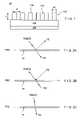
- image 700illustrates a substrate 100 comprising glass, a plurality of regions 150 including alternating first 200 and second 210 index materials, the plurality of regions 150 being positioned substantially adjacent to substrate 100 , and a thin dielectric layer 410 positioned substantially adjacent to the plurality of regions 150 and distal to substrate 100 .
- image 700was taken with a magnification of 91,650 (91K) and shows plurality of regions 150 having a period of approximately 150 nm.
- plurality of regions 150 described hereinaboveillustrates two alternating materials forming a pattern, wherein a first material is designated as “A” and a second material is designated as “B”, such as ABABAB . . .
- other patternsmay also be formed.
- the present inventionmay include other materials within the pattern making up plurality of regions 150 .
- three alternating materialsmay be used creating a pattern such as ABCABCABC . . . .
- four materialsmay be used producing a pattern ABCDABCDABCD . . . .
- Other numbers of materialsmay also be used producing patterns as described herein.
- device 800may include a substrate 100 , an etch stop layer 120 , plurality of regions 150 may include a plurality of filling material 810 , a plurality of high index material 200 , and a plurality of low index material 210 , and anti-reflection coatings 105 and 110 .
- Plurality of regions 150may include a plurality of filling material 810 , a plurality of high index material 200 , and a plurality of low index material 210 arranged in an alternating manner, such as filling material 810 , plurality of low index material 210 , and plurality of high index material 200 , for example.
- filling material 810may have a low or high index.
- Filling material having a low indexmay include SiO 2 , as well as voids of air and vacuum.
- High index material 200may include, as described hereinabove, metals, metal alloys, and combinations of metals. Metals suited for use as the high index material may include aluminum, gold, chromium, by way of non-limiting example only.
- Low index material 210may include SiO 2 , silicon nitride, and silicon, by way of non-limiting example only.
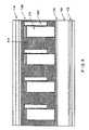
- image 900shows a substrate 100 comprising glass, a plurality of regions 150 including alternating high 200 and low 210 index materials, plurality of filler 810 , an etch stop layer 120 , and anti-reflection coatings 105 and 110 .
- Plurality of regions 150may be positioned substantially adjacent to substrate 100 as shown.
- image 900was taken with a magnification of 72,000 and shows plurality of regions 150 having a period of approximately 200 nm.
Landscapes
- Physics & Mathematics (AREA)
- General Physics & Mathematics (AREA)
- Optics & Photonics (AREA)
- Chemical & Material Sciences (AREA)
- Inorganic Chemistry (AREA)
- Polarising Elements (AREA)
- Surface Treatment Of Optical Elements (AREA)
Abstract
Description
Claims (18)
Priority Applications (1)
| Application Number | Priority Date | Filing Date | Title |
|---|---|---|---|
| US11/832,276US7545564B2 (en) | 2003-02-10 | 2007-08-01 | Universal broadband polarizer, devices incorporating same, and method of making same |
Applications Claiming Priority (4)
| Application Number | Priority Date | Filing Date | Title |
|---|---|---|---|
| US44620003P | 2003-02-10 | 2003-02-10 | |
| US10/644,643US7227684B2 (en) | 2002-08-21 | 2003-08-20 | Method and system for providing beam polarization |
| US10/775,356US7268946B2 (en) | 2003-02-10 | 2004-02-10 | Universal broadband polarizer, devices incorporating same, and method of making same |
| US11/832,276US7545564B2 (en) | 2003-02-10 | 2007-08-01 | Universal broadband polarizer, devices incorporating same, and method of making same |
Related Parent Applications (1)
| Application Number | Title | Priority Date | Filing Date |
|---|---|---|---|
| US10/775,356DivisionUS7268946B2 (en) | 2003-02-10 | 2004-02-10 | Universal broadband polarizer, devices incorporating same, and method of making same |
Publications (2)
| Publication Number | Publication Date |
|---|---|
| US20070297053A1 US20070297053A1 (en) | 2007-12-27 |
| US7545564B2true US7545564B2 (en) | 2009-06-09 |
Family
ID=32871977
Family Applications (2)
| Application Number | Title | Priority Date | Filing Date |
|---|---|---|---|
| US10/775,356Expired - LifetimeUS7268946B2 (en) | 2003-02-10 | 2004-02-10 | Universal broadband polarizer, devices incorporating same, and method of making same |
| US11/832,276Expired - Fee RelatedUS7545564B2 (en) | 2003-02-10 | 2007-08-01 | Universal broadband polarizer, devices incorporating same, and method of making same |
Family Applications Before (1)
| Application Number | Title | Priority Date | Filing Date |
|---|---|---|---|
| US10/775,356Expired - LifetimeUS7268946B2 (en) | 2003-02-10 | 2004-02-10 | Universal broadband polarizer, devices incorporating same, and method of making same |
Country Status (4)
| Country | Link |
|---|---|
| US (2) | US7268946B2 (en) |
| EP (1) | EP1597616A4 (en) |
| JP (1) | JP2006517307A (en) |
| WO (1) | WO2004072692A2 (en) |
Cited By (10)
| Publication number | Priority date | Publication date | Assignee | Title |
|---|---|---|---|---|
| US20110085232A1 (en)* | 2009-10-08 | 2011-04-14 | The Penn State Research Foundation | Multi-spectral filters, mirrors and anti-reflective coatings with subwavelength periodic features for optical devices |
| WO2013156485A1 (en)* | 2012-04-19 | 2013-10-24 | Fraunhofer-Gesellschaft zur Förderung der angewandten Forschung e. V. | Reflective diffraction grating and method for the production thereof |
| US8873144B2 (en) | 2011-05-17 | 2014-10-28 | Moxtek, Inc. | Wire grid polarizer with multiple functionality sections |
| US8913321B2 (en) | 2010-09-21 | 2014-12-16 | Moxtek, Inc. | Fine pitch grid polarizer |
| US8913320B2 (en) | 2011-05-17 | 2014-12-16 | Moxtek, Inc. | Wire grid polarizer with bordered sections |
| US8922890B2 (en) | 2012-03-21 | 2014-12-30 | Moxtek, Inc. | Polarizer edge rib modification |
| US8947772B2 (en) | 2006-08-31 | 2015-02-03 | Moxtek, Inc. | Durable, inorganic, absorptive, ultra-violet, grid polarizer |
| US9348076B2 (en) | 2013-10-24 | 2016-05-24 | Moxtek, Inc. | Polarizer with variable inter-wire distance |
| US9523805B2 (en) | 2010-09-21 | 2016-12-20 | Moxtek, Inc. | Fine pitch wire grid polarizer |
| US10663636B2 (en) | 2017-10-30 | 2020-05-26 | Seiko Epson Corporation | Wire grid polarization apparatus and projection-type display apparatus |
Families Citing this family (109)
| Publication number | Priority date | Publication date | Assignee | Title |
|---|---|---|---|---|
| US8164721B2 (en)* | 2003-12-11 | 2012-04-24 | Tan Kim L | Grating trim retarders |
| US20050275944A1 (en) | 2004-06-11 | 2005-12-15 | Wang Jian J | Optical films and methods of making the same |
| US7670758B2 (en)* | 2004-04-15 | 2010-03-02 | Api Nanofabrication And Research Corporation | Optical films and methods of making the same |
| DE602004019888D1 (en)* | 2004-06-18 | 2009-04-23 | St Microelectronics Res & Dev | Polarization-sensitive solid-state image sensor |
| US20060001969A1 (en)* | 2004-07-02 | 2006-01-05 | Nanoopto Corporation | Gratings, related optical devices and systems, and methods of making such gratings |
| JP4639761B2 (en)* | 2004-11-10 | 2011-02-23 | 旭硝子株式会社 | Polarizer and transmissive liquid crystal projector device |
| US7800823B2 (en) | 2004-12-06 | 2010-09-21 | Moxtek, Inc. | Polarization device to polarize and further control light |
| US7570424B2 (en) | 2004-12-06 | 2009-08-04 | Moxtek, Inc. | Multilayer wire-grid polarizer |
| US7630133B2 (en) | 2004-12-06 | 2009-12-08 | Moxtek, Inc. | Inorganic, dielectric, grid polarizer and non-zero order diffraction grating |
| US7961393B2 (en) | 2004-12-06 | 2011-06-14 | Moxtek, Inc. | Selectively absorptive wire-grid polarizer |
| US7619816B2 (en)* | 2004-12-15 | 2009-11-17 | Api Nanofabrication And Research Corp. | Structures for polarization and beam control |
| US20060127830A1 (en)* | 2004-12-15 | 2006-06-15 | Xuegong Deng | Structures for polarization and beam control |
| JP2006178147A (en)* | 2004-12-22 | 2006-07-06 | Pentax Corp | Sub-wavelength structure optical element with high precision, durability and moisture resistance |
| JP4479535B2 (en)* | 2005-02-21 | 2010-06-09 | セイコーエプソン株式会社 | Optical element manufacturing method |
| KR20070074787A (en)* | 2005-06-13 | 2007-07-18 | 삼성전자주식회사 | Gray voltage generator and liquid crystal display |
| US20070165308A1 (en)* | 2005-12-15 | 2007-07-19 | Jian Wang | Optical retarders and methods of making the same |
| US20070139771A1 (en)* | 2005-12-15 | 2007-06-21 | Jian Wang | Optical retarders and methods of making the same |
| US20070217008A1 (en)* | 2006-03-17 | 2007-09-20 | Wang Jian J | Polarizer films and methods of making the same |
| GB0718706D0 (en) | 2007-09-25 | 2007-11-07 | Creative Physics Ltd | Method and apparatus for reducing laser speckle |
| US20070242352A1 (en)* | 2006-04-13 | 2007-10-18 | Macmaster Steven William | Wire-grid polarizers, methods of fabrication thereof and their use in transmissive displays |
| KR100768241B1 (en)* | 2006-11-10 | 2007-10-17 | 삼성에스디아이 주식회사 | Polarizer and flat panel display including the same |
| JP2010513961A (en)* | 2006-12-22 | 2010-04-30 | シュライフリング ウント アパラーテバウ ゲゼルシャフト ミット ベシュレンクテル ハフツング | Optical rotary coupler with large return loss |
| JP5021357B2 (en)* | 2007-04-16 | 2012-09-05 | 旭化成イーマテリアルズ株式会社 | Thin polarizing plate |
| US7789515B2 (en) | 2007-05-17 | 2010-09-07 | Moxtek, Inc. | Projection device with a folded optical path and wire-grid polarizer |
| JP2008304522A (en)* | 2007-06-05 | 2008-12-18 | Seiko Epson Corp | Polarizing element, manufacturing method of polarizing element, liquid crystal device, and projection display device |
| US8493658B2 (en)* | 2007-07-06 | 2013-07-23 | Semiconductor Energy Laboratory Co., Ltd. | Polarizer and display device including polarizer |
| JP5430126B2 (en)* | 2008-11-13 | 2014-02-26 | キヤノン株式会社 | Polarizer |
| US9335604B2 (en) | 2013-12-11 | 2016-05-10 | Milan Momcilo Popovich | Holographic waveguide display |
| US11726332B2 (en) | 2009-04-27 | 2023-08-15 | Digilens Inc. | Diffractive projection apparatus |
| US8098430B2 (en)* | 2009-05-01 | 2012-01-17 | Toyota Motor Engineering And Manufacturing North America, Inc. | Grating structure for directing non-polarized light |
| US8264773B2 (en)* | 2009-05-01 | 2012-09-11 | Toyota Motor Engineering And Manufacturing North America, Inc. | Grating structure for splitting light |
| US8248696B2 (en) | 2009-06-25 | 2012-08-21 | Moxtek, Inc. | Nano fractal diffuser |
| US8233204B1 (en) | 2009-09-30 | 2012-07-31 | Rockwell Collins, Inc. | Optical displays |
| US10795160B1 (en) | 2014-09-25 | 2020-10-06 | Rockwell Collins, Inc. | Systems for and methods of using fold gratings for dual axis expansion |
| US11300795B1 (en) | 2009-09-30 | 2022-04-12 | Digilens Inc. | Systems for and methods of using fold gratings coordinated with output couplers for dual axis expansion |
| US8675279B2 (en) | 2009-12-15 | 2014-03-18 | Toyota Motor Engineering And Manufacturing North America, Inc. | Grating structure for dividing light |
| US8659826B1 (en) | 2010-02-04 | 2014-02-25 | Rockwell Collins, Inc. | Worn display system and method without requiring real time tracking for boresight precision |
| WO2012108867A1 (en)* | 2011-02-10 | 2012-08-16 | Hewlett-Packard Development Company, L.P. | Grating-based polarizers and optical isolators |
| WO2012136970A1 (en) | 2011-04-07 | 2012-10-11 | Milan Momcilo Popovich | Laser despeckler based on angular diversity |
| WO2016020630A2 (en) | 2014-08-08 | 2016-02-11 | Milan Momcilo Popovich | Waveguide laser illuminator incorporating a despeckler |
| EP2995986B1 (en) | 2011-08-24 | 2017-04-12 | Rockwell Collins, Inc. | Data display |
| US10670876B2 (en) | 2011-08-24 | 2020-06-02 | Digilens Inc. | Waveguide laser illuminator incorporating a despeckler |
| US9715067B1 (en) | 2011-09-30 | 2017-07-25 | Rockwell Collins, Inc. | Ultra-compact HUD utilizing waveguide pupil expander with surface relief gratings in high refractive index materials |
| US9507150B1 (en) | 2011-09-30 | 2016-11-29 | Rockwell Collins, Inc. | Head up display (HUD) using a bent waveguide assembly |
| US9366864B1 (en) | 2011-09-30 | 2016-06-14 | Rockwell Collins, Inc. | System for and method of displaying information without need for a combiner alignment detector |
| US8634139B1 (en) | 2011-09-30 | 2014-01-21 | Rockwell Collins, Inc. | System for and method of catadioptric collimation in a compact head up display (HUD) |
| US20150010265A1 (en) | 2012-01-06 | 2015-01-08 | Milan, Momcilo POPOVICH | Contact image sensor using switchable bragg gratings |
| DE102012101555B4 (en)* | 2012-02-27 | 2013-12-24 | Fraunhofer-Gesellschaft zur Förderung der angewandten Forschung e.V. | Diffraction grating and method for its production |
| JP5938241B2 (en)* | 2012-03-15 | 2016-06-22 | 日立マクセル株式会社 | Optical element and manufacturing method thereof |
| US9523852B1 (en) | 2012-03-28 | 2016-12-20 | Rockwell Collins, Inc. | Micro collimator system and method for a head up display (HUD) |
| CN106125308B (en) | 2012-04-25 | 2019-10-25 | 罗克韦尔柯林斯公司 | Device and method for displaying images |
| US9933684B2 (en) | 2012-11-16 | 2018-04-03 | Rockwell Collins, Inc. | Transparent waveguide display providing upper and lower fields of view having a specific light output aperture configuration |
| US9674413B1 (en) | 2013-04-17 | 2017-06-06 | Rockwell Collins, Inc. | Vision system and method having improved performance and solar mitigation |
| WO2015015138A1 (en) | 2013-07-31 | 2015-02-05 | Milan Momcilo Popovich | Method and apparatus for contact image sensing |
| US10732407B1 (en) | 2014-01-10 | 2020-08-04 | Rockwell Collins, Inc. | Near eye head up display system and method with fixed combiner |
| US9519089B1 (en)* | 2014-01-30 | 2016-12-13 | Rockwell Collins, Inc. | High performance volume phase gratings |
| US9244280B1 (en) | 2014-03-25 | 2016-01-26 | Rockwell Collins, Inc. | Near eye display system and method for display enhancement or redundancy |
| US10359736B2 (en) | 2014-08-08 | 2019-07-23 | Digilens Inc. | Method for holographic mastering and replication |
| WO2016042283A1 (en) | 2014-09-19 | 2016-03-24 | Milan Momcilo Popovich | Method and apparatus for generating input images for holographic waveguide displays |
| US9715110B1 (en) | 2014-09-25 | 2017-07-25 | Rockwell Collins, Inc. | Automotive head up display (HUD) |
| US10088675B1 (en) | 2015-05-18 | 2018-10-02 | Rockwell Collins, Inc. | Turning light pipe for a pupil expansion system and method |
| CN104330847A (en)* | 2014-11-19 | 2015-02-04 | 上海电力学院 | Reflective broadband 1/4 wave plate |
| KR20160060860A (en)* | 2014-11-20 | 2016-05-31 | 삼성디스플레이 주식회사 | Wire grid polarizer, display device including the same and method for fabricating the same |
| WO2016113534A1 (en) | 2015-01-12 | 2016-07-21 | Milan Momcilo Popovich | Environmentally isolated waveguide display |
| US9632226B2 (en) | 2015-02-12 | 2017-04-25 | Digilens Inc. | Waveguide grating device |
| US9618664B2 (en) | 2015-04-15 | 2017-04-11 | Finisar Corporation | Partially etched phase-transforming optical element |
| US10247943B1 (en) | 2015-05-18 | 2019-04-02 | Rockwell Collins, Inc. | Head up display (HUD) using a light pipe |
| US11366316B2 (en) | 2015-05-18 | 2022-06-21 | Rockwell Collins, Inc. | Head up display (HUD) using a light pipe |
| US10126552B2 (en) | 2015-05-18 | 2018-11-13 | Rockwell Collins, Inc. | Micro collimator system and method for a head up display (HUD) |
| US10108010B2 (en) | 2015-06-29 | 2018-10-23 | Rockwell Collins, Inc. | System for and method of integrating head up displays and head down displays |
| WO2017019967A1 (en)* | 2015-07-29 | 2017-02-02 | Sage Electrochromics, Inc. | Laminate including panels and a fill material between the panels and a process of forming the laminate |
| CN113759555B (en) | 2015-10-05 | 2024-09-20 | 迪吉伦斯公司 | Waveguide Display |
| CN105372824B (en) | 2015-12-22 | 2017-12-29 | 苏州苏大维格光电科技股份有限公司 | A kind of bore hole 3D laser display apparatus |
| US10598932B1 (en) | 2016-01-06 | 2020-03-24 | Rockwell Collins, Inc. | Head up display for integrating views of conformally mapped symbols and a fixed image source |
| WO2017131581A1 (en)* | 2016-01-29 | 2017-08-03 | Agency For Science, Technology And Research | Polarization device for polarizing electromagnetic waves, methods of forming and operating the same |
| CN108780224B (en) | 2016-03-24 | 2021-08-03 | 迪吉伦斯公司 | Method and apparatus for providing a polarization selective holographic waveguide device |
| US10890707B2 (en) | 2016-04-11 | 2021-01-12 | Digilens Inc. | Holographic waveguide apparatus for structured light projection |
| US10571614B2 (en) | 2016-08-16 | 2020-02-25 | Moxek, Inc. | Wire grid polarizer heat sink having specified reflective layer, absorptive layer, and heat-dissipation layer |
| US10444410B2 (en) | 2016-08-16 | 2019-10-15 | Moxtek, Inc. | Overcoat wire grid polarizer having conformal coat layer with oxidation barrier and moisture barrier |
| US10408983B2 (en) | 2016-08-16 | 2019-09-10 | Moxtek, Inc. | Durable, high performance wire grid polarizer having permeable junction between top protection layer |
| US10539723B2 (en) | 2016-10-19 | 2020-01-21 | Finisar Corporation | Phase-transforming optical reflector formed by partial etching or by partial etching with reflow |
| US10139537B2 (en) | 2016-11-22 | 2018-11-27 | Moxtek, Inc. | Multiple-stack wire grid polarizer |
| EP3545344A4 (en)* | 2016-11-22 | 2019-11-27 | Moxtek, Inc. | POLARIZER WITH GRID THREAD |
| WO2018102834A2 (en) | 2016-12-02 | 2018-06-07 | Digilens, Inc. | Waveguide device with uniform output illumination |
| US10545346B2 (en) | 2017-01-05 | 2020-01-28 | Digilens Inc. | Wearable heads up displays |
| US10295824B2 (en) | 2017-01-26 | 2019-05-21 | Rockwell Collins, Inc. | Head up display with an angled light pipe |
| US10649121B2 (en)* | 2017-10-05 | 2020-05-12 | Moxtek, Inc. | Low Ts wire grid polarizer |
| WO2019079350A2 (en) | 2017-10-16 | 2019-04-25 | Digilens, Inc. | Systems and methods for multiplying the image resolution of a pixelated display |
| JP7140495B2 (en)* | 2017-12-28 | 2022-09-21 | 株式会社ミツトヨ | Scale and its manufacturing method |
| EP3710876A4 (en) | 2018-01-08 | 2022-02-09 | DigiLens Inc. | SYSTEMS AND METHODS OF FABRICATING WAVEGUIDE CELLS |
| WO2019136476A1 (en) | 2018-01-08 | 2019-07-11 | Digilens, Inc. | Waveguide architectures and related methods of manufacturing |
| EP3710894B1 (en) | 2018-01-08 | 2025-07-30 | Digilens Inc. | Methods for fabricating optical waveguides |
| US10732569B2 (en) | 2018-01-08 | 2020-08-04 | Digilens Inc. | Systems and methods for high-throughput recording of holographic gratings in waveguide cells |
| WO2020023779A1 (en) | 2018-07-25 | 2020-01-30 | Digilens Inc. | Systems and methods for fabricating a multilayer optical structure |
| US20200225471A1 (en) | 2019-01-14 | 2020-07-16 | Digilens Inc. | Holographic Waveguide Display with Light Control Layer |
| JP2022524926A (en)* | 2019-01-31 | 2022-05-11 | キング・アブドゥッラー・ユニバーシティ・オブ・サイエンス・アンド・テクノロジー | Optical processing device based on multi-layer nanodevices |
| US20200247017A1 (en) | 2019-02-05 | 2020-08-06 | Digilens Inc. | Methods for Compensating for Optical Surface Nonuniformity |
| US20220283377A1 (en) | 2019-02-15 | 2022-09-08 | Digilens Inc. | Wide Angle Waveguide Display |
| KR102866596B1 (en) | 2019-02-15 | 2025-09-29 | 디지렌즈 인코포레이티드. | Method and device for providing a holographic waveguide display using an integral grating |
| WO2020186113A1 (en) | 2019-03-12 | 2020-09-17 | Digilens Inc. | Holographic waveguide backlight and related methods of manufacturing |
| JP7296245B2 (en)* | 2019-05-08 | 2023-06-22 | デクセリアルズ株式会社 | Polarizing plate, optical device, and method for producing polarizing plate |
| EP3980825A4 (en) | 2019-06-07 | 2023-05-03 | Digilens Inc. | WAVEGUIDES WITH TRANSMITTING AND REFLECTING GRIDS AND RELATED MANUFACTURING PROCESSES |
| EP4004646A4 (en) | 2019-07-29 | 2023-09-06 | Digilens Inc. | METHODS AND APPARATUS FOR MULTIPLYING THE IMAGE RESOLUTION AND FIELD OF VIEW OF A PIXELATED DISPLAY SCREEN |
| KR102775783B1 (en) | 2019-08-29 | 2025-02-28 | 디지렌즈 인코포레이티드. | Vacuum grid and method for manufacturing the same |
| JP7569164B2 (en)* | 2020-05-12 | 2024-10-17 | デクセリアルズ株式会社 | Polarizing plate, its manufacturing method, and optical device |
| WO2022150841A1 (en) | 2021-01-07 | 2022-07-14 | Digilens Inc. | Grating structures for color waveguides |
| US12158612B2 (en) | 2021-03-05 | 2024-12-03 | Digilens Inc. | Evacuated periodic structures and methods of manufacturing |
| CN113219566B (en)* | 2021-05-10 | 2022-09-16 | 东北师范大学 | Polarization-Sensitive Broadband Responsive Longwave Infrared Metamaterial Absorber |
| US20240393500A1 (en)* | 2023-05-26 | 2024-11-28 | Stmicroelectronics International N.V. | Embedded silicon nanostructures for short-wave-infrared (swir) metaoptics implementation |
Citations (90)
| Publication number | Priority date | Publication date | Assignee | Title |
|---|---|---|---|---|
| JPS61159602A (en) | 1984-12-30 | 1986-07-19 | Olympus Optical Co Ltd | Multi-layered antireflection film |
| US4615034A (en) | 1984-03-30 | 1986-09-30 | Spectra-Physics, Inc. | Ultra-narrow bandwidth optical thin film interference coatings for single wavelength lasers |
| US4638669A (en) | 1985-05-07 | 1987-01-27 | Massachusetts Institute Of Technology | Quantum tunneling cantilever accelerometer |
| US4650289A (en) | 1979-02-21 | 1987-03-17 | Fujitsu Limited | Optical circulator |
| US4732444A (en) | 1985-03-26 | 1988-03-22 | Thomson-Csf | Integrated optics device for optical polarization conversion |
| US4763972A (en) | 1985-09-27 | 1988-08-16 | Thomson-Csf | Differential absorption polarizer, a method of forming same and device implementing said method |
| US4778234A (en) | 1983-06-17 | 1988-10-18 | Thomson Csf | Integrated optics polarizing device |
| US4998793A (en) | 1989-11-14 | 1991-03-12 | At&T Bell Laboratories | Adiabatic polarization manipulating device |
| US5077816A (en) | 1989-12-26 | 1991-12-31 | United Technologies Corporation | Fiber embedded grating frequency standard optical communication devices |
| US5088105A (en) | 1991-03-26 | 1992-02-11 | Spectra Diode Laboratories, Inc. | Optical amplifier with folded light path and laser-amplifier combination |
| US5091981A (en) | 1988-04-29 | 1992-02-25 | Bt&D Technologies Limited | Traveling wave optical modulator |
| US5245471A (en) | 1991-06-14 | 1993-09-14 | Tdk Corporation | Polarizers, polarizer-equipped optical elements, and method of manufacturing the same |
| US5283845A (en) | 1992-07-20 | 1994-02-01 | Jds Fitel Inc. | Multi-port tunable fiber-optic filter |
| US5299212A (en) | 1993-03-10 | 1994-03-29 | At&T Bell Laboratories | Article comprising a wavelength-stabilized semiconductor laser |
| US5461246A (en) | 1994-05-12 | 1995-10-24 | Regents Of The University Of Minnesota | Photodetector with first and second contacts |
| US5467415A (en) | 1994-04-22 | 1995-11-14 | At&T Corp. | Method for making polarization independent silica optical circuits |
| USRE35337E (en) | 1991-07-03 | 1996-09-24 | Bell Communications Research, Inc. | Temperature compensation of liquid-crystal etalon filters |
| US5617234A (en) | 1994-09-26 | 1997-04-01 | Nippon Telegraph & Telephone Corporation | Multiwavelength simultaneous monitoring circuit employing arrayed-waveguide grating |
| US5654818A (en) | 1996-02-09 | 1997-08-05 | The United States Of America As Represented By The United States National Aeronautics And Space Administration | Polarization independent electro-optic modulator |
| US5691989A (en) | 1991-07-26 | 1997-11-25 | Accuwave Corporation | Wavelength stabilized laser sources using feedback from volume holograms |
| US5706301A (en) | 1995-08-16 | 1998-01-06 | Telefonaktiebolaget L M Ericsson | Laser wavelength control system |
| US5719976A (en) | 1995-10-24 | 1998-02-17 | Lucent Technologies, Inc. | Optimized waveguide structure |
| US5726805A (en) | 1996-06-25 | 1998-03-10 | Sandia Corporation | Optical filter including a sub-wavelength periodic structure and method of making |
| US5772905A (en) | 1995-11-15 | 1998-06-30 | Regents Of The University Of Minnesota | Nanoimprint lithography |
| US5777793A (en) | 1996-07-25 | 1998-07-07 | Northern Telecom Limited | Polarization insensitive multilayer planar reflection filters with near ideal spectral response |
| US5793784A (en) | 1997-03-10 | 1998-08-11 | The Research Foundation Of State University Of New York | Apparatus and method for spectral narrowing of high power diode laser arrays |
| US5820769A (en) | 1995-05-24 | 1998-10-13 | Regents Of The University Of Minnesota | Method for making magnetic storage having discrete elements with quantized magnetic moments |
| US5848080A (en) | 1997-05-12 | 1998-12-08 | Dahm; Jonathan S. | Short pulsewidth high pulse repetition frequency laser |
| US5852688A (en) | 1994-09-09 | 1998-12-22 | Gemfire Corporation | Method for manipulating optical energy using poled structure |
| US5870421A (en) | 1997-05-12 | 1999-02-09 | Dahm; Jonathan S. | Short pulsewidth, high pulse repetition frequency laser system |
| US5966483A (en) | 1996-07-02 | 1999-10-12 | Corning Incorporated | Diffraction grating with reduced polarization sensitivity |
| US5973316A (en) | 1997-07-08 | 1999-10-26 | Nec Research Institute, Inc. | Sub-wavelength aperture arrays with enhanced light transmission |
| US5973784A (en) | 1997-01-08 | 1999-10-26 | Electro-Optical Sciences, Inc. | Common path, interferometric systems and methods using a birefringent material for topographic imaging |
| US5991075A (en)* | 1996-11-25 | 1999-11-23 | Ricoh Company, Ltd. | Light polarizer and method of producing the light polarizer |
| US6035089A (en) | 1997-06-11 | 2000-03-07 | Lockheed Martin Energy Research Corporation | Integrated narrowband optical filter based on embedded subwavelength resonant grating structures |
| US6037644A (en) | 1997-09-12 | 2000-03-14 | The Whitaker Corporation | Semi-transparent monitor detector for surface emitting light emitting devices |
| US6040936A (en) | 1998-10-08 | 2000-03-21 | Nec Research Institute, Inc. | Optical transmission control apparatus utilizing metal films perforated with subwavelength-diameter holes |
| US6064506A (en) | 1996-03-05 | 2000-05-16 | Deutsche Telekom Ag | Optical multi-channel separating filter with electrically adjustable photon crystals |
| US6069380A (en) | 1997-07-25 | 2000-05-30 | Regents Of The University Of Minnesota | Single-electron floating-gate MOS memory |
| US6075915A (en) | 1997-03-29 | 2000-06-13 | Koops; Hans W. P. | In-fiber photonic crystals and systems |
| US6101300A (en) | 1997-06-09 | 2000-08-08 | Massachusetts Institute Of Technology | High efficiency channel drop filter with absorption induced on/off switching and modulation |
| US6122103A (en) | 1999-06-22 | 2000-09-19 | Moxtech | Broadband wire grid polarizer for the visible spectrum |
| US6122301A (en) | 1998-06-17 | 2000-09-19 | Santec Corporation | Laser light source apparatus |
| US6125220A (en) | 1998-12-23 | 2000-09-26 | Copner; Nigel | Interferometric optical device including a resonant optical cavity |
| US6127939A (en) | 1996-10-14 | 2000-10-03 | Vehicle Enhancement Systems, Inc. | Systems and methods for monitoring and controlling tractor/trailer vehicle systems |
| US6130969A (en) | 1997-06-09 | 2000-10-10 | Massachusetts Institute Of Technology | High efficiency channel drop filter |
| US6154318A (en) | 1998-08-18 | 2000-11-28 | Coherent, Inc. | Group-delay-dispersive multilayer-mirror structures and method for designing same |
| US6154479A (en) | 1994-10-13 | 2000-11-28 | Nec Corporation | VCSELs (vertical-cavity surface emitting lasers) and VCSEL-based devices |
| US6169825B1 (en) | 1997-08-30 | 2001-01-02 | Bookham Technology Ltd. | Integrated optical polarizer |
| US6175667B1 (en) | 1998-09-22 | 2001-01-16 | Nz Applied Technologies Corporation | High-speed polarization-insensitive electro-optic modulator |
| US6191890B1 (en) | 1996-03-29 | 2001-02-20 | Interuniversitair Micro-Elektronica Centrum Vzw | Optical system with a dielectric subwavelength structure having high reflectivity and polarization selectivity |
| US6198860B1 (en) | 1998-09-22 | 2001-03-06 | Massachusetts Institute Of Technology | Optical waveguide crossings |
| US6198557B1 (en) | 1997-06-25 | 2001-03-06 | Deutsche Telekom Ag | Telecommunication system having frequency-dividing optical components for the parallel processing of optical pulses |
| US6208463B1 (en) | 1998-05-14 | 2001-03-27 | Moxtek | Polarizer apparatus for producing a generally polarized beam of light |
| US6215928B1 (en) | 1996-05-09 | 2001-04-10 | Yeda Research And Development Co. Ltd. | Active wavelength selection with resonant devices |
| US6233375B1 (en) | 1997-04-07 | 2001-05-15 | Schneider Electric Sa | Integrated optics component with polarization effect |
| US6233380B1 (en) | 1998-04-10 | 2001-05-15 | France Telecom | Electrooptic method of signal processing, device for implementing the latter, and use |
| US6235141B1 (en) | 1996-09-27 | 2001-05-22 | Digital Optics Corporation | Method of mass producing and packaging integrated optical subsystems |
| US6240109B1 (en) | 1999-02-25 | 2001-05-29 | Lucent Technologies Inc | Wavelength stabilization of wavelength division multiplexed channels |
| US6253009B1 (en) | 1998-11-24 | 2001-06-26 | Alcatel | Semiconductor optical component comprising a spot-size converter |
| US6252709B1 (en) | 1996-09-30 | 2001-06-26 | Kyocera Corporation | Polarizer and a production method thereof |
| US6251297B1 (en) | 1997-12-22 | 2001-06-26 | Tdk Corporation | Method of manufacturing polarizing plate |
| US6263002B1 (en) | 1997-09-05 | 2001-07-17 | Micron Optics, Inc. | Tunable fiber Fabry-Perot surface-emitting lasers |
| US6262002B1 (en) | 1999-08-11 | 2001-07-17 | Charles C. Carey | Soil remediation compositions and method |
| US6260388B1 (en) | 1998-07-30 | 2001-07-17 | Corning Incorporated | Method of fabricating photonic glass structures by extruding, sintering and drawing |
| US6275291B1 (en) | 1998-09-16 | 2001-08-14 | Nanophotonics Ag | Micropolarimeter and ellipsometer |
| US6285810B1 (en) | 1996-07-26 | 2001-09-04 | Italtel Spa | Tunable add/drop optical device |
| US6288840B1 (en) | 1999-06-22 | 2001-09-11 | Moxtek | Imbedded wire grid polarizer for the visible spectrum |
| US6309580B1 (en) | 1995-11-15 | 2001-10-30 | Regents Of The University Of Minnesota | Release surfaces, particularly for use in nanoimprint lithography |
| US6317554B1 (en) | 1998-08-05 | 2001-11-13 | Nec Corporation | Self-waveguide optical circuit |
| US6324192B1 (en) | 1995-09-29 | 2001-11-27 | Coretek, Inc. | Electrically tunable fabry-perot structure utilizing a deformable multi-layer mirror and method of making the same |
| US6339603B1 (en) | 2000-10-25 | 2002-01-15 | Axsun Technologies, Inc. | Tunable laser with polarization anisotropic amplifier for fabry-perot filter reflection isolation |
| US6349103B1 (en) | 1997-05-07 | 2002-02-19 | Samsung Electronics Co., Ltd. | Cold-start wavelength-division-multiplexed optical transmission system |
| US6353623B1 (en) | 1999-01-04 | 2002-03-05 | Uniphase Telecommunications Products, Inc. | Temperature-corrected wavelength monitoring and control apparatus |
| US6359915B1 (en) | 1999-09-23 | 2002-03-19 | Agere Systems | Wavelength-stabilized Bragg laser |
| US6370177B1 (en) | 1998-03-30 | 2002-04-09 | Kabushiki Kaisha Toshiba | Semiconductor laser and method of manufacturing the same |
| US6374016B2 (en) | 1999-10-20 | 2002-04-16 | Her Majesty The Queen In Right Of Canada, As Represented By The Minister Of Industry | Polarization insensitive grating in a planar channel optical waveguide and method to achieve the same |
| US6371662B1 (en) | 1997-11-26 | 2002-04-16 | Corning Lasertron, Inc. | Spatially variable filter laser wavelength monitoring/control |
| US6400860B1 (en) | 2000-03-21 | 2002-06-04 | Lucent Technologies Inc. | Wavelength selective polarization beam splitter/combiner |
| US6410416B1 (en) | 1999-05-28 | 2002-06-25 | Agere Systems Guardian Corp. | Article comprising a high-resolution pattern on a non-planar surface and method of making the same |
| US6482742B1 (en) | 2000-07-18 | 2002-11-19 | Stephen Y. Chou | Fluid pressure imprint lithography |
| US20020191880A1 (en) | 2001-06-19 | 2002-12-19 | Borrelli Nicholas F. | Method for fabricating an integrated optical isolator and a novel wire grid structure |
| US20030007251A1 (en) | 2000-09-20 | 2003-01-09 | Nobuo Imaizumi | Polarizing function element, optical isolator, laser diode module and method of producing polarizing function element |
| US6518189B1 (en) | 1995-11-15 | 2003-02-11 | Regents Of The University Of Minnesota | Method and apparatus for high density nanostructures |
| US6618104B1 (en) | 1998-07-28 | 2003-09-09 | Nippon Telegraph And Telephone Corporation | Optical device having reverse mode holographic PDLC and front light guide |
| US6661952B2 (en) | 2001-05-04 | 2003-12-09 | Ut Battelle, Llc | Sub-wavelength efficient polarization filter (SWEP filter) |
| US6665119B1 (en)* | 2002-10-15 | 2003-12-16 | Eastman Kodak Company | Wire grid polarizer |
| US6692797B1 (en) | 1999-03-12 | 2004-02-17 | Qinetiq Limited | Photoactive pentaerythritol derivatives and orientation layers |
| US6713238B1 (en) | 1998-10-09 | 2004-03-30 | Stephen Y. Chou | Microscale patterning and articles formed thereby |
| US7113335B2 (en) | 2002-12-30 | 2006-09-26 | Sales Tasso R | Grid polarizer with suppressed reflectivity |
Family Cites Families (11)
| Publication number | Priority date | Publication date | Assignee | Title |
|---|---|---|---|---|
| US4289381A (en)* | 1979-07-02 | 1981-09-15 | Hughes Aircraft Company | High selectivity thin film polarizer |
| FR2572844B1 (en)* | 1984-11-02 | 1986-12-26 | Commissariat Energie Atomique | MAGNETIC MATERIAL OF THE GRENATE TYPE, MAGNETIC FILM WITH HIGH ROTATION FARADAY COMPRISING SUCH A MATERIAL AND METHOD FOR MANUFACTURING THE SAME |
| JPH05289027A (en)* | 1991-06-14 | 1993-11-05 | Tdk Corp | Polarizer, optical element with polarizer and its production |
| JPH06157791A (en)* | 1992-11-25 | 1994-06-07 | Dainippon Printing Co Ltd | Triacetyl cellulose film having scratching resistance, polarizing plate and production thereof |
| JPH06174907A (en)* | 1992-12-04 | 1994-06-24 | Shimadzu Corp | How to make a metal grid |
| JPH0714402U (en)* | 1993-07-30 | 1995-03-10 | 株式会社大真空 | Optical low pass filter |
| JPH10213785A (en)* | 1996-11-25 | 1998-08-11 | Ricoh Co Ltd | Polarizer, method of manufacturing the same, and display or display device including the polarizer |
| JPH10153706A (en)* | 1996-11-25 | 1998-06-09 | Ricoh Co Ltd | Polarizer and method of manufacturing the same |
| US6137939A (en)* | 1997-10-01 | 2000-10-24 | Lucent Technologies Inc. | Method and apparatus for reducing temperature-related spectrum shifts in optical devices |
| JP2001264541A (en)* | 2000-03-21 | 2001-09-26 | Sharp Corp | Hologram element, method of manufacturing the same, and semiconductor laser device using the hologram element |
| US6532111B2 (en)* | 2001-03-05 | 2003-03-11 | Eastman Kodak Company | Wire grid polarizer |
- 2004
- 2004-02-10EPEP04709874Apatent/EP1597616A4/ennot_activeWithdrawn
- 2004-02-10WOPCT/US2004/003892patent/WO2004072692A2/enactiveApplication Filing
- 2004-02-10JPJP2006503459Apatent/JP2006517307A/enactivePending
- 2004-02-10USUS10/775,356patent/US7268946B2/ennot_activeExpired - Lifetime
- 2007
- 2007-08-01USUS11/832,276patent/US7545564B2/ennot_activeExpired - Fee Related
Patent Citations (94)
| Publication number | Priority date | Publication date | Assignee | Title |
|---|---|---|---|---|
| US4650289A (en) | 1979-02-21 | 1987-03-17 | Fujitsu Limited | Optical circulator |
| US4778234A (en) | 1983-06-17 | 1988-10-18 | Thomson Csf | Integrated optics polarizing device |
| US4615034A (en) | 1984-03-30 | 1986-09-30 | Spectra-Physics, Inc. | Ultra-narrow bandwidth optical thin film interference coatings for single wavelength lasers |
| US4615034B1 (en) | 1984-03-30 | 1990-05-29 | Spectra Physics | |
| JPS61159602A (en) | 1984-12-30 | 1986-07-19 | Olympus Optical Co Ltd | Multi-layered antireflection film |
| US4732444A (en) | 1985-03-26 | 1988-03-22 | Thomson-Csf | Integrated optics device for optical polarization conversion |
| US4638669A (en) | 1985-05-07 | 1987-01-27 | Massachusetts Institute Of Technology | Quantum tunneling cantilever accelerometer |
| US4763972A (en) | 1985-09-27 | 1988-08-16 | Thomson-Csf | Differential absorption polarizer, a method of forming same and device implementing said method |
| US5091981A (en) | 1988-04-29 | 1992-02-25 | Bt&D Technologies Limited | Traveling wave optical modulator |
| US4998793A (en) | 1989-11-14 | 1991-03-12 | At&T Bell Laboratories | Adiabatic polarization manipulating device |
| US5077816A (en) | 1989-12-26 | 1991-12-31 | United Technologies Corporation | Fiber embedded grating frequency standard optical communication devices |
| US5088105A (en) | 1991-03-26 | 1992-02-11 | Spectra Diode Laboratories, Inc. | Optical amplifier with folded light path and laser-amplifier combination |
| US5245471A (en) | 1991-06-14 | 1993-09-14 | Tdk Corporation | Polarizers, polarizer-equipped optical elements, and method of manufacturing the same |
| USRE35337E (en) | 1991-07-03 | 1996-09-24 | Bell Communications Research, Inc. | Temperature compensation of liquid-crystal etalon filters |
| US5691989A (en) | 1991-07-26 | 1997-11-25 | Accuwave Corporation | Wavelength stabilized laser sources using feedback from volume holograms |
| US5283845A (en) | 1992-07-20 | 1994-02-01 | Jds Fitel Inc. | Multi-port tunable fiber-optic filter |
| US5299212A (en) | 1993-03-10 | 1994-03-29 | At&T Bell Laboratories | Article comprising a wavelength-stabilized semiconductor laser |
| US5467415A (en) | 1994-04-22 | 1995-11-14 | At&T Corp. | Method for making polarization independent silica optical circuits |
| US5461246A (en) | 1994-05-12 | 1995-10-24 | Regents Of The University Of Minnesota | Photodetector with first and second contacts |
| US5852688A (en) | 1994-09-09 | 1998-12-22 | Gemfire Corporation | Method for manipulating optical energy using poled structure |
| US5617234A (en) | 1994-09-26 | 1997-04-01 | Nippon Telegraph & Telephone Corporation | Multiwavelength simultaneous monitoring circuit employing arrayed-waveguide grating |
| US6154479A (en) | 1994-10-13 | 2000-11-28 | Nec Corporation | VCSELs (vertical-cavity surface emitting lasers) and VCSEL-based devices |
| US5820769A (en) | 1995-05-24 | 1998-10-13 | Regents Of The University Of Minnesota | Method for making magnetic storage having discrete elements with quantized magnetic moments |
| US5956216A (en) | 1995-05-24 | 1999-09-21 | Regents Of The University Of Minnesota | Magnetic storage having discrete elements with quantized magnetic moments |
| US5706301A (en) | 1995-08-16 | 1998-01-06 | Telefonaktiebolaget L M Ericsson | Laser wavelength control system |
| US6324192B1 (en) | 1995-09-29 | 2001-11-27 | Coretek, Inc. | Electrically tunable fabry-perot structure utilizing a deformable multi-layer mirror and method of making the same |
| US5719976A (en) | 1995-10-24 | 1998-02-17 | Lucent Technologies, Inc. | Optimized waveguide structure |
| US6309580B1 (en) | 1995-11-15 | 2001-10-30 | Regents Of The University Of Minnesota | Release surfaces, particularly for use in nanoimprint lithography |
| US5772905A (en) | 1995-11-15 | 1998-06-30 | Regents Of The University Of Minnesota | Nanoimprint lithography |
| US6518189B1 (en) | 1995-11-15 | 2003-02-11 | Regents Of The University Of Minnesota | Method and apparatus for high density nanostructures |
| US5654818A (en) | 1996-02-09 | 1997-08-05 | The United States Of America As Represented By The United States National Aeronautics And Space Administration | Polarization independent electro-optic modulator |
| US6064506A (en) | 1996-03-05 | 2000-05-16 | Deutsche Telekom Ag | Optical multi-channel separating filter with electrically adjustable photon crystals |
| US6191890B1 (en) | 1996-03-29 | 2001-02-20 | Interuniversitair Micro-Elektronica Centrum Vzw | Optical system with a dielectric subwavelength structure having high reflectivity and polarization selectivity |
| US6215928B1 (en) | 1996-05-09 | 2001-04-10 | Yeda Research And Development Co. Ltd. | Active wavelength selection with resonant devices |
| US5726805A (en) | 1996-06-25 | 1998-03-10 | Sandia Corporation | Optical filter including a sub-wavelength periodic structure and method of making |
| US5966483A (en) | 1996-07-02 | 1999-10-12 | Corning Incorporated | Diffraction grating with reduced polarization sensitivity |
| US5777793A (en) | 1996-07-25 | 1998-07-07 | Northern Telecom Limited | Polarization insensitive multilayer planar reflection filters with near ideal spectral response |
| US6285810B1 (en) | 1996-07-26 | 2001-09-04 | Italtel Spa | Tunable add/drop optical device |
| US6235141B1 (en) | 1996-09-27 | 2001-05-22 | Digital Optics Corporation | Method of mass producing and packaging integrated optical subsystems |
| US6252709B1 (en) | 1996-09-30 | 2001-06-26 | Kyocera Corporation | Polarizer and a production method thereof |
| US6127939A (en) | 1996-10-14 | 2000-10-03 | Vehicle Enhancement Systems, Inc. | Systems and methods for monitoring and controlling tractor/trailer vehicle systems |
| US5991075A (en)* | 1996-11-25 | 1999-11-23 | Ricoh Company, Ltd. | Light polarizer and method of producing the light polarizer |
| US5973784A (en) | 1997-01-08 | 1999-10-26 | Electro-Optical Sciences, Inc. | Common path, interferometric systems and methods using a birefringent material for topographic imaging |
| US5793784A (en) | 1997-03-10 | 1998-08-11 | The Research Foundation Of State University Of New York | Apparatus and method for spectral narrowing of high power diode laser arrays |
| US6075915A (en) | 1997-03-29 | 2000-06-13 | Koops; Hans W. P. | In-fiber photonic crystals and systems |
| US6233375B1 (en) | 1997-04-07 | 2001-05-15 | Schneider Electric Sa | Integrated optics component with polarization effect |
| US6349103B1 (en) | 1997-05-07 | 2002-02-19 | Samsung Electronics Co., Ltd. | Cold-start wavelength-division-multiplexed optical transmission system |
| US5848080A (en) | 1997-05-12 | 1998-12-08 | Dahm; Jonathan S. | Short pulsewidth high pulse repetition frequency laser |
| US5870421A (en) | 1997-05-12 | 1999-02-09 | Dahm; Jonathan S. | Short pulsewidth, high pulse repetition frequency laser system |
| US6101300A (en) | 1997-06-09 | 2000-08-08 | Massachusetts Institute Of Technology | High efficiency channel drop filter with absorption induced on/off switching and modulation |
| US6130969A (en) | 1997-06-09 | 2000-10-10 | Massachusetts Institute Of Technology | High efficiency channel drop filter |
| US6035089A (en) | 1997-06-11 | 2000-03-07 | Lockheed Martin Energy Research Corporation | Integrated narrowband optical filter based on embedded subwavelength resonant grating structures |
| US6198557B1 (en) | 1997-06-25 | 2001-03-06 | Deutsche Telekom Ag | Telecommunication system having frequency-dividing optical components for the parallel processing of optical pulses |
| US5973316A (en) | 1997-07-08 | 1999-10-26 | Nec Research Institute, Inc. | Sub-wavelength aperture arrays with enhanced light transmission |
| US6052238A (en) | 1997-07-08 | 2000-04-18 | Nec Research Institute, Inc. | Near-field scanning optical microscope having a sub-wavelength aperture array for enhanced light transmission |
| US6069380A (en) | 1997-07-25 | 2000-05-30 | Regents Of The University Of Minnesota | Single-electron floating-gate MOS memory |
| US6169825B1 (en) | 1997-08-30 | 2001-01-02 | Bookham Technology Ltd. | Integrated optical polarizer |
| US6263002B1 (en) | 1997-09-05 | 2001-07-17 | Micron Optics, Inc. | Tunable fiber Fabry-Perot surface-emitting lasers |
| US6037644A (en) | 1997-09-12 | 2000-03-14 | The Whitaker Corporation | Semi-transparent monitor detector for surface emitting light emitting devices |
| US6371662B1 (en) | 1997-11-26 | 2002-04-16 | Corning Lasertron, Inc. | Spatially variable filter laser wavelength monitoring/control |
| US6251297B1 (en) | 1997-12-22 | 2001-06-26 | Tdk Corporation | Method of manufacturing polarizing plate |
| US6370177B1 (en) | 1998-03-30 | 2002-04-09 | Kabushiki Kaisha Toshiba | Semiconductor laser and method of manufacturing the same |
| US6233380B1 (en) | 1998-04-10 | 2001-05-15 | France Telecom | Electrooptic method of signal processing, device for implementing the latter, and use |
| US6208463B1 (en) | 1998-05-14 | 2001-03-27 | Moxtek | Polarizer apparatus for producing a generally polarized beam of light |
| US6122301A (en) | 1998-06-17 | 2000-09-19 | Santec Corporation | Laser light source apparatus |
| US6618104B1 (en) | 1998-07-28 | 2003-09-09 | Nippon Telegraph And Telephone Corporation | Optical device having reverse mode holographic PDLC and front light guide |
| US6260388B1 (en) | 1998-07-30 | 2001-07-17 | Corning Incorporated | Method of fabricating photonic glass structures by extruding, sintering and drawing |
| US6317554B1 (en) | 1998-08-05 | 2001-11-13 | Nec Corporation | Self-waveguide optical circuit |
| US6154318A (en) | 1998-08-18 | 2000-11-28 | Coherent, Inc. | Group-delay-dispersive multilayer-mirror structures and method for designing same |
| US6275291B1 (en) | 1998-09-16 | 2001-08-14 | Nanophotonics Ag | Micropolarimeter and ellipsometer |
| US6175667B1 (en) | 1998-09-22 | 2001-01-16 | Nz Applied Technologies Corporation | High-speed polarization-insensitive electro-optic modulator |
| US6198860B1 (en) | 1998-09-22 | 2001-03-06 | Massachusetts Institute Of Technology | Optical waveguide crossings |
| US6040936A (en) | 1998-10-08 | 2000-03-21 | Nec Research Institute, Inc. | Optical transmission control apparatus utilizing metal films perforated with subwavelength-diameter holes |
| US6713238B1 (en) | 1998-10-09 | 2004-03-30 | Stephen Y. Chou | Microscale patterning and articles formed thereby |
| US6253009B1 (en) | 1998-11-24 | 2001-06-26 | Alcatel | Semiconductor optical component comprising a spot-size converter |
| US6125220A (en) | 1998-12-23 | 2000-09-26 | Copner; Nigel | Interferometric optical device including a resonant optical cavity |
| US6353623B1 (en) | 1999-01-04 | 2002-03-05 | Uniphase Telecommunications Products, Inc. | Temperature-corrected wavelength monitoring and control apparatus |
| US6240109B1 (en) | 1999-02-25 | 2001-05-29 | Lucent Technologies Inc | Wavelength stabilization of wavelength division multiplexed channels |
| US6692797B1 (en) | 1999-03-12 | 2004-02-17 | Qinetiq Limited | Photoactive pentaerythritol derivatives and orientation layers |
| US6410416B1 (en) | 1999-05-28 | 2002-06-25 | Agere Systems Guardian Corp. | Article comprising a high-resolution pattern on a non-planar surface and method of making the same |
| US6122103A (en) | 1999-06-22 | 2000-09-19 | Moxtech | Broadband wire grid polarizer for the visible spectrum |
| US6288840B1 (en) | 1999-06-22 | 2001-09-11 | Moxtek | Imbedded wire grid polarizer for the visible spectrum |
| US6262002B1 (en) | 1999-08-11 | 2001-07-17 | Charles C. Carey | Soil remediation compositions and method |
| US6359915B1 (en) | 1999-09-23 | 2002-03-19 | Agere Systems | Wavelength-stabilized Bragg laser |
| US6374016B2 (en) | 1999-10-20 | 2002-04-16 | Her Majesty The Queen In Right Of Canada, As Represented By The Minister Of Industry | Polarization insensitive grating in a planar channel optical waveguide and method to achieve the same |
| US6400860B1 (en) | 2000-03-21 | 2002-06-04 | Lucent Technologies Inc. | Wavelength selective polarization beam splitter/combiner |
| US6482742B1 (en) | 2000-07-18 | 2002-11-19 | Stephen Y. Chou | Fluid pressure imprint lithography |
| US20030007251A1 (en) | 2000-09-20 | 2003-01-09 | Nobuo Imaizumi | Polarizing function element, optical isolator, laser diode module and method of producing polarizing function element |
| US6339603B1 (en) | 2000-10-25 | 2002-01-15 | Axsun Technologies, Inc. | Tunable laser with polarization anisotropic amplifier for fabry-perot filter reflection isolation |
| US6661952B2 (en) | 2001-05-04 | 2003-12-09 | Ut Battelle, Llc | Sub-wavelength efficient polarization filter (SWEP filter) |
| US20020191880A1 (en) | 2001-06-19 | 2002-12-19 | Borrelli Nicholas F. | Method for fabricating an integrated optical isolator and a novel wire grid structure |
| US6813077B2 (en) | 2001-06-19 | 2004-11-02 | Corning Incorporated | Method for fabricating an integrated optical isolator and a novel wire grid structure |
| US6665119B1 (en)* | 2002-10-15 | 2003-12-16 | Eastman Kodak Company | Wire grid polarizer |
| US7113335B2 (en) | 2002-12-30 | 2006-09-26 | Sales Tasso R | Grid polarizer with suppressed reflectivity |
Non-Patent Citations (1)
| Title |
|---|
| European Search Report Mar. 5, 2008. |
Cited By (12)
| Publication number | Priority date | Publication date | Assignee | Title |
|---|---|---|---|---|
| US8947772B2 (en) | 2006-08-31 | 2015-02-03 | Moxtek, Inc. | Durable, inorganic, absorptive, ultra-violet, grid polarizer |
| US20110085232A1 (en)* | 2009-10-08 | 2011-04-14 | The Penn State Research Foundation | Multi-spectral filters, mirrors and anti-reflective coatings with subwavelength periodic features for optical devices |
| US8913321B2 (en) | 2010-09-21 | 2014-12-16 | Moxtek, Inc. | Fine pitch grid polarizer |
| US9523805B2 (en) | 2010-09-21 | 2016-12-20 | Moxtek, Inc. | Fine pitch wire grid polarizer |
| US8873144B2 (en) | 2011-05-17 | 2014-10-28 | Moxtek, Inc. | Wire grid polarizer with multiple functionality sections |
| US8913320B2 (en) | 2011-05-17 | 2014-12-16 | Moxtek, Inc. | Wire grid polarizer with bordered sections |
| US8922890B2 (en) | 2012-03-21 | 2014-12-30 | Moxtek, Inc. | Polarizer edge rib modification |
| WO2013156485A1 (en)* | 2012-04-19 | 2013-10-24 | Fraunhofer-Gesellschaft zur Förderung der angewandten Forschung e. V. | Reflective diffraction grating and method for the production thereof |
| US9348076B2 (en) | 2013-10-24 | 2016-05-24 | Moxtek, Inc. | Polarizer with variable inter-wire distance |
| US9354374B2 (en) | 2013-10-24 | 2016-05-31 | Moxtek, Inc. | Polarizer with wire pair over rib |
| US9632223B2 (en) | 2013-10-24 | 2017-04-25 | Moxtek, Inc. | Wire grid polarizer with side region |
| US10663636B2 (en) | 2017-10-30 | 2020-05-26 | Seiko Epson Corporation | Wire grid polarization apparatus and projection-type display apparatus |
Also Published As
| Publication number | Publication date |
|---|---|
| US20040218270A1 (en) | 2004-11-04 |
| EP1597616A2 (en) | 2005-11-23 |
| US7268946B2 (en) | 2007-09-11 |
| WO2004072692A3 (en) | 2005-06-09 |
| EP1597616A4 (en) | 2008-04-09 |
| JP2006517307A (en) | 2006-07-20 |
| US20070297053A1 (en) | 2007-12-27 |
| WO2004072692A2 (en) | 2004-08-26 |
Similar Documents
| Publication | Publication Date | Title |
|---|---|---|
| US7545564B2 (en) | Universal broadband polarizer, devices incorporating same, and method of making same | |
| US7227684B2 (en) | Method and system for providing beam polarization | |
| EP2662711B1 (en) | Method for manufacturing multi-dimensional target waveguide grating and volume grating with micro-structure quasi-phase-matching | |
| US10139538B2 (en) | Wire grid polarizer with high reflectivity on both sides | |
| JP2677353B2 (en) | Optical waveguide | |
| JP5741888B2 (en) | Optical filter and display device | |
| US20110103742A1 (en) | Plasmon waveguide and optical element using the same | |
| Saleki et al. | Broadband terahertz polarizing beam splitter based on a graphene-based defective one-dimensional photonic crystal | |
| US20020122613A1 (en) | Optical device and spectroscopic and integrated optical apparatus using the same | |
| Sabarinathan et al. | Submicron three-dimensional infrared GaAs/Al x O y-based photonic crystal using single-step epitaxial growth | |
| Liu et al. | Highly efficient broadband wave plates using dispersion-engineered high-index-contrast subwavelength gratings | |
| Solli et al. | Photonic crystal based polarization control devices | |
| Soltani et al. | High quality factor polychromatic filters based on hybrid photonic structures | |
| She et al. | High-efficiency polarization beam splitters based on a two-dimensional polymer photoniccrystal | |
| JPH09184937A (en) | Waveguide element | |
| Fang et al. | Optofluidic tunable linear narrow-band filter based on Bragg nanocavity | |
| CN1761892A (en) | Universal broadband polarizer, devices incorporating same, and method of making same | |
| US20090285522A1 (en) | Optical waveguide, optical device, and optical communication device | |
| US11927780B2 (en) | Dielectric grating apparatus | |
| Kawai et al. | Transmittance and time-of-flight study of Al x Ga 1− x As− based photonic crystal waveguides | |
| US20240076231A1 (en) | Fabrication Technique For Wire Grid Polarizer | |
| Bian et al. | Hybrid vanadate silicon nanophotonic platform for extreme light management at telecom bands | |
| JP3764664B2 (en) | Optical circuit | |
| Lemarchand et al. | Interest of hybrid structures for thin-film design: multilayered subwavelength microgratings | |
| CN114265145A (en) | Optical band-pass filter with different polarization bandwidths |
Legal Events
| Date | Code | Title | Description |
|---|---|---|---|
| AS | Assignment | Owner name:NANOOPTO CORPORATION, NEW JERSEY Free format text:ASSIGNMENT OF ASSIGNORS INTEREST;ASSIGNOR:WANG, JIAN JIM;REEL/FRAME:021420/0986 Effective date:20080818 Owner name:NANOOPTO CORPORATION, NEW JERSEY Free format text:ASSIGNMENT OF ASSIGNORS INTEREST;ASSIGNOR:WANG, JIAN JIM;REEL/FRAME:021411/0782 Effective date:20080818 | |
| AS | Assignment | Owner name:API NANOFABRICATION AND RESEARCH CORPORATION, NEW Free format text:ASSIGNMENT OF ASSIGNORS INTEREST;ASSIGNOR:NANOOPTO CORPORATION;REEL/FRAME:021742/0387 Effective date:20070717 | |
| FEPP | Fee payment procedure | Free format text:PAYOR NUMBER ASSIGNED (ORIGINAL EVENT CODE: ASPN); ENTITY STATUS OF PATENT OWNER: LARGE ENTITY | |
| AS | Assignment | Owner name:FISH & RICHARDSON P.C.,MASSACHUSETTS Free format text:LIEN;ASSIGNOR:API NANOFABRICATION AND RESEARCH CORP.;REEL/FRAME:024128/0344 Effective date:20100324 Owner name:FISH & RICHARDSON P.C., MASSACHUSETTS Free format text:LIEN;ASSIGNOR:API NANOFABRICATION AND RESEARCH CORP.;REEL/FRAME:024128/0344 Effective date:20100324 | |
| AS | Assignment | Owner name:ABRAXIS BIOSENSORS, LLC, CALIFORNIA Free format text:ASSIGNMENT OF ASSIGNORS INTEREST;ASSIGNOR:API NANOFABRICATION AND RESEARCH CORPORATION;REEL/FRAME:024964/0001 Effective date:20100611 | |
| AS | Assignment | Owner name:API NANOFABRICATION AND RESEARCH CORP., NEW JERSEY Free format text:RELEASE BY SECURED PARTY;ASSIGNOR:FISH & RICHARDSON P.C.;REEL/FRAME:024964/0677 Effective date:20100910 | |
| FEPP | Fee payment procedure | Free format text:PAYER NUMBER DE-ASSIGNED (ORIGINAL EVENT CODE: RMPN); ENTITY STATUS OF PATENT OWNER: LARGE ENTITY Free format text:PAYOR NUMBER ASSIGNED (ORIGINAL EVENT CODE: ASPN); ENTITY STATUS OF PATENT OWNER: LARGE ENTITY | |
| FEPP | Fee payment procedure | Free format text:PAT HOLDER NO LONGER CLAIMS SMALL ENTITY STATUS, ENTITY STATUS SET TO UNDISCOUNTED (ORIGINAL EVENT CODE: STOL); ENTITY STATUS OF PATENT OWNER: LARGE ENTITY | |
| AS | Assignment | Owner name:NANOOPTO CORPORATION, NEW JERSEY Free format text:NUNC PRO TUNC ASSIGNMENT;ASSIGNOR:WANG, JIAN;REEL/FRAME:028591/0719 Effective date:20070207 | |
| FPAY | Fee payment | Year of fee payment:4 | |
| AS | Assignment | Owner name:NANTOPTICS, LLC, CALIFORNIA Free format text:CHANGE OF NAME;ASSIGNOR:ABRAXIS BIOSENSORS, LLC;REEL/FRAME:030312/0591 Effective date:20120206 | |
| AS | Assignment | Owner name:API TECHNOLOGIES CORP., NEW JERSEY Free format text:ASSIGNMENT OF ASSIGNORS INTEREST;ASSIGNOR:NANTOPTICS LLC;REEL/FRAME:030894/0291 Effective date:20130429 | |
| AS | Assignment | Owner name:BNP PARIBAS, AS COLLATERAL AGENT, NEW YORK Free format text:SECURITY INTEREST;ASSIGNORS:API TECHNOLOGIES CORP.;SPECTRUM CONTROL, INC.;SPECTRUM MICROWAVE, INC.;AND OTHERS;REEL/FRAME:038351/0207 Effective date:20160422 | |
| REMI | Maintenance fee reminder mailed | ||
| LAPS | Lapse for failure to pay maintenance fees | ||
| STCH | Information on status: patent discontinuation | Free format text:PATENT EXPIRED DUE TO NONPAYMENT OF MAINTENANCE FEES UNDER 37 CFR 1.362 | |
| FP | Lapsed due to failure to pay maintenance fee | Effective date:20170609 | |
| AS | Assignment | Owner name:API TECHNOLOGIES CORP., PENNSYLVANIA Free format text:RELEASE BY SECURED PARTY;ASSIGNOR:BNP PARIBAS, AS COLLATERAL AGENT;REEL/FRAME:045604/0054 Effective date:20180420 |