US7542337B2 - Apparatus for reading a multi-level passive element memory cell array - Google Patents
Apparatus for reading a multi-level passive element memory cell arrayDownload PDFInfo
- Publication number
- US7542337B2 US7542337B2US11/461,343US46134306AUS7542337B2US 7542337 B2US7542337 B2US 7542337B2US 46134306 AUS46134306 AUS 46134306AUS 7542337 B2US7542337 B2US 7542337B2
- Authority
- US
- United States
- Prior art keywords
- bit line
- data
- integrated circuit
- read
- reference current
- Prior art date
- Legal status (The legal status is an assumption and is not a legal conclusion. Google has not performed a legal analysis and makes no representation as to the accuracy of the status listed.)
- Active, expires
Links
Images


Classifications
- G—PHYSICS
- G11—INFORMATION STORAGE
- G11C—STATIC STORES
- G11C11/00—Digital stores characterised by the use of particular electric or magnetic storage elements; Storage elements therefor
- G11C11/56—Digital stores characterised by the use of particular electric or magnetic storage elements; Storage elements therefor using storage elements with more than two stable states represented by steps, e.g. of voltage, current, phase, frequency
- G—PHYSICS
- G11—INFORMATION STORAGE
- G11C—STATIC STORES
- G11C13/00—Digital stores characterised by the use of storage elements not covered by groups G11C11/00, G11C23/00, or G11C25/00
- G11C13/0002—Digital stores characterised by the use of storage elements not covered by groups G11C11/00, G11C23/00, or G11C25/00 using resistive RAM [RRAM] elements
- G11C13/0021—Auxiliary circuits
- G11C13/004—Reading or sensing circuits or methods
- G—PHYSICS
- G11—INFORMATION STORAGE
- G11C—STATIC STORES
- G11C13/00—Digital stores characterised by the use of storage elements not covered by groups G11C11/00, G11C23/00, or G11C25/00
- G11C13/0002—Digital stores characterised by the use of storage elements not covered by groups G11C11/00, G11C23/00, or G11C25/00 using resistive RAM [RRAM] elements
- G11C13/0021—Auxiliary circuits
- G11C13/0069—Writing or programming circuits or methods
- G—PHYSICS
- G11—INFORMATION STORAGE
- G11C—STATIC STORES
- G11C13/00—Digital stores characterised by the use of storage elements not covered by groups G11C11/00, G11C23/00, or G11C25/00
- G11C13/0002—Digital stores characterised by the use of storage elements not covered by groups G11C11/00, G11C23/00, or G11C25/00 using resistive RAM [RRAM] elements
- G11C13/0021—Auxiliary circuits
- G11C13/004—Reading or sensing circuits or methods
- G11C2013/0054—Read is performed on a reference element, e.g. cell, and the reference sensed value is used to compare the sensed value of the selected cell
- G—PHYSICS
- G11—INFORMATION STORAGE
- G11C—STATIC STORES
- G11C13/00—Digital stores characterised by the use of storage elements not covered by groups G11C11/00, G11C23/00, or G11C25/00
- G11C13/0002—Digital stores characterised by the use of storage elements not covered by groups G11C11/00, G11C23/00, or G11C25/00 using resistive RAM [RRAM] elements
- G11C13/0021—Auxiliary circuits
- G11C13/0069—Writing or programming circuits or methods
- G11C2013/009—Write using potential difference applied between cell electrodes
- G—PHYSICS
- G11—INFORMATION STORAGE
- G11C—STATIC STORES
- G11C2213/00—Indexing scheme relating to G11C13/00 for features not covered by this group
- G11C2213/70—Resistive array aspects
- G11C2213/77—Array wherein the memory element being directly connected to the bit lines and word lines without any access device being used
Definitions
- the present inventionrelates to semiconductor integrated circuits containing programmable multi-level memory cell arrays, and particularly those arrays incorporating passive element memory cells, and more particularly those having a three-dimensional memory array.
- multi-level memory cellshave been described, particularly three-terminal devices having a charge storage layer such as a floating gate.
- the gate terminal of the memory cellis usually coupled to a word line, and the various memory states are read by application of different voltages on the word line. At each such word line voltage, a current flows on the bit line if the word line voltage is above the programmed threshold voltage, and is sensed.
- Certain passive element memory cellsexhibit re-writable characteristics. For example, in certain memory cells programming may be achieved by forwarding biasing the memory cell (e.g., with reference to the polarity of a diode therewithin) with a voltage of approximately 6-8V, while erase may be achieved by reverse biasing the memory cell with a voltage of approximately 10-14V.
- the LSBmay be mapped as part of one page, and the MSB mapped as part of another page.
- the data statesmay be assigned in a gray scale, in which the highest resistance state (i.e., “un-popped” state) is assigned the 11 state, and the lowest resistance state (i.e., “popped” state) is assigned the 10 state.
- the state assignments for the other two data statesmay be chosen so that the mid-level read reference for the LSB is independent of the MSB.
- the other two data stateshave a resistance between the “popped” 10 state and the “unpopped” 11 state, with the data state closer to the “popped” 10 state being assigned the 00 state, and the data state closer to the “un-popped” 11 state being assigned the 01 state.
- a first reference between the 10 and 00 data states, and a second reference between 01 and 11 data statesmay be used, and the mid-level reference need not be used.
- the inventionis directed to an apparatus for reading a multi-level passive element memory cell array.
- the inventionis defined by the appended claims, and nothing in this section shall be taken as limiting those claims.
- the inventionprovides an integrated circuit which includes: (a) a memory array comprising multi-level passive element memory cells having first, second, third, and fourth memory cell states corresponding respectively to first, second, third, and fourth decreasing resistance levels; and (b) means for discriminating between memory cell states by sensing current on a selected bit line for at least two different combinations of reference current level and read bias voltage on the selected bit line.
- the inventionprovides an integrated circuit which includes: (a) a memory array comprising multi-level passive element memory cells having first, second, third, and fourth memory cell states corresponding respectively to first, second, third, and fourth decreasing resistance levels; (b) a bit line biasing circuit configured to bias a selected bit line with a read bias voltage; (c) a word line biasing circuit configured to bias a selected word line with a selected word line voltage; (d) a sensing circuit configured to generate a first signal and a second signal indicative respectively of a current on the selected bit line relative to a first reference current level and relative to a second reference current level; and (e) a data forming circuit configured to generate a read data value for a first data bit as a function of the first and second signals.
- the inventionprovides an integrated circuit which includes: (a) a memory array comprising multi-level passive element memory cells having first, second, third, and fourth memory cell states corresponding respectively to first, second, third, and fourth decreasing resistance levels; (b) a word line biasing circuit configured to bias a selected word line with a selected word line voltage; (c) a bit line biasing circuit configured to bias, at times, a selected bit line with a first read bias voltage, and to bias, at times, the selected bit line with a second read bias voltage; (d) a sensing circuit configured to generate a first signal indicative of the current on the selected bit line relative to a first reference current level when biased at the first read bias voltage, and to generate a second signal indicative of the current on the selected bit line relative to a second reference current level when biased at the second read bias voltage; and (e) a data forming circuit configured to generate a read data value for a first data bit as a function of the first and second signals.
- the inventionin several aspects is suitable for integrated circuits having a memory array, for methods for operating such integrated circuits and memory arrays, for systems and devices incorporating such integrated circuits and memory arrays, and for computer readable media encodings of such systems, devices, integrated circuits, or memory arrays, all as described herein in greater detail and as set forth in the appended claims.
- the described techniques, structures, and methodsmay be used alone or in combination.
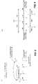
- FIG. 1is a schematic diagram of a memory array, illustrating selected and unselected word lines and bit lines, and depicting row and column circuits coupled thereto.
- FIG. 2is a schematic diagram of the memory array depicted in FIG. 1 , but illustrating exemplary bias conditions in a read mode of operation.
- FIG. 3is a schematic diagram of the memory array depicted in FIG. 1 , illustrating exemplary word line and bit line bias conditions in a forward bias programming mode of operation.
- FIG. 4is a schematic diagram of the memory array depicted in FIG. 1 , illustrating exemplary word line and bit line bias conditions in a reverse bias programming mode of operation.
- FIG. 5is a diagram depicting an exemplary assignment of data states to four resistance levels of a memory cell, and an exemplary order of programming.
- FIG. 6is a diagram depicting an exemplary assignment of data states to four resistance levels of a memory cell, and exemplary sense current levels.
- FIG. 7is an I-V diagram depicting a read condition in accordance with certain embodiments of the present invention.
- FIG. 8is an I-V diagram depicting another read condition in accordance with certain embodiments of the present invention.
- FIG. 9is a schematic/block diagram of a read circuit, including a depiction of the path through a selected memory cell and the word line and bit line selection paths, in accordance with certain embodiments of the present invention.
- FIG. 10is a schematic/block diagram of a write circuit useful for certain embodiments of the present invention.
- FIG. 1is a schematic diagram of an exemplary passive element memory array 100 .
- Two word lines 102 , 104are shown, as well as two bit lines 106 , 108 .
- Word line 102is assumed to be a selected word line (SWL), and word line 104 is assumed to be an unselected word line (UWL).
- bit line 106is assumed to be a selected bit line (SBL), and bit line 108 is assumed to be an unselected bit line (UBL).
- SWLselected word line
- UWLunselected word line
- SBLselected bit line
- UBLunselected bit line
- Four passive element memory cells 101 , 103 , 105 , 107are shown, each coupled between an associated word line and an associated bit line.
- Memory cell 101is associated with the selected word line 102 and the selected bit line 106 , and may be viewed as an “S” cell (i.e., “selected” cell).
- Memory cell 103is associated with the unselected word line 104 and the selected bit line 106 , and may be viewed as an “F” cell (i.e., “off” cell).
- Memory cell 105is associated with the selected word line 102 and the unselected bit line 108 , and may be viewed as an “H” cell (i.e., “halfselected” cell).
- memory cell 107is associated with the unselected word line 104 and the unselected bit line 108 , and may be viewed as a “U” cell (i.e., “unselected” cell).
- the selected and unselected word linesare shown as being generated by a row circuits block 110 , which includes a row decoder circuit.
- the selected and unselected bit linesare shown as being generated by a column and data circuits block 112 , which includes a column decoder circuit and data input/output circuits.
- Both the row circuits 110 and the column and data circuits 112are responsive to address information (i.e., ADDRESS signals) conveyed on bus 114
- the column and data circuits 112are responsive to (and, at times, generate) data signals (i.e., DATA signals) conveyed on I/O bus 116 .
- Such busses 114 , 116may be internal to an integrated circuit, or may represent system busses traversing integrated circuit boundaries and coupled to other integrated circuits.
- Illustrated in FIG. 2are exemplary general biasing conditions for a forward bias mode of operation useful for reading selected memory cell(s). As described elsewhere herein, such a forward bias mode may also be used for a programming mode, a block erase mode, in addition to a read mode (although usually with different voltage levels or conditions for such different modes). As shown, the bias conditions may be viewed as appropriate for a read mode of operation for a selected array block, and will be described as such.
- the selected word line 102is biased at a VSX voltage (e.g., ground), and the selected bit line 106 biased at a VSB voltage (e.g., +2 volts).
- This selected bit line bias voltage VSBmay be viewed as the read voltage VRD, as substantially this entire voltage is impressed across the selected memory cell 101 (since the selected word line is biased at ground), less certain resistive drops in the busses and array lines themselves.
- the unselected word line 104is biased at a VUX voltage equal to the read voltage VRD (e.g., +2 volts), and the unselected bit line 108 is biased at a VUB voltage equal to the selected word line voltage (e.g., ground).
- the S cell 101receives a forward bias voltage equal to VRD (e.g., +2 volts), while the F cell 103 and the H cell 105 receive no bias voltage, and the U cell 107 receives a reverse bias voltage equal to VRD (e.g., ⁇ 2 volts).
- VRDforward bias voltage
- the selected cellwill generate a current on the selected bit line which may be detected, while the F and H cells contribute no current (having no bias thereacross), and the U cells contribute leakage currents between unselected word lines and bit lines.
- exemplary biasing conditionsare depicted for a forward bias programming mode of operation.
- the selected word line 102is biased at a VSX voltage (e.g., ground)
- the selected bit line 106is biased at a VSB voltage (e.g., +8 volts)
- the unselected word line 104is biased at a VUX voltage (e.g., +7.3 volts)
- the unselected bit line 108is biased at a VUB voltage (e.g., +0.7 volts).
- the selected bit line bias voltage VSBnow may be viewed as the programming voltage VPP, as substantially this entire voltage is impressed across the selected memory cell 101 (since the selected word line is biased at ground), less certain resistive drops in the busses and array lines themselves.
- the unselected bit line bias voltage VUBis, preferably set at the apparent “threshold voltage” in a forward biased direction of each memory cell, and is thus shown as a voltage VT being impressed on the unselected bit line 108 .
- the unselected word line bias voltage VUXis also preferably set at a value of VPP ⁇ VT.
- the S cell 101receives a forward bias voltage equal to VPP (e.g., +8 volts)
- the F cell 103receives a forward bias voltage equal to VT (e.g., +0.7 volts)
- the H cell 105receives a forward bias voltage equal to VT (e.g., +0.7 volts)
- the U cell 107receives a reverse bias voltage equal to VPP ⁇ 2VT (e.g., ⁇ 6.6 volts).
- exemplary biasing conditions 200are shown for a reverse bias mode of operation. As described elsewhere herein, such a reverse bias mode may be used for a programming mode or a block erase mode (although usually with different conditions for such different modes). As shown, the bias conditions may be viewed as appropriate for either a programming mode or erase mode of operation for a selected array block, and will be described as such.
- Each of the bias conditions VSX, VUX, VSB, and VUBare now redefined for values appropriate for the present mode of operation.
- the selected word line 102is biased at a VSX voltage of VRR/2 (e.g., +5 volts), and the selected bit line 106 biased at a VSB voltage of ⁇ VRR/2 (e.g., ⁇ 5 volts).
- the unselected word line voltage VUX and the unselected bit line voltage VUBare both ground.
- the S cell 101receives a reverse bias voltage equal in magnitude to VRR (e.g., ⁇ 10 volts)
- the F cell 103receives a reverse bias voltage equal to VRR/2 (e.g., ⁇ 5 volts)
- the H cell 105receives a reverse bias voltage equal to VRR/2 (e.g., ⁇ 5 volts).
- the U cell 107receives no bias across the cell.
- FIG. 5an exemplary assignment of data states is depicted by diagram 180 for an exemplary multi-level passive element memory cell, along with a preferred order of programming such a memory cell to these data states.
- data states 190 , 192 , 194 , and 196represent increasing resistance of the memory cell.
- Data state 196represents an initial “un-popped” state of the memory cell, and has the highest value of resistance of the four data states.
- the initial programming operationchanges the memory cell to a “popped” state, and results in the data state 190 , or the “10” data state.
- Such programming to “pop” the memory cellmay be accomplished using a forward bias programming mode of operation.
- the memory cellmay be further programmed into either of the remaining two data states 192 , 194 , here represented respectively by transitions 186 , 184 , by a reverse bias mode of operation which increases the resistance of the memory cell.
- forward bias and reverse bias programming modesare further described elsewhere herein (including other descriptive material incorporated herein by reference).
- the initial programming operationmay be viewed as programming the LSB, while the second programming operation may be viewed as programming the MSB while preserving the LSB.
- the LSB and MSBare preferably mapped to separate pages of the memory, as described in regards to reading such memory cell described below.
- the LSB datais programmed before the MSB page, and the LSB page is read before determining the programming conditions for the MSB data.
- the MSBmay be determined using two reference levels Ref 1 , Ref 3 .
- the Ref 1 levelis between the 01 and 11 states, and the Ref 3 level is between the 10 and 00 states.
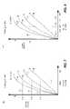
- an I-V (i.e., current-voltage) graph 200represents the current voltage relationship of an exemplary passive element memory cell.
- I-V curves 202 , 204 , 206 , 208are shown, corresponding respectively to data states 190 , 192 , 194 , 196 , and representing respectively data values 10, 00, 01, 11.
- these four statesmay be determined using a single read voltage 210 (VRD) on the selected bit line, by comparing the current generated on the selected bit line against three different reference current levels Iref 1 ( 212 ), Iref 2 ( 214 ), Iref 3 ( 216 ), which correspond respectively to the resistance reference levels Ref 1 , Ref 2 , Ref 3 , described above in reference to FIG. 6 .
- the voltage on the bit lineis set to the VRD voltage, and the bit line current compared to one, two, or three reference current levels. Only one stabilization of the VRD voltage on the SBL is required, yet all four data states may be determined by proper choice of the three reference current levels 212 , 214 , 216 . This method is particularly useful for memory cell currents on the order of 100 nA or more, in which case the magnitude of the Iref 1 current may be approximately 100 nA.
- an I-V graph 220represents another technique.
- the four data statesmay be determined using a single read current 222 on the selected bit line, by comparing the current generated on the selected bit line against a single reference current Iref 1 , for three different read voltage levels Vref 1 ( 228 ), Vref 2 ( 226 ), Vref 3 ( 224 ), which correspond respectively to the resistance reference levels Ref 1 , Ref 2 , Ref 3 , described above.
- the voltage on the bit lineis set to a read voltage VRD equal to one of the three reference voltages 224 , 226 , 228 , and the bit line current compared to the reference current 222 . Only one stabilization of the VRD voltage on the selected bit line is required to determine the LSB, although two stabilizations of the VRD voltage on the selected bit line are required to determine the MSB.
- Vref 1 , Vref 2 , and Vref 3 read voltagesare manipulated so that a single bit line reference current may be used, which allows sense amplifier circuitry to be optimized for such a bias condition.
- This methodmay be particularly useful for memory cells having relatively low currents, such as well below 100 nA for the highest resistance state, because the current level for the high resistance state is set to a higher value than for the technique shown in FIG. 7 by shifting the VRD level to 2.5 volts or even higher.
- Bit line bias circuitry and sense amplifier circuitrymay frequently be more easily optimized when using a higher value of bit line current.
- Another preferred method for setting the referencesis not purely by Iref levels. Since the Icell varies exponentially over the distribution of cells due to the diode current variation, the three Iref levels will traverse a wide range. The sense amplifier may not be as ideally sensitive throughout the wide range of Iref. Therefore this method illustrated by FIG. 8 uses a higher Vref for the lowest reference and a lower Vref for the highest reference. All the comparison operations could use the same Iref value, so the Iref level does not have to change between the first read comparison and the second for faster read speed and less circuit complexity.
- the circuit of FIG. 9is suitable for the technique illustrated by FIG. 8 , where only one current comparison circuit 308 and 309 and OUTA is needed. The OUTB circuitry is not needed.
- the Irefcan be the same for all three reads with the sensitivity of the sense amplifier as ideally designed as possible.
- the read operationis faster because at most two read cycles are required and Iref does not have to change between cycles as described above.
- FIG. 7 and FIG. 8may be combined by varying both the Iref and Vref for the three discrimination levels to produce the largest margin of error in the sensing process.
- FIG. 9depicts an exemplary circuit topology 300 for reading a multi-level memory cell, along with a representation of the word line and bit line selection paths to a selected memory cell 101 .
- This circuitcorresponds generally to the technique described in FIG. 7 .
- a word line selection path 322represents, for example, the path through a word line driver circuit (i.e., a decoder “head”) and to a circuit for generating a decoded source selection bus for the decoder heads, to a ground voltage conveyed on node 324 .
- a bit line selection path 318represents the path through the bit line driver circuit and through any bus coupling circuits to the read circuit.
- An SELB data bus 316represents the input to this read circuit. Additional details of useful decoding circuits are described in the 023-0048 and 023-0054 applications, in the 023-0051 and 023-0056 applications, and in the 023-0053 and 023-0058 applications, all referenced below.
- the desired read voltage VRD on the selected bit lineis provided by way of the clamp device 314 which receives a diode voltage bias signal 315 on its gate.
- Clamp device 314is preferably a native threshold NMOS device.
- This bias signal 315may vary as a function of the location of the selected memory cell along the bit line, and is adjusted to generate a desired read voltage VRD on the selected bit line (i.e., node 106 ).
- a precharge transistor 304is used to precharge various nodes in this topology, including the selected bit line and decoding paths selecting such bit line, in response to an active-low precharge signal XBLP.
- a current mirror device 306provides a current load for the selected bit line.
- the voltage developed on the current mirror gate node 312is coupled to devices 308 , 310 which mirror the bit line current (either with the same magnitude or scaled by the current mirror) to a pair of output stages, each having a respective current source 309 , 311 for providing a high voltage gain output circuit which develops a respective output signal OUTA, OUTB.
- the circuitis powered by a common distributed voltage conveyed on node 302 , which voltage is somewhat higher than the desired read voltage VRD.
- This circuitprovides for setting a desired read voltage on the selected bit line, and further provides for simultaneously comparing the selected bit line current against two different reference currents to generate two different output signals.
- the circuitsimultaneously compares the Icell to multiple Iref currents, as shown by a first current comparator circuit comprising device 308 and current reference 309 and a second current comparator circuit comprising device 310 and current reference 311 .
- OUTA and OUTBare used to determine the memory state as described in more detail above with reference to FIG. 6 .
- These signalsmay be combined by a data forming circuit 326 to generate the MSB.
- a single stabilization time of this voltage on the selected bit lineis sufficient.
- a single one of the OUTA and OUTB outputscan directly generate the LSB (e.g., using a different value of the reference current), with the other output not needed.
- FIG. 10depicts an exemplary circuit topology 350 for writing a multi-level memory cell.
- both the voltage and current of the selected bit lineare cocntrolled to particular values.
- a distributed supply nodeprovides the desired voltage bias (VPP) on bus 352 .
- a diode current bias signal 359 coupled to PMOS transistor 358provides the desired current limit on the selected bit line 106 .
- a precharge device 356functions to precharge the selection path to enhance performance, responsive to an XBLP precharge signal 357 . Both devices 356 , 358 are coupled to node 360 , which is coupled to an SELB bus 316 .
- An analogous circuitsupplies the reverse bias voltage and current to the bit line for the reverse bias (i.e., reset) programming.
- a distributed supply nodeprovides the desired voltage bias ( ⁇ VRR) on bus 361 .
- a diode current bias signal 363 coupled to NMOS transistor 362provides the desired current limit on the selected bit line.
- a precharge device 364functions to precharge the selection path, responsive to a BLP precharge signal 365 . Both devices 362 , 364 are coupled to node 366 which is coupled to an SELN bus 367 .
- Multiple programming operationsmay be used to program the various resistance states as described with reference to FIG. 5 above, and as described in more detail in the MA-163-1 application, referenced below.
- the use of sloped programming pulsesis described in the SAND-01114US0 and SAND-01114US1 applications, referenced below, and techniques for trimming the resistance of multiple cells is described in the SAND-01117US1 applications, referenced below.
- the dual bit line source selection buses SELB and SELNare described in more detail in the 023-0051 and 023-0056 applications, referenced below. Additional insight into useful programming techniques maybe found in U.S. Pat. No. 6,952,030 referenced below.
- Exemplary multi-level memory cellsinclude a passive element cell having a metal oxide (e.g., a transition metal oxide) and a diode.
- Other suitable cellsinclude those having a resistive material in a diode matrix. Examples include a programmable metallization connection, a phase change resistor such as GST material, an organic material variable resistor, a complex metal oxide, a carbon polymer film, a doped chalcogenide glass, and a Schottky barrier diode containing mobile atoms to change resistance.
- the resistive material chosenmay provide one-time-programmable (OTP) memory cells, or write-many memory cells.
- a polysilicon diodecould be employed having conduction modified by reverse bias stress.
- Exemplary multi-level memory cellsare described in the aforementioned U.S. application Ser. No. 11/237,167 and in the MA-163-1 application, referenced below.
- the memory arrayincludes a segmented word line architecture, and preferably a 3D array.
- the word lines on a given word line layerare associated with bit lines on a single bit line layer, while in certain embodiments the word lines on a given word line layer are shared between two bit line layers (i.e., a single word line layer and two bit line layers defining two memory planes) in a so-called “half-mirrored” arrangement.
- bit line layersi.e., a single word line layer and two bit line layers defining two memory planes
- the word line segments for a blockmay be implemented as two inter-digitated groups of word line segments oriented horizontally, and the bit lines for a block may be implemented as two inter-digitated groups of bit lines oriented vertically.
- Each respective group of word lines or bit linesmay be served by a respective decoder/driver circuit and a respective sense circuit on one of the four sides of the array.
- Suitable column and row circuitsincluding hierarchical levels of such decoding, bias circuit organization for the decoded busses, and related supporting circuits, are described in U.S. Pat. No. 6,856,572 by Roy E. Scheuerlein and Matthew P. Crowley, entitled “Multi-Headed Decoder Structure Utilizing Memory Array Line Driver with Dual Purpose Driver Device”; in U.S. Pat. No. 6,859,410 by Roy E. Scheuerlein and Matthew P. Crowley, entitled “Tree Decoder Structure Particularly Well-Suited to Interfacing Array Lines Having Extremely Small Layout Pitch”; in “Dual-Mode Decoder Circuit, Integrated Circuit Memory Array Incorporating Same, and Related Methods of Operation” by Kenneth K.
- Non-mirrored memory arrayse.g., a word line layer associated with only a single bit line layer
- a rowextends across the entire memory bay (if not across the entire stripe) and includes many word lines.
- a bus or line which is “generally spanning the plurality of array blocks”includes spanning almost all the array spanning all but the last block (e.g., a last block to which a given bus is not blocks, such as coupled to).
- “coupling selected bit lines to a first bus”means respectively coupling each such selected bit line to a corresponding bus line of the first bus.
- word lines (e.g., including word line segments) and bit linesusually represent orthogonal array lines, and generally follow a common assumption in the art that word lines are driven and bit lines are sensed, at least during a read operation.
- a “global line”(e.g., a global select line) is an array line that spans more than one memory block, but no particular inference should be drawn suggesting such a global line must traverse across an entire memory array or substantially across an entire integrated circuit.
- sensing a current relative to a reference currentis taken to mean determining if the “sensed” current is greater or less than the reference current.
- a passive element memory arrayincludes a plurality of 2-terminal memory cells, each connected between an associated X-line (e.g., word line) and an associated Y-line (e.g., bit line).
- Such a memory arraymay be a two-dimensional (planar) array or may be a three-dimensional array having more than one plane of memory cells.
- Each such memory cellhas a non-linear conductivity in which the current in a reverse direction (i.e., from cathode to anode) is lower than the current in a forward direction.
- a passive element memory arraymay be a one-time programmable (i.e., write once) memory array or a read/write (i.e., write many) memory array.
- Such passive element memory cellsmay generally be viewed as having a current steering element directing current in a direction and another component which is capable of changing its state (e.g., a fuse, an antifuse, a capacitor, a resistive element, etc.).
- the programming state of the memory elementcan be read by sensing current flow or voltage drop when the memory element is selected.
- an integrated circuit memory arrayis a monolithic integrated circuit structure, rather than more than one integrated circuit device packaged together or in close proximity.
- nodemay actually represent a pair of nodes for conveying a differential signal, or may represent multiple separate wires (e.g., a bus) for carrying several related signals or for carrying a plurality of signals forming a digital word or other multi-bit signal.
- circuits and physical structuresare generally presumed, it is well recognized that in modern semiconductor design and fabrication, physical structures and circuits may be embodied in computer readable descriptive form suitable for use in subsequent design, test or fabrication stages as well as in resultant fabricated semiconductor integrated circuits. Accordingly, claims directed to traditional circuits or structures may, consistent with particular language thereof, read upon computer readable encodings and representations of same, whether embodied in media or combined with suitable reader facilities to allow fabrication, test, or design refinement of the corresponding circuits and/or structures.
- the inventionis contemplated to include circuits, related methods or operation, related methods for making such circuits, and computer-readable medium encodings of such circuits and methods, all as described herein, and as defined in the appended claims.
- a computer-readable mediumincludes at least disk, tape, or other magnetic, optical, semiconductor (e.g., flash memory cards, ROM), or electronic medium and a network, wireline, wireless or other communications medium.
- An encoding of a circuitmay include circuit schematic information, physical layout information, behavioral simulation information, and/or may include any other encoding from which the circuit may be represented or communicated.
Landscapes
- Engineering & Computer Science (AREA)
- Computer Hardware Design (AREA)
- Semiconductor Memories (AREA)
- Read Only Memory (AREA)
Abstract
Description
- U.S. Pat. No. 6,034,882 entitled “Vertically Stacked Field Programmable Nonvolatile Memory and Method of Fabrication” to Mark G. Johnson, et al.;
- U.S. Pat. No. 6,420,215 entitled “Three Dimensional Memory Array and Method of Fabrication” to N. Johan Knall, et al.;
- U.S. Pat. No. 6,525,953 entitled “Vertically-Stacked, Field Programmable, Nonvolatile Memory and Method of Fabrication” to Mark Johnson, et al.;
- U.S. Pat. No. 6,490,218 entitled “Digital Memory Method and System for Storing Multiple-Bit Digital Data” to Michael Vyvoda, et al.;
- U.S. Pat. No. 6,952,043 entitled “Electrically Isolated Pillars in Active Devices” to Michael Vyvoda, et al.; and
- U.S. Patent Application Publication No. US2005-0052915 entitled “Nonvolatile Memory Cell Without a Dielectric Antifuse Having High- and Low-Impedance States” by S. Brad Herner, et al.
- U.S. application Ser. No. 11/496,985, now U.S. Publication No. 2007/0069276, entitled “Multi-Use Memory Cell and Memory Array” by Roy Scheuerlein and Tanmay Kumar (the“10519-141” application);
- U.S. application Ser. No. 11/496,984, now U.S. Publication No. 2007/0070690, entitled“Method for Using a Multi-Use Memory Cell and Memory Array” by Roy Scheuerlein and Tanmay Kumar (the “10519-150” application);
- U.S. application Ser. No. 11/496,874, now U.S. Publication No. 2008-0023790, entitled“Mixed-Use Memory Array” by Roy Scheuerlein (the “10519-142” application);
- U.S. application Ser. No. 11/496,983, now U.S. Publication No. 2008-0025118, entitled“Method for Using a Mixed-Use Memory Array” by Roy Scheuerlein (the “10519-151” application);
- U.S. application Ser. No. 11/496,870, now U.S. Publication No. 2008-0025069, entitled “Mixed-Use Memory Array With Different Data States” by Roy Scheuerlein and Christopher Petti (the “10519-149” application);
- U.S. application Ser. No. 11/497,021, now U.S. Publication No. 2008-0025062, entitled “Method for Using a Mixed-Use Memory Array With Different Data States” by Roy Scheuerlein and Christopher Petti (the “10519-152” application);
- U.S. application Ser. No. 11/461,393, now U.S. Publication No. 2008-0025076, entitled “Controlled Pulse Operations in Non-Volatile Memory” by Roy Scheuerlein (the “SAND-01114US0” application);
- U.S. application Ser. No. 11/461,399, now U.S. Publication No. 2008-0025077, entitled “Systems for Controlled Pulse Operations in Non-Volatile Memory” by Roy Scheuerlein (the “SAND-01114US1” application);
- U.S. application Ser. No. 11/461,410, now U.S. Publication No. 2008-0025061, entitled “High Bandwidth One-Time Field-Programmable Memory” by Roy Scheuerlein and Christopher J. Petti (the “SAND-01115US0” application);
- U.S. application Ser. No. 11/461,419, now U.S. Publication No. 2008-0025067, entitled “Systems for High Bandwidth One-Time Field-Programmable Memory” by Roy Scheuerlein and Christopher J. Petti (the “SAND-0115US1” application);
- U.S. application Ser. No. 11/461,424, now U.S. Publication No. 2008-0025068, entitled “Reverse Bias Trim Operations in Non-Volatile Memory” by Roy Scheuerlein and Tanmay Kumar (the “SAND-01117US0” application);
- U.S. application Ser. No. 11/461,431, now U.S. Publication No. 2008-0025078, entitled “Systems for Reverse Bias Trim Operations in Non-Volatile Memory” by Roy Scheuerlein and Tanmay Kumar (the “SAND-01117US1” application);
- U.S. application Ser. No. 11/496,986, now U.S. Publication No. 2007-0072360, entitled “Method for Using a Memory Cell Comprising Switchable Semiconductor Memory Element with Trimmable Resistance” by Tanmay Kumar, S. Brad Herner, Roy E. Scheuerlein, and Christopher J. Petti (the “MA-163-1” application);
- U.S. application Ser. No. 11/461,339, now U.S. Publication No. 2008-0025066, entitled “Passive Element Memory Array Incorporating Reversible Polarity Word Line and Bit Line Decoders” by Luca G. Fasoli, Christopher J. Petti, and Roy E. Scheuerlein (the “023-0048” application);
- U.S. application Ser. No. 11/461,364, now U.S. Publication No. 2008-0025132, entitled “Method for Using a Passive Element Memory Array Incorporating Reversible Polarity Word Line and Bit Line Decoders” by Luca G. Fasoli, Christopher J. Petti, and Roy E. Scheuerlein (the “023-0054” application);
- U.S. application Ser. No. 11/461,343, now U.S. Publication No. 2008-0025088, entitled “Apparatus for Reading a Multi-Level Passive Element Memory Cell Array” by Roy E. Scheuerlein, Tyler Thorp, and Luca G. Fasoli (the “023-0049” application);
- U.S. application Ser. No. 11/461,367, now U.S. Publication No. 2008-0025089, entitled “Method for Reading a Multi-Level Passive Element Memory Cell Array” by Roy E. Scheuerlein, Tyler Thorp, and Luca G. Fasoli (the “023-0055” application);
- U.S. application Ser. No. 11/461,352, now U.S. Publication No. 2008-0025131, entitled “Dual Data-Dependent Busses for Coupling Read/Write Circuits to a Memory Array” by Roy E. Scheuerlein and Luca G. Fasoli (the “023-0051” application);
- U.S. application Ser. No. 11/461,369, now U.S. Publication No. 2008-0025133, entitled “Method for Using Dual Data-Dependent Busses for Coupling Read/Write Circuits to a Memory Array” by Roy E. Scheuerlein and Luca G. Fasoli (the “023-0056” application);
- U.S. application Ser. No. 11/461,359, now U.S. Publication No. 2008-0025085entitled “Memory Array Incorporating Two Data Busses for Memory Array Block Selection” by Roy E. Scheuerlein, Luca G. Fasoli, and Christopher J. Petti (the “023-0052” application);
- U.S. application Ser. No. 11/461,372, now U.S. Publication No. 2008-0025134, entitled “Method for Using Two Data Busses for Memory Array Block Selection” by Roy E. Scheuerlein, Luca G. Fasoli, and Christopher J. Petti (the “023-0057” application);
- U.S. application Ser. No. 11/461,362, now U.S. Publication No. 2008-0025093, entitled“Hierarchical Bit Line Bias Bus for Block Selectable Memory Array” by Roy E. Scheuerlein and Luca G. Fasoli (the “023-0053” application); and
- U.S. application Ser. No. 11/461,376, now U.S. Publication No. 2008-0025094, entitled “Method for Using a Hierarchical Bit Line Bias Bus for Block Selectable Memory Array” by Roy E. Scheuerlein and Luca G. Fasoli (the “023-0058” application).
Claims (27)
Priority Applications (7)
| Application Number | Priority Date | Filing Date | Title |
|---|---|---|---|
| US11/461,343US7542337B2 (en) | 2006-07-31 | 2006-07-31 | Apparatus for reading a multi-level passive element memory cell array |
| CN2007800330616ACN101512663B (en) | 2006-07-31 | 2007-07-31 | Method and apparatus for reading multi-level passive element memory cell array |
| KR1020097004237AKR101446581B1 (en) | 2006-07-31 | 2007-07-31 | Method and apparatus for reading a multi-level passive element memory cell array |
| PCT/US2007/074899WO2008016946A2 (en) | 2006-07-31 | 2007-07-31 | Method and apparatus for reading a multi-level passive element memory cell array |
| TW096128067ATWI378551B (en) | 2006-07-31 | 2007-07-31 | Method and apparatus for reading a multi-level passive element memory cell array |
| EP07799950.6AEP2052390B1 (en) | 2006-07-31 | 2007-07-31 | Method and apparatus for reading a multi-level passive element memory cell array |
| JP2009523027AJP5207081B2 (en) | 2006-07-31 | 2007-07-31 | Method and apparatus for reading a multilevel passive element memory cell array |
Applications Claiming Priority (1)
| Application Number | Priority Date | Filing Date | Title |
|---|---|---|---|
| US11/461,343US7542337B2 (en) | 2006-07-31 | 2006-07-31 | Apparatus for reading a multi-level passive element memory cell array |
Publications (2)
| Publication Number | Publication Date |
|---|---|
| US20080025088A1 US20080025088A1 (en) | 2008-01-31 |
| US7542337B2true US7542337B2 (en) | 2009-06-02 |
Family
ID=38986076
Family Applications (1)
| Application Number | Title | Priority Date | Filing Date |
|---|---|---|---|
| US11/461,343Active2027-04-19US7542337B2 (en) | 2006-07-31 | 2006-07-31 | Apparatus for reading a multi-level passive element memory cell array |
Country Status (2)
| Country | Link |
|---|---|
| US (1) | US7542337B2 (en) |
| CN (1) | CN101512663B (en) |
Cited By (6)
| Publication number | Priority date | Publication date | Assignee | Title |
|---|---|---|---|---|
| US20130070512A1 (en)* | 2011-09-19 | 2013-03-21 | Hyuck-Sang Yim | Non-volatile memory device |
| US20150294696A1 (en)* | 2014-04-10 | 2015-10-15 | Taiwan Semiconductor Manufacturing Company Limited | Stabilizing circuit |
| US9779806B2 (en) | 2011-02-25 | 2017-10-03 | Micron Technology, Inc. | Resistive memory sensing methods and devices |
| USRE46623E1 (en)* | 2009-06-19 | 2017-12-05 | Samsung Electronics Co., Ltd. | Programming methods for three-dimensional memory devices having multi-bit programming, and three-dimensional memory devices programmed thereby |
| US9881671B2 (en) | 2015-02-17 | 2018-01-30 | Samsung Electronics Co., Ltd. | Resistive memory device, resistive memory system, and method of operating the resistive memory system |
| USRE46994E1 (en)* | 2007-06-12 | 2018-08-14 | Samsung Electronics Co., Ltd. | Flash memory devices having three dimensional stack structures and methods of driving same |
Families Citing this family (17)
| Publication number | Priority date | Publication date | Assignee | Title |
|---|---|---|---|---|
| US7492630B2 (en)* | 2006-07-31 | 2009-02-17 | Sandisk 3D Llc | Systems for reverse bias trim operations in non-volatile memory |
| US7522448B2 (en)* | 2006-07-31 | 2009-04-21 | Sandisk 3D Llc | Controlled pulse operations in non-volatile memory |
| US7542338B2 (en) | 2006-07-31 | 2009-06-02 | Sandisk 3D Llc | Method for reading a multi-level passive element memory cell array |
| US7499355B2 (en)* | 2006-07-31 | 2009-03-03 | Sandisk 3D Llc | High bandwidth one time field-programmable memory |
| US7499366B2 (en) | 2006-07-31 | 2009-03-03 | Sandisk 3D Llc | Method for using dual data-dependent busses for coupling read/write circuits to a memory array |
| US7719874B2 (en)* | 2006-07-31 | 2010-05-18 | Sandisk 3D Llc | Systems for controlled pulse operations in non-volatile memory |
| US8279704B2 (en) | 2006-07-31 | 2012-10-02 | Sandisk 3D Llc | Decoder circuitry providing forward and reverse modes of memory array operation and method for biasing same |
| US7499304B2 (en)* | 2006-07-31 | 2009-03-03 | Sandisk 3D Llc | Systems for high bandwidth one time field-programmable memory |
| US7495947B2 (en)* | 2006-07-31 | 2009-02-24 | Sandisk 3D Llc | Reverse bias trim operations in non-volatile memory |
| US7961494B2 (en) | 2008-04-11 | 2011-06-14 | Sandisk 3D Llc | Non-volatile multi-level re-writable memory cell incorporating a diode in series with multiple resistors and method for writing same |
| EP2182544A1 (en)* | 2008-10-31 | 2010-05-05 | FEI Company | Charged-particle optical system with dual specimen loading options |
| JP2011204302A (en)* | 2010-03-24 | 2011-10-13 | Toshiba Corp | Semiconductor memory device |
| WO2013015768A1 (en)* | 2011-07-22 | 2013-01-31 | Hewlett-Packard Development Company, L.P. | Circuit and method for reading a resistive switching device in an array |
| CN105103235B (en)* | 2013-01-31 | 2020-03-10 | 慧与发展有限责任合伙企业 | Non-volatile multi-level cell memory with decoupled bits for higher performance and energy efficiency |
| KR20140128482A (en)* | 2013-04-25 | 2014-11-06 | 에스케이하이닉스 주식회사 | Resistance Memory Device and Write Control Circuit, Memory Apparatus and Data Processing System Having the Same, and Operation Method Therefor |
| US10360973B2 (en)* | 2016-12-23 | 2019-07-23 | Western Digital Technologies, Inc. | Data mapping enabling fast read multi-level 3D NAND to improve lifetime capacity |
| KR102671481B1 (en)* | 2019-07-19 | 2024-06-03 | 삼성전자주식회사 | Memory device for avoiding multi-turn on of memory cell, and operating method thereof |
Citations (61)
| Publication number | Priority date | Publication date | Assignee | Title |
|---|---|---|---|---|
| US2632058A (en)* | 1946-03-22 | 1953-03-17 | Bell Telephone Labor Inc | Pulse code communication |
| US3761896A (en) | 1972-04-18 | 1973-09-25 | Ibm | Memory array of cells containing bistable switchable resistors |
| US5541869A (en) | 1991-10-22 | 1996-07-30 | British Telecommunications, Plc | Resistive memory element |
| US5666304A (en) | 1994-02-10 | 1997-09-09 | Mega Chips Corporation | Semiconductor memory device and method of fabricating the same |
| US5915167A (en) | 1997-04-04 | 1999-06-22 | Elm Technology Corporation | Three dimensional structure memory |
| US6034882A (en) | 1998-11-16 | 2000-03-07 | Matrix Semiconductor, Inc. | Vertically stacked field programmable nonvolatile memory and method of fabrication |
| US6072716A (en) | 1999-04-14 | 2000-06-06 | Massachusetts Institute Of Technology | Memory structures and methods of making same |
| US6385074B1 (en) | 1998-11-16 | 2002-05-07 | Matrix Semiconductor, Inc. | Integrated circuit structure including three-dimensional memory array |
| US6420215B1 (en) | 2000-04-28 | 2002-07-16 | Matrix Semiconductor, Inc. | Three-dimensional memory array and method of fabrication |
| US6473332B1 (en) | 2001-04-04 | 2002-10-29 | The University Of Houston System | Electrically variable multi-state resistance computing |
| US6490218B1 (en) | 2001-08-17 | 2002-12-03 | Matrix Semiconductor, Inc. | Digital memory method and system for storing multiple bit digital data |
| US20030021148A1 (en) | 2001-03-21 | 2003-01-30 | Scheuerlein Roy E. | Current sensing method and apparatus particularly useful for a memory array of cells having diode-like characteristics |
| US6525953B1 (en) | 2001-08-13 | 2003-02-25 | Matrix Semiconductor, Inc. | Vertically-stacked, field-programmable, nonvolatile memory and method of fabrication |
| US20030047765A1 (en) | 2001-08-30 | 2003-03-13 | Campbell Kristy A. | Stoichiometry for chalcogenide glasses useful for memory devices and method of formation |
| US20030053332A1 (en)* | 2000-04-28 | 2003-03-20 | Bendik Kleveland | Three-dimensional memory array incorporating serial chain diode stack |
| US6545898B1 (en) | 2001-03-21 | 2003-04-08 | Silicon Valley Bank | Method and apparatus for writing memory arrays using external source of high programming voltage |
| US6618295B2 (en) | 2001-03-21 | 2003-09-09 | Matrix Semiconductor, Inc. | Method and apparatus for biasing selected and unselected array lines when writing a memory array |
| US6711068B2 (en) | 2002-06-28 | 2004-03-23 | Motorola, Inc. | Balanced load memory and method of operation |
| US6735104B2 (en) | 2001-03-21 | 2004-05-11 | Matrix Semiconductor, Inc. | Memory device with row and column decoder circuits arranged in a checkerboard pattern under a plurality of memory arrays |
| US6753561B1 (en) | 2002-08-02 | 2004-06-22 | Unity Semiconductor Corporation | Cross point memory array using multiple thin films |
| US6795340B2 (en) | 2002-01-10 | 2004-09-21 | Nec Corporation | Non-volatile magnetic memory |
| US6801448B2 (en) | 2002-11-26 | 2004-10-05 | Sharp Laboratories Of America, Inc. | Common bit/common source line high density 1T1R R-RAM array |
| US6831854B2 (en) | 2002-08-02 | 2004-12-14 | Unity Semiconductor Corporation | Cross point memory array using distinct voltages |
| US6834008B2 (en) | 2002-08-02 | 2004-12-21 | Unity Semiconductor Corporation | Cross point memory array using multiple modes of operation |
| US6841833B2 (en) | 2002-09-26 | 2005-01-11 | Sharp Laboratories Of America, Inc. | 1T1R resistive memory |
| US6850429B2 (en) | 2002-08-02 | 2005-02-01 | Unity Semiconductor Corporation | Cross point memory array with memory plugs exhibiting a characteristic hysteresis |
| US6856572B2 (en) | 2000-04-28 | 2005-02-15 | Matrix Semiconductor, Inc. | Multi-headed decoder structure utilizing memory array line driver with dual purpose driver device |
| US6856536B2 (en) | 2002-08-02 | 2005-02-15 | Unity Semiconductor Corporation | Non-volatile memory with a single transistor and resistive memory element |
| US6859382B2 (en) | 2002-08-02 | 2005-02-22 | Unity Semiconductor Corporation | Memory array of a non-volatile ram |
| US6859410B2 (en) | 2002-11-27 | 2005-02-22 | Matrix Semiconductor, Inc. | Tree decoder structure particularly well-suited to interfacing array lines having extremely small layout pitch |
| US6879505B2 (en) | 2003-03-31 | 2005-04-12 | Matrix Semiconductor, Inc. | Word line arrangement having multi-layer word line segments for three-dimensional memory array |
| US6881623B2 (en) | 2001-08-29 | 2005-04-19 | Micron Technology, Inc. | Method of forming chalcogenide comprising devices, method of forming a programmable memory cell of memory circuitry, and a chalcogenide comprising device |
| US6906939B2 (en) | 2002-08-02 | 2005-06-14 | Unity Semiconductor Corporation | Re-writable memory with multiple memory layers |
| US6917539B2 (en) | 2002-08-02 | 2005-07-12 | Unity Semiconductor Corporation | High-density NVRAM |
| US6927411B2 (en) | 2000-02-11 | 2005-08-09 | Axon Technologies Corporation | Programmable structure, an array including the structure, and methods of forming the same |
| US20050201148A1 (en) | 2004-03-12 | 2005-09-15 | Super Talent Electronics, Inc. | Flash memory device and architecture with multi level cells |
| US6952030B2 (en) | 2002-12-19 | 2005-10-04 | Matrix Semiconductor, Inc. | High-density three-dimensional memory cell |
| US6965137B2 (en) | 2002-08-02 | 2005-11-15 | Unity Semiconductor Corporation | Multi-layer conductive memory device |
| US20050276091A1 (en)* | 2004-06-15 | 2005-12-15 | Sharp Kabushiki Kaisha | Semiconductor memory device |
| US7038935B2 (en) | 2002-08-02 | 2006-05-02 | Unity Semiconductor Corporation | 2-terminal trapped charge memory device with voltage switchable multi-level resistance |
| US7057922B2 (en) | 2003-09-12 | 2006-06-06 | Sharp Kabushiki Kaisha | Nonvolatile semiconductor memory device |
| US20060146639A1 (en) | 2004-12-30 | 2006-07-06 | Matrix Semiconductor, Inc. | Apparatus and method for hierarchical decoding of dense memory arrays using multiple levels of multiple-headed decoders |
| US20060250836A1 (en) | 2005-05-09 | 2006-11-09 | Matrix Semiconductor, Inc. | Rewriteable memory cell comprising a diode and a resistance-switching material |
| US20060250837A1 (en) | 2005-05-09 | 2006-11-09 | Sandisk 3D, Llc | Nonvolatile memory cell comprising a diode and a resistance-switching material |
| US7142471B2 (en) | 2005-03-31 | 2006-11-28 | Sandisk 3D Llc | Method and apparatus for incorporating block redundancy in a memory array |
| US20060273298A1 (en) | 2005-06-02 | 2006-12-07 | Matrix Semiconductor, Inc. | Rewriteable memory cell comprising a transistor and resistance-switching material in series |
| US20070007579A1 (en) | 2005-07-11 | 2007-01-11 | Matrix Semiconductor, Inc. | Memory cell comprising a thin film three-terminal switching device having a metal source and /or drain region |
| US20070008773A1 (en) | 2005-07-11 | 2007-01-11 | Matrix Semiconductor, Inc. | Nonvolatile memory cell comprising switchable resistor and transistor |
| US20070008786A1 (en) | 2005-07-11 | 2007-01-11 | Scheuerlein Roy E | Apparatus and method for reading an array of nonvolatile memory cells including switchable resistor memory elements |
| US20070008785A1 (en) | 2005-07-11 | 2007-01-11 | Scheuerlein Roy E | Apparatus and method for programming an array of nonvolatile memory cells including switchable resistor memory elements |
| US20070069276A1 (en) | 2005-09-28 | 2007-03-29 | Scheuerlein Roy E | Multi-use memory cell and memory array |
| US20070072360A1 (en) | 2005-09-28 | 2007-03-29 | Tanmay Kumar | Method for using a memory cell comprising switchable semiconductor memory element with trimmable resistance |
| US7233024B2 (en) | 2003-03-31 | 2007-06-19 | Sandisk 3D Llc | Three-dimensional memory device incorporating segmented bit line memory array |
| US20070236981A1 (en) | 2006-03-31 | 2007-10-11 | Sandisk 3D, Llc | Multilevel nonvolatile memory cell comprising a resistivity-switching oxide or nitride and an antifuse |
| US7298665B2 (en) | 2004-12-30 | 2007-11-20 | Sandisk 3D Llc | Dual-mode decoder circuit, integrated circuit memory array incorporating same, and related methods of operation |
| US20080023790A1 (en) | 2006-07-31 | 2008-01-31 | Scheuerlein Roy E | Mixed-use memory array |
| US20080025089A1 (en) | 2006-07-31 | 2008-01-31 | Scheuerlein Roy E | Method for reading a multi-level passive element memory cell array |
| US20080025061A1 (en) | 2006-07-31 | 2008-01-31 | Scheuerlein Roy E | High bandwidth one time field-programmable memory |
| US20080025069A1 (en) | 2006-07-31 | 2008-01-31 | Scheuerlein Roy E | Mixed-use memory array with different data states |
| US20080025068A1 (en) | 2006-07-31 | 2008-01-31 | Scheuerlein Roy E | Reverse bias trim operations in non-volatile memory |
| US20080025066A1 (en) | 2006-07-31 | 2008-01-31 | Fasoli Luca G | Passive element memory array incorporating reversible polarity word line and bit line decoders |
Family Cites Families (2)
| Publication number | Priority date | Publication date | Assignee | Title |
|---|---|---|---|---|
| US6917069B2 (en)* | 2001-10-17 | 2005-07-12 | Silicon Storage Technology, Inc. | Semiconductor memory array of floating gate memory cells with buried bit-line and vertical word line transistor |
| US6985383B2 (en)* | 2003-10-20 | 2006-01-10 | Taiwan Semiconductor Manufacturing Company, Ltd. | Reference generator for multilevel nonlinear resistivity memory storage elements |
- 2006
- 2006-07-31USUS11/461,343patent/US7542337B2/enactiveActive
- 2007
- 2007-07-31CNCN2007800330616Apatent/CN101512663B/enactiveActive
Patent Citations (65)
| Publication number | Priority date | Publication date | Assignee | Title |
|---|---|---|---|---|
| US2632058A (en)* | 1946-03-22 | 1953-03-17 | Bell Telephone Labor Inc | Pulse code communication |
| US3761896A (en) | 1972-04-18 | 1973-09-25 | Ibm | Memory array of cells containing bistable switchable resistors |
| US5541869A (en) | 1991-10-22 | 1996-07-30 | British Telecommunications, Plc | Resistive memory element |
| US5666304A (en) | 1994-02-10 | 1997-09-09 | Mega Chips Corporation | Semiconductor memory device and method of fabricating the same |
| US5915167A (en) | 1997-04-04 | 1999-06-22 | Elm Technology Corporation | Three dimensional structure memory |
| US6034882A (en) | 1998-11-16 | 2000-03-07 | Matrix Semiconductor, Inc. | Vertically stacked field programmable nonvolatile memory and method of fabrication |
| US6385074B1 (en) | 1998-11-16 | 2002-05-07 | Matrix Semiconductor, Inc. | Integrated circuit structure including three-dimensional memory array |
| US6072716A (en) | 1999-04-14 | 2000-06-06 | Massachusetts Institute Of Technology | Memory structures and methods of making same |
| US6927411B2 (en) | 2000-02-11 | 2005-08-09 | Axon Technologies Corporation | Programmable structure, an array including the structure, and methods of forming the same |
| US6856572B2 (en) | 2000-04-28 | 2005-02-15 | Matrix Semiconductor, Inc. | Multi-headed decoder structure utilizing memory array line driver with dual purpose driver device |
| US6420215B1 (en) | 2000-04-28 | 2002-07-16 | Matrix Semiconductor, Inc. | Three-dimensional memory array and method of fabrication |
| US20030053332A1 (en)* | 2000-04-28 | 2003-03-20 | Bendik Kleveland | Three-dimensional memory array incorporating serial chain diode stack |
| US6618295B2 (en) | 2001-03-21 | 2003-09-09 | Matrix Semiconductor, Inc. | Method and apparatus for biasing selected and unselected array lines when writing a memory array |
| US6735104B2 (en) | 2001-03-21 | 2004-05-11 | Matrix Semiconductor, Inc. | Memory device with row and column decoder circuits arranged in a checkerboard pattern under a plurality of memory arrays |
| US7177181B1 (en) | 2001-03-21 | 2007-02-13 | Sandisk 3D Llc | Current sensing method and apparatus particularly useful for a memory array of cells having diode-like characteristics |
| US6545898B1 (en) | 2001-03-21 | 2003-04-08 | Silicon Valley Bank | Method and apparatus for writing memory arrays using external source of high programming voltage |
| US20030021148A1 (en) | 2001-03-21 | 2003-01-30 | Scheuerlein Roy E. | Current sensing method and apparatus particularly useful for a memory array of cells having diode-like characteristics |
| US6473332B1 (en) | 2001-04-04 | 2002-10-29 | The University Of Houston System | Electrically variable multi-state resistance computing |
| US6525953B1 (en) | 2001-08-13 | 2003-02-25 | Matrix Semiconductor, Inc. | Vertically-stacked, field-programmable, nonvolatile memory and method of fabrication |
| US6490218B1 (en) | 2001-08-17 | 2002-12-03 | Matrix Semiconductor, Inc. | Digital memory method and system for storing multiple bit digital data |
| US6881623B2 (en) | 2001-08-29 | 2005-04-19 | Micron Technology, Inc. | Method of forming chalcogenide comprising devices, method of forming a programmable memory cell of memory circuitry, and a chalcogenide comprising device |
| US20030047765A1 (en) | 2001-08-30 | 2003-03-13 | Campbell Kristy A. | Stoichiometry for chalcogenide glasses useful for memory devices and method of formation |
| US6795340B2 (en) | 2002-01-10 | 2004-09-21 | Nec Corporation | Non-volatile magnetic memory |
| US6711068B2 (en) | 2002-06-28 | 2004-03-23 | Motorola, Inc. | Balanced load memory and method of operation |
| US6906939B2 (en) | 2002-08-02 | 2005-06-14 | Unity Semiconductor Corporation | Re-writable memory with multiple memory layers |
| US6965137B2 (en) | 2002-08-02 | 2005-11-15 | Unity Semiconductor Corporation | Multi-layer conductive memory device |
| US6856536B2 (en) | 2002-08-02 | 2005-02-15 | Unity Semiconductor Corporation | Non-volatile memory with a single transistor and resistive memory element |
| US6859382B2 (en) | 2002-08-02 | 2005-02-22 | Unity Semiconductor Corporation | Memory array of a non-volatile ram |
| US6850429B2 (en) | 2002-08-02 | 2005-02-01 | Unity Semiconductor Corporation | Cross point memory array with memory plugs exhibiting a characteristic hysteresis |
| US7038935B2 (en) | 2002-08-02 | 2006-05-02 | Unity Semiconductor Corporation | 2-terminal trapped charge memory device with voltage switchable multi-level resistance |
| US6834008B2 (en) | 2002-08-02 | 2004-12-21 | Unity Semiconductor Corporation | Cross point memory array using multiple modes of operation |
| US6831854B2 (en) | 2002-08-02 | 2004-12-14 | Unity Semiconductor Corporation | Cross point memory array using distinct voltages |
| US6909632B2 (en) | 2002-08-02 | 2005-06-21 | Unity Semiconductor Corporation | Multiple modes of operation in a cross point array |
| US6917539B2 (en) | 2002-08-02 | 2005-07-12 | Unity Semiconductor Corporation | High-density NVRAM |
| US6753561B1 (en) | 2002-08-02 | 2004-06-22 | Unity Semiconductor Corporation | Cross point memory array using multiple thin films |
| US6841833B2 (en) | 2002-09-26 | 2005-01-11 | Sharp Laboratories Of America, Inc. | 1T1R resistive memory |
| US6801448B2 (en) | 2002-11-26 | 2004-10-05 | Sharp Laboratories Of America, Inc. | Common bit/common source line high density 1T1R R-RAM array |
| US6859410B2 (en) | 2002-11-27 | 2005-02-22 | Matrix Semiconductor, Inc. | Tree decoder structure particularly well-suited to interfacing array lines having extremely small layout pitch |
| US6952030B2 (en) | 2002-12-19 | 2005-10-04 | Matrix Semiconductor, Inc. | High-density three-dimensional memory cell |
| US6879505B2 (en) | 2003-03-31 | 2005-04-12 | Matrix Semiconductor, Inc. | Word line arrangement having multi-layer word line segments for three-dimensional memory array |
| US7106652B2 (en) | 2003-03-31 | 2006-09-12 | Matrix Semiconductor, Inc. | Word line arrangement having multi-layer word line segments for three-dimensional memory array |
| US7233024B2 (en) | 2003-03-31 | 2007-06-19 | Sandisk 3D Llc | Three-dimensional memory device incorporating segmented bit line memory array |
| US7057922B2 (en) | 2003-09-12 | 2006-06-06 | Sharp Kabushiki Kaisha | Nonvolatile semiconductor memory device |
| US20050201148A1 (en) | 2004-03-12 | 2005-09-15 | Super Talent Electronics, Inc. | Flash memory device and architecture with multi level cells |
| US20050276091A1 (en)* | 2004-06-15 | 2005-12-15 | Sharp Kabushiki Kaisha | Semiconductor memory device |
| US20060146639A1 (en) | 2004-12-30 | 2006-07-06 | Matrix Semiconductor, Inc. | Apparatus and method for hierarchical decoding of dense memory arrays using multiple levels of multiple-headed decoders |
| US7298665B2 (en) | 2004-12-30 | 2007-11-20 | Sandisk 3D Llc | Dual-mode decoder circuit, integrated circuit memory array incorporating same, and related methods of operation |
| US7142471B2 (en) | 2005-03-31 | 2006-11-28 | Sandisk 3D Llc | Method and apparatus for incorporating block redundancy in a memory array |
| US20060250837A1 (en) | 2005-05-09 | 2006-11-09 | Sandisk 3D, Llc | Nonvolatile memory cell comprising a diode and a resistance-switching material |
| US20060250836A1 (en) | 2005-05-09 | 2006-11-09 | Matrix Semiconductor, Inc. | Rewriteable memory cell comprising a diode and a resistance-switching material |
| US20060273298A1 (en) | 2005-06-02 | 2006-12-07 | Matrix Semiconductor, Inc. | Rewriteable memory cell comprising a transistor and resistance-switching material in series |
| US20070008786A1 (en) | 2005-07-11 | 2007-01-11 | Scheuerlein Roy E | Apparatus and method for reading an array of nonvolatile memory cells including switchable resistor memory elements |
| US20070008785A1 (en) | 2005-07-11 | 2007-01-11 | Scheuerlein Roy E | Apparatus and method for programming an array of nonvolatile memory cells including switchable resistor memory elements |
| US20070007579A1 (en) | 2005-07-11 | 2007-01-11 | Matrix Semiconductor, Inc. | Memory cell comprising a thin film three-terminal switching device having a metal source and /or drain region |
| US20070008773A1 (en) | 2005-07-11 | 2007-01-11 | Matrix Semiconductor, Inc. | Nonvolatile memory cell comprising switchable resistor and transistor |
| US20070069276A1 (en) | 2005-09-28 | 2007-03-29 | Scheuerlein Roy E | Multi-use memory cell and memory array |
| US20070072360A1 (en) | 2005-09-28 | 2007-03-29 | Tanmay Kumar | Method for using a memory cell comprising switchable semiconductor memory element with trimmable resistance |
| US20070090425A1 (en) | 2005-09-28 | 2007-04-26 | Matrix Semiconductor, Inc. | Memory cell comprising switchable semiconductor memory element with trimmable resistance |
| US20070236981A1 (en) | 2006-03-31 | 2007-10-11 | Sandisk 3D, Llc | Multilevel nonvolatile memory cell comprising a resistivity-switching oxide or nitride and an antifuse |
| US20080023790A1 (en) | 2006-07-31 | 2008-01-31 | Scheuerlein Roy E | Mixed-use memory array |
| US20080025089A1 (en) | 2006-07-31 | 2008-01-31 | Scheuerlein Roy E | Method for reading a multi-level passive element memory cell array |
| US20080025061A1 (en) | 2006-07-31 | 2008-01-31 | Scheuerlein Roy E | High bandwidth one time field-programmable memory |
| US20080025069A1 (en) | 2006-07-31 | 2008-01-31 | Scheuerlein Roy E | Mixed-use memory array with different data states |
| US20080025068A1 (en) | 2006-07-31 | 2008-01-31 | Scheuerlein Roy E | Reverse bias trim operations in non-volatile memory |
| US20080025066A1 (en) | 2006-07-31 | 2008-01-31 | Fasoli Luca G | Passive element memory array incorporating reversible polarity word line and bit line decoders |
Non-Patent Citations (3)
| Title |
|---|
| Byeon, D. et al., "An 8Gb Multi-Level NAND Flash Memory with 63nm STI CMOS Process Technology", ISSCC Session 2 Non-Volatile Memory 2.2, IEEE International Solid-State Circuits Conference, Feb. 2005, 5 pages. |
| International Search Report and Written Opinion for PCT App. No. PCT/US07/74899, mailed Oct. 28, 2008 (9 pages). |
| Lee, Seungjae et al., "A 3.3V 4Gb Four-Level NAND Flash Memory with 90nm CMOS Technology", IEEE Int'l Solid-State Circuits Conference, 2004, Non-Volatile Memory/2.7, Feb. 2004, 13 pages. |
Cited By (8)
| Publication number | Priority date | Publication date | Assignee | Title |
|---|---|---|---|---|
| USRE46994E1 (en)* | 2007-06-12 | 2018-08-14 | Samsung Electronics Co., Ltd. | Flash memory devices having three dimensional stack structures and methods of driving same |
| USRE46623E1 (en)* | 2009-06-19 | 2017-12-05 | Samsung Electronics Co., Ltd. | Programming methods for three-dimensional memory devices having multi-bit programming, and three-dimensional memory devices programmed thereby |
| US9779806B2 (en) | 2011-02-25 | 2017-10-03 | Micron Technology, Inc. | Resistive memory sensing methods and devices |
| US20130070512A1 (en)* | 2011-09-19 | 2013-03-21 | Hyuck-Sang Yim | Non-volatile memory device |
| US8659930B2 (en)* | 2011-09-19 | 2014-02-25 | Hynix Semiconductor Inc. | Non-volatile memory device |
| US20150294696A1 (en)* | 2014-04-10 | 2015-10-15 | Taiwan Semiconductor Manufacturing Company Limited | Stabilizing circuit |
| US9711190B2 (en)* | 2014-04-10 | 2017-07-18 | Taiwan Semiconductor Manufacturing Co. Limited | Stabilizing circuit |
| US9881671B2 (en) | 2015-02-17 | 2018-01-30 | Samsung Electronics Co., Ltd. | Resistive memory device, resistive memory system, and method of operating the resistive memory system |
Also Published As
| Publication number | Publication date |
|---|---|
| CN101512663A (en) | 2009-08-19 |
| US20080025088A1 (en) | 2008-01-31 |
| CN101512663B (en) | 2013-08-28 |
Similar Documents
| Publication | Publication Date | Title |
|---|---|---|
| US7542338B2 (en) | Method for reading a multi-level passive element memory cell array | |
| US7542337B2 (en) | Apparatus for reading a multi-level passive element memory cell array | |
| US7463546B2 (en) | Method for using a passive element memory array incorporating reversible polarity word line and bit line decoders | |
| US8509025B2 (en) | Memory array circuit incorporating multiple array block selection and related method | |
| US7554832B2 (en) | Passive element memory array incorporating reversible polarity word line and bit line decoders | |
| US7486587B2 (en) | Dual data-dependent busses for coupling read/write circuits to a memory array | |
| US7463536B2 (en) | Memory array incorporating two data busses for memory array block selection | |
| US7570523B2 (en) | Method for using two data busses for memory array block selection | |
| US7542370B2 (en) | Reversible polarity decoder circuit | |
| US7633828B2 (en) | Hierarchical bit line bias bus for block selectable memory array | |
| EP2052390B1 (en) | Method and apparatus for reading a multi-level passive element memory cell array | |
| JP2013539152A (en) | Decoder circuit for providing forward and reverse modes to the operation of a memory array, and method of biasing the same | |
| US7596050B2 (en) | Method for using a hierarchical bit line bias bus for block selectable memory array | |
| US7525869B2 (en) | Method for using a reversible polarity decoder circuit | |
| EP2062262B1 (en) | Method and apparatus for passive element memory array incorporating reversible polarity word line and bit line decoders | |
| EP2062263B1 (en) | Method and apparatus for dual data-dependent busses for coupling read/write circuits to a memory array | |
| WO2008016951A2 (en) | Method and apparatus for hierarchical bit line bias bus for block selectable memory array |
Legal Events
| Date | Code | Title | Description |
|---|---|---|---|
| AS | Assignment | Owner name:SANDISK 3D LLC, CALIFORNIA Free format text:ASSIGNMENT OF ASSIGNORS INTEREST;ASSIGNORS:SCHEUERLEIN, ROY E.;THORP, TYLER J.;FASOLI, LUCA G.;REEL/FRAME:018300/0810;SIGNING DATES FROM 20060830 TO 20060907 | |
| STCF | Information on status: patent grant | Free format text:PATENTED CASE | |
| FPAY | Fee payment | Year of fee payment:4 | |
| AS | Assignment | Owner name:SANDISK TECHNOLOGIES INC., TEXAS Free format text:ASSIGNMENT OF ASSIGNORS INTEREST;ASSIGNOR:SANDISK 3D LLC.;REEL/FRAME:038300/0665 Effective date:20160324 | |
| AS | Assignment | Owner name:SANDISK TECHNOLOGIES INC., TEXAS Free format text:CORRECTIVE ASSIGNMENT TO CORRECT THE INCORRECT LISTED PATENT NUMBER 8853569 TO THE CORRECT PATENT NUMBER 8883569 PREVIOUSLY RECORDED ON REEL 038300 FRAME 0665. ASSIGNOR(S) HEREBY CONFIRMS THE ASSIGNMENT;ASSIGNOR:SANDISK 3D LLC;REEL/FRAME:038520/0552 Effective date:20160324 | |
| AS | Assignment | Owner name:SANDISK TECHNOLOGIES LLC, TEXAS Free format text:CHANGE OF NAME;ASSIGNOR:SANDISK TECHNOLOGIES INC;REEL/FRAME:038809/0472 Effective date:20160516 | |
| FPAY | Fee payment | Year of fee payment:8 | |
| MAFP | Maintenance fee payment | Free format text:PAYMENT OF MAINTENANCE FEE, 12TH YEAR, LARGE ENTITY (ORIGINAL EVENT CODE: M1553); ENTITY STATUS OF PATENT OWNER: LARGE ENTITY Year of fee payment:12 | |
| AS | Assignment | Owner name:SANDISK TECHNOLOGIES, INC., CALIFORNIA Free format text:ASSIGNMENT OF ASSIGNORS INTEREST;ASSIGNOR:SANDISK TECHNOLOGIES LLC;REEL/FRAME:069796/0423 Effective date:20241227 | |
| AS | Assignment | Owner name:SANDISK TECHNOLOGIES, INC., CALIFORNIA Free format text:PARTIAL RELEASE OF SECURITY INTERESTS;ASSIGNOR:JPMORGAN CHASE BANK, N.A., AS AGENT;REEL/FRAME:071382/0001 Effective date:20250424 Owner name:JPMORGAN CHASE BANK, N.A., AS COLLATERAL AGENT, ILLINOIS Free format text:SECURITY AGREEMENT;ASSIGNOR:SANDISK TECHNOLOGIES, INC.;REEL/FRAME:071050/0001 Effective date:20250424 |