US7542301B1 - Creating recessed regions in a substrate and assemblies having such recessed regions - Google Patents
Creating recessed regions in a substrate and assemblies having such recessed regionsDownload PDFInfo
- Publication number
- US7542301B1 US7542301B1US11/159,574US15957405AUS7542301B1US 7542301 B1US7542301 B1US 7542301B1US 15957405 AUS15957405 AUS 15957405AUS 7542301 B1US7542301 B1US 7542301B1
- Authority
- US
- United States
- Prior art keywords
- substrate
- assembly
- recessed regions
- functional blocks
- region
- Prior art date
- Legal status (The legal status is an assumption and is not a legal conclusion. Google has not performed a legal analysis and makes no representation as to the accuracy of the status listed.)
- Expired - Fee Related, expires
Links
- 239000000758substrateSubstances0.000titleclaimsabstractdescription479
- 230000000712assemblyEffects0.000titledescription41
- 238000000429assemblyMethods0.000titledescription41
- 239000004020conductorSubstances0.000claimsdescription108
- 230000009477glass transitionEffects0.000claimsdescription3
- 238000004049embossingMethods0.000abstractdescription120
- 238000000034methodMethods0.000description123
- 239000000463materialSubstances0.000description70
- 230000008569processEffects0.000description70
- 239000010410layerSubstances0.000description55
- 238000007373indentationMethods0.000description26
- 238000000151depositionMethods0.000description19
- 230000008021depositionEffects0.000description16
- 230000015572biosynthetic processEffects0.000description13
- 238000003475laminationMethods0.000description13
- 239000002002slurrySubstances0.000description13
- 239000002184metalSubstances0.000description11
- 229910052751metalInorganic materials0.000description11
- 238000005530etchingMethods0.000description9
- 230000008878couplingEffects0.000description8
- 238000010168coupling processMethods0.000description8
- 238000005859coupling reactionMethods0.000description8
- 238000003754machiningMethods0.000description8
- 239000002313adhesive filmSubstances0.000description7
- 239000011159matrix materialSubstances0.000description7
- XUIMIQQOPSSXEZ-UHFFFAOYSA-NSiliconChemical compound[Si]XUIMIQQOPSSXEZ-UHFFFAOYSA-N0.000description6
- 239000000853adhesiveSubstances0.000description6
- 230000001070adhesive effectEffects0.000description6
- 239000002131composite materialSubstances0.000description6
- 230000006870functionEffects0.000description6
- 238000007639printingMethods0.000description6
- 229910052710siliconInorganic materials0.000description6
- 239000010703siliconSubstances0.000description6
- 238000012360testing methodMethods0.000description6
- 238000003466weldingMethods0.000description6
- 238000000576coating methodMethods0.000description5
- 239000003989dielectric materialSubstances0.000description5
- 238000005553drillingMethods0.000description5
- 239000007788liquidSubstances0.000description5
- 238000004519manufacturing processMethods0.000description5
- 230000035515penetrationEffects0.000description5
- -1polyethylenePolymers0.000description5
- 238000001338self-assemblyMethods0.000description5
- 229920001187thermosetting polymerPolymers0.000description5
- PXHVJJICTQNCMI-UHFFFAOYSA-NNickelChemical compound[Ni]PXHVJJICTQNCMI-UHFFFAOYSA-N0.000description4
- 239000004697PolyetherimideSubstances0.000description4
- BQCADISMDOOEFD-UHFFFAOYSA-NSilverChemical compound[Ag]BQCADISMDOOEFD-UHFFFAOYSA-N0.000description4
- 238000003491arrayMethods0.000description4
- 230000008859changeEffects0.000description4
- 239000011248coating agentSubstances0.000description4
- 238000009826distributionMethods0.000description4
- 238000007689inspectionMethods0.000description4
- 239000002985plastic filmSubstances0.000description4
- 229920001601polyetherimidePolymers0.000description4
- 239000000047productSubstances0.000description4
- 229910052709silverInorganic materials0.000description4
- 239000004332silverSubstances0.000description4
- OKTJSMMVPCPJKN-UHFFFAOYSA-NCarbonChemical compound[C]OKTJSMMVPCPJKN-UHFFFAOYSA-N0.000description3
- 239000004642PolyimideSubstances0.000description3
- 238000007516diamond turningMethods0.000description3
- 230000001965increasing effectEffects0.000description3
- 238000010030laminatingMethods0.000description3
- 229920001721polyimidePolymers0.000description3
- 229920000642polymerPolymers0.000description3
- 238000005488sandblastingMethods0.000description3
- 239000002356single layerSubstances0.000description3
- 239000007787solidSubstances0.000description3
- 229920001169thermoplasticPolymers0.000description3
- CURLTUGMZLYLDI-UHFFFAOYSA-NCarbon dioxideChemical compoundO=C=OCURLTUGMZLYLDI-UHFFFAOYSA-N0.000description2
- 229920000106Liquid crystal polymerPolymers0.000description2
- 239000004977Liquid-crystal polymers (LCPs)Substances0.000description2
- 239000004734Polyphenylene sulfideSubstances0.000description2
- 239000004743PolypropyleneSubstances0.000description2
- 238000005452bendingMethods0.000description2
- 230000008901benefitEffects0.000description2
- 238000005422blastingMethods0.000description2
- 239000002041carbon nanotubeSubstances0.000description2
- 229910021393carbon nanotubeInorganic materials0.000description2
- 238000003486chemical etchingMethods0.000description2
- 238000004140cleaningMethods0.000description2
- 230000001627detrimental effectEffects0.000description2
- 229910003460diamondInorganic materials0.000description2
- 239000010432diamondSubstances0.000description2
- 230000005670electromagnetic radiationEffects0.000description2
- 238000005516engineering processMethods0.000description2
- 238000001704evaporationMethods0.000description2
- 230000008020evaporationEffects0.000description2
- 238000005242forgingMethods0.000description2
- 238000005304joiningMethods0.000description2
- 239000004973liquid crystal related substanceSubstances0.000description2
- 238000001459lithographyMethods0.000description2
- 230000015654memoryEffects0.000description2
- 230000004048modificationEffects0.000description2
- 238000012986modificationMethods0.000description2
- 238000000465mouldingMethods0.000description2
- 239000002070nanowireSubstances0.000description2
- 229910052759nickelInorganic materials0.000description2
- 230000003287optical effectEffects0.000description2
- 239000002245particleSubstances0.000description2
- 238000000206photolithographyMethods0.000description2
- 229920003023plasticPolymers0.000description2
- 239000004033plasticSubstances0.000description2
- 229920003207poly(ethylene-2,6-naphthalate)Polymers0.000description2
- 229920002492poly(sulfone)Polymers0.000description2
- 239000004417polycarbonateSubstances0.000description2
- 229920000515polycarbonatePolymers0.000description2
- 239000011112polyethylene naphthalateSubstances0.000description2
- 239000005020polyethylene terephthalateSubstances0.000description2
- 229920000139polyethylene terephthalatePolymers0.000description2
- 229920000069polyphenylene sulfidePolymers0.000description2
- 229920001155polypropylenePolymers0.000description2
- 238000007650screen-printingMethods0.000description2
- 238000004544sputter depositionMethods0.000description2
- RYGMFSIKBFXOCR-UHFFFAOYSA-NCopperChemical compound[Cu]RYGMFSIKBFXOCR-UHFFFAOYSA-N0.000description1
- 239000004593EpoxySubstances0.000description1
- 239000004677NylonSubstances0.000description1
- 229920012266Poly(ether sulfone) PESPolymers0.000description1
- 239000004952PolyamideSubstances0.000description1
- 239000004698PolyethyleneSubstances0.000description1
- 239000004793PolystyreneSubstances0.000description1
- 229910000831SteelInorganic materials0.000description1
- 239000004676acrylonitrile butadiene styreneSubstances0.000description1
- 230000003044adaptive effectEffects0.000description1
- 238000007605air dryingMethods0.000description1
- 230000004075alterationEffects0.000description1
- 229910021417amorphous siliconInorganic materials0.000description1
- 239000004760aramidSubstances0.000description1
- 229920003235aromatic polyamidePolymers0.000description1
- 125000003118aryl groupChemical group0.000description1
- QVGXLLKOCUKJST-UHFFFAOYSA-Natomic oxygenChemical compound[O]QVGXLLKOCUKJST-UHFFFAOYSA-N0.000description1
- 239000011230binding agentSubstances0.000description1
- 239000003990capacitorSubstances0.000description1
- 229910052799carbonInorganic materials0.000description1
- 229910002092carbon dioxideInorganic materials0.000description1
- 239000001569carbon dioxideSubstances0.000description1
- 238000005266castingMethods0.000description1
- 238000012512characterization methodMethods0.000description1
- 239000007795chemical reaction productSubstances0.000description1
- 238000010924continuous productionMethods0.000description1
- 229910052802copperInorganic materials0.000description1
- 239000010949copperSubstances0.000description1
- 230000003247decreasing effectEffects0.000description1
- 238000005137deposition processMethods0.000description1
- 239000003599detergentSubstances0.000description1
- 238000010586diagramMethods0.000description1
- 238000005323electroformingMethods0.000description1
- 239000004744fabricSubstances0.000description1
- 239000012467final productSubstances0.000description1
- 238000009472formulationMethods0.000description1
- 238000007646gravure printingMethods0.000description1
- 238000010191image analysisMethods0.000description1
- 230000003116impacting effectEffects0.000description1
- 230000001939inductive effectEffects0.000description1
- 238000010330laser markingMethods0.000description1
- 238000005058metal castingMethods0.000description1
- 239000007769metal materialSubstances0.000description1
- 150000002739metalsChemical class0.000description1
- 239000000203mixtureSubstances0.000description1
- 229910021421monocrystalline siliconInorganic materials0.000description1
- 239000002105nanoparticleSubstances0.000description1
- 229920001778nylonPolymers0.000description1
- 238000005457optimizationMethods0.000description1
- 125000002524organometallic groupChemical group0.000description1
- 229910052760oxygenInorganic materials0.000description1
- 239000001301oxygenSubstances0.000description1
- 238000004806packaging method and processMethods0.000description1
- 238000000059patterningMethods0.000description1
- 239000008188pelletSubstances0.000description1
- 229920006255plastic filmPolymers0.000description1
- 229920000636poly(norbornene) polymerPolymers0.000description1
- 229920002647polyamidePolymers0.000description1
- 229920002312polyamide-imidePolymers0.000description1
- 229920001707polybutylene terephthalatePolymers0.000description1
- 229910021420polycrystalline siliconInorganic materials0.000description1
- 229920000728polyesterPolymers0.000description1
- 229920000573polyethylenePolymers0.000description1
- 229920006254polymer filmPolymers0.000description1
- 229920005591polysiliconPolymers0.000description1
- 229920002223polystyrenePolymers0.000description1
- 239000004800polyvinyl chlorideSubstances0.000description1
- 229920000915polyvinyl chloridePolymers0.000description1
- 239000011148porous materialSubstances0.000description1
- 230000005855radiationEffects0.000description1
- 230000004044responseEffects0.000description1
- 238000005201scrubbingMethods0.000description1
- 239000003566sealing materialSubstances0.000description1
- XJKVPKYVPCWHFO-UHFFFAOYSA-Nsilicon;hydrateChemical compoundO.[Si]XJKVPKYVPCWHFO-UHFFFAOYSA-N0.000description1
- 238000004088simulationMethods0.000description1
- 239000002904solventSubstances0.000description1
- 238000004528spin coatingMethods0.000description1
- 239000010959steelSubstances0.000description1
- 239000000126substanceSubstances0.000description1
- 239000004416thermosoftening plasticSubstances0.000description1
- XLYOFNOQVPJJNP-UHFFFAOYSA-NwaterSubstancesOXLYOFNOQVPJJNP-UHFFFAOYSA-N0.000description1
Images


Classifications
- H—ELECTRICITY
- H05—ELECTRIC TECHNIQUES NOT OTHERWISE PROVIDED FOR
- H05K—PRINTED CIRCUITS; CASINGS OR CONSTRUCTIONAL DETAILS OF ELECTRIC APPARATUS; MANUFACTURE OF ASSEMBLAGES OF ELECTRICAL COMPONENTS
- H05K1/00—Printed circuits
- H05K1/18—Printed circuits structurally associated with non-printed electric components
- H05K1/182—Printed circuits structurally associated with non-printed electric components associated with components mounted in the printed circuit board, e.g. insert mounted components [IMC]
- H05K1/185—Components encapsulated in the insulating substrate of the printed circuit or incorporated in internal layers of a multilayer circuit
- H—ELECTRICITY
- H01—ELECTRIC ELEMENTS
- H01L—SEMICONDUCTOR DEVICES NOT COVERED BY CLASS H10
- H01L24/00—Arrangements for connecting or disconnecting semiconductor or solid-state bodies; Methods or apparatus related thereto
- H01L24/01—Means for bonding being attached to, or being formed on, the surface to be connected, e.g. chip-to-package, die-attach, "first-level" interconnects; Manufacturing methods related thereto
- H01L24/18—High density interconnect [HDI] connectors; Manufacturing methods related thereto
- H01L24/19—Manufacturing methods of high density interconnect preforms
- H—ELECTRICITY
- H01—ELECTRIC ELEMENTS
- H01L—SEMICONDUCTOR DEVICES NOT COVERED BY CLASS H10
- H01L24/00—Arrangements for connecting or disconnecting semiconductor or solid-state bodies; Methods or apparatus related thereto
- H01L24/01—Means for bonding being attached to, or being formed on, the surface to be connected, e.g. chip-to-package, die-attach, "first-level" interconnects; Manufacturing methods related thereto
- H01L24/18—High density interconnect [HDI] connectors; Manufacturing methods related thereto
- H01L24/23—Structure, shape, material or disposition of the high density interconnect connectors after the connecting process
- H01L24/24—Structure, shape, material or disposition of the high density interconnect connectors after the connecting process of an individual high density interconnect connector
- H—ELECTRICITY
- H01—ELECTRIC ELEMENTS
- H01L—SEMICONDUCTOR DEVICES NOT COVERED BY CLASS H10
- H01L24/00—Arrangements for connecting or disconnecting semiconductor or solid-state bodies; Methods or apparatus related thereto
- H01L24/93—Batch processes
- H01L24/95—Batch processes at chip-level, i.e. with connecting carried out on a plurality of singulated devices, i.e. on diced chips
- H01L24/97—Batch processes at chip-level, i.e. with connecting carried out on a plurality of singulated devices, i.e. on diced chips the devices being connected to a common substrate, e.g. interposer, said common substrate being separable into individual assemblies after connecting
- H—ELECTRICITY
- H05—ELECTRIC TECHNIQUES NOT OTHERWISE PROVIDED FOR
- H05K—PRINTED CIRCUITS; CASINGS OR CONSTRUCTIONAL DETAILS OF ELECTRIC APPARATUS; MANUFACTURE OF ASSEMBLAGES OF ELECTRICAL COMPONENTS
- H05K3/00—Apparatus or processes for manufacturing printed circuits
- H05K3/0011—Working of insulating substrates or insulating layers
- H05K3/0014—Shaping of the substrate, e.g. by moulding
- H—ELECTRICITY
- H01—ELECTRIC ELEMENTS
- H01L—SEMICONDUCTOR DEVICES NOT COVERED BY CLASS H10
- H01L2223/00—Details relating to semiconductor or other solid state devices covered by the group H01L23/00
- H01L2223/58—Structural electrical arrangements for semiconductor devices not otherwise provided for
- H01L2223/64—Impedance arrangements
- H01L2223/66—High-frequency adaptations
- H01L2223/6661—High-frequency adaptations for passive devices
- H01L2223/6677—High-frequency adaptations for passive devices for antenna, e.g. antenna included within housing of semiconductor device
- H—ELECTRICITY
- H01—ELECTRIC ELEMENTS
- H01L—SEMICONDUCTOR DEVICES NOT COVERED BY CLASS H10
- H01L2224/00—Indexing scheme for arrangements for connecting or disconnecting semiconductor or solid-state bodies and methods related thereto as covered by H01L24/00
- H01L2224/01—Means for bonding being attached to, or being formed on, the surface to be connected, e.g. chip-to-package, die-attach, "first-level" interconnects; Manufacturing methods related thereto
- H01L2224/02—Bonding areas; Manufacturing methods related thereto
- H01L2224/04—Structure, shape, material or disposition of the bonding areas prior to the connecting process
- H01L2224/04105—Bonding areas formed on an encapsulation of the semiconductor or solid-state body, e.g. bonding areas on chip-scale packages
- H—ELECTRICITY
- H01—ELECTRIC ELEMENTS
- H01L—SEMICONDUCTOR DEVICES NOT COVERED BY CLASS H10
- H01L2224/00—Indexing scheme for arrangements for connecting or disconnecting semiconductor or solid-state bodies and methods related thereto as covered by H01L24/00
- H01L2224/01—Means for bonding being attached to, or being formed on, the surface to be connected, e.g. chip-to-package, die-attach, "first-level" interconnects; Manufacturing methods related thereto
- H01L2224/18—High density interconnect [HDI] connectors; Manufacturing methods related thereto
- H01L2224/20—Structure, shape, material or disposition of high density interconnect preforms
- H—ELECTRICITY
- H01—ELECTRIC ELEMENTS
- H01L—SEMICONDUCTOR DEVICES NOT COVERED BY CLASS H10
- H01L2224/00—Indexing scheme for arrangements for connecting or disconnecting semiconductor or solid-state bodies and methods related thereto as covered by H01L24/00
- H01L2224/01—Means for bonding being attached to, or being formed on, the surface to be connected, e.g. chip-to-package, die-attach, "first-level" interconnects; Manufacturing methods related thereto
- H01L2224/18—High density interconnect [HDI] connectors; Manufacturing methods related thereto
- H01L2224/23—Structure, shape, material or disposition of the high density interconnect connectors after the connecting process
- H01L2224/24—Structure, shape, material or disposition of the high density interconnect connectors after the connecting process of an individual high density interconnect connector
- H01L2224/241—Disposition
- H01L2224/24101—Connecting bonding areas at the same height
- H—ELECTRICITY
- H01—ELECTRIC ELEMENTS
- H01L—SEMICONDUCTOR DEVICES NOT COVERED BY CLASS H10
- H01L2224/00—Indexing scheme for arrangements for connecting or disconnecting semiconductor or solid-state bodies and methods related thereto as covered by H01L24/00
- H01L2224/01—Means for bonding being attached to, or being formed on, the surface to be connected, e.g. chip-to-package, die-attach, "first-level" interconnects; Manufacturing methods related thereto
- H01L2224/18—High density interconnect [HDI] connectors; Manufacturing methods related thereto
- H01L2224/23—Structure, shape, material or disposition of the high density interconnect connectors after the connecting process
- H01L2224/24—Structure, shape, material or disposition of the high density interconnect connectors after the connecting process of an individual high density interconnect connector
- H01L2224/241—Disposition
- H01L2224/24151—Connecting between a semiconductor or solid-state body and an item not being a semiconductor or solid-state body, e.g. chip-to-substrate, chip-to-passive
- H01L2224/24221—Connecting between a semiconductor or solid-state body and an item not being a semiconductor or solid-state body, e.g. chip-to-substrate, chip-to-passive the body and the item being stacked
- H01L2224/24225—Connecting between a semiconductor or solid-state body and an item not being a semiconductor or solid-state body, e.g. chip-to-substrate, chip-to-passive the body and the item being stacked the item being non-metallic, e.g. insulating substrate with or without metallisation
- H01L2224/24227—Connecting between a semiconductor or solid-state body and an item not being a semiconductor or solid-state body, e.g. chip-to-substrate, chip-to-passive the body and the item being stacked the item being non-metallic, e.g. insulating substrate with or without metallisation the HDI interconnect not connecting to the same level of the item at which the semiconductor or solid-state body is mounted, e.g. the semiconductor or solid-state body being mounted in a cavity or on a protrusion of the item
- H—ELECTRICITY
- H01—ELECTRIC ELEMENTS
- H01L—SEMICONDUCTOR DEVICES NOT COVERED BY CLASS H10
- H01L2224/00—Indexing scheme for arrangements for connecting or disconnecting semiconductor or solid-state bodies and methods related thereto as covered by H01L24/00
- H01L2224/01—Means for bonding being attached to, or being formed on, the surface to be connected, e.g. chip-to-package, die-attach, "first-level" interconnects; Manufacturing methods related thereto
- H01L2224/26—Layer connectors, e.g. plate connectors, solder or adhesive layers; Manufacturing methods related thereto
- H01L2224/31—Structure, shape, material or disposition of the layer connectors after the connecting process
- H01L2224/32—Structure, shape, material or disposition of the layer connectors after the connecting process of an individual layer connector
- H01L2224/321—Disposition
- H01L2224/32151—Disposition the layer connector connecting between a semiconductor or solid-state body and an item not being a semiconductor or solid-state body, e.g. chip-to-substrate, chip-to-passive
- H01L2224/32221—Disposition the layer connector connecting between a semiconductor or solid-state body and an item not being a semiconductor or solid-state body, e.g. chip-to-substrate, chip-to-passive the body and the item being stacked
- H01L2224/32225—Disposition the layer connector connecting between a semiconductor or solid-state body and an item not being a semiconductor or solid-state body, e.g. chip-to-substrate, chip-to-passive the body and the item being stacked the item being non-metallic, e.g. insulating substrate with or without metallisation
- H—ELECTRICITY
- H01—ELECTRIC ELEMENTS
- H01L—SEMICONDUCTOR DEVICES NOT COVERED BY CLASS H10
- H01L2224/00—Indexing scheme for arrangements for connecting or disconnecting semiconductor or solid-state bodies and methods related thereto as covered by H01L24/00
- H01L2224/01—Means for bonding being attached to, or being formed on, the surface to be connected, e.g. chip-to-package, die-attach, "first-level" interconnects; Manufacturing methods related thereto
- H01L2224/26—Layer connectors, e.g. plate connectors, solder or adhesive layers; Manufacturing methods related thereto
- H01L2224/31—Structure, shape, material or disposition of the layer connectors after the connecting process
- H01L2224/32—Structure, shape, material or disposition of the layer connectors after the connecting process of an individual layer connector
- H01L2224/321—Disposition
- H01L2224/32151—Disposition the layer connector connecting between a semiconductor or solid-state body and an item not being a semiconductor or solid-state body, e.g. chip-to-substrate, chip-to-passive
- H01L2224/32221—Disposition the layer connector connecting between a semiconductor or solid-state body and an item not being a semiconductor or solid-state body, e.g. chip-to-substrate, chip-to-passive the body and the item being stacked
- H01L2224/32245—Disposition the layer connector connecting between a semiconductor or solid-state body and an item not being a semiconductor or solid-state body, e.g. chip-to-substrate, chip-to-passive the body and the item being stacked the item being metallic
- H—ELECTRICITY
- H01—ELECTRIC ELEMENTS
- H01L—SEMICONDUCTOR DEVICES NOT COVERED BY CLASS H10
- H01L2224/00—Indexing scheme for arrangements for connecting or disconnecting semiconductor or solid-state bodies and methods related thereto as covered by H01L24/00
- H01L2224/73—Means for bonding being of different types provided for in two or more of groups H01L2224/10, H01L2224/18, H01L2224/26, H01L2224/34, H01L2224/42, H01L2224/50, H01L2224/63, H01L2224/71
- H01L2224/732—Location after the connecting process
- H01L2224/73251—Location after the connecting process on different surfaces
- H01L2224/73267—Layer and HDI connectors
- H—ELECTRICITY
- H01—ELECTRIC ELEMENTS
- H01L—SEMICONDUCTOR DEVICES NOT COVERED BY CLASS H10
- H01L2224/00—Indexing scheme for arrangements for connecting or disconnecting semiconductor or solid-state bodies and methods related thereto as covered by H01L24/00
- H01L2224/74—Apparatus for manufacturing arrangements for connecting or disconnecting semiconductor or solid-state bodies and for methods related thereto
- H01L2224/76—Apparatus for connecting with build-up interconnects
- H01L2224/7615—Means for depositing
- H01L2224/76151—Means for direct writing
- H01L2224/76155—Jetting means, e.g. ink jet
- H—ELECTRICITY
- H01—ELECTRIC ELEMENTS
- H01L—SEMICONDUCTOR DEVICES NOT COVERED BY CLASS H10
- H01L2224/00—Indexing scheme for arrangements for connecting or disconnecting semiconductor or solid-state bodies and methods related thereto as covered by H01L24/00
- H01L2224/80—Methods for connecting semiconductor or other solid state bodies using means for bonding being attached to, or being formed on, the surface to be connected
- H01L2224/82—Methods for connecting semiconductor or other solid state bodies using means for bonding being attached to, or being formed on, the surface to be connected by forming build-up interconnects at chip-level, e.g. for high density interconnects [HDI]
- H01L2224/821—Forming a build-up interconnect
- H01L2224/82101—Forming a build-up interconnect by additive methods, e.g. direct writing
- H01L2224/82102—Forming a build-up interconnect by additive methods, e.g. direct writing using jetting, e.g. ink jet
- H—ELECTRICITY
- H01—ELECTRIC ELEMENTS
- H01L—SEMICONDUCTOR DEVICES NOT COVERED BY CLASS H10
- H01L2224/00—Indexing scheme for arrangements for connecting or disconnecting semiconductor or solid-state bodies and methods related thereto as covered by H01L24/00
- H01L2224/93—Batch processes
- H01L2224/95—Batch processes at chip-level, i.e. with connecting carried out on a plurality of singulated devices, i.e. on diced chips
- H01L2224/95053—Bonding environment
- H01L2224/95085—Bonding environment being a liquid, e.g. for fluidic self-assembly
- H—ELECTRICITY
- H01—ELECTRIC ELEMENTS
- H01L—SEMICONDUCTOR DEVICES NOT COVERED BY CLASS H10
- H01L2224/00—Indexing scheme for arrangements for connecting or disconnecting semiconductor or solid-state bodies and methods related thereto as covered by H01L24/00
- H01L2224/93—Batch processes
- H01L2224/95—Batch processes at chip-level, i.e. with connecting carried out on a plurality of singulated devices, i.e. on diced chips
- H01L2224/9512—Aligning the plurality of semiconductor or solid-state bodies
- H01L2224/95121—Active alignment, i.e. by apparatus steering
- H01L2224/95122—Active alignment, i.e. by apparatus steering by applying vibration
- H—ELECTRICITY
- H01—ELECTRIC ELEMENTS
- H01L—SEMICONDUCTOR DEVICES NOT COVERED BY CLASS H10
- H01L2224/00—Indexing scheme for arrangements for connecting or disconnecting semiconductor or solid-state bodies and methods related thereto as covered by H01L24/00
- H01L2224/93—Batch processes
- H01L2224/95—Batch processes at chip-level, i.e. with connecting carried out on a plurality of singulated devices, i.e. on diced chips
- H01L2224/9512—Aligning the plurality of semiconductor or solid-state bodies
- H01L2224/95136—Aligning the plurality of semiconductor or solid-state bodies involving guiding structures, e.g. shape matching, spacers or supporting members
- H—ELECTRICITY
- H01—ELECTRIC ELEMENTS
- H01L—SEMICONDUCTOR DEVICES NOT COVERED BY CLASS H10
- H01L2224/00—Indexing scheme for arrangements for connecting or disconnecting semiconductor or solid-state bodies and methods related thereto as covered by H01L24/00
- H01L2224/93—Batch processes
- H01L2224/95—Batch processes at chip-level, i.e. with connecting carried out on a plurality of singulated devices, i.e. on diced chips
- H01L2224/97—Batch processes at chip-level, i.e. with connecting carried out on a plurality of singulated devices, i.e. on diced chips the devices being connected to a common substrate, e.g. interposer, said common substrate being separable into individual assemblies after connecting
- H—ELECTRICITY
- H01—ELECTRIC ELEMENTS
- H01L—SEMICONDUCTOR DEVICES NOT COVERED BY CLASS H10
- H01L2924/00—Indexing scheme for arrangements or methods for connecting or disconnecting semiconductor or solid-state bodies as covered by H01L24/00
- H01L2924/01—Chemical elements
- H01L2924/01005—Boron [B]
- H—ELECTRICITY
- H01—ELECTRIC ELEMENTS
- H01L—SEMICONDUCTOR DEVICES NOT COVERED BY CLASS H10
- H01L2924/00—Indexing scheme for arrangements or methods for connecting or disconnecting semiconductor or solid-state bodies as covered by H01L24/00
- H01L2924/01—Chemical elements
- H01L2924/01006—Carbon [C]
- H—ELECTRICITY
- H01—ELECTRIC ELEMENTS
- H01L—SEMICONDUCTOR DEVICES NOT COVERED BY CLASS H10
- H01L2924/00—Indexing scheme for arrangements or methods for connecting or disconnecting semiconductor or solid-state bodies as covered by H01L24/00
- H01L2924/01—Chemical elements
- H01L2924/01015—Phosphorus [P]
- H—ELECTRICITY
- H01—ELECTRIC ELEMENTS
- H01L—SEMICONDUCTOR DEVICES NOT COVERED BY CLASS H10
- H01L2924/00—Indexing scheme for arrangements or methods for connecting or disconnecting semiconductor or solid-state bodies as covered by H01L24/00
- H01L2924/01—Chemical elements
- H01L2924/01023—Vanadium [V]
- H—ELECTRICITY
- H01—ELECTRIC ELEMENTS
- H01L—SEMICONDUCTOR DEVICES NOT COVERED BY CLASS H10
- H01L2924/00—Indexing scheme for arrangements or methods for connecting or disconnecting semiconductor or solid-state bodies as covered by H01L24/00
- H01L2924/01—Chemical elements
- H01L2924/01027—Cobalt [Co]
- H—ELECTRICITY
- H01—ELECTRIC ELEMENTS
- H01L—SEMICONDUCTOR DEVICES NOT COVERED BY CLASS H10
- H01L2924/00—Indexing scheme for arrangements or methods for connecting or disconnecting semiconductor or solid-state bodies as covered by H01L24/00
- H01L2924/01—Chemical elements
- H01L2924/01029—Copper [Cu]
- H—ELECTRICITY
- H01—ELECTRIC ELEMENTS
- H01L—SEMICONDUCTOR DEVICES NOT COVERED BY CLASS H10
- H01L2924/00—Indexing scheme for arrangements or methods for connecting or disconnecting semiconductor or solid-state bodies as covered by H01L24/00
- H01L2924/01—Chemical elements
- H01L2924/01033—Arsenic [As]
- H—ELECTRICITY
- H01—ELECTRIC ELEMENTS
- H01L—SEMICONDUCTOR DEVICES NOT COVERED BY CLASS H10
- H01L2924/00—Indexing scheme for arrangements or methods for connecting or disconnecting semiconductor or solid-state bodies as covered by H01L24/00
- H01L2924/01—Chemical elements
- H01L2924/01047—Silver [Ag]
- H—ELECTRICITY
- H01—ELECTRIC ELEMENTS
- H01L—SEMICONDUCTOR DEVICES NOT COVERED BY CLASS H10
- H01L2924/00—Indexing scheme for arrangements or methods for connecting or disconnecting semiconductor or solid-state bodies as covered by H01L24/00
- H01L2924/01—Chemical elements
- H01L2924/01074—Tungsten [W]
- H—ELECTRICITY
- H01—ELECTRIC ELEMENTS
- H01L—SEMICONDUCTOR DEVICES NOT COVERED BY CLASS H10
- H01L2924/00—Indexing scheme for arrangements or methods for connecting or disconnecting semiconductor or solid-state bodies as covered by H01L24/00
- H01L2924/01—Chemical elements
- H01L2924/01077—Iridium [Ir]
- H—ELECTRICITY
- H01—ELECTRIC ELEMENTS
- H01L—SEMICONDUCTOR DEVICES NOT COVERED BY CLASS H10
- H01L2924/00—Indexing scheme for arrangements or methods for connecting or disconnecting semiconductor or solid-state bodies as covered by H01L24/00
- H01L2924/01—Chemical elements
- H01L2924/01082—Lead [Pb]
- H—ELECTRICITY
- H01—ELECTRIC ELEMENTS
- H01L—SEMICONDUCTOR DEVICES NOT COVERED BY CLASS H10
- H01L2924/00—Indexing scheme for arrangements or methods for connecting or disconnecting semiconductor or solid-state bodies as covered by H01L24/00
- H01L2924/10—Details of semiconductor or other solid state devices to be connected
- H01L2924/1015—Shape
- H01L2924/10155—Shape being other than a cuboid
- H01L2924/10158—Shape being other than a cuboid at the passive surface
- H—ELECTRICITY
- H01—ELECTRIC ELEMENTS
- H01L—SEMICONDUCTOR DEVICES NOT COVERED BY CLASS H10
- H01L2924/00—Indexing scheme for arrangements or methods for connecting or disconnecting semiconductor or solid-state bodies as covered by H01L24/00
- H01L2924/10—Details of semiconductor or other solid state devices to be connected
- H01L2924/11—Device type
- H01L2924/14—Integrated circuits
- H—ELECTRICITY
- H01—ELECTRIC ELEMENTS
- H01L—SEMICONDUCTOR DEVICES NOT COVERED BY CLASS H10
- H01L2924/00—Indexing scheme for arrangements or methods for connecting or disconnecting semiconductor or solid-state bodies as covered by H01L24/00
- H01L2924/15—Details of package parts other than the semiconductor or other solid state devices to be connected
- H01L2924/151—Die mounting substrate
- H01L2924/1515—Shape
- H01L2924/15153—Shape the die mounting substrate comprising a recess for hosting the device
- H01L2924/15155—Shape the die mounting substrate comprising a recess for hosting the device the shape of the recess being other than a cuboid
- H01L2924/15157—Top view
- H—ELECTRICITY
- H01—ELECTRIC ELEMENTS
- H01L—SEMICONDUCTOR DEVICES NOT COVERED BY CLASS H10
- H01L2924/00—Indexing scheme for arrangements or methods for connecting or disconnecting semiconductor or solid-state bodies as covered by H01L24/00
- H01L2924/15—Details of package parts other than the semiconductor or other solid state devices to be connected
- H01L2924/151—Die mounting substrate
- H01L2924/15165—Monolayer substrate
- H—ELECTRICITY
- H01—ELECTRIC ELEMENTS
- H01L—SEMICONDUCTOR DEVICES NOT COVERED BY CLASS H10
- H01L2924/00—Indexing scheme for arrangements or methods for connecting or disconnecting semiconductor or solid-state bodies as covered by H01L24/00
- H01L2924/15—Details of package parts other than the semiconductor or other solid state devices to be connected
- H01L2924/181—Encapsulation
- H—ELECTRICITY
- H01—ELECTRIC ELEMENTS
- H01L—SEMICONDUCTOR DEVICES NOT COVERED BY CLASS H10
- H01L2924/00—Indexing scheme for arrangements or methods for connecting or disconnecting semiconductor or solid-state bodies as covered by H01L24/00
- H01L2924/19—Details of hybrid assemblies other than the semiconductor or other solid state devices to be connected
- H01L2924/1901—Structure
- H01L2924/1904—Component type
- H01L2924/19041—Component type being a capacitor
- H—ELECTRICITY
- H01—ELECTRIC ELEMENTS
- H01L—SEMICONDUCTOR DEVICES NOT COVERED BY CLASS H10
- H01L2924/00—Indexing scheme for arrangements or methods for connecting or disconnecting semiconductor or solid-state bodies as covered by H01L24/00
- H01L2924/30—Technical effects
- H01L2924/301—Electrical effects
- H01L2924/30105—Capacitance
- H—ELECTRICITY
- H05—ELECTRIC TECHNIQUES NOT OTHERWISE PROVIDED FOR
- H05K—PRINTED CIRCUITS; CASINGS OR CONSTRUCTIONAL DETAILS OF ELECTRIC APPARATUS; MANUFACTURE OF ASSEMBLAGES OF ELECTRICAL COMPONENTS
- H05K2201/00—Indexing scheme relating to printed circuits covered by H05K1/00
- H05K2201/09—Shape and layout
- H05K2201/09009—Substrate related
- H05K2201/09036—Recesses or grooves in insulating substrate
- H—ELECTRICITY
- H05—ELECTRIC TECHNIQUES NOT OTHERWISE PROVIDED FOR
- H05K—PRINTED CIRCUITS; CASINGS OR CONSTRUCTIONAL DETAILS OF ELECTRIC APPARATUS; MANUFACTURE OF ASSEMBLAGES OF ELECTRICAL COMPONENTS
- H05K2201/00—Indexing scheme relating to printed circuits covered by H05K1/00
- H05K2201/09—Shape and layout
- H05K2201/09209—Shape and layout details of conductors
- H05K2201/09372—Pads and lands
- H05K2201/0949—Pad close to a hole, not surrounding the hole
- H—ELECTRICITY
- H05—ELECTRIC TECHNIQUES NOT OTHERWISE PROVIDED FOR
- H05K—PRINTED CIRCUITS; CASINGS OR CONSTRUCTIONAL DETAILS OF ELECTRIC APPARATUS; MANUFACTURE OF ASSEMBLAGES OF ELECTRICAL COMPONENTS
- H05K2201/00—Indexing scheme relating to printed circuits covered by H05K1/00
- H05K2201/09—Shape and layout
- H05K2201/09818—Shape or layout details not covered by a single group of H05K2201/09009 - H05K2201/09809
- H05K2201/09827—Tapered, e.g. tapered hole, via or groove
- H—ELECTRICITY
- H05—ELECTRIC TECHNIQUES NOT OTHERWISE PROVIDED FOR
- H05K—PRINTED CIRCUITS; CASINGS OR CONSTRUCTIONAL DETAILS OF ELECTRIC APPARATUS; MANUFACTURE OF ASSEMBLAGES OF ELECTRICAL COMPONENTS
- H05K2201/00—Indexing scheme relating to printed circuits covered by H05K1/00
- H05K2201/10—Details of components or other objects attached to or integrated in a printed circuit board
- H05K2201/10613—Details of electrical connections of non-printed components, e.g. special leads
- H05K2201/10621—Components characterised by their electrical contacts
- H05K2201/10674—Flip chip
- H—ELECTRICITY
- H05—ELECTRIC TECHNIQUES NOT OTHERWISE PROVIDED FOR
- H05K—PRINTED CIRCUITS; CASINGS OR CONSTRUCTIONAL DETAILS OF ELECTRIC APPARATUS; MANUFACTURE OF ASSEMBLAGES OF ELECTRICAL COMPONENTS
- H05K2201/00—Indexing scheme relating to printed circuits covered by H05K1/00
- H05K2201/10—Details of components or other objects attached to or integrated in a printed circuit board
- H05K2201/10613—Details of electrical connections of non-printed components, e.g. special leads
- H05K2201/10621—Components characterised by their electrical contacts
- H05K2201/10727—Leadless chip carrier [LCC], e.g. chip-modules for cards
- H—ELECTRICITY
- H05—ELECTRIC TECHNIQUES NOT OTHERWISE PROVIDED FOR
- H05K—PRINTED CIRCUITS; CASINGS OR CONSTRUCTIONAL DETAILS OF ELECTRIC APPARATUS; MANUFACTURE OF ASSEMBLAGES OF ELECTRICAL COMPONENTS
- H05K2203/00—Indexing scheme relating to apparatus or processes for manufacturing printed circuits covered by H05K3/00
- H05K2203/01—Tools for processing; Objects used during processing
- H05K2203/0104—Tools for processing; Objects used during processing for patterning or coating
- H05K2203/0108—Male die used for patterning, punching or transferring
- H—ELECTRICITY
- H05—ELECTRIC TECHNIQUES NOT OTHERWISE PROVIDED FOR
- H05K—PRINTED CIRCUITS; CASINGS OR CONSTRUCTIONAL DETAILS OF ELECTRIC APPARATUS; MANUFACTURE OF ASSEMBLAGES OF ELECTRICAL COMPONENTS
- H05K2203/00—Indexing scheme relating to apparatus or processes for manufacturing printed circuits covered by H05K3/00
- H05K2203/01—Tools for processing; Objects used during processing
- H05K2203/0104—Tools for processing; Objects used during processing for patterning or coating
- H05K2203/0143—Using a roller; Specific shape thereof; Providing locally adhesive portions thereon
- H—ELECTRICITY
- H05—ELECTRIC TECHNIQUES NOT OTHERWISE PROVIDED FOR
- H05K—PRINTED CIRCUITS; CASINGS OR CONSTRUCTIONAL DETAILS OF ELECTRIC APPARATUS; MANUFACTURE OF ASSEMBLAGES OF ELECTRICAL COMPONENTS
- H05K2203/00—Indexing scheme relating to apparatus or processes for manufacturing printed circuits covered by H05K3/00
- H05K2203/15—Position of the PCB during processing
- H05K2203/1545—Continuous processing, i.e. involving rolls moving a band-like or solid carrier along a continuous production path
- H—ELECTRICITY
- H05—ELECTRIC TECHNIQUES NOT OTHERWISE PROVIDED FOR
- H05K—PRINTED CIRCUITS; CASINGS OR CONSTRUCTIONAL DETAILS OF ELECTRIC APPARATUS; MANUFACTURE OF ASSEMBLAGES OF ELECTRICAL COMPONENTS
- H05K3/00—Apparatus or processes for manufacturing printed circuits
- H05K3/30—Assembling printed circuits with electric components, e.g. with resistor
- H05K3/32—Assembling printed circuits with electric components, e.g. with resistor electrically connecting electric components or wires to printed circuits
- H05K3/321—Assembling printed circuits with electric components, e.g. with resistor electrically connecting electric components or wires to printed circuits by conductive adhesives
- H—ELECTRICITY
- H05—ELECTRIC TECHNIQUES NOT OTHERWISE PROVIDED FOR
- H05K—PRINTED CIRCUITS; CASINGS OR CONSTRUCTIONAL DETAILS OF ELECTRIC APPARATUS; MANUFACTURE OF ASSEMBLAGES OF ELECTRICAL COMPONENTS
- H05K3/00—Apparatus or processes for manufacturing printed circuits
- H05K3/36—Assembling printed circuits with other printed circuits
- H05K3/368—Assembling printed circuits with other printed circuits parallel to each other
Definitions
- the present inventionrelates generally to the field of fabricating electronic devices with small functional elements depositing in a substrates. More specifically, embodiments of the present invention relate to fabricating a plurality of assemblies on a frame or frames of substrate. Embodiments of the present invention also relate to a tool to form the recessed regions for the functional elements to be deposited therein.
- the functional blocksare typically objects, microstructures, or microelements with integrated circuits built therein or thereon.
- An example of using the functional componentsis using them as an array of a display drivers in a display where many pixels or sub-pixels are formed with an array of electronic elements.
- an active matrix liquid crystal displayincludes an array of many pixels or sub-pixels which are fabricated using amorphous silicon or polysilicon circuit elements.
- a billboard display or a signage displaysuch as store displays and airport signs are also among the many electronic devices employing these functional components.
- RFID tagradio frequency identification tag
- RFID tagcontains a functional block or several blocks each having a necessary circuit element. Information is recorded into these blocks, which is then transferred to a base station. Typically, this is accomplished as the RFID tag, in response to a coded RF signal received from the base station, functions to cause the RFID tag to reflect the incident RF carrier back to the base station thereby transferring the information.
- the functional componentsmay also be incorporated into substrates to make displays such as flat panel displays, liquid crystal displays (LCDs), active matrix LCDs, and passive matrix LCDs.
- LCDsliquid crystal displays
- active matrix LCDsactive matrix LCDs
- passive matrix LCDspassive matrix LCDs.
- Making LCDshas become increasingly difficult because it is challenging to produce LCDs with high yields.
- packaging of driver circuitshas become increasingly difficult as the resolution of the LCD increases.
- the packaged driver elementsare also relatively large and occupy valuable space in a product, which results in larger and heavier products.
- the present inventionprovides methods and apparatuses for forming electronic assemblies that includes functional elements. More specifically, embodiments of the present invention relate to fabricating a plurality of assemblies in a frame or frames of substrate.
- a frame of substratecan be referred to as an area of the substrate. The area can be of any predetermined dimension.
- a controlled regionis provided between frames to separate or identify one frame to the next.
- the assembliescan later be singulated into individual assemblies.
- Embodiments of the present inventionalso relate to a tool to form the recessed regions for the functional elements to be deposited therein. The tool is configured to form a controlled gradual ramp between one frame to the next frame.
- the embossing diecomprises one or more protruding features, a left side edge and a right side edge.
- the protruding featuresare configured to create one or more corresponding recessed regions in a substrate.
- Either the left side edge or the right side edgeis a gradually sloping edge.
- the remaining side edgecan be a gradually sloping edge, a contour edge, or a straight edge.
- the embossing dieis used to form an assembly.
- the assemblycomprises a substrate including more than one defined frames.
- the embossing dieforms recessed regions in one frame of the substrate.
- the embossing dieforms recessed regions in all the frames of the substrate using a step-and-repeat process.
- Each of the defined framescomprises a plurality of recessed regions and a plurality of functional blocks, each functional block being deposited in one of the recessed regions.
- Each of the defined framesis separated from another frame by a region.
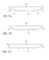
- the regioncan be a flattened region, a sloped region, or a plateau shaped region having a plateau top and two sloped sides, wherein each sloped side forms about 10-15 degree angle to a surface of the substrate.
- the region's configurationdepends on configuration of the gradually sloping edge and the alignment of the frames with respect to the embossing die.
- One embodimentpertains to a method, which comprises providing a web substrate and passing the web substrate under or over an embossing die.
- the embossing dieis configured to move up or down with respect to the substrate to create recessed regions in an area of the web substrate.
- the embossing diecomprises protruding features configured to create the recessed regions.
- the embossing diealso comprises a left side edge and a right side edge in which, at least one of the left side edge and the right side edge is a gradually sloping edge.
- the methodfurther includes forming the recessed regions into a first area of the web substrate, advancing the web substrate so that a second area of the web substrate can be formed with the recessed regions, and forming the recessed regions into the second area.
- the methodfurther includes aligning the embossing die over the web substrate such that between the first area and the second area, a region is formed wherein the region has a controlled configuration.
- the controlled configurationcan be a gradually slope plateau configuration having a flattened top side and two sloped sides, each of the two sloped sides forming a 10-15 degree angle to a surface of the substrate; a flattened region; or a sloped region with a maximum vertical height of less than 100 ⁇ m.
- One embodimentpertains to a method, which comprises providing a plurality of substrates.
- the substratesincludes at least differently treated substrates, different substrates, substrates made of different materials, substrates comprises of different materials, and substrates intended to used for different types of devices. Further, the method includes forming recessed regions in each of the substrates. The recessed regions on one of the substrates need not (but can be) similar or exactly like recessed regions on another one of the substrate.
- An embossing dieis used to form the recessed regions in at least one of the plurality of substrates. The embossing die comprises protruding features configured to create the recessed regions, a left side edge, and a right side edge.
- the methodincludes joining the plurality of substrates together to form a roll of substrate and performing one or more Fluidic-Self Assembly processes on the roll of substrate to deposit a plurality of functional blocks into the recessed regions.
- the plurality of functional blocksmay be of same types or different types of functional blocks.
- An example of Fluidic Self-Assembly (FSA)is described in U.S. Pat. No. 6,864,570, entitled “Method for fabricating self-assembling microstructures,” which is incorporated by reference herein.
- FIG. 1illustrates an example of a functional component block
- FIG. 2Aillustrates an exemplary embodiment of an electronic assembly with the functional block deposited therein
- FIGS. 2B-2Cillustrate exemplary embodiments of a via formed in a dielectric layer
- FIGS. 2D , 2 E(a)- 2 E(b) and, 2 Fillustrate exemplary embodiments of a conductive interconnect coupling to a functional block
- FIG. 2Gillustrates an exemplary embodiment of incorporating the assembly formed in FIG. 2A to a second substrate (a device substrate);
- FIG. 3illustrates an exemplary embodiment of an electronic assembly with the functional block deposited therein and the substrate being multi-layered;
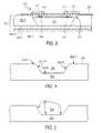
- FIGS. 4-5illustrate aspects of a recessed region formed in a substrate
- FIG. 6Aillustrates an exemplary embodiment of an electronic assembly with multiple functional blocks deposited therein
- FIG. 6Billustrates an exemplary embodiment of an electronic assembly with multiple functional blocks deposited therein with the functional blocks being recessed below a surface of the substrate;
- FIGS. 7A-7Dillustrate what happens to a substrate when a template with a straight edge is used to create recessed regions in the substrate
- FIGS. 7E-7Fillustrate non-uniform or inconsistent step-changes between frames of a substrate
- FIGS. 7G-7Hillustrate an exemplary embodiment of the present invention with consistent step-changes between frames of a substrate
- FIGS. 7I-7Millustrate an exemplary embodiment that uses a roller with features to create recessed regions in a substrate
- FIGS. 8A-8Fillustrate an exemplary embodiment of an embossing die with gradually sloping edges that can be used to make recessed regions in a substrate in accordance to embodiments of the present invention
- FIGS. 9A-9Eillustrate an exemplary embodiment of an embossing die with gradually sloping edges that can be used to make recessed regions in a substrate in accordance to some embodiments of the present invention
- FIGS. 10A-10Gillustrate another exemplary embodiment of an embossing die with gradually sloping edges that can be used to make recessed regions in a substrate in accordance to embodiments of the present invention
- FIGS. 11A-11Cillustrate more exemplary embodiments of embossing dies with gradually sloping edges that can be used to make recessed regions in a substrate in accordance to embodiments of the present invention
- FIGS. 12-13illustrate exemplary embodiments of various overall processes of making an electronic assembly with functional block in accordance to embodiments of the present invention
- FIGS. 14-15illustrate an exemplary embodiments of forming a roll or a long sheet of substrate comprising of various different types of substrates or differently treated substrates joined together;
- FIGS. 16-17 , 18 A- 18 B and 19illustrate exemplary methods of making an electronic assembly with functional block in accordance to embodiments of the present invention.
- Embodiments of the present inventionrelate to methods for forming holes, openings, or recessed regions in a substrate or web substrate and depositing functional blocks into the recessed regions, forming layers, and/or electrical interconnections to the blocks to form electronic assemblies.
- the disclosurerefers to the substrate with one or more functional blocks deposited therein as a “strap assembly.”
- Electronic devices that can be formed using embodimentsinclude a display, a smart card, a sensor, an electronic tag, an RFID tag, etc.
- Some embodiments of the present inventionalso relate to devices and methods that are used to form recessed regions in the substrate for functional blocks to be deposited therein.
- Some embodiments of the present inventionalso relate to feature dimensions and specifics of the functional blocks with respect the substrate and the recessed regions.
- the following description and drawingsare illustrative of the invention and are not to be construed as limiting the invention.
- Embodiments of the inventionapply to both flexible and rigid substrates, as well to both monolayer and multilayer substrates.
- the substrateis able to receive a functional block or functional blocks that may have a circuit element thereon.
- the substrateincludes one functional block.
- the substrateincludes a plurality of such recessed regions for a plurality of such functional blocks.
- the blocksare contained in a slurry, which is deposited onto the flexible substrate as is typically done in a Fluidic Self-Assembly (FSA) process.
- FSAFluidic Self-Assembly
- the substratemay still be flexible because the size of these blocks (e.g., 650 ⁇ 500 microns or 850 ⁇ 850 microns) is small or significantly small in comparison to the flexible substrate (e.g., 3 ⁇ 6 mm or even larger).
- the flexible substrateforms part of an RFID tag, a merchandise label, a pharmaceutical label/seal, or a display backplane, to name a few example applications.
- a strap substrateis fabricated with one or more recessed receptor sites, and one or more functional or integrated circuit blocks are deposited into the recessed receptor sites, for example, using a Fluidic Self-Assembly (FSA) process.
- FSAFluidic Self-Assembly
- the functional blocksmay be deposited by one or more FSA operations, by robotic pick-and-place operations, or by other methods.
- the strap substrateis then attached to another substrate, which may comprise a set of patterned or printed conductor.
- the conductorcan be an electrical element of a device, for instance, the conductor can be elements or parts of an antenna for an RFID device. More than one functional block may be deposited into a strap substrate depending on application.
- a strap assemblyis formed when one or more functional blocks are deposited in the strap substrate and other elements (e.g., dielectric layer and electrical interconnection) formed thereon.
- the overall manufacturing process of a strap assemblyimpacts the cost of the final device that incorporates the strap assembly. For example, when a strap assembly is formed using a web process, efficiencies of the block deposition, dielectric film formation, material usage, or electrical interconnection fabrication play important roles in the final device cost and performance.
- FIG. 1illustrates exemplary embodiments of an object that is functional component block 1 .
- the functional block 1can have various shapes and sizes.
- Each functional block 1has a top surface 2 upon which a circuit element is situated (not shown).
- the circuit element on the top surface 2may be an ordinary integrated circuit (IC) configured for any particular function.
- the ICmay be configured to drive a pixel of a display.
- the ICmay also be configured to receive power from another circuit, such as an antenna, and perform a particular function or functions for the operation of a passive RFID tag.
- the ICmay be configured to receive power from an energy source (e.g. battery) for the operation of an active RFID tag.
- an energy sourcee.g. battery
- the functional block 1also includes a contact pad 3 (one or more contact pads 3 ) to allow electrical interconnection to the circuit element on the block 1 .
- the functional block 1can have a trapezoidal, rectangular, square, cylinder, asymmetrical, or symmetrical shape. The top of the block 1 is often (but need not be) wider than the bottom of the block 1 .
- Each functional block 1may be created from a host substrate and separated from the host substrate. Methods of making a functional block 1 are known in the art and for instance, can be found U.S. Pat. Nos. 5,783,856; 5,824,186; 5,904,545; 5,545,291; and 6,291,896, which are hereby incorporated by reference in their entireties.
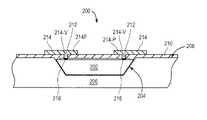
- FIG. 2Aillustrates a cross-sectional view of an exemplary embodiment of an electronic assembly (or a strap assembly) 200 .
- the assembly 200can be part of or made to incorporate into a display device, a RFID tag, a merchandise label (a CD label), a pharmaceutical label or bottle, etc.
- the assembly 200can be attached to another substrate (e.g., a device substrate) that may have patterned, printed, or formed thereon a conductor or conductors.
- a functional block 202is deposited in recessed region 204 of a substrate 206 to form the assembly 200 .
- the functional block 202can be the functional block 1 previously discussed. Methods of making a functional block are known in the art.
- the functional block 202is a NanoBlockTM made by Alien Technology.
- the functional block 202is recessed below a surface 208 of the substrate 206 .
- the functional block 202is recessed sufficiently below the surface 208 to provide sufficient space for electrical connection to the functional block 202 .
- the functional block 202is deposited into the recessed region 204 using a Fluidic Self-Assembly (FSA) process.
- FSAFluidic Self-Assembly
- the surface 208 of the substrate 206is the native surface of the substrate 206 before any deposition of any other materials on top of the surface 208 .
- the substrate 206may be a flexible substrate made out of plastic, fabric, metal, or some other suitable materials.
- the substrate 206is flexible.
- the substrate 206is flexible.
- the assembly 200is flexible.
- a dielectric layer 210is formed over the surface 208 and over the functional block 202 .
- the dielectric layer 210in many instances, also functions as a planarization layer as well as a layer that traps or keeps the functional block 202 in the recessed region 204 .
- Vias 212are also formed into the dielectric layer 210 to expose portions of the functional block 202 .
- each of the exposed portions of the functional block 202comprises a contact pad 216 that enables electrical interconnection to the functional block 202 .
- the functional block 202includes two contact pads 216 placed on opposite sides and/or diagonal to each other.
- the dielectric layer 210has two vias 212 , one for each contact pad 216 .
- each via 212exposes some or all of the top area 216 -A of the corresponding contact pad 216 ( FIGS. 2B-2C ).
- each via 212has a diameter that is smaller than the top area 216 -A of the corresponding contact pad 216 .
- the via 212has a cone-like shape where the via 212 has a top diameter and a bottom diameter. The bottom diameter is smaller than the top diameter. Additionally, the bottom diameter is at least 20% smaller than the contact pad 216 .
- the diameter of the via 212 at the bottomshould be no more than 80% of the width of the contact pad 216 , which may be defined by the area 216 -A.
- the via 212has a non-symmetrical cone-like shape in which one side of the via 212 has a flatter or gentler slope than the other side ( FIG. 2C ). As shown in FIG. 2C , the via 212 has two sides, 212 -A and 212 -B, in which the side 212 -B has a more “gentle” or flatter slope than the side 212 -A. In one embodiment, a small protrusion 212 -C is formed on the side 212 -B of the via 212 . The configuration of the via 212 in accordance to the present embodiment helps the conductive material to more easily fill the via 212 .
- the dielectric film 210is deposited using a roll-to-roll process over the substrate 206 that has the functional block 202 deposited therein.
- the dielectric film 210may be deposited using methods such as lamination of a polymer film or coating of a liquid layer over the substrate 206 and subsequent curing to form the dielectric film 210 .
- the dielectric film 210is deposited by a wet coating process, such as comma coating, or by a direct writing process, and subsequently dried or cured.
- the dielectric film 210may be necessary in embodiments where the assembly 200 is used for devices such as RFID tag since the dielectric film 210 provides good RF performance for the RFID tag.
- the dielectric film 210contains at least one opening formed through the dielectric film for the via 212 .
- Each via 212enables the conductive interconnect 214 formed on the top of and into the dielectric film 210 to make electrical connection with a contact pad 216 on the functional block 202 .
- Each conductive interconnect 214can be one conductor or two conductors joined together.
- the conductive interconnect 214can be formed in a one-step process or a two-step process.
- one conductoris referred to as a “via conductor” ( 214 -V) since it fills the via 212 .
- the other conductoris referred to a “pad conductor” ( 214 -P) which sits on a portion of the dielectric layer 210 and connects or joins the via conductor 214 -V.
- Each via 212 in the dielectric film 210is positioned over a contact pad 216 , such that the via 212 enables interconnection from the contact pad 216 on the functional block 202 to the interconnect 214 .
- each via 212is formed such that no dielectric material is present in the via 212 .
- the number of vias 212can be increased or decreased depending on the product.
- the number of vias 212also depends on how many contact pads 216 are present in the functional block 202 or depending on how many electrical connection is needed. For example, many more dielectric vias may be needed for embodiments where the assembly 200 is incorporated into display driver or sensor applications.
- the dielectric film 210has two vias 212 which are also situated diagonally to each other over the corresponding contact pads 216 .
- the dielectric film 210has a thickness ranging from about 5 ⁇ m to about 60 ⁇ m. In another embodiment, the thickness of the dielectric film 210 is approximately 38 ⁇ m.
- the dielectriccan be either a wet film that is dried or cured, or as a dry film that is laminated onto the substrate 206 .
- the dielectric film 210has an adhesive functionality to the side that is applied to the substrate 206 .
- the adhesive functionalitycould be an inherent property of the dielectric material or its application process, or it could be due to an adhesive film that is applied to the side of the dielectric film 210 that comes in contact with the substrate 206 .
- the adhesive filmis non-conductive and can be processed to achieve the desired structure for the via 212 .
- the adhesive filmmust be photo imageable or laser drillable to allow the via 212 to be formed.
- a laser drillable adhesive filmcould be fabricated by using an adhesive that inherently absorbs UV light, or else by using an adhesive formulation that consists of a UV-absorbing species. If an adhesive film is used on the dielectric film 210 , all of the dimensions listed for the dielectric film 210 , including film thickness and via diameter, applies to the dielectric and adhesive film combined together.
- the dielectric film 210has a coefficient of thermal expansion (CTE) that is closely matched to that of the substrate 206 .
- CTEcoefficient of thermal expansion
- the CTEis within ⁇ 20 ppm/° C. of the CTE of the base material of the substrate 206 , which is typically 50-70 ppm/° C., but can vary depending on the substrate.
- the proximity of the dielectric film CTE to the substrate CTSis more important than the absolute value of the substrate CTE.
- Suitable dielectric materialsinclude, but are not limited to polyimide, polyetherimide, liquid crystal polymer, and polyethylenenaphthalate.
- the vias 212 in the dielectric film 210are formed over corner areas of the functional block 202 . In one embodiment, the vias 212 are only formed over the corners of the functional blocks with the contact pads 216 . Additionally, the dielectric film 210 may also be formed only in discrete or selected positions on or around the functional block 202 and around the area of the substrate 206 that has the functional block 202 deposited therein. When the dielectric film 210 is discretely or selectively formed, the vias 212 may not be necessary since the dielectric material may be selected to not form over the contact pads 216 to leave the contact pads 216 exposed.
- a method that can be used for selectively or discretely form the dielectric film 210includes direct write, such as ink-jet, and laser assisted deposition, etc. Such method enables the deposition of the dielectric film 210 anywhere the material is needed. Additionally, such selective deposition of the dielectric film 210 enables customizing deposition of the dielectric film for uses such as bridging or covering the gap from the functional block 202 to the substrate surface 208 , and/or to protect sensitive areas on the functional block 202 . Such selective deposition of the dielectric film 210 minimizes the use of the dielectric material where it is not needed. Other methods that can be used for selectively or discretely form the dielectric film 210 include patterning, etching, and photolithography.
- the dielectric layeris disposed between the functional block which can be an integrated circuit (IC) for a device and the conductive interconnect or conductive traces which could be use to connect the functional block to an external electronic element such as an antenna.
- the via formed through the dielectric layerprovides a direct electrical connection to the IC, but there is still a capacitive coupling between other parts of the functional blocks and the external electronic element. It is disadvantageous to have such capacitive coupling between the IC and the conductive traces, and this capacitive coupling is increased due to proximity of the conductive traces to the IC. Placing the dielectric layer between the functional block and the external electronic element provides some vertical distance between them.
- low-dielectric constant materialsinclude porous materials, fluorinated materials, and silicon-rich materials.
- each conductive interconnect 214 formed on top of and into the dielectric layer 208fills a particular vias 212 so as to establish electrical interconnection to the functional block 202 .
- each conductive interconnect 214constitutes both a via conductor 214 -V as well as a pad conductor 214 -P.
- the conductive materialcovers all of the exposed area of the contact pad 216 that is exposed by the via 212 .
- the conductive interconnect 214constitutes a conductive trace of an antenna element or acts as an interconnect for an antenna element.
- the conductive interconnect 214can also interconnect the functional block 202 to an external electrical element or elements (e.g., antennas or electrodes).
- the conductive interconnect 214can also be an electrical or conductive lead from the external electrical element.
- the conductive interconnect 214is formed using a roll-to-roll process.
- materials used to form the interconnect 214is deposited onto and into the dielectric layer 208 as the substrate 208 is processed on a web line.
- Material used to make the conductive interconnect 214may be selected such that it can be cured, for example, by heat or by electromagnetic radiation, or by ultraviolet radiation, and can be used in the roll-to-roll process.
- the interconnect 214 materialis cured as the substrate 206 is processed on a web line.
- the conductive interconnect 214is made of a conductive composite of conductive particles in a non-conductive matrix, such as silver ink.
- the conductive interconnect 214is made of metal or metals that are evaporated onto the substrate 206 or onto the dielectric layer 210 , over the corresponding via 212 , and subsequently patterned.
- the conductive interconnect 214can also be comprised of an organic conductor, or composites of carbon nanotubes or inorganic nanowires dispersed in a binder.
- the conductive interconnect 214is made of a conductive composite, such as silver ink or silver-filled epoxy that completely filled by the corresponding vias 212 .
- the conductive interconnect 214is made of one or more of the following: conductive particles dispersed in a nonconductive or an organometallic matrix (e.g., silver ink), sputtered or evaporated metal, conductive carbon composite, carbon nanotubes, inorganic nanowires dispersed in a nonconductive matrix, and any of these materials combined with metallic nanoparticles.
- the conductive interconnect 214comprises a nonconductive matrix that consists of a thermoplastic polymer, a thermoset polymer, or a B-staged thermoset polymer.
- the elastic modulus of a conductive composite that is used to form the conductive interconnect 214is between 120,000 psi and 60,000 psi.
- the resistivity of the conductive interconnect 214is less than 76 m ⁇ /square/mil, more optimally, less than 60 m ⁇ /square/mil, even more optimally less than 42 n ⁇ /square/mil, and most optimally less than 25 m ⁇ /square/mil.
- the conductive interconnect 214is made of a material that is able to maintain good electrical contact to the top-most conductive feature or features (e.g., the contact pad 216 ) on the functional block 202 , such that the combination of the substrate 206 , the functional block 202 , the dielectric layer 210 , the contact pad 216 , and the conductive interconnect 214 is able to maintain sufficient electrical contact throughout, with less than a 10% variation in total resistance.
- the combination of the substrate 206 , the functional block 202 , the dielectric layer 210 , the contact pad 216 , and the conductive interconnect 214is able to maintain sufficient electrical contact throughout, with less than a 10% variation in total resistance, when the assembly 200 is subjected to thermal cycles for 100 times from ⁇ 40° C. to 85° C., and bent over a 1-inch-diameter mandrel for 80-100 times.
- Each conductive interconnect 214can partially or completely cover the corresponding via 212 for the conductive material in the via 212 to make electrical contact to the functional block 202 or the corresponding contact pad 216 on the functional block 202 .
- the conductive interconnects 214also have a good adhesion to the dielectric film 210 , such that the interconnects can survive flexing over a 1-inch mandrel as previously mentioned.
- the conductive interconnect 214is coupled to another conductive trace (not shown) that may be formed on the substrate 206 .
- conductive tracecan be an antenna trace, for example, when the assembly 200 is to be incorporated into an RFID tag.
- the conductive interconnect 214also forms the conductive trace for the final device itself.
- the conductive interconnect 214can also be part of an antenna element for an RFID tag.
- the conductive interconnect 214 and the conductive tracecould be combined as one material applied in one process, or as two materials applied in two sequential steps.
- the interconnect 214constitutes a via conductor 214 -V and a pad conductor 214 -P connecting to a particular contact pad 216 .
- the via conductor 214 -Vcontacts the conductive pad 216 on the functional block 202 at the bottom of the via 212 . It is preferable that the via conductor 214 -V covers all of the contact pad 216 that is exposed by the via 212 .
- the top diameter or the top area of the via conductor 214 -Vis larger than the top diameter of the corresponding via 212 . In one embodiment, the top diameter or the top area of the via conductor 214 -V is about 1-3 times larger than the top diameter of the via 212 . In another embodiment, top diameter or the top area of the via conductor 214 -V is 1-2 times larger than the top diameter of the via 212 .
- the pad conductor 214 -Pprovides a large or larger conductive area for fast electrical attachment of the assembly 200 to a conductor on another electrical functional element, such as a RFID antenna, a display driver strip, or a sensor assembly.
- the pad conductor 214 -Pis at least (1 mm) ⁇ (1 mm) large. Since this interconnection area is larger than the connection or contact pad 216 on the functional block 202 , lower-cost, lower-precision equipment can be used to produce electrical contact between the assembly 200 and other functional elements such as antennas.
- the pad conductor 214 -Pmay be made of the same material or different material as the via conductor 214 -V.
- the pad conductor 214 -Pmust make electrical contact with any necessary conductive material in the via 212 (e.g., the via conductor 214 -V) as well as the corresponding contact pad 216 that may be provided on the functional block 202 .
- the conductive interconnect 214may have several layouts. Exemplary layouts are shown in FIGS. 2D-2F , below. The layouts in FIGS. 2D-2F illustrate exemplary configurations for the pad conductor 214 -P of the conductive interconnects 214 . It is to be noted that other configurations are also feasible.
- the assembly 200includes more than one interconnections 214 and more than one pad conductor 214 -P.
- a “bow-tie” configuration 214 Ais provided.
- two pad conductors 214 -Pform a bow tie like configuration.
- the configuration 214 -Aincludes two pad conductors 214 -P, each of which having two fingers 244 coming out of each pad conductor.
- the fingers 244are able to make contact with each of the contact pad 216 at any of the 4 corners of the functional block 202 .
- Each finger 244would make contact to a contact pad 216 that is closest to the corresponding finger 244 .
- each finger 244overlaps the functional block 202 or a contact pad 216 provided on the block 202 .
- the finger 244is less than or equal to the top diameter of the corresponding contact pad 216 that the finger 244 connects to.
- the finger 244covers a portion of the via conductor that connects to the contact pad 216 . In one embodiment, the finger 244 covers all of the via conductor that connects to the contact pad 216 .
- the bow-tie configuration 214 Aenables the conductive interconnect 214 to make contact to the functional block 202 where the contact pads 216 is placed on any of the four corners of the functional block 202 . It may be that the functional block 202 has one contact pad 216 . Thus, not all of the fingers 244 would contact a contact pad 216 .
- the functional block 202thus can also be deposited into a receptor 204 in a manner where the contact pads 216 can be oriented at any corner and still able to allow contact from the fingers 244 to the contacts pads 216 .
- FIG. 2Eanother “bow-tie” configuration 214 B, which does not have the fingers 244 shown in the bow-tie configuration 214 A is provided. Instead, in the bow-tie configuration 214 B, sides 246 are provided on the pad conductors 214 -P where each of the sides 246 runs across almost the length of each side of the functional block 202 . In this configuration, two pad conductors 214 -P also form a bow tie-like configuration over parts of the functional block 202 . In the present embodiment, each of the sides 246 is placed in contact with a contact pad 216 on the functional block 202 .
- FIG. 2Fillustrates an exemplary embodiment of a configuration of the conductive interconnect 214 or the pad conductor 214 -P with a non-bow-tie configuration 214 C.
- the functional block 202may have contact pads 216 placed diagonally to each other.
- the configuration 214 Cis similar to the configurations 214 A and 214 B above except that only one arm is necessary on each pad.
- the configuration 214 Cis configured with two pad conductors 214 -P each having an arm or extension 248 to make connection to one of the contact pads 216 .
- the arm 238allows the conductive interconnect 214 to contact the functional block 202 with minimal conductive material over the functional block 202 .
- Other configurations or shape for the extension 248are possible.
- the configuration 214 Cis especially useful when the functional block does not have rotational symmetry that is greater than two folds.
- the contact pads 216are shown to contact the fingers 244 or the sides 246 of the pad conductor.
- the dielectric layer 210may be formed over the block 202 and the vias 212 are created in the dielectric layer 210 so that the contact pads 216 are exposed.
- the viasare filled with conductive interconnects 214 or via conductors 214 -V as previously mentioned.
- the viacould also be filled by the same material and at the same time as the sides 246 are formed.
- the fingers or sides from the pad conductors 214 -Pcover at least a portion of the corresponding via conductors 214 -V to establish interconnection to the contact pads 216 .
- the vias 212 and the via conductors 214 -Vare not shown in FIGS. 2D-2F .
- each pad conductor 214 -Phas a resistivity that is less than 25 m ⁇ /square/mil, optimally less than 18 m ⁇ /square/mil, and most optimally less than 12 m ⁇ /square/mil.
- each part of the pad conductor part 214 -P that is over the via conductorshould be no wider than 2 times the smallest diameter of the corresponding via conductor 214 -V, optimally no wider than 1.5 times the diameter of the via conductor 214 -V, and more optimally, the same width as the widest diameter of the via conductor 214 -V.
- the assembly 200 shown in FIG. 2Acan be referred to as a strap assembly.
- the strap assembly 200is further coupled or attached to another device for form a final device (for example, to form an RFID tag).
- FIG. 2Gillustrates a cross-sectional view of the strap assembly 200 being attached to a second substrate or a device substrate 201 .
- the substrate 201may include other active elements and/or electrical components and in one embodiment, includes a conductor pattern 203 formed thereon.
- the conductor pattern 203is part of an antenna element that can be used for an RFID device.
- the substrate 206is “flipped” over such that the surface 208 is facing the second substrate 201 and the conductor pattern 203 .
- the substrate 206is attached to the second substrate 201 in a way that the conductor pattern 203 is coupled to the interconnects 214 .
- Conductive adhesivesmay be used to facilitate the attachment of the strap assembly 200 to the substrate 206 .
- Other sealing materialscan also be added.
- the substrate 206is a monolayer plastic film such as the substrate 206 shown in FIG. 2A .
- a plastic monolayer base filmcan be a thermoset or an amorphous or semicrystalline thermoplastic plastic film.
- the substrate 206is a thermoplastic base film and has a glass transition temperature (Tg) of at least about 100° C., more optimally at least about 125° C., and even more optimally at least about 145° C.
- Tgglass transition temperature
- the thermoset plastic filmcan be selected from UV-curable, moisture-curable, and heat-curable thermoset plastic films.
- Example of suitable materials that can be used for the substrate 206include, but are not limited to, polyethylene, polystyrene, polypropylene, polynorbornene, polycarbonate, liquid crystal polymer, polysulfone, polyetherimide, polyamide, polyethyleneterephthalate, and polyethylenenaphthalate, and derivatives thereof.
- the substrate 206comprises multiple layers for example, layers 206 A- 206 D, with the recessed regions 204 formed in one (or more) of the layers, e.g., the top layer 206 A and with the additional layers used to provide one or more of dimensional stability, mechanical strength, dielectric properties, desired thickness, functionalities, etc. ( FIG. 3 ).
- the substrate 206is made of a material that minimizes positional distortion of the recessed region 204 after the substrate 206 is subjected to a first thermal excursion for about 30 minutes at about 125° C. Prior to assembling the functional block 202 into the recessed region 204 , the substrate 206 is subjected to at least one thermal excursion cycle for about 30 minutes at about 125° C. During this thermal excursion cycle, the recessed region 204 that is formed into the substrate 206 may be distorted positionally. The position of the recessed region 204 on the substrate 206 may move or be distorted slightly due to the heat or change of material characterization due to heat.
- the substrate 206must be made of a material that will cause only about 30-500 ⁇ m, more optimally, 30-300 ⁇ m, positional distortion to the location of the recessed region 204 that is formed on the substrate 206 .
- Positional distortionrefers to the location of the recessed region 204 being moved positionally from the originally created position on the substrate 206 .
- the substratehas a length of about 200 mm along which the distortion is measured.
- the substrate 206is made of a material that when subjected to a first thermal excursion causes the recessed region to be move by only about 30-500 ⁇ m, or 30-300 ⁇ m.
- the substratecould have a length that is about 300 mm or 500 mm long, and the allowance distortion along such a length would scale linearly with the distortion allowed along a shorter length.
- areas around the area where the recessed region 204 is to be formedis maintained at a temperature between about 50° C. and the glass transition temperature of the substrate material. Such temperature control minimizes distortion to the substrate 206 as the recessed region 204 is being formed.
- the recessed region 204is at least as large as the functional block 202 that fills the recessed region 204 . More optimally, the recessed region 204 is slightly larger (e.g., 0-10 ⁇ m or 1-10 ⁇ m) than the functional block 202 in width, depth, and length, and has a sloping sidewall similar to that of the shaped functional block 202 . In general, the recessed region matches the shape of the functional block. If the functional block 202 is square, the recessed region 204 is also square, and if the functional block 202 is rectangular, the recessed region 204 is also rectangular.
- the substrate 206is substantially flat, especially in or near the recessed region 204 .
- Substantially flatis characterized by surfaces of the substrate having no protrusion or no protrusion greater than 5 ⁇ m. In other words, if there are any protrusions at all, the protrusion is not greater than 5 ⁇ m, thus giving the substrate 206 a substantially flat characteristic.
- FIG. 4illustrates an exemplary embodiment of the substrate 206 with a top surface 208 that is substantially flat. The substrate 206 only needs to have its top surface 208 (or alternatively, the top surface of the top layer of the substrate 206 when the substrate includes multiple layers) being substantially flat. As shown in FIG. 4 , the sides of the recessed region 204 are substantially flat as well.
- top sides 204 -T, bottom side 204 -B, and sidewalls 204 -W of the recessed region 204are substantially flat with no protrusion.
- FIG. 5illustrates an exemplary embodiment of the substrate 206 with some minor protrusions 220 along a surface of the substrate 206 . Nevertheless, the protrusions 220 are so minor that the substrate 206 still has the substantially flat characteristic and that the recessed region 204 has sides that are substantially flat.
- the recessed region 204has a width-depth aspect ratio that is configured to substantially match a width-depth aspect ratio of the functional block 202 .
- the recessed region 204has a width-depth aspect ratio that is less than 14:1, optimally, less than 10.5:1, and even more optimally, less than 7.5:1.
- the functional block 202thus has a similar width-depth aspect ratio.
- the substrate 206is also selected so that the substrate has a good thermal stability to withstand standard processing.
- the material of the substrate 206is such that the substrate 206 allows the recessed region 204 to maintain the same positional accuracy requirements previously mentioned.
- the substrate 206is made of a material that is able to allow the recessed region 204 to maintain its positional accuracy after going through a 125° C.-150° C. thermal excursion.
- the assembly 200is cut, sliced, separated, or singulated from a plurality of web-assembled assemblies as will be described below.
- a plurality of assemblies 200can be formed in one short time frame.
- a roll-to-roll processcan be used.
- a web substrateis provided.
- the web substratemay be a continuous sheet of web material which when coiled, is a roll form.
- a plurality of recessed regions 204are formed into the web material using embodiments of the present invention, which will be described below.
- a plurality of functional blocks 202are deposited into the recessed regions 204 on the web substrate (e.g., using an FSA process) to form a plurality of the assemblies 200 shown in FIG. 2A .
- Areas or strips of the web substratecan later be sliced, singulated, cut, or otherwise separated to produce individual assemblies 200 .
- a web sheet having a plurality of assemblies 200is attached to another web substrate similarly to previously described in FIG. 2G .
- Individual devicescan then be formed by slicing or singulating after the substrates are adhered to one another as illustrated in FIG. 2G .
- FIGS. 6A-6Billustrate an assembly 400 that includes several assemblies formed similarly to the assembly 200 .
- the assembly 400is similar to the assembly 200 above except when multiple assemblies are formed on one piece of substrate material.
- a substrate 406includes a plurality of recessed regions 404 formed therein. Each recessed region 404 includes a functional block 402 deposited therein.
- the assembly 400is also similar to the assembly 200 shown above except that there are more of the functional blocks deposited in the substrate. Singulating areas of the substrate 406 after the functional blocks 402 have been deposited and other elements formed thereon can produce a plurality of assemblies 200 shown above.
- the substrate 406can be a web substrate, a frame of a web substrate, a section of a web substrate, or a sheet substrate.
- each of the functional blocks 402should account for any contact pads on top of the functional block 402 .
- a substantial amount of the plurality of functional blocks 402are recessed below a top surface 406 -T of the substrate 406 .
- the gap 408is between about 0-10 ⁇ m.
- the substantial amount of the functional blocks 402 being recessed below the surface of the substrate 406is defined by (1) less than 10% of the plurality or the population of the functional blocks protrudes above the top surface 406 -T of the substrate 406 ; (2) less than 1% of the plurality of the functional blocks 402 protrude above the top surface 406 -T of the substrate 406 ; (3) more than 90% of the plurality of the functional blocks 402 are recessed below the top surface 406 -T of the substrate 406 ; or (4) more than 99% of the plurality of the functional blocks 402 are recessed below the top surface 406 -T of the substrate 406 .
- the populations of the depths 404 -R of the recessed regions 404 and the thicknesses 402 -D of the functional block thicknesscan be represented by distribution with an average thickness or depth ( ⁇ r or ⁇ N, respectively) and a standard deviation ( ⁇ r or ⁇ N, respectively).
- ⁇ c ⁇it is desirable to have ⁇ c ⁇ . More preferably, using the equations above and applying Normal statistics, it is preferable to have ⁇ c and ⁇ such that less than 10%, or more preferably less than 1%, of the plurality of the functional blocks 402 protrude above the top surface 406 -T of the recessed regions 404 .
- the assembly 400is characterized by in that the locations of the recessed regions 405 on the substrate 406 have a good positional accuracy. In one embodiment, across a 158 mm-wide area of the substrate 406 , the positional accuracy of each recessed region 404 is within 100 ⁇ m at 3 ⁇ , in another embodiment, within 50 ⁇ m at 3 ⁇ , and in another embodiment, within 30 ⁇ m at 3 ⁇ . These positional accuracy numbers also scale linearly with the width of the substrate 406 . For example, when the substrate 406 has a width of about 316 mm the positional accuracy of the recessed regions 404 is within 200 ⁇ m at 3 ⁇ . Similar to the assembly 200 , the assembly 400 includes a dielectric film formed over the functional blocks 402 , vias formed in the dielectric film to expose contact pads on the functional blocks 402 , and conductive interconnections to establish electrical connections to the functional blocks 402 .
- the substrate 206 or 406 with recessed regions previously describedcan be processed using various exemplary methods and apparatuses of the present invention to form the recessed regions.
- a template with protruding structuresis used to create recessed regions in a substrate.
- the templateis pressed against the substrate to create recessed regions or holes in the substrate.
- an embossing dieis used to form a plurality of recessed regions in a substrate.
- the embossing dieis configured to form a gradual ramp in the substrate at specified area of the substrate.
- a specified area of the substratecan be referred to as a frame of substrate in which an array or arrays of recessed regions are formed. See for example FIG. 6A , the substrate 406 can be referred to as a frame of substrate with an array of recessed regions 404 and functional blocks 402 .
- the embossing diealso forms a gradual ramp between each two frames of substrates. The gradual ramp thus defines and separates one frame from another frame.
- embossing processes used to form the recessed regionsutilize hot embossing processes where an embossing die with protruding features is pressed into a substrate.
- the embossingis performed at an elevated temperature so that the substrate can be soft or hot in order for the recessed regions to be easily formed into the substrate.
- the embossing dieis forcibly pressed into the heated substrate causing the substrate material to flow locally around and into features of the embossing die. While such processes can accurately produce a negative image of the die features with relative ease, it is difficult to control the depth to which the edges of the embossing die presses into the substrate.
- FIGS. 7A-7Dillustrate the concept stated above.
- FIG. 7Ashows an embossing die 51 with protruding structures 52 and straight edges 60 .
- the protruding structures 52may vary in shapes and sizes depending upon the object that is to be placed into a substrate or web material.
- FIG. 7Bshows the embossing die 51 facing one side of a substrate 50 .
- FIG. 7Cshows the embossing die 51 contacting the substrate 50 and the protruding structures 52 from the template 51 pierce or press into the substrate 50 .
- the straight edges 60also contact the substrate 50 and may penetrate the substrate to a certain depth.
- step-changes 57 and 59are formed at or around the area of the substrate that the straight edges 60 contact the substrate 50 .
- the step-changes 57 and 59are often not uniform or continuous in the same direction from frame to frame. These step-changes 57 and 59 can interrupt the flow of the functional blocks during the FSA process or can cause problems in subsequent lamination and/or deposition processes and therefore are detrimental to the processes.
- FIG. 7Eillustrates a cross-sectional view of an example of step-changes created between frames of a web substrate 50 using an embossing process such as the one described above. Similar step-changes can also be caused by processes such as roll-to-roll and continuous processing. For example, a continuous belt that may be present in the processing may very well cause similar step-changes.
- step-changes 72are formed between each two frames 74 of the web substrate 50 . As can be seen, the step-changes 72 are not uniform or continuous in the same direction from frame to frame.
- step-changescan include channels or indentations 76 that are formed between frames 74 . These types of step-changes should be avoided in the web substrate. These step-changes 72 or 76 unpredictably interrupt the flow of the functional blocks during the FSA process, and therefore are detrimental to the process.
- a step-change between framesmay be acceptable in the web substrate if the step change is always in the same direction. That way, the FSA process can be controlled or monitored accordingly to a predictable presence of a step-change that is always in the same direction for an entire web or section of substrate.
- a step-changeis created into the web substrate such that when examining the space between two frames on the web substrate, there is a step going from one frame to the next, and that the step can be configured to always be higher on the left side, or always higher on the right side, or always in the same direction.
- a web substrate 76is formed such that there are a plurality of frames 74 . Each frame 74 is separated from another frame by a step-change 78 .
- the step-change 78is consistently in the same direction from one frame 74 to the next frame 74 .
- Figure Hillustrates another example of a consistent or uniform step-change between two frames of the web substrate 76 .
- One advantage of the consistent step-changeis that the flow of FSA slurry is not disrupted by the step-changes 78 unexpectedly and thus, the FSA process can be more controlled.
- a template or mold used to create the recessed regionsmay incorporate a feature that creates such a step-change in the web substrate.
- an embossing die with gradually sloping edgesincludes the necessary features to form recessed regions on a substrate and also include one or more gradually sloping edges wherein the vertical extent of the slope exceeds the maximum depth of the embossing or penetration depth.
- the embossing dieembosses a gradually sloping perimeter around each frame of the substrate.
- the edgescan also be configured so that the angle and contour of the slope create a gradual ramp at a perimeter of each frame of the substrate.
- the edgesare configured so that the angle and contour of the slope cause the perimeters around each frame to have a predetermined molded shape that has negligible impact on subsequent web processes.
- FIGS. 8A-8Fillustrate an exemplary embodiment with an embossing die 80 A equipped with gradually sloping edges 81 and 89 and features 82 .
- the gradually sloping edge 81is the left side edge and the gradually sloping edge 89 is the right side edge of the embossing die 80 A.
- both of the left side edge and the right side edgeare gradual sloping edges.
- the features 82are configured and dimensioned to create desired recessed regions in a substrate 83 .
- the features 82are protruding structures and have feature dimensions that are 0.5-1% larger than the desired dimensions of the corresponding recessed regions to be formed on the substrate.
- the substratewill have the recessed regions formed with a pitch that has substantially similar pitch to the pitch of the recessed regions.
- the precise dimensions of the final productcan thus be controlled. This is necessary so that sufficient alignment occurs through the assembling or fabrication process of the particular apparatus.
- the features 82have a width-depth aspect ratio that is less than 10.5:1 or more optimally, less than 7.5:1. Additionally, the features 82 have the shapes that are the shapes (e.g., square, rectangle, oval round, or trapezoidal) of the corresponding functional blocks to be deposited in the recessed regions.
- the embossing die 80 Amay include an array of features 82 so as to form a corresponding array of corresponding recessed regions on the substrate 83 .
- the embossing die 80 Acan be made of sturdy materials (e.g., steel, metal, such as electroless nickel or copper, polymers, or other hard materials, etc.).
- the embossing die 80 Ais an electroform stamper copy made from an electroform mother copy, which is made from a master mold that is made by either etching a silicon wafer or diamond turning machining a metal plate or roller.
- the templateis an electroform stamper copy made from master mold negative that is made by etching a silicon wafer.
- the templateis an electroform stamper copy made by welding together smaller electroform stamper copies to make a linear array (for example, x by 1) of stampers, where x>1.
- the sloping edge 81 and 89is configured to have a slope with a fixed angle and a sharp break for the plane of the embossing face 95 .
- the sloping edge 81has a fixed angle ⁇ 2 and the sloping edge 89 has a fixed angle ⁇ 1 .
- Each of the angles ⁇ 1 and ⁇ 2forms about 10-15 degrees to the plane of the embossing face 95 .
- the degrees of the fixed angles ⁇ 1 and ⁇ 2forms also characterize the gradualness of the edges 81 and 89 .
- each of the sloping edges 81 and 89penetrates the substrate 83 as shown in FIG. 8B .
- the vertical distance V 1 of the embossing die 80 Aexceeds the maximum penetration depth D 1 in the substrate 83 that the embossing die 80 A will penetrate.
- the vertical distance V 2 of each of the sloping edges 81 and 89also exceeds the maximum penetration depth D 1 in the substrate 83 that the embossing die 80 A will penetrate.
- the sloping edges 81 and 89can be created using techniques such as diamond machining or other precision machining. Alternatively, the sloping edges 81 and 89 can be created using techniques such as edge filing, sanding, buffing, or bending of a die plate. Alternatively, the sloping edges 81 and 89 can be created using techniques such as EDM (Electric Discharge Machining), patterned chemical etching, patterned sand-blasting, patterned bead-blasting, hammering, and forging.
- EDMElectro Discharge Machining
- the embossing die 80 Ais pressed into the substrate 83 (through a vertical motion) as illustrated in FIG. 8B , the embossing die 80 A is removed from the substrate 83 and the substrate 83 may advance ( FIG. 8C ) so that a new section of the substrate 83 can be treated as illustrated in FIG. 8D .
- the substrate 83may be supported on a platform in order for the die 80 A to press into a stationary substrate 83 to create the recessed regions. Recessed regions 84 are created into the substrate 83 as illustrated in FIG. 8C .
- first indentation 85is created on the side of the substrate that meets the sloping edge 81 and a second indentation 86 is created on the side of the substrate that meets the sloping edge 89 .
- Each of the first indentation 85 and the second indentation 86has an angle of about 10-15 degrees with respect to the top surface of the substrate 83 .
- the embossing die 80 Ais embossing (or treating) another section or frame of the substrate 83 .
- the substrate 83 and the embossing die 80 Aare aligned over each other such that a plateau 88 will be formed between the previous frame and the subsequent frame of the substrate 83 as shown in FIG. 8E .
- the sloping edges 81 and 89are pressed into the substrate 83 such that new indentations similar to the first indentation 85 and the second indentation 86 are form.
- the gradual sloping characteristic of the indentionsenable the formation of a gradual ramp between two frames of substrate 83 .
- the indentationstogether form a plateau 88 as illustrated in FIG. 8E .
- FIG. 8Fillustrates each plateau 88 in more detail in which the plateau 88 includes a top surface 88 -T with sides 88 -S.
- the two sides 88 -Sform ⁇ 3 and ⁇ 4 angles of about 10-15 degrees.
- the plateau 88thus has gradually sloping sides as created by the sloping edges 81 and 89 .
- the plateau 88has a maximum vertical distance V 88 being less than 100 ⁇ m
- the gradual sloping edgescreate a feature in the substrate located between each two frames of substrate.
- the featureis illustrated by the plateau 88 .
- the featurealso has a slope that corresponds to the slope of the sloping edges; for example, the slope forms an angle of about 10-15 degree to the surface of the substrate.
- the embossing die 80 Athe feature or a plateau 88 can be controllably formed between frames of substrate.
- the die 80 Ais configured so that the plateau 88 does not negatively impact or disturb the flow of FSA or subsequent processing to the substrate 83 .
- FIGS. 9A-9Eillustrate another exemplary embodiment with the embossing die 80 A previously discussed.
- the embossing die 80 A and the substrate 83are aligned such that the indentations 85 and 86 cancel each other out in a subsequent embossing step from one frame to the next frame.
- the sloped indentation 85 and 86are arranged so that they overlap from one frame to the next to result in a flattened section 87 .
- the embossing die 80 Ais pressed into the substrate 83 (through a vertical motion) as illustrated in FIG. 9B , the embossing die 80 A is removed from the substrate 83 and the substrate 83 may advance ( FIG. 9C ) so that a new section of the substrate 83 can be treated as illustrated in FIG. 9D .
- the recessed regions 84are created into the substrate 83 as illustrated in FIG. 9C .
- a first indentation 85is created on the side of the substrate that meets the sloping edge 81 and a second indentation 86 is created on the side of the substrate that meets the sloping edge 89 .
- each of the first indentation 85 and the second indentation 86has an angle of about 10-15 degrees with respect to the top surface of the substrate 83 .
- the embossing die 80 Ais embossing (or treating) another section or frames of the substrate 83 .
- the substrate 83 and the embossing die 80 Aare aligned over each other such that a flattened section 87 will be formed between the previous frame and the subsequent frame of the substrate 83 as shown in FIG. 9E .
- the embossing die 80 Ais aligned over the substrate 83 such that the sloping edge 81 overlays with the indention 86 from a previous frame.
- the sloping edge 81flattens out the indention 86 from the previous frame.
- the substrate 83is advanced so that the indentation 86 is aligned under the sloping edge 81 as shown in FIG. 9D .
- the indentionscancel each other out to leave a relatively flattened section 87 .
- the resulting frames of substrate 83 after the embossingwill appear as illustrated in FIG. 9E .
- FIGS. 10A-10Gillustrate another exemplary embodiment with an embossing die 80 B equipped with gradually sloping edges 81 and a straight edge 90 and features 82 .
- the features 82are configured and dimensioned to create desired recessed regions in a substrate 83 .
- the features 82are protruding structures and have feature dimensions that are 0.5-1% larger than the desired dimensions of the corresponding recessed regions to be formed on the substrate.
- the features 82have a width-depth aspect ratio that is less than 10.5:1 or more optimally, less than 7.5:1. Additionally, the features 82 have the shapes that are the shapes of the corresponding functional blocks to be deposited in the recessed regions.
- the embossing die 80 Bcan be made of similar materials and using similar techniques as the embossing die 80 A above.
- the embossing die 80 Bis an electroform stamper copy made from an electroform mother copy, which is made from a master mold that is made by either etching a silicon wafer or diamond turning machining a metal plate or roller.
- the templateis an electroform stamper copy made from master mold negative that is made by etching a silicon wafer.
- the templateis an electroform stamper copy made by welding together smaller electroform stamper copies to make a linear array (for example, x by 1) of stampers, where x>1.
- the sloping edge 81 of the embossing die 80 Bis configured to have a slope with a fixed angle and a sharp break for the plane of the embossing face 95 .
- the sloping edge 81has a fixed angle ⁇ 5 .
- the angle ⁇ 5forms a 10-15 degree angle to the plane of the embossing face 95 .
- the straight edge 90has a fixed angle ⁇ 6 .
- the angle ⁇ 6forms a 90-degree angle to the plane of the embossing face 95 .
- each of the sloping edge 81 and the straight edge 89penetrates the substrate 83 as shown in FIG. 10B .
- the vertical distance V 1 of the embossing die 80 Bexceeds the maximum penetration depth D 1 in the substrate 83 that the embossing die 80 B will penetrate.
- the vertical distance V 2 of the sloping edge 81also exceeds the maximum penetration depth D 1 in the substrate 83 that the embossing die 80 B will penetrate.
- the sloping edge 81 and straight edge 89can be created using techniques such as diamond machining or other precision machining. Alternatively, the sloping edge 81 and straight edge 89 can be created using techniques such as edge filing, sanding, buffing, or bending of a die plate. Alternatively, the sloping edge 81 and straight edge 89 can be created using techniques such as EDM, patterned chemical etching, patterned sand-blasting, patterned bead-blasting, hammering, and forging.
- the embossing die 80 Bis pressed into the substrate 83 (through a vertical motion) as illustrated in FIG. 10B , the embossing die 80 B is removed from the substrate 83 and the substrate 83 may advance ( FIG. 10C ) so that a new section of the substrate 83 can be treated as illustrated in FIG. 10D .
- the substrate 83may be supported on a platform in order for the die 80 B to press into a stationary substrate 83 to create the recessed regions. Recessed regions 84 are created into the substrate 83 as illustrated in FIG. 10C .
- a first indentation 85is created on the side of the substrate that meets the sloping edge 81 and a second indentation 96 is created on the side of the substrate that meets the straight edge 89 .
- the indentation 96has an angle of about 90 degrees, similar to the angle ⁇ 6 .
- the first indentation 85has an angle of about 10-15 degrees with respect to the top surface of the substrate 83 .
- the embossing die 80 Bis embossing (or treating) another section or frame of the substrate 83 .
- the substrate 83 and the embossing die 80 Bare aligned over each other such that a flattened region 91 will be formed between the previous frame and the subsequent frame of the substrate 83 as shown in FIG. 10E .
- the embossing die 80 Bis aligned over the substrate 83 such that the sloping edge 81 overlays with the indention 96 from a previous frame.
- the sloping edge 81flattens out the indention 96 from the previous frame.
- a flattened region 91is formed as a result of the sloping edge 81 being aligned over a previously formed indentation 96 .
- FIG. 10Eafter several frames of substrate 83 are embossed with the recessed regions 84 , a flattened region 91 is formed between each two frames of the substrate.
- the die 80 Bis aligned over a subsequent frame of the substrate 83 such that the sloping edge 81 causes a sloped region 98 to be formed between frames of the substrate 83 .
- the embossing die 80 Bin a subsequent frame, is aligned such that the sloping edge 81 overlays with a portion or align at a top portion of the indention 96 from a previous frame.
- the sloping edge 81causes a sloped region 98 to be formed.
- the sloped region 98has a maximum vertical distance less than 100 ⁇ m. The configuration of the sloped region 98 is consistent and uniform through the entire substrate 30 .
- a flattened region 91 or a sloped region 98can be controllably formed between frames of substrate.
- the die 80 Bis configured so that the region 91 or the sloped region 98 do not negatively impact or disturb the flow of FSA or subsequent processing to the substrate 83 .
- FIGS. 11A-11Cillustrate various embodiments of embossing dies 80 C, 80 D, and 80 E, respectively. These dies are similar to the dies 80 A and 80 B except in the variation of contours and shapes of the edges of the dies.
- the embossing dies 80 Chas rounded and gradually sloping edges 81 on both of the left side edge and the right side edge of the die. Each of the edges 81 ends with a round contour 92 .
- the die 80 Calso includes features 82 used to form the recessed regions as previously discussed in previous embodiments.
- the die 80 Cfunctions similarly to the previous embossing dies and can be positioned over the substrate to emboss several frames of substrate such that regions between the frames do not cause a negative impact in subsequent processes such as lamination processes or FSA processes as previously discussed. Regions between frames are regions that separate or define one frame from another.
- the die 80 Ccan be aligned over the substrate similarly to previous discussed to have the sloping edge cancels out a previously formed indentation (similar to FIGS. 10A-10E and 9 A- 9 E).
- the embossing die 80 Dis similar to the embossing die 80 C except that the embossing die 80 D includes rounded contour edges 93 .
- the embossing die 80 Eis similar to the embossing die 80 B ( FIG. 10A ) except that the embossing die 80 E includes a rounded contour edge 93 and a straight edge 94 .
- the exemplary embossing dies of the present inventioncan be used to create recessed regions in a substrate where one frame of substrate is separated from another frame of substrate by a junction or a region.
- the junction or regionmay be a gradual ramp of a predetermined shape such as a plateau with gradually sloping sides transitioning out of one embossing die into a subsequent embossing die.
- the sloping regionsmay overlap resulting in a flattened cross-section or region.
- the embossing diesmay be configured to have different type of edges on different sides of the dies as previously discussed.
- the alignment of the embossing die over the substratecan be arranged so that the embossing die can create a predetermined and controlled region or junction between one frame of the substrate to the next as previously illustrated.
- the substrates of the embodiments of the present inventioncan be a sheet substrate or a web substrate as previously mentioned.
- the substratesmay be comprised of polyether sulfone (PES), polysulfone, polyether imide, polyethylene terephthalate, polycarbonate, polybutylene terephthalate, polyphenylene sulfide (PPS), polypropylene, polyester, aramid, polyamide-imide (PAI), polyimide, nylon material (e.g. polyiamide), aromatic polyimides, polyetherimide, polyvinyl chloride, acrylonitrile butadiene styrene (ABS), or metallic materials.
- PESpolyether sulfone
- PAIpolyamide-imide
- ABSacrylonitrile butadiene styrene
- the substrates when in a web processcan be a flexible sheet with very high aspect ratios such as 25:1 or more (length:width).
- a web materialinvolves a roll process.
- a roll of paper towels when unrolledis said to be in web form and it is fabricated in a process referred to as a web process.
- a web processWhen a web is coiled, it is in roll form.
- FIG. 12shows an overall process of fabricating an electronic assembly in according to embodiments of the present invention. Although that discussion below illustrates processes that may be continuous, other separate or sub-processes can also be used. For instance, a process that is continuous as shown in FIG. 12 can be separated into separate or sub-processes. The process in FIG. 12 can take place on one machine or on several machines.
- FIG. 12illustrates a web process where a web substrate is used for forming a plurality of electronic assemblies such as the assembly 200 or 400 previously described.
- a roll of substrate 120is provided.
- the substrate 120is flexible.
- the substrate 120may be sprocket-hole-punched to assist in web handling.
- the substrate 120is advanced from a station or roller 117 to a station 119 that forms a plurality of recessed regions as previously described.
- the recessed regionscan be formed by machining, etching, casting, embossing, extruding, stamping, or molding and in one embodiment, one frame at a time.
- a roller 54including a die or template configured similarly to the embossing dies 80 A- 80 E for the formation of the recessed regions.
- the roller 54can include a plurality of dies and each die is configured to a plurality of recessed regions into a frame or a section of the substrate.
- the substrate 120is then advanced through a set of support members 122 as the recessed regions are created into the substrate 120 .
- a first slurry 124 containing a plurality of functional blocksis dispensed onto the substrate 120 .
- a second slurry 126 containing a plurality of functional blocksmay also be used to dispense onto the substrate material. Excess slurry is collected in container 128 and is recycled. The functional blocks fall into the recessed regions in the substrate 120 .
- the substrate 120is advanced to another set of support members 130 .
- An inspection stationmay be provided to check for empty recessed regions or for improperly filled recessed regions. There may also be clearing device to remove excess functional blocks or blocks not completely seated or deposited into the recessed regions of the substrate 120 .
- a vibration device(not shown) may be coupled to the substrate 120 and/or to the slurry-dispensing device to facilitate the distribution and/or of the functional blocks.
- An example of a dispensing device that can work with vibrational assistance to dispense the functional blocksis described in U.S. patent application Ser. No. 10/086,491, entitled “Method and Apparatus For Moving Blocks” filed on Feb. 28, 2002, which is hereby incorporated by reference in its entirety.
- the functional blocksare deposited onto the substrate 120 using methods described in U.S. patent application Ser. No. 10/086,491.
- a planarization (or dielectric) layeris then deposited or laminated or otherwise formed onto the substrate material. Vias are formed in the dielectric film.
- the dielectric layercan be applied using a variety of methods. Most commonly, a solid dielectric film is used, which can be applied with a hot roll laminator. Alternatively, a liquid dielectric could be applied by spin coating in sheet form using any variety of a printing methods, such as screen printing, or wet coating (e.g., by comma coating or other types of roll-to-roll liquid coaters). A liquid dielectric could either be dried or cured to form a solid dielectric layer.
- Curingcould be thermally-activated, moisture-activated, microwave-activated, or UV light-activated.
- the dielectric layercan be cured or dried in-line as the layer is being formed.
- the dielectric filmis formed by direct write techniques.
- the deposition of the functional blocks by FSA and the formation of the dielectric filmare done on the same machine.
- the dielectric layercould be selectively applied in only specific locations, e.g., on the substrate areas with the functional blocks and/or over certain area of the functional blocks.
- the dielectric layermay assist in adhering the functional blocks in the recesses, and it may not be necessary to form vias.
- the substrate with the functional blocks deposited thereinis inspected by an optical scanner (not shown) prior to via formation to determine the location of the contact pads on the functional blocks that need vias over them.
- this inspectionis done in-line with the via formation process, the image analysis is done automatically by a computerized vision system (not shown), and the results are sent directly to the via formation apparatus to select which vias to form.
- viasare only formed in the dielectric above the contact pads of the functional blocks.
- the via opening(s) in the dielectric layercan be opened either before or after the dielectric film is placed on the functional blocks-filled substrate.
- the openingscould be punched prior to dielectric layer application to the filled web substrate, or could be created by etching, photolithography, or by laser via drilling after the dielectric film is deposited over the substrate.
- Laser drillingcan be used to form the vias, which could be accomplished with either a UV, visible, or IR laser.
- a UV-laseris used to form the via openings in the dielectric layer.
- Laser via drillingcan be accomplished with either a long pulse of energy, or a series of short pulses.
- the position of the lasercan be adjusted so that one or more pulses occur in different positions within each via.
- a via with a wider, non-circular openingcan be created by laser drilling partially through the dielectric film.
- the viascould also be self-forming in liquid systems that, after application to the functional block-filled web substrate, selectively de-wet off of the contact pads on the functional blocks.
- the substrate 120is held flat on a chuck, scanned, and then drilled to form a group of vias prior to indexing forward so that another section of the substrate 120 can be treated.
- the scanninge.g., optical scanning
- the via drillingmay also occur on a moving web when the substrate 120 is moving or moving continuously.
- Conductive interconnectsare then formed on the dielectric film.
- the conductive interconnectsalso fill the vias to allow electrical interconnection to the functional blocks.
- the viasare filled with a conductive material to form via conductors.
- a pad conductoris then formed on the dielectric film to interconnect to each via conductor.
- Each pad conductor and via conductorcan form a conductive interconnect and/or be made of the same materials and in one process in many embodiments.
- the via conductors and the pad conductorscan be formed on a continuously moving web of the substrate 120 .
- the planarization and the conductive interconnect formationis generally shown at 132 in FIG. 12 .
- residues in the viasare removed prior to filling the vias.
- the cleaning stepcan be accomplished by treatment with a detergent cleaning system, a water rinse system, an oxygen plasma system, a vacuum plasma system, an atmospheric plasma system, brush scrubbing system, or a sand blasting or solid carbon dioxide system.
- the viacan be filled with the conductive material using sputtering or evaporation across the entire substrate, followed by lithographic patterning of a mask and subsequent etching, to leave metal only around and in the via.
- the conductive material in the viascan be formed by any of a variety of conductive composite printing methods, including screen printing or gravure printing. In some embodiments, the conductive material in the vias is formed by a printing method.
- the conductive materialis typically thermally-cured or UV-cured, or cured by air-drying.
- the conductive materials in the viasare formed by a direct-write or adaptive-wiring process.
- direct-write or adaptive wiringthe positioning of each individual conductive material in each via can be controlled by a machine vision analogous to the system that is used to locate the position on the dielectric layer to form the vias openings.
- Similar methods for forming the conductive material in the viascan be used to form the conductive interconnects on the dielectric film (also referred to as pad conductors) that couple to the via conductors.
- the same conductive materialis used to fill the via as well as forming the interconnects on the dielectric layer as previously described.
- the interconnectsare formed by metal sputtering or evaporation across the entire substrate 120 , followed by lithographic patterning of a mask and subsequent etching, to leave metal only in the preferred pad conductor shape and in contact with the conductor in the vias.
- the via conductors and the pad conductorscan be formed in one step as forming one continuous conductor.
- a station 138may be provided to inspect and/or test the functionality of the assemblies.
- the assembliesare tested for functionality such that known-bad assemblies can be marked, so that they can be actively avoided in future process steps.
- Known-good assembliescan be marked, so that they can be actively selected in future process steps.
- the markcan be an ink mark, ink jet marking, stamping, or a laser burn mark, or any other mark that is detectable by either a human eye, a sensor, or both.
- the markingis a laser marking and is applied to the particular pad conductors so as to leave a black mark on the pad conductors.
- the testsare done by coupling the electromagnetic energy from the tester to the assemblies.
- the couplingcan be resistive, inductive, or capacitive, or a combination thereof, using contact methods (e.g., direct electrical contact), non-contact methods, or a combination thereof. Even in a densely-packed set of straps, individual assemblies can be tested without undue interference from neighboring devices. In one embodiment, individual assemblies are tested based on a predefined set of criteria or parameters, for instance, one assembly out of every 10 assemblies formed on a web is tested. Other criteria or parameters are of course possible. After the testing, the substrate material is further advanced to another set of support members 134 for subsequent processing or lamination processes. In one embodiment, an additional conductive trace is formed on the substrate material to interconnect to the conductive interconnect.
- the conductive tracemay be an antenna trace or other conductive element for an external electrical element.
- the conductive tracemay be formed by a convenient method such as printing, laminating, deposition, etc.
- a roll of material 136is shown to laminate to the substrate 120 .
- the material from the roll 136can be a cover a jacket or other suitable material for subsequent processing or for completing the assemblies.
- the roll 136is a device substrate having formed thereon a conductor pattern.
- the substrate 120 having the functional blocks deposited therein and other elements formed therein/thereonis attached to the substrate from the roll 136 such that the conductive interconnects are coupled to the conductor pattern.
- the substrate assemblies after processed as shown in FIG. 12are singulated or cut to form individual assemblies such as assemblies 200 or 400 .
- FIG. 13illustrates another overall process of fabricating an electronic assembly in according to embodiments of the present invention. This process is similar to the one described in FIG. 12 except that the recessed regions on the substrate material are formed using a step-and-repeat process.
- a substrate roll 120is provided.
- the substrate 120is flexible.
- the substrate 120may be sprocket-hole-punched to assist in web handling.
- the substrate 120is advanced from a station 117 to a station 119 that forms a plurality of recessed regions as previously described.
- a vertical hot press 121is provided with an embossing die similar to of the dies 80 A- 80 E previously described for the formation of the recessed regions.
- the substrate 120is advanced through a set of support members 122 as the recessed regions are created into the substrate material. Each time a frame of substrate 120 is aligned under the embossing die, the vertical hot press 121 moves down and presses into the substrate 120 to create the recessed regions.
- a first slurry 124 containing a plurality of functional blocksis dispensed onto the substrate 120 .
- a second slurry 126 containing a plurality of functional blocksmay also be used to dispense onto the substrate 120 .
- Excess slurryis collected in a container 128 and is recycled.
- the functional blocksfall into the recessed regions in the substrate 120 .
- the substrate 120is advanced to another set of support members 130 .
- An inspection station(not shown) may be provided to check for empty recessed regions or for improperly filled recessed regions. There may also be a clearing device (not shown) to remove excess functional blocks or blocks not completely seated or deposited into the recessed regions of the substrate 120 .
- a vibration devicemay be coupled to the substrate 120 and/or to the slurry dispensing device to facilitate the distribution and/or deposition of the functional blocks.
- An example of a dispensing device that can work with vibrational assistance to dispense the functional blocksis described in U.S. patent application Ser. No. 10/086,491, previously cited.
- a planarization (or dielectric) layeris then deposited or laminated onto the substrate 120 similar to previously discussed. Vias are formed in the dielectric film. Conductive interconnects are then formed on the dielectric film. The conductive interconnects also fill the vias to allow electrical interconnection to the functional blocks. In one embodiment, the vias are filled with a conductive material referred to as a via conductor. A pad conductor is then formed on the dielectric film to interconnect to the via conductor. The pad conductor and the via conductor can form the conductive interconnect in many embodiments.
- the planarization and the conductive interconnect formationis generally shown at 132 in FIG. 13 .
- a station 138may be provided to inspect and/or test the functionality of the assemblies as previously described. After the testing, the substrate 120 is further advanced to another set of support members 134 for subsequent processing or lamination processed.
- a conductive traceis formed on the substrate 120 to interconnect to the conductive interconnect.
- the conductive tracemay be an antenna trace or other conductive element.
- the conductive tracemay be formed by a convenient method such as printing, laminating, deposition, direct writing, etc.
- a roll of material 136is shown to laminate to the substrate 120 . The material can be a cover a jacket or other suitable material to complete the assemblies. In one embodiment, the roll 136 is a device substrate having formed thereon a conductor pattern.
- the substrate 120 having the functional blocks deposited therein and other elements formed therein/thereonis attached to the substrate from the roll 136 such that the conductive interconnects are coupled to the conductor pattern.
- the substrate assemblies after processed as shown in FIG. 13are singulated or cut to form individual assemblies such as assemblies 200 or 400 .
- different substrates made of or comprised of different materialsmay be spliced or joined together prior to the assembling of functional components or depositions or laminations of various layers onto or into the different substrate. Splicing or joining of different substrates may be accomplished by tape splicing, ultrasonic welding, solvent welding, or thermal bonding.
- different substratesmay include substrates having different recessed region configurations or sizes. Different substrates may also include substrates being previously treated differently. These different substrates can be spliced together prior to the assembling of various functional components or depositions or laminations of various layers onto or into the different substrates. Splicing the differently treated or different substrates together may save assembly cost and time for device fabrication.
- a roll of substrate or a long sheet of substrateis formed from these different substrates that have been spliced together.
- the roll or long sheet of substrateis then put through subsequent processing that can performed in a web process.
- the substrates that are joined togetherneed not be different from one another and may in fact be exact, similar, exactly treated, or similarly treated to one another.
- FIGS. 14-15illustrate an exemplary embodiment where various different substrates and/or various individual similar or same substrates are welded, spliced or joined together.
- a substrate 1002 and a substrate 1004are made of different materials or include different layers of materials. Both of the substrate 1002 and 1004 may include similarly configured recessed regions 1014 . In another instance, the substrate 1004 includes differently configured recessed regions as compared to another substrate 1006 , which is provided with recessed regions 1019 .
- one of the embossing dies 80 A- 80 E with one or more gradually sloping edgesis used.
- the substrate 1002may include several individually embossed frames formed using the embodiments above. In one embodiment, the frames in the substrate 1002 are embossed according to the embodiments of FIGS. 8-11 . Similarly, the recessed regions in the substrates 1004 and 1006 may also be formed using one of the embodiments above.
- the substrates 1002 , 1004 , and 1006are welded, joined, or spliced together to form a substrate 1020 .
- a step-change 1022is formed between the substrates 1002 and 1004 and a step-change 1024 is formed between the substrate 1004 and 1006 .
- the step-changes 1022 and 1024are uniform and consistent in the change of direction.
- the FSA or other subsequent processesare not interrupted by inconsistent, uncontrollable, or unpredictable step-changes. These regions also have controlled gradual ramps that do not interfere with subsequent FSA processes or lamination processes.
- the substrate 1020is a continuous roll or sheet of different substrates or differently treated substrate joined together. Each of the different substrates may have similarly of differently configured recessed regions compared to each other.
- the substrate 1020may be rolled up into a roll form and placed on a web line processing similar to those described in FIGS. 12-13 to deposit the same types or different types of functional blocks and form other elements on the substrate 1020 .
- the substrate 1020is advanced from a station or a roller 117 to and through a set of support members 122 .
- a first slurry 124 containing a first plurality of functional blocksis dispensed onto the substrate material.
- a second slurry 126 containing a second plurality of functional blocksmay also be used to dispense onto the substrate material.
- the first plurality of functional blocksmay be different from the second plurality of functional blocks.
- the blocks from first plurality of functional blockshave bigger size than the blocks from the second plurality of functional blocks.
- the first plurality of functional blockshave a different shape compared to the second plurality of functional blocks. Excess slurry is collected in a container 128 and is recycled. Separate container 128 may be provided for each of the first and second plurality of functional blocks.
- the functional blocksfall into the recessed regions in the substrate 1020 .
- the substrate 1020is advanced to another set of support members 130 .
- An inspection stationmay be provided to check for empty recessed regions or for improperly filled recessed regions. There may also be clearing device to remove excess functional blocks or block not completely seated or deposited into the recessed regions off the substrate 1020 .
- a vibration device(not shown) may be coupled to the substrate 1020 and/or to the slurry-dispensing device to facilitate the distribution and/or deposition of the functional blocks.
- An example of a dispensing device that can work with vibrational assistance to dispense the functional blocksis described in U.S. patent application Ser. No. 10/086,491 previously cited.
- a planarization (or dielectric) layeris then deposited or laminated onto the substrate 1020 .
- Viasare formed in the dielectric film.
- Conductive interconnectsare then formed on the dielectric film.
- the conductive interconnectsalso fill the vias to allow electrical interconnection to the functional blocks.
- the viasare filled with a conductive material referred to as a via conductor.
- a pad conductoris then formed on the dielectric film to interconnect to the via conductor.
- the pad conductor and the via conductorcan form the conductive interconnects in many embodiments.
- the planarization and the conductive interconnect formationis generally shown at 132 in FIG. 16 .
- a station 138may be provided to inspect and/or test the functionality of the assemblies as previously described.
- the substrate 1020is further advanced to another set of support members 134 for subsequent processing or lamination processed.
- a conductive traceis formed on the substrate 1020 to interconnect to the conductive interconnect.
- the conductive tracemay be an antenna trace or other conductive element.
- the conductive tracemay be formed by a convenient method such as printing, laminating, deposition, etc.
- a roll of material 136is shown to laminate to the substrate 1020 .
- the materialcan be a cover a jacket or other suitable material to complete the assemblies.
- the roll 136is a device substrate having formed thereon a conductor pattern.
- the substrate 1020 having the functional blocks deposited therein and other elements formed therein/thereonis attached to the substrate from the roll 136 such that the conductive interconnects are coupled to the conductor pattern.
- the substrate assemblies after processed as shown in FIG. 16are singulated or cut to form individual assemblies such as assemblies 200 or 400 .
- a sorting station(not shown) may also be provided to sort or categorize the different assemblies that are formed on different substrates.
- the substrate 1020is singulated according to the different substrates that were joined together prior to the simulation of the individual assemblies.
- FIG. 17illustrates an exemplary method 1700 of forming an electronic assembly in accordance to embodiments of the present invention.
- a plurality of recessed regionsis formed on a substrate.
- a plurality of functional blocksis deposited into the recessed regions. Each of the functional blocks is deposited in one of the recessed regions. A substantial amount of the plurality of functional blocks is recessed below a top surface of said substrate.
- substantial amountis defined by (1) less than 10% of the functional blocks protrudes above the top surface of the substrate, (2) less than 1% of the functional blocks protrudes above the top surface of the substrate, (3) more than 90% of the functional blocks are recessed below the top surface of the substrate, or (4) more than 99% of the functional blocks are recessed below the top surface of the substrate.
- each of the recessed regionshas a first width-depth aspect ratio and each of the functional blocks has a second width-depth aspect ratio.
- the first width-depth aspect ratiosubstantially matches the second width-depth aspect ratio.
- the first width-depth aspect ratiois one of equal to or less than 10.5:1, and equal to or less than 7.5:1.
- a step-and-repeat processcan be used to form the recessed regions as previously described.
- one area of the substrateis formed with the plurality of recessed regions at a time.
- the material web that is used for the substrateis passed under a vertical hot press wherein a mold is attached thereto to form the plurality of recessed regions.
- At least one area of the substrateis formed with the plurality of recessed regions each time the substrate passes the vertical hot press.
- an embossing die having at least one gradually sloping edge(e.g., similar to the dies 80 A- 80 E) is coupled to the vertical hot press for the formation of the recessed regions.
- a regionis formed wherein the region has a flattened configuration or a gradually sloped plateau or other configurations that are controlled by the edges of the embossing dies.
- the regionis also configured to cause minimal interference or interruption or negatively impact on processes such as FSA or laminations.
- a continuous processis used to form the recessed regions as previously described.
- a material that is used to form the substrateis extruded to form the substrate and while extruding, the plurality of recessed regions is formed into the substrate.
- materials used to form or extrude the substratesuch as polymer pellets are heated and extruded to form a melted film.
- a roller or a template with features provided to form the recessed regionsis brought into contact with the melted film. The recessed regions are thus formed into the substrate while it is being extruded.
- a dielectric layeris formed over the functional blocks and/or the substrate.
- viasare created into the dielectric layer to allow contact to the functional blocks or the contact pads on the functional blocks as previously described.
- conductive interconnectsare formed in the vias and over the dielectric layer as previously described to form via conductors and pad conductors.
- FIGS. 18A-18Billustrate an exemplary method 1800 of forming an electronic assembly in accordance to embodiments of the present invention.
- the method 1800is similar to the method 1700 described above with the addition of using copies of an embossing mold to form the recessed regions.
- a master moldis formed.
- the master moldhas a least one edge that has a gradually sloping edge similar to the embossing dies 80 A- 80 E previously described.
- the master moldcomprises an etched silicon wafer and/or a diamond turning machined metal plate.
- a father copy moldis made first, and the mother copy mold is made from the father copy mold.
- a mother copy mold from the master moldis formed.
- a stamper copy mold from the mother copy moldis formed.
- the stamper copy moldis used to form each of the plurality of recessed regions on a substrate.
- Each of the master mold, the mother copy mold, the father copy mold, and the stamper copy moldcomprises feature dimensions provided for each of the plurality of recessed regions.
- the feature dimensions for each of the plurality of recessed regionsare about 0.5-1.0% larger than a desired corresponding feature of each of the plurality of recessed regions.
- each of the forming stepsinvolves electroforming a nickel plate or shim, but other forming methods, such as molding or casting of metal or polymer are also available.
- a master mold negativeis formed from the master mold.
- a stamper copy moldis then formed from the master mold negative.
- the stamper copy mold formed or generated form the master mold negativeis used to form each of the plurality of recessed regions.
- stamper copy moldsare formed.
- Each of the stamper copy moldcomprises at least one feature for forming one of the plurality of recessed regions.
- the stamper copy moldsare then welded together to form a final mold having an array of the features for forming an array of the recessed regions.
- the featuresare then used to form an array of the plurality of recessed regions on the substrate.
- the final moldis configured to have at least one edge that is a gradually sloping edge similar to the dies 80 A- 80 E previously described.
- a plurality of functional blocksis deposited into the recessed regions. Each of the functional blocks is deposited in one of the recessed regions. A substantial amount of the plurality of functional blocks is recessed below a top surface of said substrate. As mentioned above, substantial amount is defined by (1) less than 10% of the functional blocks protrudes above the top surface of the substrate, (2) less than 1% of the functional blocks protrudes above the top surface of the substrate, (3) more than 90% of the functional blocks are recessed below the top surface of the substrate, or (4) more than 99% of the functional blocks are recessed below the top surface of the substrate.
- a dielectric layeris formed over the functional blocks and/or the substrate.
- viasare created into the dielectric layer to allow contact to the functional blocks or the contact pads on the functional blocks as previously described.
- conductive interconnectsare formed in the vias and over the dielectric layer as previously described.
- FIG. 19illustrates another exemplary method 1900 of forming an electronic assembly in accordance to embodiments of the present invention.
- a plurality of sheets of substratesis provided.
- the sheetscomprise of materials that are used for the substrates of a plurality of electronic assemblies.
- the sheetscan be comprised of different, same, or similar materials, similarly or differently treated, and/or intended for same or different devices.
- an array of the recessed regionsis formed on each sheet.
- the sheetsmay all have the same types of recessed regions or different types of recessed regions formed therein.
- the sheetsare joined or welded together to form a continuous web of the substrate having formed therein the plurality of recessed regions.
- each of the recessed regionshas a first width-depth aspect ratio and each of the functional blocks has a second width-depth aspect ratio.
- the first width-depth aspect ratiosubstantially matches the second width-depth aspect ratio.
- the first width-depth aspect ratiois one of equal to or less than 10.5:1, and optimally equal to or less than 7.5:1.
- a step-and-repeat process using an embossing moldis used to form the recessed regions as previously described.
- the embossing moldis similar to one of the dies 80 A- 80 E previously described.
- the moldhas at least one gradually sloping edge.
- each sheetis formed with the plurality of recessed regions at a time. After the recessed regions are formed, the sheets are joined together.
- the sheetsare joined together prior to the formation of the recessed regions. Previous methods discussed can be used to form the recessed regions in the joined sheets.
- a plurality of functional blocksis deposited into the recessed regions. Each of the functional blocks is deposited in one of the recessed regions. A substantial amount of the plurality of functional blocks is recessed below a top surface of said substrate. As mentioned above, substantial amount is defined by any (1) less than 10% of the functional blocks protrudes above the top surface of the substrate, (2) less than 1% of the functional blocks protrudes above the top surface of the substrate, (3) more than 90% of the functional blocks are recessed below the top surface of the substrate, or (4) more than 99% of the functional blocks are recessed below the top surface of the substrate.
- a dielectric layeris formed over the functional blocks and/or the substrate.
- viasare created into the dielectric layer to allow contact to the functional blocks or the contact pads on the functional blocks as previously described.
- conductive interconnectsare formed in the vias and over the dielectric layer as previously described.
Landscapes
- Engineering & Computer Science (AREA)
- Microelectronics & Electronic Packaging (AREA)
- Computer Hardware Design (AREA)
- Power Engineering (AREA)
- Manufacturing & Machinery (AREA)
- Devices For Indicating Variable Information By Combining Individual Elements (AREA)
Abstract
Description
Δ=μr−μN
and
σc=√{square root over (σr2+σN2)}.
Claims (16)
Priority Applications (1)
| Application Number | Priority Date | Filing Date | Title |
|---|---|---|---|
| US11/159,574US7542301B1 (en) | 2005-06-22 | 2005-06-22 | Creating recessed regions in a substrate and assemblies having such recessed regions |
Applications Claiming Priority (1)
| Application Number | Priority Date | Filing Date | Title |
|---|---|---|---|
| US11/159,574US7542301B1 (en) | 2005-06-22 | 2005-06-22 | Creating recessed regions in a substrate and assemblies having such recessed regions |
Publications (1)
| Publication Number | Publication Date |
|---|---|
| US7542301B1true US7542301B1 (en) | 2009-06-02 |
Family
ID=40672453
Family Applications (1)
| Application Number | Title | Priority Date | Filing Date |
|---|---|---|---|
| US11/159,574Expired - Fee RelatedUS7542301B1 (en) | 2005-06-22 | 2005-06-22 | Creating recessed regions in a substrate and assemblies having such recessed regions |
Country Status (1)
| Country | Link |
|---|---|
| US (1) | US7542301B1 (en) |
Cited By (48)
| Publication number | Priority date | Publication date | Assignee | Title |
|---|---|---|---|---|
| US20080050851A1 (en)* | 2006-08-24 | 2008-02-28 | Semiconductor Energy Laboratory Co., Ltd. | Method for Manufacturing Display Device |
| US20080050895A1 (en)* | 2006-08-25 | 2008-02-28 | Semiconductor Energy Laboratory Co., Ltd. | Method for Manufacturing Semiconductor Device |
| US20080182349A1 (en)* | 2006-07-28 | 2008-07-31 | Semiconductor Energy Laboratory Co., Ltd. | Method for manufacturing display device |
| US20080182207A1 (en)* | 2006-07-28 | 2008-07-31 | Semiconductor Energy Laboratory Co., Ltd. | Method for manufacturing display device |
| US20090109000A1 (en)* | 2007-10-26 | 2009-04-30 | Fujitsu Limited | Rfid tag and manufacturing method thereof |
| US7967204B2 (en) | 2004-11-08 | 2011-06-28 | Alien Technology Corporation | Assembly comprising a functional device and a resonator and method of making same |
| US8133768B2 (en) | 2007-05-31 | 2012-03-13 | Nthdegree Technologies Worldwide Inc | Method of manufacturing a light emitting, photovoltaic or other electronic apparatus and system |
| US8148259B2 (en) | 2006-08-30 | 2012-04-03 | Semiconductor Energy Laboratory Co., Ltd. | Method for manufacturing semiconductor device |
| US8183772B2 (en) | 2004-12-27 | 2012-05-22 | Nthdegree Technologies Worldwide Inc | Static and addressable emissive displays |
| US8349653B2 (en) | 2010-06-02 | 2013-01-08 | Maxim Integrated Products, Inc. | Use of device assembly for a generalization of three-dimensional metal interconnect technologies |
| US8384630B2 (en) | 2007-05-31 | 2013-02-26 | Nthdegree Technologies Worldwide Inc | Light emitting, photovoltaic or other electronic apparatus and system |
| US8415879B2 (en) | 2007-05-31 | 2013-04-09 | Nthdegree Technologies Worldwide Inc | Diode for a printable composition |
| US8413359B2 (en) | 2008-05-13 | 2013-04-09 | Nthdegree Technologies Worldwide Inc | Illuminating display systems |
| US20130134315A1 (en)* | 2011-11-30 | 2013-05-30 | Honeywell International Inc. | Particle based neutron detector |
| JP2013106033A (en)* | 2011-11-10 | 2013-05-30 | Samsung Electro-Mechanics Co Ltd | Semiconductor package and method of manufacturing the same |
| US20130154110A1 (en)* | 2011-12-16 | 2013-06-20 | Arun Virupaksha Gowda | Direct write interconnections and method of manufacturing thereof |
| US20130333930A1 (en)* | 2012-06-15 | 2013-12-19 | Shinko Electric Industries Co., Ltd. | Wiring board and method of manufacturing the same |
| US8674593B2 (en) | 2007-05-31 | 2014-03-18 | Nthdegree Technologies Worldwide Inc | Diode for a printable composition |
| US8739441B2 (en) | 2008-05-13 | 2014-06-03 | Nthdegree Technologies Worldwide Inc | Apparatuses for providing power for illumination of a display object |
| US8809126B2 (en) | 2007-05-31 | 2014-08-19 | Nthdegree Technologies Worldwide Inc | Printable composition of a liquid or gel suspension of diodes |
| US8846457B2 (en) | 2007-05-31 | 2014-09-30 | Nthdegree Technologies Worldwide Inc | Printable composition of a liquid or gel suspension of diodes |
| US8852467B2 (en) | 2007-05-31 | 2014-10-07 | Nthdegree Technologies Worldwide Inc | Method of manufacturing a printable composition of a liquid or gel suspension of diodes |
| US8877101B2 (en) | 2007-05-31 | 2014-11-04 | Nthdegree Technologies Worldwide Inc | Method of manufacturing a light emitting, power generating or other electronic apparatus |
| US8889216B2 (en) | 2007-05-31 | 2014-11-18 | Nthdegree Technologies Worldwide Inc | Method of manufacturing addressable and static electronic displays |
| WO2015008870A3 (en)* | 2013-07-16 | 2015-03-19 | Kabushiki Kaisha Toshiba | Semiconductor device using a self-assembly method for its manufacturing |
| US9018833B2 (en) | 2007-05-31 | 2015-04-28 | Nthdegree Technologies Worldwide Inc | Apparatus with light emitting or absorbing diodes |
| WO2015031389A3 (en)* | 2013-08-26 | 2015-11-19 | Lightside Md, Llc | Adhesive support devices and methods of making and using them |
| US9343593B2 (en) | 2007-05-31 | 2016-05-17 | Nthdegree Technologies Worldwide Inc | Printable composition of a liquid or gel suspension of diodes |
| US9419179B2 (en) | 2007-05-31 | 2016-08-16 | Nthdegree Technologies Worldwide Inc | Diode for a printable composition |
| US9425357B2 (en) | 2007-05-31 | 2016-08-23 | Nthdegree Technologies Worldwide Inc. | Diode for a printable composition |
| US9534772B2 (en) | 2007-05-31 | 2017-01-03 | Nthdegree Technologies Worldwide Inc | Apparatus with light emitting diodes |
| US9825202B2 (en) | 2014-10-31 | 2017-11-21 | eLux, Inc. | Display with surface mount emissive elements |
| US10045443B2 (en) | 2016-08-29 | 2018-08-07 | At & S Austria Technologie & Systemtechnik Aktiengesellschaft | Matching inclination of cavity sidewall and medium supply device for manufacturing component carrier |
| US10236279B2 (en) | 2014-10-31 | 2019-03-19 | eLux, Inc. | Emissive display with light management system |
| US10242977B2 (en) | 2014-10-31 | 2019-03-26 | eLux, Inc. | Fluid-suspended microcomponent harvest, distribution, and reclamation |
| US10242970B2 (en)* | 2011-08-29 | 2019-03-26 | Micron Technology, Inc. | Discontinuous patterned bonds for semiconductor devices and associated systems and methods |
| US10319878B2 (en) | 2014-10-31 | 2019-06-11 | eLux, Inc. | Stratified quantum dot phosphor structure |
| JP2019096677A (en)* | 2017-11-20 | 2019-06-20 | Tdk株式会社 | Electronic component built-in structure |
| US10381332B2 (en) | 2014-10-31 | 2019-08-13 | eLux Inc. | Fabrication method for emissive display with light management system |
| US10381335B2 (en) | 2014-10-31 | 2019-08-13 | ehux, Inc. | Hybrid display using inorganic micro light emitting diodes (uLEDs) and organic LEDs (OLEDs) |
| US10418527B2 (en) | 2014-10-31 | 2019-09-17 | eLux, Inc. | System and method for the fluidic assembly of emissive displays |
| US10446728B2 (en) | 2014-10-31 | 2019-10-15 | eLux, Inc. | Pick-and remove system and method for emissive display repair |
| US10520769B2 (en) | 2014-10-31 | 2019-12-31 | eLux, Inc. | Emissive display with printed light modification structures |
| US10535640B2 (en) | 2014-10-31 | 2020-01-14 | eLux Inc. | System and method for the fluidic assembly of micro-LEDs utilizing negative pressure |
| US10543486B2 (en) | 2014-10-31 | 2020-01-28 | eLux Inc. | Microperturbation assembly system and method |
| US10672748B1 (en) | 2010-06-02 | 2020-06-02 | Maxim Integrated Products, Inc. | Use of device assembly for a generalization of three-dimensional heterogeneous technologies integration |
| US10700052B2 (en) | 2015-01-12 | 2020-06-30 | Dolby Laboratories Licensing Corporation | Pixel tile structures and layouts |
| US10786652B2 (en) | 2013-10-18 | 2020-09-29 | Lightside Md, Llc | Support devices and methods of making and using them |
Citations (153)
| Publication number | Priority date | Publication date | Assignee | Title |
|---|---|---|---|---|
| US4670770A (en) | 1984-02-21 | 1987-06-02 | American Telephone And Telegraph Company | Integrated circuit chip-and-substrate assembly |
| US4818855A (en) | 1985-01-11 | 1989-04-04 | Indala Corporation | Identification system |
| US4857893A (en) | 1986-07-18 | 1989-08-15 | Bi Inc. | Single chip transponder device |
| US4937653A (en) | 1988-07-21 | 1990-06-26 | American Telephone And Telegraph Company | Semiconductor integrated circuit chip-to-chip interconnection scheme |
| US4990462A (en) | 1989-04-12 | 1991-02-05 | Advanced Micro Devices, Inc. | Method for coplanar integration of semiconductor ic devices |
| US5008213A (en) | 1988-12-09 | 1991-04-16 | The United States Of America As Represented By The Secretary Of The Air Force | Hybrid wafer scale microcircuit integration |
| US5032896A (en) | 1989-08-31 | 1991-07-16 | Hughes Aircraft Company | 3-D integrated circuit assembly employing discrete chips |
| US5048179A (en) | 1986-05-23 | 1991-09-17 | Ricoh Company, Ltd. | IC chip mounting method |
| US5083697A (en) | 1990-02-14 | 1992-01-28 | Difrancesco Louis | Particle-enhanced joining of metal surfaces |
| US5099227A (en) | 1989-07-18 | 1992-03-24 | Indala Corporation | Proximity detecting apparatus |
| US5138436A (en) | 1990-11-16 | 1992-08-11 | Ball Corporation | Interconnect package having means for waveguide transmission of rf signals |
| US5188984A (en) | 1987-04-21 | 1993-02-23 | Sumitomo Electric Industries, Ltd. | Semiconductor device and production method thereof |
| US5205032A (en) | 1990-09-28 | 1993-04-27 | Kabushiki Kaisha Toshiba | Electronic parts mounting apparatus |
| US5212625A (en) | 1988-12-01 | 1993-05-18 | Akzo Nv | Semiconductor module having projecting cooling fin groups |
| US5221831A (en) | 1991-11-29 | 1993-06-22 | Indala Corporation | Flap-type portal reader |
| USD343261S (en) | 1991-07-11 | 1994-01-11 | Indala Corporation | Transponder tag housing for attachment to the ear of an animal |
| US5298685A (en) | 1990-10-30 | 1994-03-29 | International Business Machines Corporation | Interconnection method and structure for organic circuit boards |
| US5353498A (en) | 1993-02-08 | 1994-10-11 | General Electric Company | Method for fabricating an integrated circuit module |
| USD353343S (en) | 1992-03-17 | 1994-12-13 | Indala Corporation | Identification transponder tag for fabric-type articles |
| US5378880A (en) | 1993-08-20 | 1995-01-03 | Indala Corporation | Housing structure for an access control RFID reader |
| US5382784A (en) | 1993-02-08 | 1995-01-17 | Indala Corporation | Hand-held dual technology identification tag reading head |
| US5382952A (en) | 1992-01-22 | 1995-01-17 | Indala Corporation | Transponder for proximity identification system |
| US5420757A (en) | 1993-02-11 | 1995-05-30 | Indala Corporation | Method of producing a radio frequency transponder with a molded environmentally sealed package |
| US5422513A (en) | 1992-10-16 | 1995-06-06 | Martin Marietta Corporation | Integrated circuit chip placement in a high density interconnect structure |
| US5430441A (en) | 1993-10-12 | 1995-07-04 | Motorola, Inc. | Transponding tag and method |
| US5444223A (en) | 1994-01-11 | 1995-08-22 | Blama; Michael J. | Radio frequency identification tag and method |
| US5514613A (en) | 1994-01-27 | 1996-05-07 | Integrated Device Technology | Parallel manufacturing of semiconductor devices and the resulting structure |
| US5517752A (en) | 1992-05-13 | 1996-05-21 | Fujitsu Limited | Method of connecting a pressure-connector terminal of a device with a terminal electrode of a substrate |
| US5528222A (en) | 1994-09-09 | 1996-06-18 | International Business Machines Corporation | Radio frequency circuit and memory in thin flexible package |
| US5545291A (en) | 1993-12-17 | 1996-08-13 | The Regents Of The University Of California | Method for fabricating self-assembling microstructures |
| US5556441A (en) | 1993-11-22 | 1996-09-17 | Textron Inc. | Air filter for internal combustion engine |
| US5557470A (en) | 1993-05-27 | 1996-09-17 | Nikon Corporation | Zoom lens system |
| US5565846A (en) | 1994-04-25 | 1996-10-15 | Indala Corporation | Reader system for waste bin pickup vehicles |
| US5574470A (en) | 1994-09-30 | 1996-11-12 | Palomar Technologies Corporation | Radio frequency identification transponder apparatus and method |
| USD378578S (en) | 1994-02-25 | 1997-03-25 | Indala Corporation | Identification transponder tag |
| US5707902A (en) | 1995-02-13 | 1998-01-13 | Industrial Technology Research Institute | Composite bump structure and methods of fabrication |
| US5708419A (en) | 1996-07-22 | 1998-01-13 | Checkpoint Systems, Inc. | Method of wire bonding an integrated circuit to an ultraflexible substrate |
| US5715594A (en) | 1994-07-15 | 1998-02-10 | National Semiconductor Corporation | Method of making removable computer peripheral cards having a solid one-piece housing |
| US5745984A (en) | 1995-07-10 | 1998-05-05 | Martin Marietta Corporation | Method for making an electronic module |
| US5754110A (en) | 1996-03-07 | 1998-05-19 | Checkpoint Systems, Inc. | Security tag and manufacturing method |
| US5779839A (en) | 1992-06-17 | 1998-07-14 | Micron Communications, Inc. | Method of manufacturing an enclosed transceiver |
| US5798050A (en) | 1997-01-10 | 1998-08-25 | International Business Machines Corporation | Process for fabrication of a selectively filled flexible adhesive device for solderless connection of electronic modules to a substrate |
| US5818348A (en) | 1995-03-13 | 1998-10-06 | Motorola, Inc. | Method and radio frequency identification system for a novel protocol for reliable communication |
| US5824186A (en) | 1993-12-17 | 1998-10-20 | The Regents Of The University Of California | Method and apparatus for fabricating self-assembling microstructures |
| US5904545A (en) | 1993-12-17 | 1999-05-18 | The Regents Of The University Of California | Apparatus for fabricating self-assembling microstructures |
| US5910770A (en) | 1997-08-22 | 1999-06-08 | Uni Electronics Industry Co., Ltd. | Tag for theft prevention |
| US5914862A (en) | 1995-05-19 | 1999-06-22 | Kasten Chase Applied Research Limited | Radio frequency identification tag |
| WO1999041701A2 (en) | 1998-02-10 | 1999-08-19 | Infineon Technologies Ag | Flat carrier with a display device |
| US5995006A (en) | 1995-09-05 | 1999-11-30 | Intermec Ip Corp. | Radio frequency tag |
| JPH11353439A (en) | 1998-06-04 | 1999-12-24 | Dainippon Printing Co Ltd | Non-contact IC card, method of manufacturing the same, base for non-contact IC card |
| US6018299A (en) | 1998-06-09 | 2000-01-25 | Motorola, Inc. | Radio frequency identification tag having a printed antenna and method |
| US6019284A (en) | 1998-01-27 | 2000-02-01 | Viztec Inc. | Flexible chip card with display |
| US6031450A (en) | 1999-02-03 | 2000-02-29 | Huang; Tien-Tsai | Tire pressure alarm system with centrifugal force-controlled power switch |
| US6040773A (en) | 1995-10-11 | 2000-03-21 | Motorola, Inc. | Radio frequency identification tag arranged for magnetically storing tag state information |
| EP0992939A1 (en) | 1998-10-07 | 2000-04-12 | Fraunhofer-Gesellschaft Zur Förderung Der Angewandten Forschung E.V. | Method for fabricating a microtransponder |
| US6064116A (en) | 1997-06-06 | 2000-05-16 | Micron Technology, Inc. | Device for electrically or thermally coupling to the backsides of integrated circuit dice in chip-on-board applications |
| US6078791A (en) | 1992-06-17 | 2000-06-20 | Micron Communications, Inc. | Radio frequency identification transceiver and antenna |
| EP1014302A1 (en) | 1998-07-08 | 2000-06-28 | Dai Nippon Printing Co., Ltd. | Noncontact ic card and manufacture thereof |
| US6091332A (en) | 1998-06-09 | 2000-07-18 | Motorola, Inc. | Radio frequency identification tag having printed circuit interconnections |
| US6094138A (en) | 1998-02-27 | 2000-07-25 | Motorola, Inc. | Integrated circuit assembly and method of assembly |
| US6094173A (en) | 1997-04-18 | 2000-07-25 | Motorola, Inc. | Method and apparatus for detecting an RFID tag signal |
| US6100804A (en) | 1998-10-29 | 2000-08-08 | Intecmec Ip Corp. | Radio frequency identification system |
| US6107920A (en) | 1998-06-09 | 2000-08-22 | Motorola, Inc. | Radio frequency identification tag having an article integrated antenna |
| WO2000052109A1 (en) | 1999-03-02 | 2000-09-08 | Motorola Inc. | Electronic tag assembly and method therefor |
| US6122492A (en) | 1999-02-08 | 2000-09-19 | Motorola, Inc. | Adjustable radio frequency power amplifier and transmitter |
| DE19929610C1 (en) | 1999-06-28 | 2000-10-12 | Giesecke & Devrient Gmbh | Chip module for chip card has electrical component and contact bridge on one side of module carrier each coupled to contact surfaces on opposite side of module carrier via respective openings in latter |
| US6133835A (en) | 1997-12-05 | 2000-10-17 | U.S. Philips Corporation | Identification transponder |
| US6134130A (en) | 1999-07-19 | 2000-10-17 | Motorola, Inc. | Power reception circuits for a device receiving an AC power signal |
| US6133833A (en) | 1999-02-25 | 2000-10-17 | Motorola, Inc. | Wireless add-on keyboard system and method |
| US6147605A (en) | 1998-09-11 | 2000-11-14 | Motorola, Inc. | Method and apparatus for an optimized circuit for an electrostatic radio frequency identification tag |
| US6147662A (en) | 1999-09-10 | 2000-11-14 | Moore North America, Inc. | Radio frequency identification tags and labels |
| US6164551A (en) | 1997-10-29 | 2000-12-26 | Meto International Gmbh | Radio frequency identification transponder having non-encapsulated IC chip |
| US6181287B1 (en) | 1997-03-10 | 2001-01-30 | Precision Dynamics Corporation | Reactively coupled elements in circuits on flexible substrates |
| US6189208B1 (en) | 1998-09-11 | 2001-02-20 | Polymer Flip Chip Corp. | Flip chip mounting technique |
| US6194119B1 (en) | 1999-01-15 | 2001-02-27 | 3M Innovative Properties Company | Thermal transfer element and process for forming organic electroluminescent devices |
| US6204163B1 (en) | 1998-04-13 | 2001-03-20 | Harris Corporation | Integrated circuit package for flip chip with alignment preform feature and method of forming same |
| US6206282B1 (en) | 1998-03-03 | 2001-03-27 | Pyper Products Corporation | RF embedded identification device |
| US6219911B1 (en) | 1998-03-23 | 2001-04-24 | Polymer Flip Chip Corp. | Flip chip mounting technique |
| US6222212B1 (en) | 1994-01-27 | 2001-04-24 | Integrated Device Technology, Inc. | Semiconductor device having programmable interconnect layers |
| US20010000631A1 (en) | 1999-09-13 | 2001-05-03 | Felix Zandman | Chip scale surface mount package for semiconductor device and process of fabricating the same |
| US6229442B1 (en) | 2000-03-14 | 2001-05-08 | Motorola, Inc, | Radio frequency identification device having displacement current control and method thereof |
| US6229203B1 (en) | 1997-03-12 | 2001-05-08 | General Electric Company | Semiconductor interconnect structure for high temperature applications |
| WO2001033621A2 (en) | 1999-11-02 | 2001-05-10 | Alien Technology Corporation | Methods for forming openings in a substrate and methods for creating assemblies |
| US6236316B1 (en) | 1999-01-05 | 2001-05-22 | Motorola, Inc. | Transport device with openings for capacitive coupled readers |
| US6246327B1 (en) | 1998-06-09 | 2001-06-12 | Motorola, Inc. | Radio frequency identification tag circuit chip having printed interconnection pads |
| US6252508B1 (en) | 1995-10-11 | 2001-06-26 | Motorola, Inc. | Radio frequency identification tag arranged for magnetically storing tag state information |
| JP2001175837A (en) | 1999-12-22 | 2001-06-29 | Toppan Printing Co Ltd | IC card |
| US6262692B1 (en) | 1999-01-13 | 2001-07-17 | Brady Worldwide, Inc. | Laminate RFID label and method of manufacture |
| US6265977B1 (en) | 1998-09-11 | 2001-07-24 | Motorola, Inc. | Radio frequency identification tag apparatus and related method |
| US6268796B1 (en) | 1997-12-12 | 2001-07-31 | Alfred Gnadinger | Radio frequency identification transponder having integrated antenna |
| US6275681B1 (en) | 1998-04-16 | 2001-08-14 | Motorola, Inc. | Wireless electrostatic charging and communicating system |
| US6275156B1 (en) | 2000-02-07 | 2001-08-14 | Westvaco Corporation | EAS ready paperboard |
| US6274391B1 (en) | 1992-10-26 | 2001-08-14 | Texas Instruments Incorporated | HDI land grid array packaged device having electrical and optical interconnects |
| US6274508B1 (en) | 1999-02-05 | 2001-08-14 | Alien Technology Corporation | Apparatuses and methods used in forming assemblies |
| US6282407B1 (en) | 1998-04-16 | 2001-08-28 | Motorola, Inc. | Active electrostatic transceiver and communicating system |
| US6281038B1 (en) | 1999-02-05 | 2001-08-28 | Alien Technology Corporation | Methods for forming assemblies |
| US6291896B1 (en) | 1999-02-16 | 2001-09-18 | Alien Technology Corporation | Functionally symmetric integrated circuit die |
| US6297072B1 (en) | 1998-04-17 | 2001-10-02 | Interuniversitair Micro-Elktronica Centrum (Imec Vzw) | Method of fabrication of a microstructure having an internal cavity |
| WO2001075789A1 (en) | 2000-04-04 | 2001-10-11 | Toray Engineering Company, Limited | Method of manufacturing cof package |
| US20010031514A1 (en)* | 1993-12-17 | 2001-10-18 | Smith John Stephen | Method and apparatus for fabricating self-assembling microstructures |
| US6309912B1 (en) | 2000-06-20 | 2001-10-30 | Motorola, Inc. | Method of interconnecting an embedded integrated circuit |
| US20010035759A1 (en) | 1998-03-30 | 2001-11-01 | Bernier William E. | Method and device for semiconductor testing using electrically conductive adhesives |
| US6313747B2 (en) | 1999-12-08 | 2001-11-06 | Checkpoint Manufacturing Japan Co., Ltd. | Resonant tag |
| US6320753B1 (en) | 1997-10-07 | 2001-11-20 | Oberthur Card Systems Sa | Integrated circuit board combining external contact zones and an antenna, and process for manufacturing such a board |
| US6320543B1 (en) | 1999-03-24 | 2001-11-20 | Nec Corporation | Microwave and millimeter wave circuit apparatus |
| US6329917B1 (en) | 1997-01-25 | 2001-12-11 | Philip Noel Leonard | Identification or control arrangements |
| US20010055835A1 (en) | 2000-03-10 | 2001-12-27 | Pendse Rajendra D. | Flip chip interconnection structure |
| US20020001046A1 (en)* | 1999-02-05 | 2002-01-03 | Jacobsen Jeffrey Jay | Apparatuses and methods for forming assemblies |
| US20020018357A1 (en) | 2000-07-07 | 2002-02-14 | Seiko Epson Corporation | Ferroelectric memory device and method of manufacturing the same |
| US6357005B1 (en) | 1996-07-26 | 2002-03-12 | Oberthur Card Systems Sa | System for the secure CD-ROM storage of data |
| US6366468B1 (en) | 2000-04-28 | 2002-04-02 | Hewlett-Packard Company | Self-aligned common carrier |
| US20020041234A1 (en) | 2000-05-22 | 2002-04-11 | Kuzma Peter J. | Trackable files and systems for using the same |
| US6384425B1 (en) | 1996-12-20 | 2002-05-07 | Infineon Technologies Ag | Nonconductive substrate forming a strip or a panel on which a multiplicity of carrier elements is formed |
| US6392213B1 (en) | 2000-10-12 | 2002-05-21 | The Charles Stark Draper Laboratory, Inc. | Flyer assembly |
| US20020061392A1 (en) | 1999-03-16 | 2002-05-23 | Jeffrey Jay Jacobsen | Web process interconnect in electronic assemblies |
| US6410415B1 (en) | 1999-03-23 | 2002-06-25 | Polymer Flip Chip Corporation | Flip chip mounting technique |
| US6417025B1 (en) | 2001-04-02 | 2002-07-09 | Alien Technology Corporation | Integrated circuit packages assembled utilizing fluidic self-assembly |
| US6420266B1 (en) | 1999-11-02 | 2002-07-16 | Alien Technology Corporation | Methods for creating elements of predetermined shape and apparatuses using these elements |
| US20020093396A1 (en) | 2000-11-30 | 2002-07-18 | Regents Of The University Of California | Fluidic self-assembly of active antenna |
| US20020114587A1 (en) | 2001-02-21 | 2002-08-22 | Suresh Golwalkar | Apparatus for coupling a fiber optic cable to an optoelectronic device, a system including the apparatus, and a method of forming the same |
| US6448109B1 (en) | 2000-11-15 | 2002-09-10 | Analog Devices, Inc. | Wafer level method of capping multiple MEMS elements |
| US20020149107A1 (en) | 2001-02-02 | 2002-10-17 | Avery Dennison Corporation | Method of making a flexible substrate containing self-assembling microstructures |
| WO2002097724A1 (en) | 2001-05-31 | 2002-12-05 | Alien Technology Corporation | Multi-feature-size electronic structures |
| US20030029921A1 (en) | 2000-02-22 | 2003-02-13 | Masanori Akita | Noncontact id card or the like and method of manufacturing the same |
| US20030034400A1 (en) | 1998-11-12 | 2003-02-20 | Wenyu Han | Method and apparatus for impeding the counterfeiting of discs |
| US6528351B1 (en) | 2001-09-24 | 2003-03-04 | Jigsaw Tek, Inc. | Integrated package and methods for making same |
| US6530649B1 (en) | 2001-08-16 | 2003-03-11 | Hewlett-Packard Company | Hermetic seal in microelectronic devices |
| US20030054881A1 (en) | 2001-08-03 | 2003-03-20 | Igt | Player tracking communication mechanisms in a gaming machine |
| US6536674B2 (en) | 1999-11-29 | 2003-03-25 | Ask S.A. | Process for manufacturing a contactless smart card with an antenna support made of fibrous material |
| US6542444B1 (en) | 1999-03-29 | 2003-04-01 | Omd Productions Ag | Carrier card capable of storing information data in CD or DVD formats |
| US6586323B1 (en)* | 2000-09-18 | 2003-07-01 | Taiwan Semiconductor Manufacturing Company | Method for dual-layer polyimide processing on bumping technology |
| US6590346B1 (en) | 2001-07-16 | 2003-07-08 | Alien Technology Corporation | Double-metal background driven displays |
| US20030136503A1 (en) | 2002-01-18 | 2003-07-24 | Avery Dennison Corporation | RFID label technique |
| WO2003063211A1 (en) | 2002-01-23 | 2003-07-31 | Alien Technology Corporation | Apparatus incorporating small-feature-size and large-feature-size components and method for making same |
| US6653157B2 (en) | 2000-07-06 | 2003-11-25 | Seiko Epson Corporation | Manufacturing method for device including function block, and light transmitting device |
| US6677186B1 (en) | 1999-03-12 | 2004-01-13 | Gemplus | Method for making an electronic device such as a contactless card |
| US6696785B2 (en) | 2000-07-07 | 2004-02-24 | Seiko Epson Corporation | Organic EL display and manufacturing method thereof, multi-holed substrate, electro-optic device and manufacturing method thereof, and electronic device |
| US20040037053A1 (en) | 2002-03-18 | 2004-02-26 | Masanori Akita | Noncontact ID card and method of manufacturing the same |
| US20040052203A1 (en) | 2002-09-13 | 2004-03-18 | Brollier Brian W. | Light enabled RFID in information disks |
| US20040052202A1 (en) | 2002-09-13 | 2004-03-18 | Brollier Brian W. | RFID enabled information disks |
| US6727970B2 (en) | 2001-06-25 | 2004-04-27 | Avery Dennison Corporation | Method of making a hybrid display device having a rigid substrate and a flexible substrate |
| US6780696B1 (en) | 2000-09-12 | 2004-08-24 | Alien Technology Corporation | Method and apparatus for self-assembly of functional blocks on a substrate facilitated by electrode pairs |
| US6794221B2 (en) | 2000-11-29 | 2004-09-21 | Hrl Laboratories, Llc | Method of placing elements into receptors in a substrate |
| WO2004097731A2 (en) | 2003-04-25 | 2004-11-11 | Avery Dennison Corporation | Extended range rfid system |
| US6844673B1 (en)* | 2001-12-06 | 2005-01-18 | Alien Technology Corporation | Split-fabrication for light emitting display structures |
| US6853087B2 (en) | 2000-09-19 | 2005-02-08 | Nanopierce Technologies, Inc. | Component and antennae assembly in radio frequency identification devices |
| US6856086B2 (en) | 2001-06-25 | 2005-02-15 | Avery Dennison Corporation | Hybrid display device |
| US6863219B1 (en) | 2001-08-17 | 2005-03-08 | Alien Technology Corporation | Apparatuses and methods for forming electronic assemblies |
| US6867983B2 (en) | 2002-08-07 | 2005-03-15 | Avery Dennison Corporation | Radio frequency identification device and method |
| US6908295B2 (en) | 2000-06-16 | 2005-06-21 | Avery Dennison Corporation | Process and apparatus for embossing precise microstructures and embossing tool for making same |
| US6919680B2 (en) | 2000-07-07 | 2005-07-19 | Seiko Epson Corporation | Organic electroluminescent display and manufacturing method thereof, electro-optic device and manufacturing method thereof, and electronic device |
| US6957481B1 (en) | 1998-03-09 | 2005-10-25 | Gemplus | Method for making contactless cards |
| US20060204675A1 (en)* | 2005-03-08 | 2006-09-14 | Eastman Kodak Company | Display device with improved flexibility |
- 2005
- 2005-06-22USUS11/159,574patent/US7542301B1/ennot_activeExpired - Fee Related
Patent Citations (168)
| Publication number | Priority date | Publication date | Assignee | Title |
|---|---|---|---|---|
| US4670770A (en) | 1984-02-21 | 1987-06-02 | American Telephone And Telegraph Company | Integrated circuit chip-and-substrate assembly |
| US4818855A (en) | 1985-01-11 | 1989-04-04 | Indala Corporation | Identification system |
| US5048179A (en) | 1986-05-23 | 1991-09-17 | Ricoh Company, Ltd. | IC chip mounting method |
| US4857893A (en) | 1986-07-18 | 1989-08-15 | Bi Inc. | Single chip transponder device |
| US5188984A (en) | 1987-04-21 | 1993-02-23 | Sumitomo Electric Industries, Ltd. | Semiconductor device and production method thereof |
| US4937653A (en) | 1988-07-21 | 1990-06-26 | American Telephone And Telegraph Company | Semiconductor integrated circuit chip-to-chip interconnection scheme |
| USRE35119E (en) | 1988-07-21 | 1995-12-12 | At&T Corp. | Textured metallic compression bonding |
| US5212625A (en) | 1988-12-01 | 1993-05-18 | Akzo Nv | Semiconductor module having projecting cooling fin groups |
| US5008213A (en) | 1988-12-09 | 1991-04-16 | The United States Of America As Represented By The Secretary Of The Air Force | Hybrid wafer scale microcircuit integration |
| US4990462A (en) | 1989-04-12 | 1991-02-05 | Advanced Micro Devices, Inc. | Method for coplanar integration of semiconductor ic devices |
| US5099227A (en) | 1989-07-18 | 1992-03-24 | Indala Corporation | Proximity detecting apparatus |
| US5032896A (en) | 1989-08-31 | 1991-07-16 | Hughes Aircraft Company | 3-D integrated circuit assembly employing discrete chips |
| US5083697A (en) | 1990-02-14 | 1992-01-28 | Difrancesco Louis | Particle-enhanced joining of metal surfaces |
| US5205032A (en) | 1990-09-28 | 1993-04-27 | Kabushiki Kaisha Toshiba | Electronic parts mounting apparatus |
| US5298685A (en) | 1990-10-30 | 1994-03-29 | International Business Machines Corporation | Interconnection method and structure for organic circuit boards |
| US5435057A (en) | 1990-10-30 | 1995-07-25 | International Business Machines Corporation | Interconnection method and structure for organic circuit boards |
| US5138436A (en) | 1990-11-16 | 1992-08-11 | Ball Corporation | Interconnect package having means for waveguide transmission of rf signals |
| USD343261S (en) | 1991-07-11 | 1994-01-11 | Indala Corporation | Transponder tag housing for attachment to the ear of an animal |
| US5221831A (en) | 1991-11-29 | 1993-06-22 | Indala Corporation | Flap-type portal reader |
| US5382952A (en) | 1992-01-22 | 1995-01-17 | Indala Corporation | Transponder for proximity identification system |
| USD353343S (en) | 1992-03-17 | 1994-12-13 | Indala Corporation | Identification transponder tag for fabric-type articles |
| US5517752A (en) | 1992-05-13 | 1996-05-21 | Fujitsu Limited | Method of connecting a pressure-connector terminal of a device with a terminal electrode of a substrate |
| US5779839A (en) | 1992-06-17 | 1998-07-14 | Micron Communications, Inc. | Method of manufacturing an enclosed transceiver |
| US6078791A (en) | 1992-06-17 | 2000-06-20 | Micron Communications, Inc. | Radio frequency identification transceiver and antenna |
| US5422513A (en) | 1992-10-16 | 1995-06-06 | Martin Marietta Corporation | Integrated circuit chip placement in a high density interconnect structure |
| US6274391B1 (en) | 1992-10-26 | 2001-08-14 | Texas Instruments Incorporated | HDI land grid array packaged device having electrical and optical interconnects |
| US5382784A (en) | 1993-02-08 | 1995-01-17 | Indala Corporation | Hand-held dual technology identification tag reading head |
| US5353498A (en) | 1993-02-08 | 1994-10-11 | General Electric Company | Method for fabricating an integrated circuit module |
| US5420757A (en) | 1993-02-11 | 1995-05-30 | Indala Corporation | Method of producing a radio frequency transponder with a molded environmentally sealed package |
| US5557470A (en) | 1993-05-27 | 1996-09-17 | Nikon Corporation | Zoom lens system |
| US5378880A (en) | 1993-08-20 | 1995-01-03 | Indala Corporation | Housing structure for an access control RFID reader |
| US5430441A (en) | 1993-10-12 | 1995-07-04 | Motorola, Inc. | Transponding tag and method |
| US5556441A (en) | 1993-11-22 | 1996-09-17 | Textron Inc. | Air filter for internal combustion engine |
| US5545291A (en) | 1993-12-17 | 1996-08-13 | The Regents Of The University Of California | Method for fabricating self-assembling microstructures |
| US20010031514A1 (en)* | 1993-12-17 | 2001-10-18 | Smith John Stephen | Method and apparatus for fabricating self-assembling microstructures |
| US5904545A (en) | 1993-12-17 | 1999-05-18 | The Regents Of The University Of California | Apparatus for fabricating self-assembling microstructures |
| US6864570B2 (en)* | 1993-12-17 | 2005-03-08 | The Regents Of The University Of California | Method and apparatus for fabricating self-assembling microstructures |
| US5824186A (en) | 1993-12-17 | 1998-10-20 | The Regents Of The University Of California | Method and apparatus for fabricating self-assembling microstructures |
| US5783856A (en) | 1993-12-17 | 1998-07-21 | The Regents Of The University Of California | Method for fabricating self-assembling microstructures |
| US5444223A (en) | 1994-01-11 | 1995-08-22 | Blama; Michael J. | Radio frequency identification tag and method |
| US5514613A (en) | 1994-01-27 | 1996-05-07 | Integrated Device Technology | Parallel manufacturing of semiconductor devices and the resulting structure |
| US6222212B1 (en) | 1994-01-27 | 2001-04-24 | Integrated Device Technology, Inc. | Semiconductor device having programmable interconnect layers |
| USD378578S (en) | 1994-02-25 | 1997-03-25 | Indala Corporation | Identification transponder tag |
| US5565846A (en) | 1994-04-25 | 1996-10-15 | Indala Corporation | Reader system for waste bin pickup vehicles |
| US5715594A (en) | 1994-07-15 | 1998-02-10 | National Semiconductor Corporation | Method of making removable computer peripheral cards having a solid one-piece housing |
| US5528222A (en) | 1994-09-09 | 1996-06-18 | International Business Machines Corporation | Radio frequency circuit and memory in thin flexible package |
| US5574470A (en) | 1994-09-30 | 1996-11-12 | Palomar Technologies Corporation | Radio frequency identification transponder apparatus and method |
| US5707902A (en) | 1995-02-13 | 1998-01-13 | Industrial Technology Research Institute | Composite bump structure and methods of fabrication |
| US5818348A (en) | 1995-03-13 | 1998-10-06 | Motorola, Inc. | Method and radio frequency identification system for a novel protocol for reliable communication |
| US6195858B1 (en) | 1995-05-19 | 2001-03-06 | Kasten Chase Applied Research Limited | Method of making a radio frequency identification tag |
| US5914862A (en) | 1995-05-19 | 1999-06-22 | Kasten Chase Applied Research Limited | Radio frequency identification tag |
| US5745984A (en) | 1995-07-10 | 1998-05-05 | Martin Marietta Corporation | Method for making an electronic module |
| US5995006A (en) | 1995-09-05 | 1999-11-30 | Intermec Ip Corp. | Radio frequency tag |
| US6040773A (en) | 1995-10-11 | 2000-03-21 | Motorola, Inc. | Radio frequency identification tag arranged for magnetically storing tag state information |
| US6252508B1 (en) | 1995-10-11 | 2001-06-26 | Motorola, Inc. | Radio frequency identification tag arranged for magnetically storing tag state information |
| US5754110A (en) | 1996-03-07 | 1998-05-19 | Checkpoint Systems, Inc. | Security tag and manufacturing method |
| US5708419A (en) | 1996-07-22 | 1998-01-13 | Checkpoint Systems, Inc. | Method of wire bonding an integrated circuit to an ultraflexible substrate |
| US6357005B1 (en) | 1996-07-26 | 2002-03-12 | Oberthur Card Systems Sa | System for the secure CD-ROM storage of data |
| US6384425B1 (en) | 1996-12-20 | 2002-05-07 | Infineon Technologies Ag | Nonconductive substrate forming a strip or a panel on which a multiplicity of carrier elements is formed |
| US5798050A (en) | 1997-01-10 | 1998-08-25 | International Business Machines Corporation | Process for fabrication of a selectively filled flexible adhesive device for solderless connection of electronic modules to a substrate |
| US6329917B1 (en) | 1997-01-25 | 2001-12-11 | Philip Noel Leonard | Identification or control arrangements |
| US6181287B1 (en) | 1997-03-10 | 2001-01-30 | Precision Dynamics Corporation | Reactively coupled elements in circuits on flexible substrates |
| US6229203B1 (en) | 1997-03-12 | 2001-05-08 | General Electric Company | Semiconductor interconnect structure for high temperature applications |
| US6094173A (en) | 1997-04-18 | 2000-07-25 | Motorola, Inc. | Method and apparatus for detecting an RFID tag signal |
| US6064116A (en) | 1997-06-06 | 2000-05-16 | Micron Technology, Inc. | Device for electrically or thermally coupling to the backsides of integrated circuit dice in chip-on-board applications |
| US5910770A (en) | 1997-08-22 | 1999-06-08 | Uni Electronics Industry Co., Ltd. | Tag for theft prevention |
| US6320753B1 (en) | 1997-10-07 | 2001-11-20 | Oberthur Card Systems Sa | Integrated circuit board combining external contact zones and an antenna, and process for manufacturing such a board |
| US6164551A (en) | 1997-10-29 | 2000-12-26 | Meto International Gmbh | Radio frequency identification transponder having non-encapsulated IC chip |
| US6133835A (en) | 1997-12-05 | 2000-10-17 | U.S. Philips Corporation | Identification transponder |
| US6268796B1 (en) | 1997-12-12 | 2001-07-31 | Alfred Gnadinger | Radio frequency identification transponder having integrated antenna |
| US6019284A (en) | 1998-01-27 | 2000-02-01 | Viztec Inc. | Flexible chip card with display |
| WO1999041701A2 (en) | 1998-02-10 | 1999-08-19 | Infineon Technologies Ag | Flat carrier with a display device |
| US6094138A (en) | 1998-02-27 | 2000-07-25 | Motorola, Inc. | Integrated circuit assembly and method of assembly |
| US6206282B1 (en) | 1998-03-03 | 2001-03-27 | Pyper Products Corporation | RF embedded identification device |
| US6957481B1 (en) | 1998-03-09 | 2005-10-25 | Gemplus | Method for making contactless cards |
| US6219911B1 (en) | 1998-03-23 | 2001-04-24 | Polymer Flip Chip Corp. | Flip chip mounting technique |
| US6559666B2 (en) | 1998-03-30 | 2003-05-06 | International Business Machines Corporation | Method and device for semiconductor testing using electrically conductive adhesives |
| US20010035759A1 (en) | 1998-03-30 | 2001-11-01 | Bernier William E. | Method and device for semiconductor testing using electrically conductive adhesives |
| US6204163B1 (en) | 1998-04-13 | 2001-03-20 | Harris Corporation | Integrated circuit package for flip chip with alignment preform feature and method of forming same |
| US6282407B1 (en) | 1998-04-16 | 2001-08-28 | Motorola, Inc. | Active electrostatic transceiver and communicating system |
| US6275681B1 (en) | 1998-04-16 | 2001-08-14 | Motorola, Inc. | Wireless electrostatic charging and communicating system |
| US6297072B1 (en) | 1998-04-17 | 2001-10-02 | Interuniversitair Micro-Elktronica Centrum (Imec Vzw) | Method of fabrication of a microstructure having an internal cavity |
| JPH11353439A (en) | 1998-06-04 | 1999-12-24 | Dainippon Printing Co Ltd | Non-contact IC card, method of manufacturing the same, base for non-contact IC card |
| US6107920A (en) | 1998-06-09 | 2000-08-22 | Motorola, Inc. | Radio frequency identification tag having an article integrated antenna |
| US6246327B1 (en) | 1998-06-09 | 2001-06-12 | Motorola, Inc. | Radio frequency identification tag circuit chip having printed interconnection pads |
| US6091332A (en) | 1998-06-09 | 2000-07-18 | Motorola, Inc. | Radio frequency identification tag having printed circuit interconnections |
| US6018299A (en) | 1998-06-09 | 2000-01-25 | Motorola, Inc. | Radio frequency identification tag having a printed antenna and method |
| EP1014302A1 (en) | 1998-07-08 | 2000-06-28 | Dai Nippon Printing Co., Ltd. | Noncontact ic card and manufacture thereof |
| US6147605A (en) | 1998-09-11 | 2000-11-14 | Motorola, Inc. | Method and apparatus for an optimized circuit for an electrostatic radio frequency identification tag |
| US6189208B1 (en) | 1998-09-11 | 2001-02-20 | Polymer Flip Chip Corp. | Flip chip mounting technique |
| US6265977B1 (en) | 1998-09-11 | 2001-07-24 | Motorola, Inc. | Radio frequency identification tag apparatus and related method |
| EP0992939A1 (en) | 1998-10-07 | 2000-04-12 | Fraunhofer-Gesellschaft Zur Förderung Der Angewandten Forschung E.V. | Method for fabricating a microtransponder |
| US6100804A (en) | 1998-10-29 | 2000-08-08 | Intecmec Ip Corp. | Radio frequency identification system |
| US20030034400A1 (en) | 1998-11-12 | 2003-02-20 | Wenyu Han | Method and apparatus for impeding the counterfeiting of discs |
| US6236316B1 (en) | 1999-01-05 | 2001-05-22 | Motorola, Inc. | Transport device with openings for capacitive coupled readers |
| US6262692B1 (en) | 1999-01-13 | 2001-07-17 | Brady Worldwide, Inc. | Laminate RFID label and method of manufacture |
| US6194119B1 (en) | 1999-01-15 | 2001-02-27 | 3M Innovative Properties Company | Thermal transfer element and process for forming organic electroluminescent devices |
| US6031450A (en) | 1999-02-03 | 2000-02-29 | Huang; Tien-Tsai | Tire pressure alarm system with centrifugal force-controlled power switch |
| US6665044B1 (en) | 1999-02-05 | 2003-12-16 | Alien Technology Corporation | Apparatuses and methods for forming electronic assemblies |
| US6281038B1 (en) | 1999-02-05 | 2001-08-28 | Alien Technology Corporation | Methods for forming assemblies |
| US6274508B1 (en) | 1999-02-05 | 2001-08-14 | Alien Technology Corporation | Apparatuses and methods used in forming assemblies |
| US20020001046A1 (en)* | 1999-02-05 | 2002-01-03 | Jacobsen Jeffrey Jay | Apparatuses and methods for forming assemblies |
| US6122492A (en) | 1999-02-08 | 2000-09-19 | Motorola, Inc. | Adjustable radio frequency power amplifier and transmitter |
| US6291896B1 (en) | 1999-02-16 | 2001-09-18 | Alien Technology Corporation | Functionally symmetric integrated circuit die |
| US6133833A (en) | 1999-02-25 | 2000-10-17 | Motorola, Inc. | Wireless add-on keyboard system and method |
| WO2000052109A1 (en) | 1999-03-02 | 2000-09-08 | Motorola Inc. | Electronic tag assembly and method therefor |
| US6677186B1 (en) | 1999-03-12 | 2004-01-13 | Gemplus | Method for making an electronic device such as a contactless card |
| US20020061392A1 (en) | 1999-03-16 | 2002-05-23 | Jeffrey Jay Jacobsen | Web process interconnect in electronic assemblies |
| US6410415B1 (en) | 1999-03-23 | 2002-06-25 | Polymer Flip Chip Corporation | Flip chip mounting technique |
| US6320543B1 (en) | 1999-03-24 | 2001-11-20 | Nec Corporation | Microwave and millimeter wave circuit apparatus |
| US6542444B1 (en) | 1999-03-29 | 2003-04-01 | Omd Productions Ag | Carrier card capable of storing information data in CD or DVD formats |
| DE19929610C1 (en) | 1999-06-28 | 2000-10-12 | Giesecke & Devrient Gmbh | Chip module for chip card has electrical component and contact bridge on one side of module carrier each coupled to contact surfaces on opposite side of module carrier via respective openings in latter |
| US6134130A (en) | 1999-07-19 | 2000-10-17 | Motorola, Inc. | Power reception circuits for a device receiving an AC power signal |
| US6147662A (en) | 1999-09-10 | 2000-11-14 | Moore North America, Inc. | Radio frequency identification tags and labels |
| US20010000631A1 (en) | 1999-09-13 | 2001-05-03 | Felix Zandman | Chip scale surface mount package for semiconductor device and process of fabricating the same |
| US6420266B1 (en) | 1999-11-02 | 2002-07-16 | Alien Technology Corporation | Methods for creating elements of predetermined shape and apparatuses using these elements |
| WO2001033621A2 (en) | 1999-11-02 | 2001-05-10 | Alien Technology Corporation | Methods for forming openings in a substrate and methods for creating assemblies |
| US20020127864A1 (en) | 1999-11-02 | 2002-09-12 | Smith John Stephen | Methods for creating elements of predetermined shape and apparatus using these elements |
| US6536674B2 (en) | 1999-11-29 | 2003-03-25 | Ask S.A. | Process for manufacturing a contactless smart card with an antenna support made of fibrous material |
| US6313747B2 (en) | 1999-12-08 | 2001-11-06 | Checkpoint Manufacturing Japan Co., Ltd. | Resonant tag |
| JP2001175837A (en) | 1999-12-22 | 2001-06-29 | Toppan Printing Co Ltd | IC card |
| US6275156B1 (en) | 2000-02-07 | 2001-08-14 | Westvaco Corporation | EAS ready paperboard |
| US20030029921A1 (en) | 2000-02-22 | 2003-02-13 | Masanori Akita | Noncontact id card or the like and method of manufacturing the same |
| US6779733B2 (en) | 2000-02-22 | 2004-08-24 | Toray Engineering Company, Limited | Noncontact id card or the like and method of manufacturing the same |
| US20010055835A1 (en) | 2000-03-10 | 2001-12-27 | Pendse Rajendra D. | Flip chip interconnection structure |
| US6229442B1 (en) | 2000-03-14 | 2001-05-08 | Motorola, Inc, | Radio frequency identification device having displacement current control and method thereof |
| US20030148555A1 (en) | 2000-04-04 | 2003-08-07 | Masanori Akita | Method of manufacturing cof package |
| WO2001075789A1 (en) | 2000-04-04 | 2001-10-11 | Toray Engineering Company, Limited | Method of manufacturing cof package |
| US6841419B2 (en) | 2000-04-04 | 2005-01-11 | Toray Engineering Company, Limited | Method of fabricating a COF utilizing a tapered IC chip and chip mounting hole |
| US6366468B1 (en) | 2000-04-28 | 2002-04-02 | Hewlett-Packard Company | Self-aligned common carrier |
| US20020041234A1 (en) | 2000-05-22 | 2002-04-11 | Kuzma Peter J. | Trackable files and systems for using the same |
| US6908295B2 (en) | 2000-06-16 | 2005-06-21 | Avery Dennison Corporation | Process and apparatus for embossing precise microstructures and embossing tool for making same |
| US6309912B1 (en) | 2000-06-20 | 2001-10-30 | Motorola, Inc. | Method of interconnecting an embedded integrated circuit |
| US6653157B2 (en) | 2000-07-06 | 2003-11-25 | Seiko Epson Corporation | Manufacturing method for device including function block, and light transmitting device |
| US6696785B2 (en) | 2000-07-07 | 2004-02-24 | Seiko Epson Corporation | Organic EL display and manufacturing method thereof, multi-holed substrate, electro-optic device and manufacturing method thereof, and electronic device |
| US6919680B2 (en) | 2000-07-07 | 2005-07-19 | Seiko Epson Corporation | Organic electroluminescent display and manufacturing method thereof, electro-optic device and manufacturing method thereof, and electronic device |
| US20020018357A1 (en) | 2000-07-07 | 2002-02-14 | Seiko Epson Corporation | Ferroelectric memory device and method of manufacturing the same |
| US6780696B1 (en) | 2000-09-12 | 2004-08-24 | Alien Technology Corporation | Method and apparatus for self-assembly of functional blocks on a substrate facilitated by electrode pairs |
| US6586323B1 (en)* | 2000-09-18 | 2003-07-01 | Taiwan Semiconductor Manufacturing Company | Method for dual-layer polyimide processing on bumping technology |
| US6853087B2 (en) | 2000-09-19 | 2005-02-08 | Nanopierce Technologies, Inc. | Component and antennae assembly in radio frequency identification devices |
| US6392213B1 (en) | 2000-10-12 | 2002-05-21 | The Charles Stark Draper Laboratory, Inc. | Flyer assembly |
| US6448109B1 (en) | 2000-11-15 | 2002-09-10 | Analog Devices, Inc. | Wafer level method of capping multiple MEMS elements |
| US6794221B2 (en) | 2000-11-29 | 2004-09-21 | Hrl Laboratories, Llc | Method of placing elements into receptors in a substrate |
| US6611237B2 (en) | 2000-11-30 | 2003-08-26 | The Regents Of The University Of California | Fluidic self-assembly of active antenna |
| US20020093396A1 (en) | 2000-11-30 | 2002-07-18 | Regents Of The University Of California | Fluidic self-assembly of active antenna |
| US20030232174A1 (en)* | 2001-02-02 | 2003-12-18 | Avery Dennison Corporation | Method of making a flexible substrate containing self-assembling microstructures |
| US20020149107A1 (en) | 2001-02-02 | 2002-10-17 | Avery Dennison Corporation | Method of making a flexible substrate containing self-assembling microstructures |
| US20020114587A1 (en) | 2001-02-21 | 2002-08-22 | Suresh Golwalkar | Apparatus for coupling a fiber optic cable to an optoelectronic device, a system including the apparatus, and a method of forming the same |
| US6417025B1 (en) | 2001-04-02 | 2002-07-09 | Alien Technology Corporation | Integrated circuit packages assembled utilizing fluidic self-assembly |
| WO2002097724A1 (en) | 2001-05-31 | 2002-12-05 | Alien Technology Corporation | Multi-feature-size electronic structures |
| US6606247B2 (en)* | 2001-05-31 | 2003-08-12 | Alien Technology Corporation | Multi-feature-size electronic structures |
| US6816380B2 (en) | 2001-05-31 | 2004-11-09 | Alien Technology Corporation | Electronic devices with small functional elements supported on a carrier |
| US6727970B2 (en) | 2001-06-25 | 2004-04-27 | Avery Dennison Corporation | Method of making a hybrid display device having a rigid substrate and a flexible substrate |
| US6856086B2 (en) | 2001-06-25 | 2005-02-15 | Avery Dennison Corporation | Hybrid display device |
| US6590346B1 (en) | 2001-07-16 | 2003-07-08 | Alien Technology Corporation | Double-metal background driven displays |
| US20030054881A1 (en) | 2001-08-03 | 2003-03-20 | Igt | Player tracking communication mechanisms in a gaming machine |
| US6530649B1 (en) | 2001-08-16 | 2003-03-11 | Hewlett-Packard Company | Hermetic seal in microelectronic devices |
| US6863219B1 (en) | 2001-08-17 | 2005-03-08 | Alien Technology Corporation | Apparatuses and methods for forming electronic assemblies |
| US6528351B1 (en) | 2001-09-24 | 2003-03-04 | Jigsaw Tek, Inc. | Integrated package and methods for making same |
| US6844673B1 (en)* | 2001-12-06 | 2005-01-18 | Alien Technology Corporation | Split-fabrication for light emitting display structures |
| US20030136503A1 (en) | 2002-01-18 | 2003-07-24 | Avery Dennison Corporation | RFID label technique |
| WO2003063211A1 (en) | 2002-01-23 | 2003-07-31 | Alien Technology Corporation | Apparatus incorporating small-feature-size and large-feature-size components and method for making same |
| US20040037053A1 (en) | 2002-03-18 | 2004-02-26 | Masanori Akita | Noncontact ID card and method of manufacturing the same |
| US6867983B2 (en) | 2002-08-07 | 2005-03-15 | Avery Dennison Corporation | Radio frequency identification device and method |
| US20040052202A1 (en) | 2002-09-13 | 2004-03-18 | Brollier Brian W. | RFID enabled information disks |
| US20040052203A1 (en) | 2002-09-13 | 2004-03-18 | Brollier Brian W. | Light enabled RFID in information disks |
| WO2004097731A2 (en) | 2003-04-25 | 2004-11-11 | Avery Dennison Corporation | Extended range rfid system |
| US20060204675A1 (en)* | 2005-03-08 | 2006-09-14 | Eastman Kodak Company | Display device with improved flexibility |
Non-Patent Citations (3)
| Title |
|---|
| PCT International Search Report for PCT Application No. PCT/US2005/002534. Mailed on Nov. 11, 2005, (7 pages). |
| PCT International Written Opinion, PCT Application No. PCT/US03/02115 (4 pages). |
| PCT Written Opinion Report for PCT Application No. PCT/US2005/002534. Mailed on Nov. 11, 2005, (7 pages). |
Cited By (85)
| Publication number | Priority date | Publication date | Assignee | Title |
|---|---|---|---|---|
| US7967204B2 (en) | 2004-11-08 | 2011-06-28 | Alien Technology Corporation | Assembly comprising a functional device and a resonator and method of making same |
| US8183772B2 (en) | 2004-12-27 | 2012-05-22 | Nthdegree Technologies Worldwide Inc | Static and addressable emissive displays |
| US8182303B2 (en) | 2004-12-27 | 2012-05-22 | Nthdegree Technologies Worldwide Inc | Method of fabricating static and addressable emissive displays |
| US8183067B2 (en) | 2006-07-28 | 2012-05-22 | Semiconductor Energy Laboratory Co., Ltd. | Method for manufacturing display device including laser irradiation and selective removing of a light absorber layer |
| US20080182349A1 (en)* | 2006-07-28 | 2008-07-31 | Semiconductor Energy Laboratory Co., Ltd. | Method for manufacturing display device |
| US20080182207A1 (en)* | 2006-07-28 | 2008-07-31 | Semiconductor Energy Laboratory Co., Ltd. | Method for manufacturing display device |
| US7943287B2 (en) | 2006-07-28 | 2011-05-17 | Semiconductor Energy Laboratory Co., Ltd. | Method for manufacturing display device |
| US20080050851A1 (en)* | 2006-08-24 | 2008-02-28 | Semiconductor Energy Laboratory Co., Ltd. | Method for Manufacturing Display Device |
| US7727847B2 (en)* | 2006-08-24 | 2010-06-01 | Semiconductor Energy Laboratory Co., Ltd. | Method for manufacturing display device |
| US20080050895A1 (en)* | 2006-08-25 | 2008-02-28 | Semiconductor Energy Laboratory Co., Ltd. | Method for Manufacturing Semiconductor Device |
| US8563431B2 (en) | 2006-08-25 | 2013-10-22 | Semiconductor Energy Laboratory Co., Ltd. | Method for manufacturing semiconductor device |
| US8148259B2 (en) | 2006-08-30 | 2012-04-03 | Semiconductor Energy Laboratory Co., Ltd. | Method for manufacturing semiconductor device |
| US9236528B2 (en) | 2007-05-31 | 2016-01-12 | Nthdegree Technologies Worldwide Inc | Light emitting, photovoltaic or other electronic apparatus and system |
| US8809126B2 (en) | 2007-05-31 | 2014-08-19 | Nthdegree Technologies Worldwide Inc | Printable composition of a liquid or gel suspension of diodes |
| US9362348B2 (en) | 2007-05-31 | 2016-06-07 | Nthdegree Technologies Worldwide Inc | Method of manufacturing a light emitting, power generating or other electronic apparatus |
| US8384630B2 (en) | 2007-05-31 | 2013-02-26 | Nthdegree Technologies Worldwide Inc | Light emitting, photovoltaic or other electronic apparatus and system |
| US8395568B2 (en) | 2007-05-31 | 2013-03-12 | Nthdegree Technologies Worldwide Inc | Light emitting, photovoltaic or other electronic apparatus and system |
| US8415879B2 (en) | 2007-05-31 | 2013-04-09 | Nthdegree Technologies Worldwide Inc | Diode for a printable composition |
| US9349928B2 (en) | 2007-05-31 | 2016-05-24 | Nthdegree Technologies Worldwide Inc | Method of manufacturing a printable composition of a liquid or gel suspension of diodes |
| US9865767B2 (en) | 2007-05-31 | 2018-01-09 | Nthdegree Technologies Worldwide Inc | Light emitting, photovoltaic or other electronic apparatus and system |
| US9343593B2 (en) | 2007-05-31 | 2016-05-17 | Nthdegree Technologies Worldwide Inc | Printable composition of a liquid or gel suspension of diodes |
| US8456392B2 (en) | 2007-05-31 | 2013-06-04 | Nthdegree Technologies Worldwide Inc | Method of manufacturing a light emitting, photovoltaic or other electronic apparatus and system |
| US8456393B2 (en) | 2007-05-31 | 2013-06-04 | Nthdegree Technologies Worldwide Inc | Method of manufacturing a light emitting, photovoltaic or other electronic apparatus and system |
| US9777914B2 (en) | 2007-05-31 | 2017-10-03 | Nthdegree Technologies Worldwide Inc. | Light emitting apparatus having at least one reverse-biased light emitting diode |
| US8133768B2 (en) | 2007-05-31 | 2012-03-13 | Nthdegree Technologies Worldwide Inc | Method of manufacturing a light emitting, photovoltaic or other electronic apparatus and system |
| US9316362B2 (en) | 2007-05-31 | 2016-04-19 | Nthdegree Technologies Worldwide Inc | LED lighting apparatus formed by a printable composition of a liquid or gel suspension of diodes and methods of using same |
| US8674593B2 (en) | 2007-05-31 | 2014-03-18 | Nthdegree Technologies Worldwide Inc | Diode for a printable composition |
| US9534772B2 (en) | 2007-05-31 | 2017-01-03 | Nthdegree Technologies Worldwide Inc | Apparatus with light emitting diodes |
| US8723408B2 (en) | 2007-05-31 | 2014-05-13 | Nthdegree Technologies Worldwide Inc | Diode for a printable composition |
| US9236527B2 (en) | 2007-05-31 | 2016-01-12 | Nthdegree Technologies Worldwide Inc | Light emitting, photovoltaic or other electronic apparatus and system |
| US9410684B2 (en) | 2007-05-31 | 2016-08-09 | Nthdegree Technologies Worldwide Inc | Bidirectional lighting apparatus with light emitting diodes |
| US9400086B2 (en) | 2007-05-31 | 2016-07-26 | Nthdegree Technologies Worldwide Inc | Apparatus with light emitting or absorbing diodes |
| US8846457B2 (en) | 2007-05-31 | 2014-09-30 | Nthdegree Technologies Worldwide Inc | Printable composition of a liquid or gel suspension of diodes |
| US8852467B2 (en) | 2007-05-31 | 2014-10-07 | Nthdegree Technologies Worldwide Inc | Method of manufacturing a printable composition of a liquid or gel suspension of diodes |
| US9200758B2 (en) | 2007-05-31 | 2015-12-01 | Nthdegree Technologies Worldwide Inc | LED lighting apparatus formed by a printable composition of a liquid or gel suspension of diodes and methods of using same |
| US8877101B2 (en) | 2007-05-31 | 2014-11-04 | Nthdegree Technologies Worldwide Inc | Method of manufacturing a light emitting, power generating or other electronic apparatus |
| US8889216B2 (en) | 2007-05-31 | 2014-11-18 | Nthdegree Technologies Worldwide Inc | Method of manufacturing addressable and static electronic displays |
| US9425357B2 (en) | 2007-05-31 | 2016-08-23 | Nthdegree Technologies Worldwide Inc. | Diode for a printable composition |
| US9018833B2 (en) | 2007-05-31 | 2015-04-28 | Nthdegree Technologies Worldwide Inc | Apparatus with light emitting or absorbing diodes |
| US9105812B2 (en) | 2007-05-31 | 2015-08-11 | Nthdegree Technologies Worldwide Inc | Diode for a printable composition |
| US9419179B2 (en) | 2007-05-31 | 2016-08-16 | Nthdegree Technologies Worldwide Inc | Diode for a printable composition |
| US9130124B2 (en) | 2007-05-31 | 2015-09-08 | Nthdegree Technologies Worldwide Inc | Diode for a printable composition |
| US20090109000A1 (en)* | 2007-10-26 | 2009-04-30 | Fujitsu Limited | Rfid tag and manufacturing method thereof |
| US8299925B2 (en)* | 2007-10-26 | 2012-10-30 | Fujitsu Limited | RFID tag and manufacturing method thereof |
| US9119244B2 (en) | 2008-05-13 | 2015-08-25 | Nthdegree Technologies Worldwide Inc | Illuminating display systems |
| US9526148B2 (en) | 2008-05-13 | 2016-12-20 | Nthdegree Technologies Worldwide Inc | Illuminating display systems |
| US8739440B2 (en) | 2008-05-13 | 2014-06-03 | Nthdegree Technologies Worldwide Inc. | Illuminating display systems |
| US8739441B2 (en) | 2008-05-13 | 2014-06-03 | Nthdegree Technologies Worldwide Inc | Apparatuses for providing power for illumination of a display object |
| US8413359B2 (en) | 2008-05-13 | 2013-04-09 | Nthdegree Technologies Worldwide Inc | Illuminating display systems |
| US10672748B1 (en) | 2010-06-02 | 2020-06-02 | Maxim Integrated Products, Inc. | Use of device assembly for a generalization of three-dimensional heterogeneous technologies integration |
| US9343426B1 (en) | 2010-06-02 | 2016-05-17 | Maxim Integrated Products, Inc. | Use of device assembly for a generalization of three-dimensional metal interconnect technologies |
| US8349653B2 (en) | 2010-06-02 | 2013-01-08 | Maxim Integrated Products, Inc. | Use of device assembly for a generalization of three-dimensional metal interconnect technologies |
| US12394765B2 (en) | 2011-08-29 | 2025-08-19 | Micron Technology, Inc. | Discontinuous patterned bonds for semiconductor devices and associated systems and methods |
| US10242970B2 (en)* | 2011-08-29 | 2019-03-26 | Micron Technology, Inc. | Discontinuous patterned bonds for semiconductor devices and associated systems and methods |
| US11222874B2 (en) | 2011-08-29 | 2022-01-11 | Micron Technology, Inc. | Discontinuous patterned bonds for semiconductor devices and associated systems and methods |
| US11901342B2 (en) | 2011-08-29 | 2024-02-13 | Micron Technology, Inc. | Discontinuous patterned bonds for semiconductor devices and associated systems and methods |
| JP2013106033A (en)* | 2011-11-10 | 2013-05-30 | Samsung Electro-Mechanics Co Ltd | Semiconductor package and method of manufacturing the same |
| US8853637B2 (en)* | 2011-11-30 | 2014-10-07 | Honeywell International Inc. | Particle based neutron detector |
| US20130134315A1 (en)* | 2011-11-30 | 2013-05-30 | Honeywell International Inc. | Particle based neutron detector |
| US8716870B2 (en)* | 2011-12-16 | 2014-05-06 | General Electric Company | Direct write interconnections and method of manufacturing thereof |
| US20130154110A1 (en)* | 2011-12-16 | 2013-06-20 | Arun Virupaksha Gowda | Direct write interconnections and method of manufacturing thereof |
| US9161453B2 (en)* | 2012-06-15 | 2015-10-13 | Shinko Electric Industries Co., Ltd. | Wiring board and method of manufacturing the same |
| US20130333930A1 (en)* | 2012-06-15 | 2013-12-19 | Shinko Electric Industries Co., Ltd. | Wiring board and method of manufacturing the same |
| WO2015008870A3 (en)* | 2013-07-16 | 2015-03-19 | Kabushiki Kaisha Toshiba | Semiconductor device using a self-assembly method for its manufacturing |
| US10335322B2 (en) | 2013-08-26 | 2019-07-02 | Lightside Md, Llc | Adhesive support devices and methods of making and using them |
| WO2015031389A3 (en)* | 2013-08-26 | 2015-11-19 | Lightside Md, Llc | Adhesive support devices and methods of making and using them |
| US11141319B2 (en) | 2013-08-26 | 2021-10-12 | Lightside Md, Llc | Adhesive support devices |
| US10786652B2 (en) | 2013-10-18 | 2020-09-29 | Lightside Md, Llc | Support devices and methods of making and using them |
| US10418527B2 (en) | 2014-10-31 | 2019-09-17 | eLux, Inc. | System and method for the fluidic assembly of emissive displays |
| US9825202B2 (en) | 2014-10-31 | 2017-11-21 | eLux, Inc. | Display with surface mount emissive elements |
| US10381332B2 (en) | 2014-10-31 | 2019-08-13 | eLux Inc. | Fabrication method for emissive display with light management system |
| US10381335B2 (en) | 2014-10-31 | 2019-08-13 | ehux, Inc. | Hybrid display using inorganic micro light emitting diodes (uLEDs) and organic LEDs (OLEDs) |
| US10170664B2 (en) | 2014-10-31 | 2019-01-01 | eLux, Inc. | Surface mount emissive elements |
| US10446728B2 (en) | 2014-10-31 | 2019-10-15 | eLux, Inc. | Pick-and remove system and method for emissive display repair |
| US10520769B2 (en) | 2014-10-31 | 2019-12-31 | eLux, Inc. | Emissive display with printed light modification structures |
| US10535640B2 (en) | 2014-10-31 | 2020-01-14 | eLux Inc. | System and method for the fluidic assembly of micro-LEDs utilizing negative pressure |
| US10543486B2 (en) | 2014-10-31 | 2020-01-28 | eLux Inc. | Microperturbation assembly system and method |
| US10211364B2 (en) | 2014-10-31 | 2019-02-19 | eLux, Inc. | Display with surface mount emissive elements and active matrix drive |
| US10236279B2 (en) | 2014-10-31 | 2019-03-19 | eLux, Inc. | Emissive display with light management system |
| US10319878B2 (en) | 2014-10-31 | 2019-06-11 | eLux, Inc. | Stratified quantum dot phosphor structure |
| US10811403B2 (en) | 2014-10-31 | 2020-10-20 | eLux Inc. | Method for fabricating a hybrid display using inorganic micro light emitting diodes (uLEDs) and organic LEDs (OLEDs) |
| US10242977B2 (en) | 2014-10-31 | 2019-03-26 | eLux, Inc. | Fluid-suspended microcomponent harvest, distribution, and reclamation |
| US10700052B2 (en) | 2015-01-12 | 2020-06-30 | Dolby Laboratories Licensing Corporation | Pixel tile structures and layouts |
| US10045443B2 (en) | 2016-08-29 | 2018-08-07 | At & S Austria Technologie & Systemtechnik Aktiengesellschaft | Matching inclination of cavity sidewall and medium supply device for manufacturing component carrier |
| JP2019096677A (en)* | 2017-11-20 | 2019-06-20 | Tdk株式会社 | Electronic component built-in structure |
Similar Documents
| Publication | Publication Date | Title |
|---|---|---|
| US7542301B1 (en) | Creating recessed regions in a substrate and assemblies having such recessed regions | |
| US7615479B1 (en) | Assembly comprising functional block deposited therein | |
| US7353598B2 (en) | Assembly comprising functional devices and method of making same | |
| US20070031992A1 (en) | Apparatuses and methods facilitating functional block deposition | |
| US7551141B1 (en) | RFID strap capacitively coupled and method of making same | |
| JP3998992B2 (en) | Method for forming antenna pattern on IC chip mounted on web and package with IC tag | |
| US6867983B2 (en) | Radio frequency identification device and method | |
| US7931063B2 (en) | Transfer assembly for manufacturing electronic devices | |
| US8072333B2 (en) | RFID device and method of forming | |
| FI112121B (en) | Smart label web, process for making the same, method for making a carrier web and construction part for a smart label in a smart label web | |
| US7363704B2 (en) | RFID tag and method of manufacturing RFID tag | |
| US20020020491A1 (en) | High speed flip chip assembly process | |
| WO2010036307A2 (en) | Thermal barrier layer for integrated circuit manufacture | |
| KR101176027B1 (en) | Semiconductor device having antenna and method for manufacturing thereof | |
| US20050087607A1 (en) | Smart label web and a method for its manufacture | |
| CN113015979A (en) | Method for manufacturing wireless communication device, and wireless communication device assembly | |
| JP2007042087A (en) | RFID tag and manufacturing method thereof | |
| AU2005234764B9 (en) | Method of forming RFID circuit assembly | |
| WO2005055130A1 (en) | Electronic device manufacturing method | |
| JP3789827B2 (en) | IC chip mounting method, package with IC chip, and method for manufacturing package with IC chip | |
| CA2528797A1 (en) | Rfid transponder structure optimized for in-line label construction |
Legal Events
| Date | Code | Title | Description |
|---|---|---|---|
| AS | Assignment | Owner name:ALIEN TECHNOLOGY CORPORATION, CALIFORNIA Free format text:ASSIGNMENT OF ASSIGNORS INTEREST;ASSIGNORS:LIONG, LILYAWATI;SCHATZ, KENNETH D.;CRAIG, GORDON;AND OTHERS;REEL/FRAME:016727/0119;SIGNING DATES FROM 20050616 TO 20050617 | |
| AS | Assignment | Owner name:EAST WEST BANK, CALIFORNIA Free format text:SECURITY AGREEMENT;ASSIGNOR:ALIEN TECHNOLOGY CORPORATION;REEL/FRAME:022440/0755 Effective date:20070830 Owner name:EAST WEST BANK,CALIFORNIA Free format text:SECURITY AGREEMENT;ASSIGNOR:ALIEN TECHNOLOGY CORPORATION;REEL/FRAME:022440/0755 Effective date:20070830 | |
| STCF | Information on status: patent grant | Free format text:PATENTED CASE | |
| FPAY | Fee payment | Year of fee payment:4 | |
| AS | Assignment | Owner name:ALIEN TECHNOLOGY, LLC, CALIFORNIA Free format text:CHANGE OF NAME;ASSIGNOR:ALIEN TECHNOLOGY CORPORATION;REEL/FRAME:033888/0976 Effective date:20140917 | |
| AS | Assignment | Owner name:QUATROTEC, INC., DELAWARE Free format text:RELEASE BY SECURED PARTY;ASSIGNOR:EAST WEST BANK;REEL/FRAME:035122/0207 Effective date:20150303 Owner name:ALIEN TECHNOLOGY, LLC, FORMERLY KNOWN AS ALIEN TEC Free format text:RELEASE BY SECURED PARTY;ASSIGNOR:EAST WEST BANK;REEL/FRAME:035122/0207 Effective date:20150303 | |
| AS | Assignment | Owner name:RUIZHANG TECHNOLOGY LIMITED COMPANY, CHINA Free format text:ASSIGNMENT OF ASSIGNORS INTEREST;ASSIGNOR:ALIEN TECHNOLOGY, LLC;REEL/FRAME:035258/0817 Effective date:20150306 | |
| FPAY | Fee payment | Year of fee payment:8 | |
| FEPP | Fee payment procedure | Free format text:MAINTENANCE FEE REMINDER MAILED (ORIGINAL EVENT CODE: REM.); ENTITY STATUS OF PATENT OWNER: LARGE ENTITY | |
| LAPS | Lapse for failure to pay maintenance fees | Free format text:PATENT EXPIRED FOR FAILURE TO PAY MAINTENANCE FEES (ORIGINAL EVENT CODE: EXP.); ENTITY STATUS OF PATENT OWNER: LARGE ENTITY | |
| STCH | Information on status: patent discontinuation | Free format text:PATENT EXPIRED DUE TO NONPAYMENT OF MAINTENANCE FEES UNDER 37 CFR 1.362 | |
| FP | Lapsed due to failure to pay maintenance fee | Effective date:20210602 |