US7541981B2 - Fractal antenna based on Peano-Gosper curve - Google Patents
Fractal antenna based on Peano-Gosper curveDownload PDFInfo
- Publication number
- US7541981B2 US7541981B2US11/648,448US64844806AUS7541981B2US 7541981 B2US7541981 B2US 7541981B2US 64844806 AUS64844806 AUS 64844806AUS 7541981 B2US7541981 B2US 7541981B2
- Authority
- US
- United States
- Prior art keywords
- antenna
- fractal
- modified
- fractal pattern
- approximately
- Prior art date
- Legal status (The legal status is an assumption and is not a legal conclusion. Google has not performed a legal analysis and makes no representation as to the accuracy of the status listed.)
- Expired - Fee Related, expires
Links
- 238000000034methodMethods0.000claimsdescription17
- 230000008878couplingEffects0.000claimsdescription12
- 238000010168coupling processMethods0.000claimsdescription12
- 238000005859coupling reactionMethods0.000claimsdescription12
- 238000003491arrayMethods0.000claimsdescription6
- 239000004020conductorSubstances0.000claimsdescription3
- 239000012811non-conductive materialSubstances0.000claims2
- 238000004891communicationMethods0.000description61
- 238000012545processingMethods0.000description35
- 238000013461designMethods0.000description18
- 238000010586diagramMethods0.000description14
- 230000006870functionEffects0.000description12
- 230000001413cellular effectEffects0.000description8
- 238000006243chemical reactionMethods0.000description6
- 239000000758substrateSubstances0.000description6
- 230000008569processEffects0.000description5
- 238000010276constructionMethods0.000description4
- URWAJWIAIPFPJE-YFMIWBNJSA-NsisomycinChemical compoundO1C[C@@](O)(C)[C@H](NC)[C@@H](O)[C@H]1O[C@@H]1[C@@H](O)[C@H](O[C@@H]2[C@@H](CC=C(CN)O2)N)[C@@H](N)C[C@H]1NURWAJWIAIPFPJE-YFMIWBNJSA-N0.000description4
- 230000005540biological transmissionEffects0.000description3
- 230000000694effectsEffects0.000description3
- RYGMFSIKBFXOCR-UHFFFAOYSA-NCopperChemical compound[Cu]RYGMFSIKBFXOCR-UHFFFAOYSA-N0.000description2
- 230000008901benefitEffects0.000description2
- 229910052802copperInorganic materials0.000description2
- 239000010949copperSubstances0.000description2
- 125000004122cyclic groupChemical group0.000description2
- 230000005672electromagnetic fieldEffects0.000description2
- 238000001914filtrationMethods0.000description2
- 239000000463materialSubstances0.000description2
- 230000005404monopoleEffects0.000description2
- 230000005855radiationEffects0.000description2
- 238000011084recoveryMethods0.000description2
- YFSLABAYQDPWPF-UHFFFAOYSA-N1,2,3-trichloro-4-(2,3,5-trichlorophenyl)benzeneChemical compoundClC1=CC(Cl)=C(Cl)C(C=2C(=C(Cl)C(Cl)=CC=2)Cl)=C1YFSLABAYQDPWPF-UHFFFAOYSA-N0.000description1
- UUTNFLRSJBQQJM-UHFFFAOYSA-N1,2,4-trichloro-3-(2,3,5-trichlorophenyl)benzeneChemical compoundClC1=CC(Cl)=C(Cl)C(C=2C(=C(Cl)C=CC=2Cl)Cl)=C1UUTNFLRSJBQQJM-UHFFFAOYSA-N0.000description1
- 239000000969carrierSubstances0.000description1
- 230000001419dependent effectEffects0.000description1
- 239000003989dielectric materialSubstances0.000description1
- 239000012634fragmentSubstances0.000description1
- 230000001788irregularEffects0.000description1
- 238000013507mappingMethods0.000description1
- 238000010295mobile communicationMethods0.000description1
- 238000012986modificationMethods0.000description1
- 230000004048modificationEffects0.000description1
- 239000000615nonconductorSubstances0.000description1
- 230000010355oscillationEffects0.000description1
- 238000005070samplingMethods0.000description1
- 230000003595spectral effectEffects0.000description1
- 230000003068static effectEffects0.000description1
Images


Classifications
- H—ELECTRICITY
- H01—ELECTRIC ELEMENTS
- H01Q—ANTENNAS, i.e. RADIO AERIALS
- H01Q1/00—Details of, or arrangements associated with, antennas
- H01Q1/12—Supports; Mounting means
- H01Q1/22—Supports; Mounting means by structural association with other equipment or articles
- H01Q1/2291—Supports; Mounting means by structural association with other equipment or articles used in bluetooth or WI-FI devices of Wireless Local Area Networks [WLAN]
- H—ELECTRICITY
- H01—ELECTRIC ELEMENTS
- H01Q—ANTENNAS, i.e. RADIO AERIALS
- H01Q1/00—Details of, or arrangements associated with, antennas
- H01Q1/36—Structural form of radiating elements, e.g. cone, spiral, umbrella; Particular materials used therewith
Definitions
- the embodiments of the inventionrelate to communications and more particularly to a construction of fractal antennas.
- Communication systemsare known to support wireless and wire lined communications between wireless and/or wire lined communication devices. Such communication systems range from national and/or international cellular telephone systems, the Internet and to point-to-point in-home wireless networks. Each type of communication system is constructed, and hence operates, in accordance with one or more communication standards. For instance, wireless communication systems may operate in accordance with one or more standards including, but not limited to, IEEE 802.11, Bluetooth, advanced mobile phone services (AMPS), digital AMPS, global system for mobile communications (GSM), code division multiple access (CDMA), local multi-point distribution systems (LMDS), multi-channel-multi-point distribution systems (MMDS), and/or variations thereof.
- GSMglobal system for mobile communications
- CDMAcode division multiple access
- LMDSlocal multi-point distribution systems
- MMDSmulti-channel-multi-point distribution systems
- a wireless communication devicesuch as a cellular telephone, two-way radio, personal digital assistant (PDA), personal computer (PC), laptop computer, home entertainment equipment, et cetera, communicates directly or indirectly with other wireless communication devices.
- the participating wireless communication devicestune their receivers and transmitters to the same channel or channels (e.g., one of the plurality of radio frequency (RF) carriers of the wireless communication system) and communicate over that channel(s).
- RFradio frequency
- each wireless communication devicecommunicates directly with an associated base station (e.g., for cellular services) and/or an associated access point (e.g., for an in-home or in-building wireless network) via an assigned channel.
- the associated base stations and/or associated access pointscommunicate with each other directly, via a system controller, via a public switch telephone network, via the Internet, and/or via some other wide area network.
- each wireless communication devicetypically includes a built-in radio transceiver (i.e., receiver and transmitter) or is coupled to an associated radio transceiver (e.g., a station for in-home and/or in-building wireless communication networks, RF modem, etc.).
- the receivermay be coupled to an antenna and the receiver may include a low noise amplifier, one or more intermediate frequency stages, a filtering stage, and a data recovery stage.
- the low noise amplifierreceives inbound RF signals via the antenna and amplifies them.
- the one or more intermediate frequency stagesmix the amplified RF signals with one or more local oscillators to convert the amplified RF signal into baseband signals or intermediate frequency (IF) signals.
- the filtering stagefilters the baseband signals or the IF signals to attenuate unwanted out of band signals to produce filtered signals.
- the data recovery stagerecovers raw data from the filtered signals in accordance with the particular wireless communication standard.
- the transmittertypically includes a data modulation stage, one or more intermediate frequency stages, and a power amplifier stage.
- the data modulation stageconverts raw data into baseband signals in accordance with a particular wireless communication standard.
- the one or more intermediate frequency stagesmix the baseband signals with one or more local oscillators to produce RF signals.
- the power amplifieramplifies the RF signals prior to transmission via an antenna.
- the transmittermay include one antenna for transmitting the RF signals, which are received by a single antenna, or multiple antennas, of a receiver.
- the receiverWhen the receiver includes two or more antennas, the receiver generally selects one of them to receive the incoming RF signals.
- the wireless communication between the transmitter and receiveris a single-output-single-input (SISO) communication, even if the receiver includes multiple antennas that are used as diversity antennas (i.e., selecting one of them to receive the incoming RF signals).
- SISO wireless communicationsa transceiver includes one transmitter and one receiver.
- most wireless local area networks (WLAN)that are IEEE 802.11, 802.11a, 802,11b, or 802.11g employ SISO wireless communications.
- SIMOsingle-input-multiple-output
- MISOmultiple-input-single-output
- MIMOmultiple-input-multiple-output
- a single transmitterprocesses data into radio frequency signals that are transmitted to a receiver.
- the receiverincludes two or more antennas and two or more receiver paths. Each of the antennas receives the RF signals and provides them to a corresponding receiver path (e.g., LNA, down conversion module, filters, and ADCs). Each of the receiver paths processes the received RF signals to produce digital signals, which are combined and then processed to recapture the transmitted data.
- LNAlow noise amplifier
- ADCanalog to digital converter
- the transmitterincludes two or more transmission paths (e.g., digital to analog converter, filters, up-conversion module, and a power amplifier) that each converts a corresponding portion of baseband signals into RF signals, which are transmitted via corresponding antennas to a receiver.
- the receiverincludes a single receiver path that receives the multiple RF signals from the transmitter.
- the transmitter and receivereach include multiple paths.
- the transmitterparallel processes data using a spatial and time encoding function to produce two or more streams of data.
- the transmitterincludes multiple transmission paths to convert each stream of data into multiple RF signals.
- the receiverreceives the multiple RF signals via multiple receiver paths that recapture the streams of data utilizing a spatial and time decoding function.
- the captured receive signalsare jointly processed to recover the original data.
- wireless communicationse.g., SISO, MISO, SIMO, and MIMO
- standardse.g., IEEE 802.11, IEEE 802.11a, IEEE 802.11b, IEEE 802.11g, IEEE 802.11n, extensions and modifications thereof
- an antennais typically employed to transmit and/or receive RF signals.
- multiple antennasare employed, such as with a device implementing MIMO communications.
- early wireless devicesoperated adequately with the use of external antennas, the present trend is to incorporate the antenna internally to the device.
- Typical practiceis to incorporate the antenna as either part of the circuit board that contains the RF integrated circuit or as part of the integrated circuit itself.
- system on a chipor SoP
- the practice of integrating an antenna within a wireless devicegenerally entails for the antenna to be much smaller in size.
- One antenna construction techniqueuses fractal antennas for use in design of smaller antennas.
- a fractalis a term associated with broken or irregular fragments or segments and curve names are attributed to various unique fractal patterns.
- the recursion of a particular fractal patternresults in larger geometries of the fractal that may be repeated infinitely. The resulting larger fractal pattern may then be used to design a fractal antenna array.
- FIG. 1is a block schematic diagram illustrating a wireless communication system in accordance with one embodiment of the present invention.
- FIG. 2is a block schematic block diagram illustrating a wireless communication apparatus in accordance with one embodiment of the present invention.
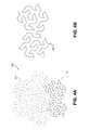
- FIG. 3Ais a diagram illustrating a 7-segment fractal curve that forms an originator stage of the Peano-Gosper fractal.
- FIG. 3Bis a diagram illustrating a 49-segment fractal curve that forms the second stage of the Peano-Gosper fractal.
- FIG. 3Cis a diagram illustrating a 343-segment fractal curve that forms the third stage of the Peano-Gosper fractal.
- FIG. 3Dis a diagram illustrating a 2401-segment fractal curve that forms the fourth stage of the Peano-Gosper fractal.
- FIG. 4Ais a diagram showing a 100-segment portion of the 343-segment Peano-Gosper fractal curve of FIG. 3C that is used to form a fractal antenna for one embodiment of the present invention.
- FIG. 4Bshows the 100-segment fractal of FIG. 4A .
- FIG. 5shows the implementation of the 100-segment fractal of FIG. 4B to construct a modified Peano-Gosper fractal antenna array, in which the particular embodiment shown implements rounded corners to remove sharp discontinuities at segment joints.
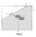
- FIG. 6is a diagram illustrating a placement of a 100-segment fractal antenna array of FIG. 5 on a dielectric substrate to form a monopole antenna.
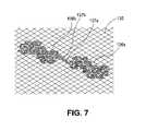
- FIG. 7is a diagram illustrating a placement of two 100-segment fractal antenna array of FIG. 5 on a dielectric substrate to form a dipole antenna.
- the embodiments of the present inventionmay be practiced in a variety of settings that implement a fractal antenna and, particularly to fractal antenna arrays based on a modified Peano-Gosper curve.
- FIG. 1is a schematic block diagram illustrating a communication system 10 that includes a plurality of base stations and/or access points (BS/AP) 15 , 16 , 17 , a plurality of wireless communication devices 20 - 28 and a network hardware component 30 .
- Network hardware component 30which may be a router, switch, bridge, modem, system controller, et cetera, may provide a wide area network (WAN) coupling 31 for communication system 10 .
- wireless communication devices 20 - 28may be of a variety of devices, including laptop computers 21 , 25 ; personal digital assistants (PDA) 20 , 27 ; personal computers (PC) 23 , 24 , 28 ; and/or cellular telephones (cell phone) 22 , 26 . The details of the wireless communication devices shown is described in greater detail with reference to FIG. 2 .
- Wireless communication devices 22 , 23 , and 24are shown located within an independent basic service set (IBSS) area 13 and these devices communicate directly (i.e., point to point). In this example configuration, these devices 22 , 23 , and 24 typically communicate only with each other. To communicate with other wireless communication devices within system 10 or to communicate outside of system 10 , devices 22 - 24 may affiliate with a base station or access point, such as BS/AP 17 , or one of the other BS/AP units 15 , 16 .
- IBSSindependent basic service set
- BS/AP 15 , 16are typically located within respective basic service set (BSS) areas 11 , 12 and are directly or indirectly coupled to network hardware component 30 via local area network (LAN) couplings 32 , 33 . Such couplings provide BS/AP 15 , 16 with connectivity to other devices within system 10 and provide connectivity to other networks via WAN connection 31 .
- BSSbasic service set
- LANlocal area network
- each of the BS/AP 15 , 16has an associated antenna or antenna array. For instance, BS/AP 15 wirelessly communicates with wireless communication devices 20 , 21 , while BS/AP 16 wirelessly communicates with wireless communication devices 25 - 28 .
- the wireless communication devicesregister with a particular BS/AP 15 , 16 to receive services within communication system 10 .
- LAN coupling 17may couple BS/AP 17 to network hardware component 30 .
- each wireless communication deviceincludes a built-in radio and/or is coupled to a radio.
- FIG. 2is a schematic block diagram illustrating a wireless communication device that includes a host 40 and an associated radio 60 .
- Host 40may be one of the devices 20 - 28 shown in FIG. 1 .
- radio 60is typically a built-in component.
- radio 60may be built-in or an externally coupled component.
- host 40includes a processing module 50 , memory 52 , radio interface 54 , input interface 58 and output interface 56 .
- Processing module 50 and memory 52execute corresponding instructions that are typically done by the host device. For example, for a cellular telephone host device, processing module 50 may perform the corresponding communication functions in accordance with a particular cellular telephone standard.
- radio interface 54allows data to be received from and sent to radio 60 .
- radio interface 54For data received from radio 60 (such as inbound data 92 ), radio interface 54 provides the data to processing module 50 for further processing and/or routing to output interface 56 .
- Output interface 56provides connectivity on line 57 to an output device, such as a display, monitor, speakers, et cetera, in order to output the received data.
- Radio interface 54also provides data from processing module 50 to radio 60 .
- Processing module 50may receive outbound data on line 59 from an input device, such as a keyboard, keypad, microphone, et cetera, via input interface 58 or generate the data itself.
- processing module 50may perform a corresponding host function on the data and/or route it to radio 60 via radio interface 54 .
- Radio 60includes a host interface 62 , a baseband processing module 63 , memory 65 , one or more radio frequency (RF) transmitter units 70 , a transmit/receive (T/R) module 80 , one or more antennas 81 , one or more RF receivers 71 and a local oscillation (LO) module 64 .
- Baseband processing module 63in combination with operational instructions stored in memory 65 , executes digital receiver functions and digital transmitter functions.
- the digital receiver functionsinclude, but are not limited to, digital intermediate frequency to baseband conversion, demodulation, constellation demapping, decoding, de-interleaving, fast Fourier transform, cyclic prefix removal, space and time decoding, and/or descrambling.
- the digital transmitter functionsinclude, but are not limited to, scrambling, encoding, interleaving, constellation mapping, modulation, inverse fast Fourier transform, cyclic prefix addition, space and time encoding, and digital baseband to IF conversion.
- Baseband processing module 63may be implemented using one or more processing devices.
- processing device(s)may be a microprocessor, micro-controller, digital signal processor, microcomputer, central processing unit, field programmable gate array, programmable logic device, state machine, logic circuitry, analog circuitry, digital circuitry, and/or any device that manipulates signals (analog and/or digital) based on operational instructions.
- Memory 65may be a single memory device or a plurality of memory devices. Such a memory device may be a read-only memory, random access memory, volatile memory, non-volatile memory, static memory, dynamic memory, flash memory, and/or any device that stores digital information. Note that when processing module 63 implements one or more of its functions via a state machine, analog circuitry, digital circuitry, and/or logic circuitry, the memory storing the corresponding operational instructions may be embedded with the circuitry comprising the state machine, analog circuitry, digital circuitry, and/or logic circuitry.
- radio 60receives outbound data 93 from host 40 via host interface 62 .
- Baseband processing module 63receives outbound data 93 and based on a mode selection signal 91 , produces one or more outbound symbol streams 95 .
- Mode selection signal 91typically indicates a particular mode of operation that is compliant with one or more specific modes of the various IEEE 802.11 standards.
- mode selection signal 91may indicate a frequency band of 2.4 GHz, a channel bandwidth of 20 or 22 MHz and a maximum bit rate of 54 megabits-per-second.
- mode selection signal 91may further indicate a particular rate ranging from 1 megabit-per-second to 54 megabits-per-second, or higher.
- mode selection signal 91may indicate a particular type of modulation, which includes, but is not limited to, Barker Code Modulation, BPSK, QPSK, CCK, 16 QAM and/or 64 QAM, as well as others. Mode selection signal 91 may also include a code rate, a number of coded bits per subcarrier (NBPSC), coded bits per OFDM symbol (NCBPS), and/or data bits per OFDM symbol (NDBPS). Mode selection signal 91 may also indicate a particular channelization for the corresponding mode that provides a channel number and corresponding center frequency. Mode select signal 91 may further indicate a power spectral density mask value and a number of antennas to be initially used for a MIMO communication.
- Baseband processing module 63based on mode selection signal 91 , produces one or more outbound symbol streams 95 from outbound data 93 . For example, if mode selection signal 91 indicates that a single transmit antenna is being utilized for the particular mode that has been selected, baseband processing module 63 produces a single outbound symbol stream 95 . Alternatively, if mode selection signal 91 indicates 2, 3 or 4 antennas, baseband processing module 63 produces respective 2, 3 or 4 outbound symbol streams 95 from outbound data 93 .
- each RF transmitter 70includes a digital filter and up sampling module, a digital to analog conversion module, an analog filter module, a frequency up conversion module, a power amplifier, and a radio frequency bandpass filter.
- RF transmitters 70provide outbound RF signals 97 to T/R module 80 , which provides each outbound RF signal 97 to a corresponding antenna 81 .
- T/R module 80receives one or more inbound RF signals 96 via antenna(s) 81 and provides signal(s) 96 to respective one or more RF receivers 71 .
- RF receiver(s) 71converts inbound RF signals 96 into a corresponding number of inbound symbol streams 94 .
- the number of inbound symbol streams 94corresponds to the particular mode in which the data was received.
- Baseband processing module 63converts inbound symbol streams 94 into inbound data 92 , which is provided to host 40 via host interface 62 .
- the wireless communication device of FIG. 2may be implemented using one or more integrated circuits.
- host 40may be implemented on one integrated circuit
- baseband processing module 63 and memory 65may be implemented on a second integrated circuit
- the remaining components of radio 60(less the antennas 81 ) may be implemented on a third integrated circuit.
- baseband processing module 63 and radio 60may be implemented on a single integrated circuit.
- processing module 50 of host 40 and baseband processing module 63may be a common processing device implemented on a single integrated circuit.
- memory 52 and memory 65may be implemented on the same memory device and/or on the same integrated circuit as the common processing modules of processing module 50 and baseband processing module 63 . It is be noted that other embodiments may be implemented with the various units of FIG. 2 .
- the various embodiments of the wireless communication device of FIG. 2may be implemented in a transmitter and/or a receiver utilized for wireless communications. Typically, the communication is both ways so that the two units communicating typically will employ a transceiver in order to send and receive data.
- the multiple RF transmitters 70 and RF receivers 71allow the device of FIG. 2 to be utilized in a multiple antenna transceiver system.
- FIG. 3shows one particular example when communication is achieved using two antennas at the transmitter and two antennas at the receiver.
- antenna 81In reference to antenna 81 (or antennas, depending on how many are present), it may be externally disposed to radio 60 or provided as part of an integrated circuit that comprises radio 60 . Although a variety of antennas may be implemented for antenna 81 , in one scheme, a fractal antenna is used. For example, a fractal antenna may be constructed within the integrated circuit comprising radio 60 or, alternatively, the fractal antenna may be constructed externally, such as on a circuit board (or other substrate) that also holds radio 60 . In one embodiment, a fractal antenna based on a modified Peano-Gosper curve, as described below, may be employed for antenna 81 .
- FIG. 3Ashows a particular fractal 100 which has a curve shape that is referred to as a Peano-Gosper (P-G) curve.
- Fractal 100is comprised of seven segments labeled a-g. The seven segments (7 1 ) have equal length and form the first stage (originator stage) of the P-G curve. Note that the long length portion of the P-G fractal 100 is actually formed by two segments b and c. This originator fractal 100 is then utilized to generate subsequent stages of the P-G geometry as recursions are employed to expand the P-G curve.
- FIG. 3Bshows a first recursion of the P-G curve subsequent to the originator fractal 100 shown in FIG. 3A .
- First recursion (second stage) of the P-G curveis shown as fractal array 101 .
- fractal array 101has 49 (7 2 ) segments formed by seven 7-segment fractals.
- fractal array 101has one 7-segment fractal in the center, circumscribed by the remaining six 7-segment fractals.
- a subsequent second recursion (third stage) of the P-G curveis shown as fractal array 102 in FIG. 3C .
- fractal 102has 343 (7 3 ) segments formed by seven 49-segment fractals, in which six 49-segment fractals 101 circumscribe the one 49-segment fractal in the center.
- FIG. 3Dshows a third recursion (fourth stage) of the P-G curve in fractal array 103 .
- Fractal array 103has 2401 (7 4 ) segments formed by seven 343-segment fractals, in which six 343-segment fractals 102 circumscribe the one 343-segment fractal in the center.
- the next recursion(not shown) would be a fractal array comprised of seven 2401-segment fractals 103 , in which six such fractals 103 would circumscribe the center fractal.
- the processmay be repeated infinitely in a similar manner for subsequent recursions.
- each recursion growth of the P-G curveresults in a previous fractal array being duplicated in a similar geometric pattern, having one fractal array in the center circumscribed by six other identical fractal arrays.
- the growth in all instancesis outwardly from the center in a substantially omni-directional expansion of the geometric P-G pattern.
- the resulting antennaemploys one of the patterns shown in FIGS. 3A-3D , or one of the subsequent recursion.
- FIG. 4A-4Billustrate a fractal design utilizing a modified P-G curve.
- one embodiment for constructing a fractal antennautilizes this modified P-G curve.
- FIG. 4Aa 343-segment fractal array 102 of FIG. 3C is shown again. However, instead of using all 343 segments, only 100 segments out of the total 343 segments are utilized.
- the 100-segment fractal 110is shown in solid lines and the remaining unused portion 111 is shown in dotted lines in FIG. 4A .
- Fractal 110is shown enlarged in FIG. 4B .
- the 100-segment fractal design of fractal 110is obtained from two of the adjacent border 49-segment fractals plus 2 additional segments.
- the dimensionsare such that fractal 110 has a cross-section that is longer in length than its width, which is unlike the circular cross-section of the standard P-G curve.
- a fractal antennais constructed using this 100-segment portion of the P-G curve.
- FIG. 5shows one embodiment of a fractal antenna array 120 constructed using the 100-segment modified P-G curve of FIG. 4B .
- dimension of length Lis longer than the dimension of width W.
- a conductive lead 121is also shown to couple the fractal antenna array 120 to RF components and/or circuitry.
- the embodiment of FIG. 5shows an implementation in which corners where the segments join are rounded to remove the sharp discontinuity. It is to be noted that other embodiments may use the specific design of FIG. 4B , in which the segment corners are not rounded.
- the fractal antenna array 120may be implemented in a variety of ways to perform as an antenna.
- the antenna array 120may be implemented in the integrated circuit itself with the RF circuitry; implemented separately from the integrated circuit, but in the same module or package; implemented on a substrate or circuit board on which the RF circuitry is resident; or implemented as a completely separate antenna.
- FIG. 6shows antenna 120 , with lead 121 , implemented on a printed circuit board (PCB) 130 , in which lead 121 is used to couple antenna 120 to integrated circuit 131 , which is also disposed on PCB 130 .
- PCBprinted circuit board
- a 100-segment modified fractal antenna array made from a copper materialhas dimensions of approximately 349 mils for length L and 208 mils for width W. This antenna is then disposed on a PCB made from a FR4 dielectric to operate at or near a frequency of approximately 2.4 GHz.
- FIG. 6shows a monopole antenna design.
- a dipole antenna designmay be desired.
- FIG. 7illustrates the use of two 100-segment P-G curve fractal antennas to form a dipole antenna.
- a pair of 100-segment P-G curve fractal antenna arrays 136 a - 136 bwith corresponding leads 137 a - 137 b , are formed on a substrate or PCB 135 . Leads 137 a - 137 b would then be coupled to appropriate circuitry.
- the design of the fractal antenna array using the modified 100-segment P-G curveallows for an antenna that has a length dimension L that is longer than the width dimension W (shown in FIG. 5 ).
- the antenna constructionis obtained from uniform expansion of the fractal, and in which the uniform radiation pattern may lead to cancellation effects in the radiated electromagnetic field.
- the 100-segment modified designhas growth in a linear direction, so that the field cancellation effects are reduced.
- antenna efficiencyis the ratio of radiated power to accepted power for the antenna.
- Performance indicatorshave shown that significant antenna power efficiency may be obtained with the use of a fractal antenna using a modified P-G curve, in which the modified design has a non-uniform fractal growth, such as expanding more in one linear direction (L) versus a corresponding perpendicular direction (W). Additionally, the fractal design may implement rounded corners, which may aid in reducing sharp changes or discontinuities of the radiated electromagnetic field.
- the fractal design described aboveuses a modified 100-segment P-G curve.
- the antenna designneed not be limited to a 100-segment design or an approximate 100-segment curve (e.g. 100 ⁇ n). It may be constructed from a P-G curve of higher (or lower) recursion.
- the antennaneed not be limited to the use of a Peano-Gosper curve. Other embodiments may use other types of fractal curves.
- the modified curveis selected to have more fractal expansion in a linear direction so that the L and W dimensions are substantially different.
- the actual curve used and the number of segments selectedmay be dependent on the particular use of the antenna, frequency of operation and/or the radiation pattern desired. Additionally, the actual dimensions of the antenna, whether the 100 segment P-G curve or some other design, the dimensions of the antenna may be changed to obtained various electrical properties, including frequency of operation for the antenna.
- a fractal antenna using a modified fractal curvesuch as a modified P-G curve
- the antennais constructed from materials that are used for typical antenna construction.
- the conductoris copper.
- the antennais formed on a non-conductor, such as a dielectric material.
- the antennamay be employed in various devices, including wireless devices.
- the fractal antennais used for one or more antennas 81 , shown in FIG. 2 , which may be incorporated on one or more wireless devices, such as those wireless devices shown in FIG. 1 .
- Embodiments of the described fractal antennaneed not be limited to the circuitry of FIG. 2 or devices shown in FIG. 1 .
- the terms “substantially” and “approximately”provides an industry-accepted tolerance for its corresponding term and/or relativity between items. Such an industry-accepted tolerance ranges from less than one percent to fifty percent and corresponds to, but is not limited to, component values, integrated circuit process variations, temperature variations, rise and fall times, and/or thermal noise. Such relativity between items ranges from a difference of a few percent to magnitude differences.
- the term(s) “coupled” and/or “coupling”includes direct coupling between items and/or indirect coupling between items via an intervening item (e.g., an item includes, but is not limited to, a component, an element, a circuit, and/or a module) where, for indirect coupling, the intervening item does not modify the information of a signal but may adjust its current level, voltage level, and/or power level.
- an intervening iteme.g., an item includes, but is not limited to, a component, an element, a circuit, and/or a module
- inferred couplingi.e., where one element is coupled to another element by inference
- inferred couplingincludes direct and indirect coupling between two items in the same manner as “coupled to”.
- the term “operable to”indicates that an item includes one or more of power connections, input(s), output(s), etc., to perform one or more of its corresponding functions and may further include inferred coupling to one or more other items.
- moduleis used herein to describe a functional block and may represent hardware, software, firmware, etc., without limitation to its structure.
- a “module”may be a circuit, integrated circuit chip or chips, assembly or other component configurations.
- a “processing module”may be a single processing device or a plurality of processing devices.
- Such a processing devicemay be a microprocessor, micro-controller, digital signal processor, microcomputer, central processing unit, field programmable gate array, programmable logic device, state machine, logic circuitry, analog circuitry, digital circuitry, and/or any device that manipulates signals (analog and/or digital) based on hard coding of the circuitry and/or operational instructions and such processing device may have accompanying memory.
- a “module”may also be software or software operating in conjunction with hardware.
Landscapes
- Engineering & Computer Science (AREA)
- Computer Networks & Wireless Communication (AREA)
- Radio Transmission System (AREA)
- Support Of Aerials (AREA)
Abstract
Description
Claims (20)
Priority Applications (1)
| Application Number | Priority Date | Filing Date | Title |
|---|---|---|---|
| US11/648,448US7541981B2 (en) | 2006-10-04 | 2006-12-28 | Fractal antenna based on Peano-Gosper curve |
Applications Claiming Priority (2)
| Application Number | Priority Date | Filing Date | Title |
|---|---|---|---|
| US84926906P | 2006-10-04 | 2006-10-04 | |
| US11/648,448US7541981B2 (en) | 2006-10-04 | 2006-12-28 | Fractal antenna based on Peano-Gosper curve |
Publications (2)
| Publication Number | Publication Date |
|---|---|
| US20080084352A1 US20080084352A1 (en) | 2008-04-10 |
| US7541981B2true US7541981B2 (en) | 2009-06-02 |
Family
ID=39274580
Family Applications (1)
| Application Number | Title | Priority Date | Filing Date |
|---|---|---|---|
| US11/648,448Expired - Fee RelatedUS7541981B2 (en) | 2006-10-04 | 2006-12-28 | Fractal antenna based on Peano-Gosper curve |
Country Status (1)
| Country | Link |
|---|---|
| US (1) | US7541981B2 (en) |
Cited By (142)
| Publication number | Priority date | Publication date | Assignee | Title |
|---|---|---|---|---|
| US20100103052A1 (en)* | 2008-10-23 | 2010-04-29 | Sony Ericsson Mobile Communications Ab | Antenna assembly |
| US20110254739A1 (en)* | 2010-04-16 | 2011-10-20 | U. S. A. As Represented By The Administrator Of The National Aeronautics And Space Administration | Antenna with Dielectric Having Geometric Patterns |
| US9608740B2 (en) | 2015-07-15 | 2017-03-28 | At&T Intellectual Property I, L.P. | Method and apparatus for launching a wave mode that mitigates interference |
| US9640850B2 (en) | 2015-06-25 | 2017-05-02 | At&T Intellectual Property I, L.P. | Methods and apparatus for inducing a non-fundamental wave mode on a transmission medium |
| US9667317B2 (en) | 2015-06-15 | 2017-05-30 | At&T Intellectual Property I, L.P. | Method and apparatus for providing security using network traffic adjustments |
| US9674711B2 (en) | 2013-11-06 | 2017-06-06 | At&T Intellectual Property I, L.P. | Surface-wave communications and methods thereof |
| US9685992B2 (en) | 2014-10-03 | 2017-06-20 | At&T Intellectual Property I, L.P. | Circuit panel network and methods thereof |
| US9705561B2 (en) | 2015-04-24 | 2017-07-11 | At&T Intellectual Property I, L.P. | Directional coupling device and methods for use therewith |
| US9705610B2 (en) | 2014-10-21 | 2017-07-11 | At&T Intellectual Property I, L.P. | Transmission device with impairment compensation and methods for use therewith |
| US9722318B2 (en) | 2015-07-14 | 2017-08-01 | At&T Intellectual Property I, L.P. | Method and apparatus for coupling an antenna to a device |
| US9729197B2 (en) | 2015-10-01 | 2017-08-08 | At&T Intellectual Property I, L.P. | Method and apparatus for communicating network management traffic over a network |
| US9735833B2 (en) | 2015-07-31 | 2017-08-15 | At&T Intellectual Property I, L.P. | Method and apparatus for communications management in a neighborhood network |
| US9742521B2 (en) | 2014-11-20 | 2017-08-22 | At&T Intellectual Property I, L.P. | Transmission device with mode division multiplexing and methods for use therewith |
| US9742462B2 (en) | 2014-12-04 | 2017-08-22 | At&T Intellectual Property I, L.P. | Transmission medium and communication interfaces and methods for use therewith |
| US9749013B2 (en) | 2015-03-17 | 2017-08-29 | At&T Intellectual Property I, L.P. | Method and apparatus for reducing attenuation of electromagnetic waves guided by a transmission medium |
| US9749053B2 (en) | 2015-07-23 | 2017-08-29 | At&T Intellectual Property I, L.P. | Node device, repeater and methods for use therewith |
| US9748626B2 (en) | 2015-05-14 | 2017-08-29 | At&T Intellectual Property I, L.P. | Plurality of cables having different cross-sectional shapes which are bundled together to form a transmission medium |
| US9762289B2 (en) | 2014-10-14 | 2017-09-12 | At&T Intellectual Property I, L.P. | Method and apparatus for transmitting or receiving signals in a transportation system |
| US9769020B2 (en) | 2014-10-21 | 2017-09-19 | At&T Intellectual Property I, L.P. | Method and apparatus for responding to events affecting communications in a communication network |
| US9768833B2 (en) | 2014-09-15 | 2017-09-19 | At&T Intellectual Property I, L.P. | Method and apparatus for sensing a condition in a transmission medium of electromagnetic waves |
| US9769128B2 (en) | 2015-09-28 | 2017-09-19 | At&T Intellectual Property I, L.P. | Method and apparatus for encryption of communications over a network |
| US9780834B2 (en) | 2014-10-21 | 2017-10-03 | At&T Intellectual Property I, L.P. | Method and apparatus for transmitting electromagnetic waves |
| US9788326B2 (en) | 2012-12-05 | 2017-10-10 | At&T Intellectual Property I, L.P. | Backhaul link for distributed antenna system |
| US9787412B2 (en) | 2015-06-25 | 2017-10-10 | At&T Intellectual Property I, L.P. | Methods and apparatus for inducing a fundamental wave mode on a transmission medium |
| US9793951B2 (en) | 2015-07-15 | 2017-10-17 | At&T Intellectual Property I, L.P. | Method and apparatus for launching a wave mode that mitigates interference |
| US9793955B2 (en) | 2015-04-24 | 2017-10-17 | At&T Intellectual Property I, Lp | Passive electrical coupling device and methods for use therewith |
| US9793954B2 (en) | 2015-04-28 | 2017-10-17 | At&T Intellectual Property I, L.P. | Magnetic coupling device and methods for use therewith |
| US9800327B2 (en) | 2014-11-20 | 2017-10-24 | At&T Intellectual Property I, L.P. | Apparatus for controlling operations of a communication device and methods thereof |
| US9820146B2 (en) | 2015-06-12 | 2017-11-14 | At&T Intellectual Property I, L.P. | Method and apparatus for authentication and identity management of communicating devices |
| US9838896B1 (en) | 2016-12-09 | 2017-12-05 | At&T Intellectual Property I, L.P. | Method and apparatus for assessing network coverage |
| US9838078B2 (en) | 2015-07-31 | 2017-12-05 | At&T Intellectual Property I, L.P. | Method and apparatus for exchanging communication signals |
| US9847850B2 (en) | 2014-10-14 | 2017-12-19 | At&T Intellectual Property I, L.P. | Method and apparatus for adjusting a mode of communication in a communication network |
| US9847566B2 (en) | 2015-07-14 | 2017-12-19 | At&T Intellectual Property I, L.P. | Method and apparatus for adjusting a field of a signal to mitigate interference |
| US9853342B2 (en) | 2015-07-14 | 2017-12-26 | At&T Intellectual Property I, L.P. | Dielectric transmission medium connector and methods for use therewith |
| US9860075B1 (en) | 2016-08-26 | 2018-01-02 | At&T Intellectual Property I, L.P. | Method and communication node for broadband distribution |
| US9866309B2 (en) | 2015-06-03 | 2018-01-09 | At&T Intellectual Property I, Lp | Host node device and methods for use therewith |
| US9865911B2 (en) | 2015-06-25 | 2018-01-09 | At&T Intellectual Property I, L.P. | Waveguide system for slot radiating first electromagnetic waves that are combined into a non-fundamental wave mode second electromagnetic wave on a transmission medium |
| US9866276B2 (en) | 2014-10-10 | 2018-01-09 | At&T Intellectual Property I, L.P. | Method and apparatus for arranging communication sessions in a communication system |
| US9871283B2 (en) | 2015-07-23 | 2018-01-16 | At&T Intellectual Property I, Lp | Transmission medium having a dielectric core comprised of plural members connected by a ball and socket configuration |
| US9871558B2 (en) | 2014-10-21 | 2018-01-16 | At&T Intellectual Property I, L.P. | Guided-wave transmission device and methods for use therewith |
| US9871282B2 (en) | 2015-05-14 | 2018-01-16 | At&T Intellectual Property I, L.P. | At least one transmission medium having a dielectric surface that is covered at least in part by a second dielectric |
| US9876605B1 (en) | 2016-10-21 | 2018-01-23 | At&T Intellectual Property I, L.P. | Launcher and coupling system to support desired guided wave mode |
| US9876571B2 (en) | 2015-02-20 | 2018-01-23 | At&T Intellectual Property I, Lp | Guided-wave transmission device with non-fundamental mode propagation and methods for use therewith |
| US9876264B2 (en) | 2015-10-02 | 2018-01-23 | At&T Intellectual Property I, Lp | Communication system, guided wave switch and methods for use therewith |
| US9882257B2 (en) | 2015-07-14 | 2018-01-30 | At&T Intellectual Property I, L.P. | Method and apparatus for launching a wave mode that mitigates interference |
| US9887447B2 (en) | 2015-05-14 | 2018-02-06 | At&T Intellectual Property I, L.P. | Transmission medium having multiple cores and methods for use therewith |
| US9893795B1 (en) | 2016-12-07 | 2018-02-13 | At&T Intellectual Property I, Lp | Method and repeater for broadband distribution |
| US9906269B2 (en) | 2014-09-17 | 2018-02-27 | At&T Intellectual Property I, L.P. | Monitoring and mitigating conditions in a communication network |
| US9913139B2 (en) | 2015-06-09 | 2018-03-06 | At&T Intellectual Property I, L.P. | Signal fingerprinting for authentication of communicating devices |
| US9912382B2 (en) | 2015-06-03 | 2018-03-06 | At&T Intellectual Property I, Lp | Network termination and methods for use therewith |
| US9912033B2 (en) | 2014-10-21 | 2018-03-06 | At&T Intellectual Property I, Lp | Guided wave coupler, coupling module and methods for use therewith |
| US9912027B2 (en) | 2015-07-23 | 2018-03-06 | At&T Intellectual Property I, L.P. | Method and apparatus for exchanging communication signals |
| US9912419B1 (en) | 2016-08-24 | 2018-03-06 | At&T Intellectual Property I, L.P. | Method and apparatus for managing a fault in a distributed antenna system |
| US9911020B1 (en) | 2016-12-08 | 2018-03-06 | At&T Intellectual Property I, L.P. | Method and apparatus for tracking via a radio frequency identification device |
| US9917341B2 (en) | 2015-05-27 | 2018-03-13 | At&T Intellectual Property I, L.P. | Apparatus and method for launching electromagnetic waves and for modifying radial dimensions of the propagating electromagnetic waves |
| US9927517B1 (en) | 2016-12-06 | 2018-03-27 | At&T Intellectual Property I, L.P. | Apparatus and methods for sensing rainfall |
| US9930668B2 (en) | 2013-05-31 | 2018-03-27 | At&T Intellectual Property I, L.P. | Remote distributed antenna system |
| US9929755B2 (en) | 2015-07-14 | 2018-03-27 | At&T Intellectual Property I, L.P. | Method and apparatus for coupling an antenna to a device |
| US9948333B2 (en) | 2015-07-23 | 2018-04-17 | At&T Intellectual Property I, L.P. | Method and apparatus for wireless communications to mitigate interference |
| US9948354B2 (en) | 2015-04-28 | 2018-04-17 | At&T Intellectual Property I, L.P. | Magnetic coupling device with reflective plate and methods for use therewith |
| US9948355B2 (en) | 2014-10-21 | 2018-04-17 | At&T Intellectual Property I, L.P. | Apparatus for providing communication services and methods thereof |
| US9954286B2 (en) | 2014-10-21 | 2018-04-24 | At&T Intellectual Property I, L.P. | Guided-wave transmission device with non-fundamental mode propagation and methods for use therewith |
| US9954287B2 (en) | 2014-11-20 | 2018-04-24 | At&T Intellectual Property I, L.P. | Apparatus for converting wireless signals and electromagnetic waves and methods thereof |
| US9967173B2 (en) | 2015-07-31 | 2018-05-08 | At&T Intellectual Property I, L.P. | Method and apparatus for authentication and identity management of communicating devices |
| US9973940B1 (en) | 2017-02-27 | 2018-05-15 | At&T Intellectual Property I, L.P. | Apparatus and methods for dynamic impedance matching of a guided wave launcher |
| US9973416B2 (en) | 2014-10-02 | 2018-05-15 | At&T Intellectual Property I, L.P. | Method and apparatus that provides fault tolerance in a communication network |
| US9991580B2 (en) | 2016-10-21 | 2018-06-05 | At&T Intellectual Property I, L.P. | Launcher and coupling system for guided wave mode cancellation |
| US9997819B2 (en) | 2015-06-09 | 2018-06-12 | At&T Intellectual Property I, L.P. | Transmission medium and method for facilitating propagation of electromagnetic waves via a core |
| US9999038B2 (en) | 2013-05-31 | 2018-06-12 | At&T Intellectual Property I, L.P. | Remote distributed antenna system |
| US9998870B1 (en) | 2016-12-08 | 2018-06-12 | At&T Intellectual Property I, L.P. | Method and apparatus for proximity sensing |
| US10009063B2 (en) | 2015-09-16 | 2018-06-26 | At&T Intellectual Property I, L.P. | Method and apparatus for use with a radio distributed antenna system having an out-of-band reference signal |
| US10009067B2 (en) | 2014-12-04 | 2018-06-26 | At&T Intellectual Property I, L.P. | Method and apparatus for configuring a communication interface |
| US10020844B2 (en) | 2016-12-06 | 2018-07-10 | T&T Intellectual Property I, L.P. | Method and apparatus for broadcast communication via guided waves |
| US10027397B2 (en) | 2016-12-07 | 2018-07-17 | At&T Intellectual Property I, L.P. | Distributed antenna system and methods for use therewith |
| US10027398B2 (en) | 2015-06-11 | 2018-07-17 | At&T Intellectual Property I, Lp | Repeater and methods for use therewith |
| US10033108B2 (en) | 2015-07-14 | 2018-07-24 | At&T Intellectual Property I, L.P. | Apparatus and methods for generating an electromagnetic wave having a wave mode that mitigates interference |
| US10044409B2 (en) | 2015-07-14 | 2018-08-07 | At&T Intellectual Property I, L.P. | Transmission medium and methods for use therewith |
| US10069535B2 (en) | 2016-12-08 | 2018-09-04 | At&T Intellectual Property I, L.P. | Apparatus and methods for launching electromagnetic waves having a certain electric field structure |
| US10079661B2 (en) | 2015-09-16 | 2018-09-18 | At&T Intellectual Property I, L.P. | Method and apparatus for use with a radio distributed antenna system having a clock reference |
| US10090606B2 (en) | 2015-07-15 | 2018-10-02 | At&T Intellectual Property I, L.P. | Antenna system with dielectric array and methods for use therewith |
| US10090594B2 (en) | 2016-11-23 | 2018-10-02 | At&T Intellectual Property I, L.P. | Antenna system having structural configurations for assembly |
| US10103422B2 (en) | 2016-12-08 | 2018-10-16 | At&T Intellectual Property I, L.P. | Method and apparatus for mounting network devices |
| US10103801B2 (en) | 2015-06-03 | 2018-10-16 | At&T Intellectual Property I, L.P. | Host node device and methods for use therewith |
| US10135147B2 (en) | 2016-10-18 | 2018-11-20 | At&T Intellectual Property I, L.P. | Apparatus and methods for launching guided waves via an antenna |
| US10135145B2 (en) | 2016-12-06 | 2018-11-20 | At&T Intellectual Property I, L.P. | Apparatus and methods for generating an electromagnetic wave along a transmission medium |
| US10135146B2 (en) | 2016-10-18 | 2018-11-20 | At&T Intellectual Property I, L.P. | Apparatus and methods for launching guided waves via circuits |
| US10136434B2 (en) | 2015-09-16 | 2018-11-20 | At&T Intellectual Property I, L.P. | Method and apparatus for use with a radio distributed antenna system having an ultra-wideband control channel |
| US10139820B2 (en) | 2016-12-07 | 2018-11-27 | At&T Intellectual Property I, L.P. | Method and apparatus for deploying equipment of a communication system |
| US10148016B2 (en) | 2015-07-14 | 2018-12-04 | At&T Intellectual Property I, L.P. | Apparatus and methods for communicating utilizing an antenna array |
| US10144036B2 (en) | 2015-01-30 | 2018-12-04 | At&T Intellectual Property I, L.P. | Method and apparatus for mitigating interference affecting a propagation of electromagnetic waves guided by a transmission medium |
| US10168695B2 (en) | 2016-12-07 | 2019-01-01 | At&T Intellectual Property I, L.P. | Method and apparatus for controlling an unmanned aircraft |
| US10170840B2 (en) | 2015-07-14 | 2019-01-01 | At&T Intellectual Property I, L.P. | Apparatus and methods for sending or receiving electromagnetic signals |
| US10178445B2 (en) | 2016-11-23 | 2019-01-08 | At&T Intellectual Property I, L.P. | Methods, devices, and systems for load balancing between a plurality of waveguides |
| US10205655B2 (en) | 2015-07-14 | 2019-02-12 | At&T Intellectual Property I, L.P. | Apparatus and methods for communicating utilizing an antenna array and multiple communication paths |
| US10225025B2 (en) | 2016-11-03 | 2019-03-05 | At&T Intellectual Property I, L.P. | Method and apparatus for detecting a fault in a communication system |
| US10224634B2 (en) | 2016-11-03 | 2019-03-05 | At&T Intellectual Property I, L.P. | Methods and apparatus for adjusting an operational characteristic of an antenna |
| US10243784B2 (en) | 2014-11-20 | 2019-03-26 | At&T Intellectual Property I, L.P. | System for generating topology information and methods thereof |
| US10243270B2 (en) | 2016-12-07 | 2019-03-26 | At&T Intellectual Property I, L.P. | Beam adaptive multi-feed dielectric antenna system and methods for use therewith |
| US10264586B2 (en) | 2016-12-09 | 2019-04-16 | At&T Mobility Ii Llc | Cloud-based packet controller and methods for use therewith |
| US10291311B2 (en) | 2016-09-09 | 2019-05-14 | At&T Intellectual Property I, L.P. | Method and apparatus for mitigating a fault in a distributed antenna system |
| US10291334B2 (en) | 2016-11-03 | 2019-05-14 | At&T Intellectual Property I, L.P. | System for detecting a fault in a communication system |
| US10298293B2 (en) | 2017-03-13 | 2019-05-21 | At&T Intellectual Property I, L.P. | Apparatus of communication utilizing wireless network devices |
| US10305190B2 (en) | 2016-12-01 | 2019-05-28 | At&T Intellectual Property I, L.P. | Reflecting dielectric antenna system and methods for use therewith |
| US10312567B2 (en) | 2016-10-26 | 2019-06-04 | At&T Intellectual Property I, L.P. | Launcher with planar strip antenna and methods for use therewith |
| US10320586B2 (en) | 2015-07-14 | 2019-06-11 | At&T Intellectual Property I, L.P. | Apparatus and methods for generating non-interfering electromagnetic waves on an insulated transmission medium |
| US10326494B2 (en) | 2016-12-06 | 2019-06-18 | At&T Intellectual Property I, L.P. | Apparatus for measurement de-embedding and methods for use therewith |
| US10326689B2 (en) | 2016-12-08 | 2019-06-18 | At&T Intellectual Property I, L.P. | Method and system for providing alternative communication paths |
| US10340601B2 (en) | 2016-11-23 | 2019-07-02 | At&T Intellectual Property I, L.P. | Multi-antenna system and methods for use therewith |
| US10340983B2 (en) | 2016-12-09 | 2019-07-02 | At&T Intellectual Property I, L.P. | Method and apparatus for surveying remote sites via guided wave communications |
| US10340573B2 (en) | 2016-10-26 | 2019-07-02 | At&T Intellectual Property I, L.P. | Launcher with cylindrical coupling device and methods for use therewith |
| US10340600B2 (en) | 2016-10-18 | 2019-07-02 | At&T Intellectual Property I, L.P. | Apparatus and methods for launching guided waves via plural waveguide systems |
| US10341142B2 (en) | 2015-07-14 | 2019-07-02 | At&T Intellectual Property I, L.P. | Apparatus and methods for generating non-interfering electromagnetic waves on an uninsulated conductor |
| US10340603B2 (en) | 2016-11-23 | 2019-07-02 | At&T Intellectual Property I, L.P. | Antenna system having shielded structural configurations for assembly |
| US10355367B2 (en) | 2015-10-16 | 2019-07-16 | At&T Intellectual Property I, L.P. | Antenna structure for exchanging wireless signals |
| US10361489B2 (en) | 2016-12-01 | 2019-07-23 | At&T Intellectual Property I, L.P. | Dielectric dish antenna system and methods for use therewith |
| US10359749B2 (en) | 2016-12-07 | 2019-07-23 | At&T Intellectual Property I, L.P. | Method and apparatus for utilities management via guided wave communication |
| US10374316B2 (en) | 2016-10-21 | 2019-08-06 | At&T Intellectual Property I, L.P. | System and dielectric antenna with non-uniform dielectric |
| US10382976B2 (en) | 2016-12-06 | 2019-08-13 | At&T Intellectual Property I, L.P. | Method and apparatus for managing wireless communications based on communication paths and network device positions |
| US10389037B2 (en) | 2016-12-08 | 2019-08-20 | At&T Intellectual Property I, L.P. | Apparatus and methods for selecting sections of an antenna array and use therewith |
| US10389029B2 (en) | 2016-12-07 | 2019-08-20 | At&T Intellectual Property I, L.P. | Multi-feed dielectric antenna system with core selection and methods for use therewith |
| US10411356B2 (en) | 2016-12-08 | 2019-09-10 | At&T Intellectual Property I, L.P. | Apparatus and methods for selectively targeting communication devices with an antenna array |
| US10439675B2 (en) | 2016-12-06 | 2019-10-08 | At&T Intellectual Property I, L.P. | Method and apparatus for repeating guided wave communication signals |
| US10446936B2 (en) | 2016-12-07 | 2019-10-15 | At&T Intellectual Property I, L.P. | Multi-feed dielectric antenna system and methods for use therewith |
| US10498044B2 (en) | 2016-11-03 | 2019-12-03 | At&T Intellectual Property I, L.P. | Apparatus for configuring a surface of an antenna |
| US10530505B2 (en) | 2016-12-08 | 2020-01-07 | At&T Intellectual Property I, L.P. | Apparatus and methods for launching electromagnetic waves along a transmission medium |
| US10535928B2 (en) | 2016-11-23 | 2020-01-14 | At&T Intellectual Property I, L.P. | Antenna system and methods for use therewith |
| US10547348B2 (en) | 2016-12-07 | 2020-01-28 | At&T Intellectual Property I, L.P. | Method and apparatus for switching transmission mediums in a communication system |
| US10601494B2 (en) | 2016-12-08 | 2020-03-24 | At&T Intellectual Property I, L.P. | Dual-band communication device and method for use therewith |
| US10637149B2 (en) | 2016-12-06 | 2020-04-28 | At&T Intellectual Property I, L.P. | Injection molded dielectric antenna and methods for use therewith |
| US10650940B2 (en) | 2015-05-15 | 2020-05-12 | At&T Intellectual Property I, L.P. | Transmission medium having a conductive material and methods for use therewith |
| US10694379B2 (en) | 2016-12-06 | 2020-06-23 | At&T Intellectual Property I, L.P. | Waveguide system with device-based authentication and methods for use therewith |
| US10727599B2 (en) | 2016-12-06 | 2020-07-28 | At&T Intellectual Property I, L.P. | Launcher with slot antenna and methods for use therewith |
| US10755542B2 (en) | 2016-12-06 | 2020-08-25 | At&T Intellectual Property I, L.P. | Method and apparatus for surveillance via guided wave communication |
| US10777873B2 (en) | 2016-12-08 | 2020-09-15 | At&T Intellectual Property I, L.P. | Method and apparatus for mounting network devices |
| US10797781B2 (en) | 2015-06-03 | 2020-10-06 | At&T Intellectual Property I, L.P. | Client node device and methods for use therewith |
| US10811767B2 (en) | 2016-10-21 | 2020-10-20 | At&T Intellectual Property I, L.P. | System and dielectric antenna with convex dielectric radome |
| US10819035B2 (en) | 2016-12-06 | 2020-10-27 | At&T Intellectual Property I, L.P. | Launcher with helical antenna and methods for use therewith |
| US10916969B2 (en) | 2016-12-08 | 2021-02-09 | At&T Intellectual Property I, L.P. | Method and apparatus for providing power using an inductive coupling |
| US10938108B2 (en) | 2016-12-08 | 2021-03-02 | At&T Intellectual Property I, L.P. | Frequency selective multi-feed dielectric antenna system and methods for use therewith |
| US11032819B2 (en) | 2016-09-15 | 2021-06-08 | At&T Intellectual Property I, L.P. | Method and apparatus for use with a radio distributed antenna system having a control channel reference signal |
| EP4258515A1 (en) | 2022-04-04 | 2023-10-11 | Renaissance Fusion | Superconducting energy storage device |
| WO2023194230A1 (en) | 2022-04-04 | 2023-10-12 | Renaissance Fusion | Superconducting energy storage device |
Families Citing this family (11)
| Publication number | Priority date | Publication date | Assignee | Title |
|---|---|---|---|---|
| USD645459S1 (en)* | 2008-07-08 | 2011-09-20 | Sercomm Corporation | Antenna |
| US8416135B2 (en)* | 2009-01-27 | 2013-04-09 | Sercomm Corporation | Plane antenna |
| DE102011007058A1 (en) | 2011-04-08 | 2012-10-11 | Fraunhofer-Gesellschaft zur Förderung der angewandten Forschung e.V. | Electrical trace |
| USD652029S1 (en)* | 2011-04-25 | 2012-01-10 | ChamTech Technologies, Incorporated | Antenna |
| USD652028S1 (en)* | 2011-04-25 | 2012-01-10 | ChamTech Technologies, Incorporated | Antenna |
| USD711859S1 (en)* | 2013-12-27 | 2014-08-26 | Megabyte Limited | Antenna for radio frequency tag reader |
| CN103903048A (en)* | 2014-03-28 | 2014-07-02 | 西安交通大学 | Folding Peano fractal anti-metallic ultrahigh frequency RFID electronic tag |
| CN104409843B (en)* | 2014-12-03 | 2017-04-12 | 北京航空航天大学 | Four-ring small-size folded dipole antenna with Peano fractals |
| USD841629S1 (en)* | 2017-03-29 | 2019-02-26 | Megabyte Limited | RFID antenna |
| CN107121625B (en)* | 2017-06-12 | 2019-12-31 | 华北电力大学(保定) | Miniature LS Peano Fractal Antenna for Partial Discharge UHF Detection |
| US10498040B2 (en) | 2018-02-17 | 2019-12-03 | Fractal Antenna Systems, Inc. | Vivaldi horn antennas incorporating FPS |
Citations (5)
| Publication number | Priority date | Publication date | Assignee | Title |
|---|---|---|---|---|
| US20040017317A1 (en)* | 2002-04-30 | 2004-01-29 | Uwe Schmiade | Antenna and method of design |
| US6710744B2 (en)* | 2001-12-28 | 2004-03-23 | Zarlink Semiconductor (U.S.) Inc. | Integrated circuit fractal antenna in a hearing aid device |
| US6885264B1 (en)* | 2003-03-06 | 2005-04-26 | Raytheon Company | Meandered-line bandpass filter |
| US6975277B2 (en)* | 2003-11-21 | 2005-12-13 | Kyocera Wireless Corp. | Wireless communications device pseudo-fractal antenna |
| US20080062049A1 (en)* | 2004-09-27 | 2008-03-13 | Fractus, S.A. | Tunable Antenna |
- 2006
- 2006-12-28USUS11/648,448patent/US7541981B2/ennot_activeExpired - Fee Related
Patent Citations (5)
| Publication number | Priority date | Publication date | Assignee | Title |
|---|---|---|---|---|
| US6710744B2 (en)* | 2001-12-28 | 2004-03-23 | Zarlink Semiconductor (U.S.) Inc. | Integrated circuit fractal antenna in a hearing aid device |
| US20040017317A1 (en)* | 2002-04-30 | 2004-01-29 | Uwe Schmiade | Antenna and method of design |
| US6885264B1 (en)* | 2003-03-06 | 2005-04-26 | Raytheon Company | Meandered-line bandpass filter |
| US6975277B2 (en)* | 2003-11-21 | 2005-12-13 | Kyocera Wireless Corp. | Wireless communications device pseudo-fractal antenna |
| US20080062049A1 (en)* | 2004-09-27 | 2008-03-13 | Fractus, S.A. | Tunable Antenna |
Non-Patent Citations (2)
| Title |
|---|
| "An Overview of Fractal Antenna Engineering Research"; Werner & Ganguly; IEEE Antennas and Propagation Magazine, vol. 45, No. 1, Feb. 2003; pp. 38-57. |
| "The Peano-Gosper Fractal Array"; Werner et al.; IEEE Transactions on Antennas and Propagation, vol. 51, No. 8, Aug. 2003; pp. 2063-2072. |
Cited By (161)
| Publication number | Priority date | Publication date | Assignee | Title |
|---|---|---|---|---|
| US20100103052A1 (en)* | 2008-10-23 | 2010-04-29 | Sony Ericsson Mobile Communications Ab | Antenna assembly |
| US7999749B2 (en)* | 2008-10-23 | 2011-08-16 | Sony Ericsson Mobile Communications Ab | Antenna assembly |
| US20110254739A1 (en)* | 2010-04-16 | 2011-10-20 | U. S. A. As Represented By The Administrator Of The National Aeronautics And Space Administration | Antenna with Dielectric Having Geometric Patterns |
| US8508413B2 (en)* | 2010-04-16 | 2013-08-13 | The United States Of America As Represented By The Administrator Of The National Aeronautics And Space Administration | Antenna with dielectric having geometric patterns |
| US9788326B2 (en) | 2012-12-05 | 2017-10-10 | At&T Intellectual Property I, L.P. | Backhaul link for distributed antenna system |
| US10051630B2 (en) | 2013-05-31 | 2018-08-14 | At&T Intellectual Property I, L.P. | Remote distributed antenna system |
| US10091787B2 (en) | 2013-05-31 | 2018-10-02 | At&T Intellectual Property I, L.P. | Remote distributed antenna system |
| US9930668B2 (en) | 2013-05-31 | 2018-03-27 | At&T Intellectual Property I, L.P. | Remote distributed antenna system |
| US9999038B2 (en) | 2013-05-31 | 2018-06-12 | At&T Intellectual Property I, L.P. | Remote distributed antenna system |
| US9674711B2 (en) | 2013-11-06 | 2017-06-06 | At&T Intellectual Property I, L.P. | Surface-wave communications and methods thereof |
| US9768833B2 (en) | 2014-09-15 | 2017-09-19 | At&T Intellectual Property I, L.P. | Method and apparatus for sensing a condition in a transmission medium of electromagnetic waves |
| US10063280B2 (en) | 2014-09-17 | 2018-08-28 | At&T Intellectual Property I, L.P. | Monitoring and mitigating conditions in a communication network |
| US9906269B2 (en) | 2014-09-17 | 2018-02-27 | At&T Intellectual Property I, L.P. | Monitoring and mitigating conditions in a communication network |
| US9973416B2 (en) | 2014-10-02 | 2018-05-15 | At&T Intellectual Property I, L.P. | Method and apparatus that provides fault tolerance in a communication network |
| US9685992B2 (en) | 2014-10-03 | 2017-06-20 | At&T Intellectual Property I, L.P. | Circuit panel network and methods thereof |
| US9866276B2 (en) | 2014-10-10 | 2018-01-09 | At&T Intellectual Property I, L.P. | Method and apparatus for arranging communication sessions in a communication system |
| US9847850B2 (en) | 2014-10-14 | 2017-12-19 | At&T Intellectual Property I, L.P. | Method and apparatus for adjusting a mode of communication in a communication network |
| US9762289B2 (en) | 2014-10-14 | 2017-09-12 | At&T Intellectual Property I, L.P. | Method and apparatus for transmitting or receiving signals in a transportation system |
| US9780834B2 (en) | 2014-10-21 | 2017-10-03 | At&T Intellectual Property I, L.P. | Method and apparatus for transmitting electromagnetic waves |
| US9948355B2 (en) | 2014-10-21 | 2018-04-17 | At&T Intellectual Property I, L.P. | Apparatus for providing communication services and methods thereof |
| US9876587B2 (en) | 2014-10-21 | 2018-01-23 | At&T Intellectual Property I, L.P. | Transmission device with impairment compensation and methods for use therewith |
| US9769020B2 (en) | 2014-10-21 | 2017-09-19 | At&T Intellectual Property I, L.P. | Method and apparatus for responding to events affecting communications in a communication network |
| US9960808B2 (en) | 2014-10-21 | 2018-05-01 | At&T Intellectual Property I, L.P. | Guided-wave transmission device and methods for use therewith |
| US9912033B2 (en) | 2014-10-21 | 2018-03-06 | At&T Intellectual Property I, Lp | Guided wave coupler, coupling module and methods for use therewith |
| US9705610B2 (en) | 2014-10-21 | 2017-07-11 | At&T Intellectual Property I, L.P. | Transmission device with impairment compensation and methods for use therewith |
| US9871558B2 (en) | 2014-10-21 | 2018-01-16 | At&T Intellectual Property I, L.P. | Guided-wave transmission device and methods for use therewith |
| US9954286B2 (en) | 2014-10-21 | 2018-04-24 | At&T Intellectual Property I, L.P. | Guided-wave transmission device with non-fundamental mode propagation and methods for use therewith |
| US9749083B2 (en) | 2014-11-20 | 2017-08-29 | At&T Intellectual Property I, L.P. | Transmission device with mode division multiplexing and methods for use therewith |
| US9742521B2 (en) | 2014-11-20 | 2017-08-22 | At&T Intellectual Property I, L.P. | Transmission device with mode division multiplexing and methods for use therewith |
| US10243784B2 (en) | 2014-11-20 | 2019-03-26 | At&T Intellectual Property I, L.P. | System for generating topology information and methods thereof |
| US9800327B2 (en) | 2014-11-20 | 2017-10-24 | At&T Intellectual Property I, L.P. | Apparatus for controlling operations of a communication device and methods thereof |
| US9954287B2 (en) | 2014-11-20 | 2018-04-24 | At&T Intellectual Property I, L.P. | Apparatus for converting wireless signals and electromagnetic waves and methods thereof |
| US10009067B2 (en) | 2014-12-04 | 2018-06-26 | At&T Intellectual Property I, L.P. | Method and apparatus for configuring a communication interface |
| US9742462B2 (en) | 2014-12-04 | 2017-08-22 | At&T Intellectual Property I, L.P. | Transmission medium and communication interfaces and methods for use therewith |
| US10144036B2 (en) | 2015-01-30 | 2018-12-04 | At&T Intellectual Property I, L.P. | Method and apparatus for mitigating interference affecting a propagation of electromagnetic waves guided by a transmission medium |
| US9876570B2 (en) | 2015-02-20 | 2018-01-23 | At&T Intellectual Property I, Lp | Guided-wave transmission device with non-fundamental mode propagation and methods for use therewith |
| US9876571B2 (en) | 2015-02-20 | 2018-01-23 | At&T Intellectual Property I, Lp | Guided-wave transmission device with non-fundamental mode propagation and methods for use therewith |
| US9749013B2 (en) | 2015-03-17 | 2017-08-29 | At&T Intellectual Property I, L.P. | Method and apparatus for reducing attenuation of electromagnetic waves guided by a transmission medium |
| US9831912B2 (en) | 2015-04-24 | 2017-11-28 | At&T Intellectual Property I, Lp | Directional coupling device and methods for use therewith |
| US9793955B2 (en) | 2015-04-24 | 2017-10-17 | At&T Intellectual Property I, Lp | Passive electrical coupling device and methods for use therewith |
| US10224981B2 (en) | 2015-04-24 | 2019-03-05 | At&T Intellectual Property I, Lp | Passive electrical coupling device and methods for use therewith |
| US9705561B2 (en) | 2015-04-24 | 2017-07-11 | At&T Intellectual Property I, L.P. | Directional coupling device and methods for use therewith |
| US9948354B2 (en) | 2015-04-28 | 2018-04-17 | At&T Intellectual Property I, L.P. | Magnetic coupling device with reflective plate and methods for use therewith |
| US9793954B2 (en) | 2015-04-28 | 2017-10-17 | At&T Intellectual Property I, L.P. | Magnetic coupling device and methods for use therewith |
| US9871282B2 (en) | 2015-05-14 | 2018-01-16 | At&T Intellectual Property I, L.P. | At least one transmission medium having a dielectric surface that is covered at least in part by a second dielectric |
| US9748626B2 (en) | 2015-05-14 | 2017-08-29 | At&T Intellectual Property I, L.P. | Plurality of cables having different cross-sectional shapes which are bundled together to form a transmission medium |
| US9887447B2 (en) | 2015-05-14 | 2018-02-06 | At&T Intellectual Property I, L.P. | Transmission medium having multiple cores and methods for use therewith |
| US10650940B2 (en) | 2015-05-15 | 2020-05-12 | At&T Intellectual Property I, L.P. | Transmission medium having a conductive material and methods for use therewith |
| US9917341B2 (en) | 2015-05-27 | 2018-03-13 | At&T Intellectual Property I, L.P. | Apparatus and method for launching electromagnetic waves and for modifying radial dimensions of the propagating electromagnetic waves |
| US10103801B2 (en) | 2015-06-03 | 2018-10-16 | At&T Intellectual Property I, L.P. | Host node device and methods for use therewith |
| US9967002B2 (en) | 2015-06-03 | 2018-05-08 | At&T Intellectual I, Lp | Network termination and methods for use therewith |
| US9866309B2 (en) | 2015-06-03 | 2018-01-09 | At&T Intellectual Property I, Lp | Host node device and methods for use therewith |
| US10812174B2 (en) | 2015-06-03 | 2020-10-20 | At&T Intellectual Property I, L.P. | Client node device and methods for use therewith |
| US10797781B2 (en) | 2015-06-03 | 2020-10-06 | At&T Intellectual Property I, L.P. | Client node device and methods for use therewith |
| US9935703B2 (en) | 2015-06-03 | 2018-04-03 | At&T Intellectual Property I, L.P. | Host node device and methods for use therewith |
| US10050697B2 (en) | 2015-06-03 | 2018-08-14 | At&T Intellectual Property I, L.P. | Host node device and methods for use therewith |
| US9912382B2 (en) | 2015-06-03 | 2018-03-06 | At&T Intellectual Property I, Lp | Network termination and methods for use therewith |
| US9912381B2 (en) | 2015-06-03 | 2018-03-06 | At&T Intellectual Property I, Lp | Network termination and methods for use therewith |
| US9997819B2 (en) | 2015-06-09 | 2018-06-12 | At&T Intellectual Property I, L.P. | Transmission medium and method for facilitating propagation of electromagnetic waves via a core |
| US9913139B2 (en) | 2015-06-09 | 2018-03-06 | At&T Intellectual Property I, L.P. | Signal fingerprinting for authentication of communicating devices |
| US10142010B2 (en) | 2015-06-11 | 2018-11-27 | At&T Intellectual Property I, L.P. | Repeater and methods for use therewith |
| US10027398B2 (en) | 2015-06-11 | 2018-07-17 | At&T Intellectual Property I, Lp | Repeater and methods for use therewith |
| US9820146B2 (en) | 2015-06-12 | 2017-11-14 | At&T Intellectual Property I, L.P. | Method and apparatus for authentication and identity management of communicating devices |
| US9667317B2 (en) | 2015-06-15 | 2017-05-30 | At&T Intellectual Property I, L.P. | Method and apparatus for providing security using network traffic adjustments |
| US9787412B2 (en) | 2015-06-25 | 2017-10-10 | At&T Intellectual Property I, L.P. | Methods and apparatus for inducing a fundamental wave mode on a transmission medium |
| US9865911B2 (en) | 2015-06-25 | 2018-01-09 | At&T Intellectual Property I, L.P. | Waveguide system for slot radiating first electromagnetic waves that are combined into a non-fundamental wave mode second electromagnetic wave on a transmission medium |
| US10069185B2 (en) | 2015-06-25 | 2018-09-04 | At&T Intellectual Property I, L.P. | Methods and apparatus for inducing a non-fundamental wave mode on a transmission medium |
| US9640850B2 (en) | 2015-06-25 | 2017-05-02 | At&T Intellectual Property I, L.P. | Methods and apparatus for inducing a non-fundamental wave mode on a transmission medium |
| US9853342B2 (en) | 2015-07-14 | 2017-12-26 | At&T Intellectual Property I, L.P. | Dielectric transmission medium connector and methods for use therewith |
| US10033108B2 (en) | 2015-07-14 | 2018-07-24 | At&T Intellectual Property I, L.P. | Apparatus and methods for generating an electromagnetic wave having a wave mode that mitigates interference |
| US10044409B2 (en) | 2015-07-14 | 2018-08-07 | At&T Intellectual Property I, L.P. | Transmission medium and methods for use therewith |
| US10320586B2 (en) | 2015-07-14 | 2019-06-11 | At&T Intellectual Property I, L.P. | Apparatus and methods for generating non-interfering electromagnetic waves on an insulated transmission medium |
| US9882257B2 (en) | 2015-07-14 | 2018-01-30 | At&T Intellectual Property I, L.P. | Method and apparatus for launching a wave mode that mitigates interference |
| US10341142B2 (en) | 2015-07-14 | 2019-07-02 | At&T Intellectual Property I, L.P. | Apparatus and methods for generating non-interfering electromagnetic waves on an uninsulated conductor |
| US10170840B2 (en) | 2015-07-14 | 2019-01-01 | At&T Intellectual Property I, L.P. | Apparatus and methods for sending or receiving electromagnetic signals |
| US10148016B2 (en) | 2015-07-14 | 2018-12-04 | At&T Intellectual Property I, L.P. | Apparatus and methods for communicating utilizing an antenna array |
| US9847566B2 (en) | 2015-07-14 | 2017-12-19 | At&T Intellectual Property I, L.P. | Method and apparatus for adjusting a field of a signal to mitigate interference |
| US10205655B2 (en) | 2015-07-14 | 2019-02-12 | At&T Intellectual Property I, L.P. | Apparatus and methods for communicating utilizing an antenna array and multiple communication paths |
| US9929755B2 (en) | 2015-07-14 | 2018-03-27 | At&T Intellectual Property I, L.P. | Method and apparatus for coupling an antenna to a device |
| US9722318B2 (en) | 2015-07-14 | 2017-08-01 | At&T Intellectual Property I, L.P. | Method and apparatus for coupling an antenna to a device |
| US10090606B2 (en) | 2015-07-15 | 2018-10-02 | At&T Intellectual Property I, L.P. | Antenna system with dielectric array and methods for use therewith |
| US9793951B2 (en) | 2015-07-15 | 2017-10-17 | At&T Intellectual Property I, L.P. | Method and apparatus for launching a wave mode that mitigates interference |
| US9608740B2 (en) | 2015-07-15 | 2017-03-28 | At&T Intellectual Property I, L.P. | Method and apparatus for launching a wave mode that mitigates interference |
| US9871283B2 (en) | 2015-07-23 | 2018-01-16 | At&T Intellectual Property I, Lp | Transmission medium having a dielectric core comprised of plural members connected by a ball and socket configuration |
| US9912027B2 (en) | 2015-07-23 | 2018-03-06 | At&T Intellectual Property I, L.P. | Method and apparatus for exchanging communication signals |
| US9749053B2 (en) | 2015-07-23 | 2017-08-29 | At&T Intellectual Property I, L.P. | Node device, repeater and methods for use therewith |
| US9806818B2 (en) | 2015-07-23 | 2017-10-31 | At&T Intellectual Property I, Lp | Node device, repeater and methods for use therewith |
| US9948333B2 (en) | 2015-07-23 | 2018-04-17 | At&T Intellectual Property I, L.P. | Method and apparatus for wireless communications to mitigate interference |
| US9735833B2 (en) | 2015-07-31 | 2017-08-15 | At&T Intellectual Property I, L.P. | Method and apparatus for communications management in a neighborhood network |
| US9967173B2 (en) | 2015-07-31 | 2018-05-08 | At&T Intellectual Property I, L.P. | Method and apparatus for authentication and identity management of communicating devices |
| US9838078B2 (en) | 2015-07-31 | 2017-12-05 | At&T Intellectual Property I, L.P. | Method and apparatus for exchanging communication signals |
| US10009063B2 (en) | 2015-09-16 | 2018-06-26 | At&T Intellectual Property I, L.P. | Method and apparatus for use with a radio distributed antenna system having an out-of-band reference signal |
| US10136434B2 (en) | 2015-09-16 | 2018-11-20 | At&T Intellectual Property I, L.P. | Method and apparatus for use with a radio distributed antenna system having an ultra-wideband control channel |
| US10079661B2 (en) | 2015-09-16 | 2018-09-18 | At&T Intellectual Property I, L.P. | Method and apparatus for use with a radio distributed antenna system having a clock reference |
| US9769128B2 (en) | 2015-09-28 | 2017-09-19 | At&T Intellectual Property I, L.P. | Method and apparatus for encryption of communications over a network |
| US9729197B2 (en) | 2015-10-01 | 2017-08-08 | At&T Intellectual Property I, L.P. | Method and apparatus for communicating network management traffic over a network |
| US9876264B2 (en) | 2015-10-02 | 2018-01-23 | At&T Intellectual Property I, Lp | Communication system, guided wave switch and methods for use therewith |
| US10355367B2 (en) | 2015-10-16 | 2019-07-16 | At&T Intellectual Property I, L.P. | Antenna structure for exchanging wireless signals |
| US9912419B1 (en) | 2016-08-24 | 2018-03-06 | At&T Intellectual Property I, L.P. | Method and apparatus for managing a fault in a distributed antenna system |
| US9860075B1 (en) | 2016-08-26 | 2018-01-02 | At&T Intellectual Property I, L.P. | Method and communication node for broadband distribution |
| US10291311B2 (en) | 2016-09-09 | 2019-05-14 | At&T Intellectual Property I, L.P. | Method and apparatus for mitigating a fault in a distributed antenna system |
| US11032819B2 (en) | 2016-09-15 | 2021-06-08 | At&T Intellectual Property I, L.P. | Method and apparatus for use with a radio distributed antenna system having a control channel reference signal |
| US10340600B2 (en) | 2016-10-18 | 2019-07-02 | At&T Intellectual Property I, L.P. | Apparatus and methods for launching guided waves via plural waveguide systems |
| US10135146B2 (en) | 2016-10-18 | 2018-11-20 | At&T Intellectual Property I, L.P. | Apparatus and methods for launching guided waves via circuits |
| US10135147B2 (en) | 2016-10-18 | 2018-11-20 | At&T Intellectual Property I, L.P. | Apparatus and methods for launching guided waves via an antenna |
| US9991580B2 (en) | 2016-10-21 | 2018-06-05 | At&T Intellectual Property I, L.P. | Launcher and coupling system for guided wave mode cancellation |
| US9876605B1 (en) | 2016-10-21 | 2018-01-23 | At&T Intellectual Property I, L.P. | Launcher and coupling system to support desired guided wave mode |
| US10374316B2 (en) | 2016-10-21 | 2019-08-06 | At&T Intellectual Property I, L.P. | System and dielectric antenna with non-uniform dielectric |
| US10811767B2 (en) | 2016-10-21 | 2020-10-20 | At&T Intellectual Property I, L.P. | System and dielectric antenna with convex dielectric radome |
| US10340573B2 (en) | 2016-10-26 | 2019-07-02 | At&T Intellectual Property I, L.P. | Launcher with cylindrical coupling device and methods for use therewith |
| US10312567B2 (en) | 2016-10-26 | 2019-06-04 | At&T Intellectual Property I, L.P. | Launcher with planar strip antenna and methods for use therewith |
| US10498044B2 (en) | 2016-11-03 | 2019-12-03 | At&T Intellectual Property I, L.P. | Apparatus for configuring a surface of an antenna |
| US10225025B2 (en) | 2016-11-03 | 2019-03-05 | At&T Intellectual Property I, L.P. | Method and apparatus for detecting a fault in a communication system |
| US10224634B2 (en) | 2016-11-03 | 2019-03-05 | At&T Intellectual Property I, L.P. | Methods and apparatus for adjusting an operational characteristic of an antenna |
| US10291334B2 (en) | 2016-11-03 | 2019-05-14 | At&T Intellectual Property I, L.P. | System for detecting a fault in a communication system |
| US10340601B2 (en) | 2016-11-23 | 2019-07-02 | At&T Intellectual Property I, L.P. | Multi-antenna system and methods for use therewith |
| US10535928B2 (en) | 2016-11-23 | 2020-01-14 | At&T Intellectual Property I, L.P. | Antenna system and methods for use therewith |
| US10340603B2 (en) | 2016-11-23 | 2019-07-02 | At&T Intellectual Property I, L.P. | Antenna system having shielded structural configurations for assembly |
| US10090594B2 (en) | 2016-11-23 | 2018-10-02 | At&T Intellectual Property I, L.P. | Antenna system having structural configurations for assembly |
| US10178445B2 (en) | 2016-11-23 | 2019-01-08 | At&T Intellectual Property I, L.P. | Methods, devices, and systems for load balancing between a plurality of waveguides |
| US10361489B2 (en) | 2016-12-01 | 2019-07-23 | At&T Intellectual Property I, L.P. | Dielectric dish antenna system and methods for use therewith |
| US10305190B2 (en) | 2016-12-01 | 2019-05-28 | At&T Intellectual Property I, L.P. | Reflecting dielectric antenna system and methods for use therewith |
| US10727599B2 (en) | 2016-12-06 | 2020-07-28 | At&T Intellectual Property I, L.P. | Launcher with slot antenna and methods for use therewith |
| US10326494B2 (en) | 2016-12-06 | 2019-06-18 | At&T Intellectual Property I, L.P. | Apparatus for measurement de-embedding and methods for use therewith |
| US10135145B2 (en) | 2016-12-06 | 2018-11-20 | At&T Intellectual Property I, L.P. | Apparatus and methods for generating an electromagnetic wave along a transmission medium |
| US10694379B2 (en) | 2016-12-06 | 2020-06-23 | At&T Intellectual Property I, L.P. | Waveguide system with device-based authentication and methods for use therewith |
| US10637149B2 (en) | 2016-12-06 | 2020-04-28 | At&T Intellectual Property I, L.P. | Injection molded dielectric antenna and methods for use therewith |
| US10755542B2 (en) | 2016-12-06 | 2020-08-25 | At&T Intellectual Property I, L.P. | Method and apparatus for surveillance via guided wave communication |
| US9927517B1 (en) | 2016-12-06 | 2018-03-27 | At&T Intellectual Property I, L.P. | Apparatus and methods for sensing rainfall |
| US10439675B2 (en) | 2016-12-06 | 2019-10-08 | At&T Intellectual Property I, L.P. | Method and apparatus for repeating guided wave communication signals |
| US10020844B2 (en) | 2016-12-06 | 2018-07-10 | T&T Intellectual Property I, L.P. | Method and apparatus for broadcast communication via guided waves |
| US10382976B2 (en) | 2016-12-06 | 2019-08-13 | At&T Intellectual Property I, L.P. | Method and apparatus for managing wireless communications based on communication paths and network device positions |
| US10819035B2 (en) | 2016-12-06 | 2020-10-27 | At&T Intellectual Property I, L.P. | Launcher with helical antenna and methods for use therewith |
| US10168695B2 (en) | 2016-12-07 | 2019-01-01 | At&T Intellectual Property I, L.P. | Method and apparatus for controlling an unmanned aircraft |
| US10547348B2 (en) | 2016-12-07 | 2020-01-28 | At&T Intellectual Property I, L.P. | Method and apparatus for switching transmission mediums in a communication system |
| US10139820B2 (en) | 2016-12-07 | 2018-11-27 | At&T Intellectual Property I, L.P. | Method and apparatus for deploying equipment of a communication system |
| US10027397B2 (en) | 2016-12-07 | 2018-07-17 | At&T Intellectual Property I, L.P. | Distributed antenna system and methods for use therewith |
| US10389029B2 (en) | 2016-12-07 | 2019-08-20 | At&T Intellectual Property I, L.P. | Multi-feed dielectric antenna system with core selection and methods for use therewith |
| US10243270B2 (en) | 2016-12-07 | 2019-03-26 | At&T Intellectual Property I, L.P. | Beam adaptive multi-feed dielectric antenna system and methods for use therewith |
| US9893795B1 (en) | 2016-12-07 | 2018-02-13 | At&T Intellectual Property I, Lp | Method and repeater for broadband distribution |
| US10446936B2 (en) | 2016-12-07 | 2019-10-15 | At&T Intellectual Property I, L.P. | Multi-feed dielectric antenna system and methods for use therewith |
| US10359749B2 (en) | 2016-12-07 | 2019-07-23 | At&T Intellectual Property I, L.P. | Method and apparatus for utilities management via guided wave communication |
| US10103422B2 (en) | 2016-12-08 | 2018-10-16 | At&T Intellectual Property I, L.P. | Method and apparatus for mounting network devices |
| US10411356B2 (en) | 2016-12-08 | 2019-09-10 | At&T Intellectual Property I, L.P. | Apparatus and methods for selectively targeting communication devices with an antenna array |
| US10530505B2 (en) | 2016-12-08 | 2020-01-07 | At&T Intellectual Property I, L.P. | Apparatus and methods for launching electromagnetic waves along a transmission medium |
| US10601494B2 (en) | 2016-12-08 | 2020-03-24 | At&T Intellectual Property I, L.P. | Dual-band communication device and method for use therewith |
| US10389037B2 (en) | 2016-12-08 | 2019-08-20 | At&T Intellectual Property I, L.P. | Apparatus and methods for selecting sections of an antenna array and use therewith |
| US10938108B2 (en) | 2016-12-08 | 2021-03-02 | At&T Intellectual Property I, L.P. | Frequency selective multi-feed dielectric antenna system and methods for use therewith |
| US10069535B2 (en) | 2016-12-08 | 2018-09-04 | At&T Intellectual Property I, L.P. | Apparatus and methods for launching electromagnetic waves having a certain electric field structure |
| US10326689B2 (en) | 2016-12-08 | 2019-06-18 | At&T Intellectual Property I, L.P. | Method and system for providing alternative communication paths |
| US9911020B1 (en) | 2016-12-08 | 2018-03-06 | At&T Intellectual Property I, L.P. | Method and apparatus for tracking via a radio frequency identification device |
| US10777873B2 (en) | 2016-12-08 | 2020-09-15 | At&T Intellectual Property I, L.P. | Method and apparatus for mounting network devices |
| US9998870B1 (en) | 2016-12-08 | 2018-06-12 | At&T Intellectual Property I, L.P. | Method and apparatus for proximity sensing |
| US10916969B2 (en) | 2016-12-08 | 2021-02-09 | At&T Intellectual Property I, L.P. | Method and apparatus for providing power using an inductive coupling |
| US10264586B2 (en) | 2016-12-09 | 2019-04-16 | At&T Mobility Ii Llc | Cloud-based packet controller and methods for use therewith |
| US9838896B1 (en) | 2016-12-09 | 2017-12-05 | At&T Intellectual Property I, L.P. | Method and apparatus for assessing network coverage |
| US10340983B2 (en) | 2016-12-09 | 2019-07-02 | At&T Intellectual Property I, L.P. | Method and apparatus for surveying remote sites via guided wave communications |
| US9973940B1 (en) | 2017-02-27 | 2018-05-15 | At&T Intellectual Property I, L.P. | Apparatus and methods for dynamic impedance matching of a guided wave launcher |
| US10298293B2 (en) | 2017-03-13 | 2019-05-21 | At&T Intellectual Property I, L.P. | Apparatus of communication utilizing wireless network devices |
| EP4258515A1 (en) | 2022-04-04 | 2023-10-11 | Renaissance Fusion | Superconducting energy storage device |
| WO2023194230A1 (en) | 2022-04-04 | 2023-10-12 | Renaissance Fusion | Superconducting energy storage device |
Also Published As
| Publication number | Publication date |
|---|---|
| US20080084352A1 (en) | 2008-04-10 |
Similar Documents
| Publication | Publication Date | Title |
|---|---|---|
| US7541981B2 (en) | Fractal antenna based on Peano-Gosper curve | |
| US10321418B2 (en) | Radio frequency signal booster | |
| US7738356B2 (en) | Multiple stream cyclic-shifted delay transmitter | |
| US8014732B2 (en) | Programmable antenna assembly and applications thereof | |
| US8600328B2 (en) | RF transceiver front-end | |
| US8270925B2 (en) | Extended antenna module and applications thereof | |
| US8958845B2 (en) | Dual band WLAN MIMO high isolation antenna structure | |
| US8913678B2 (en) | Initiation of a MIMO communication | |
| US8472901B2 (en) | Gain control in a multiple RF transceiver integrated circuit | |
| US20090073054A1 (en) | Planer antenna structure | |
| US7973636B2 (en) | Impedance transformer and applications thereof | |
| US6667718B2 (en) | Microstrip dual band antenna | |
| US7522122B2 (en) | Planer antenna structure | |
| US8634792B2 (en) | Adjustable antenna assembly for receive blocking | |
| TWI487188B (en) | Three-dimensional antenna structure | |
| US8107442B2 (en) | Master/slave oscillation production and distribution in a multiple RF transceiver system supporting MIMO operations | |
| US20080318533A1 (en) | Transceiver with adjustable antenna assembly | |
| EP1746757A1 (en) | Space-time and/or space-frequency block coding using complex signal swapping | |
| CN106876925A (en) | A kind of mimo antenna based in rectangular channel with line | |
| CN106876926A (en) | A kind of mimo antenna based in T-slot with line | |
| Shoaib et al. | Design, Development and Measurement of MIMO Antennas for Next Generation Cellular Tablets | |
| KR200234975Y1 (en) | Plane type dual band antenna | |
| HK1159861B (en) | Three-dimensional antenna array and structure |
Legal Events
| Date | Code | Title | Description |
|---|---|---|---|
| AS | Assignment | Owner name:BROADCOM CORPORATION, CALIFORNIA Free format text:ASSIGNMENT OF ASSIGNORS INTEREST;ASSIGNOR:PISKUN, VADIM;REEL/FRAME:019911/0056 Effective date:20061227 | |
| FEPP | Fee payment procedure | Free format text:PAYOR NUMBER ASSIGNED (ORIGINAL EVENT CODE: ASPN); ENTITY STATUS OF PATENT OWNER: LARGE ENTITY | |
| STCF | Information on status: patent grant | Free format text:PATENTED CASE | |
| FPAY | Fee payment | Year of fee payment:4 | |
| AS | Assignment | Owner name:BANK OF AMERICA, N.A., AS COLLATERAL AGENT, NORTH CAROLINA Free format text:PATENT SECURITY AGREEMENT;ASSIGNOR:BROADCOM CORPORATION;REEL/FRAME:037806/0001 Effective date:20160201 Owner name:BANK OF AMERICA, N.A., AS COLLATERAL AGENT, NORTH Free format text:PATENT SECURITY AGREEMENT;ASSIGNOR:BROADCOM CORPORATION;REEL/FRAME:037806/0001 Effective date:20160201 | |
| FPAY | Fee payment | Year of fee payment:8 | |
| AS | Assignment | Owner name:AVAGO TECHNOLOGIES GENERAL IP (SINGAPORE) PTE. LTD., SINGAPORE Free format text:ASSIGNMENT OF ASSIGNORS INTEREST;ASSIGNOR:BROADCOM CORPORATION;REEL/FRAME:041706/0001 Effective date:20170120 Owner name:AVAGO TECHNOLOGIES GENERAL IP (SINGAPORE) PTE. LTD Free format text:ASSIGNMENT OF ASSIGNORS INTEREST;ASSIGNOR:BROADCOM CORPORATION;REEL/FRAME:041706/0001 Effective date:20170120 | |
| AS | Assignment | Owner name:BROADCOM CORPORATION, CALIFORNIA Free format text:TERMINATION AND RELEASE OF SECURITY INTEREST IN PATENTS;ASSIGNOR:BANK OF AMERICA, N.A., AS COLLATERAL AGENT;REEL/FRAME:041712/0001 Effective date:20170119 | |
| AS | Assignment | Owner name:AVAGO TECHNOLOGIES INTERNATIONAL SALES PTE. LIMITE Free format text:MERGER;ASSIGNOR:AVAGO TECHNOLOGIES GENERAL IP (SINGAPORE) PTE. LTD.;REEL/FRAME:047195/0827 Effective date:20180509 | |
| AS | Assignment | Owner name:AVAGO TECHNOLOGIES INTERNATIONAL SALES PTE. LIMITE Free format text:CORRECTIVE ASSIGNMENT TO CORRECT THE EFFECTIVE DATE OF MERGER PREVIOUSLY RECORDED AT REEL: 047195 FRAME: 0827. ASSIGNOR(S) HEREBY CONFIRMS THE MERGER;ASSIGNOR:AVAGO TECHNOLOGIES GENERAL IP (SINGAPORE) PTE. LTD.;REEL/FRAME:047924/0571 Effective date:20180905 | |
| FEPP | Fee payment procedure | Free format text:MAINTENANCE FEE REMINDER MAILED (ORIGINAL EVENT CODE: REM.); ENTITY STATUS OF PATENT OWNER: LARGE ENTITY | |
| LAPS | Lapse for failure to pay maintenance fees | Free format text:PATENT EXPIRED FOR FAILURE TO PAY MAINTENANCE FEES (ORIGINAL EVENT CODE: EXP.); ENTITY STATUS OF PATENT OWNER: LARGE ENTITY | |
| STCH | Information on status: patent discontinuation | Free format text:PATENT EXPIRED DUE TO NONPAYMENT OF MAINTENANCE FEES UNDER 37 CFR 1.362 | |
| FP | Lapsed due to failure to pay maintenance fee | Effective date:20210602 |