US7541240B2 - Integration process flow for flash devices with low gap fill aspect ratio - Google Patents
Integration process flow for flash devices with low gap fill aspect ratioDownload PDFInfo
- Publication number
- US7541240B2 US7541240B2US11/254,142US25414205AUS7541240B2US 7541240 B2US7541240 B2US 7541240B2US 25414205 AUS25414205 AUS 25414205AUS 7541240 B2US7541240 B2US 7541240B2
- Authority
- US
- United States
- Prior art keywords
- portions
- trench isolation
- shallow trench
- isolation structures
- layer
- Prior art date
- Legal status (The legal status is an assumption and is not a legal conclusion. Google has not performed a legal analysis and makes no representation as to the accuracy of the status listed.)
- Active, expires
Links
Images


Classifications
- H—ELECTRICITY
- H10—SEMICONDUCTOR DEVICES; ELECTRIC SOLID-STATE DEVICES NOT OTHERWISE PROVIDED FOR
- H10B—ELECTRONIC MEMORY DEVICES
- H10B41/00—Electrically erasable-and-programmable ROM [EEPROM] devices comprising floating gates
- H10B41/40—Electrically erasable-and-programmable ROM [EEPROM] devices comprising floating gates characterised by the peripheral circuit region
- H—ELECTRICITY
- H01—ELECTRIC ELEMENTS
- H01L—SEMICONDUCTOR DEVICES NOT COVERED BY CLASS H10
- H01L21/00—Processes or apparatus adapted for the manufacture or treatment of semiconductor or solid state devices or of parts thereof
- H01L21/02—Manufacture or treatment of semiconductor devices or of parts thereof
- H01L21/04—Manufacture or treatment of semiconductor devices or of parts thereof the devices having potential barriers, e.g. a PN junction, depletion layer or carrier concentration layer
- H01L21/18—Manufacture or treatment of semiconductor devices or of parts thereof the devices having potential barriers, e.g. a PN junction, depletion layer or carrier concentration layer the devices having semiconductor bodies comprising elements of Group IV of the Periodic Table or AIIIBV compounds with or without impurities, e.g. doping materials
- H01L21/30—Treatment of semiconductor bodies using processes or apparatus not provided for in groups H01L21/20 - H01L21/26
- H01L21/31—Treatment of semiconductor bodies using processes or apparatus not provided for in groups H01L21/20 - H01L21/26 to form insulating layers thereon, e.g. for masking or by using photolithographic techniques; After treatment of these layers; Selection of materials for these layers
- H01L21/3205—Deposition of non-insulating-, e.g. conductive- or resistive-, layers on insulating layers; After-treatment of these layers
- H01L21/321—After treatment
- H01L21/32115—Planarisation
- H01L21/3212—Planarisation by chemical mechanical polishing [CMP]
- H—ELECTRICITY
- H10—SEMICONDUCTOR DEVICES; ELECTRIC SOLID-STATE DEVICES NOT OTHERWISE PROVIDED FOR
- H10B—ELECTRONIC MEMORY DEVICES
- H10B41/00—Electrically erasable-and-programmable ROM [EEPROM] devices comprising floating gates
- H10B41/40—Electrically erasable-and-programmable ROM [EEPROM] devices comprising floating gates characterised by the peripheral circuit region
- H10B41/42—Simultaneous manufacture of periphery and memory cells
- H—ELECTRICITY
- H10—SEMICONDUCTOR DEVICES; ELECTRIC SOLID-STATE DEVICES NOT OTHERWISE PROVIDED FOR
- H10B—ELECTRONIC MEMORY DEVICES
- H10B69/00—Erasable-and-programmable ROM [EPROM] devices not provided for in groups H10B41/00 - H10B63/00, e.g. ultraviolet erasable-and-programmable ROM [UVEPROM] devices
- H—ELECTRICITY
- H01—ELECTRIC ELEMENTS
- H01L—SEMICONDUCTOR DEVICES NOT COVERED BY CLASS H10
- H01L21/00—Processes or apparatus adapted for the manufacture or treatment of semiconductor or solid state devices or of parts thereof
- H01L21/02—Manufacture or treatment of semiconductor devices or of parts thereof
- H01L21/04—Manufacture or treatment of semiconductor devices or of parts thereof the devices having potential barriers, e.g. a PN junction, depletion layer or carrier concentration layer
- H01L21/18—Manufacture or treatment of semiconductor devices or of parts thereof the devices having potential barriers, e.g. a PN junction, depletion layer or carrier concentration layer the devices having semiconductor bodies comprising elements of Group IV of the Periodic Table or AIIIBV compounds with or without impurities, e.g. doping materials
- H01L21/30—Treatment of semiconductor bodies using processes or apparatus not provided for in groups H01L21/20 - H01L21/26
- H01L21/31—Treatment of semiconductor bodies using processes or apparatus not provided for in groups H01L21/20 - H01L21/26 to form insulating layers thereon, e.g. for masking or by using photolithographic techniques; After treatment of these layers; Selection of materials for these layers
- H01L21/3105—After-treatment
- H01L21/311—Etching the insulating layers by chemical or physical means
- H01L21/31105—Etching inorganic layers
- H01L21/31111—Etching inorganic layers by chemical means
Definitions
- This inventionrelates generally to non-volatile flash memory systems, and, more specifically, to the structures of memory cells and arrays of memory cells, and to the process of forming them.
- Non-volatile memory productsare used today, particularly in the form of small form factor cards, which use an array of flash EEPROM (Electrically Erasable and Programmable Read Only Memory) cells.
- Such cardsmay be interfaced with a host, for example, by removably inserting a card into a card slot in a host.
- Some of the commercially available cardsare CompactFlashTM (CF) cards, MultiMedia cards (MMC), Secure Digital (SD) cards, Smart Media cards, personnel tags (P-Tag) and Memory Stick cards.
- Hostsinclude personal computers, notebook computers, personal digital assistants (PDAs), various data communication devices, digital cameras, cellular telephones, portable audio players, automobile sound systems, and similar types of equipment.
- a NAND arraywherein series strings of more than two memory cells, such as 16 or 32, are connected along with one or more select transistors between individual bit lines and a reference potential to form columns of cells. Word lines extend across cells within a large number of these columns. An individual cell within a column is read and verified during programming by causing the remaining cells in the string to be turned on hard so that the current flowing through a string is dependent upon the level of charge stored in the addressed cell.
- An example of a NAND architecture array and its operation as part of a memory systemis found in U.S. Pat. No. 6,046,935, which patent is incorporated herein in its entirety by this reference. NAND memory devices have been found to be particularly suitable for mass storage applications such as those using removable memory cards.
- a memory systemis permanently connected to a host providing an embedded memory that is dedicated to the host.
- flash EEPROM systemsAs in most integrated circuit applications, the pressure to shrink the silicon substrate area required to implement some integrated circuit function also exists with flash EEPROM systems. It is continually desired to increase the amount of digital data that can be stored in a given area of a silicon substrate, in order to increase the storage capacity of a given size memory card and other types of packages, or to both increase capacity and decrease size.
- One way to increase the storage density of datais to store more than one bit of data per memory cell. This is accomplished by dividing a window of a floating gate charge level voltage range into more than two states. The use of four such states allows each cell to store two bits of data, eight states stores three bits of data per cell, and so on.
- a multiple state flash EEPROM structure and operationis described in U.S. Pat. Nos. 5,043,940 and 5,172,338, which patents are incorporated herein by this reference.
- Increased data densitycan also be achieved by reducing the physical size of the memory cells and/or the overall array.
- Shrinking the size of integrated circuitsis commonly performed for all types of circuits as processing techniques improve over time to permit implementing smaller feature sizes. But there are usually limits of how far a given circuit layout can be shrunk in this manner, since there is often at least one feature that is limited as to how much it can be shrunk. When this happens, designers will turn to a new or different layout or architecture of the circuit being implemented in order to reduce the amount of silicon area required to perform its functions. The shrinking of the above-described flash EEPROM integrated circuit systems can reach such limits.
- STIShallow Trench Isolation
- Thisuses STI structures to isolate adjacent strings of floating gate cells such as those of NAND type memory arrays.
- a gate dielectric (tunnel dielectric) layer and floating gate polysilicon layerare formed first.
- STI structuresare formed by etching the gate dielectric and floating gate polysilicon layers and the underlying substrate to form trenches. These trenches are then filled with a suitable material (such as oxide) to form STI structures.
- a suitable materialsuch as oxide
- the STI structureshave a width that is equal to the minimum feature size that can be produced with the processing technology used. STI structures are also generally spaced apart by the minimum feature size. Thus, the portions of the gate dielectric and floating gate polysilicon layers between STI regions may also have a width that is equal to the minimum feature size. The strips of floating gate polysilicon are further formed into individual floating gates in later steps.
- the amount of field coupling between floating gates and the control gates passing over them(the coupling ratio) is carefully controlled.
- the amount of couplingdetermines how much of a voltage that is placed on the control gate is coupled to the underlying floating gates.
- the percentage couplingis determined by a number of factors including the amount of surface area of the floating gate that overlaps a surface of the control gate. It is often desired to maximize the percentage coupling between the floating and control gates by maximizing the amount of overlapping area.
- One approach to increasing coupling areais described by Yuan et al in U.S. Pat. No. 5,343,063, which patent is incorporated herein in its entirety by this reference. The approach described in that patent is to make the floating gates thicker than usual to provide large vertical surfaces that may be coupled with the control gates.
- the aspect ratio of STI structures formed between floating gatesincreases.
- the aspect ratiois equal to the height of the STI structure divided by its width.
- the aspect ratioincreases.
- Filling STI trenches that have a high aspect ratiomay present certain problems. These problems are of particular concern for newer generations of memory devices that have a very small minimum feature size.
- the width of the STI structure in such devicesmay be shrunk to a very small dimension, while the depth required to electrically isolate neighboring cells remains approximately the same.
- the aspect ratio for such STI structurestends to be high. If the aspect ratio is too high, STI structures may not be of adequate quality. For example, voids may be formed because deposition at the opening of the STI trenches reduces deposition towards the bottom of the trenches. Such voids may cause faulty devices and contribute to yield loss.
- a memory arrayis generally fabricated on a semiconductor chip with some peripheral circuits. Typically, memory arrays are made on substrates where a single substrate is later divided into separate chips with each chip having one or more memory arrays. Certain peripheral circuits may also be fabricated in a peripheral area on the same chip as a memory array. In this way, peripheral circuits may be directly connected to the memory array. Peripheral circuits may include driver circuits, sense amplifiers, charge pumps, decoder circuits, controller circuits and interface circuits. In some examples, some of these circuits are not formed in the peripheral area but are formed on a separate chip. Thus, peripheral circuits may be different from one memory chip to another.
- Peripheral circuitsmay be very different from circuits of the memory array. For example, larger devices with thicker gate dielectric may be present in the peripheral area in order to handle high voltages. The differences between the memory array and peripheral area may cause problems with certain process steps.
- CMPChemical Mechanical Polishing
- CMPmay be used to planarize a surface of a substrate by polishing the surface against an abrasive pad with a chemical slurry between the surface and the pad.
- the surfaceis uneven because of deposition or removal of one or more layers of material.
- CMPremoves material across the wafer surface in a manner that leaves a planar surface.
- local featuresmay cause the surface to be non-planar. For example, a depression in a surface prior to CMP may remain to some extent after CMP.
- dishingis the result of removal of material at the bottom of the depression where the depression is wide enough to allow CMP action at the bottom of the depression. Dishing tends only to occur for larger depressions so that it may not affect a memory array but may be significant for a peripheral area having large features.
- Previous approaches to the problem of dishinginclude forming dummy patterns in the area where dishing is likely to occur so that there is more material to remove in this area. However, forming dummy patterns generally involves an extra patterning step to establish the locations of the dummy patterns.
- a method of forming a memory chipprovides a high degree of control over the coupling ratio between floating gates and control gates by controlling the length of vertical extensions of the control gates. This is done by implanting STI portions that are to be removed for control gate extensions and selectively removing implanted STI material. This gives improved control of etch depth over a simple timed etch. High uniformity of coupling is achieved from cell to cell and the separation between control gate and gate oxide is maintained at a safe distance. Dishing of larger peripheral structures during planarizing is prevented by providing protrusions above a planarization level and using a soft etch to remove these protrusions and stop at the planarization level. Once a planarized surface of the same material is achieved, subsequent processing steps (such as CMP) provide a more level surface than would be produced starting from an unplanarized surface.
- CMPprocessing steps
- a method of forming a memory chipincludes forming gate dielectric layers in both the memory array and the peripheral area and forming a first floating gate layer (FG 1 ) of polysilicon overlying the gate dielectrics.
- a Silicon Nitride (SiN) layeris deposited over the first floating gate layer.
- STI trenchesare then formed to separate different components (first floating gate portions FG 1 ).
- the STI trenchesare filled with oxide to provide STI structures that electrically isolate neighboring floating gate portions.
- SiN portionsare then removed and a second polysilicon layer is deposited and etched-back to form second floating gate portions (FG 2 ).
- An extra etch step optionalso can be added prior to the FG 2 deposition to widen the FG 2 cavity to a desired width.
- FG 1 and FG 2 portionsbasically then replace SiN portions in the memory array.
- FG 1 and FG 2 portionsform floating gates that are of the desired height and width compared to the STI depth, without increasing the original STI aspect ratio, while providing a large vertical floating gate surfaces for achieving good cell coupling ratio.
- the second polysilicon layeris patterned so that FG 2 portions that overlie the first floating gate portions and that extend partially over STI structures are not removed. The parts of these portions overlying the STI structures protrude above the upper surface of the STI structures.
- a third conductive polysilicon layeris then deposited over the substrate, covering the memory array and peripheral circuits including the protrusions. This provides a substantially planar upper surface in the memory array area and over central portions of STI structures in the peripheral area with protrusions above the planar surface in the peripheral area.
- a planarization stepremoves the protrusions down to a level of the upper surface of the third polysilicon layer over the STI structures. This provides a substantially planar surface over both the memory array and peripheral areas.
- Implantation of ions through the conductive polysilicon into the underlying STI structuresis performed so that only the upper layer of the STI structures receives significant amounts of implanted ions.
- the conductive polysiliconprevents implanted ions charging to the gate oxide in both of the memory array and peripheral circuitry.
- the polysiliconis removed down to the level of the top of the STI structures (leaving FG 2 portions in both memory array and peripheral areas). This leaves substantially planar (without dishing) FG 2 portions in both the memory array and peripheral area because the upper surface was substantially planar prior to removal.
- the implanted upper layer of the STI structuresis then etched away. Because this upper layer of oxide is implanted it may be etched selectively faster than the lower, unimplanted oxide.
- an implant conditionmay be chosen to produce an implant profile that has a high implanted ion concentration in the layer that is to be etched and a low ion concentration in the underlying oxide.
- the unimplanted oxideacts similarly to an etch-stop layer because the etch rate increases when the etch reaches the unimplanted oxide.
- the depth of the etchmay be accurately controlled in this way so that oxide removal is uniform across the substrate.
- a dielectric layeris formed across the substrate and another conductive polysilicon layer is deposited over the substrate.
- This polysilicon layerlater forms control gates.
- This dielectric layerextends into the gaps formed by removal of the upper portions of the STI structures. Coupling between floating gates and control gates depends on the depth to which the control gates extend which in turn depends on how deeply the oxide was etched. Thus, by improving control of oxide etch depth, the coupling between control gates and floating gates may be controlled more accurately and made more uniform.
- the control gatesmay, be prevented from extending to a depth where they may inadvertently affect the device characteristics.
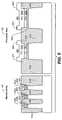
- FIG. 1shows a block diagram of a memory system 100 having a memory array 110 and peripheral area.
- FIG. 2shows a top-view of portions of a memory chip that has memory system 100 including a portion of memory array 110 and a portion of peripheral area 120 .
- FIG. 3shows the portions of the memory chip of FIG. 2 at an intermediate stage of fabrication in cross-section after formation of gate oxide layers, first polysilicon floating gate layer, SiN layer and STI structures in both memory array and peripheral area.
- FIG. 4shows the chip of FIG. 3 after removal of the SiN portions that overlie FG 1 portions.
- FIG. 5shows the chip of FIG. 4 after deposition of a second polysilicon floating gate layer and a photoresist etch mask.
- FIG. 6shows the chip of FIG. 5 after an etch to remove exposed portions of the second floating gate layer, leaving protrusions of polysilicon above the STI surface.
- FIG. 7shows the chip of FIG. 6 after deposition of a third polysilicon layer across the substrate.
- FIG. 8shows the chip of FIG. 7 after planarization of the second and third gate layers down to the level of the substantially planar upper surface of the third gate layer.
- FIG. 9shows the chip of FIG. 8 during ion implantation through the third gate layer into the upper portions of the STI structures.
- FIG. 10shows the chip of FIG. 9 after removal of the second and third gate layers down to the level of the top of the STI structures
- FIG. 11shows the chip of FIG. 10 after selective removal of implanted STI oxide.
- FIG. 12shows the chip of FIG. 11 after deposition of a dielectric layer across the substrate.
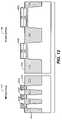
- FIG. 13shows the chip of FIG. 12 after deposition of control gate polysilicon over the dielectric layer to form a control gate layer.
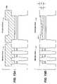
- FIG. 14shows a more detailed view of a floating gate similar to those of FIG. 13 .
- FIG. 15Ashows a cross-section of a structure like that of FIG. 5 prior to CMP.
- FIG. 15Bshows a cross-section of the structure of FIG. 15A after CMP.
- FIG. 16is a flowchart of the process described in FIGS. 3-14 .
- FIG. 1An example of a memory system 100 incorporating the various aspects of the present invention is generally illustrated in the block diagram of FIG. 1 .
- a large number of individually addressable memory cellsare arranged in a regular array 110 of rows and columns, although other physical arrangements of cells are certainly possible.
- Bit linesdesignated herein to extend along columns of the array 110 , are electrically connected with a bit line decoder and driver circuit 130 through lines 150 .
- Word lineswhich are designated in this description to extend along rows of the array 110 , are electrically connected through lines 170 to a word line decoder and driver circuit 190 .
- Each of the decoders 130 and 190receives memory cell addresses over a bus 160 from a memory controller 180 .
- the decoder and driving circuitsare also connected to the controller 180 over respective control and status signal lines 135 and 195 .
- the controller 180is connectable through lines 140 to a host device (not shown).
- the hostmay be a personal computer, notebook computer, digital camera, audio player, various other hand held electronic devices, and the like.
- the memory system 100 of FIG. 1will commonly be implemented in a card according to one of several existing physical and electrical standards, such as one from the PCMCIA, the CompactFlashTM Association, the MMCTM Association, and others.
- the lines 140terminate in a connector on the card that interfaces with a complementary connector of the host device.
- the electrical interface of many cardsfollows the ATA standard, wherein the memory system appears to the host as if it was a magnetic disk drive. Other memory card interface standards also exist.
- a memory cardmay not have a controller and the functions of the controller may be carried out by the host.
- a memory system of the type shown in FIG. 1may be permanently embedded in the host device.
- the decoder and driver circuits 130 and 190generate appropriate voltages in their respective lines of the array 110 , as addressed over the bus 160 , according to control signals in respective control and status lines 135 and 195 , to execute programming, reading and erasing functions. Any status signals, including voltage levels and other array parameters, are provided by the array 110 to the controller 180 over the same control and status lines 135 and 195 .
- a plurality of sense amplifiers within the circuit 130receive current or voltage levels that are indicative of the states of addressed memory cells within the array 110 , and provides the controller 180 with information about those states over lines 145 during a read operation.
- a large number of sense amplifiersare usually used in order to be able to read the states of a large number of memory cells in parallel.
- one row of cellsis typically addressed at a time through the circuits 190 for accessing a number of cells in the addressed row that are selected by the circuit 130 .
- all cells in each of many rowsare typically addressed together as a block for simultaneous erasure.
- Circuits such as decoder and driver circuits 130 and 190may be considered to be peripheral circuits.
- Any circuit in memory system 100 that is outside memory array 110may be considered to be a peripheral circuit and the area where such circuits are formed may be considered a peripheral area 120 .
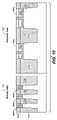
- FIG. 2A plan view of the NAND memory cell array 110 formed on a silicon substrate is shown in FIG. 2 , wherein a small part of its repetitive structure of conductive elements is illustrated with little detail of dielectric layers that exist between the elements, for clarity of explanation.
- Shallow Trench Isolation (STI) structures 210 a - 210 dare formed extending through the surface of the substrate.
- the STI regionsare shown to be spaced apart in a first x-direction, with lengths extending in a second y-direction, these first and second directions being essentially orthogonal with each other.
- each string 220 a - 220 cincludes many memory devices connected in series.
- FIG. 2shows portions of three such strings 220 a - 220 c with three memory cells shown for each string.
- strings 220 a - 220 ccontain additional cells that are not shown in FIG. 2 .
- the array 110contains additional strings that are not represented in FIG. 2 . This type of array may have thousands of strings with 16 , 32 or more cells in each string.
- a memory cellincludes a floating gate 230 and conductive source/drain regions 240 a and 240 b in the substrate adjacent to the floating gate, on either side in the y-direction. Strings are separated by STI structures 210 a - 210 d . STI structures 210 a - 210 d form isolating elements that electrically isolate source/drain regions from other source/drain regions of cells in adjacent strings. Along the y-direction source/drain regions 240 a - 240 c are shared by adjacent cells. The source/drain regions 240 a - 240 c electrically connect one cell to the next cell thus forming a string of cells. The source/drain regions 240 a - 240 c in this example are formed by implanting impurities into the substrate in the required areas.
- Word lines 250 a - 250 care shown extending across the array in the x-direction in FIG. 2 .
- the word lines 250 a - coverlie portions of the floating gates and also partially surround the floating gates. Similar arrays to the one shown are described in U.S. patent application Ser. No. 10/799,060, filed on Mar. 12, 2004, which application is hereby incorporated by reference in its entirety.
- FIG. 2also shows a portion of the peripheral area 120 .
- devicesare formed in peripheral area 120 at the same time that the memory array is formed.
- Devices in peripheral area 120may be larger than those of the memory array 110 .
- certain large high-voltage devicesmay be formed in peripheral area 120 .
- Large STI structures 210 x , 210 yare formed in peripheral area 120 . Descriptions of memory systems having memory arrays and peripheral circuits and certain processes for forming them are given in U.S. patent application Ser. Nos. 11/021,693 and 11/020,402, both filed on Dec. 22, 2004, which applications are hereby incorporated by reference in their entirety.
- metal conductor layersare metal conductor layers. Since the polysilicon elements usually have a conductivity that is significantly less than that of metal, metal conductors are included in separate layers with connections made to respective metal lines through any intermediate layers at periodical intervals along the lengths of the polysilicon elements.
- the word linemay include a metal or metal-silicide portion to increase the electrical conductivity of the word line.
- a refractory metalsuch as Cobalt or Tungsten may be used to form a silicide layer on top of the polysilicon layer.
- the silicide materialhas a higher conductivity than the polysilicon and thus improves electrical conduction along the word line.
- FIG. 3shows a cross-section of the memory array 110 and peripheral area 120 of FIG. 2 at an intermediate stage of array fabrication.
- FIG. 3shows a cross-section along the x-direction, indicated in FIG. 2 by I-I.
- gate dielectric layers, a first floating gate layer (FG 1 ) and silicon nitride layer (SiN)have been formed and divided by formation of STI structures 210 a - 210 d , 210 x - 210 z into portions of gate dielectric material 302 a - 302 c , 304 x , 304 y , portions of first floating gate material 306 a - 306 c , 306 x , 306 y and portions of silicon nitride 308 a - 308 c , 308 x , 308 y .
- a thin gate dielectric layermay be used in the memory array while a same or different gate dielectric layer thickness is used for peripheral circuits.
- approximately 70-90 Angstroms of gate dielectricis used in the memory array to form portions of gate dielectric 302 a - 302 c
- 300-400 Angstroms of gate dielectricis used to form dielectric portions 304 x , 304 y for high voltage peripheral circuits in peripheral area 120 .
- FG 1 and SiN layersare formed over the gate dielectric layers.
- STI structures 210 a - 210 d , 210 x - 210 yare formed.
- a photoresist mask layermay be used to define the locations of the STI structures 210 a - 210 d , 210 x - 210 y .
- the SiNis then etched according to the photoresist mask layer into portions 308 a - 308 c , 308 x , 308 y .
- SiN portions 308 a - 308 c , 308 x , 308 yform a hard-mask for subsequent trench etching.
- the trencheshave a width that is equal to the minimum feature size of the process used and are separated by a distance that is also equal to the minimum feature size.
- the minimum feature sizeis 55 nanometers in the present example, but aspects of the present invention may be applied to circuits of any size.
- a high-density memory arraymay be formed. Larger trenches may be formed in the peripheral area.
- the trenchesare then filled with a suitable dielectric.
- a High Density Plasma (HDP) oxide processis used for filling the STI trenches.
- Silicon dioxide (oxide)is used for trench fill.
- filling STI trenches with dielectricis done by overfilling with dielectric material and subsequently removing excess dielectric material using a HDP etch-back process.
- HDPHigh Density Plasma
- oxideis deposited to a thickness that fills STI trenches and covers the SiN portions 308 a - 308 c , 308 x , 308 y .
- the oxidemay then be planarized by CMP, leaving some oxide over SiN portions 308 a - 308 c , 308 x , 308 y so that SiN portions 308 a - 308 c , 308 x , 308 y are not damaged by CMP.
- the thickness of the oxide layer over SiN portions 308 a - 308 c , 308 x , 308 ymay be measured and an etch-back process may be performed to remove this layer.
- this etch-backis done with an over-etch of about 50 Angstroms so that SiN portions 308 a - 308 c , 308 x , 308 y extend above the level of the STI structures 210 a - 210 d , 210 x - 210 z and no oxide remains over SiN portions 308 a - 308 c , 308 x , 308 y.
- FIG. 3shows three portions 306 a - 306 c of FG 1 and three portions 308 a - 308 c of SiN in memory array 110 that are separated by STI structures 210 a - 210 d .
- Two additional portions 306 x , 306 y of FG 1 and two additional portions 308 x , 308 y of SiNare shown in peripheral area 120 .
- the FG 1 portions 306 a - 306 c , 306 x , 306 y and SiN portions 308 a - 308 c , 308 x , 308 yare strips at this stage and are later formed into individual units.
- the structuresare closely packed in the memory array but are more widely spaced in the peripheral area.
- the aspect ratiois of particular concern.
- the SiN, gate oxide and the FG 1 layer thicknesses, together with the STI depth divided by the width of the STI structurecan give an aspect ratio of between 4 and 5.8.
- An aspect ratio of less than 6.0has been found to provide acceptable results with the HDP oxide deposition process used in this example.
- Other processesmay have other ranges of acceptable aspect ratio and the current invention is not limited to any particular deposition scheme or aspect ratio.
- SiN portions 308 a - 308 c , 308 x , 308 yare removed. These portions may be removed using a hot Phosphoric Acid (H3PO4) etch to leave cavities 420 a - 420 c , 420 x , 420 y over FG 1 portions 306 a - 306 c , 306 x , 306 y as shown in FIG. 4 . Subsequent to removal of the SiN portions 308 a - 308 c , 308 x , 308 y a cleaning process may be performed.
- H3PO4hot Phosphoric Acid
- a clean with dilute Hydrofluoric Acidremoves a small amount of oxide (approximately 50 Angstroms) of STI portions 210 a - 210 c , 210 x - 210 z and thus widens the cavities 420 a - 420 c , 420 x , 420 y .
- FIG. 4shows the same view as in FIG. 3 after removal of SiN portions 308 a - 308 c , 308 x , 308 y and cleaning.
- Cavities 420 a - 420 cfor example, can have a depth of 500-600 Angstroms and a width of approximately 650 Angstroms in memory array 110 .
- SiN portions 308 a - 308 c , 308 x , 308 yact as placeholders that establish locations but are later removed. Because the SiN itself is removed, its properties are not critical and other materials could also be used for this purpose. SiN portions 308 a - 308 c , 308 x , 308 y may be considered as dummy portions because they are later replaced. SiN portions 308 a - 308 c , 308 x , 308 y also act as a hard-mask for trench etching so that they serve a dual purpose.
- FIG. 5shows the same view as FIG. 4 with an additional polysilicon layer FG 2 overlying FG 1 portions 306 a - 306 c , 306 x , 306 y and overlying STI structures 210 a - 210 d , 210 x - 210 z .
- FG 2is approximately 800-900 Angstroms thick.
- FG 2is in direct contact with FG 1 portions 306 a - 306 c , 306 x , 306 y so that they are electrically connected.
- portions of FG 2are covered with photoresist masking layer portions 530 , 531 .
- photoresist masking layer portions 530 , 531Such layers are well known and may be formed by spinning on photoresist, then exposing the photoresist to UV light according to a predetermined pattern and removing portions of the photoresist according to whether they were exposed.
- the photoresist portions 530 , 531are shown extending over the parts of the FG 2 layer that overlie FG 1 portions 306 x , 306 y and also extending beyond these parts to overlie parts of the FG 2 layer that overlie edges of STI structures 210 x - 210 z .
- the memory array 110is uncovered, as are central portions of the wide STI structures 210 x - 210 z in peripheral area 120 .
- An etchis then performed to remove exposed parts of the FG 2 layer (parts not covered by the photoresist portions 530 , 531 ).
- FIG. 6shows the result of removal of the exposed parts of the FG 2 layer.
- the removal of these parts of FG 2(FG 2 etch-back) is stopped when the etch reaches STI structures 210 a - 210 d , 210 x - 210 z so that FG 2 portions in cavities 420 a - 420 c , 420 x , 420 y remain.
- the tops of the remaining FG 2 portions 640 a - 640 care at approximately the same level as the tops of STI structures 210 a - 210 d that separate them at this point providing a substantially planar surface in the memory array 110 .
- FG 2 portions 640 a - 640 chave replaced SiN portions 308 a - 308 c at this point.
- Thisprovides a floating gate structure consisting of FG 1 portions 306 a - 306 c and FG 2 portions 640 a - 640 c that are self-aligned to the STI structures 210 a - 210 d and are equal in height to the STI structures 210 a - 210 d .
- this processreplaces SiN portions 308 a - 308 c with FG 2 portions 640 a - 640 c and thereby makes a floating gate that is as high as the upper surface of the hard-mask used to form the STI trenches.
- Many prior systemshave a hard-mask SiN layer that overlies both FG 1 and FG 2 layers but is not replaced. Thus, for a given thickness of FG 1 and FG 2 this requires a higher aspect ratio STI structure.
- the present processprovides a higher floating gate by reusing the space that was occupied by the SiN hard-mask portions for additional floating gate height.
- photoresist portions 530 , 531are removed after FG 2 etch-back, leaving FG 2 portions 640 x , 640 y that protrude above the level of the STI structures 210 x - 210 z . Because raised portions 651 - 654 of the FG 2 layer that extend over STI structures 210 x - 210 z were masked, these portions remain and extend approximately 800-900 Angstroms above the level of STI structures 210 x - 210 z .
- FG 2 layer 640 a - 640 cextend slightly above the STI structures 210 c - 210 d in the memory array region after the clean.
- another conductive layeris deposited.
- FG 3is deposited across the substrate.
- FIG. 7shows the same view as FIG. 6 after deposition of the FG 3 layer.
- This layerextends over both memory array 110 and peripheral area 120 .
- the FG 3 layer shownconsists of approximately 400-600 Angstroms of doped polysilicon.
- the FG 3 layeris substantially planar because the underlying FG 2 portions 640 a - 640 c and STI structures 210 a - 210 d are approximately the same height (a difference of approximately 50 Angstroms).
- FG 3has a substantially planar upper surface in memory array 110 and over central portions of the wide STI structures 210 x - 210 z of peripheral area 120 .
- peripheral area 120there is a hill and valley profile with protrusions 651 - 654 extending upwards where the FG 2 portions 640 x , 640 y overlie STI structures 210 x - 210 z .
- Protrusions 651 - 654may extend 1200-1300 Angstroms above the upper surface of the STI structures 210 x - 210 z at this point.
- Protrusions 651 - 654may be removed by performing a soft Chemical Mechanical Polishing (CMP) to remove only protrusions 651 - 654 without significantly affecting the flat upper surface of the FG 3 layer.
- CMPChemical Mechanical Polishing
- a soft CMP processinvolves using standard CMP apparatus and slurry but with very little pressure applied between the substrate and the pad. This provides enough pressure to ensure that protrusions are eroded, while not eroding the flat portions of the substrate.
- FIG. 8shows the result of a soft CMP process applied to the structures shown in FIG. 7 .
- the CMP processremoves protrusions 651 - 654 but stops when the flat portions of the FG 3 layer (those portions in memory array 110 and over central parts of wide STI structures 210 x - 210 z in peripheral area 120 ) begin to be eroded. In some cases, a limited amount of erosion of these areas may be desirable to fully planarize the FG 3 layer.
- the CMP processmay be stopped by endpoint detection or by timing.
- the resultis a highly planarized polysilicon surface extending across the substrate overlying FG 2 portions 640 a - 640 c , 640 x , 640 y and STI structures 210 a - 210 d , 210 x - 210 z.
- Ionsare implanted through the FG 3 layer into the underlying STI structures 210 a - 210 d , 210 x - 210 z in FIG. 9 .
- This implantation processmay be done so that the ions are implanted to a predetermined depth.
- An implant energymay be selected so that the implanted ions do not penetrate below a certain level to a significant extent.
- the implant damage and concentration of implanted ionscan be largely confined to a top implanted layer 970 of STI structures 210 a - 210 d , 210 x - 210 z and little implant damage or implanted ion concentration may exist below implanted top layer 970 .
- implanted layer 970may extend to a depth of approximately 700 Angstroms into the STI structures 210 a - 210 d , 210 x - 210 z .
- the implanted layer 970may extend to a depth of 500 Angstroms in other examples.
- the oxide of implanted layer 970has a high concentration of implanted species and a significant amount of implant damage while the oxide below this level has a low concentration of implanted species and little or no implant damage.
- Phosphorus ions (Ph+) and Silicon ions (Si+)are suitable for implantation in this step.
- the conductive FG 3 layerprovides protection against charging of the FG 1 and FG 2 portions.
- the FG 3 layerconnects all FG 2 portions 640 a - 640 c , 640 x , 640 y and FG 1 portions 306 a - 306 c , 306 x , 306 y together. Also, the FG 3 layer is generally formed in a furnace process so that FG 3 extends around the substrate to form an electrically continuous layer that may be in contact with a chuck or support.
- the FG 3 layerallows any electrical charge that could build up in implanted layer 970 to discharge by flowing through the FG 3 layer and then away from the substrate.
- the FG 3 layermay be removed. This is done by CMP or etch of the polysilicon layers down to the level of the top of the STI structures 210 a - 210 d , 210 x - 210 z as shown in FIG. 10 . Both the FG 3 layer and portions of FG 2 are removed in this step. At this point, the upper surface of the substrate is flat because the FG 2 portions 640 a - 640 c , 640 x , 640 y are leveled with STI structures 210 a - 210 d , 210 x - 210 z .
- the wide FG 2 portions 640 x , 640 y of peripheral area 120may be planarized without dishing by this step because at the start of this step the upper surface of the polysilicon layer was substantially planar.
- FIG. 11shows the result of the removal of implanted layer 970 of the STI structures 210 a - 210 c , 210 x - 210 z .
- the oxide that is removed from the STI structuresis the oxide that is implanted.
- Implanted oxidehas a higher etch rate than unimplanted oxide. Thus, ion implantation is used to increase the etch rate of the upper layer of oxide while leaving the rest of the oxide largely unchanged.
- Thisprovides a way to selectively etch only the implanted layer of oxide 970 and to stop at a predetermined depth that is established by ion implantation.
- the etch ratemay be higher for implanted oxide because of damage caused by ions and also because of the chemical effects of the presence of ions.
- An etch chemistrymay be chosen to be compatible with the particular ion implantation scheme used. For example, depending on the implanted species (p-type or n-type) a suitable etch may be chosen that will preferentially etch oxide with that species.
- the etch rate for implanted oxidemay be more than double that of unimplanted oxide. Where implantation is not used to control etch depth, underetching and overetching may occur leading to poor device performance or device failure. In the present example, oxide etch-back is achieved with a wet-etch using a dilute Hydrofluoric acid (HF) followed by an additional Reactive Ion Etch (RIE).
- HFdilute Hydrofluoric acid
- RIEReactive
- a dielectric layer 1274is deposited over the surface of the substrate including FG 2 portions 640 a - 640 c , 640 x , 640 y and STI structures 210 a - 210 d , 210 x - 210 z as shown in FIG. 12 .
- Dielectric layer 1274may be an oxide or nitride layer or may be a compound layer made up of sublayers such as oxide-nitride-oxide (ONO).
- ONOoxide-nitride-oxide
- FIG. 13shows the substrate with a conductive layer 1380 overlying dielectric layer 1274 .
- Conductive layer 1380is used to form control gates.
- Control gatesare generally formed by patterning conductive layer 1380 into strips (wordlines) that extend across the substrate surface in a direction perpendicular to STI structures 210 a - 210 d in memory array 110 .
- Floating gatesmay be formed by the same step by etching exposed parts of the floating gate portions (FG 1 portions 306 a - 306 c and FG 2 portions 640 a - 640 c ) that are between wordlines.
- the structure shownprovides a large coupling area between the floating gates and control gates as shown in more detail in FIG. 14 .
- the floating gate 1482is a typical floating gate of memory array 110 and is made up of an FG 1 portion 1482 a and an FG 2 portion 1482 b .
- the control gate 1480extends vertically between floating gates to a depth D 1 , so that extensions 1480 a , 1480 b of the control gate 1480 extend into the gaps where implanted layer 970 of STI structures 210 a - 210 d was removed.
- Control gate extensions 1480 a , 1480 bprovide two benefits. Firstly, they increase the coupling area between floating gate 1482 and control gate 1480 . Secondly, they reduce coupling between adjacent floating gates by providing a conductive barrier between them.
- control gate extensions 1480 a , 1480 b and gate dielectric 1486should be at least as great as the thickness of the gate dielectric 1486 .
- variation in the etched depthmay occur.
- the depth of the etchmay be controlled to a higher precision and device uniformity may be improved.
- Table 2shows some simulation results for memory cells having two different oxide etch-back depths (and thus, two different control gate extension lengths).
- Total Yuprefers to the Yupin effect between neighboring cells.
- Yupin effectis a term used to describe the undesirable coupling between neighboring cells whereby the charge level of one floating gate affects the threshold voltage of a neighboring cell. This effect is described in detail in U.S. Pat. No. 5,867,429, which patent is incorporated by reference in its entirety. Thus, it can be seen that Yupin effect increases when D 1 is reduced from 60 nm to 50 nm, eventually affecting device performances.
- FIG. 15Ashows a cross-section of a structure like that of FIG. 5 prior to planarization.
- FIG. 15Bshows the results of planarizing the structure of 15 A.
- a substantially planar surfaceis produced in memory array 110 .
- the polysilicon of FG 1 layer 1580suffers dishing during CMP.
- the resulting FG 2 portion 1581has a thickness of T 2 at the edges of a large FG 2 structure but has a thickness of T 1 in the middle.
- T 1is less than T 2 so that the cross-sectional area is reduced and the resistance of such a structure is increased.
- Dishingis the result of CMP erosion at the bottom of a wide depression while planarizing the surface.
- a soft etchmay selectively remove the protrusions down to the level of the upper surface over the rest of the substrate and thus form a highly planarized surface.
- FIG. 8shows a substantially planar upper polysilicon surface of FG 2 and FG 3 portions. Later applying CMP to this surface provides FG 2 portions (in FIG. 10 ) that do not significantly suffer from dishing. Control of the thickness of FG 2 portions in the peripheral area is particularly important because these portions may be used as resistors. By providing protrusions and adding an additional polysilicon layer, better control of FG 2 thickness in the peripheral area and avoidance of dishing may be achieved. In some embodiments, such control of FG 2 thickness may not be so critical. In these cases, the FG 2 layer shown in FIG. 5 may be planarized by CMP to provide a similar result to that shown in FIG. 15B .
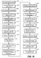
- FIG. 16is a flowchart of the process steps described above.
- gate dielectric layersare formed over different areas of the substrate 1601 .
- a first floating gate (FG 1 ) layeris formed 1603 over the gate dielectric layers and a Silicon Nitride (SiN) layer is formed 1605 over the FG 1 layer.
- a patterned photoresist layeris formed 1607 over the SiN layer and the SiN layer is etched 1609 into separate portions according to the pattern.
- the photoresistis then removed 1611 .
- the remaining SiN portionsare then used as a hard-mask to etch STI trenches 1613 .
- the trenchesare filled with HDP oxide and etched-back 1615 .
- SiN portionsare removed 1617 and a cleaning step is (optionally) performed to open the cavities left after SiN removal 1619 .
- a second floating gate layer (FG 2 )is then deposited 1621 . Portions of FG 2 in the peripheral area are covered 1623 . The covered portions extend over FG 1 portions and extend out over the edges of the adjacent STI structures. Uncovered portions of FG 2 are then removed 1625 . Then, the photoresist is removed 1627 leaving protrusions of FG 2 over the STI structures.
- a third floating gate (FG 3 ) layeris formed 1629 and includes protrusions where FG 3 overlies FG 2 protrusions.
- a soft CMP stepis performed 1631 to remove protrusions and planarize the substrate to the level of the top surface of the FG 3 layer over the STI structures.
- ionsare implanted 1633 through the conductive polysilicon into the STI oxide to a predetermined depth.
- the polysiliconis then removed 1635 down to the level of the top surface of the STI structures.
- Implanted STIis then selectively etched away 1637 .
- a dielectric layeris formed 1639 over the floating gate portions and a conductive control gate layer is formed 1641 over the dielectric layer.
- Wordlinesare formed 1643 by etching the control gate layer into separate strips.
Landscapes
- Engineering & Computer Science (AREA)
- Manufacturing & Machinery (AREA)
- Microelectronics & Electronic Packaging (AREA)
- General Physics & Mathematics (AREA)
- Condensed Matter Physics & Semiconductors (AREA)
- Computer Hardware Design (AREA)
- Physics & Mathematics (AREA)
- Power Engineering (AREA)
- Chemical & Material Sciences (AREA)
- Chemical Kinetics & Catalysis (AREA)
- General Chemical & Material Sciences (AREA)
- Inorganic Chemistry (AREA)
- Semiconductor Memories (AREA)
- Non-Volatile Memory (AREA)
- Element Separation (AREA)
Abstract
Description
| TABLE 1 |
| Implant simulation results: |
| With Ph+ implant dose: 1.0E15 atm/cm2. |
| FG3 Thickness = 500 A. |
| Energy | Concentration | Oxide Depth |
| 20 KeV | 8.3E17 atm/cm3 | 280 A |
| 8.3E14 atm/cm3 | 560 A | |
| TABLE 2 |
| Cell Simulation Results: |
| FG1 Width: | 50 | nm | 50 | nm | |
| FG2 Width: | 60 | nm | 60 | nm | |
| EB Amount, D1: | 60 | nm | 50 | nm | |
| Channel L: | 51 | nm | 51 | nm |
| →Coupling Ratio | 49.8% | 46.7% |
| →Total Yup | 446 | mV | 534 | mV | ||
The results are for two cells having identical FG1 and FG2 dimensions and channel lengths. The results show that if the etch-back amount (D1) is decreased from 60 nm to 50 nm (600 Angstroms to 500 Angstroms), the coupling ratio drops from 49.8% to 46.7% and coupling between neighboring cells increases. “Total Yup” refers to the Yupin effect between neighboring cells. “Yupin effect” is a term used to describe the undesirable coupling between neighboring cells whereby the charge level of one floating gate affects the threshold voltage of a neighboring cell. This effect is described in detail in U.S. Pat. No. 5,867,429, which patent is incorporated by reference in its entirety. Thus, it can be seen that Yupin effect increases when D1 is reduced from 60 nm to 50 nm, eventually affecting device performances.
Claims (12)
Priority Applications (9)
| Application Number | Priority Date | Filing Date | Title |
|---|---|---|---|
| US11/254,142US7541240B2 (en) | 2005-10-18 | 2005-10-18 | Integration process flow for flash devices with low gap fill aspect ratio |
| JP2008536692AJP4950207B2 (en) | 2005-10-18 | 2006-10-10 | Integrated flow for low gap fill aspect ratio flash devices |
| PCT/US2006/039931WO2007047390A2 (en) | 2005-10-18 | 2006-10-10 | Integration process flow for flash devices |
| CN200680036254.2ACN101288164B (en) | 2005-10-18 | 2006-10-10 | Integrated Process Flow for Flash Devices |
| EP11001492AEP2320455B1 (en) | 2005-10-18 | 2006-10-10 | Method of planarizing for flash memory device fabrication |
| AT06825851TATE526682T1 (en) | 2005-10-18 | 2006-10-10 | INTEGRATION PROCESS FLOW FOR FLASH DEVICES WITH LOW GAP FILL ASPECT RATIO |
| KR1020087007369AKR101029696B1 (en) | 2005-10-18 | 2006-10-10 | Integration process flow for flash devices with low gap fill aspect ratio |
| EP06825851AEP1938371B1 (en) | 2005-10-18 | 2006-10-10 | Integration process flow for flash devices with low gap fill aspect ratio |
| TW095138445ATWI384588B (en) | 2005-10-18 | 2006-10-18 | Integration process flow for flash devices with low gap fill aspect ratio |
Applications Claiming Priority (1)
| Application Number | Priority Date | Filing Date | Title |
|---|---|---|---|
| US11/254,142US7541240B2 (en) | 2005-10-18 | 2005-10-18 | Integration process flow for flash devices with low gap fill aspect ratio |
Publications (2)
| Publication Number | Publication Date |
|---|---|
| US20070087504A1 US20070087504A1 (en) | 2007-04-19 |
| US7541240B2true US7541240B2 (en) | 2009-06-02 |
Family
ID=37635752
Family Applications (1)
| Application Number | Title | Priority Date | Filing Date |
|---|---|---|---|
| US11/254,142Active2026-04-09US7541240B2 (en) | 2005-10-18 | 2005-10-18 | Integration process flow for flash devices with low gap fill aspect ratio |
Country Status (8)
| Country | Link |
|---|---|
| US (1) | US7541240B2 (en) |
| EP (2) | EP1938371B1 (en) |
| JP (1) | JP4950207B2 (en) |
| KR (1) | KR101029696B1 (en) |
| CN (1) | CN101288164B (en) |
| AT (1) | ATE526682T1 (en) |
| TW (1) | TWI384588B (en) |
| WO (1) | WO2007047390A2 (en) |
Cited By (12)
| Publication number | Priority date | Publication date | Assignee | Title |
|---|---|---|---|---|
| US20070235794A1 (en)* | 2006-03-21 | 2007-10-11 | Semiconductor Energy Laboratory Co., Ltd. | Nonvolatile semiconductor memory device |
| US20080002470A1 (en)* | 2006-06-28 | 2008-01-03 | Hideyuki Kinoshita | NAND nonvolatile semiconductor memory device and method of manufacturing NAND nonvolatile semiconductor memory device |
| US20080237685A1 (en)* | 2007-03-26 | 2008-10-02 | Samsung Electronics Co., Ltd. | Semiconductor memory device, method of fabricating the same, and devices employing the semiconductor memory device |
| US20100190329A1 (en)* | 2008-12-29 | 2010-07-29 | Semiconductor Manufacturing International (Shanghai) Corporation | Method and structure for performing a chemical mechanical polishing process |
| US8603891B2 (en) | 2012-01-20 | 2013-12-10 | Micron Technology, Inc. | Methods for forming vertical memory devices and apparatuses |
| US9406784B1 (en) | 2015-02-02 | 2016-08-02 | Powerchip Technology Corporation | Method of manufacturing isolation structure and non-volatile memory with the isolation structure |
| US20170194189A1 (en)* | 2016-01-06 | 2017-07-06 | Semiconductor Manufacturing International (Shanghai) Corporation | Method for manufacturing memory device |
| US9754788B2 (en)* | 2015-07-13 | 2017-09-05 | United Microelectronics Corp. | Manufacturing method of semiconductor structure including planarizing a polysilicon layer over an array area and a periphery area |
| US10566337B2 (en)* | 2018-04-16 | 2020-02-18 | Winbond Electronics Corp. | Method of manufacturing memory device |
| TWI733013B (en)* | 2018-03-29 | 2021-07-11 | 聯華電子股份有限公司 | Semiconductor fabrication method |
| US11251273B2 (en)* | 2018-07-24 | 2022-02-15 | Winbond Electronics Corp. | Non-volatile memory device and method for manufacturing the same |
| US11257836B2 (en) | 2020-02-05 | 2022-02-22 | Macronix International Co., Ltd. | Dummy vertical structures for etching in 3D NAND memory and other circuits |
Families Citing this family (25)
| Publication number | Priority date | Publication date | Assignee | Title |
|---|---|---|---|---|
| US7541240B2 (en) | 2005-10-18 | 2009-06-02 | Sandisk Corporation | Integration process flow for flash devices with low gap fill aspect ratio |
| US7737483B2 (en)* | 2005-12-06 | 2010-06-15 | Sandisk Corporation | Low resistance void-free contacts |
| US7615448B2 (en)* | 2005-12-06 | 2009-11-10 | Sandisk Corporation | Method of forming low resistance void-free contacts |
| US20090321806A1 (en)* | 2008-06-26 | 2009-12-31 | Len Mei | Nonvolatile memory with floating gates with upward protrusions |
| US8026544B2 (en) | 2009-03-30 | 2011-09-27 | Sandisk Technologies Inc. | Fabricating and operating a memory array having a multi-level cell region and a single-level cell region |
| US8415238B2 (en) | 2010-01-14 | 2013-04-09 | International Business Machines Corporation | Three dimensional integration and methods of through silicon via creation |
| CN102412182B (en)* | 2010-09-19 | 2015-09-02 | 中芯国际集成电路制造(上海)有限公司 | Formation method of shallow trench isolation structure |
| US8383515B2 (en)* | 2010-11-16 | 2013-02-26 | Macronix International Co., Ltd. | Methodology for wordline short reduction |
| US20130020640A1 (en)* | 2011-07-18 | 2013-01-24 | Chen John Y | Semiconductor device structure insulated from a bulk silicon substrate and method of forming the same |
| US8946792B2 (en)* | 2012-11-26 | 2015-02-03 | International Business Machines Corporation | Dummy fin formation by gas cluster ion beam |
| JP6255692B2 (en)* | 2013-03-29 | 2018-01-10 | 富士通セミコンダクター株式会社 | Manufacturing method of semiconductor device |
| US9673207B2 (en)* | 2015-08-20 | 2017-06-06 | Sandisk Technologies Llc | Shallow trench isolation trenches and methods for NAND memory |
| CN106486377B (en)* | 2015-09-01 | 2019-11-29 | 中芯国际集成电路制造(上海)有限公司 | Fin type semiconductor devices and its manufacturing method |
| CN106409836A (en)* | 2016-11-21 | 2017-02-15 | 武汉新芯集成电路制造有限公司 | Manufacturing method of flash memory unit |
| US20180269226A1 (en)* | 2017-03-16 | 2018-09-20 | Toshiba Memory Corporation | Semiconductor memory device and method for manufacturing same |
| TWI720241B (en)* | 2017-08-17 | 2021-03-01 | 聯華電子股份有限公司 | Method for manufacturing semiconductor structure |
| CN108109656B (en)* | 2017-12-28 | 2020-10-27 | 上海华力微电子有限公司 | Flash memory array and manufacturing method thereof |
| CN108321087B (en)* | 2018-01-31 | 2019-03-26 | 武汉新芯集成电路制造有限公司 | A kind of forming method of floating gate |
| US10804281B2 (en) | 2018-09-28 | 2020-10-13 | Taiwan Semiconductor Manufacturing Co., Ltd. | Anti-dishing structure for embedded memory |
| KR102613856B1 (en)* | 2019-06-21 | 2023-12-14 | 에프이아이 컴파니 | Perimeter trench formation and delineation etch delayering |
| US11329128B2 (en) | 2019-08-29 | 2022-05-10 | Taiwan Semiconductor Manufacturing Company, Ltd. | High voltage device with gate extensions |
| TWI777225B (en)* | 2019-08-29 | 2022-09-11 | 台灣積體電路製造股份有限公司 | Integrated chip and method of forming the same |
| CN111162077B (en)* | 2020-01-02 | 2022-07-22 | 长江存储科技有限责任公司 | Semiconductor structure and forming method thereof |
| US11329064B2 (en)* | 2020-06-16 | 2022-05-10 | Micron Technology, Inc. | Integrated assemblies and methods of forming integrated assemblies |
| TWI825868B (en)* | 2022-05-26 | 2023-12-11 | 南亞科技股份有限公司 | Semiconductor device with programmable feature |
Citations (101)
| Publication number | Priority date | Publication date | Assignee | Title |
|---|---|---|---|---|
| US5043940A (en) | 1988-06-08 | 1991-08-27 | Eliyahou Harari | Flash EEPROM memory systems having multistate storage cells |
| US5070032A (en) | 1989-03-15 | 1991-12-03 | Sundisk Corporation | Method of making dense flash eeprom semiconductor memory structures |
| US5095344A (en) | 1988-06-08 | 1992-03-10 | Eliyahou Harari | Highly compact eprom and flash eeprom devices |
| US5168465A (en) | 1988-06-08 | 1992-12-01 | Eliyahou Harari | Highly compact EPROM and flash EEPROM devices |
| US5172338A (en) | 1989-04-13 | 1992-12-15 | Sundisk Corporation | Multi-state EEprom read and write circuits and techniques |
| US5198380A (en) | 1988-06-08 | 1993-03-30 | Sundisk Corporation | Method of highly compact EPROM and flash EEPROM devices |
| JPH05190809A (en) | 1992-01-14 | 1993-07-30 | Kawasaki Steel Corp | Method for manufacturing semiconductor device |
| US5268319A (en) | 1988-06-08 | 1993-12-07 | Eliyahou Harari | Highly compact EPROM and flash EEPROM devices |
| US5268318A (en) | 1988-06-08 | 1993-12-07 | Eliyahou Harari | Highly compact EPROM and flash EEPROM devices |
| US5297148A (en) | 1989-04-13 | 1994-03-22 | Sundisk Corporation | Flash eeprom system |
| US5313421A (en) | 1992-01-14 | 1994-05-17 | Sundisk Corporation | EEPROM with split gate source side injection |
| US5315541A (en) | 1992-07-24 | 1994-05-24 | Sundisk Corporation | Segmented column memory array |
| US5343063A (en) | 1990-12-18 | 1994-08-30 | Sundisk Corporation | Dense vertical programmable read only memory cell structure and processes for making them |
| US5385630A (en)* | 1993-06-29 | 1995-01-31 | Digital Equipment Corporation | Process for increasing sacrificial oxide etch rate to reduce field oxide loss |
| US5389808A (en) | 1993-02-25 | 1995-02-14 | Kabushiki Kaisha Toshiba | Non-volatile semiconductor memory with increased capacitance between floating and control gates |
| US5459091A (en) | 1993-10-12 | 1995-10-17 | Goldstar Electron Co., Ltd. | Method for fabricating a non-volatile memory device |
| US5512505A (en) | 1990-12-18 | 1996-04-30 | Sandisk Corporation | Method of making dense vertical programmable read only memory cell structure |
| US5534456A (en) | 1994-05-25 | 1996-07-09 | Sandisk Corporation | Method of making dense flash EEPROM cell array and peripheral supporting circuits formed in deposited field oxide with sidewall spacers |
| US5579259A (en) | 1995-05-31 | 1996-11-26 | Sandisk Corporation | Low voltage erase of a flash EEPROM system having a common erase electrode for two individually erasable sectors |
| US5640032A (en) | 1994-09-09 | 1997-06-17 | Nippon Steel Corporation | Non-volatile semiconductor memory device with improved rewrite speed |
| US5712179A (en) | 1995-10-31 | 1998-01-27 | Sandisk Corporation | Method of making triple polysilicon flash EEPROM arrays having a separate erase gate for each row of floating gates |
| US5712180A (en) | 1992-01-14 | 1998-01-27 | Sundisk Corporation | EEPROM with split gate source side injection |
| US5716863A (en) | 1995-06-01 | 1998-02-10 | Kabushiki Kaisha Toshiba | Method of manufacturing semiconductor device having elements different in gate oxide thickness and resistive elements |
| US5756385A (en) | 1994-03-30 | 1998-05-26 | Sandisk Corporation | Dense flash EEPROM cell array and peripheral supporting circuits formed in deposited field oxide with the use of spacers |
| US5786988A (en) | 1996-07-02 | 1998-07-28 | Sandisk Corporation | Integrated circuit chips made bendable by forming indentations in their back surfaces flexible packages thereof and methods of manufacture |
| US5817580A (en) | 1996-02-08 | 1998-10-06 | Micron Technology, Inc. | Method of etching silicon dioxide |
| US5867429A (en) | 1997-11-19 | 1999-02-02 | Sandisk Corporation | High density non-volatile flash memory without adverse effects of electric field coupling between adjacent floating gates |
| US5891752A (en) | 1997-04-24 | 1999-04-06 | Eastman Kodak Company | Method for making charge coupled device with all electrodes of transparent conductor |
| US5899736A (en)* | 1997-09-19 | 1999-05-04 | Siemens Aktiengesellschaft | Techniques for forming electrically blowable fuses on an integrated circuit |
| US5923976A (en) | 1995-12-26 | 1999-07-13 | Lg Semicon Co., Ltd. | Nonvolatile memory cell and method of fabricating the same |
| US5950096A (en)* | 1997-09-22 | 1999-09-07 | Lucent Technologies Inc. | Process for improving device yield in integrated circuit fabrication |
| US5966618A (en) | 1998-03-06 | 1999-10-12 | Advanced Micro Devices, Inc. | Method of forming dual field isolation structures |
| US5981335A (en) | 1997-11-20 | 1999-11-09 | Vanguard International Semiconductor Corporation | Method of making stacked gate memory cell structure |
| US5999448A (en) | 1998-03-17 | 1999-12-07 | Fujitsu Limited | Nonvolatile semiconductor memory device and method of reproducing data of nonvolatile semiconductor memory device |
| US6046935A (en) | 1996-03-18 | 2000-04-04 | Kabushiki Kaisha Toshiba | Semiconductor device and memory system |
| US6060360A (en) | 1997-04-14 | 2000-05-09 | Taiwan Semiconductor Manufacturing Company | Method of manufacture of P-channel EEprom and flash EEprom devices |
| US6103573A (en) | 1999-06-30 | 2000-08-15 | Sandisk Corporation | Processing techniques for making a dual floating gate EEPROM cell array |
| US6151248A (en) | 1999-06-30 | 2000-11-21 | Sandisk Corporation | Dual floating gate EEPROM cell array with steering gates shared by adjacent cells |
| US6172395B1 (en) | 1997-09-26 | 2001-01-09 | Taiwan Semiconductor Manufacturing Company | Method of manufacture of self-aligned floating gate, flash memory cell and device manufactured thereby |
| US6184093B1 (en) | 1997-12-19 | 2001-02-06 | Mosel Vitelic, Inc. | Method of implementing differential gate oxide thickness for flash EEPROM |
| US6208545B1 (en) | 1997-04-04 | 2001-03-27 | Glenn J. Leedy | Three dimensional structure memory |
| WO2001024268A1 (en) | 1999-09-24 | 2001-04-05 | Intel Corporation | A nonvolatile memory device with a high work function floating-gate and method of fabrication |
| US6222762B1 (en) | 1992-01-14 | 2001-04-24 | Sandisk Corporation | Multi-state memory |
| JP2001135736A (en) | 1999-11-08 | 2001-05-18 | Nec Corp | Nonvolatile semiconductor memory and its manufacturing method |
| US6235586B1 (en) | 1999-07-13 | 2001-05-22 | Advanced Micro Devices, Inc. | Thin floating gate and conductive select gate in situ doped amorphous silicon material for NAND type flash memory device applications |
| US6258665B1 (en) | 1997-03-21 | 2001-07-10 | Kabushiki Kaisha Toshiba | Non-volatile semiconductor memory device and method for manufacturing the same |
| US6281077B1 (en) | 1998-09-11 | 2001-08-28 | Stmicroelectronics S.R. L. | Method for manufacturing electronic devices comprising non-volatile memory cells and LV transistors with salicided junctions |
| US6281075B1 (en) | 1999-01-27 | 2001-08-28 | Sandisk Corporation | Method of controlling of floating gate oxide growth by use of an oxygen barrier |
| US6295227B1 (en) | 1998-11-26 | 2001-09-25 | Kabushiki Kaisha Toshiba | Non-volatile semiconductor memory device |
| US6297097B1 (en) | 1996-05-16 | 2001-10-02 | Hyundai Electronics Industries Co., Ltd. | Method for forming a semiconductor memory device with increased coupling ratio |
| US6326263B1 (en) | 2000-08-11 | 2001-12-04 | United Microelectronics Corp. | Method of fabricating a flash memory cell |
| US6365525B2 (en) | 1998-08-18 | 2002-04-02 | Siemens Aktiengesellschaft | Method of fabricating a semiconductor insulation layer |
| US20020048897A1 (en) | 2000-05-26 | 2002-04-25 | Samsung Electronics Co., Ltd. | Method of forming a self-aligned shallow trench isolation |
| US6391722B1 (en) | 2001-07-13 | 2002-05-21 | Vanguard International Semiconductor Corporation | Method of making nonvolatile memory having high capacitive coupling ratio |
| US20020072197A1 (en) | 2000-07-25 | 2002-06-13 | Samsung Electronics Co., Ltd. | Method for self-aligned shallow trench isolation and method of manufacturing non-volatile memory device using the same |
| US6417051B1 (en) | 1999-03-12 | 2002-07-09 | Kabushiki Kaisha Toshiba | Method of manufacturing memory device including insulated gate field effect transistors |
| US6417538B1 (en) | 1998-07-23 | 2002-07-09 | Samsung Electronics Co., Ltd. | Nonvolative semiconductor memory device with high impurity concentration under field oxide layer |
| US6455440B1 (en) | 2001-07-13 | 2002-09-24 | Macronix International Co., Ltd. | Method for preventing polysilicon stringer in memory device |
| US6455889B2 (en) | 1997-11-07 | 2002-09-24 | Kabushiki Kaisha Toshiba | Semiconductor memory device having memory cells each having a conductive body of booster plate and a method for manufacturing the same |
| US6461973B1 (en) | 2000-02-11 | 2002-10-08 | Advanced Micro Devices, Inc. | Method for forming high quality multiple thickness oxide layers by reducing descum induced defects |
| US6465323B1 (en) | 2001-07-03 | 2002-10-15 | Taiwan Semiconductor Manufacturing Co., Ltd | Method for forming semiconductor integrated circuit microelectronic fabrication having multiple gate dielectric layers with multiple thicknesses |
| US20020160570A1 (en)* | 2001-04-30 | 2002-10-31 | Horng-Huei Tseng | Stacked-gate flash memory and the method of making the same |
| US6483146B2 (en) | 1999-12-13 | 2002-11-19 | Samsung Electronics Co., Ltd. | Nonvolatile semiconductor memory device and manufacturing method thereof |
| US20020197800A1 (en) | 2001-06-21 | 2002-12-26 | Fujitsu Limited | A semiconductor integrated circuit and fabrication process having compensated structures to reduce manufacturing defects |
| EP1274132A2 (en) | 2001-07-05 | 2003-01-08 | Fujitsu Limited | Semiconductor non volatile memory device and method of producing the same |
| US20030015497A1 (en) | 2001-07-18 | 2003-01-23 | Gill Douglas M. | Method of etching ferroelectric material |
| US6512263B1 (en) | 2000-09-22 | 2003-01-28 | Sandisk Corporation | Non-volatile memory cell array having discontinuous source and drain diffusions contacted by continuous bit line conductors and methods of forming |
| US20030029839A1 (en) | 2001-08-08 | 2003-02-13 | Winbond Electronics Corp. | Method of reducing wet etch rate of silicon nitride |
| US6529410B1 (en) | 2000-09-20 | 2003-03-04 | Advanced Micro Devices, Inc. | NAND array structure and method with buried layer |
| US6544431B2 (en) | 2001-01-16 | 2003-04-08 | Triquint Technology Holding Co. | Thin film lithium niobate structure and method of making the same |
| US6548374B2 (en) | 2000-08-02 | 2003-04-15 | Samsung Electronics Co., Ltd. | Method for self-aligned shallow trench isolation and method of manufacturing non-volatile memory device comprising the same |
| US6559008B2 (en) | 2001-10-04 | 2003-05-06 | Hynix Semiconductor America, Inc. | Non-volatile memory cells with selectively formed floating gate |
| US6562682B1 (en) | 2002-09-12 | 2003-05-13 | Macronix International Co., Ltd. | Method for forming gate |
| US20030119263A1 (en) | 2001-12-22 | 2003-06-26 | Lee Seung Cheol | Method of manufacturing a flash memory cell |
| US6614684B1 (en) | 1999-02-01 | 2003-09-02 | Hitachi, Ltd. | Semiconductor integrated circuit and nonvolatile memory element |
| US6620681B1 (en) | 2000-09-08 | 2003-09-16 | Samsung Electronics Co., Ltd. | Semiconductor device having desired gate profile and method of making the same |
| EP1363324A1 (en) | 2002-05-16 | 2003-11-19 | STMicroelectronics S.r.l. | Method for manufacturing non-volatile memory device |
| US6713834B2 (en) | 2000-10-30 | 2004-03-30 | Kabushiki Kaisha Toshiba | Semiconductor device having two-layered charge storage electrode |
| US6713385B1 (en) | 2002-10-31 | 2004-03-30 | Intel Corporation | Implanting ions in shallow trench isolation structures |
| US20040084713A1 (en) | 2002-10-30 | 2004-05-06 | Taiwan Semiconductor Manufacturing Company | Structure with composite floating gate by poly spacer in flash |
| US20040126972A1 (en) | 2002-12-26 | 2004-07-01 | Hynix Semiconductor Inc. | Method of manufacturing flash memory device |
| US6762092B2 (en) | 2001-08-08 | 2004-07-13 | Sandisk Corporation | Scalable self-aligned dual floating gate memory cell array and methods of forming the array |
| US6770932B2 (en) | 2002-07-10 | 2004-08-03 | Kabushiki Kaisha Toshiba | Semiconductor memory device having a memory region and a peripheral region, and a manufacturing method thereof |
| US6794708B2 (en) | 2000-06-09 | 2004-09-21 | Kabushiki Kaisha Toshiba | Nonvolatile semiconductor device with floating gate structure |
| US20040191992A1 (en) | 2003-03-26 | 2004-09-30 | Chih-Jung Ni | Flash memory cell and fabrication thereof |
| US6838357B2 (en) | 1998-06-03 | 2005-01-04 | United Microelectronics Corporation | Chemical mechanical polishing for forming a shallow trench isolation structure |
| US6844586B2 (en) | 2003-05-16 | 2005-01-18 | Promos Technologies, Inc. | Fabrication of gate dielectric in nonvolatile memories having select, floating and control gates |
| US6855966B2 (en) | 2002-08-15 | 2005-02-15 | Nanya Technology Corporation | Floating gate and fabricating method of the same |
| US20050082614A1 (en)* | 2002-10-21 | 2005-04-21 | Shinobu Takehiro | Semiconductor device and fabrication method with etch stop film below active layer |
| US6891246B2 (en) | 2001-06-26 | 2005-05-10 | Kabushiki Kaisha Toshiba | Nonvolatile semiconductor memory and manufacturing method thereof |
| US6894930B2 (en) | 2002-06-19 | 2005-05-17 | Sandisk Corporation | Deep wordline trench to shield cross coupling between adjacent cells for scaled NAND |
| US6893918B1 (en) | 2004-02-12 | 2005-05-17 | Powerchip Semiconductor Corp. | Method of fabricating a flash memory |
| US20050106813A1 (en) | 2003-11-19 | 2005-05-19 | Lee Seong C. | Method of manufacturing flash memory device |
| US6897524B2 (en) | 2002-07-09 | 2005-05-24 | Kabushiki Kaisha Toshiba | Non-volatile semiconductor memory device and method of manufacturing the same |
| US6897517B2 (en)* | 2002-06-24 | 2005-05-24 | Interuniversitair Microelektronica Centrum (Imec) | Multibit non-volatile memory and method |
| US20050127473A1 (en) | 2003-11-06 | 2005-06-16 | Kabushiki Kaisha Toshiba | Semiconductor device and method of fabricating the same |
| US6908817B2 (en) | 2002-10-09 | 2005-06-21 | Sandisk Corporation | Flash memory array with increased coupling between floating and control gates |
| US20050199939A1 (en) | 2004-03-12 | 2005-09-15 | Lutze Jeffrey W. | Self aligned non-volatile memory cells and processes for fabrication |
| US7023049B2 (en) | 2003-06-30 | 2006-04-04 | Kabushiki Kaisha Toshiba | Semiconductor device including nonvolatile memory |
| US20060134845A1 (en)* | 2004-12-22 | 2006-06-22 | Tuan Pham | Low-voltage, multiple thin-gate oxide and low-resistance gate electrode |
| WO2007047390A2 (en) | 2005-10-18 | 2007-04-26 | Sandisk Corporation | Integration process flow for flash devices |
Family Cites Families (4)
| Publication number | Priority date | Publication date | Assignee | Title |
|---|---|---|---|---|
| US2040204A (en) | 1936-05-12 | Means for maintaining fluid pres | ||
| FR820425A (en) | 1936-07-18 | 1937-11-10 | Materiel Telephonique | Electromagnetic wave selection systems, for example |
| US6429091B1 (en)* | 2000-12-08 | 2002-08-06 | International Business Machines Corporation | Patterned buried insulator |
| JP4212432B2 (en)* | 2003-08-29 | 2009-01-21 | 株式会社東芝 | Nonvolatile semiconductor memory device and manufacturing method thereof |
- 2005
- 2005-10-18USUS11/254,142patent/US7541240B2/enactiveActive
- 2006
- 2006-10-10CNCN200680036254.2Apatent/CN101288164B/enactiveActive
- 2006-10-10WOPCT/US2006/039931patent/WO2007047390A2/enactiveApplication Filing
- 2006-10-10KRKR1020087007369Apatent/KR101029696B1/ennot_activeExpired - Fee Related
- 2006-10-10EPEP06825851Apatent/EP1938371B1/ennot_activeNot-in-force
- 2006-10-10EPEP11001492Apatent/EP2320455B1/ennot_activeNot-in-force
- 2006-10-10JPJP2008536692Apatent/JP4950207B2/ennot_activeExpired - Fee Related
- 2006-10-10ATAT06825851Tpatent/ATE526682T1/ennot_activeIP Right Cessation
- 2006-10-18TWTW095138445Apatent/TWI384588B/ennot_activeIP Right Cessation
Patent Citations (118)
| Publication number | Priority date | Publication date | Assignee | Title |
|---|---|---|---|---|
| US5554553A (en) | 1988-06-08 | 1996-09-10 | Harari; Eliyahou | Highly compact EPROM and flash EEPROM devices |
| US5095344A (en) | 1988-06-08 | 1992-03-10 | Eliyahou Harari | Highly compact eprom and flash eeprom devices |
| US5168465A (en) | 1988-06-08 | 1992-12-01 | Eliyahou Harari | Highly compact EPROM and flash EEPROM devices |
| US5198380A (en) | 1988-06-08 | 1993-03-30 | Sundisk Corporation | Method of highly compact EPROM and flash EEPROM devices |
| US5268319A (en) | 1988-06-08 | 1993-12-07 | Eliyahou Harari | Highly compact EPROM and flash EEPROM devices |
| US5268318A (en) | 1988-06-08 | 1993-12-07 | Eliyahou Harari | Highly compact EPROM and flash EEPROM devices |
| US5043940A (en) | 1988-06-08 | 1991-08-27 | Eliyahou Harari | Flash EEPROM memory systems having multistate storage cells |
| US5070032A (en) | 1989-03-15 | 1991-12-03 | Sundisk Corporation | Method of making dense flash eeprom semiconductor memory structures |
| US5172338A (en) | 1989-04-13 | 1992-12-15 | Sundisk Corporation | Multi-state EEprom read and write circuits and techniques |
| US5172338B1 (en) | 1989-04-13 | 1997-07-08 | Sandisk Corp | Multi-state eeprom read and write circuits and techniques |
| US5297148A (en) | 1989-04-13 | 1994-03-22 | Sundisk Corporation | Flash eeprom system |
| US5965913A (en) | 1990-12-18 | 1999-10-12 | Sandisk Corporation | Dense vertical programmable read only memory cell structures and processes for making them |
| US5512505A (en) | 1990-12-18 | 1996-04-30 | Sandisk Corporation | Method of making dense vertical programmable read only memory cell structure |
| US5380672A (en) | 1990-12-18 | 1995-01-10 | Sundisk Corporation | Dense vertical programmable read only memory cell structures and processes for making them |
| US5847425A (en) | 1990-12-18 | 1998-12-08 | Sandisk Corporation | Dense vertical programmable read only memory cell structures and processes for making them |
| US5343063A (en) | 1990-12-18 | 1994-08-30 | Sundisk Corporation | Dense vertical programmable read only memory cell structure and processes for making them |
| US5313421A (en) | 1992-01-14 | 1994-05-17 | Sundisk Corporation | EEPROM with split gate source side injection |
| US5712180A (en) | 1992-01-14 | 1998-01-27 | Sundisk Corporation | EEPROM with split gate source side injection |
| US6222762B1 (en) | 1992-01-14 | 2001-04-24 | Sandisk Corporation | Multi-state memory |
| US5883409A (en) | 1992-01-14 | 1999-03-16 | Sandisk Corporation | EEPROM with split gate source side injection |
| JPH05190809A (en) | 1992-01-14 | 1993-07-30 | Kawasaki Steel Corp | Method for manufacturing semiconductor device |
| US5315541A (en) | 1992-07-24 | 1994-05-24 | Sundisk Corporation | Segmented column memory array |
| US5389808A (en) | 1993-02-25 | 1995-02-14 | Kabushiki Kaisha Toshiba | Non-volatile semiconductor memory with increased capacitance between floating and control gates |
| US5385630A (en)* | 1993-06-29 | 1995-01-31 | Digital Equipment Corporation | Process for increasing sacrificial oxide etch rate to reduce field oxide loss |
| US5459091A (en) | 1993-10-12 | 1995-10-17 | Goldstar Electron Co., Ltd. | Method for fabricating a non-volatile memory device |
| US5756385A (en) | 1994-03-30 | 1998-05-26 | Sandisk Corporation | Dense flash EEPROM cell array and peripheral supporting circuits formed in deposited field oxide with the use of spacers |
| US5747359A (en) | 1994-05-25 | 1998-05-05 | Sandisk Corporation | Method of patterning polysilicon layers on substrate |
| US5595924A (en) | 1994-05-25 | 1997-01-21 | Sandisk Corporation | Technique of forming over an irregular surface a polysilicon layer with a smooth surface |
| US5661053A (en) | 1994-05-25 | 1997-08-26 | Sandisk Corporation | Method of making dense flash EEPROM cell array and peripheral supporting circuits formed in deposited field oxide with the use of spacers |
| US5534456A (en) | 1994-05-25 | 1996-07-09 | Sandisk Corporation | Method of making dense flash EEPROM cell array and peripheral supporting circuits formed in deposited field oxide with sidewall spacers |
| US5654217A (en) | 1994-05-25 | 1997-08-05 | Sandisk Corporation | Dense flash EEPROM cell array and peripheral supporting circuits formed in deposited field oxide with the use of spacers |
| US5640032A (en) | 1994-09-09 | 1997-06-17 | Nippon Steel Corporation | Non-volatile semiconductor memory device with improved rewrite speed |
| US5677872A (en) | 1995-05-31 | 1997-10-14 | Sandisk Corporation | Low voltage erase of a flash EEPROM system having a common erase electrode for two individual erasable sectors |
| US5579259A (en) | 1995-05-31 | 1996-11-26 | Sandisk Corporation | Low voltage erase of a flash EEPROM system having a common erase electrode for two individually erasable sectors |
| US5716863A (en) | 1995-06-01 | 1998-02-10 | Kabushiki Kaisha Toshiba | Method of manufacturing semiconductor device having elements different in gate oxide thickness and resistive elements |
| US6028336A (en) | 1995-10-31 | 2000-02-22 | Sandisk Corporation | Triple polysilicon flash EEPROM arrays having a separate erase gate for each row of floating gates, and methods of manufacturing such arrays |
| US5712179A (en) | 1995-10-31 | 1998-01-27 | Sandisk Corporation | Method of making triple polysilicon flash EEPROM arrays having a separate erase gate for each row of floating gates |
| US5923976A (en) | 1995-12-26 | 1999-07-13 | Lg Semicon Co., Ltd. | Nonvolatile memory cell and method of fabricating the same |
| DE19617632C2 (en) | 1995-12-26 | 2001-07-12 | Lg Semicon Co Ltd | Method of manufacturing a non-volatile memory cell |
| US5817580A (en) | 1996-02-08 | 1998-10-06 | Micron Technology, Inc. | Method of etching silicon dioxide |
| US6046935A (en) | 1996-03-18 | 2000-04-04 | Kabushiki Kaisha Toshiba | Semiconductor device and memory system |
| US6297097B1 (en) | 1996-05-16 | 2001-10-02 | Hyundai Electronics Industries Co., Ltd. | Method for forming a semiconductor memory device with increased coupling ratio |
| US5786988A (en) | 1996-07-02 | 1998-07-28 | Sandisk Corporation | Integrated circuit chips made bendable by forming indentations in their back surfaces flexible packages thereof and methods of manufacture |
| US6258665B1 (en) | 1997-03-21 | 2001-07-10 | Kabushiki Kaisha Toshiba | Non-volatile semiconductor memory device and method for manufacturing the same |
| US6208545B1 (en) | 1997-04-04 | 2001-03-27 | Glenn J. Leedy | Three dimensional structure memory |
| US6060360A (en) | 1997-04-14 | 2000-05-09 | Taiwan Semiconductor Manufacturing Company | Method of manufacture of P-channel EEprom and flash EEprom devices |
| US5891752A (en) | 1997-04-24 | 1999-04-06 | Eastman Kodak Company | Method for making charge coupled device with all electrodes of transparent conductor |
| US5899736A (en)* | 1997-09-19 | 1999-05-04 | Siemens Aktiengesellschaft | Techniques for forming electrically blowable fuses on an integrated circuit |
| US5950096A (en)* | 1997-09-22 | 1999-09-07 | Lucent Technologies Inc. | Process for improving device yield in integrated circuit fabrication |
| US6172395B1 (en) | 1997-09-26 | 2001-01-09 | Taiwan Semiconductor Manufacturing Company | Method of manufacture of self-aligned floating gate, flash memory cell and device manufactured thereby |
| US6455889B2 (en) | 1997-11-07 | 2002-09-24 | Kabushiki Kaisha Toshiba | Semiconductor memory device having memory cells each having a conductive body of booster plate and a method for manufacturing the same |
| US5867429A (en) | 1997-11-19 | 1999-02-02 | Sandisk Corporation | High density non-volatile flash memory without adverse effects of electric field coupling between adjacent floating gates |
| US5981335A (en) | 1997-11-20 | 1999-11-09 | Vanguard International Semiconductor Corporation | Method of making stacked gate memory cell structure |
| US6184093B1 (en) | 1997-12-19 | 2001-02-06 | Mosel Vitelic, Inc. | Method of implementing differential gate oxide thickness for flash EEPROM |
| US5966618A (en) | 1998-03-06 | 1999-10-12 | Advanced Micro Devices, Inc. | Method of forming dual field isolation structures |
| US5999448A (en) | 1998-03-17 | 1999-12-07 | Fujitsu Limited | Nonvolatile semiconductor memory device and method of reproducing data of nonvolatile semiconductor memory device |
| US6838357B2 (en) | 1998-06-03 | 2005-01-04 | United Microelectronics Corporation | Chemical mechanical polishing for forming a shallow trench isolation structure |
| US6417538B1 (en) | 1998-07-23 | 2002-07-09 | Samsung Electronics Co., Ltd. | Nonvolative semiconductor memory device with high impurity concentration under field oxide layer |
| US6365525B2 (en) | 1998-08-18 | 2002-04-02 | Siemens Aktiengesellschaft | Method of fabricating a semiconductor insulation layer |
| US6281077B1 (en) | 1998-09-11 | 2001-08-28 | Stmicroelectronics S.R. L. | Method for manufacturing electronic devices comprising non-volatile memory cells and LV transistors with salicided junctions |
| US6295227B1 (en) | 1998-11-26 | 2001-09-25 | Kabushiki Kaisha Toshiba | Non-volatile semiconductor memory device |
| US6281075B1 (en) | 1999-01-27 | 2001-08-28 | Sandisk Corporation | Method of controlling of floating gate oxide growth by use of an oxygen barrier |
| US6614684B1 (en) | 1999-02-01 | 2003-09-02 | Hitachi, Ltd. | Semiconductor integrated circuit and nonvolatile memory element |
| US6417051B1 (en) | 1999-03-12 | 2002-07-09 | Kabushiki Kaisha Toshiba | Method of manufacturing memory device including insulated gate field effect transistors |
| US6103573A (en) | 1999-06-30 | 2000-08-15 | Sandisk Corporation | Processing techniques for making a dual floating gate EEPROM cell array |
| US6151248A (en) | 1999-06-30 | 2000-11-21 | Sandisk Corporation | Dual floating gate EEPROM cell array with steering gates shared by adjacent cells |
| US6235586B1 (en) | 1999-07-13 | 2001-05-22 | Advanced Micro Devices, Inc. | Thin floating gate and conductive select gate in situ doped amorphous silicon material for NAND type flash memory device applications |
| WO2001024268A1 (en) | 1999-09-24 | 2001-04-05 | Intel Corporation | A nonvolatile memory device with a high work function floating-gate and method of fabrication |
| JP2001135736A (en) | 1999-11-08 | 2001-05-18 | Nec Corp | Nonvolatile semiconductor memory and its manufacturing method |
| US6483146B2 (en) | 1999-12-13 | 2002-11-19 | Samsung Electronics Co., Ltd. | Nonvolatile semiconductor memory device and manufacturing method thereof |
| US6461973B1 (en) | 2000-02-11 | 2002-10-08 | Advanced Micro Devices, Inc. | Method for forming high quality multiple thickness oxide layers by reducing descum induced defects |
| US20020048897A1 (en) | 2000-05-26 | 2002-04-25 | Samsung Electronics Co., Ltd. | Method of forming a self-aligned shallow trench isolation |
| US6794708B2 (en) | 2000-06-09 | 2004-09-21 | Kabushiki Kaisha Toshiba | Nonvolatile semiconductor device with floating gate structure |
| US20020072197A1 (en) | 2000-07-25 | 2002-06-13 | Samsung Electronics Co., Ltd. | Method for self-aligned shallow trench isolation and method of manufacturing non-volatile memory device using the same |
| US6548374B2 (en) | 2000-08-02 | 2003-04-15 | Samsung Electronics Co., Ltd. | Method for self-aligned shallow trench isolation and method of manufacturing non-volatile memory device comprising the same |
| US6326263B1 (en) | 2000-08-11 | 2001-12-04 | United Microelectronics Corp. | Method of fabricating a flash memory cell |
| US6620681B1 (en) | 2000-09-08 | 2003-09-16 | Samsung Electronics Co., Ltd. | Semiconductor device having desired gate profile and method of making the same |
| US6529410B1 (en) | 2000-09-20 | 2003-03-04 | Advanced Micro Devices, Inc. | NAND array structure and method with buried layer |
| US6512263B1 (en) | 2000-09-22 | 2003-01-28 | Sandisk Corporation | Non-volatile memory cell array having discontinuous source and drain diffusions contacted by continuous bit line conductors and methods of forming |
| US6713834B2 (en) | 2000-10-30 | 2004-03-30 | Kabushiki Kaisha Toshiba | Semiconductor device having two-layered charge storage electrode |
| US6544431B2 (en) | 2001-01-16 | 2003-04-08 | Triquint Technology Holding Co. | Thin film lithium niobate structure and method of making the same |
| US20020160570A1 (en)* | 2001-04-30 | 2002-10-31 | Horng-Huei Tseng | Stacked-gate flash memory and the method of making the same |
| US6791142B2 (en) | 2001-04-30 | 2004-09-14 | Vanguard International Semiconductor Co. | Stacked-gate flash memory and the method of making the same |
| US20020197800A1 (en) | 2001-06-21 | 2002-12-26 | Fujitsu Limited | A semiconductor integrated circuit and fabrication process having compensated structures to reduce manufacturing defects |
| US6891246B2 (en) | 2001-06-26 | 2005-05-10 | Kabushiki Kaisha Toshiba | Nonvolatile semiconductor memory and manufacturing method thereof |
| US6465323B1 (en) | 2001-07-03 | 2002-10-15 | Taiwan Semiconductor Manufacturing Co., Ltd | Method for forming semiconductor integrated circuit microelectronic fabrication having multiple gate dielectric layers with multiple thicknesses |
| EP1274132A2 (en) | 2001-07-05 | 2003-01-08 | Fujitsu Limited | Semiconductor non volatile memory device and method of producing the same |
| US6391722B1 (en) | 2001-07-13 | 2002-05-21 | Vanguard International Semiconductor Corporation | Method of making nonvolatile memory having high capacitive coupling ratio |
| US6455440B1 (en) | 2001-07-13 | 2002-09-24 | Macronix International Co., Ltd. | Method for preventing polysilicon stringer in memory device |
| US20030015497A1 (en) | 2001-07-18 | 2003-01-23 | Gill Douglas M. | Method of etching ferroelectric material |
| US6762092B2 (en) | 2001-08-08 | 2004-07-13 | Sandisk Corporation | Scalable self-aligned dual floating gate memory cell array and methods of forming the array |
| US20030029839A1 (en) | 2001-08-08 | 2003-02-13 | Winbond Electronics Corp. | Method of reducing wet etch rate of silicon nitride |
| US6559008B2 (en) | 2001-10-04 | 2003-05-06 | Hynix Semiconductor America, Inc. | Non-volatile memory cells with selectively formed floating gate |
| US6642109B2 (en)* | 2001-12-22 | 2003-11-04 | Hynix Semiconductor Inc. | Method of manufacturing a flash memory cell |
| US20030119263A1 (en) | 2001-12-22 | 2003-06-26 | Lee Seung Cheol | Method of manufacturing a flash memory cell |
| EP1363324A1 (en) | 2002-05-16 | 2003-11-19 | STMicroelectronics S.r.l. | Method for manufacturing non-volatile memory device |
| US6894930B2 (en) | 2002-06-19 | 2005-05-17 | Sandisk Corporation | Deep wordline trench to shield cross coupling between adjacent cells for scaled NAND |
| US6898121B2 (en) | 2002-06-19 | 2005-05-24 | Sandisk Corporation | Deep wordline trench to shield cross coupling between adjacent cells for scaled NAND |
| US6897517B2 (en)* | 2002-06-24 | 2005-05-24 | Interuniversitair Microelektronica Centrum (Imec) | Multibit non-volatile memory and method |
| US6897524B2 (en) | 2002-07-09 | 2005-05-24 | Kabushiki Kaisha Toshiba | Non-volatile semiconductor memory device and method of manufacturing the same |
| US6770932B2 (en) | 2002-07-10 | 2004-08-03 | Kabushiki Kaisha Toshiba | Semiconductor memory device having a memory region and a peripheral region, and a manufacturing method thereof |
| US6855966B2 (en) | 2002-08-15 | 2005-02-15 | Nanya Technology Corporation | Floating gate and fabricating method of the same |
| US6562682B1 (en) | 2002-09-12 | 2003-05-13 | Macronix International Co., Ltd. | Method for forming gate |
| US6908817B2 (en) | 2002-10-09 | 2005-06-21 | Sandisk Corporation | Flash memory array with increased coupling between floating and control gates |
| US20050082614A1 (en)* | 2002-10-21 | 2005-04-21 | Shinobu Takehiro | Semiconductor device and fabrication method with etch stop film below active layer |
| US20040084713A1 (en) | 2002-10-30 | 2004-05-06 | Taiwan Semiconductor Manufacturing Company | Structure with composite floating gate by poly spacer in flash |
| US6713385B1 (en) | 2002-10-31 | 2004-03-30 | Intel Corporation | Implanting ions in shallow trench isolation structures |
| US20040126972A1 (en) | 2002-12-26 | 2004-07-01 | Hynix Semiconductor Inc. | Method of manufacturing flash memory device |
| US20040191992A1 (en) | 2003-03-26 | 2004-09-30 | Chih-Jung Ni | Flash memory cell and fabrication thereof |
| US6844586B2 (en) | 2003-05-16 | 2005-01-18 | Promos Technologies, Inc. | Fabrication of gate dielectric in nonvolatile memories having select, floating and control gates |
| US7023049B2 (en) | 2003-06-30 | 2006-04-04 | Kabushiki Kaisha Toshiba | Semiconductor device including nonvolatile memory |
| US20050127473A1 (en) | 2003-11-06 | 2005-06-16 | Kabushiki Kaisha Toshiba | Semiconductor device and method of fabricating the same |
| US20050106813A1 (en) | 2003-11-19 | 2005-05-19 | Lee Seong C. | Method of manufacturing flash memory device |
| US6893918B1 (en) | 2004-02-12 | 2005-05-17 | Powerchip Semiconductor Corp. | Method of fabricating a flash memory |
| US20050199939A1 (en) | 2004-03-12 | 2005-09-15 | Lutze Jeffrey W. | Self aligned non-volatile memory cells and processes for fabrication |
| US20060134845A1 (en)* | 2004-12-22 | 2006-06-22 | Tuan Pham | Low-voltage, multiple thin-gate oxide and low-resistance gate electrode |
| WO2007047390A2 (en) | 2005-10-18 | 2007-04-26 | Sandisk Corporation | Integration process flow for flash devices |
| WO2007047390A3 (en) | 2005-10-18 | 2007-06-14 | Sandisk Corp | Integration process flow for flash devices |
Non-Patent Citations (14)
| Title |
|---|
| "Planarized NVRAM Cell with Self-Aligned BL-BL and WL-BL Isolations", IBM Technical Disclosure Bulletin, IBM Corp. New York, US, vol. 36, No. 2, Feb. 1, 1993, pp. 375-377. |
| Aritome, Seiichi, "Advanced Flash Memory Technology and Trends for File Storage Application," IEDM Technical Digest, International Electronic Devices Meeting, IEEE, San Francisco, California, Dec. 10-13, 2000, pp. 33.1.1-33.1.4. |
| Chan, et al., "A True Single-Transistor Oxide-Nitride-Oxide EEPROM Device," IEEE Electron Device Letters, vol. EDL-8, No. 3, Mar. 1987, pp. 93-95. |
| DiMaria et al., "Electrically-alterable read-only-memory using Si-rich SI02 injectors and a floating polycrystalline silicon storage layer," J. Appl. Phys. 52(7), Jul. 1981, pp. 4825-4842. |
| Eitan et al., "NROM: A Novel Localized Trapping, 2-Bit Nonvolatile Memory Cell," IEEE Electron Device Letters, vol. 21, No. 11, Nov. 2000, pp. 543-545. |
| EPO/ISA, Communication Relating to the Results of the Partial International Search, mailed in corresponding International Application No. PCT/US2006/039931 (published as WO 2007/047390) on Feb. 8, 2007, 5 pages. |
| EPO/ISA, Notification of the International Search Report and the Written Opinion of the International Searching Authority, or the Declaration, mailed in corresponding International Application No. PCT/US2006/039931 (published as WO 2007/047390) on Apr. 17, 2007, 17 pages. |
| Higashitani et al., "Multi-Thickness Dielectric for Semiconductor Memory," U.S. Appl. No. 11/020,402, filed Dec. 22, 2004, 27 pages. |
| Hori et al., "A MOSFET with Si-implanted Gate-SiO2 Insulator for Nonvolatile Memory Applications," IEDM 92, Apr. 1992, pp. 469-472. |
| Lee, Jae-Duk, et al., "Effects of Parasitic Capacitance on NAND Flash Memory Cell Operation," Non-Volatile Semiconductor Memory Workshop, IEEE, Monterey, California, Aug. 12-16, 2001, pp. 90-92. |
| Nozaki et al., "A 1-Mb EEPROM with MONOS Memory Cell for Semiconductor Disk Application," IEEE Journal of Solid State Circuits, vol. 26, No. 4, Apr. 1991, pp. 497-501. |
| Park et al., "8Gb MLC (Multi-Level Cell) NAND Flash Memory using 63nm Process Technology", Samsung Electronics, Co., LTD., Semiconductor R & D Center, pp. 1-4, Dec. 15, 2004. |
| Pham et al., "Low-Voltage, Multiple Thin-Gate Oxide and Low-Resistance Gate Electrode", U.S. Appl. No. 11/021,693, filed Dec. 22, 2004, 25 pages. |
| Takeuchi, Y., et al., "A Self-Aligned STI Process Integration for Low Cost and Highly Reliable lGbit Flash Memories," 1998 Symposium on VLSI Technology; Digest of Technical Papers, IEEE, Honolulu, Hawaii, Jun. 9-11, 1998, pp. 102-103. |
Cited By (24)
| Publication number | Priority date | Publication date | Assignee | Title |
|---|---|---|---|---|
| US20070235794A1 (en)* | 2006-03-21 | 2007-10-11 | Semiconductor Energy Laboratory Co., Ltd. | Nonvolatile semiconductor memory device |
| US20080002470A1 (en)* | 2006-06-28 | 2008-01-03 | Hideyuki Kinoshita | NAND nonvolatile semiconductor memory device and method of manufacturing NAND nonvolatile semiconductor memory device |
| US7626235B2 (en)* | 2006-06-28 | 2009-12-01 | Kabushiki Kaisha Toshiba | NAND nonvolatile semiconductor memory device and method of manufacturing NAND nonvolatile semiconductor memory device |
| US8809932B2 (en)* | 2007-03-26 | 2014-08-19 | Samsung Electronics Co., Ltd. | Semiconductor memory device, method of fabricating the same, and devices employing the semiconductor memory device |
| US20080237685A1 (en)* | 2007-03-26 | 2008-10-02 | Samsung Electronics Co., Ltd. | Semiconductor memory device, method of fabricating the same, and devices employing the semiconductor memory device |
| US20100227465A1 (en)* | 2008-12-29 | 2010-09-09 | Semiconductor Manufacturing International (Shanghai) Corporation | Method and structure for performing a chemical mechanical polishing process |
| US20100227464A1 (en)* | 2008-12-29 | 2010-09-09 | Semiconductor Manufacturing International (Shanghai) Corporation | Method and structure foir performing a chemical mechanical polishing process |
| US20100248468A1 (en)* | 2008-12-29 | 2010-09-30 | Semiconductor Manufacturing International (Shanghai) Corporation | Method and structure for performing a chemical mechanical polishing process |
| US8097508B2 (en)* | 2008-12-29 | 2012-01-17 | Semiconductor Manufacturing International (Shanghai) Corporation | Method and structure for performing a chemical mechanical polishing process |
| US8105899B2 (en)* | 2008-12-29 | 2012-01-31 | Semiconductor Manufacturing International (Shanghai) Corporation | Method and structure for performing a chemical mechanical polishing process |
| US8105897B2 (en)* | 2008-12-29 | 2012-01-31 | Semiconductor Manufacturing International (Shanghai) Corporation | Method and structure for performing a chemical mechanical polishing process |
| US8105898B2 (en)* | 2008-12-29 | 2012-01-31 | Semiconductor Manufacturing International (Shanghai) Corporation | Method and structure for performing a chemical mechanical polishing process |
| US20100190329A1 (en)* | 2008-12-29 | 2010-07-29 | Semiconductor Manufacturing International (Shanghai) Corporation | Method and structure for performing a chemical mechanical polishing process |
| US8603891B2 (en) | 2012-01-20 | 2013-12-10 | Micron Technology, Inc. | Methods for forming vertical memory devices and apparatuses |
| US9070767B2 (en) | 2012-01-20 | 2015-06-30 | Micron Technology, Inc. | Vertical memory devices and apparatuses |
| US9559201B2 (en) | 2012-01-20 | 2017-01-31 | Micron Technology, Inc. | Vertical memory devices, memory arrays, and memory devices |
| US9406784B1 (en) | 2015-02-02 | 2016-08-02 | Powerchip Technology Corporation | Method of manufacturing isolation structure and non-volatile memory with the isolation structure |
| US9754788B2 (en)* | 2015-07-13 | 2017-09-05 | United Microelectronics Corp. | Manufacturing method of semiconductor structure including planarizing a polysilicon layer over an array area and a periphery area |
| US20170194189A1 (en)* | 2016-01-06 | 2017-07-06 | Semiconductor Manufacturing International (Shanghai) Corporation | Method for manufacturing memory device |
| US10002783B2 (en)* | 2016-01-06 | 2018-06-19 | Semiconductor Manufacturing International (Shanghai) Corporation | Method for manufacturing memory device |
| TWI733013B (en)* | 2018-03-29 | 2021-07-11 | 聯華電子股份有限公司 | Semiconductor fabrication method |
| US10566337B2 (en)* | 2018-04-16 | 2020-02-18 | Winbond Electronics Corp. | Method of manufacturing memory device |
| US11251273B2 (en)* | 2018-07-24 | 2022-02-15 | Winbond Electronics Corp. | Non-volatile memory device and method for manufacturing the same |
| US11257836B2 (en) | 2020-02-05 | 2022-02-22 | Macronix International Co., Ltd. | Dummy vertical structures for etching in 3D NAND memory and other circuits |
Also Published As
| Publication number | Publication date |
|---|---|
| US20070087504A1 (en) | 2007-04-19 |
| EP2320455A1 (en) | 2011-05-11 |
| KR101029696B1 (en) | 2011-04-18 |
| ATE526682T1 (en) | 2011-10-15 |
| WO2007047390A3 (en) | 2007-06-14 |
| JP2009512228A (en) | 2009-03-19 |
| EP1938371B1 (en) | 2011-09-28 |
| TW200731473A (en) | 2007-08-16 |
| TWI384588B (en) | 2013-02-01 |
| WO2007047390A2 (en) | 2007-04-26 |
| CN101288164B (en) | 2011-03-30 |
| KR20080075086A (en) | 2008-08-14 |
| CN101288164A (en) | 2008-10-15 |
| EP1938371A2 (en) | 2008-07-02 |
| JP4950207B2 (en) | 2012-06-13 |
| EP2320455B1 (en) | 2012-07-18 |
Similar Documents
| Publication | Publication Date | Title |
|---|---|---|
| US7541240B2 (en) | Integration process flow for flash devices with low gap fill aspect ratio | |
| US8288225B2 (en) | Method of reducing coupling between floating gates in nonvolatile memory | |
| US7183153B2 (en) | Method of manufacturing self aligned non-volatile memory cells | |
| US8194470B2 (en) | Methods of forming flash device with shared word lines | |
| US6723604B2 (en) | Non-volatile memory cell array having discontinuous source and drain diffusions contacted by continuous bit line conductors and methods of forming | |
| US6420231B1 (en) | Processing techniques for making a dual floating gate EEPROM cell array | |
| KR100965112B1 (en) | Scalable self-aligning dual floating gate memory cell array and method for forming this array | |
| CN101019215B (en) | Floating gate structure with vertical projections | |
| US7755132B2 (en) | Nonvolatile memories with shaped floating gates | |
| US20070138535A1 (en) | Flash devices with shared word lines | |
| US7494860B2 (en) | Methods of forming nonvolatile memories with L-shaped floating gates | |
| US20080074920A1 (en) | Nonvolatile Memory with Reduced Coupling Between Floating Gates | |
| WO2008021736A2 (en) | Nonvolatile memories with shaped floating gates | |
| WO2008036484A2 (en) | Nonvolatile memory with reduced coupling between floating gates | |
| EP1964170A2 (en) | Flash devices with shared word lines and manufacturing methods therefor |
Legal Events
| Date | Code | Title | Description |
|---|---|---|---|
| AS | Assignment | Owner name:SANDISK CORPORATION, CALIFORNIA Free format text:ASSIGNMENT OF ASSIGNORS INTEREST;ASSIGNORS:PHAM, TUAN D.;HIGASHITANI, MASAAKI;REEL/FRAME:017170/0840;SIGNING DATES FROM 20050909 TO 20050914 | |
| STCF | Information on status: patent grant | Free format text:PATENTED CASE | |
| CC | Certificate of correction | ||
| AS | Assignment | Owner name:SANDISK TECHNOLOGIES INC., TEXAS Free format text:ASSIGNMENT OF ASSIGNORS INTEREST;ASSIGNOR:SANDISK CORPORATION;REEL/FRAME:026353/0267 Effective date:20110404 | |
| FPAY | Fee payment | Year of fee payment:4 | |
| AS | Assignment | Owner name:SANDISK TECHNOLOGIES LLC, TEXAS Free format text:CHANGE OF NAME;ASSIGNOR:SANDISK TECHNOLOGIES INC;REEL/FRAME:038809/0472 Effective date:20160516 | |
| FPAY | Fee payment | Year of fee payment:8 | |
| MAFP | Maintenance fee payment | Free format text:PAYMENT OF MAINTENANCE FEE, 12TH YEAR, LARGE ENTITY (ORIGINAL EVENT CODE: M1553); ENTITY STATUS OF PATENT OWNER: LARGE ENTITY Year of fee payment:12 | |
| AS | Assignment | Owner name:SANDISK TECHNOLOGIES, INC., CALIFORNIA Free format text:ASSIGNMENT OF ASSIGNORS INTEREST;ASSIGNOR:SANDISK TECHNOLOGIES LLC;REEL/FRAME:069796/0423 Effective date:20241227 | |
| AS | Assignment | Owner name:SANDISK TECHNOLOGIES, INC., CALIFORNIA Free format text:PARTIAL RELEASE OF SECURITY INTERESTS;ASSIGNOR:JPMORGAN CHASE BANK, N.A., AS AGENT;REEL/FRAME:071382/0001 Effective date:20250424 Owner name:JPMORGAN CHASE BANK, N.A., AS COLLATERAL AGENT, ILLINOIS Free format text:SECURITY AGREEMENT;ASSIGNOR:SANDISK TECHNOLOGIES, INC.;REEL/FRAME:071050/0001 Effective date:20250424 |