US7541234B2 - Methods of fabricating integrated circuit transistors by simultaneously removing a photoresist layer and a carbon-containing layer on different active areas - Google Patents
Methods of fabricating integrated circuit transistors by simultaneously removing a photoresist layer and a carbon-containing layer on different active areasDownload PDFInfo
- Publication number
- US7541234B2 US7541234B2US11/266,024US26602405AUS7541234B2US 7541234 B2US7541234 B2US 7541234B2US 26602405 AUS26602405 AUS 26602405AUS 7541234 B2US7541234 B2US 7541234B2
- Authority
- US
- United States
- Prior art keywords
- active area
- layer
- carbon
- integrated circuit
- insulated gate
- Prior art date
- Legal status (The legal status is an assumption and is not a legal conclusion. Google has not performed a legal analysis and makes no representation as to the accuracy of the status listed.)
- Active, expires
Links
Images


Classifications
- H—ELECTRICITY
- H10—SEMICONDUCTOR DEVICES; ELECTRIC SOLID-STATE DEVICES NOT OTHERWISE PROVIDED FOR
- H10D—INORGANIC ELECTRIC SEMICONDUCTOR DEVICES
- H10D84/00—Integrated devices formed in or on semiconductor substrates that comprise only semiconducting layers, e.g. on Si wafers or on GaAs-on-Si wafers
- H10D84/01—Manufacture or treatment
- H10D84/0123—Integrating together multiple components covered by H10D12/00 or H10D30/00, e.g. integrating multiple IGBTs
- H10D84/0126—Integrating together multiple components covered by H10D12/00 or H10D30/00, e.g. integrating multiple IGBTs the components including insulated gates, e.g. IGFETs
- H10D84/0165—Integrating together multiple components covered by H10D12/00 or H10D30/00, e.g. integrating multiple IGBTs the components including insulated gates, e.g. IGFETs the components including complementary IGFETs, e.g. CMOS devices
- H10D84/0167—Manufacturing their channels
- H—ELECTRICITY
- H10—SEMICONDUCTOR DEVICES; ELECTRIC SOLID-STATE DEVICES NOT OTHERWISE PROVIDED FOR
- H10D—INORGANIC ELECTRIC SEMICONDUCTOR DEVICES
- H10D30/00—Field-effect transistors [FET]
- H10D30/60—Insulated-gate field-effect transistors [IGFET]
- H10D30/791—Arrangements for exerting mechanical stress on the crystal lattice of the channel regions
- H10D30/792—Arrangements for exerting mechanical stress on the crystal lattice of the channel regions comprising applied insulating layers, e.g. stress liners
- H—ELECTRICITY
- H10—SEMICONDUCTOR DEVICES; ELECTRIC SOLID-STATE DEVICES NOT OTHERWISE PROVIDED FOR
- H10D—INORGANIC ELECTRIC SEMICONDUCTOR DEVICES
- H10D84/00—Integrated devices formed in or on semiconductor substrates that comprise only semiconducting layers, e.g. on Si wafers or on GaAs-on-Si wafers
- H10D84/01—Manufacture or treatment
- H10D84/02—Manufacture or treatment characterised by using material-based technologies
- H10D84/03—Manufacture or treatment characterised by using material-based technologies using Group IV technology, e.g. silicon technology or silicon-carbide [SiC] technology
- H10D84/038—Manufacture or treatment characterised by using material-based technologies using Group IV technology, e.g. silicon technology or silicon-carbide [SiC] technology using silicon technology, e.g. SiGe
Definitions
- This inventionrelates to integrated circuit transistor fabrication methods, and more particularly methods of fabricating integrated circuit transistors that employ nitride stress-generating layers
- an integrated circuitmay include a large number of active devices, such as transistors, on an integrated circuit substrate.
- active devicessuch as transistors
- the number and/or complexity of processing stepsmay increase, and the performance of the individual devices may decrease. This increase in fabrication complexity may manifest itself in an increase in the number of masks that are used to define various regions in the integrated circuit.
- n-channel field effect transistorsalso referred to as NFETs
- the stress-generating materialis generally a nitride material such as silicon nitride.
- the stress-generating materialcan induce stress in the NFET channel, which can increase mobility in the NFET channel.
- the stressmay be memorized in the NFET channel by annealing the integrated circuit having the stress-generating layer thereon, so that the stress that is induced in the channel is “memorized” or rendered permanent in the channel. The stress-generating layer may then be removed.
- Conventional field effect transistor fabrication processesmay employ a first mask for source/drain implantation in an NFET, a second mask for source/drain implantation in a p-channel field effect transistor (PFET), and yet another mask to define a nitride stress-generating layer for the NFET.
- PFETp-channel field effect transistor
- the number of masks that are usedmay impact the cost, fabrication time and/or reliability of the integrated circuit.
- the etched photoresistwhen a photoresist is etched to form one or more of these masks, the etched photoresist may react with the silicon nitride stress-generating layer and may produce contamination in the nitride stress-generating layer. This contamination is also referred to as “resist footing”, “nitride contamination” and/or “resist scum”.
- Integrated circuit transistorsmay be fabricated, according to some embodiments of the present invention, by simultaneously removing a photoresist layer on a first active area of an integrated circuit substrate and a carbon-containing layer on a second active area of the integrated circuit substrate, to expose a nitride stress-generating layer on the second active area.
- the nitride stress-generating layermay then be removed from the second active area.
- Dopantsmay then be implanted into the second active area to form source/drain regions in the second active area, while simultaneously blocking implantation of the dopants into the nitride stress-generating layer on the first active area by the carbon-containing layer on the first active area.
- the carbon-containing layermay then be removed from the nitride stress-generating layer on the first active area and annealing may be performed to memorize stress in the first active area that is generated by the nitride stress-generating layer thereon.
- the nitride stress-generating layermay be removed from the first active area.
- the carbon-containing layercomprises an amorphous carbon layer.
- the carbon-containing layercomprises an organic top-coating material for photoresist, such as NFC top coating material, marketed by Japan Synthetic Rubber (JSR).
- Integrated circuit transistorsmay be fabricated, according to other embodiments of the present invention, by forming on an integrated circuit substrate, a first active area including a first insulated gate thereon and a second active area including a second insulated gate thereon.
- the following layersare then sequentially blanket formed on both the first and second active areas: a nitride stress-generating layer, a carbon-containing layer, an etch stop layer and a photoresist layer.
- the photoresist layeris then selectively removed from the etch stop layer on the second active area, to expose the etch stop layer on the second active area, while retaining at least some of the photoresist layer on the etch stop layer on the first active area.
- the etch stop layer that is exposed on the second active areais then removed.
- the photoresist layer on the first active areais then etched to expose the etch stop layer on the first active area, while simultaneously etching the carbon-containing area on the second active area, to expose the nitride stress-generating layer on the second active area.
- the etch stop layer that is exposed on the first active areais removed, to expose the carbon-containing layer on the first active area.
- the nitride stress-generating layer that is exposed on the second areais then removed.
- Dopantsare then implanted into the second active area, to form source/drain regions in the second active area, while simultaneously blocking implantation of the dopants into the nitride stress-generating layer on the first active area by the carbon containing layer on the first active area.
- the carbon-containing layeris then removed from the nitride stress-generating layer on the first active area. Annealing is performed to memorize stress in the first active area that is generated by the nitride stress-generating layer. The nitride stress-generating layer may then be removed from the first active area.
- the first active areaprior to sequentially blanket forming the nitride stress-generating layer, is formed to include the first insulated gate thereon, source/drain regions on opposite sides and spaced apart from the first insulated gate, extension regions between the source/drain regions and the first insulated gate.
- the second active areais fabricated to include the second insulated gate thereon and first and second extension regions on opposite sides of the second insulated gate.
- removing the etch stop layer that is exposed on the first active area and removing the nitride stress-generating layer that is exposed on the second active areaare performed simultaneously.
- an oxide layeris also formed on the first and second active areas prior to sequentially blanket forming the nitride stress-generating layer.
- the first active areais an NFET active area
- the second active areais a PFET active area.
- the etch stop layerneed not be used.
- a nitride stress-generating layer, a carbon-containing layer and a photoresist layerare sequentially blanket formed on both the first and second active areas, and the photoresist layer is selectively removed on the second active area while retaining at least some of the photoresist layer on the first active area.
- the photoresist layeris then etched on the first active area while simultaneously etching the carbon-containing layer on the second active area.
- the etch stop layeris then removed on the first active area and the nitride stress-generating layer is removed on the second active area.
- Dopantsare implanted into the second active area while simultaneously blocking implantation into the nitride stress-generating layer on the first active area by the carbon-containing layer on the first active area.
- the carbon-containing layermay then be removed from the nitride stress-generating layer on the first active area, annealing may be performed to memorize stress, and the nitride stress-generating may then be removed.
- the carbon-containing layermay be an amorphous carbon layer and/or an organic top-coating material for photoresist, such as the NFC top-coating material marketed by JSR.
- FIGS. 1-8are side cross-sectional views of methods of fabricating integrated circuit transistors according to various embodiments of the present invention during intermediate fabrication steps according to various embodiments of the present invention.
- first, second, third, etc.may be used herein to describe various elements, components, regions, layers and/or sections, these elements, components, regions, layers and/or sections should not be limited by these terms. These terms may be used to distinguish one element, component, region, layer and/or section from another region, layer and/or section. For example, a first element, component, region, layer and/or section discussed below could be termed a second element, component, region, layer and/or section without departing from the teachings of the present invention.
- spatially relative termssuch as “beneath”, “below”, “lower”, “above”, “upper” and the like, may be used herein for ease of description to describe an element and/or a feature's relationship to another element(s) and/or feature(s) as illustrated in the figures. It will be understood that the spatially relative terms are intended to encompass different orientations of the device in use or operation in addition to the orientation depicted in the figures. For example, if the device in the figures is turned over, elements described as “below” and/or “beneath” other elements or features would then be oriented “above” the other elements or features. Thus, the example term “below” can encompass both an orientation of above and below. The device may be otherwise oriented (rotated 90 degrees or at other orientations) and the spatially relative descriptors used herein interpreted accordingly.
- Example embodiments of the inventionare described herein with reference to cross-section illustrations that are schematic illustrations of idealized embodiments (and intermediate structures) of the invention. As such, variations from the shapes of the illustrations as a result, for example, of manufacturing techniques and/or tolerances, may be expected. Thus, the disclosed example embodiments of the invention should not be construed as limited to the particular shapes of regions illustrated herein unless expressly so defined herein, but are to include deviations in shapes that result, for example, from manufacturing. For example, an implanted region illustrated as a rectangle will, typically, have rounded or curved features and/or a gradient of implant concentration at its edges rather than a binary change from implanted to non-implanted region.
- a buried region formed by implantationmay result in some implantation in the region between the buried region and the surface through which the implantation takes place.
- the regions illustrated in the figuresare schematic in nature and their shapes are not intended to illustrate the actual shape of a region of a device and are not intended to limit the scope of the invention, unless expressly so defined herein.
- Some embodiments of the present inventionmay arise from recognition that the same mask may be used to define a nitride stress management layer for NMOS devices, and to define source/drain implantation regions for PMOS devices. The number of masks may thereby be reduced. Moreover, some embodiments may arise from a recognition that nitrogen contamination of a nitride stress-generating layer during photoresist etching may be reduced or eliminated by providing a carbon-containing layer that can be etched simultaneously with etching the photoresist layer, while reducing or preventing nitrogen contamination on an underlying nitride stress-generating layer.
- FIGS. 1-8are side cross-sectional views of methods of fabricating integrated circuit transistors according to various embodiments of the present invention during intermediate fabrication steps according to various embodiments of the present invention.
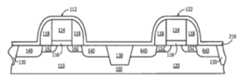
- a first active area 110 including a first insulated gate 112 thereon, and second active area 120 including a second insulated gate 122 thereonare formed on an integrated circuit substrate 100 .
- the integrated circuit substratemay be a single and/or compound semiconductor integrated circuit substrate including one or more layers thereon, and/or may be a semiconductor layer on a substrate.
- Example integrated circuit substrates 100can include monocrystalline silicon substrates or semiconductor-on-insulator substrates.
- the first active region 110may be used to form an n-channel field effect transistor (NFET) device, also referred to as an NMOS device, and the second active region 120 may be used to form a p-channel field effect transistor (PFET), also referred to as a PMOS device, so that the integrated circuit substrate may be used to form complementary insulated gate field effect transistors, also referred to as CMOS devices.
- NFETn-channel field effect transistor
- PMOSp-channel field effect transistor
- CMOS devicescomplementary insulated gate field effect transistors
- the first and second active regionsmay be insulated from one another by an insulating region 130 , such as a shallow trench isolation region and/or other insulating region well known to those having skill in the art.
- the first and second insulated gates 112 , 122may include a gate electrode 114 that may include one or more conductive layers, and an underlying gate insulating layer 116 that may also include one or more insulating layers.
- the gate electrodes 114 and/or the gate insulating layers 116may be the same or different for the first and second insulated gates 112 and 122 , respectively.
- a sidewall spacer 118also may be included on sidewalls of the first and second insulated gates 112 and 122 , respectively.
- the design of the first and second insulated gates 112 and 122 , respectively,are well known to those having skill in the art, and need not be described further herein.
- source/drain regions 140 and extension regions 142also may be formed on the first active region 110 , wherein the source/drain regions 140 are spaced apart from the first insulated gate 112 , and the extension regions 142 are provided between the insulated gate and the source/drain regions 140 .
- extension regions 152are formed, but source/drain regions are not formed. The design and fabrication of source/drain regions and extension regions are well known to those having skill in the art, and need not be described further herein.
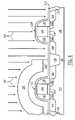
- an oxide layersuch as a silicon dioxide etch stop layer 210 , may be formed.
- the fabrication of an oxide etch stop layer 210is well known to those having skill in the art, and need not be described further herein.
- a nitride stress-generating layer 220 , a carbon-containing layer 230 , an etch stop layer 240 and a photoresist layerare blanket formed on both the first and second active areas, 110 and 120 , respectively.
- the photoresist layer 250is selectively removed from the etch stop layer 240 on the second active area 120 , to expose the etch stop layer 240 on the second active area 120 , while retaining at least some of the photoresist layer 250 on the etch stop layer on the first active area.
- the design and fabrication of nitride stress-generating layers 220are well known to those having skill in the art and need not be described further herein.
- the carbon-containing layer 230may be an amorphous carbon layer or an organic top-coating materials for photoresist, such as the NFC top-coating material marketed by Japan Synthetic Rubber (JSR).
- JSRJapan Synthetic Rubber
- the design and fabrication of amorphous carbon layers and organic top-coating materials for photoresistsare well known to those having skill in the art and need not be described further herein.
- the etch stop layer 240may be a low temperature oxide (LTO) and/or other etch stop layer well known to those having skill in the art.
- LTOlow temperature oxide
- the fabrication and patterning of the photoresist layer 250is well known to those having skill in the art and need not be described further herein.
- the etch stop layer 240 that is exposed on the second active area 120is removed, so that the etch stop layer 240 ′ remains on the first active area 110 .
- the photoresist layer 250 on the first active area 110is etched, to expose the remaining etch stop layer 240 ′ on the first active area 110 , while simultaneously etching the carbon-containing layer 230 on the second active area 120 , to expose the nitride stress-generating layer 220 on the second active area 120 .
- both the photoresist layer 250 and the carbon-containing layercontain carbon, a 1:1 etch may be formed on both layers using a conventional photoresist etchant, so that, in some embodiments, all of the photoresist layer 250 on the first active area 110 and all of the carbon-containing layer 230 on the second active area 120 may be removed simultaneously.
- the carbon-containing layer 230 ′ on the first active area 110remains.
- the stress-generating layer 220 on the second active areais covered by the carbon-containing layer 230 on the second active area 120 , so that contamination of the nitride stress-generating layer 220 on the second active area 120 during removal of the photoresist layer 250 may be reduced or prevented.
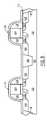
- the etch stop layer 240 ′ that is exposed on the first active area 110is removed, to expose the carbon-containing layer 230 ′ on the first active area.
- the nitride stress-generating layer 220 that is exposed on the second active area 120is removed, so that nitride stress-generating layer 220 ′ remains on the first active area 110 .
- the etching of the etch stop layer 240 ′ on the first active area 110 , and the etching of the nitride stress-generating layer 220 on the second active area 120may be performed simultaneously using a conventional etchant with a 1:5 etch ratio, in some embodiments.
- the operations of FIGS. 4 and 5may be performed using one continuous etching operation using conventional etchants.
- dopantssuch as germanium dopants 610
- dopants 610are implanted to the second active area 120 , to form source/drain regions 640 in the second active area 120 , while simultaneously blocking implantation of the dopants 610 into the nitride stress-generating layer 220 ′ on the first active area 110 by the carbon-containing layer 230 ′ on the first active area.
- the dopants 610may be implanted through the etch stop layer 210 . In other embodiments, the etch stop layer 210 may be removed.
- the carbon-containing layer 230 ′can reduce or prevent the dopants 610 from being implanted into, and potentially degrading, the nitride stress-generating layer 220 ′. It will also be understood that the implantation of dopants 610 is illustrated as being orthogonal to the substrate 100 . However, combinations of orthogonal and/or oblique implantations also may be performed using techniques well known to those having skill in the art.
- the remaining carbon-containing layer 230 ′ on the first active area 110is removed, and annealing is performed to memorize the stress in the first active area 110 that is generated by the nitride stress-generating layer 220 ′ on the first active area 110 .
- the nitride stress-generating layer 220 ′is removed from the first active area 110 , for example using a wet etch. Subsequent conventional processing steps may be performed, for example, to form silicide contacts and to perform additional conventional processing steps well known to those having skill in the art, to complete the transistors.
- the etch stop layer 240 of FIG. 2need not be used and the photoresist 250 on the active area 110 and the carbon-containing layer 230 on the second active area 120 may be etched simultaneously without the need for etch stop layer 240 .
- embodiments of the inventionthat have been described above can simultaneously remove a photoresist layer 250 on a first active area 110 of an integrated circuit substrate 100 , and a carbon-containing layer 230 on a second active area 120 of the integrated circuit substrate 100 , to expose a nitride stress-generating layer 220 on the second active area 120 , while reducing or eliminating contamination of the nitride stress-generating layer 220 on the second active area 120 .
- a single mask 250may be used to define the second active area 120 for removal of a nitride stress-generating layer 220 and for source/drain implants 640 in the second active area 120 , for example for a PFET. Accordingly, reduced process complexity and/or reduced contamination may be obtained.
Landscapes
- Metal-Oxide And Bipolar Metal-Oxide Semiconductor Integrated Circuits (AREA)
Abstract
Description
Claims (16)
Priority Applications (3)
| Application Number | Priority Date | Filing Date | Title |
|---|---|---|---|
| US11/266,024US7541234B2 (en) | 2005-11-03 | 2005-11-03 | Methods of fabricating integrated circuit transistors by simultaneously removing a photoresist layer and a carbon-containing layer on different active areas |
| SG200606453-9ASG131845A1 (en) | 2005-11-03 | 2006-09-15 | Methods of fabricating integrated circuit transistors by simultaneously removing a photoresist layer and a carbon-containing layer on different active areas |
| KR1020060099917AKR100791330B1 (en) | 2005-11-03 | 2006-10-13 | A method of forming an integrated circuit transistor that simultaneously removes a photoresist layer and a carbon containing layer on another active region |
Applications Claiming Priority (1)
| Application Number | Priority Date | Filing Date | Title |
|---|---|---|---|
| US11/266,024US7541234B2 (en) | 2005-11-03 | 2005-11-03 | Methods of fabricating integrated circuit transistors by simultaneously removing a photoresist layer and a carbon-containing layer on different active areas |
Publications (2)
| Publication Number | Publication Date |
|---|---|
| US20070099126A1 US20070099126A1 (en) | 2007-05-03 |
| US7541234B2true US7541234B2 (en) | 2009-06-02 |
Family
ID=37996810
Family Applications (1)
| Application Number | Title | Priority Date | Filing Date |
|---|---|---|---|
| US11/266,024Active2027-04-12US7541234B2 (en) | 2005-11-03 | 2005-11-03 | Methods of fabricating integrated circuit transistors by simultaneously removing a photoresist layer and a carbon-containing layer on different active areas |
Country Status (3)
| Country | Link |
|---|---|
| US (1) | US7541234B2 (en) |
| KR (1) | KR100791330B1 (en) |
| SG (1) | SG131845A1 (en) |
Families Citing this family (4)
| Publication number | Priority date | Publication date | Assignee | Title |
|---|---|---|---|---|
| US20080179638A1 (en)* | 2007-01-31 | 2008-07-31 | International Business Machines Corporation | Gap fill for underlapped dual stress liners |
| KR100839359B1 (en)* | 2007-05-10 | 2008-06-19 | 삼성전자주식회사 | PMOS transistor manufacturing method and complementary MOS transistor manufacturing method |
| KR20090061162A (en)* | 2007-12-11 | 2009-06-16 | 주식회사 동부하이텍 | Method for manufacturing a semicondoctor device |
| CN111933642A (en)* | 2020-09-18 | 2020-11-13 | 晶芯成(北京)科技有限公司 | Semiconductor device and manufacturing method thereof |
Citations (40)
| Publication number | Priority date | Publication date | Assignee | Title |
|---|---|---|---|---|
| US4382827A (en) | 1981-04-27 | 1983-05-10 | Ncr Corporation | Silicon nitride S/D ion implant mask in CMOS device fabrication |
| US5024959A (en) | 1989-09-25 | 1991-06-18 | Motorola, Inc. | CMOS process using doped glass layer |
| US5439834A (en) | 1994-11-15 | 1995-08-08 | Winbond Electronics Corp. | Method for fabricating a CMOS device with reduced number of photolithography steps |
| KR950011781B1 (en) | 1986-04-08 | 1995-10-10 | 지멘스 악티엔게젤샤프트 | Manufacturing Method of Optimal CM0S-FET Using VLSI Technology |
| US5460998A (en) | 1995-03-17 | 1995-10-24 | Taiwan Semiconductor Manufacturing Company | Integrated P+ implant sequence in DPDM process for suppression of GIDL |
| US5620919A (en)* | 1990-01-12 | 1997-04-15 | Paradigm Technology, Inc. | Methods for fabricating integrated circuits including openings to transistor regions |
| US5766991A (en) | 1990-05-11 | 1998-06-16 | U.S. Philips Corporation | CMOS process utilizing disposable silicon nitride spacers for making lightly doped drain |
| JPH10256390A (en) | 1997-03-06 | 1998-09-25 | Yamaha Corp | Manufacture of semiconductor device |
| US5936300A (en)* | 1996-03-25 | 1999-08-10 | Sanyo Electric Co., Ltd. | Semiconductor device with film covering |
| KR100247478B1 (en) | 1997-09-29 | 2000-03-15 | 김영환 | CMOS transistor manufacturing method |
| US20010001718A1 (en)* | 1996-01-17 | 2001-05-24 | Kenichi Kikushima | Semiconductor integrated circuit device and method of manufacture thereof |
| US6359276B1 (en)* | 1998-10-21 | 2002-03-19 | Xiang Zheng Tu | Microbolom infrared sensors |
| KR20020054898A (en) | 2000-12-28 | 2002-07-08 | 박종섭 | Method of manufacturing transistor cmos |
| US6475888B1 (en)* | 2001-04-30 | 2002-11-05 | Hynix Semiconductor Inc. | Method for forming ultra-shallow junctions using laser annealing |
| US20030040158A1 (en)* | 2001-08-21 | 2003-02-27 | Nec Corporation | Semiconductor device and method of fabricating the same |
| US6573172B1 (en)* | 2002-09-16 | 2003-06-03 | Advanced Micro Devices, Inc. | Methods for improving carrier mobility of PMOS and NMOS devices |
| US20030181005A1 (en)* | 2002-03-19 | 2003-09-25 | Kiyota Hachimine | Semiconductor device and a method of manufacturing the same |
| US20040029323A1 (en) | 2000-11-22 | 2004-02-12 | Akihiro Shimizu | Semiconductor device and method for fabricating the same |
| US20040104405A1 (en)* | 2002-12-02 | 2004-06-03 | Taiwan Semiconductor Manufacturing Company | Novel CMOS device |
| KR20040057519A (en) | 2002-12-26 | 2004-07-02 | 주식회사 하이닉스반도체 | Method for manufacturing a semiconductor device |
| US20040180483A1 (en) | 2003-03-10 | 2004-09-16 | Samsung Electronics Co., Ltd. | Method of manufacturing CMOS transistor with LDD structure |
| US20040180504A1 (en) | 2003-03-12 | 2004-09-16 | Samsung Electronics Co., Ltd. | Method of manufacturing a MOS transistor of a semiconductor device |
| KR20040102656A (en) | 2003-05-28 | 2004-12-08 | 삼성전자주식회사 | method of fabricating Source/Drain Extension structure type CMOS |
| US20050020022A1 (en)* | 2003-07-21 | 2005-01-27 | Grudowski Paul A. | Transistor sidewall spacer stress modulation |
| US20050069816A1 (en) | 1999-06-03 | 2005-03-31 | Hynix Semiconductor Inc. | Process for forming a fine pattern using a top-coating composition for a photoresist and product formed by same |
| US20050194596A1 (en)* | 2003-10-30 | 2005-09-08 | Victor Chan | Increasing carrier mobility in NFET and PFET transistors on a common wafer |
| US20050214998A1 (en)* | 2004-03-26 | 2005-09-29 | Taiwan Semiconductor Manufacturing Co., Ltd. | Local stress control for CMOS performance enhancement |
| US20050230756A1 (en)* | 2004-04-15 | 2005-10-20 | Sun-Jay Chang | CMOS device and method of manufacture |
| US20060128086A1 (en)* | 2004-12-10 | 2006-06-15 | International Business Machines Corporation | Device having dual etch stop liner and protective layer and related methods |
| US20060228848A1 (en)* | 2005-03-31 | 2006-10-12 | International Business Machines Corporation | Dual-hybrid liner formation without exposing silicide layer to photoresist stripping chemicals |
| US20070048907A1 (en)* | 2005-08-24 | 2007-03-01 | Ho Lee | Methods of forming NMOS/PMOS transistors with source/drains including strained materials and devices so formed |
| US7193254B2 (en)* | 2004-11-30 | 2007-03-20 | International Business Machines Corporation | Structure and method of applying stresses to PFET and NFET transistor channels for improved performance |
| US20070077708A1 (en)* | 2005-09-30 | 2007-04-05 | Kai Frohberg | Technique for creating different mechanical strain by forming a contact etch stop layer stack having differently modified intrinsic stress |
| US7214629B1 (en)* | 2004-11-16 | 2007-05-08 | Xilinx, Inc. | Strain-silicon CMOS with dual-stressed film |
| US7220630B2 (en)* | 2004-05-21 | 2007-05-22 | Taiwan Semiconductor Manufacturing Co., Ltd. | Method for selectively forming strained etch stop layers to improve FET charge carrier mobility |
| US7244644B2 (en)* | 2005-07-21 | 2007-07-17 | International Business Machines Corporation | Undercut and residual spacer prevention for dual stressed layers |
| US7288451B2 (en)* | 2005-03-01 | 2007-10-30 | International Business Machines Corporation | Method and structure for forming self-aligned, dual stress liner for CMOS devices |
| US7309637B2 (en)* | 2005-12-12 | 2007-12-18 | Chartered Semiconductor Manufacturing, Ltd | Method to enhance device performance with selective stress relief |
| US7314836B2 (en)* | 2004-06-30 | 2008-01-01 | Intel Corporation | Enhanced nitride layers for metal oxide semiconductors |
| US7374987B2 (en)* | 2002-12-12 | 2008-05-20 | International Business Machines Corporation | Stress inducing spacers |
- 2005
- 2005-11-03USUS11/266,024patent/US7541234B2/enactiveActive
- 2006
- 2006-09-15SGSG200606453-9Apatent/SG131845A1/enunknown
- 2006-10-13KRKR1020060099917Apatent/KR100791330B1/enactiveActive
Patent Citations (48)
| Publication number | Priority date | Publication date | Assignee | Title |
|---|---|---|---|---|
| US4382827A (en) | 1981-04-27 | 1983-05-10 | Ncr Corporation | Silicon nitride S/D ion implant mask in CMOS device fabrication |
| KR950011781B1 (en) | 1986-04-08 | 1995-10-10 | 지멘스 악티엔게젤샤프트 | Manufacturing Method of Optimal CM0S-FET Using VLSI Technology |
| US5024959A (en) | 1989-09-25 | 1991-06-18 | Motorola, Inc. | CMOS process using doped glass layer |
| US5620919A (en)* | 1990-01-12 | 1997-04-15 | Paradigm Technology, Inc. | Methods for fabricating integrated circuits including openings to transistor regions |
| US5766991A (en) | 1990-05-11 | 1998-06-16 | U.S. Philips Corporation | CMOS process utilizing disposable silicon nitride spacers for making lightly doped drain |
| US5439834A (en) | 1994-11-15 | 1995-08-08 | Winbond Electronics Corp. | Method for fabricating a CMOS device with reduced number of photolithography steps |
| US5460998A (en) | 1995-03-17 | 1995-10-24 | Taiwan Semiconductor Manufacturing Company | Integrated P+ implant sequence in DPDM process for suppression of GIDL |
| US20010001718A1 (en)* | 1996-01-17 | 2001-05-24 | Kenichi Kikushima | Semiconductor integrated circuit device and method of manufacture thereof |
| US5936300A (en)* | 1996-03-25 | 1999-08-10 | Sanyo Electric Co., Ltd. | Semiconductor device with film covering |
| JPH10256390A (en) | 1997-03-06 | 1998-09-25 | Yamaha Corp | Manufacture of semiconductor device |
| KR100247478B1 (en) | 1997-09-29 | 2000-03-15 | 김영환 | CMOS transistor manufacturing method |
| US6359276B1 (en)* | 1998-10-21 | 2002-03-19 | Xiang Zheng Tu | Microbolom infrared sensors |
| US20050069816A1 (en) | 1999-06-03 | 2005-03-31 | Hynix Semiconductor Inc. | Process for forming a fine pattern using a top-coating composition for a photoresist and product formed by same |
| US20040029323A1 (en) | 2000-11-22 | 2004-02-12 | Akihiro Shimizu | Semiconductor device and method for fabricating the same |
| US7115954B2 (en)* | 2000-11-22 | 2006-10-03 | Renesas Technology Corp. | Semiconductor device including stress inducing films formed over n-channel and p-channel field effect transistors and a method of manufacturing the same |
| KR20020054898A (en) | 2000-12-28 | 2002-07-08 | 박종섭 | Method of manufacturing transistor cmos |
| US6475888B1 (en)* | 2001-04-30 | 2002-11-05 | Hynix Semiconductor Inc. | Method for forming ultra-shallow junctions using laser annealing |
| JP2003060076A (en) | 2001-08-21 | 2003-02-28 | Nec Corp | Semiconductor device and manufacturing method thereof |
| US20030040158A1 (en)* | 2001-08-21 | 2003-02-27 | Nec Corporation | Semiconductor device and method of fabricating the same |
| US20030181005A1 (en)* | 2002-03-19 | 2003-09-25 | Kiyota Hachimine | Semiconductor device and a method of manufacturing the same |
| US6573172B1 (en)* | 2002-09-16 | 2003-06-03 | Advanced Micro Devices, Inc. | Methods for improving carrier mobility of PMOS and NMOS devices |
| US20040104405A1 (en)* | 2002-12-02 | 2004-06-03 | Taiwan Semiconductor Manufacturing Company | Novel CMOS device |
| US7022561B2 (en)* | 2002-12-02 | 2006-04-04 | Taiwan Semiconductor Manufacturing Company, Ltd. | CMOS device |
| US7374987B2 (en)* | 2002-12-12 | 2008-05-20 | International Business Machines Corporation | Stress inducing spacers |
| KR20040057519A (en) | 2002-12-26 | 2004-07-02 | 주식회사 하이닉스반도체 | Method for manufacturing a semiconductor device |
| KR20040079747A (en) | 2003-03-10 | 2004-09-16 | 삼성전자주식회사 | Method for manufacturing CMOS transistor having lightly doped drain structure |
| US20040180483A1 (en) | 2003-03-10 | 2004-09-16 | Samsung Electronics Co., Ltd. | Method of manufacturing CMOS transistor with LDD structure |
| KR20040080510A (en) | 2003-03-12 | 2004-09-20 | 삼성전자주식회사 | Method for manufacturing a MOS transistor in semiconductor device |
| US20040180504A1 (en) | 2003-03-12 | 2004-09-16 | Samsung Electronics Co., Ltd. | Method of manufacturing a MOS transistor of a semiconductor device |
| JP2004282068A (en) | 2003-03-12 | 2004-10-07 | Samsung Electronics Co Ltd | Method for forming semiconductor device |
| KR20040102656A (en) | 2003-05-28 | 2004-12-08 | 삼성전자주식회사 | method of fabricating Source/Drain Extension structure type CMOS |
| US20050020022A1 (en)* | 2003-07-21 | 2005-01-27 | Grudowski Paul A. | Transistor sidewall spacer stress modulation |
| US20050194596A1 (en)* | 2003-10-30 | 2005-09-08 | Victor Chan | Increasing carrier mobility in NFET and PFET transistors on a common wafer |
| US7211869B2 (en)* | 2003-10-30 | 2007-05-01 | International Business Machines Corporation | Increasing carrier mobility in NFET and PFET transistors on a common wafer |
| US20050214998A1 (en)* | 2004-03-26 | 2005-09-29 | Taiwan Semiconductor Manufacturing Co., Ltd. | Local stress control for CMOS performance enhancement |
| US20050230756A1 (en)* | 2004-04-15 | 2005-10-20 | Sun-Jay Chang | CMOS device and method of manufacture |
| US7190033B2 (en)* | 2004-04-15 | 2007-03-13 | Taiwan Semiconductor Manufacturing Company, Ltd. | CMOS device and method of manufacture |
| US7220630B2 (en)* | 2004-05-21 | 2007-05-22 | Taiwan Semiconductor Manufacturing Co., Ltd. | Method for selectively forming strained etch stop layers to improve FET charge carrier mobility |
| US7314836B2 (en)* | 2004-06-30 | 2008-01-01 | Intel Corporation | Enhanced nitride layers for metal oxide semiconductors |
| US7214629B1 (en)* | 2004-11-16 | 2007-05-08 | Xilinx, Inc. | Strain-silicon CMOS with dual-stressed film |
| US7193254B2 (en)* | 2004-11-30 | 2007-03-20 | International Business Machines Corporation | Structure and method of applying stresses to PFET and NFET transistor channels for improved performance |
| US20060128086A1 (en)* | 2004-12-10 | 2006-06-15 | International Business Machines Corporation | Device having dual etch stop liner and protective layer and related methods |
| US7288451B2 (en)* | 2005-03-01 | 2007-10-30 | International Business Machines Corporation | Method and structure for forming self-aligned, dual stress liner for CMOS devices |
| US20060228848A1 (en)* | 2005-03-31 | 2006-10-12 | International Business Machines Corporation | Dual-hybrid liner formation without exposing silicide layer to photoresist stripping chemicals |
| US7244644B2 (en)* | 2005-07-21 | 2007-07-17 | International Business Machines Corporation | Undercut and residual spacer prevention for dual stressed layers |
| US20070048907A1 (en)* | 2005-08-24 | 2007-03-01 | Ho Lee | Methods of forming NMOS/PMOS transistors with source/drains including strained materials and devices so formed |
| US20070077708A1 (en)* | 2005-09-30 | 2007-04-05 | Kai Frohberg | Technique for creating different mechanical strain by forming a contact etch stop layer stack having differently modified intrinsic stress |
| US7309637B2 (en)* | 2005-12-12 | 2007-12-18 | Chartered Semiconductor Manufacturing, Ltd | Method to enhance device performance with selective stress relief |
Non-Patent Citations (2)
| Title |
|---|
| JSR Micro Materials Innovation, "Tarc Resists", downloaded on Sep. 17, 2005 from http://www.jsrmicro.com/pro-photo-Tarc.html. |
| Notice of Allowance, KR 10-2006-0099917, Nov. 29, 2007. |
Also Published As
| Publication number | Publication date |
|---|---|
| SG131845A1 (en) | 2007-05-28 |
| KR20070048116A (en) | 2007-05-08 |
| KR100791330B1 (en) | 2008-01-03 |
| US20070099126A1 (en) | 2007-05-03 |
Similar Documents
| Publication | Publication Date | Title |
|---|---|---|
| US7354806B2 (en) | Semiconductor device structure with active regions having different surface directions and methods | |
| US7820518B2 (en) | Transistor fabrication methods and structures thereof | |
| US8119541B2 (en) | Modulation of stress in stress film through ion implantation and its application in stress memorization technique | |
| US7098477B2 (en) | Structure and method of manufacturing a finFET device having stacked fins | |
| US20110031555A1 (en) | Metal oxide semiconductor transistor | |
| US20110049630A1 (en) | Stressed Source/Drain CMOS and Method of Forming Same | |
| US7432167B2 (en) | Method of fabricating a strained silicon channel metal oxide semiconductor transistor | |
| EP1026738B1 (en) | Novel mixed voltage CMOS process for high reliability and high performance core and I/O transistors with reduced mask steps | |
| US20010048136A1 (en) | Fabrication of low power CMOS device with high reliability | |
| US6908800B1 (en) | Tunable sidewall spacer process for CMOS integrated circuits | |
| US9224655B2 (en) | Methods of removing gate cap layers in CMOS applications | |
| US7541234B2 (en) | Methods of fabricating integrated circuit transistors by simultaneously removing a photoresist layer and a carbon-containing layer on different active areas | |
| US20040180483A1 (en) | Method of manufacturing CMOS transistor with LDD structure | |
| US20080233695A1 (en) | Integration method of inversion oxide (TOXinv) thickness reduction in CMOS flow without added pattern | |
| US20090065806A1 (en) | Mos transistor and fabrication method thereof | |
| US6855590B2 (en) | Method of manufacturing the semiconductor device intended to prevent a leakage current from occuring due to a gate induced drain leakage effect | |
| US7307320B2 (en) | Differential mechanical stress-producing regions for integrated circuit field effect transistors | |
| US7351627B2 (en) | Method of manufacturing semiconductor device using gate-through ion implantation | |
| US6541359B1 (en) | Optimized gate implants for reducing dopant effects during gate etching | |
| US7585763B2 (en) | Methods of fabricating integrated circuit devices using anti-reflective coating as implant blocking layer | |
| TW200845233A (en) | Method of manufacturing a semiconductor device and semiconductor device | |
| CN119170572A (en) | Semiconductor structure manufacturing method, semiconductor structure and CMOS circuit | |
| KR20030050780A (en) | Method of manufacturing a transistor in a semiconductor device | |
| KR20010057471A (en) | method for fabricating CMOS transistor | |
| KR20040056449A (en) | Method of manufacturing a transistor in a semiconductor device |
Legal Events
| Date | Code | Title | Description |
|---|---|---|---|
| AS | Assignment | Owner name:SAMSUNG ELECTRONICS CO., LTD., KOREA, REPUBLIC OF Free format text:ASSIGNMENT OF ASSIGNORS INTEREST;ASSIGNORS:CHANG, CHONG KWANG;KO, YOUNG GUN;REEL/FRAME:017189/0916 Effective date:20051027 | |
| AS | Assignment | Owner name:CHARTERED SEMICONDUCTOR MANUFACTURING LTD., SINGAP Free format text:ASSIGNMENT OF ASSIGNORS INTEREST;ASSIGNORS:MISHRA, SHAILENDRA;TJOA, TJIN TJIN;REEL/FRAME:017212/0495;SIGNING DATES FROM 20060117 TO 20060118 | |
| AS | Assignment | Owner name:INFINEON TECHNOLOGIES NORTH AMERICA CORP., CALIFOR Free format text:ASSIGNMENT OF ASSIGNORS INTEREST;ASSIGNORS:KWON, O SUNG;LIPINSKI, MATTHIAS;ZHUANG, HAOREN;REEL/FRAME:017528/0325;SIGNING DATES FROM 20060419 TO 20060424 | |
| AS | Assignment | Owner name:INFINEON TECHNOLOGIES AG, GERMANY Free format text:ASSIGNMENT OF ASSIGNORS INTEREST;ASSIGNOR:INFINEON TECHNOLOGIES NORTH AMERICA CORP.;REEL/FRAME:017535/0508 Effective date:20060427 | |
| FEPP | Fee payment procedure | Free format text:PAYOR NUMBER ASSIGNED (ORIGINAL EVENT CODE: ASPN); ENTITY STATUS OF PATENT OWNER: LARGE ENTITY | |
| STCF | Information on status: patent grant | Free format text:PATENTED CASE | |
| FPAY | Fee payment | Year of fee payment:4 | |
| FPAY | Fee payment | Year of fee payment:8 | |
| MAFP | Maintenance fee payment | Free format text:PAYMENT OF MAINTENANCE FEE, 12TH YEAR, LARGE ENTITY (ORIGINAL EVENT CODE: M1553); ENTITY STATUS OF PATENT OWNER: LARGE ENTITY Year of fee payment:12 |