US7540899B1 - Shape memory alloy thin film, method of fabrication, and articles of manufacture - Google Patents
Shape memory alloy thin film, method of fabrication, and articles of manufactureDownload PDFInfo
- Publication number
- US7540899B1 US7540899B1US11/420,157US42015706AUS7540899B1US 7540899 B1US7540899 B1US 7540899B1US 42015706 AUS42015706 AUS 42015706AUS 7540899 B1US7540899 B1US 7540899B1
- Authority
- US
- United States
- Prior art keywords
- shape memory
- thin film
- memory alloy
- single crystal
- heat
- Prior art date
- Legal status (The legal status is an assumption and is not a legal conclusion. Google has not performed a legal analysis and makes no representation as to the accuracy of the status listed.)
- Active, expires
Links
Images


Classifications
- C—CHEMISTRY; METALLURGY
- C30—CRYSTAL GROWTH
- C30B—SINGLE-CRYSTAL GROWTH; UNIDIRECTIONAL SOLIDIFICATION OF EUTECTIC MATERIAL OR UNIDIRECTIONAL DEMIXING OF EUTECTOID MATERIAL; REFINING BY ZONE-MELTING OF MATERIAL; PRODUCTION OF A HOMOGENEOUS POLYCRYSTALLINE MATERIAL WITH DEFINED STRUCTURE; SINGLE CRYSTALS OR HOMOGENEOUS POLYCRYSTALLINE MATERIAL WITH DEFINED STRUCTURE; AFTER-TREATMENT OF SINGLE CRYSTALS OR A HOMOGENEOUS POLYCRYSTALLINE MATERIAL WITH DEFINED STRUCTURE; APPARATUS THEREFOR
- C30B1/00—Single-crystal growth directly from the solid state
- C30B1/02—Single-crystal growth directly from the solid state by thermal treatment, e.g. strain annealing
- C30B1/023—Single-crystal growth directly from the solid state by thermal treatment, e.g. strain annealing from solids with amorphous structure
- A—HUMAN NECESSITIES
- A61—MEDICAL OR VETERINARY SCIENCE; HYGIENE
- A61L—METHODS OR APPARATUS FOR STERILISING MATERIALS OR OBJECTS IN GENERAL; DISINFECTION, STERILISATION OR DEODORISATION OF AIR; CHEMICAL ASPECTS OF BANDAGES, DRESSINGS, ABSORBENT PADS OR SURGICAL ARTICLES; MATERIALS FOR BANDAGES, DRESSINGS, ABSORBENT PADS OR SURGICAL ARTICLES
- A61L27/00—Materials for grafts or prostheses or for coating grafts or prostheses
- A61L27/02—Inorganic materials
- A61L27/04—Metals or alloys
- A—HUMAN NECESSITIES
- A61—MEDICAL OR VETERINARY SCIENCE; HYGIENE
- A61L—METHODS OR APPARATUS FOR STERILISING MATERIALS OR OBJECTS IN GENERAL; DISINFECTION, STERILISATION OR DEODORISATION OF AIR; CHEMICAL ASPECTS OF BANDAGES, DRESSINGS, ABSORBENT PADS OR SURGICAL ARTICLES; MATERIALS FOR BANDAGES, DRESSINGS, ABSORBENT PADS OR SURGICAL ARTICLES
- A61L27/00—Materials for grafts or prostheses or for coating grafts or prostheses
- A61L27/50—Materials characterised by their function or physical properties, e.g. injectable or lubricating compositions, shape-memory materials, surface modified materials
- A—HUMAN NECESSITIES
- A61—MEDICAL OR VETERINARY SCIENCE; HYGIENE
- A61L—METHODS OR APPARATUS FOR STERILISING MATERIALS OR OBJECTS IN GENERAL; DISINFECTION, STERILISATION OR DEODORISATION OF AIR; CHEMICAL ASPECTS OF BANDAGES, DRESSINGS, ABSORBENT PADS OR SURGICAL ARTICLES; MATERIALS FOR BANDAGES, DRESSINGS, ABSORBENT PADS OR SURGICAL ARTICLES
- A61L31/00—Materials for other surgical articles, e.g. stents, stent-grafts, shunts, surgical drapes, guide wires, materials for adhesion prevention, occluding devices, surgical gloves, tissue fixation devices
- A61L31/02—Inorganic materials
- A61L31/022—Metals or alloys
- A—HUMAN NECESSITIES
- A61—MEDICAL OR VETERINARY SCIENCE; HYGIENE
- A61L—METHODS OR APPARATUS FOR STERILISING MATERIALS OR OBJECTS IN GENERAL; DISINFECTION, STERILISATION OR DEODORISATION OF AIR; CHEMICAL ASPECTS OF BANDAGES, DRESSINGS, ABSORBENT PADS OR SURGICAL ARTICLES; MATERIALS FOR BANDAGES, DRESSINGS, ABSORBENT PADS OR SURGICAL ARTICLES
- A61L31/00—Materials for other surgical articles, e.g. stents, stent-grafts, shunts, surgical drapes, guide wires, materials for adhesion prevention, occluding devices, surgical gloves, tissue fixation devices
- A61L31/14—Materials characterised by their function or physical properties, e.g. injectable or lubricating compositions, shape-memory materials, surface modified materials
- C—CHEMISTRY; METALLURGY
- C22—METALLURGY; FERROUS OR NON-FERROUS ALLOYS; TREATMENT OF ALLOYS OR NON-FERROUS METALS
- C22C—ALLOYS
- C22C1/00—Making non-ferrous alloys
- C22C1/11—Making amorphous alloys
- C—CHEMISTRY; METALLURGY
- C22—METALLURGY; FERROUS OR NON-FERROUS ALLOYS; TREATMENT OF ALLOYS OR NON-FERROUS METALS
- C22C—ALLOYS
- C22C14/00—Alloys based on titanium
- C—CHEMISTRY; METALLURGY
- C22—METALLURGY; FERROUS OR NON-FERROUS ALLOYS; TREATMENT OF ALLOYS OR NON-FERROUS METALS
- C22C—ALLOYS
- C22C19/00—Alloys based on nickel or cobalt
- C22C19/03—Alloys based on nickel or cobalt based on nickel
- C—CHEMISTRY; METALLURGY
- C23—COATING METALLIC MATERIAL; COATING MATERIAL WITH METALLIC MATERIAL; CHEMICAL SURFACE TREATMENT; DIFFUSION TREATMENT OF METALLIC MATERIAL; COATING BY VACUUM EVAPORATION, BY SPUTTERING, BY ION IMPLANTATION OR BY CHEMICAL VAPOUR DEPOSITION, IN GENERAL; INHIBITING CORROSION OF METALLIC MATERIAL OR INCRUSTATION IN GENERAL
- C23C—COATING METALLIC MATERIAL; COATING MATERIAL WITH METALLIC MATERIAL; SURFACE TREATMENT OF METALLIC MATERIAL BY DIFFUSION INTO THE SURFACE, BY CHEMICAL CONVERSION OR SUBSTITUTION; COATING BY VACUUM EVAPORATION, BY SPUTTERING, BY ION IMPLANTATION OR BY CHEMICAL VAPOUR DEPOSITION, IN GENERAL
- C23C14/00—Coating by vacuum evaporation, by sputtering or by ion implantation of the coating forming material
- C23C14/06—Coating by vacuum evaporation, by sputtering or by ion implantation of the coating forming material characterised by the coating material
- C23C14/14—Metallic material, boron or silicon
- C23C14/16—Metallic material, boron or silicon on metallic substrates or on substrates of boron or silicon
- C23C14/165—Metallic material, boron or silicon on metallic substrates or on substrates of boron or silicon by cathodic sputtering
- C—CHEMISTRY; METALLURGY
- C23—COATING METALLIC MATERIAL; COATING MATERIAL WITH METALLIC MATERIAL; CHEMICAL SURFACE TREATMENT; DIFFUSION TREATMENT OF METALLIC MATERIAL; COATING BY VACUUM EVAPORATION, BY SPUTTERING, BY ION IMPLANTATION OR BY CHEMICAL VAPOUR DEPOSITION, IN GENERAL; INHIBITING CORROSION OF METALLIC MATERIAL OR INCRUSTATION IN GENERAL
- C23C—COATING METALLIC MATERIAL; COATING MATERIAL WITH METALLIC MATERIAL; SURFACE TREATMENT OF METALLIC MATERIAL BY DIFFUSION INTO THE SURFACE, BY CHEMICAL CONVERSION OR SUBSTITUTION; COATING BY VACUUM EVAPORATION, BY SPUTTERING, BY ION IMPLANTATION OR BY CHEMICAL VAPOUR DEPOSITION, IN GENERAL
- C23C14/00—Coating by vacuum evaporation, by sputtering or by ion implantation of the coating forming material
- C23C14/22—Coating by vacuum evaporation, by sputtering or by ion implantation of the coating forming material characterised by the process of coating
- C23C14/34—Sputtering
- C—CHEMISTRY; METALLURGY
- C23—COATING METALLIC MATERIAL; COATING MATERIAL WITH METALLIC MATERIAL; CHEMICAL SURFACE TREATMENT; DIFFUSION TREATMENT OF METALLIC MATERIAL; COATING BY VACUUM EVAPORATION, BY SPUTTERING, BY ION IMPLANTATION OR BY CHEMICAL VAPOUR DEPOSITION, IN GENERAL; INHIBITING CORROSION OF METALLIC MATERIAL OR INCRUSTATION IN GENERAL
- C23C—COATING METALLIC MATERIAL; COATING MATERIAL WITH METALLIC MATERIAL; SURFACE TREATMENT OF METALLIC MATERIAL BY DIFFUSION INTO THE SURFACE, BY CHEMICAL CONVERSION OR SUBSTITUTION; COATING BY VACUUM EVAPORATION, BY SPUTTERING, BY ION IMPLANTATION OR BY CHEMICAL VAPOUR DEPOSITION, IN GENERAL
- C23C14/00—Coating by vacuum evaporation, by sputtering or by ion implantation of the coating forming material
- C23C14/58—After-treatment
- C23C14/5806—Thermal treatment
- C—CHEMISTRY; METALLURGY
- C30—CRYSTAL GROWTH
- C30B—SINGLE-CRYSTAL GROWTH; UNIDIRECTIONAL SOLIDIFICATION OF EUTECTIC MATERIAL OR UNIDIRECTIONAL DEMIXING OF EUTECTOID MATERIAL; REFINING BY ZONE-MELTING OF MATERIAL; PRODUCTION OF A HOMOGENEOUS POLYCRYSTALLINE MATERIAL WITH DEFINED STRUCTURE; SINGLE CRYSTALS OR HOMOGENEOUS POLYCRYSTALLINE MATERIAL WITH DEFINED STRUCTURE; AFTER-TREATMENT OF SINGLE CRYSTALS OR A HOMOGENEOUS POLYCRYSTALLINE MATERIAL WITH DEFINED STRUCTURE; APPARATUS THEREFOR
- C30B29/00—Single crystals or homogeneous polycrystalline material with defined structure characterised by the material or by their shape
- C30B29/10—Inorganic compounds or compositions
- C30B29/52—Alloys
- A—HUMAN NECESSITIES
- A61—MEDICAL OR VETERINARY SCIENCE; HYGIENE
- A61L—METHODS OR APPARATUS FOR STERILISING MATERIALS OR OBJECTS IN GENERAL; DISINFECTION, STERILISATION OR DEODORISATION OF AIR; CHEMICAL ASPECTS OF BANDAGES, DRESSINGS, ABSORBENT PADS OR SURGICAL ARTICLES; MATERIALS FOR BANDAGES, DRESSINGS, ABSORBENT PADS OR SURGICAL ARTICLES
- A61L2400/00—Materials characterised by their function or physical properties
- A61L2400/16—Materials with shape-memory or superelastic properties
- C—CHEMISTRY; METALLURGY
- C21—METALLURGY OF IRON
- C21D—MODIFYING THE PHYSICAL STRUCTURE OF FERROUS METALS; GENERAL DEVICES FOR HEAT TREATMENT OF FERROUS OR NON-FERROUS METALS OR ALLOYS; MAKING METAL MALLEABLE, e.g. BY DECARBURISATION OR TEMPERING
- C21D2201/00—Treatment for obtaining particular effects
- C21D2201/01—Shape memory effect
- C—CHEMISTRY; METALLURGY
- C22—METALLURGY; FERROUS OR NON-FERROUS ALLOYS; TREATMENT OF ALLOYS OR NON-FERROUS METALS
- C22B—PRODUCTION AND REFINING OF METALS; PRETREATMENT OF RAW MATERIALS
- C22B9/00—General processes of refining or remelting of metals; Apparatus for electroslag or arc remelting of metals
- C22B9/16—Remelting metals
- C22B9/22—Remelting metals with heating by wave energy or particle radiation
- C22B9/221—Remelting metals with heating by wave energy or particle radiation by electromagnetic waves, e.g. by gas discharge lamps
- C22B9/223—Remelting metals with heating by wave energy or particle radiation by electromagnetic waves, e.g. by gas discharge lamps by laser beams
Definitions
- the present inventionrelates to shape memory alloys (SMA), and more particularly to thin film superelastic single-crystal shape memory alloys (single crystal SMA or SCSMA) and multiple crystal SMA.
- Nitinol or NiTi or TiNiis an alloy of titanium nickel that undergoes an energetic crystalline phase change at near-ambient temperatures: these different phases have distinctly different mechanical characteristics giving rise to a shape change and accompanied by superelasticity.
- the superelastic properties of SMAare discussed in Shape Memory Materials, K Otsuka et al. eds. (Cambridge University Press 1998), pp. 27 et seq.
- TiNishape memory alloy
- Thin film SMAhas been made in laboratory quantities since 1989. Both bulk and thin film forms are polycrystalline.
- Single crystal SMAhaving a martensitic phase transformation, has much greater superelasticity than polycrystalline SMA.
- Some SMAssuch as Cu—Al—Ni can be made in single crystal form as they are pulled from melt and quenched. These crystals are not limited in length except for the capacity of the machine. TiNi is difficult to grow in this way, and single crystals are generally only a fraction of a centimeter long.
- Thin film TiNiis formed by vacuum sputter deposition.
- a process of crystallizationconsists of heating to near 500 degrees C., at which temperature many small crystals originate and coalesce into a crystalline form which has the shape memory property.
- Single crystals of bulk materialare formed by pulling molten material by surface tension to produce a moving crystallization front that progresses through the crystal as it is pulled.
- the Czochralski method for Silicon and Stepanov method for alloysare examples. These processes work by transforming the molten material (alloy or silicon) from a completely un-structured atomic arrangement to one that is completely ordered as it solidifies. Since in the initial state there are no grain boundaries to interfere with growth of the crystal, it grows as a single crystal in a preferred direction (with a crystallographic index value of ⁇ 100> for Cu—Al—Ni).
- Thin films of alloys, particularly TiNi,are formed as an amorphous layer which has no atomic order. Heating to an elevated temperature (490-520 degree C. for TiNi) allows crystals to form and to grow. When heating is uniform, especially if heating (and cooling) is slow, many nano-crystals form and grow simultaneously. However, by analogy with crystals pulled from melt, if a narrow crystallization front is moved through the thin film expanse by a process that rapidly heats and cools the material, it may be expected to crystallize along a preferred direction and form a single crystal in the same manner as a material pulled from melt.
- Another method of forming a single crystal thin filmis by use of a substrate with appropriate lattice parameters to grow a crystal epitaxially.
- the vertical structurewill permit larger deformations in the vertical direction and may be appropriate for nano memory applications.
- Nitinol materialsare used in numerous applications.
- Superelastic eyeglass frames and componentshave been known for years, and they are a major selling item in eyeglass manufacturing and retail. Such materials are polycrystalline, and hence the maximum recoverable strain is not achieved because not all crystal domains are oriented in a favorable direction.
- Superelastic Nitinolis also used in intravascular medical intervention.
- An aspect of this inventionprovides for creating a thin film of amorphous material that is a single crystal rather than polycrystalline form, by controlling the microstructure formation during crystal growth. From this process, oriented crystals with no grain boundaries evolve. The single crystal can be described as textured because the thinness of the film results in an apparent loss of some of the crystal variants.
- a method for fabricating a single crystal thin filmcomprising the steps of rapidly heating a shape memory alloy material to crystallization temperature with a simultaneous scanning motion so that a crystallization front or line moves or sweeps across the span of the film. Ahead of the front the material is amorphous. In the region of the front the material is hot enough to propagate a single crystal or a plurality of parallel crystals. Behind the crystallization front the material is a single crystal with a single crystal orientation.
- the inventionfurther comprises articles of manufacture of single crystal thin films, especially shape memory alloy thin films.
- Such single crystal thin filmhas on the order of more than twice the recoverable strain of polycrystalline form.
- the strainis directional.
- Yet another aspect of the inventionincludes sputter depositing a thin film of amorphous metal onto a substrate, heating the thin film so that it reaches the crystallization temperature in a narrow line or band, moving the heated line or band across the surface at such a rate that the crystal forms rapidly under the heat, creating a moving crystallization front, and cooling behind the front so that the single crystal formed is stabilized.
- a method for making shape memory alloy thin filmcomprises the steps of: depositing a layer of amorphous material on a substrate; applying heat to a strip of the amorphous material; moving the heat source across the amorphous material to heat sequential strips of material; crystallizing the amorphous material into crystallized material having a crystallographic orientation; and cooling the crystallized material with a heat sink.
- the methodcan also include the step of using a seed crystal as a starting material.
- Suitable crystallized materialsinclude materials that are superelastic at room temperature.
- Heatcan be provided by any suitable source. Suitable sources include, for example, devices selected from the group comprising: laser, infrared wavelength light source, visible wavelength light source.
- Heatcan also be provided by a scanning electron beam.
- Suitable devicesinclude, but are not limited to microactuator, valve, electric switch, relay, optical switch, stent, stent covers, and anastomosis devices.
- a method for forming a thin film of shape memory alloycomprising the steps of: sputter depositing a thin film of amorphous metal onto a substrate, heating a narrow band of the thin film so that it reaches the crystallization temperature, heating sequential narrow bands of the thin film to create a crystallization front, and cooling behind the crystallization front to stabilize the single crystal.
- the methodcan also be adapted to include obtaining and/or using a seed crystal as a starting material. Additionally, once the material is made a wide variety of devices can be manufactured from the material.
- a shape memory alloycomprising an alloy formed from the steps of: depositing a layer of amorphous material on a substrate; applying heat to a narrow strip of the amorphous material to its crystallization temperature; heating sequential narrow strips of amorphous material to a crystallization temperature; and cooling the crystallized material with a heat sink.
- the methodcan also be adapted to include obtaining and/or using a seed crystal as a starting material. Additionally, once the material is made a wide variety of devices can be manufactured from the material.
- a shape memory alloycomprising an alloy formed from the steps of: sputter depositing a thin film of amorphous metal onto a substrate, heating the thin film so that it reaches a crystallization temperature in a narrow line or band, moving the heated line or band across the surface at such a rate that the crystal forms rapidly under the heat, creating a moving crystallization front, and cooling behind the front to form a stabilized single crystal.
- the methodcan also be adapted to include obtaining and/or using a seed crystal as a starting material or to initiate the crystallization process. Additionally, once the material is made a wide variety of devices can be manufactured from the material.
- a method of manufacturing a device from a shape memory alloy thin filmcomprising the steps of: depositing a layer of amorphous material on a substrate; applying heat to a strip of the amorphous material; moving the heat source across the amorphous material to heat sequential strips of material; crystallizing the amorphous material into crystallized material; providing a heat sink so that the crystallized material is quickly cooled; manufacturing a device from the crystallized material.
- Suitable devicesinclude, but are not limited to, microactuators, valves, electric switches, relays, optical switches, stents, stent covers, and anastomosis devices.
- the shape memory alloys of the inventioncan be single crystal shape memory alloys or multiple crystal shape memory alloy.
- FIG. 1is a schematic diagram showing one configuration of apparatus comprising a laser which includes focusing optics, SMA thin film, and substrate used in the method of the invention to make single crystal SMA thin film;
- FIG. 2illustrates method steps of manufacturing a single crystal thin film
- FIGS. 3A-Bare scanning and transmission electron micrographs illustrating a crystal formed from depositing an amorphous layer onto a substrate and crystallizing the layer with heat treatment;
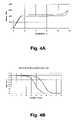
- FIG. 4Ais a graph showing single crystal SMA stress-strain property
- FIG. 4Bis a graph showing the single crystal SMA shape memory property.
- the present inventionprovides fabrication methods and articles of manufacture comprising a thin film component made of a single crystal SMA material which has the property of enabling a large repeatable strain recovery, and methods of making such devices.
- Single crystal SMA materialhas been described in PCT Publication WO 2005/108635 to TiNi Alloy Company for Single Crystal Shape Memory Alloy Devices and Methods.
- SMA materialshave become popular for use as actuators due to their ability to generate substantial stress during shape recovery of large strains during temperature-induced phase transformation.
- the energy density of such actuatorsis high compared to other alternatives, such as electromagnetic, electrostatic, bimetals, piezoelectric, and linear and volume thermal expansion effects of ordinary materials.
- the operating cycle of an SMA actuatorincludes deformation during or after cooling, and subsequent heating which results in a temperature-induced phase transformation and recovery of the deformation.
- SMA actuationis favored where relatively large force and small displacements are required in a device that is small in size and low in mass.
- Shape memoryis the ability of certain alloys to recover plastic deformation, which is based on a diffusionless solid-solid lattice distortive structural phase transformation.
- Shape memory alloyshave the ability to undergo mechanical twinning, or a martensitic or similar reversible solid-state transformation which involves a dimensional change, occurring usually over a narrow temperature change. Twinning structures typically appear at right angles to each other in thin film which can impact the dimensional change.
- the mechanical twinning processgenerally enables a shape produced in one state to be recorded if the temperature is altered back again despite the shape having changed in the interim.
- the performance of shape memory alloy based actuatorsstrongly depends on the amount of recoverable deformation.
- recoverable deformationitself is a function of the lattice distortions which take place during martensitic phase transformation in the particular SMA.
- the amount of possible recoverable strain after uniaxial loadingdepends on the particular crystallographic orientation of the deformation tensor relative to the crystallographic axes of the high temperature (austenite) phase and the sign of applied load (tension or compression).
- the crystal(s)can be described as textured because the thinness of the film results in an apparent loss of some of the crystal variants. For example, alignment of crystallographic axes.
- An advantage of the material produced according to this methodis that the material advantages of single crystal bulk shape memory alloy (e.g., increased recoverable strain and constant stress) is extended to the thin film by growing the crystal in such a way that it has preferred crystallographic orientation, or texture.
- the recoverable strainis strongly orientation dependent, and for the various crystallographic directions it differs by approximately a factor of two.
- the recoverable deformation of polycrystalline SMA alloysdue to the lattice distortion during diffusionless solid-solid phase transition, is substantially lower than is theoretically possible for a given material. The main reason for this is that for a conglomerate of randomly oriented grains (as is normally the case for polycrystalline materials), the average deformation will always be less than the maximum available value for a given grain.
- the diffusionless nature of phase transitions in SMAresults in strict lattice correspondence between the high temperature (austenite) and low temperature (martensite) lattices.
- the strength of the grain in CuAlNi SMAcan be as high as 800 MPa with the potential limit for recoverable deformation up to 9 percent and even higher for special deformation modes. As will be appreciated by those skilled in the art, the strength of the grain for TiNi can be even higher.
- Additional advantages of a single crystal SMAinclude the ability to thermally induce phase transformation and contribute to the recoverable deformation, as in the case for polycrystals, as well as the ability for the thermally induced phase transformation to contribute to the stress-induced martensite-to-martensite phase transitions.
- TiNi thin filmis fabricated in a different set of processes than bulk material. Sputter deposition leaves the material in an amorphous state. This provides an opportunity for crystallization in a specific direction which can be achieved using the methods described herein (giving a preferred orientation) and as a single crystal.
- FIG. 1schematically illustrates a system for carrying out the method of the invention.
- Apparatus 10comprises a heat source 12 .
- Heat source 12can include, but is not limited to, lasers (which could also include suitable focusing optics), intense light sources capable of delivering light in the infrared or visible wavelengths, and scanning electron beams.
- a SMA film 14 layeris provided over a substrate 16 used in fabricating single crystal formation in a thin film.
- the crystals forming the thin film 14may have an anisotropic behavior that is different in different crystal directions. For example, for a Cu—Al—Ni alloy, more than twice the recordable strain in a first plane (e.g.
- Crystals produced according to the methods of this inventionare capable of forming films 1-2 microns thick. This thickness corresponds to a few crystal grains in diameter and provides a good candidate for oriented crystal growth. Further, films as thin as 70 nm having crystal sizes 1-2 microns in diameter can be produced. These films employ 2-dimensional crystals which are advantageous for growing oriented crystals.
- Apparatus 10is scanned in a beam 11 over the surface of film 14 which is carried on substrate 16 .
- No special processing of the substrateis required to practice the invention.
- MEMS processessuch as the use of a sacrificial layer for subsequent removal of film from the substrate, is allowed.
- the substratemay be any suitable size.
- the beamforms a strip which is wide enough to make a swath or sweep, shown by dashed line 18 .
- Arrow 20shows, for example, the direction that the beam travels across the surface of the amorphous material during the method.
- the beam power as well as the beam energy absorption property of the film surfacemust be sufficient to enable heating of the SMA material to crystallization temperature very rapidly so that only a single crystal direction propagates.
- the energy required for crystallization of a particular alloywould be known to a person skilled in the art from a differential scanning calorimetry (DSC) measurement and could vary.
- the apparatussuch as a laser, scans the surface of the material at a speed that is sufficient to enable growth of a single crystal. Material behind the beam is cooled rapidly so that the crystal formed under the beam is stable, that is, no re-crystallization takes place.
- a laser with opticsis used to produce a line focus.
- the line focused laserforms a light beam that sweeps, in a narrow band or swath, over the surface of the material.
- heat of crystallizationwill contribute to the change in temperature, but not significantly.
- the heat of crystallizationis typically 10-50 Joules per gram.
- the heat required to raise the temperaturedepends on the materials and on the temperature and is typically hundreds of Joules per gram. Heating is rapid so as to minimize the heat transferred to the substrate. Cooling is typically rapid (and can thought of as equivalent to quenching) because the substrate 16 is a large heat sink compared to the thin film 14 .
- Crystal growth speeddepends on the sample thickness, so this rate must be adjusted to produce complete crystallization. Crystals typically grow in a period of seconds in very thin film. Optimization is possible and must be done experimentally. If the crystallization is incomplete, a subsequent heat treatment might be used fill in the places that are not completely crystallized. As will be appreciated by those skilled in the art, smaller volumes of crystals may be heated using an electron beam instead of a laser. Further, film thicknesses can range from, for example, 100 nanometers to 10 microns.
- One embodiment of a method of the inventionincludes forming a crystalline thin film.
- the methodcomprises the steps of growing the film from an amorphous state by causing a narrow band of the film to be heated to the crystallization temperature, and moving the heated band across the expanse of film.
- Another embodimentis the method of crystallizing an amorphous thin film comprising the step of moving a line-focused laser beam over the surface of the film. Yet another embodiment is the method that results in a single crystal thin film by the steps of growing the film from an amorphous state by causing a narrow band of the film to be heated to the crystallization temperature/and moving the heated band across the expanse of film. Still another embodiment is an article of thin film formed by crystallization of an amorphous thin film fabricated by the steps of growing the film from an amorphous state by causing a narrow band of the film to be heated to the crystallization temperature, and moving the heated band across the expanse of film. Another embodiment is an expanse of thin film of titanium-nickel that is comprised of a single crystal.
- FIG. 2illustrates a set of method steps of manufacturing a single crystal thin film.
- the methodincludes depositing a layer of amorphous material on a substrate 110 . Thereafter heat is applied to the amorphous material 120 .
- the heatis applied, for example, by a laser, light source, or other mechanism capable of achieving the desired temperature.
- the heatis applied in a narrow strip or band, for example, in a sweeping motion across the surface of the amorphous material in a direction ( 20 in FIG. 1 ).
- One or more passes of the heat stripcan be applied until the desired result is achieved.
- the one or more passesare typically in the same direction in order to promote selective crystal growth in a single direction.
- the heat sourcecan be turned on, applied to the surface of the substrate by sweeping across the surface of the substrate in a single direction, turned off (or directed away from the surface) and returned to the start position, and then applied to the surface again in the same direction. This process is repeated as often as required to achieve the desired results.
- the heat sourceis moved continuously 130 across the amorphous material to heat sequential strips of material; crystallization of the amorphous material 140 occurs. Thereafter a the crystallized material is cooled 150 .
- the cooling stepoccurs quickly and can be achieve by providing, for example, a heat sink.
- the methodcan be performed such that a preferred crystal orientation is imparted to the thin film expanse.
- the methodcan include the use of a seed crystal to initiate the crystallization process, if desired.
- the amorphous expansecan be crystallized into material that is superelastic at room temperature.
- FIG. 3Aare scanning electron microscope (SEM) images 310 of a shape memory thin film formed by vacuum sputter deposition and heat crystallization.
- the grain sizeis about 1-3 micrometers in size. Twinning is observed, generally consisting of plates of sub-micrometer size needles lying at right angles to each other.
- FIG. 3Bis a transmission electron micrograph (TEM) image 320 of a single grain of sputter-deposited shape memory alloy about 70 nanometers thick. The grain is about 1 micrometer in diameter, which is more than ten times its thickness.
- SEMscanning electron microscope
- TEMtransmission electron micrograph
- the single crystal superelastic metal alloy thin filmcan be used to create a wide variety of devices, as would be appreciated by those skilled in the art.
- the three-dimensional thin film shapes and their possible use for medical applicationsare the following: cone shapes adapted for use to retrieve blood clots, particularly clots causing ischemic stroke; cylindrical shapes adapted for use as stents to support blood vessels from collapse and stenosis, and to permit treatment of intracranial aneurysms; cylindrical shapes adapted for use as a scaffold structure for making artificially grown blood vessels of all sizes; hemispherical shapes adapted for insertion into aneurysms to isolate the aneurysm from blood flow in parent blood vessels; dome-shaped structures having multiple layers of thin film are intended to be used in intraocular devices for lens implantation.
- Cones or cylinderswhich are formed from more than two layers of thin film can be adapted to create channels (or pockets) between the two layers allow the insertion of an outer structure into the thin film structure.
- channelsor pockets
- a set of such pocketsare used as means for attaching wires or other external parts of a catheter to the thin film cone and cylinders.
- a short segment of a cylindrical shaped devicecan be inserted into each end of a pair of blood vessels to be joined, in such a way that they exert an outward pressure on the blood vessel lumen tending to keep it open and to return it to an open shape when crushed.
- a third cylinderhaving a larger diameter, is then placed over the ends. This member will exert an inward pressure.
- the resultis an anastomosis of the two blood vessel ends, in which the blood vessel wall is gently pressed between the two inner cylinders and the outer cylinder.
- the outer cylinderwill be stretched so that when it is placed it gently forces the two ends of the blood vessel against each other to form a seal and to promote healing.
- the stress-strain property of single crystal SMAis 100% superelastic, recovering up to 9% strain ( ⁇ 100> direction) when in the austenitic state.
- the plateau stressdepends on the transition temperature and increases at a rate of 3.5 MPa/° C. a graph showing single crystal SMA stress-strain property.
- the transition temperatureis dependent upon the composition and can be tuned to between ⁇ 270° C.-+150° C.
- plotting force versus elongatation (stress v. strain)produces a straight line.
- the stress-strain curve for a superelastic wirehas a plateau because elongation takes place at nearly constant force.
- FIG. 4Bis a graph showing the single crystal SMA shape memory property.
- the thermally induced transition from martensite to austenitecan be used as an actuator.
- the material while in a low temperature state (martensite)can be deformed up to 8% and then heated to full recovery by heating it above its transition temperature, which largely depends on the composition. This process of deformation and heating can result in powerful actuators capable of delivering recovery forces (stresses) up to 500 mPa.
- this methodcan be used to make thin film SMA consisting of multiple crystals that have the same crystalline orientation that lie parallel to each other. Such an arrangement would have the benefit of enhanced strain recovery, such as that exhibited by the single crystal SMA.
- the methodcould be adapted to include, for example, crystallizing a first layer of amorphous material (as described above), depositing another thin layer of amorphous material and then applying the crystallization process to that layer (and repeating as desired).
- a first crystalmay be formed and then one or more subsequent crystals formed using the techniques described herein.
- microactuatorsminiature valves, electric switches, relays, optical switches, a variety of medical devices, improves stents, stent covers, anastomosis devices, self-expanding stents or stent covers, to name a few.
- microactuatorsminiature valves, electric switches, relays, optical switches, a variety of medical devices, improves stents, stent covers, anastomosis devices, self-expanding stents or stent covers, to name a few.
- U.S. Pat. No. 5,325,880 to Johnson et al. for Shape-Memory Alloy Film Actuated MicrovalveU.S. Pat. No. 5,903,099 to Johnson et al. for Fabrication System, Method and Apparatus for Microelectromechanical Devices
Landscapes
- Chemical & Material Sciences (AREA)
- Health & Medical Sciences (AREA)
- Engineering & Computer Science (AREA)
- Materials Engineering (AREA)
- Metallurgy (AREA)
- Organic Chemistry (AREA)
- Mechanical Engineering (AREA)
- Animal Behavior & Ethology (AREA)
- Veterinary Medicine (AREA)
- Epidemiology (AREA)
- Life Sciences & Earth Sciences (AREA)
- General Health & Medical Sciences (AREA)
- Public Health (AREA)
- Chemical Kinetics & Catalysis (AREA)
- Inorganic Chemistry (AREA)
- Heart & Thoracic Surgery (AREA)
- Surgery (AREA)
- Vascular Medicine (AREA)
- Dermatology (AREA)
- Medicinal Chemistry (AREA)
- Oral & Maxillofacial Surgery (AREA)
- Transplantation (AREA)
- Physics & Mathematics (AREA)
- Thermal Sciences (AREA)
- Crystallography & Structural Chemistry (AREA)
- Crystals, And After-Treatments Of Crystals (AREA)
Abstract
Description
- 1. Greater than 9% strain recovery. There is a three fold gain in performance over the conventional SMA materials made from bulk materials. Depending on how the sample is used, the greater than 9%, for example, can either be used in the high temperature state (when in austenite phase) as a hyperelastic spring, or deformed 9% (when in martensite phase) and then heated to recovery as an actuator. Thus, <100> is the preferred direction for an alloy of Cu—Al—Ni according to the crystallographic index and <111> is the preferred direction for an alloy of TiNi according to the crystallographic index. The mechanical properties are not isotropic in materials that undergo a stress-induced martensite transformation. As a result, a wire of single crystal Cu—Al—Ni can be elongated more than 9% and will recover its shape when the deforming force is removed. In contrast, perpendicular to the long axis of the wire it cannot be deformed more than about 4% without breaking.
- 2. True Constant Force Deflection. Unlike polycrystalline materials which reach their strain/stress plateau strength in a gradual fashion and maintain an upward slope when deformed further, single crystal SMA materials have a very sharp and clear plateau strain/stress that provides a truly flat spring rate when deformed up to 9%. As a result, these single crystal SMAs can be described as exhibiting hyperelastic properties because the range of strain recovery is far beyond the maximum strain recovery of both conventional polycrystalline SMA materials and non-SMA metals and allows. An additional benefit is that the strain recovery for materials exhibiting hyperelastic properties is repeatable. Thus, for example, single crystal SMAs exhibiting hyperelasticity benefit from a second stress plateau that can increase the total recoverable strain to 22%.
- 3. Very Narrow Loading-Unloading Hysterisis. As a result there is substantially the same constant force spring rate during both loading (increasing stress) and unloading (decreasing stress).
- 4. Recovery Which is Repeatable and Complete. A drawback of polycrystalline SMA materials is the settling that occurs as the material is cycled back and forth. The settling problem requires the polycrystalline SMA to be either trained as part of the manufacturing process or designed into the application for use such that the permanent deformation which occurs over the first several cycles does not adversely effect the function of the device. In contrast, single crystal SMA do not develop permanent deformaties.
- 5. Very Low Yield Strength when Martensitic. The ability to provide a low yield strength when in the martensitic phase is a property that is useful for designing devices that have two states, e.g. actuators which are two-way.
- 6. Ultra-Low Transition Temperature. Single crystal SMA made from Cu—Al—Ni can be manufactured with transition temperatures close to absolute zero (−270 Celsius). This compares to SMA materials made from TiNi which have a practical transition temperature limit of −100 Celsius. An advantage is the single crystal SMA use in various cryogenic applications as well as the ability to be used as a valve to control flow of cooling medium.
- 7. Intrinsic Hyperelastic Property. TiNi SMA can be conditioned, through a combination of alloying, heat treatment and cold working, to have superelastic properties. Single crystal Cu—Al—Ni SMA has intrinsic hyperelastic properties. Thus, a single crystal of Cu—Al—Ni is hyperelastic immediately after being formed (pulled and quenched) with no further processing required.
- 8. Increased Thermal Cycle Rate. An increased thermal cycle rate, up to at least a kilohertz can be observed. This provides improves strength and fatigue properties compared to bulk materials. Additionally the smaller crystal size typically has no inclusions which means that micro electro-mechanical systems (MEMS) fabrication techniques can be applied to mass production.
Claims (13)
Priority Applications (1)
| Application Number | Priority Date | Filing Date | Title |
|---|---|---|---|
| US11/420,157US7540899B1 (en) | 2005-05-25 | 2006-05-24 | Shape memory alloy thin film, method of fabrication, and articles of manufacture |
Applications Claiming Priority (2)
| Application Number | Priority Date | Filing Date | Title |
|---|---|---|---|
| US68389105P | 2005-05-25 | 2005-05-25 | |
| US11/420,157US7540899B1 (en) | 2005-05-25 | 2006-05-24 | Shape memory alloy thin film, method of fabrication, and articles of manufacture |
Publications (1)
| Publication Number | Publication Date |
|---|---|
| US7540899B1true US7540899B1 (en) | 2009-06-02 |
Family
ID=40672388
Family Applications (1)
| Application Number | Title | Priority Date | Filing Date |
|---|---|---|---|
| US11/420,157Active2027-06-23US7540899B1 (en) | 2005-05-25 | 2006-05-24 | Shape memory alloy thin film, method of fabrication, and articles of manufacture |
Country Status (1)
| Country | Link |
|---|---|
| US (1) | US7540899B1 (en) |
Cited By (14)
| Publication number | Priority date | Publication date | Assignee | Title |
|---|---|---|---|---|
| US8382917B2 (en) | 2007-12-03 | 2013-02-26 | Ormco Corporation | Hyperelastic shape setting devices and fabrication methods |
| WO2013138760A1 (en)* | 2012-03-15 | 2013-09-19 | Dentsply International, Inc. | Medical instrument made of mono-crystalline shape memory alloys and manufacturing methods |
| US8584767B2 (en) | 2007-01-25 | 2013-11-19 | Tini Alloy Company | Sprinkler valve with active actuation |
| US8685183B1 (en) | 2006-12-01 | 2014-04-01 | Ormco Corporation | Method of alloying reactive components |
| US9539372B2 (en) | 2007-11-30 | 2017-01-10 | Ormco Corporation | Biocompatible copper-based single-crystal shape memory alloys |
| US20180142377A1 (en)* | 2016-11-21 | 2018-05-24 | Dentsply International Inc. | Medical Instrument Made of Monocrystalline Shape Memory Alloys and Manufacturing Methods |
| US10106884B2 (en)* | 1999-11-19 | 2018-10-23 | Vactronix Scientific, Llc | Compliant implantable medical devices and methods of making same |
| US10124197B2 (en) | 2012-08-31 | 2018-11-13 | TiNi Allot Company | Fire sprinkler valve actuator |
| US10610620B2 (en) | 2007-07-30 | 2020-04-07 | Monarch Biosciences, Inc. | Method and devices for preventing restenosis in cardiovascular stents |
| CN112935275A (en)* | 2021-01-21 | 2021-06-11 | 哈尔滨工业大学 | Electron beam fuse additive manufacturing method of gradient TiNi shape memory alloy |
| US11040230B2 (en) | 2012-08-31 | 2021-06-22 | Tini Alloy Company | Fire sprinkler valve actuator |
| US20210254237A1 (en)* | 2020-02-19 | 2021-08-19 | Jagannathan Rajagopalan | Synthesis of single crystal films on amorphous substrates |
| US11473157B2 (en)* | 2019-03-05 | 2022-10-18 | Toyota Jidosha Kabushiki Kaisha | Method for manufacturing alloy ribbon piece |
| US11473158B2 (en)* | 2019-03-05 | 2022-10-18 | Toyota Jidosha Kabushiki Kaisha | Method for manufacturing alloy ribbon piece |
Citations (181)
| Publication number | Priority date | Publication date | Assignee | Title |
|---|---|---|---|---|
| US1560335A (en) | 1924-03-27 | 1925-11-03 | American Lurgi Corp | Process of improving alloys and metals |
| US1926925A (en) | 1931-04-07 | 1933-09-12 | Gulf Res & Dev Corp | Pin, bolt, and other connecting device |
| US2060593A (en) | 1934-04-25 | 1936-11-10 | Bauer & Schaurte Rheinische Sc | Metal element and method of making the same |
| US2371614A (en) | 1942-12-31 | 1945-03-20 | Packard Motor Car Co | Engine connecting rod and method of securing parts together |
| US2586556A (en) | 1946-11-23 | 1952-02-19 | Mullikin Alfred | Flexible binder post |
| US2608996A (en) | 1951-08-30 | 1952-09-02 | Forman Ralph | Glass valve |
| US2610300A (en) | 1951-08-07 | 1952-09-09 | Wilson W Walton | Flow control |
| US2647017A (en) | 1951-04-19 | 1953-07-28 | Ind Res Inst | Nozzle |
| US2911504A (en) | 1958-05-15 | 1959-11-03 | Sigmund Cohn Corp | Fuse member and method of making the same |
| US3229956A (en) | 1962-03-02 | 1966-01-18 | Stevens Mfg Co Inc | Diaphragm fluid valve |
| US3351463A (en) | 1965-08-20 | 1967-11-07 | Alexander G Rozner | High strength nickel-base alloys |
| US3357432A (en) | 1965-02-09 | 1967-12-12 | Edwards Lab Inc | Anastomotic coupling |
| US3400906A (en) | 1964-12-23 | 1968-09-10 | Stocklin Emilio | Remote control valve for heating installations |
| US3408890A (en) | 1967-01-27 | 1968-11-05 | Hi Shear Corp | Separable fastener assembly |
| US3445086A (en) | 1966-11-25 | 1969-05-20 | Zyrotron Ind Inc | Snap acting valve and control mechanism therefor |
| US3454286A (en) | 1967-03-01 | 1969-07-08 | Us Navy | Thermally operated release mechanism |
| US3546996A (en) | 1969-04-10 | 1970-12-15 | Atomic Energy Commission | Release latch actuated by temperature excursion |
| US3613732A (en) | 1969-07-17 | 1971-10-19 | Robertshaw Controls Co | Temperature-responsive valve operators |
| US3620212A (en) | 1970-06-15 | 1971-11-16 | Robert D Fannon Jr | Intrauterine contraceptive device |
| US3659625A (en) | 1970-02-16 | 1972-05-02 | Westinghouse Air Brake Co | Drain valve device |
| US3725835A (en) | 1970-07-20 | 1973-04-03 | J Hopkins | Memory material actuator devices |
| US3849756A (en) | 1973-06-14 | 1974-11-19 | American Thermostat Corp | Nitinol activated switch usable as a slow acting relay |
| US3918443A (en) | 1971-10-20 | 1975-11-11 | Ethyl Corp | Method for birth control |
| US3974844A (en) | 1973-06-11 | 1976-08-17 | Texas Instruments Incorporated | Valve |
| US4055955A (en) | 1976-08-16 | 1977-11-01 | Alfred Davis Johnson | Memory alloy heat engine and method of operation |
| US4063831A (en) | 1974-05-28 | 1977-12-20 | Constructions Navales Et Industrielles De La Mediterranee | Bolted joint |
| US4072159A (en) | 1975-02-22 | 1978-02-07 | Toyoki Kurosawa | Emergency valve incorporating thermal foamable plastic material |
| US4096993A (en) | 1977-01-21 | 1978-06-27 | Emerson Electric Co. | Compensated control valve |
| US4177327A (en) | 1978-11-20 | 1979-12-04 | P. R. Mallory & Co. Inc. | Metal-air battery having electrically operated air access vent cover |
| US4176719A (en) | 1976-03-12 | 1979-12-04 | Mather & Platt Limited | Heat sensitive release devices |
| US4195773A (en) | 1977-03-21 | 1980-04-01 | Ralph Ogden | Programmable controller system for industrial process apparatus |
| US4243963A (en) | 1979-04-02 | 1981-01-06 | Gte Automatic Electric Laboratories Incorporated | Construction of a printed wiring card mountable reed relay |
| US4265684A (en)* | 1978-07-26 | 1981-05-05 | Vacuumschmelze Gmbh | Magnetic core comprised of low-retentivity amorphous alloy |
| US4279790A (en) | 1979-07-05 | 1981-07-21 | Kabushiki Kaisha Mikuni Seisakusho | Composite material compositions using wasterpaper and method of producing same |
| US4340049A (en) | 1979-10-18 | 1982-07-20 | Baxter Travenol Laboratories, Inc. | Breakaway valve |
| JPS57161031A (en)* | 1981-03-28 | 1982-10-04 | Nippon Steel Corp | Improving method for watt loss of thin strip of amorphous magnetic alloy |
| EP0053596B1 (en) | 1980-11-28 | 1984-10-17 | Gunnar Liljedahl | Expanding means |
| JPS59179771U (en) | 1983-05-20 | 1984-12-01 | 株式会社小松製作所 | Steering lever device for tracked vehicles |
| US4485545A (en) | 1983-07-07 | 1984-12-04 | Ford Motor Company | Method of attaching a metal shaft to a ceramic shaft and product thereby |
| US4501058A (en) | 1979-08-27 | 1985-02-26 | Pda Engineering | Method of pre-stressing a structural member |
| US4524343A (en) | 1984-01-13 | 1985-06-18 | Raychem Corporation | Self-regulated actuator |
| US4549717A (en) | 1983-03-07 | 1985-10-29 | Leuven Research & Development | Heat responsive valve |
| US4551974A (en) | 1984-04-27 | 1985-11-12 | Raychem Corporation | Shape memory effect actuator and methods of assembling and operating therefor |
| US4553393A (en) | 1983-08-26 | 1985-11-19 | The United States Of America As Represented By The Administrator Of The National Aeronautics And Space Administration | Memory metal actuator |
| US4558715A (en) | 1984-05-16 | 1985-12-17 | Kowatachi International, Ltd. | Apparatus for injecting measured quantities of liquid into a fluid stream |
| US4567549A (en) | 1985-02-21 | 1986-01-28 | Blazer International Corp. | Automatic takeup and overload protection device for shape memory metal actuator |
| US4585209A (en) | 1983-10-27 | 1986-04-29 | Harry E. Aine | Miniature valve and method of making same |
| US4589179A (en) | 1984-09-10 | 1986-05-20 | Caterpillar Tractor Co. | Flexible positioner |
| US4596483A (en) | 1983-07-11 | 1986-06-24 | Leuven Research And Development | Temperature responsive linkage element |
| US4619284A (en) | 1984-03-21 | 1986-10-28 | Societe Nationale Industrielle Aerospatiale | Pyrotechnic valve |
| US4654191A (en) | 1984-06-09 | 1987-03-31 | Kernforschungszentrum Karlsruhe Gmbh | Pressure release arrangement for the safety containment of a pressurized water nuclear reactor |
| US4684913A (en) | 1986-09-05 | 1987-08-04 | Raychem Corporation | Slider lifter |
| GB2187951A (en) | 1986-03-04 | 1987-09-23 | Total Feuerschutz Gmbh | Sprinkler |
| US4706758A (en) | 1984-04-30 | 1987-11-17 | U.S. Fire Control Corporation | Automatic on-off sprinkler head |
| US4753465A (en) | 1986-04-11 | 1988-06-28 | James F. Dalby | Remotely operable locking mechanism |
| SU1434314A1 (en) | 1987-04-02 | 1988-10-30 | Институт Металлургии Им.А.А.Байкова | Joining device |
| US4821997A (en) | 1986-09-24 | 1989-04-18 | The Board Of Trustees Of The Leland Stanford Junior University | Integrated, microminiature electric-to-fluidic valve and pressure/flow regulator |
| US4823607A (en) | 1987-05-18 | 1989-04-25 | Massachusetts Institute Of Technology | Released film structures and method of measuring film properties |
| US4824073A (en) | 1986-09-24 | 1989-04-25 | Stanford University | Integrated, microminiature electric to fluidic valve |
| US4848388A (en) | 1987-10-19 | 1989-07-18 | Memory Metals, Inc. | Emergency valve with test capability |
| US4854797A (en) | 1988-10-05 | 1989-08-08 | Ford Motor Company | Threaded fastener with resilient linking means |
| US4864824A (en) | 1988-10-31 | 1989-09-12 | American Telephone And Telegraph Company, At&T Bell Laboratories | Thin film shape memory alloy and method for producing |
| US4893655A (en) | 1989-08-23 | 1990-01-16 | The United States Of America As Represented By The Secretary Of The Navy | Double valve mechanism for an acoustic modulator |
| US4896728A (en) | 1987-10-02 | 1990-01-30 | Thomas Bolton & Johnson Limited | Fire sprinklers with frangible body closing a flow passage and separate means for shattering same |
| US4943032A (en) | 1986-09-24 | 1990-07-24 | Stanford University | Integrated, microminiature electric to fluidic valve and pressure/flow regulator |
| US5061137A (en) | 1991-04-29 | 1991-10-29 | Ford Motor Company | Fastener with resilient linking means |
| US5060888A (en) | 1989-06-09 | 1991-10-29 | Societe Nationale Industrielle Et Aerospatiale | Temporary linking device, especially for an artificial satellite lengthening piece, and method to free such a link |
| US5061914A (en) | 1989-06-27 | 1991-10-29 | Tini Alloy Company | Shape-memory alloy micro-actuator |
| US5069419A (en) | 1989-06-23 | 1991-12-03 | Ic Sensors Inc. | Semiconductor microactuator |
| US5072288A (en) | 1989-02-21 | 1991-12-10 | Cornell Research Foundation, Inc. | Microdynamic release structure |
| US5114504A (en) | 1990-11-05 | 1992-05-19 | Johnson Service Company | High transformation temperature shape memory alloy |
| US5116252A (en) | 1991-08-02 | 1992-05-26 | Hartman Thomas A | In-line sleeve valve having velocity guide pressure equalization and drive assembly with improved drive pin mountings |
| US5117916A (en) | 1990-04-11 | 1992-06-02 | Hochiki Kabushiki Kaisha | Sprinkler head and operation monitor therefor |
| US5119555A (en) | 1988-09-19 | 1992-06-09 | Tini Alloy Company | Non-explosive separation device |
| US5129753A (en) | 1990-11-13 | 1992-07-14 | Trw Inc. | Shape memory wire latch mechanism |
| US5160233A (en) | 1992-05-13 | 1992-11-03 | The United State Of America As Representd By The Administrator Of The National Aeronautics And Space Administration | Fastening apparatus having shape memory alloy actuator |
| US5190546A (en) | 1983-10-14 | 1993-03-02 | Raychem Corporation | Medical devices incorporating SIM alloy elements |
| US5192147A (en) | 1991-09-03 | 1993-03-09 | Lockheed Missiles & Space Company, Inc. | Non-pyrotechnic release system |
| US5211371A (en) | 1991-07-22 | 1993-05-18 | Advanced Control Technologies, Inc. | Linearly actuated valve |
| US5218998A (en) | 1992-04-01 | 1993-06-15 | Bakken Gary M | Linearly adjustable |
| US5245738A (en) | 1988-09-19 | 1993-09-21 | Tini Alloy Company | Method for securing together and non-explosively separating multiple components |
| US5309717A (en) | 1993-03-22 | 1994-05-10 | Minch Richard B | Rapid shape memory effect micro-actuators |
| US5312152A (en) | 1991-10-23 | 1994-05-17 | Martin Marietta Corporation | Shape memory metal actuated separation device |
| US5325880A (en) | 1993-04-19 | 1994-07-05 | Tini Alloy Company | Shape memory alloy film actuated microvalve |
| US5344117A (en) | 1992-10-10 | 1994-09-06 | Robert Bosch Gmbh | Micro-actuator |
| US5364046A (en) | 1992-02-24 | 1994-11-15 | Environmental Research Institute Of Michigan | Automatic compliant capture and docking mechanism for spacecraft |
| JPH0790624B2 (en) | 1991-03-26 | 1995-10-04 | 積水樹脂株式会社 | Laminate |
| US5494113A (en) | 1994-02-01 | 1996-02-27 | Central Sprinkler Corporation | Sprinklers with shape-memory alloy actuators |
| US5502982A (en) | 1994-04-28 | 1996-04-02 | Liquid Carbonic Industries Corporation | Cryogenic tie pin |
| US5543349A (en) | 1994-08-18 | 1996-08-06 | Kulite Semiconductor Products, Inc. | Method for fabricating a beam pressure sensor employing dielectrically isolated resonant beams |
| US5605543A (en) | 1994-03-10 | 1997-02-25 | Schneider (Usa) Inc. | Catheter having shaft of varying stiffness |
| US5619177A (en) | 1995-01-27 | 1997-04-08 | Mjb Company | Shape memory alloy microactuator having an electrostatic force and heating means |
| US5622225A (en) | 1992-04-23 | 1997-04-22 | Sundholm; Goeran | Quick response sprinkler head |
| US5640217A (en) | 1995-02-02 | 1997-06-17 | Fergaflex, Inc. | Eyeglass frame with very high recoverable deformability |
| US5641364A (en) | 1994-10-28 | 1997-06-24 | The Furukawa Electric Co., Ltd. | Method of manufacturing high-temperature shape memory alloys |
| US5676356A (en) | 1996-05-30 | 1997-10-14 | The Boler Company | Flexible bolster |
| US5695504A (en) | 1995-02-24 | 1997-12-09 | Heartport, Inc. | Devices and methods for performing a vascular anastomosis |
| US5714690A (en) | 1991-12-13 | 1998-02-03 | Honeywell Inc. | Piezoresistive silicon pressure sensor manufacture implementing long diaphragms with large aspect ratios |
| US5722989A (en) | 1995-05-22 | 1998-03-03 | The Regents Of The University Of California | Microminiaturized minimally invasive intravascular micro-mechanical systems powered and controlled via fiber-optic cable |
| JPH10173306A (en) | 1996-12-06 | 1998-06-26 | Olympus Optical Co Ltd | Manufacturing method of shape memory alloy thin-film actuator |
| US5772378A (en) | 1993-11-30 | 1998-06-30 | Kvaerner Tamturbine Oy | Pre-tensioning device for fastening elements and method for pre-tensioning a fastening element |
| US5771742A (en) | 1995-09-11 | 1998-06-30 | Tini Alloy Company | Release device for retaining pin |
| US5796152A (en) | 1997-01-24 | 1998-08-18 | Roxburgh Ltd. | Cantilevered microstructure |
| US5819749A (en) | 1995-09-25 | 1998-10-13 | Regents Of The University Of California | Microvalve |
| US5825275A (en) | 1995-10-27 | 1998-10-20 | University Of Maryland | Composite shape memory micro actuator |
| US5837394A (en) | 1992-05-20 | 1998-11-17 | Brooke Schumm, Jr. | Electric appliance and fluid depolarized cell with low parasitic usage microactuated valve |
| US5840199A (en) | 1994-06-01 | 1998-11-24 | Litton Systems, Inc. | Method for purging a multi-layer sacrificial etched silicon substrate |
| US5850837A (en) | 1996-03-21 | 1998-12-22 | Furukawa Electric Co., Ltd. | Device for correcting an ingrown nail |
| US5867302A (en) | 1997-08-07 | 1999-02-02 | Sandia Corporation | Bistable microelectromechanical actuator |
| WO1998053362A9 (en) | 1997-05-23 | 1999-04-01 | Tini Alloy Co | Fabrication system, method and apparatus for microelectromechanical devices |
| US5924492A (en) | 1996-07-02 | 1999-07-20 | Senju Sprinkler Company Limited | Sprinkler head assembly |
| US5930651A (en) | 1994-04-28 | 1999-07-27 | Ngk Insulators, Ltd. | Method of forming a semiconductor device having a plurality of cavity defined gating regions |
| US5960812A (en) | 1997-07-25 | 1999-10-05 | Tini Alloy Company | Fluid flow control valve |
| WO2000004204A1 (en) | 1998-07-17 | 2000-01-27 | Micro Therapeutics, Inc. | Thin film stent |
| US6042553A (en) | 1997-04-15 | 2000-03-28 | Symbiosis Corporation | Linear elastic member |
| US6072617A (en) | 1996-11-26 | 2000-06-06 | Texas Instruments Incorporated | Micro mechanical device with memory metal component |
| US6075239A (en) | 1997-09-10 | 2000-06-13 | Lucent Technologies, Inc. | Article comprising a light-actuated micromechanical photonic switch |
| US6073700A (en) | 1997-07-25 | 2000-06-13 | Hochiki Kabushiki Kaisha | Sprinkler head |
| JP2000185999A (en) | 1998-12-21 | 2000-07-04 | Tokin Corp | Production of alloy single crystal |
| US6084849A (en) | 1996-05-20 | 2000-07-04 | International Business Machines Corporation | Shape memory alloy recording medium, storage devices based thereon, and method for using these storage devices |
| US6101164A (en) | 1994-01-31 | 2000-08-08 | Matsushita Electric Industrial Co., Ltd. | High density recording by a conductive probe contact with phase change recording layer |
| US6124523A (en) | 1995-03-10 | 2000-09-26 | Impra, Inc. | Encapsulated stent |
| US6126371A (en) | 1999-04-05 | 2000-10-03 | Lockheed Martin Corporation | Shape memory metal alloy preload attenuation device |
| US6139143A (en) | 1997-12-11 | 2000-10-31 | Bausch & Lomb Incorporated | Temple for eyewear having an integrally formed serpentine hinge |
| US6195478B1 (en) | 1998-02-04 | 2001-02-27 | Agilent Technologies, Inc. | Planar lightwave circuit-based optical switches using micromirrors in trenches |
| US6203715B1 (en) | 1999-01-19 | 2001-03-20 | Daewoo Electronics Co., Ltd. | Method for the manufacture of a thin film actuated mirror array |
| US6229640B1 (en) | 1999-08-11 | 2001-05-08 | Adc Telecommunications, Inc. | Microelectromechanical optical switch and method of manufacture thereof |
| US6247493B1 (en) | 2000-03-09 | 2001-06-19 | Richard C. Henderson | Miniature pulsatile flow controller |
| US6277133B1 (en) | 2000-03-17 | 2001-08-21 | Nozomu Kanesaka | Connector for small conduits |
| US6284067B1 (en)* | 1999-07-02 | 2001-09-04 | The University Of Tennessee Research Corporation | Method for producing alloyed bands or strips on pistons for internal combustion engines |
| US20010023010A1 (en) | 1997-05-01 | 2001-09-20 | Fuji Xerox Co. Ltd. | Micro-structure and manufacturing method and apparatus |
| US20020018325A1 (en) | 1990-06-08 | 2002-02-14 | Hitachi, Ltd. | Magnetoresistance effect elements, magnetic heads and magnetic storage apparatus |
| US6386507B2 (en) | 1999-09-01 | 2002-05-14 | Jds Uniphase Corporation | Microelectromechanical valves including single crystalline material components |
| US20020062154A1 (en) | 2000-09-22 | 2002-05-23 | Ayers Reed A. | Non-uniform porosity tissue implant |
| US6406605B1 (en) | 1999-06-01 | 2002-06-18 | Ysi Incorporated | Electroosmotic flow controlled microfluidic devices |
| US6407478B1 (en) | 2000-08-21 | 2002-06-18 | Jds Uniphase Corporation | Switches and switching arrays that use microelectromechanical devices having one or more beam members that are responsive to temperature |
| US6410360B1 (en) | 1999-01-26 | 2002-06-25 | Teledyne Industries, Inc. | Laminate-based apparatus and method of fabrication |
| US6447478B1 (en) | 1998-05-15 | 2002-09-10 | Ronald S. Maynard | Thin-film shape memory alloy actuators and processing methods |
| EP1238600A1 (en) | 2001-03-08 | 2002-09-11 | Thierry Holemans | NA device using shape memory alloys and a bias element to reduce the thermal hysteresis of the phase change |
| US6451668B1 (en) | 1998-12-15 | 2002-09-17 | Fraunhofer Gesellschaft zur Förderung der angewandten Forschung e.V. | Method of producing calibration structures in semiconductor substrates |
| US6454913B1 (en) | 2001-07-12 | 2002-09-24 | Delphi Technologies, Inc. | Process for deposition of sputtered shape memory alloy films |
| US6470108B1 (en) | 2000-04-26 | 2002-10-22 | Tini Alloy Company | Optical switching device and method |
| US6475261B1 (en) | 1997-03-19 | 2002-11-05 | Minoru Matsumoto | NiMnGa alloy with a controlled finish point of the reverse transformation and shape memory effect |
| US20030002994A1 (en) | 2001-03-07 | 2003-01-02 | Johnson A. David | Thin film shape memory alloy actuated flow controller |
| US6524322B1 (en) | 1998-10-23 | 2003-02-25 | Eric Berreklouw | Anastomosis device |
| US6533905B2 (en) | 2000-01-24 | 2003-03-18 | Tini Alloy Company | Method for sputtering tini shape-memory alloys |
| US6537310B1 (en) | 1999-11-19 | 2003-03-25 | Advanced Bio Prosthetic Surfaces, Ltd. | Endoluminal implantable devices and method of making same |
| US20030078465A1 (en) | 2001-10-16 | 2003-04-24 | Suresh Pai | Systems for heart treatment |
| US6582985B2 (en) | 2000-12-27 | 2003-06-24 | Honeywell International Inc. | SOI/glass process for forming thin silicon micromachined structures |
| US6592724B1 (en) | 1999-09-22 | 2003-07-15 | Delphi Technologies, Inc. | Method for producing NiTiHf alloy films by sputtering |
| US6605111B2 (en) | 1998-06-04 | 2003-08-12 | New York University | Endovascular thin film devices and methods for treating and preventing stroke |
| US6614570B2 (en) | 2000-09-29 | 2003-09-02 | Tini Alloy Company | Shutter for fiber optic systems |
| US20030170130A1 (en) | 2002-03-07 | 2003-09-11 | Johnson A. David | Micro-dosing pumps and valves |
| US6620634B2 (en) | 2002-01-17 | 2003-09-16 | Tini Alloy Company | Method of accurately measuring compositions of thin film shape memory alloys |
| US6624730B2 (en) | 2000-03-28 | 2003-09-23 | Tini Alloy Company | Thin film shape memory alloy actuated microrelay |
| US6669794B1 (en)* | 1998-12-04 | 2003-12-30 | Eta Sa Fabriques D'ebauches | Method for treating an object with a laser |
| US6669795B2 (en) | 2002-01-17 | 2003-12-30 | Tini Alloy Company | Methods of fabricating high transition temperature SMA, and SMA materials made by the methods |
| US6672502B1 (en) | 2000-11-28 | 2004-01-06 | The State Of Oregon Acting By And Through The State Board Of Higher Education On Behalf Of Oregon State University | Method for making devices having intermetallic structures and intermetallic devices made thereby |
| US6688828B1 (en) | 2000-12-01 | 2004-02-10 | Arizona Board Of Regents | Self-torquing fasteners |
| US6729599B2 (en) | 2001-06-26 | 2004-05-04 | Tini Alloy Company | Liquid microvalve |
| US6742761B2 (en) | 2001-04-10 | 2004-06-01 | Tini Alloy Company | Miniature latching valve |
| US6746890B2 (en) | 2002-07-17 | 2004-06-08 | Tini Alloy Company | Three dimensional thin film devices and methods of fabrication |
| US6771445B1 (en) | 2000-03-31 | 2004-08-03 | Hitachi Global Storage Technologies Netherlands B.V. | Assembly and method suitable for thermo-magnetic writing/reading of data |
| WO2003052150A3 (en) | 2001-12-19 | 2004-08-12 | Karlsruhe Forschzent | Superelastic element made of a copper alloy and method for imparting and preserving a curvature of a given geometry |
| US6790298B2 (en) | 2000-07-10 | 2004-09-14 | Tini Alloy Company | Method of fabrication of free standing shape memory alloy thin film |
| US6811910B2 (en) | 2001-07-18 | 2004-11-02 | Evionyx, Inc. | Metal air cell incorporating air flow system |
| US20040243219A1 (en) | 2002-02-26 | 2004-12-02 | Harald Fischer | Venous prosthesis |
| US20040249399A1 (en) | 2001-07-17 | 2004-12-09 | Phillippe Cinquin | Device for assembling blood vessels |
| US6840329B2 (en) | 2002-03-06 | 2005-01-11 | Senju Sprinkler Company Limited | Cover assembly for a concealed sprinkler head |
| US6843465B1 (en) | 2003-08-14 | 2005-01-18 | Loren W. Scott | Memory wire actuated control valve |
| US20050113933A1 (en) | 2003-11-24 | 2005-05-26 | Checkmed Systems, Inc. | Stent |
| US6908275B2 (en) | 2002-04-29 | 2005-06-21 | Charles Nelson | Fastener having supplemental support and retention capabilities |
| US6920966B2 (en) | 2003-03-24 | 2005-07-26 | Honeywell International Inc. | Remotely releasable support strut |
| US6955187B1 (en) | 2003-07-16 | 2005-10-18 | Tini Alloy Company | Zinc-air battery control valve |
| EP1122526B1 (en) | 2000-01-31 | 2006-05-03 | Nec Corporation | Thermal infrared detector provided with shield for high fill factor |
| US7040323B1 (en) | 2002-08-08 | 2006-05-09 | Tini Alloy Company | Thin film intrauterine device |
| US7044596B2 (en) | 2004-02-02 | 2006-05-16 | Park Andrew Q | Hingeless eyeglasses frame |
| US20060118210A1 (en) | 2004-10-04 | 2006-06-08 | Johnson A D | Portable energy storage devices and methods |
| WO2005108635A3 (en) | 2004-05-06 | 2007-01-18 | Tini Alloy Co | Single crystal shape memory alloy devices and methods |
| US7201367B2 (en) | 2002-12-12 | 2007-04-10 | Caterpillar Inc | Load-bearing resilient mount |
| US20070246233A1 (en) | 2006-04-04 | 2007-10-25 | Johnson A D | Thermal actuator for fire protection sprinkler head |
- 2006
- 2006-05-24USUS11/420,157patent/US7540899B1/enactiveActive
Patent Citations (187)
| Publication number | Priority date | Publication date | Assignee | Title |
|---|---|---|---|---|
| US1560335A (en) | 1924-03-27 | 1925-11-03 | American Lurgi Corp | Process of improving alloys and metals |
| US1926925A (en) | 1931-04-07 | 1933-09-12 | Gulf Res & Dev Corp | Pin, bolt, and other connecting device |
| US2060593A (en) | 1934-04-25 | 1936-11-10 | Bauer & Schaurte Rheinische Sc | Metal element and method of making the same |
| US2371614A (en) | 1942-12-31 | 1945-03-20 | Packard Motor Car Co | Engine connecting rod and method of securing parts together |
| US2586556A (en) | 1946-11-23 | 1952-02-19 | Mullikin Alfred | Flexible binder post |
| US2647017A (en) | 1951-04-19 | 1953-07-28 | Ind Res Inst | Nozzle |
| US2610300A (en) | 1951-08-07 | 1952-09-09 | Wilson W Walton | Flow control |
| US2608996A (en) | 1951-08-30 | 1952-09-02 | Forman Ralph | Glass valve |
| US2911504A (en) | 1958-05-15 | 1959-11-03 | Sigmund Cohn Corp | Fuse member and method of making the same |
| US3229956A (en) | 1962-03-02 | 1966-01-18 | Stevens Mfg Co Inc | Diaphragm fluid valve |
| US3400906A (en) | 1964-12-23 | 1968-09-10 | Stocklin Emilio | Remote control valve for heating installations |
| US3357432A (en) | 1965-02-09 | 1967-12-12 | Edwards Lab Inc | Anastomotic coupling |
| US3351463A (en) | 1965-08-20 | 1967-11-07 | Alexander G Rozner | High strength nickel-base alloys |
| US3445086A (en) | 1966-11-25 | 1969-05-20 | Zyrotron Ind Inc | Snap acting valve and control mechanism therefor |
| US3408890A (en) | 1967-01-27 | 1968-11-05 | Hi Shear Corp | Separable fastener assembly |
| US3454286A (en) | 1967-03-01 | 1969-07-08 | Us Navy | Thermally operated release mechanism |
| US3546996A (en) | 1969-04-10 | 1970-12-15 | Atomic Energy Commission | Release latch actuated by temperature excursion |
| US3613732A (en) | 1969-07-17 | 1971-10-19 | Robertshaw Controls Co | Temperature-responsive valve operators |
| US3659625A (en) | 1970-02-16 | 1972-05-02 | Westinghouse Air Brake Co | Drain valve device |
| US3620212A (en) | 1970-06-15 | 1971-11-16 | Robert D Fannon Jr | Intrauterine contraceptive device |
| US3725835A (en) | 1970-07-20 | 1973-04-03 | J Hopkins | Memory material actuator devices |
| US3918443A (en) | 1971-10-20 | 1975-11-11 | Ethyl Corp | Method for birth control |
| US3974844A (en) | 1973-06-11 | 1976-08-17 | Texas Instruments Incorporated | Valve |
| US3849756A (en) | 1973-06-14 | 1974-11-19 | American Thermostat Corp | Nitinol activated switch usable as a slow acting relay |
| US4063831A (en) | 1974-05-28 | 1977-12-20 | Constructions Navales Et Industrielles De La Mediterranee | Bolted joint |
| US4072159A (en) | 1975-02-22 | 1978-02-07 | Toyoki Kurosawa | Emergency valve incorporating thermal foamable plastic material |
| US4176719A (en) | 1976-03-12 | 1979-12-04 | Mather & Platt Limited | Heat sensitive release devices |
| US4055955A (en) | 1976-08-16 | 1977-11-01 | Alfred Davis Johnson | Memory alloy heat engine and method of operation |
| US4096993A (en) | 1977-01-21 | 1978-06-27 | Emerson Electric Co. | Compensated control valve |
| US4195773A (en) | 1977-03-21 | 1980-04-01 | Ralph Ogden | Programmable controller system for industrial process apparatus |
| US4265684A (en)* | 1978-07-26 | 1981-05-05 | Vacuumschmelze Gmbh | Magnetic core comprised of low-retentivity amorphous alloy |
| US4177327A (en) | 1978-11-20 | 1979-12-04 | P. R. Mallory & Co. Inc. | Metal-air battery having electrically operated air access vent cover |
| US4243963A (en) | 1979-04-02 | 1981-01-06 | Gte Automatic Electric Laboratories Incorporated | Construction of a printed wiring card mountable reed relay |
| US4279790A (en) | 1979-07-05 | 1981-07-21 | Kabushiki Kaisha Mikuni Seisakusho | Composite material compositions using wasterpaper and method of producing same |
| US4501058A (en) | 1979-08-27 | 1985-02-26 | Pda Engineering | Method of pre-stressing a structural member |
| US4340049A (en) | 1979-10-18 | 1982-07-20 | Baxter Travenol Laboratories, Inc. | Breakaway valve |
| EP0053596B1 (en) | 1980-11-28 | 1984-10-17 | Gunnar Liljedahl | Expanding means |
| JPS57161031A (en)* | 1981-03-28 | 1982-10-04 | Nippon Steel Corp | Improving method for watt loss of thin strip of amorphous magnetic alloy |
| US4549717A (en) | 1983-03-07 | 1985-10-29 | Leuven Research & Development | Heat responsive valve |
| JPS59179771U (en) | 1983-05-20 | 1984-12-01 | 株式会社小松製作所 | Steering lever device for tracked vehicles |
| US4485545A (en) | 1983-07-07 | 1984-12-04 | Ford Motor Company | Method of attaching a metal shaft to a ceramic shaft and product thereby |
| US4596483A (en) | 1983-07-11 | 1986-06-24 | Leuven Research And Development | Temperature responsive linkage element |
| US4553393A (en) | 1983-08-26 | 1985-11-19 | The United States Of America As Represented By The Administrator Of The National Aeronautics And Space Administration | Memory metal actuator |
| US5190546A (en) | 1983-10-14 | 1993-03-02 | Raychem Corporation | Medical devices incorporating SIM alloy elements |
| US4585209A (en) | 1983-10-27 | 1986-04-29 | Harry E. Aine | Miniature valve and method of making same |
| US4524343A (en) | 1984-01-13 | 1985-06-18 | Raychem Corporation | Self-regulated actuator |
| US4619284A (en) | 1984-03-21 | 1986-10-28 | Societe Nationale Industrielle Aerospatiale | Pyrotechnic valve |
| US4551974A (en) | 1984-04-27 | 1985-11-12 | Raychem Corporation | Shape memory effect actuator and methods of assembling and operating therefor |
| US4706758A (en) | 1984-04-30 | 1987-11-17 | U.S. Fire Control Corporation | Automatic on-off sprinkler head |
| US4558715A (en) | 1984-05-16 | 1985-12-17 | Kowatachi International, Ltd. | Apparatus for injecting measured quantities of liquid into a fluid stream |
| US4654191A (en) | 1984-06-09 | 1987-03-31 | Kernforschungszentrum Karlsruhe Gmbh | Pressure release arrangement for the safety containment of a pressurized water nuclear reactor |
| US4589179A (en) | 1984-09-10 | 1986-05-20 | Caterpillar Tractor Co. | Flexible positioner |
| US4567549A (en) | 1985-02-21 | 1986-01-28 | Blazer International Corp. | Automatic takeup and overload protection device for shape memory metal actuator |
| GB2187951A (en) | 1986-03-04 | 1987-09-23 | Total Feuerschutz Gmbh | Sprinkler |
| US4753465A (en) | 1986-04-11 | 1988-06-28 | James F. Dalby | Remotely operable locking mechanism |
| US4684913A (en) | 1986-09-05 | 1987-08-04 | Raychem Corporation | Slider lifter |
| US4943032A (en) | 1986-09-24 | 1990-07-24 | Stanford University | Integrated, microminiature electric to fluidic valve and pressure/flow regulator |
| US4824073A (en) | 1986-09-24 | 1989-04-25 | Stanford University | Integrated, microminiature electric to fluidic valve |
| US4821997A (en) | 1986-09-24 | 1989-04-18 | The Board Of Trustees Of The Leland Stanford Junior University | Integrated, microminiature electric-to-fluidic valve and pressure/flow regulator |
| SU1434314A1 (en) | 1987-04-02 | 1988-10-30 | Институт Металлургии Им.А.А.Байкова | Joining device |
| US4823607A (en) | 1987-05-18 | 1989-04-25 | Massachusetts Institute Of Technology | Released film structures and method of measuring film properties |
| US4896728A (en) | 1987-10-02 | 1990-01-30 | Thomas Bolton & Johnson Limited | Fire sprinklers with frangible body closing a flow passage and separate means for shattering same |
| EP0310439B1 (en) | 1987-10-02 | 1990-12-27 | THOMAS BOLTON & JOHNSON LTD. | Fire sprinklers |
| US4848388A (en) | 1987-10-19 | 1989-07-18 | Memory Metals, Inc. | Emergency valve with test capability |
| US5245738A (en) | 1988-09-19 | 1993-09-21 | Tini Alloy Company | Method for securing together and non-explosively separating multiple components |
| US5119555A (en) | 1988-09-19 | 1992-06-09 | Tini Alloy Company | Non-explosive separation device |
| US4854797A (en) | 1988-10-05 | 1989-08-08 | Ford Motor Company | Threaded fastener with resilient linking means |
| US4864824A (en) | 1988-10-31 | 1989-09-12 | American Telephone And Telegraph Company, At&T Bell Laboratories | Thin film shape memory alloy and method for producing |
| US5072288A (en) | 1989-02-21 | 1991-12-10 | Cornell Research Foundation, Inc. | Microdynamic release structure |
| US5060888A (en) | 1989-06-09 | 1991-10-29 | Societe Nationale Industrielle Et Aerospatiale | Temporary linking device, especially for an artificial satellite lengthening piece, and method to free such a link |
| US5069419A (en) | 1989-06-23 | 1991-12-03 | Ic Sensors Inc. | Semiconductor microactuator |
| US5061914A (en) | 1989-06-27 | 1991-10-29 | Tini Alloy Company | Shape-memory alloy micro-actuator |
| US4893655A (en) | 1989-08-23 | 1990-01-16 | The United States Of America As Represented By The Secretary Of The Navy | Double valve mechanism for an acoustic modulator |
| US5117916A (en) | 1990-04-11 | 1992-06-02 | Hochiki Kabushiki Kaisha | Sprinkler head and operation monitor therefor |
| US20020018325A1 (en) | 1990-06-08 | 2002-02-14 | Hitachi, Ltd. | Magnetoresistance effect elements, magnetic heads and magnetic storage apparatus |
| US5114504A (en) | 1990-11-05 | 1992-05-19 | Johnson Service Company | High transformation temperature shape memory alloy |
| US5129753A (en) | 1990-11-13 | 1992-07-14 | Trw Inc. | Shape memory wire latch mechanism |
| JPH0790624B2 (en) | 1991-03-26 | 1995-10-04 | 積水樹脂株式会社 | Laminate |
| US5061137A (en) | 1991-04-29 | 1991-10-29 | Ford Motor Company | Fastener with resilient linking means |
| US5211371A (en) | 1991-07-22 | 1993-05-18 | Advanced Control Technologies, Inc. | Linearly actuated valve |
| US5116252A (en) | 1991-08-02 | 1992-05-26 | Hartman Thomas A | In-line sleeve valve having velocity guide pressure equalization and drive assembly with improved drive pin mountings |
| US5192147A (en) | 1991-09-03 | 1993-03-09 | Lockheed Missiles & Space Company, Inc. | Non-pyrotechnic release system |
| US5312152A (en) | 1991-10-23 | 1994-05-17 | Martin Marietta Corporation | Shape memory metal actuated separation device |
| US5714690A (en) | 1991-12-13 | 1998-02-03 | Honeywell Inc. | Piezoresistive silicon pressure sensor manufacture implementing long diaphragms with large aspect ratios |
| US5364046A (en) | 1992-02-24 | 1994-11-15 | Environmental Research Institute Of Michigan | Automatic compliant capture and docking mechanism for spacecraft |
| US5218998A (en) | 1992-04-01 | 1993-06-15 | Bakken Gary M | Linearly adjustable |
| US5622225A (en) | 1992-04-23 | 1997-04-22 | Sundholm; Goeran | Quick response sprinkler head |
| US5160233A (en) | 1992-05-13 | 1992-11-03 | The United State Of America As Representd By The Administrator Of The National Aeronautics And Space Administration | Fastening apparatus having shape memory alloy actuator |
| US5837394A (en) | 1992-05-20 | 1998-11-17 | Brooke Schumm, Jr. | Electric appliance and fluid depolarized cell with low parasitic usage microactuated valve |
| US5344117A (en) | 1992-10-10 | 1994-09-06 | Robert Bosch Gmbh | Micro-actuator |
| US5309717A (en) | 1993-03-22 | 1994-05-10 | Minch Richard B | Rapid shape memory effect micro-actuators |
| US5325880A (en) | 1993-04-19 | 1994-07-05 | Tini Alloy Company | Shape memory alloy film actuated microvalve |
| US5772378A (en) | 1993-11-30 | 1998-06-30 | Kvaerner Tamturbine Oy | Pre-tensioning device for fastening elements and method for pre-tensioning a fastening element |
| US6101164A (en) | 1994-01-31 | 2000-08-08 | Matsushita Electric Industrial Co., Ltd. | High density recording by a conductive probe contact with phase change recording layer |
| US5494113A (en) | 1994-02-01 | 1996-02-27 | Central Sprinkler Corporation | Sprinklers with shape-memory alloy actuators |
| US5605543A (en) | 1994-03-10 | 1997-02-25 | Schneider (Usa) Inc. | Catheter having shaft of varying stiffness |
| US5930651A (en) | 1994-04-28 | 1999-07-27 | Ngk Insulators, Ltd. | Method of forming a semiconductor device having a plurality of cavity defined gating regions |
| US5502982A (en) | 1994-04-28 | 1996-04-02 | Liquid Carbonic Industries Corporation | Cryogenic tie pin |
| US5840199A (en) | 1994-06-01 | 1998-11-24 | Litton Systems, Inc. | Method for purging a multi-layer sacrificial etched silicon substrate |
| US5543349A (en) | 1994-08-18 | 1996-08-06 | Kulite Semiconductor Products, Inc. | Method for fabricating a beam pressure sensor employing dielectrically isolated resonant beams |
| US5641364A (en) | 1994-10-28 | 1997-06-24 | The Furukawa Electric Co., Ltd. | Method of manufacturing high-temperature shape memory alloys |
| US5619177A (en) | 1995-01-27 | 1997-04-08 | Mjb Company | Shape memory alloy microactuator having an electrostatic force and heating means |
| US5640217A (en) | 1995-02-02 | 1997-06-17 | Fergaflex, Inc. | Eyeglass frame with very high recoverable deformability |
| US5695504A (en) | 1995-02-24 | 1997-12-09 | Heartport, Inc. | Devices and methods for performing a vascular anastomosis |
| US6124523A (en) | 1995-03-10 | 2000-09-26 | Impra, Inc. | Encapsulated stent |
| US5722989A (en) | 1995-05-22 | 1998-03-03 | The Regents Of The University Of California | Microminiaturized minimally invasive intravascular micro-mechanical systems powered and controlled via fiber-optic cable |
| US5771742A (en) | 1995-09-11 | 1998-06-30 | Tini Alloy Company | Release device for retaining pin |
| US5819749A (en) | 1995-09-25 | 1998-10-13 | Regents Of The University Of California | Microvalve |
| US5825275A (en) | 1995-10-27 | 1998-10-20 | University Of Maryland | Composite shape memory micro actuator |
| US5850837A (en) | 1996-03-21 | 1998-12-22 | Furukawa Electric Co., Ltd. | Device for correcting an ingrown nail |
| US6084849A (en) | 1996-05-20 | 2000-07-04 | International Business Machines Corporation | Shape memory alloy recording medium, storage devices based thereon, and method for using these storage devices |
| US5676356A (en) | 1996-05-30 | 1997-10-14 | The Boler Company | Flexible bolster |
| US5924492A (en) | 1996-07-02 | 1999-07-20 | Senju Sprinkler Company Limited | Sprinkler head assembly |
| US6072617A (en) | 1996-11-26 | 2000-06-06 | Texas Instruments Incorporated | Micro mechanical device with memory metal component |
| JPH10173306A (en) | 1996-12-06 | 1998-06-26 | Olympus Optical Co Ltd | Manufacturing method of shape memory alloy thin-film actuator |
| US5796152A (en) | 1997-01-24 | 1998-08-18 | Roxburgh Ltd. | Cantilevered microstructure |
| US6475261B1 (en) | 1997-03-19 | 2002-11-05 | Minoru Matsumoto | NiMnGa alloy with a controlled finish point of the reverse transformation and shape memory effect |
| US6042553A (en) | 1997-04-15 | 2000-03-28 | Symbiosis Corporation | Linear elastic member |
| US20010023010A1 (en) | 1997-05-01 | 2001-09-20 | Fuji Xerox Co. Ltd. | Micro-structure and manufacturing method and apparatus |
| WO1998053362A9 (en) | 1997-05-23 | 1999-04-01 | Tini Alloy Co | Fabrication system, method and apparatus for microelectromechanical devices |
| US5903099A (en) | 1997-05-23 | 1999-05-11 | Tini Alloy Company | Fabrication system, method and apparatus for microelectromechanical devices |
| US6073700A (en) | 1997-07-25 | 2000-06-13 | Hochiki Kabushiki Kaisha | Sprinkler head |
| US5960812A (en) | 1997-07-25 | 1999-10-05 | Tini Alloy Company | Fluid flow control valve |
| US5867302A (en) | 1997-08-07 | 1999-02-02 | Sandia Corporation | Bistable microelectromechanical actuator |
| US6075239A (en) | 1997-09-10 | 2000-06-13 | Lucent Technologies, Inc. | Article comprising a light-actuated micromechanical photonic switch |
| US6139143A (en) | 1997-12-11 | 2000-10-31 | Bausch & Lomb Incorporated | Temple for eyewear having an integrally formed serpentine hinge |
| US6195478B1 (en) | 1998-02-04 | 2001-02-27 | Agilent Technologies, Inc. | Planar lightwave circuit-based optical switches using micromirrors in trenches |
| US6447478B1 (en) | 1998-05-15 | 2002-09-10 | Ronald S. Maynard | Thin-film shape memory alloy actuators and processing methods |
| US6605111B2 (en) | 1998-06-04 | 2003-08-12 | New York University | Endovascular thin film devices and methods for treating and preventing stroke |
| WO2000004204A1 (en) | 1998-07-17 | 2000-01-27 | Micro Therapeutics, Inc. | Thin film stent |
| US6524322B1 (en) | 1998-10-23 | 2003-02-25 | Eric Berreklouw | Anastomosis device |
| US6669794B1 (en)* | 1998-12-04 | 2003-12-30 | Eta Sa Fabriques D'ebauches | Method for treating an object with a laser |
| US6451668B1 (en) | 1998-12-15 | 2002-09-17 | Fraunhofer Gesellschaft zur Förderung der angewandten Forschung e.V. | Method of producing calibration structures in semiconductor substrates |
| JP2000185999A (en) | 1998-12-21 | 2000-07-04 | Tokin Corp | Production of alloy single crystal |
| US6203715B1 (en) | 1999-01-19 | 2001-03-20 | Daewoo Electronics Co., Ltd. | Method for the manufacture of a thin film actuated mirror array |
| US6410360B1 (en) | 1999-01-26 | 2002-06-25 | Teledyne Industries, Inc. | Laminate-based apparatus and method of fabrication |
| US6126371A (en) | 1999-04-05 | 2000-10-03 | Lockheed Martin Corporation | Shape memory metal alloy preload attenuation device |
| US6406605B1 (en) | 1999-06-01 | 2002-06-18 | Ysi Incorporated | Electroosmotic flow controlled microfluidic devices |
| US6284067B1 (en)* | 1999-07-02 | 2001-09-04 | The University Of Tennessee Research Corporation | Method for producing alloyed bands or strips on pistons for internal combustion engines |
| US6229640B1 (en) | 1999-08-11 | 2001-05-08 | Adc Telecommunications, Inc. | Microelectromechanical optical switch and method of manufacture thereof |
| US6386507B2 (en) | 1999-09-01 | 2002-05-14 | Jds Uniphase Corporation | Microelectromechanical valves including single crystalline material components |
| US6592724B1 (en) | 1999-09-22 | 2003-07-15 | Delphi Technologies, Inc. | Method for producing NiTiHf alloy films by sputtering |
| US6537310B1 (en) | 1999-11-19 | 2003-03-25 | Advanced Bio Prosthetic Surfaces, Ltd. | Endoluminal implantable devices and method of making same |
| US6533905B2 (en) | 2000-01-24 | 2003-03-18 | Tini Alloy Company | Method for sputtering tini shape-memory alloys |
| EP1122526B1 (en) | 2000-01-31 | 2006-05-03 | Nec Corporation | Thermal infrared detector provided with shield for high fill factor |
| US6247493B1 (en) | 2000-03-09 | 2001-06-19 | Richard C. Henderson | Miniature pulsatile flow controller |
| US6277133B1 (en) | 2000-03-17 | 2001-08-21 | Nozomu Kanesaka | Connector for small conduits |
| US7084726B2 (en) | 2000-03-28 | 2006-08-01 | Tini Alloy Company | Thin film shape memory alloy actuated microrelay |
| US6624730B2 (en) | 2000-03-28 | 2003-09-23 | Tini Alloy Company | Thin film shape memory alloy actuated microrelay |
| US6771445B1 (en) | 2000-03-31 | 2004-08-03 | Hitachi Global Storage Technologies Netherlands B.V. | Assembly and method suitable for thermo-magnetic writing/reading of data |
| US6470108B1 (en) | 2000-04-26 | 2002-10-22 | Tini Alloy Company | Optical switching device and method |
| US6790298B2 (en) | 2000-07-10 | 2004-09-14 | Tini Alloy Company | Method of fabrication of free standing shape memory alloy thin film |
| US6407478B1 (en) | 2000-08-21 | 2002-06-18 | Jds Uniphase Corporation | Switches and switching arrays that use microelectromechanical devices having one or more beam members that are responsive to temperature |
| US20020062154A1 (en) | 2000-09-22 | 2002-05-23 | Ayers Reed A. | Non-uniform porosity tissue implant |
| US6614570B2 (en) | 2000-09-29 | 2003-09-02 | Tini Alloy Company | Shutter for fiber optic systems |
| US6672502B1 (en) | 2000-11-28 | 2004-01-06 | The State Of Oregon Acting By And Through The State Board Of Higher Education On Behalf Of Oregon State University | Method for making devices having intermetallic structures and intermetallic devices made thereby |
| US6688828B1 (en) | 2000-12-01 | 2004-02-10 | Arizona Board Of Regents | Self-torquing fasteners |
| US6582985B2 (en) | 2000-12-27 | 2003-06-24 | Honeywell International Inc. | SOI/glass process for forming thin silicon micromachined structures |
| US20030002994A1 (en) | 2001-03-07 | 2003-01-02 | Johnson A. David | Thin film shape memory alloy actuated flow controller |
| EP1238600A1 (en) | 2001-03-08 | 2002-09-11 | Thierry Holemans | NA device using shape memory alloys and a bias element to reduce the thermal hysteresis of the phase change |
| US6742761B2 (en) | 2001-04-10 | 2004-06-01 | Tini Alloy Company | Miniature latching valve |
| US6729599B2 (en) | 2001-06-26 | 2004-05-04 | Tini Alloy Company | Liquid microvalve |
| US6454913B1 (en) | 2001-07-12 | 2002-09-24 | Delphi Technologies, Inc. | Process for deposition of sputtered shape memory alloy films |
| US20040249399A1 (en) | 2001-07-17 | 2004-12-09 | Phillippe Cinquin | Device for assembling blood vessels |
| US6811910B2 (en) | 2001-07-18 | 2004-11-02 | Evionyx, Inc. | Metal air cell incorporating air flow system |
| US20030078465A1 (en) | 2001-10-16 | 2003-04-24 | Suresh Pai | Systems for heart treatment |
| WO2003052150A3 (en) | 2001-12-19 | 2004-08-12 | Karlsruhe Forschzent | Superelastic element made of a copper alloy and method for imparting and preserving a curvature of a given geometry |
| US20040200551A1 (en) | 2001-12-19 | 2004-10-14 | Klaus-Peter Brhel | Superelastic element made of a copper alloy and method for imparting a curvature of a given geometry |
| US6669795B2 (en) | 2002-01-17 | 2003-12-30 | Tini Alloy Company | Methods of fabricating high transition temperature SMA, and SMA materials made by the methods |
| US6620634B2 (en) | 2002-01-17 | 2003-09-16 | Tini Alloy Company | Method of accurately measuring compositions of thin film shape memory alloys |
| US20040243219A1 (en) | 2002-02-26 | 2004-12-02 | Harald Fischer | Venous prosthesis |
| US6840329B2 (en) | 2002-03-06 | 2005-01-11 | Senju Sprinkler Company Limited | Cover assembly for a concealed sprinkler head |
| US20030170130A1 (en) | 2002-03-07 | 2003-09-11 | Johnson A. David | Micro-dosing pumps and valves |
| US6908275B2 (en) | 2002-04-29 | 2005-06-21 | Charles Nelson | Fastener having supplemental support and retention capabilities |
| US6746890B2 (en) | 2002-07-17 | 2004-06-08 | Tini Alloy Company | Three dimensional thin film devices and methods of fabrication |
| US7040323B1 (en) | 2002-08-08 | 2006-05-09 | Tini Alloy Company | Thin film intrauterine device |
| US20060213522A1 (en) | 2002-08-08 | 2006-09-28 | Leticia Menchaca | Thin film intrauterine device |
| US7201367B2 (en) | 2002-12-12 | 2007-04-10 | Caterpillar Inc | Load-bearing resilient mount |
| US6920966B2 (en) | 2003-03-24 | 2005-07-26 | Honeywell International Inc. | Remotely releasable support strut |
| US6955187B1 (en) | 2003-07-16 | 2005-10-18 | Tini Alloy Company | Zinc-air battery control valve |
| US6843465B1 (en) | 2003-08-14 | 2005-01-18 | Loren W. Scott | Memory wire actuated control valve |
| US20050113933A1 (en) | 2003-11-24 | 2005-05-26 | Checkmed Systems, Inc. | Stent |
| US7044596B2 (en) | 2004-02-02 | 2006-05-16 | Park Andrew Q | Hingeless eyeglasses frame |
| WO2005108635A3 (en) | 2004-05-06 | 2007-01-18 | Tini Alloy Co | Single crystal shape memory alloy devices and methods |
| US20070137740A1 (en) | 2004-05-06 | 2007-06-21 | Atini Alloy Company | Single crystal shape memory alloy devices and methods |
| US20060118210A1 (en) | 2004-10-04 | 2006-06-08 | Johnson A D | Portable energy storage devices and methods |
| US20070246233A1 (en) | 2006-04-04 | 2007-10-25 | Johnson A D | Thermal actuator for fire protection sprinkler head |
Non-Patent Citations (29)
| Title |
|---|
| Antonov et al.; New advances and developments in the Stepnakov method for the growth of shaped crystals; Crystallography Reports; vol. 47; Suppl. 1; 2002; pp. S43-S52. |
| Buchaillot L. et al., "Thin film of titanium/nickel shape memory alloy for multi-degree of freedom microactuators", Seisan Kenkyu, vol. 51, No. 8, 1999, pp. 22-23. |
| ElastametTM brochure from New Discovery Metals; 2007. |
| ElastametTM website screen capture, accessed Jul. 23, 2008. |
| Fu et al.; The growth characteristics with a shape memory effect; J. Phys.: Condens. Matter; vol. 4; 1992; pp. 8303-8310. |
| I. E. Viahhi; Robototechnic Constructions Based On CU-AL-NI Single Crystal Actuators; Proceedings of Second International Conference on Shape Memory and Superelastic Technologies; 1997; United States. |
| Johnson A. D. et al., "Application of shape memory alloys: advantages, disadvantages, and limitations", Micromachining and Microfabrication Process Technology VII, Oct. 22-24, 2001, San Francisco, CA, USA, vol. 4557, 2001, pp. 341-351. |
| Johnson, Alfred David; U.S. Appl. No. 12/182,119 entitled "Method and devices for preventing restenosis in cardiovascular stents," filed Jul. 29, 2008. |
| Johnson, David et al.; U.S. Appl. No. 10/972,745 entitled "Non-explosive releasable coupling device," filed Oct. 25, 2004. |
| Johnson, David et al.; U.S. Appl. No. 11/006,501 entitled "Anastomosis device and method," filed Dec. 6, 2004. |
| Johnson, David et al.; U.S. Appl. No. 11/041,185 entitled "Single crystal Shape memory alloy devices and methods," filed Jan. 24, 2005. |
| Johnson, David et al.; U.S. Appl. No. 11/948,852 entitled "Method of alloying reactive elemental components," filed Nov. 30, 2007. |
| Johnson, David et al.; U.S. Appl. No. 11/949,663 entitled "Hyperelastic shape setting devices and fabrication methods," filed Dec. 3, 2007. |
| Johnson, David et al.; U.S. Appl. No. 12/019,553 entitled "Frangible shape memory alloy fire sprinkler valve actuator," filed Jan. 24, 2008. |
| Johnson, David; U.S. Appl. No. 11/396,234 entitled "Tear-resistant thin film methods of fabrication," filed Mar. 31, 2006. |
| Johnson, David; U.S. Appl. No. 11/415,885 entitled "Eyeglass frame," filed May 2, 2006. |
| Johnson, David; U.S. Appl. No. 11/526,138 entitled "Constant load bolt," filed Sep. 22, 2006. |
| Johnson, David; U.S. Appl. No. 11/859,697 entitled "Constant load fastener," filed Sep. 21, 2007. |
| Martynov, V., "TiNi thin films for microactuators and microdevices: sputter deposition and processing techniques", Thermec' 2003, Internat'l Conf. on Processing and Manufacturing of Advanced Materials, Jul. 7-11, 2003, Leganes, Madrid, Spain, Materials Science Forum, Jul. 7, 2003 vol. 426-432; pp. 3475-3480. |
| Morgan; Medical shape memory alloy applications-the market and its products; Materials Science and engineering A 378; 2004; pp. 16-23. |
| Pauling, Linus, College Chemistry, second edition, W.H. Freeman and Company, San Francisco, 1955, pp. 81-91. |
| Qingfu et al.; Stabilisation of martensite during training of Cu-Al-Ni single crystals; Journal de Physique IV; Collloqu C2; Supplement to the Journa de Physique III; vol. 5; Feb. 1995; pp. 181-186. |
| Recarte et al.; Influence of Al and Ni concentration on the martensitic transformation in Cu-Al-Ni shape-memory alloys; Metallurgical and Materials Transactions A; vol. 33A; Aug. 2002; pp. 2581-2591. |
| Sittner et al.; Stress induced martensitic transformations in tension/torsion of CuAlNi single crystal tube; Scripta Materialia; vol. 48; 2003; pp. 1153-1159. |
| Sutuo et al.; Development of medical guide wire of Cu-Al-Mn-base superelastic alloy with functionally graded characteristics; Mater Res Part B: Appl Biomater; vol. 69B; 2004; pp. 64-69. |
| Takabayashi et al., "Reversible shape memory alloy film fabricated by RF sputtering", Materials and Manufacturing Processes, vol. 13, No. 2, 1998, pp. 275-286. |
| Xiaogdang, MA; U.S. Appl. No. 10/972,759 entitled "Magnetic data storage system," filed Oct. 25, 2004. |
| Zhang et al.; The variant selection criteria in single-crystal CuAlNi shape memory alloys; Smart Mater. Struct.; vol. 9; 2000; pp. 571-581. |
| Zhdanov et al.; Thermal stresses in tubes, produced from a melt by the Stepanov method, during their coiling; Journal of Engineering Physics and Thermophysics; vol. 68; No. 1; 1995; pp. 80-89. |
Cited By (20)
| Publication number | Priority date | Publication date | Assignee | Title |
|---|---|---|---|---|
| US10106884B2 (en)* | 1999-11-19 | 2018-10-23 | Vactronix Scientific, Llc | Compliant implantable medical devices and methods of making same |
| US8685183B1 (en) | 2006-12-01 | 2014-04-01 | Ormco Corporation | Method of alloying reactive components |
| US10190199B2 (en) | 2006-12-01 | 2019-01-29 | Ormco Corporation | Method of alloying reactive components |
| US9340858B2 (en) | 2006-12-01 | 2016-05-17 | Ormco Corporation | Method of alloying reactive components |
| US8584767B2 (en) | 2007-01-25 | 2013-11-19 | Tini Alloy Company | Sprinkler valve with active actuation |
| US10610620B2 (en) | 2007-07-30 | 2020-04-07 | Monarch Biosciences, Inc. | Method and devices for preventing restenosis in cardiovascular stents |
| US9539372B2 (en) | 2007-11-30 | 2017-01-10 | Ormco Corporation | Biocompatible copper-based single-crystal shape memory alloys |
| US9127338B2 (en) | 2007-12-03 | 2015-09-08 | Ormco Corporation | Hyperelastic shape setting devices and fabrication methods |
| US8382917B2 (en) | 2007-12-03 | 2013-02-26 | Ormco Corporation | Hyperelastic shape setting devices and fabrication methods |
| CN104411854B (en)* | 2012-03-15 | 2017-04-26 | 登士柏国际公司 | Medical instrument made of mono-crystalline shape memory alloys and manufacturing methods |
| CN104411854A (en)* | 2012-03-15 | 2015-03-11 | 登士柏国际公司 | Medical instrument made of mono-crystalline shape memory alloys and manufacturing methods |
| WO2013138760A1 (en)* | 2012-03-15 | 2013-09-19 | Dentsply International, Inc. | Medical instrument made of mono-crystalline shape memory alloys and manufacturing methods |
| US10124197B2 (en) | 2012-08-31 | 2018-11-13 | TiNi Allot Company | Fire sprinkler valve actuator |
| US11040230B2 (en) | 2012-08-31 | 2021-06-22 | Tini Alloy Company | Fire sprinkler valve actuator |
| US20180142377A1 (en)* | 2016-11-21 | 2018-05-24 | Dentsply International Inc. | Medical Instrument Made of Monocrystalline Shape Memory Alloys and Manufacturing Methods |
| US11473157B2 (en)* | 2019-03-05 | 2022-10-18 | Toyota Jidosha Kabushiki Kaisha | Method for manufacturing alloy ribbon piece |
| US11473158B2 (en)* | 2019-03-05 | 2022-10-18 | Toyota Jidosha Kabushiki Kaisha | Method for manufacturing alloy ribbon piece |
| US20210254237A1 (en)* | 2020-02-19 | 2021-08-19 | Jagannathan Rajagopalan | Synthesis of single crystal films on amorphous substrates |
| CN112935275A (en)* | 2021-01-21 | 2021-06-11 | 哈尔滨工业大学 | Electron beam fuse additive manufacturing method of gradient TiNi shape memory alloy |
| CN112935275B (en)* | 2021-01-21 | 2022-06-28 | 哈尔滨工业大学 | A kind of electron beam fuse additive manufacturing method of gradient TiNi shape memory alloy |
Similar Documents
| Publication | Publication Date | Title |
|---|---|---|
| US7540899B1 (en) | Shape memory alloy thin film, method of fabrication, and articles of manufacture | |
| Miyazaki | My experience with Ti–Ni-based and Ti-based shape memory alloys | |
| Lee et al. | Two-way 4D printing: a review on the reversibility of 3D-printed shape memory materials | |
| US6669794B1 (en) | Method for treating an object with a laser | |
| Ishida et al. | Sputter-deposited shape-memory alloy thin films: properties and applications | |
| JP2004518510A (en) | Shape memory device whose shape changes with small temperature changes | |
| IL203162A (en) | Methods of processing nickel-titanium shape memory alloys | |
| WO1996039547A2 (en) | Multiple source deposition of shape-memory alloy thin films | |
| Duerig et al. | SMA: smart materials for medical applications | |
| Parvizi et al. | NiTi shape memory alloys: properties | |
| Johnson et al. | Applications of shape memory alloys: advantages, disadvantages, and limitations | |
| CA3150096C (en) | Wires of superelastic nickel-titanium alloy and methods of forming the same | |
| Avery et al. | Reverse Engineering of Nitinol Vena Cava Filters | |
| Jardine et al. | Characterization of the deposition and materials parameters of thin-film TiNi for microactuators and smart materials | |
| Belyaev et al. | Mechanical and functional properties of amorphous–crystalline thin ribbons ofTi50Ni25Cu25 andTi40. 7Hf9. 5Ni44. 8Cu5 shape memory alloys | |
| Mohammed et al. | Preparation and characterization of equiatomic NiTi shape memory alloy | |
| Biffi et al. | Laser-induced superelasticity in NiTinol stent strut | |
| Biffi et al. | Laser shape setting of superelastic NiTi wire: effects of laser beam power and axial pre-load | |
| Lai et al. | The characterization of TiNi shape-memory actuated microvalves | |
| Kumar | Nitinol-based shape-memory alloys | |
| Shelyakov et al. | Microtweezers on the basis of two-way shape memory alloy ribbon | |
| RU2808118C2 (en) | METHOD FOR PRODUCING TiNi ALLOY WITH VARIABLE CHEMICAL COMPOSITION USING ADDITIVE TECHNOLOGIES | |
| Mehrabi | Characterization and Optimization of the Two-Way Effect in Melt-spun NiTi-based Shape Memory Alloys | |
| Curtis | SCALABLE MANUFACTURING OF THIN-FILM SHAPE MEMORY ALLOYS FOR ELECTRONICS, AEROSPACE SYSTEMS, AND ROBOTICS. | |
| Mahmud | Thermomechanical treatment of Ni-Ti shape memory alloy |
Legal Events
| Date | Code | Title | Description |
|---|---|---|---|
| AS | Assignment | Owner name:TINI ALLOY COMPANY, CALIFORNIA Free format text:ASSIGNMENT OF ASSIGNORS INTEREST;ASSIGNOR:JOHNSON, A. DAVID;REEL/FRAME:017853/0548 Effective date:20060607 | |
| STCF | Information on status: patent grant | Free format text:PATENTED CASE | |
| REMI | Maintenance fee reminder mailed | ||
| FPAY | Fee payment | Year of fee payment:4 | |
| SULP | Surcharge for late payment | ||
| AS | Assignment | Owner name:NSVASCULAR, INC., CALIFORNIA Free format text:ASSIGNMENT OF ASSIGNORS INTEREST;ASSIGNOR:TINI ALLOY COMPANY;REEL/FRAME:032322/0818 Effective date:20120511 | |
| FPAY | Fee payment | Year of fee payment:8 | |
| AS | Assignment | Owner name:MONARCH BIOSCIENCES, INC., CALIFORNIA Free format text:CHANGE OF NAME;ASSIGNOR:NSVASCULAR, INC.;REEL/FRAME:047147/0665 Effective date:20180205 | |
| FEPP | Fee payment procedure | Free format text:MAINTENANCE FEE REMINDER MAILED (ORIGINAL EVENT CODE: REM.); ENTITY STATUS OF PATENT OWNER: SMALL ENTITY | |
| FEPP | Fee payment procedure | Free format text:11.5 YR SURCHARGE- LATE PMT W/IN 6 MO, SMALL ENTITY (ORIGINAL EVENT CODE: M2556); ENTITY STATUS OF PATENT OWNER: SMALL ENTITY | |
| MAFP | Maintenance fee payment | Free format text:PAYMENT OF MAINTENANCE FEE, 12TH YR, SMALL ENTITY (ORIGINAL EVENT CODE: M2553); ENTITY STATUS OF PATENT OWNER: SMALL ENTITY Year of fee payment:12 |