US7539803B2 - Bi-directional interface for low data rate application - Google Patents
Bi-directional interface for low data rate applicationDownload PDFInfo
- Publication number
- US7539803B2 US7539803B2US10/461,671US46167103AUS7539803B2US 7539803 B2US7539803 B2US 7539803B2US 46167103 AUS46167103 AUS 46167103AUS 7539803 B2US7539803 B2US 7539803B2
- Authority
- US
- United States
- Prior art keywords
- interface
- signal
- conductor interface
- tia
- voltage
- Prior art date
- Legal status (The legal status is an assumption and is not a legal conclusion. Google has not performed a legal analysis and makes no representation as to the accuracy of the status listed.)
- Expired - Fee Related, expires
Links
- 239000004020conductorSubstances0.000claimsabstractdescription49
- 238000000034methodMethods0.000claimsdescription12
- 230000005540biological transmissionEffects0.000claimsdescription11
- 230000006854communicationEffects0.000claimsdescription8
- 238000004891communicationMethods0.000claimsdescription8
- 230000004044responseEffects0.000claimsdescription6
- 230000008859changeEffects0.000claimsdescription2
- 238000001514detection methodMethods0.000abstractdescription3
- 230000003287optical effectEffects0.000description20
- 238000012546transferMethods0.000description11
- 239000000872bufferSubstances0.000description7
- 230000008569processEffects0.000description6
- 235000004348Perilla frutescensNutrition0.000description5
- 244000124853Perilla frutescensSpecies0.000description5
- 230000005693optoelectronicsEffects0.000description5
- 238000010586diagramMethods0.000description4
- 230000001960triggered effectEffects0.000description4
- 239000000835fiberSubstances0.000description3
- 238000012545processingMethods0.000description3
- 230000000630rising effectEffects0.000description3
- 230000007175bidirectional communicationEffects0.000description2
- 230000003111delayed effectEffects0.000description2
- 238000012986modificationMethods0.000description2
- 230000004048modificationEffects0.000description2
- 238000004806packaging method and processMethods0.000description2
- 238000011084recoveryMethods0.000description2
- 230000008901benefitEffects0.000description1
- 238000006243chemical reactionMethods0.000description1
- 238000011161developmentMethods0.000description1
- 230000000977initiatory effectEffects0.000description1
- 239000002184metalSubstances0.000description1
- 238000012544monitoring processMethods0.000description1
- 230000006855networkingEffects0.000description1
- 230000003071parasitic effectEffects0.000description1
- 230000009467reductionEffects0.000description1
- 230000008054signal transmissionEffects0.000description1
- 230000001360synchronised effectEffects0.000description1
Images


Classifications
- H—ELECTRICITY
- H04—ELECTRIC COMMUNICATION TECHNIQUE
- H04B—TRANSMISSION
- H04B10/00—Transmission systems employing electromagnetic waves other than radio-waves, e.g. infrared, visible or ultraviolet light, or employing corpuscular radiation, e.g. quantum communication
- H04B10/50—Transmitters
- H04B10/501—Structural aspects
- H04B10/503—Laser transmitters
- H—ELECTRICITY
- H04—ELECTRIC COMMUNICATION TECHNIQUE
- H04B—TRANSMISSION
- H04B10/00—Transmission systems employing electromagnetic waves other than radio-waves, e.g. infrared, visible or ultraviolet light, or employing corpuscular radiation, e.g. quantum communication
- H04B10/40—Transceivers
- H—ELECTRICITY
- H04—ELECTRIC COMMUNICATION TECHNIQUE
- H04B—TRANSMISSION
- H04B10/00—Transmission systems employing electromagnetic waves other than radio-waves, e.g. infrared, visible or ultraviolet light, or employing corpuscular radiation, e.g. quantum communication
- H04B10/60—Receivers
- H04B10/66—Non-coherent receivers, e.g. using direct detection
Definitions
- This inventionrelates to optical transmission and particularly to an interface for communication of system information among components of an optical transceiver.
- communications signalsare regularly transported through networks via optical transmission arrangements in order to take advantage of the larger bandwidth available with optical signals transported over fiber optic media.
- optical transportis effected by conversion of an electrical signal to be transmitted into a light signal through the use of a Laser Driver and laser diode which is interfaced to a fiber optic cable.
- the transmitted light signalis converted back to an electrical signal by a photo diode.
- a Laser Driverand associated electronics
- a Photo diodeand its associated electronics
- Opto-electronic transceiver modulesprovide for the bi-directional transmission of data between an electrical interface and an optical data link.
- the modulereceives electrically encoded data signals that are converted into optical signals and transmitted over the optical data link.
- the modulereceives optically encoded data signals that are converted into electrical signals and transmitted onto the electrical interface.
- SFFSmall Form Factor
- the SFF standard for opto-electronic transceiversspecifies minimum transceiver functionality and spells out transceiver physical dimensions.
- the module dimensionsresult in tight size constraints for the transceiver components.
- the receive part of the transceivertypically uses a photodiode (which converts an input light signal to an output current) combined with a transimpedance amplifier (TIA) to convert the photodiode output into a voltage for further processing and data recovery.
- TIAtransimpedance amplifier
- the photodiode and TIAare usually mounted together in a package known as a “TO” can in order to keep the parasitic capacitance and inductance to a minimum for high data-rate transmission systems (e.g., 2.5 Gb/s and higher data rates). That combination of photodiode and TIA mounted in a TO-can will be referred to herein from time to time as the “receive module.”
- the TO-canmust be small to fit inside the SFF transceiver, and this size constraint severely limits the TO-can pin count.
- the photodiode of the receive moduleis usually either a PIN diode or an avalanche photo diode (APD). Most PIN diode applications use 4-pin TO-cans and APD diode applications use 5-pin TO-cans.
- the inventionprovides a bi-directional communications interface that can be implemented using, at most, one additional pin of the receive module TO-can.
- the inventionprovides a bi-directional single-conductor interface comprising (1) a switching means for applying a voltage level to the interface that is outside a normal voltage operating range for the interface and for removing the applied voltage level at an end of a specified time duration; and (2) a timer initiated by detection of the applied voltage and arranged to include a timing interval following removal of the applied voltage.
- a switching meansfor applying a voltage level to the interface that is outside a normal voltage operating range for the interface and for removing the applied voltage level at an end of a specified time duration
- a timerinitiated by detection of the applied voltage and arranged to include a timing interval following removal of the applied voltage.
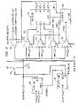
- FIG. 1schematically depicts an SFF optical transceiver.
- FIG. 2shows a schematic view of components of an embodiment of the single-pin interface of the invention.
- FIG. 3is a timing diagram for operation of the embodiment of FIG. 2 .
- FIG. 4shows a schematic view of components of another embodiment of the single-pin interface of the invention.
- FIG. 5is a timing diagram for operation of the embodiment of FIG. 4 .
- FIG. 6shows a schematic view of components of still another embodiment of the single-pin interface of the invention.
- FIG. 7shows a schematic view of components of a still further embodiment of the single-pin interface of the invention.
- a transceiver moduleis interfaced with a host device—such as a switch, hub, router, optical distribution frame and the like—via a compatible connection port.
- a host devicesuch as a switch, hub, router, optical distribution frame and the like
- a compatible connection portsuch as a switch, hub, router, optical distribution frame and the like.
- FIG. 1A functional schematic of an SFF optical transceiver is shown in FIG. 1 .
- the Laser Driver 101 and the included System Interface 103constitute the transmitter portion of the transceiver, while the receiver portion includes the Transimpedance Amplifier (TIA) and Photodiode module 105 operating in combination with the Data Recovery Circuits 107 (for processing the received information—output from the TIA).
- the System Interface 103 associated with the Laser Driver 101operates to handle the communication of system information between the SFF optical transceiver and the outside world. For example, if a system operator wanted to program new system parameters into the TIA of the transceiver, those parameters would initially be sent to the System Interface portion of the Laser Driver. Then the Laser Driver would send those new parameters to the TIA via the interface 109 shown in FIG. 1 .
- the Photodiode and the TIAare packaged together in a TO can package to accommodate a requirement for close proximity between these two elements of the receiver.
- the TIAis constituted as a very small chip, partly to comport with the limited space available in the TO can and partly to address cost constraints.
- the additional signals to be communicated between the Laser Driver and the photodiode-TIA modulewill be transmitted via a bi-directional interface using a single additional pin for the Photodiode-TIA module—i.e., using a 5-pin TO can package for PIN photodiode applications or a 6-pin TO can package for APD photodiode applications. Otherwise, if more than one additional pin is required for the communication of these additional signals (at least in the case of an APD photodiode), it will be necessary to change the module packaging to a relatively non-standard 7 pin TO can package. This would result in not only higher costs for the new packaging, but, potentially, reliability problems as well.
- the inventorsRecognizing that the communication of the additional signals between the Laser Driver and the Photodiode-TIA module can be implemented at a relatively slow data rate, the inventors have developed a new bi-directional interface that can be implemented via a single pin in the Photodiode-TIA module and little increase in circuit complexity for the TIA.
- the single-pin bi-directional interface of the inventionis described hereafter.
- two system-information signalsare to be added to the system information exchanged between the Laser Driver and the Photodiode-TIA module of an SFF optical transceiver.
- the first signalis used to select gain bandwidth circuitry in the TIA to optimize both frequency and signal-to-noise response for each of the data rates from 155 Mb/s to 2.5 Gb/s—to thereby allow one receive module to be used with different rate systems.
- the TIAis required, in the Small Form Factor standard (SFF-8472), to report receive optical signal strength. If a pin were dedicated for each function, the receive module would require moving from a widely available 6-pin TO can package to a 7-pin package when an avalanche photodiode is used. The 7-pin package has fewer suppliers and those suppliers that do offer 7-pin TO-can packages have reported reliability problems due to pin crowding causing signal integrity problems and metal fatigue at the base of the joints.
- the inventorshave developed an interface based on the use of a biasing arrangement to establish the direction of signal transmission on the interface and the use of timers to determine the duration of data transmission.
- the TIAsends signal strength information to the Laser Driver, and the Laser Driver sends rate setting data to the TIA over the same wire.
- the single-pin bi-directional interface of the inventionis hereafter described in the context of four illustrative embodiments of the invention.
- informationis sent from the Laser Driver to the TIA in a single two-bit increment.
- the second and third embodimentssend multiple two-bit words, and in the fourth embodiment, a simplified interface is described for sending multiple one-bit words.
- FIG. 2A schematic depiction of the elements of the single pin interface of the invention for communicating a single two-bit word from the Laser Driver to the TIA is shown in FIG. 2 .
- components of the interface associated with the Laser Driverare shown on the left side of the center dividing line and components of the interface associated with the TIA are shown on the right side of that divide.
- both the Laser Driver and the TIAinclude other components for carrying out their other functions, but only the components associated with the interface of the invention are shown here for ease of illustration.
- the maximum swing of the TIA receive signal power levelis restricted to be less than the power supply voltage (VCC), and the Laser Driver is accordingly able to control the direction of signal flow on the LD_TIA Single-Conductor Interface 201 between the Laser Driver and the TIA by forcing the voltage on that line outside the allowed TIA drive range.
- VCCpower supply voltage
- the Laser Driveris accordingly able to control the direction of signal flow on the LD_TIA Single-Conductor Interface 201 between the Laser Driver and the TIA by forcing the voltage on that line outside the allowed TIA drive range.
- the TIAis put into a listen mode and the Laser Driver then sends the data rate setting to the TIA.
- Timersare established in the TIA and Laser Driver to control the time duration for sending the rate setting information to the TIA and to permit the TIA to latch the setting.
- the interfaceWith the time-out of those timers, the interface then reverts back to the Laser-Driver receive mode, during which the TIA sends the receive signal strength signal to the Laser Driver.
- edge-triggered timersare used in the Laser Driver and TIA to simplify timing constraints.
- the TIA Low Output Drive Buffer 204which buffers the optical receive power level in the TIA, is designed to have relatively small output drive current and to have its maximum positive swing less than VREF3, which is a defined reference voltage level corresponding to the voltage level at which the signal direction of the single conductor interface between the Laser Driver and the TIA is switched.
- This switching pointis sensed by Direction Sense Comparator 206 , which operates to start TIA Timer 208 .
- Comparators 210 , 212 and 214receive rate setting information from the Laser Driver and provide such information as in input to TIA Rate Decode 220 .
- DAC 207receives the rate (rate 0 or rate 1) to be sent to the TIA from the System Interface/Controller 103 (of FIG. 1 ) and outputs it as an analog signal on the single line interface. Operation of DAC 207 is initiated by an enabling signal from Rate Write Timer 205 . That Timer also drives switch 209 to apply supply voltage (VCC) to the single line interface when it is switched to an on state.
- VCCsupply voltage
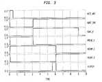
- FIG. 3showing rate-setting timing sequences, in conjunction with FIG. 2 .
- the time axis in FIG. 3is in arbitrary units. The purpose is to show the relative timing sequence, not absolute time values.
- the Laser Driveris operating in the receive mode—i.e., receiving signal-strength signals from the TIA, and that the invention then operates to reverse the direction of signal flow on the single line interface so as to place the TIA into its listen mode.
- the process by which the signal direction on the single-line interface of this embodiment is changedis hereafter described.
- the Laser Driver DAC 207is in a powered down state and its output is in a high impedance state.
- the 210 - 214 Comparators in the TIAare in a powered down state and Low Output Drive Buffer 204 is driving the Laser Driver Monitor A/D (not shown) with the optical receive power level signal.
- Direction Sense Comparator 206is active and monitoring the voltage level on the LD_TIA Single-Conductor Interface 201 .
- the Laser Driverinitiates the TIA rate (bandwidth) setting function (i.e., placing the TIA in its listen mode) by pulsing the Rate_Write signal input to Rate Write Timer 205 (corresponding to the VRTE_WRT timing signal trace in FIG. 3 ).
- the timeris positive edge triggered to make the pulses for the enable signal to DAC 207 , DAC_ENABLE (corresponding to the VDAC_E timing trace in FIG. 3 ), and the driving signal for Switch 209 , WRITE_INITIATE (corresponding to the VWRT_INT timing trace in FIG. 3 ), independent of the Controller pulse width.
- the Rate Write Timer 205In response to the Rate_Write signal at its input, the Rate Write Timer 205 initially drives the Write_Initiate signal to Switch 209 low, causing Switch 209 to turn on, thereby forcing the voltage level on the LD_TIA Single-Conductor Interface 201 up to the supply voltage level, VCC.
- TIA Direction Sense Comparator 206sees a signal at its input greater than the direction-change reference voltage, VREF3, goes to a high state (corresponding to the VREAD_E timing signal in FIG. 3 ) and initializes the TIA Timer 208 .
- the TIA Timer 208provides an enable signal, COMP_E (corresponding to the VCOMP_E signal trace in FIG. 3 ), to rate sensing Comparators 210 - 214 causing them to be turned on and ready to decode the rate signal information to be sent over the LD_TIA Single-Conductor Interface 201 from the Laser Driver.
- a signal, BUFF_E(corresponding to the VBUFF_E signal trace in FIG. 3 ), is sent to the Low Output Drive Buffer 204 causing it to be powered down so it will not interfere with the rate setting signal from the Laser Driver DAC 207 .
- Rate Write Timer 205drives the Write_Initiate signal to Switch 209 high, causing Switch 209 to turn off, thereby removing the supply voltage from the LD_TIA Single-Conductor Interface 201 .
- TIA Timer 208is correspondingly held in its initialization state until the READ E signal from Direction Sense Comparator 206 goes low—with the removal of the supply voltage from the Single Conductor Interface by Switch 209 turning off.
- Rate Write Timer 205Concurrent with the WRITE_INITIATE signal from Rate Write Timer 205 going high (and turning off Switch 209 ), the Timer provides the DAC_ENABLE signal at its ENABLE port to enable operation of DAC 207 . Thus, the rate information for the TIA is not sent from the DAC until Switch 209 is turned off.
- the required sequential timing events in Rate Write Timer 205may be implemented as two analog timers in series or a digital counter with decoding logic.
- Rate Write Timer 205sends the DAC_ENABLE signal to enable operation of the DAC 207 , the timing operation of the TIA Timer starts—both events occurring with the WRITE_INITIATE signal from Rate Write Timer going high and turning off Switch 209 .
- DAC 207then turns on to provide a multi-level analog signal corresponding to the selected rate (set by bit rate0 and rate 1) and pulls the voltage level on the LD_TIA Single-Conductor Interface 201 below VREF3 in the TIA.
- Comparators 210 - 214detect the rate setting based on the voltage output of the DAC.
- outputs for Comparators 210 - 214are shown for each input case in the columns labeled “rl 1,” “rl 2” and “rl 3.”
- the corresponding outputs for Rate Decode 220are shown in the columns labeled “R 0,” “R 1,” “R 2” and “R 3.”
- the TIA Timerprovides a signal, Rate_Latch (corresponding to the VLATCH signal in FIG. 3 ) to the latch input of Rate Decode 220 as it times out—to thereby latch the rate setting in the Rate Decode.
- the falling latch signalis also used reset the COMP_E and BUFF_E signals to thereby power down the Rate Comparators 210 - 214 and to power up the Low Output Drive Buffer 204 .
- the Laser Driver Rate Write Timeris preferably arranged to have a period longer than the longest expected TIA Timer period, in order to assure that the rate setting output of the DAC is maintained until the TIA has decoded and latched the rate.
- the Laser Driver Rate Write Timerexpires, the DAC is disabled (i.e., put into a high impedance state) and the Laser Driver again monitors the receive signal power level.
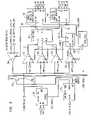
- FIG. 4A further embodiment of single-pin interface of the invention extended to multiple two-bit word transfers is illustrated schematically in FIG. 4 .
- elements common to the embodiment illustrated in FIG. 2maintain the same reference numbers as in FIG. 2 .
- a Register Bank 420is added to the TIA to hold multiple words. Multiple words are transferred by assigning each word to a time slot in the Laser Driver.
- the Master Timer 408(corresponding essentially to the TIA Timer of the prior embodiment) operates to maintain the TIA in the listen mode while the Laser Driver sends rate setting words to the TIA.
- the timing duration for Master Timer 408is longer than one time slot of the Laser Driver Rate Write Timer.
- the Data Timer 410clocks the received and decoded rate setting data into the Register Bank 420 after waiting long enough for the data to be valid.
- the timing duration for TIA Data Timer 410is shorter than the time slot for Laser Driver Rate Write Timer 205 .
- the time slot number(first time slot number is 0, second is 1, etc.) is used as the register address the data is stored into.
- the Time Slot Counter 418 of FIG. 4tracks the time slot number.
- the Time Slot Counteris synchronized to the Laser Driver Rate_Write input signal at the start of the transfer sequence.
- Time Slot Counter 418adds the capability of programming only the first x registers out of N in the TIA while leaving the contents of the N-x remaining registers unchanged. This feature is useful when all the register locations are programmed after power up and only a few settings need to be changed on an on-going basis.
- FIG. 5showing rate-setting timing sequences, in conjunction with FIG. 4 .
- the time axis in FIG. 5is in arbitrary units.
- the description followingbegins with the Laser Driver is operating in the receive mode and then details the operation of the invention to reverse the direction of signal flow on the single line interface so as to place the TIA into its listen mode.
- the process by which the multiple word transfers of this embodiment is carried outis now described.
- the Laser Driverstarts a TIA transfer sequence by pulsing the Rate Write input line to Rate Write Timer 205 (corresponding to the VRTE_WRT timing signal in FIG. 5 ).
- the Write_Initiate signal line from the Rate Write Timer to Switch 209goes low (corresponding to the VWRT INT timing signal of FIG. 5 ), causing Switch 209 to be turned on, thereby causing the LD_TIA Single-Conductor Interface line 201 to be pulled up to the supply voltage level, VCC.
- the Master Timer 408 and the Data Timer 410are reset by the READ_E signal going high.
- the READ_E signalalso clocks the rising edge triggered Time Slot Counter 418 . As described below, the counter is reset only at the start of the transfer sequence.
- the Master Timer CE output(COMP_E signal) is normally in the low state when the TIA is in its normal mode—i.e., sending receive optical signal strength to the Laser Driver.
- the timeris reset, forcing CE high. Note that, although the READ_E signal cycles between high and low states during the multiple time slots (as explained below), CE remains high for more than one time slot independent of the state of the READ_E signal—as a function of timer operation and of retriggering the master timer (by READ_E going high) at start of new time slot.
- the Data Comparators 210 , 212 and 214are turned on by the COMP_E signal (CE output) going high (corresponding to the VCOMP_E timing signal in FIG. 5 ).
- the BUFF_E output signal from Master Timer 408(corresponding to the VBUFF_E timing signal in FIG. 5 ) goes low to disable the Low Output Drive Buffer 204 .
- the Master Timeris retriggered (reset) by the LD_TIA Single-Conductor Interface line 201 being pulled up to the VCC voltage level at the start of the next Laser Driver time slot.
- the CE output of the Master Timeris low before the first time READ_E goes high (i.e., prior to beginning of first time slot) and returns to the low state after the MASTER TIMER times out upon completion of the data transfer sequence.
- the first time slotis detected by comparing a delayed version of the CE output (output of Delay cell 412 ) with the READ_E signal. The time slot detection process is described more particularly below.
- Inverter 414provides a high input signal to AND Gate 416 by inverting the logic low output from Delay 412 .
- the READ_E signalgoes high (indicating that the Single Conductor Interface line has been pulled up to VCC), but the delayed version of COMP_E at output of Delay 412 is still low (indicating that, at an immediately prior time point, the Master Timer was in an idle state), and thus the Inverter input to AND Gate 416 remains high.
- the high READ_E signalwhich is also provided as an input to AND Gate 416 , causes the output of the AND Gate to go high, which resets Time Slot Counter 418 (corresponding to the start of the first time slot).
- the Master Timer 408drives the COMP_E signal high after the rising READ_E edge.
- the delay time of Delay 412is designed to give enough time for Time Slot Counter 418 to properly reset before AND Gate 416 is disabled by COMP_E going high (and thus the inverted input to the AND Gate going low).
- Time Slot Counter 418is positive edge triggered with asynchronous reset to ensure the counter is in state zero before the data for the first time slot is clocked into Registers 420 .
- the short duration reset pulseis shown by the VCNT_RST trace in FIG. 5 .
- the Rate Write Timer 205sends an enable signal to the Laser Driver DAC 207 after the WRITE_INITIATE signal line goes back high (thus removing the VCC voltage level from the Single Conductor Interface line).
- Laser Driver DAC 207operates to provide an analog representation of the rate0 and rate1 setting for successive two-bit words making up the multiple-word transfer of this embodiment. Those analog representations of the successive words are then transferred from the DAC onto the LD TIA Single-Conductor Interface line 201 in successive time slots—each word being transferred in one time slot.
- the Time Slot Counter 418is not reset for this data-transfer interval since the COMP_E signal remains high from the initial time slot interval (and, being past the initial delay interval of Delay 412 , the inverter input to AND Gate 416 remains low), thereby disabling the Time Slot Counter reset path.
- the Time Slot Countertoggles from state zero to state one on the rising READ_E edge.
- the processing of data on the Single Conductor Interface line for this time slotthen proceeds as described for the first time slot.
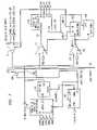
- FIG. 6A still further illustrative embodiment of single-pin interface of the invention for providing a simplified 2-bit/cycle interface is illustrated schematically in FIG. 6 .
- elements common to the embodiments illustrated in FIGS. 2 or 4maintain the same reference numbers in FIG. 6 .
- the Time Slot Counter and Rate Decode/Register Bank functions of the prior illustrative embodimenthave been replaced with a 4-to-2 Decoder 620 and two Serial-In/Parallel-Out Registers 630 and 640 .
- the even bit positionsare stored in Register 630 and the odd positions in the Register 640 .
- TIAProgramming of the TIA in this embodiment is carried out by the Laser Driver writing (and transferring) enough words to update all the positions in the TIA Registers.
- the TIAis simplified relative to the embodiment of FIG. 4 (i.e., the counter is deleted) at the expense of the system having to rewrite all the TIA register positions if any bit needs to be changed.
- the operation sequence and control timingis the same as for the embodiment described in conjunction with FIG. 4 and will not be repeated here.
- Register 640TABLE 2 End of Time Register 630 Register 640 Slot No. B6 B4 B2 B0 B7 B5 B3 B1 0 D0(0) D1(0) 1 D0(1) D0(0) D1(1) D1(0) 2 D0(2) D0(1) D0(0) D1(2) D1(1) D1(0) 3 D0(3) D0(2) D0(1) D0(0) D1(3) D1(2) D1(1) D1(0)
- FIG. 7A still further illustrative embodiment of single-pin interface of the invention in which the interface is simplified to send only one bit per cycle is illustrated schematically in FIG. 7 .
- multiple bitsare sent in multiple cycles.
- elements common to the embodiments illustrated in FIGS. 2 , 4 or 6maintain the same reference numbers in FIG. 7 .
- a Parallel To Serial Shift Register 709is added to the Laser Driver for this embodiment to hold the bits that are to be sent to the TIA. Note, however, that this Register functions to lighten the load on the Laser Driver System Controller, and can be eliminated if the System Controller sends the data to the Laser Driver DAC one bit at a time
- the DAC 707 of this embodimentis simplified to only two levels (1 bit sent per cycle).
- the TIAis also simplified to have only two Comparators.
- Direction Sense Comparator 206functions in the same manner as the Direction Sense Comparators of the previously-described embodiments—i.e., Comparator 206 detects when Switch 209 pulls the LD TIA Single Conductor Interface Line 201 above the normal operating voltage from the TIA Output Drive Buffer.
- the second TIA Comparator ( 710 )detects the 2-level DAC output.
- the TIA decoding and register functionshave been replaced with a Serial In/Parallel Out Register 720 .
- the TIAdoes not keep track of how many bits were sent. That function will be handled by the system that drives the Laser Driver for this embodiment.
- the TIAis programmed by sending enough bits to update all the locations in the TIA shift register.
- the simplified interface of this embodimentrequires the Laser Driver to resend the full register contents if any bit is changed.
- Basic operation and control timing for this embodimentis the same as for the embodiments described in conjunction with FIGS. 4 and 5 .
Landscapes
- Physics & Mathematics (AREA)
- Electromagnetism (AREA)
- Engineering & Computer Science (AREA)
- Computer Networks & Wireless Communication (AREA)
- Signal Processing (AREA)
- Optics & Photonics (AREA)
- Optical Communication System (AREA)
Abstract
Description
| TABLE 1 | |||||||||
| rate | rate | DAC | rl | rl | rl | r | r | r | |
| 1 | 0 | 1 | 2 | 3 | 0 | 1 | 2 | 3 | |
| 0 | 0 | 0 | 0 | 0 | 0 | 1 | 0 | 0 | 0 |
| 0 | 1 | 1 | 1 | 0 | 0 | 0 | 1 | 0 | 0 |
| 1 | 0 | 2 | 1 | 1 | 0 | 0 | 0 | 1 | 0 |
| 1 | 1 | 3 | 1 | 1 | 1 | 0 | 0 | 0 | 1 |
| TABLE 2 | |||
| End of | Register | 630 | |
| Slot No. | B6 | B4 | B2 | B0 | B7 | B3 | B1 | ||
| 0 | D0(0) | D1(0) | |||||||
| 1 | D0(1) | D0(0) | D1(1) | D1(0) | |||||
| 2 | D0(2) | D0(1) | D0(0) | D1(2) | D1(1) | D1(0) | |||
| 3 | D0(3) | D0(2) | D0(1) | D0(0) | D1(3) | D1(2) | D1(1) | D1(0) | |
Claims (17)
Priority Applications (1)
| Application Number | Priority Date | Filing Date | Title |
|---|---|---|---|
| US10/461,671US7539803B2 (en) | 2003-06-13 | 2003-06-13 | Bi-directional interface for low data rate application |
Applications Claiming Priority (1)
| Application Number | Priority Date | Filing Date | Title |
|---|---|---|---|
| US10/461,671US7539803B2 (en) | 2003-06-13 | 2003-06-13 | Bi-directional interface for low data rate application |
Publications (2)
| Publication Number | Publication Date |
|---|---|
| US20040252078A1 US20040252078A1 (en) | 2004-12-16 |
| US7539803B2true US7539803B2 (en) | 2009-05-26 |
Family
ID=33511307
Family Applications (1)
| Application Number | Title | Priority Date | Filing Date |
|---|---|---|---|
| US10/461,671Expired - Fee RelatedUS7539803B2 (en) | 2003-06-13 | 2003-06-13 | Bi-directional interface for low data rate application |
Country Status (1)
| Country | Link |
|---|---|
| US (1) | US7539803B2 (en) |
Cited By (2)
| Publication number | Priority date | Publication date | Assignee | Title |
|---|---|---|---|---|
| US20110022753A1 (en)* | 2009-07-22 | 2011-01-27 | Proton World International N.V. | Single-wire bus communication protocol |
| US10476583B2 (en) | 2015-08-13 | 2019-11-12 | Viasat, Inc. | Managed time division duplexed baseband signaling |
Families Citing this family (5)
| Publication number | Priority date | Publication date | Assignee | Title |
|---|---|---|---|---|
| US7782240B2 (en)* | 2007-05-29 | 2010-08-24 | Atmel Corporation | Device and method of supplying power to targets on single-wire interface |
| US8137003B2 (en)* | 2008-08-12 | 2012-03-20 | Verizon Patent And Licensing Inc. | Dummy connector for a fiber optic cable |
| EP3436858A4 (en)* | 2016-04-01 | 2019-12-04 | Commscope Technologies LLC | FIBER OUTPUT AND HYBRID ELECTRIC |
| CN108694144B (en)* | 2017-04-07 | 2021-08-03 | 苏州倍昊电子科技有限公司 | Interface circuit, signal transmission system and signal transmission method thereof |
| CN113611245B (en)* | 2021-08-17 | 2022-08-26 | 深圳市绿源半导体技术有限公司 | Bidirectional transmission device and control method |
Citations (12)
| Publication number | Priority date | Publication date | Assignee | Title |
|---|---|---|---|---|
| US3993867A (en)* | 1974-10-15 | 1976-11-23 | Motorola, Inc. | Digital single signal line full duplex method and apparatus |
| US4556958A (en)* | 1980-05-30 | 1985-12-03 | Compagnie International Pour L'informatique Cii-Honeywell Bull (Societe Anonyme) | Device for single line bidirectional data transmission between an intelligent card's microprocessor and a second processor |
| US5210846A (en)* | 1989-05-15 | 1993-05-11 | Dallas Semiconductor Corporation | One-wire bus architecture |
| DE10003705A1 (en)* | 2000-01-28 | 2001-08-09 | Siemens Ag | Digital and bidirectional data transmission arrangement e.g. for private motor vehicle electric windows - uses bidirectional single-wire interface between transceiver units, interface being provided with third signal level to enable data interruption without requiring extra control line |
| US20010028297A1 (en)* | 2000-02-21 | 2001-10-11 | Omron Corporation | Control apparatus and control method |
| US20010030617A1 (en)* | 1998-04-13 | 2001-10-18 | Cusey James P. | One-wire device with A-to-D converter |
| US20030023777A1 (en)* | 2001-07-27 | 2003-01-30 | Ken Fields | Dynamic address assignment for one-wire interface |
| US20030035328A1 (en)* | 2001-08-08 | 2003-02-20 | Mitsubishi Denki Kabushiki Kaisha | Semiconductor memory device shiftable to test mode in module as well as semiconductor memory module using the same |
| US20030164752A1 (en)* | 2000-04-28 | 2003-09-04 | Yosef Haimovitch | Apparatus and methods for cellular communication |
| US6697897B1 (en)* | 1999-10-28 | 2004-02-24 | Microchip Technology Incorporated | Data communication interface between host and slave processors |
| US6831925B1 (en)* | 1999-04-06 | 2004-12-14 | National Semiconductor Corporation | Single wire interface with collision detection |
| US6934779B1 (en)* | 2003-04-21 | 2005-08-23 | National Semiconductor Corporation | Analog signal interface for digital control |
Family Cites Families (47)
| Publication number | Priority date | Publication date | Assignee | Title |
|---|---|---|---|---|
| US4712179A (en)* | 1984-08-15 | 1987-12-08 | Cordis Corporation | Method and apparatus for calibrating internal measurements of an implanted cardiac pacer |
| US4825869A (en)* | 1987-09-28 | 1989-05-02 | Telectronics N.V. | System for automatically performing a clinical assessment of an implanted pacer based on information that is telemetrically received |
| US4809697A (en)* | 1987-10-14 | 1989-03-07 | Siemens-Pacesetter, Inc. | Interactive programming and diagnostic system for use with implantable pacemaker |
| USRE38119E1 (en)* | 1989-01-23 | 2003-05-20 | Mirowski Family Ventures, LLC | Method and apparatus for treating hemodynamic disfunction |
| US5097831A (en)* | 1990-04-16 | 1992-03-24 | Siemens-Pacesetter, Inc. | Rate-responsive pacemaker with circuitry for processing multiple sensor inputs |
| US5321618A (en)* | 1990-05-29 | 1994-06-14 | Lawrence Gessman | Apparatus and method for remotely monitoring implanted cardioverter defibrillators |
| US5251626A (en)* | 1990-07-03 | 1993-10-12 | Telectronics Pacing Systems, Inc. | Apparatus and method for the detection and treatment of arrhythmias using a neural network |
| US5226413A (en)* | 1990-08-14 | 1993-07-13 | Medtronic, Inc. | Rate responsive pacemaker and method for automatically initializing the same |
| US5174289A (en)* | 1990-09-07 | 1992-12-29 | Cohen Fred M | Pacing systems and methods for control of the ventricular activation sequence |
| US5292341A (en)* | 1992-03-02 | 1994-03-08 | Siemens Pacesetter, Inc. | Method and system for determining and automatically adjusting the sensor parameters of a rate-responsive pacemaker |
| US5282838A (en)* | 1992-06-08 | 1994-02-01 | Cardiac Pacemakers, Inc. | Dual chamber cardiac pacemaker employing hysteresis to maximize the number of normally conducted ventricular beats with an optimum A-V delay for paced ventricular beats |
| US6168563B1 (en)* | 1992-11-17 | 2001-01-02 | Health Hero Network, Inc. | Remote health monitoring and maintenance system |
| US5372607A (en)* | 1993-06-23 | 1994-12-13 | Medtronic, Inc. | Method and apparatus for monitoring pacemaker intervals |
| US5421830A (en)* | 1993-08-27 | 1995-06-06 | Pacesetter, Inc. | Programming system having means for recording and analyzing a patient's cardiac signal |
| US5594638A (en)* | 1993-12-29 | 1997-01-14 | First Opinion Corporation | Computerized medical diagnostic system including re-enter function and sensitivity factors |
| US5549654A (en)* | 1994-04-15 | 1996-08-27 | Medtronic, Inc. | Interactive interpretation of event markers in body-implantable medical device |
| US5540727A (en)* | 1994-11-15 | 1996-07-30 | Cardiac Pacemakers, Inc. | Method and apparatus to automatically optimize the pacing mode and pacing cycle parameters of a dual chamber pacemaker |
| EP0730882A3 (en)* | 1995-03-08 | 1997-08-06 | Telectronics Nv | An improved implantable cardiac stimulation system |
| US5630835A (en)* | 1995-07-24 | 1997-05-20 | Cardiac Control Systems, Inc. | Method and apparatus for the suppression of far-field interference signals for implantable device data transmission systems |
| US5720771A (en)* | 1995-08-02 | 1998-02-24 | Pacesetter, Inc. | Method and apparatus for monitoring physiological data from an implantable medical device |
| US5716382A (en)* | 1995-08-02 | 1998-02-10 | Pacesetter, Inc. | Programmer for an implantable cardiac stimulating device |
| FR2744817B1 (en)* | 1996-02-08 | 1998-04-03 | Ela Medical Sa | ACTIVE IMPLANTABLE MEDICAL DEVICE AND ITS EXTERNAL PROGRAMMER WITH AUTOMATIC SOFTWARE UPDATE |
| US5607460A (en)* | 1996-03-15 | 1997-03-04 | Angeion Corporation | Physician interface expert system for programming implantable arrythmia treatment devices |
| US5891178A (en)* | 1996-05-14 | 1999-04-06 | Pacesetter, Inc. | Programmer system and associated methods for rapidly evaluating and programming an implanted cardiac device |
| US5833623A (en)* | 1996-05-14 | 1998-11-10 | Pacesetter, Inc. | System and method for facilitating rapid retrieval and evaluation of diagnostic data stored by an implantable medical device |
| US6411847B1 (en)* | 1996-08-19 | 2002-06-25 | Morton M. Mower | Apparatus for applying cyclic pacing at an average rate just above the intrinsic heart rate |
| US5860918A (en)* | 1996-11-22 | 1999-01-19 | Hewlett-Packard Company | Representation of a review of a patent's physiological parameters |
| US6016442A (en)* | 1998-03-25 | 2000-01-18 | Cardiac Pacemakers, Inc. | System for displaying cardiac arrhythmia data |
| US6122545A (en)* | 1998-04-28 | 2000-09-19 | Medtronic, Inc. | Multiple channel sequential cardiac pacing method |
| US6045513A (en)* | 1998-05-13 | 2000-04-04 | Medtronic, Inc. | Implantable medical device for tracking patient functional status |
| US6304773B1 (en)* | 1998-05-21 | 2001-10-16 | Medtronic Physio-Control Manufacturing Corp. | Automatic detection and reporting of cardiac asystole |
| US6190324B1 (en)* | 1999-04-28 | 2001-02-20 | Medtronic, Inc. | Implantable medical device for tracking patient cardiac status |
| US6312378B1 (en)* | 1999-06-03 | 2001-11-06 | Cardiac Intelligence Corporation | System and method for automated collection and analysis of patient information retrieved from an implantable medical device for remote patient care |
| US6272377B1 (en)* | 1999-10-01 | 2001-08-07 | Cardiac Pacemakers, Inc. | Cardiac rhythm management system with arrhythmia prediction and prevention |
| US6351675B1 (en)* | 1999-10-04 | 2002-02-26 | Medtronic, Inc. | System and method of programming an implantable medical device |
| US6442433B1 (en)* | 1999-10-26 | 2002-08-27 | Medtronic, Inc. | Apparatus and method for remote troubleshooting, maintenance and upgrade of implantable device systems |
| US6275727B1 (en)* | 1999-11-04 | 2001-08-14 | Cardiac Pacemakers, Inc. | Implantable cardiac rhythm management device for assessing status of CHF patients |
| US6440066B1 (en)* | 1999-11-16 | 2002-08-27 | Cardiac Intelligence Corporation | Automated collection and analysis patient care system and method for ordering and prioritizing multiple health disorders to identify an index disorder |
| US6368284B1 (en)* | 1999-11-16 | 2002-04-09 | Cardiac Intelligence Corporation | Automated collection and analysis patient care system and method for diagnosing and monitoring myocardial ischemia and outcomes thereof |
| US6411840B1 (en)* | 1999-11-16 | 2002-06-25 | Cardiac Intelligence Corporation | Automated collection and analysis patient care system and method for diagnosing and monitoring the outcomes of atrial fibrillation |
| US6336903B1 (en)* | 1999-11-16 | 2002-01-08 | Cardiac Intelligence Corp. | Automated collection and analysis patient care system and method for diagnosing and monitoring congestive heart failure and outcomes thereof |
| US6398728B1 (en)* | 1999-11-16 | 2002-06-04 | Cardiac Intelligence Corporation | Automated collection and analysis patient care system and method for diagnosing and monitoring respiratory insufficiency and outcomes thereof |
| US20020026223A1 (en)* | 1999-12-24 | 2002-02-28 | Riff Kenneth M. | Method and a system for using implanted medical device data for accessing therapies |
| US6383136B1 (en)* | 2000-03-06 | 2002-05-07 | Charlyn Jordan | Health analysis and forecast of abnormal conditions |
| US6438407B1 (en)* | 2000-03-20 | 2002-08-20 | Medtronic, Inc. | Method and apparatus for monitoring physiologic parameters conjunction with a treatment |
| EP1294441A2 (en)* | 2000-06-14 | 2003-03-26 | Medtronic, Inc. | Deep computing applications in medical device systems |
| WO2002034331A2 (en)* | 2000-10-26 | 2002-05-02 | Medtronic, Inc. | Externally worn transceiver for use with an implantable medical device |
- 2003
- 2003-06-13USUS10/461,671patent/US7539803B2/ennot_activeExpired - Fee Related
Patent Citations (13)
| Publication number | Priority date | Publication date | Assignee | Title |
|---|---|---|---|---|
| US3993867A (en)* | 1974-10-15 | 1976-11-23 | Motorola, Inc. | Digital single signal line full duplex method and apparatus |
| US4556958A (en)* | 1980-05-30 | 1985-12-03 | Compagnie International Pour L'informatique Cii-Honeywell Bull (Societe Anonyme) | Device for single line bidirectional data transmission between an intelligent card's microprocessor and a second processor |
| US5210846A (en)* | 1989-05-15 | 1993-05-11 | Dallas Semiconductor Corporation | One-wire bus architecture |
| US5210846B1 (en)* | 1989-05-15 | 1999-06-29 | Dallas Semiconductor | One-wire bus architecture |
| US20010030617A1 (en)* | 1998-04-13 | 2001-10-18 | Cusey James P. | One-wire device with A-to-D converter |
| US6831925B1 (en)* | 1999-04-06 | 2004-12-14 | National Semiconductor Corporation | Single wire interface with collision detection |
| US6697897B1 (en)* | 1999-10-28 | 2004-02-24 | Microchip Technology Incorporated | Data communication interface between host and slave processors |
| DE10003705A1 (en)* | 2000-01-28 | 2001-08-09 | Siemens Ag | Digital and bidirectional data transmission arrangement e.g. for private motor vehicle electric windows - uses bidirectional single-wire interface between transceiver units, interface being provided with third signal level to enable data interruption without requiring extra control line |
| US20010028297A1 (en)* | 2000-02-21 | 2001-10-11 | Omron Corporation | Control apparatus and control method |
| US20030164752A1 (en)* | 2000-04-28 | 2003-09-04 | Yosef Haimovitch | Apparatus and methods for cellular communication |
| US20030023777A1 (en)* | 2001-07-27 | 2003-01-30 | Ken Fields | Dynamic address assignment for one-wire interface |
| US20030035328A1 (en)* | 2001-08-08 | 2003-02-20 | Mitsubishi Denki Kabushiki Kaisha | Semiconductor memory device shiftable to test mode in module as well as semiconductor memory module using the same |
| US6934779B1 (en)* | 2003-04-21 | 2005-08-23 | National Semiconductor Corporation | Analog signal interface for digital control |
Non-Patent Citations (5)
| Title |
|---|
| "Guidelines for Reliable 1-Wire Networks". Application Note 148. Dallas Semiconductor. Nov. 16, 2001.* |
| "Ultra Reliable 1-Wire Communications". Application Note 159. Dallas Semiconductor. Feb. 4, 2002.* |
| "Using a UART to Implement a 1-Wire Bus Master". Application Note 214. Dallas Semiconductor. Sep. 9, 2002.* |
| "Using the DS2480B Serial 1-Wire Line Driver". Application Note 192. Dallas Semiconductor. Mar. 12, 2002.* |
| Awtrey, Dan. "Transmitting Data and Power over a One-Wire Bus". Sensors-The Journal of Applied Sensing Technology. Feb. 1997.* |
Cited By (3)
| Publication number | Priority date | Publication date | Assignee | Title |
|---|---|---|---|---|
| US20110022753A1 (en)* | 2009-07-22 | 2011-01-27 | Proton World International N.V. | Single-wire bus communication protocol |
| US8683101B2 (en)* | 2009-07-22 | 2014-03-25 | Proton World International N.V. | Single wire bus communication protocol |
| US10476583B2 (en) | 2015-08-13 | 2019-11-12 | Viasat, Inc. | Managed time division duplexed baseband signaling |
Also Published As
| Publication number | Publication date |
|---|---|
| US20040252078A1 (en) | 2004-12-16 |
Similar Documents
| Publication | Publication Date | Title |
|---|---|---|
| US11333907B2 (en) | Optical engine | |
| US8499103B2 (en) | Converter device to convert between different small form factor pluggable standards | |
| KR102710020B1 (en) | Sink Power Optical Data Interconnect System | |
| US7769297B2 (en) | Driving multiple transceiver modules with a single SERDES transceiver chip | |
| KR20210148147A (en) | Battery triggering for activation of optical data interconnection systems | |
| US9294290B2 (en) | Optical cable assemblies with low-speed data pass-through architecture and sleep mode operation | |
| US8595583B2 (en) | System and method for achieving greater than 10 Gbit/s transmission rates for twisted pair physical layer devices | |
| EP0417072A1 (en) | An encoder/decoder system and methodology utilizing conservative coding with block delimiters, for serial communication | |
| US20110106997A1 (en) | Methods and apparatus for interconnecting sas/sata devices using either electrical or optical transceivers | |
| EP1978656A1 (en) | Fiber optic link for transmission of digital data | |
| US20160020856A1 (en) | Optical engines and optical cable assemblies capable of low-speed and high-speed optical communication | |
| US8180935B2 (en) | Methods and apparatus for interconnecting SAS devices using either electrical or optical transceivers | |
| US7539803B2 (en) | Bi-directional interface for low data rate application | |
| EP2996267B1 (en) | Optical engines and optical cable assemblies having electrical signal conditioning | |
| US10566714B2 (en) | High-density small form-factor pluggable module, housing, and system | |
| US11563494B2 (en) | Optical network apparatus and optical module | |
| US7516237B2 (en) | Scalable device-to-device interconnection | |
| CN112567650B (en) | Optical Engine | |
| US7522641B2 (en) | Ten gigabit copper physical layer system | |
| US20250219741A1 (en) | Photoreceiver circuit, photodetector, photodetector array and optical receiver unit | |
| CN113747278A (en) | FPGA-based hundred-million-light physical layer and device thereof | |
| KR20030061936A (en) | Multimedia Multiplexing Transmition System | |
| WO2025146108A1 (en) | Data transmission system, device and method | |
| WO2025153186A1 (en) | Extender phy transceiver architecture | |
| JPH0233246A (en) | Digital signal transmission method |
Legal Events
| Date | Code | Title | Description |
|---|---|---|---|
| AS | Assignment | Owner name:AGERE SYSTEMS INC., PENNSYLVANIA Free format text:ASSIGNMENT OF ASSIGNORS INTEREST;ASSIGNORS:FISCHER, JONATHAN H.;SOTO, WALTER G.;REEL/FRAME:014189/0342;SIGNING DATES FROM 20030609 TO 20030612 | |
| STCF | Information on status: patent grant | Free format text:PATENTED CASE | |
| FPAY | Fee payment | Year of fee payment:4 | |
| AS | Assignment | Owner name:DEUTSCHE BANK AG NEW YORK BRANCH, AS COLLATERAL AG Free format text:PATENT SECURITY AGREEMENT;ASSIGNORS:LSI CORPORATION;AGERE SYSTEMS LLC;REEL/FRAME:032856/0031 Effective date:20140506 | |
| AS | Assignment | Owner name:AVAGO TECHNOLOGIES GENERAL IP (SINGAPORE) PTE. LTD Free format text:ASSIGNMENT OF ASSIGNORS INTEREST;ASSIGNOR:AGERE SYSTEMS LLC;REEL/FRAME:035365/0634 Effective date:20140804 | |
| AS | Assignment | Owner name:LSI CORPORATION, CALIFORNIA Free format text:TERMINATION AND RELEASE OF SECURITY INTEREST IN PATENT RIGHTS (RELEASES RF 032856-0031);ASSIGNOR:DEUTSCHE BANK AG NEW YORK BRANCH, AS COLLATERAL AGENT;REEL/FRAME:037684/0039 Effective date:20160201 Owner name:AGERE SYSTEMS LLC, PENNSYLVANIA Free format text:TERMINATION AND RELEASE OF SECURITY INTEREST IN PATENT RIGHTS (RELEASES RF 032856-0031);ASSIGNOR:DEUTSCHE BANK AG NEW YORK BRANCH, AS COLLATERAL AGENT;REEL/FRAME:037684/0039 Effective date:20160201 | |
| AS | Assignment | Owner name:BANK OF AMERICA, N.A., AS COLLATERAL AGENT, NORTH CAROLINA Free format text:PATENT SECURITY AGREEMENT;ASSIGNOR:AVAGO TECHNOLOGIES GENERAL IP (SINGAPORE) PTE. LTD.;REEL/FRAME:037808/0001 Effective date:20160201 Owner name:BANK OF AMERICA, N.A., AS COLLATERAL AGENT, NORTH Free format text:PATENT SECURITY AGREEMENT;ASSIGNOR:AVAGO TECHNOLOGIES GENERAL IP (SINGAPORE) PTE. LTD.;REEL/FRAME:037808/0001 Effective date:20160201 | |
| FPAY | Fee payment | Year of fee payment:8 | |
| AS | Assignment | Owner name:AVAGO TECHNOLOGIES GENERAL IP (SINGAPORE) PTE. LTD., SINGAPORE Free format text:TERMINATION AND RELEASE OF SECURITY INTEREST IN PATENTS;ASSIGNOR:BANK OF AMERICA, N.A., AS COLLATERAL AGENT;REEL/FRAME:041710/0001 Effective date:20170119 Owner name:AVAGO TECHNOLOGIES GENERAL IP (SINGAPORE) PTE. LTD Free format text:TERMINATION AND RELEASE OF SECURITY INTEREST IN PATENTS;ASSIGNOR:BANK OF AMERICA, N.A., AS COLLATERAL AGENT;REEL/FRAME:041710/0001 Effective date:20170119 | |
| AS | Assignment | Owner name:AVAGO TECHNOLOGIES INTERNATIONAL SALES PTE. LIMITE Free format text:MERGER;ASSIGNOR:AVAGO TECHNOLOGIES GENERAL IP (SINGAPORE) PTE. LTD.;REEL/FRAME:047195/0827 Effective date:20180509 | |
| AS | Assignment | Owner name:AVAGO TECHNOLOGIES INTERNATIONAL SALES PTE. LIMITE Free format text:CORRECTIVE ASSIGNMENT TO CORRECT THE EFFECTIVE DATE OF MERGER PREVIOUSLY RECORDED AT REEL: 047195 FRAME: 0827. ASSIGNOR(S) HEREBY CONFIRMS THE MERGER;ASSIGNOR:AVAGO TECHNOLOGIES GENERAL IP (SINGAPORE) PTE. LTD.;REEL/FRAME:047924/0571 Effective date:20180905 | |
| FEPP | Fee payment procedure | Free format text:MAINTENANCE FEE REMINDER MAILED (ORIGINAL EVENT CODE: REM.); ENTITY STATUS OF PATENT OWNER: LARGE ENTITY | |
| LAPS | Lapse for failure to pay maintenance fees | Free format text:PATENT EXPIRED FOR FAILURE TO PAY MAINTENANCE FEES (ORIGINAL EVENT CODE: EXP.); ENTITY STATUS OF PATENT OWNER: LARGE ENTITY | |
| STCH | Information on status: patent discontinuation | Free format text:PATENT EXPIRED DUE TO NONPAYMENT OF MAINTENANCE FEES UNDER 37 CFR 1.362 | |
| FP | Lapsed due to failure to pay maintenance fee | Effective date:20210526 |