US7539366B1 - Optical transceiver module - Google Patents
Optical transceiver moduleDownload PDFInfo
- Publication number
- US7539366B1 US7539366B1US11/969,374US96937408AUS7539366B1US 7539366 B1US7539366 B1US 7539366B1US 96937408 AUS96937408 AUS 96937408AUS 7539366 B1US7539366 B1US 7539366B1
- Authority
- US
- United States
- Prior art keywords
- array
- chip
- opto
- optical module
- integrated circuit
- Prior art date
- Legal status (The legal status is an assumption and is not a legal conclusion. Google has not performed a legal analysis and makes no representation as to the accuracy of the status listed.)
- Expired - Fee Related
Links
- 230000003287optical effectEffects0.000titleclaimsabstractdescription54
- 230000005693optoelectronicsEffects0.000claimsabstractdescription68
- 239000000758substrateSubstances0.000claimsdescription16
- 239000013307optical fiberSubstances0.000claimsdescription5
- VYPSYNLAJGMNEJ-UHFFFAOYSA-NSilicium dioxideChemical compoundO=[Si]=OVYPSYNLAJGMNEJ-UHFFFAOYSA-N0.000claimsdescription2
- 239000005350fused silica glassSubstances0.000claimsdescription2
- 239000011521glassSubstances0.000claimsdescription2
- BWWVXHRLMPBDCK-UHFFFAOYSA-N1,2,4-trichloro-5-(2,6-dichlorophenyl)benzeneChemical compoundC1=C(Cl)C(Cl)=CC(Cl)=C1C1=C(Cl)C=CC=C1ClBWWVXHRLMPBDCK-UHFFFAOYSA-N0.000description20
- 238000010586diagramMethods0.000description15
- 238000013461designMethods0.000description6
- 238000003491arrayMethods0.000description5
- JBRZTFJDHDCESZ-UHFFFAOYSA-NAsGaChemical compound[As]#[Ga]JBRZTFJDHDCESZ-UHFFFAOYSA-N0.000description4
- 238000004806packaging method and processMethods0.000description4
- 229910001218Gallium arsenideInorganic materials0.000description3
- 230000008878couplingEffects0.000description3
- 238000010168coupling processMethods0.000description3
- 238000005859coupling reactionMethods0.000description3
- 238000005516engineering processMethods0.000description3
- 238000012986modificationMethods0.000description3
- 230000004048modificationEffects0.000description3
- 238000004519manufacturing processMethods0.000description2
- 230000003071parasitic effectEffects0.000description2
- 239000004065semiconductorSubstances0.000description2
- JMASRVWKEDWRBT-UHFFFAOYSA-NGallium nitrideChemical compound[Ga]#NJMASRVWKEDWRBT-UHFFFAOYSA-N0.000description1
- -1InPChemical compound0.000description1
- XUIMIQQOPSSXEZ-UHFFFAOYSA-NSiliconChemical compound[Si]XUIMIQQOPSSXEZ-UHFFFAOYSA-N0.000description1
- 239000000853adhesiveSubstances0.000description1
- 230000001070adhesive effectEffects0.000description1
- 230000002411adverseEffects0.000description1
- 238000013459approachMethods0.000description1
- 230000009286beneficial effectEffects0.000description1
- 239000000969carrierSubstances0.000description1
- 239000000919ceramicSubstances0.000description1
- 238000004891communicationMethods0.000description1
- 230000000295complement effectEffects0.000description1
- 230000007123defenseEffects0.000description1
- 239000000835fiberSubstances0.000description1
- PCHJSUWPFVWCPO-UHFFFAOYSA-NgoldChemical compound[Au]PCHJSUWPFVWCPO-UHFFFAOYSA-N0.000description1
- 229910052737goldInorganic materials0.000description1
- 239000010931goldSubstances0.000description1
- 238000010438heat treatmentMethods0.000description1
- 229910052738indiumInorganic materials0.000description1
- APFVFJFRJDLVQX-UHFFFAOYSA-Nindium atomChemical compound[In]APFVFJFRJDLVQX-UHFFFAOYSA-N0.000description1
- 230000001788irregularEffects0.000description1
- 238000000034methodMethods0.000description1
- 238000012536packaging technologyMethods0.000description1
- 239000004033plasticSubstances0.000description1
- 229920003023plasticPolymers0.000description1
- 230000008569processEffects0.000description1
- 238000012545processingMethods0.000description1
- 238000011160researchMethods0.000description1
- 229910052710siliconInorganic materials0.000description1
- 239000010703siliconSubstances0.000description1
- 229910000679solderInorganic materials0.000description1
- 239000007858starting materialSubstances0.000description1
- 239000012780transparent materialSubstances0.000description1
Images


Classifications
- G—PHYSICS
- G02—OPTICS
- G02B—OPTICAL ELEMENTS, SYSTEMS OR APPARATUS
- G02B6/00—Light guides; Structural details of arrangements comprising light guides and other optical elements, e.g. couplings
- G02B6/24—Coupling light guides
- G02B6/42—Coupling light guides with opto-electronic elements
- G02B6/4201—Packages, e.g. shape, construction, internal or external details
- G02B6/4219—Mechanical fixtures for holding or positioning the elements relative to each other in the couplings; Alignment methods for the elements, e.g. measuring or observing methods especially used therefor
- G02B6/4236—Fixing or mounting methods of the aligned elements
- G02B6/4245—Mounting of the opto-electronic elements
- G—PHYSICS
- G02—OPTICS
- G02B—OPTICAL ELEMENTS, SYSTEMS OR APPARATUS
- G02B6/00—Light guides; Structural details of arrangements comprising light guides and other optical elements, e.g. couplings
- G02B6/24—Coupling light guides
- G02B6/42—Coupling light guides with opto-electronic elements
- G02B6/4201—Packages, e.g. shape, construction, internal or external details
- G02B6/4246—Bidirectionally operating package structures
- G—PHYSICS
- G02—OPTICS
- G02B—OPTICAL ELEMENTS, SYSTEMS OR APPARATUS
- G02B6/00—Light guides; Structural details of arrangements comprising light guides and other optical elements, e.g. couplings
- G02B6/24—Coupling light guides
- G02B6/42—Coupling light guides with opto-electronic elements
- G02B6/4201—Packages, e.g. shape, construction, internal or external details
- G02B6/4256—Details of housings
- G02B6/4257—Details of housings having a supporting carrier or a mounting substrate or a mounting plate
- G02B6/4259—Details of housings having a supporting carrier or a mounting substrate or a mounting plate of the transparent type
- G—PHYSICS
- G02—OPTICS
- G02B—OPTICAL ELEMENTS, SYSTEMS OR APPARATUS
- G02B6/00—Light guides; Structural details of arrangements comprising light guides and other optical elements, e.g. couplings
- G02B6/24—Coupling light guides
- G02B6/42—Coupling light guides with opto-electronic elements
- G02B6/4201—Packages, e.g. shape, construction, internal or external details
- G02B6/4256—Details of housings
- G02B6/426—Details of housings mounting, engaging or coupling of the package to a board, a frame or a panel
- G—PHYSICS
- G02—OPTICS
- G02B—OPTICAL ELEMENTS, SYSTEMS OR APPARATUS
- G02B6/00—Light guides; Structural details of arrangements comprising light guides and other optical elements, e.g. couplings
- G02B6/24—Coupling light guides
- G02B6/42—Coupling light guides with opto-electronic elements
- G02B6/4201—Packages, e.g. shape, construction, internal or external details
- G02B6/4274—Electrical aspects
- G02B6/428—Electrical aspects containing printed circuit boards [PCB]
- H—ELECTRICITY
- H05—ELECTRIC TECHNIQUES NOT OTHERWISE PROVIDED FOR
- H05K—PRINTED CIRCUITS; CASINGS OR CONSTRUCTIONAL DETAILS OF ELECTRIC APPARATUS; MANUFACTURE OF ASSEMBLAGES OF ELECTRICAL COMPONENTS
- H05K1/00—Printed circuits
- H05K1/02—Details
- H05K1/0274—Optical details, e.g. printed circuits comprising integral optical means
- H—ELECTRICITY
- H10—SEMICONDUCTOR DEVICES; ELECTRIC SOLID-STATE DEVICES NOT OTHERWISE PROVIDED FOR
- H10F—INORGANIC SEMICONDUCTOR DEVICES SENSITIVE TO INFRARED RADIATION, LIGHT, ELECTROMAGNETIC RADIATION OF SHORTER WAVELENGTH OR CORPUSCULAR RADIATION
- H10F55/00—Radiation-sensitive semiconductor devices covered by groups H10F10/00, H10F19/00 or H10F30/00 being structurally associated with electric light sources and electrically or optically coupled thereto
- H10F55/20—Radiation-sensitive semiconductor devices covered by groups H10F10/00, H10F19/00 or H10F30/00 being structurally associated with electric light sources and electrically or optically coupled thereto wherein the electric light source controls the radiation-sensitive semiconductor devices, e.g. optocouplers
- H10F55/25—Radiation-sensitive semiconductor devices covered by groups H10F10/00, H10F19/00 or H10F30/00 being structurally associated with electric light sources and electrically or optically coupled thereto wherein the electric light source controls the radiation-sensitive semiconductor devices, e.g. optocouplers wherein the radiation-sensitive devices and the electric light source are all semiconductor devices
- H10F55/255—Radiation-sensitive semiconductor devices covered by groups H10F10/00, H10F19/00 or H10F30/00 being structurally associated with electric light sources and electrically or optically coupled thereto wherein the electric light source controls the radiation-sensitive semiconductor devices, e.g. optocouplers wherein the radiation-sensitive devices and the electric light source are all semiconductor devices formed in, or on, a common substrate
- G—PHYSICS
- G02—OPTICS
- G02B—OPTICAL ELEMENTS, SYSTEMS OR APPARATUS
- G02B6/00—Light guides; Structural details of arrangements comprising light guides and other optical elements, e.g. couplings
- G02B6/24—Coupling light guides
- G02B6/42—Coupling light guides with opto-electronic elements
- G02B6/4201—Packages, e.g. shape, construction, internal or external details
- G02B6/4204—Packages, e.g. shape, construction, internal or external details the coupling comprising intermediate optical elements, e.g. lenses, holograms
- H—ELECTRICITY
- H05—ELECTRIC TECHNIQUES NOT OTHERWISE PROVIDED FOR
- H05K—PRINTED CIRCUITS; CASINGS OR CONSTRUCTIONAL DETAILS OF ELECTRIC APPARATUS; MANUFACTURE OF ASSEMBLAGES OF ELECTRICAL COMPONENTS
- H05K1/00—Printed circuits
- H05K1/02—Details
- H05K1/14—Structural association of two or more printed circuits
- H05K1/141—One or more single auxiliary printed circuits mounted on a main printed circuit, e.g. modules, adapters
- H—ELECTRICITY
- H05—ELECTRIC TECHNIQUES NOT OTHERWISE PROVIDED FOR
- H05K—PRINTED CIRCUITS; CASINGS OR CONSTRUCTIONAL DETAILS OF ELECTRIC APPARATUS; MANUFACTURE OF ASSEMBLAGES OF ELECTRICAL COMPONENTS
- H05K1/00—Printed circuits
- H05K1/18—Printed circuits structurally associated with non-printed electric components
- H05K1/182—Printed circuits structurally associated with non-printed electric components associated with components mounted in the printed circuit board, e.g. insert mounted components [IMC]
- H—ELECTRICITY
- H05—ELECTRIC TECHNIQUES NOT OTHERWISE PROVIDED FOR
- H05K—PRINTED CIRCUITS; CASINGS OR CONSTRUCTIONAL DETAILS OF ELECTRIC APPARATUS; MANUFACTURE OF ASSEMBLAGES OF ELECTRICAL COMPONENTS
- H05K2201/00—Indexing scheme relating to printed circuits covered by H05K1/00
- H05K2201/01—Dielectrics
- H05K2201/0104—Properties and characteristics in general
- H05K2201/0108—Transparent
- H—ELECTRICITY
- H05—ELECTRIC TECHNIQUES NOT OTHERWISE PROVIDED FOR
- H05K—PRINTED CIRCUITS; CASINGS OR CONSTRUCTIONAL DETAILS OF ELECTRIC APPARATUS; MANUFACTURE OF ASSEMBLAGES OF ELECTRICAL COMPONENTS
- H05K2201/00—Indexing scheme relating to printed circuits covered by H05K1/00
- H05K2201/09—Shape and layout
- H05K2201/09009—Substrate related
- H05K2201/09036—Recesses or grooves in insulating substrate
- H—ELECTRICITY
- H05—ELECTRIC TECHNIQUES NOT OTHERWISE PROVIDED FOR
- H05K—PRINTED CIRCUITS; CASINGS OR CONSTRUCTIONAL DETAILS OF ELECTRIC APPARATUS; MANUFACTURE OF ASSEMBLAGES OF ELECTRICAL COMPONENTS
- H05K2201/00—Indexing scheme relating to printed circuits covered by H05K1/00
- H05K2201/10—Details of components or other objects attached to or integrated in a printed circuit board
- H05K2201/10007—Types of components
- H05K2201/10121—Optical component, e.g. opto-electronic component
Definitions
- the present inventionrelates generally to an improved data processing system. More specifically, the present invention is directed to an optical transceiver module that utilizes a transparent carrier and one or more integrated circuits, which are attached to both the transparent carrier and a package.
- VCSELsvertical cavity surface emitting lasers
- Current packaging technologyconsists of mounting optoelectronic (OE) arrays and analog amplifier integrated circuits (ICs) in close proximity and then establishing an electrical contact between the OEs and ICs with wire bonds.
- wire bondingmakes packaging two-dimensional (2-D) arrays problematic by precluding the possibility of producing optical transmitters and receivers with a large number of parallel channels, such as, for example, greater than 24.
- Applications that require high communication bandwidthsuch as data buses within computer systems or switches/routers used for telecommunications, require optical modules with a large number of transmitter and receiver channels that are each capable of operating at speeds in excess of ten Gb/s.
- GaAs and InP substrateswhich are typically used as the starting material for producing photodiodes and VCSELs, are not transparent to a wavelength at substantially 850 nanometers (nm).
- This 850 nm wavelengthwhich is an industry standard, is technologically important because low-cost GaAs-based devices may be used for the lasers and detectors.
- 850 nm wavelength optical data linksare commonly utilized by many institutions, agencies, organizations, enterprises, and premises wiring applications that support networks, such as, for example, local area networks (LANs) or storage area networks (SANs).
- optical transceiver modulethat is compact, scalable, and compatible with operation of VCSELs and photodiodes at a wavelength of 850 nm.
- Illustrative embodimentsprovide an improved optical transceiver module.
- the optical transceiver moduleincludes a printed circuit board and an opto-chip.
- the opto-chipincludes a transparent carrier with an optoelectronic device array and an associated integrated circuit array that are flip chip attached to the transparent carrier.
- the optoelectronic device array and the associated integrated circuit arrayare interconnected via surface wiring with bond sites.
- the associated integrated circuit arrayextends beyond the transparent carrier to provide direct flip chip attachment of the opto-chip to the printed circuit board.
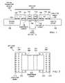
- FIG. 1is a block diagram of a side edge view of an optical transceiver module in which illustrative embodiments may be implemented;
- FIG. 2is a block diagram of a bottom view of an opto-chip in accordance with an illustrative embodiment
- FIG. 3is an exemplary illustration of a top view of a transparent carrier in accordance with an illustrative embodiment
- FIG. 4is an exemplary illustration of a bottom view of a transparent carrier in accordance with an illustrative embodiment
- FIG. 5is a block diagram of a side edge view of a separate transmitter or receiver opto-chip in which illustrative embodiments may be implemented;
- FIG. 6is a block diagram of a bottom view of a separate transmitter or receiver opto-chip in which illustrative embodiments may be implemented;
- FIG. 7is a block diagram of a side edge view of a transceiver opto-chip with one transceiver IC and two OEs in which illustrative embodiments may be implemented;
- FIG. 8is a block diagram of a bottom view of a transceiver opto-chip with one transceiver IC and two OEs in which illustrative embodiments may be implemented;
- FIG. 9is a block diagram of a side edge view of an optical transceiver module with a bottom mounted opto-chip in which illustrative embodiments may be implemented.
- FIG. 1an exemplary block diagram of an optical module apparatus is provided in which illustrative embodiments may be implemented. It should be appreciated that FIG. 1 is only exemplary and is not intended to assert or imply any limitation with regard to different illustrative embodiments. Many modifications to the depicted optical module may be made.
- FIG. 1depicts a block diagram of a side edge view of an optical transceiver module in which illustrative embodiments may be implemented.
- Optical transceiver module 100is an electrical and optical component that is capable of transmitting and receiving pulses of light, which are used to communicate data.
- Optical transceiver module 100includes printed circuit board (PCB) 102 and opto-chip 104 .
- PCBprinted circuit board
- PCB 102mechanically supports and electronically connects electronic components, such as opto-chip 104 , to other electronic components.
- PCB 102may, for example, be an organic carrier, which is similar to conventional chip carriers.
- PCB 102may also be a ceramic carrier.
- PCB 102may include a conventional ball grid array (BGA) of bond pads on its bottom surface for surface mounting to, for example, a motherboard (shown in the illustrative example of FIG. 9 ).
- BGAball grid array
- PBC 102may incorporate other electronic chips, such as, for example, microprocessors or control chips, in addition to opto-chip 104 .
- PCB 102includes an area that is cutout or devoid of structure.
- the cutoutis a square or rectangular area surrounded by PCB 102 on all four sides.
- the cutout areamay be any regular or irregular geometric shape and may not be entirely surrounded by PCB 102 .
- the cutout areamay only be surrounded by PCB 102 on three sides or two sides depending on whether the cutout is on an edge or a corner of PCB 102 .
- PCB 102utilizes the cutout area to accommodate a portion or all of the structure of opto-chip 104 .
- Opto-chip 104is a chip-like device that is flip chip attached to PCB 102 .
- Opto-chip 104includes transparent carrier 106 , IC 1 108 , IC 2 110 , OE 1 112 , and OE 2 114 .
- Transparent carrier 106is a substrate that electronic devices, such as IC 1 108 , IC 2 110 , OE 1 112 , and OE 2 114 may connect to.
- IC 1 108 and IC 2 110extend beyond the dimensions of transparent carrier 106 to provide bond pads for electrical I/O to and from PCB 102 .
- transparent carrier 106is transparent to pulses of light, such as optical I/O 116 .
- transparent carrier 106is made of glass or fused silica.
- transparent carrier 106may be made of any transparent material capable of accomplishing processes of illustrative embodiments.
- transparent carrier 106includes electrical lines (shown in the illustrative example of FIG. 3 ), which provide connectivity between IC 1 108 and OE 1 112 and IC 2 110 and OE 2 114 .
- lensessuch as integrated lenses 118 , may be integrated into transparent carrier 106 to provide more efficient optical coupling between the OEs and optical fibers or optical circuits.
- integrated lenses 118may provide for greater coupling distances between the OEs and the optical fibers or optical circuits by focusing the pulses of light to the OEs.
- Opto-chip 104includes arrays of OE devices, such as, for example, vertical cavity surface emitting lasers (VCSELs) or photodiodes, and ICs, such as, for example, complementary metal-oxide-semiconductor (CMOS) laser drivers or CMOS receiver chips.
- CMOScomplementary metal-oxide-semiconductor
- the ICsmay also be implemented in other circuit technologies, such as, for example, GaAs, InP, silicon (Si) bipolar, or gallium nitride (GaN) technologies. Even though only two OEs and two ICs are shown in this illustrative example, illustrative embodiments are not limited to such. Illustrative embodiments may include more or fewer OEs and ICs as needed by alternative illustrative embodiments.
- OE 1 112is a VCSEL.
- opto-chip 104uses OE 1 112 as a transmitter to output pulses of light.
- IC 1 108is a laser driver, such as, for example, a CMOS laser driver.
- Opto-chip 104uses IC 1 108 to modulate the output of light pulses to represent ones and zeros for communicating data.
- OE 2 114is a photodiode.
- opto-chip 104uses OE 2 114 to receive light pulses as input.
- IC 2 110is a receiver chip, such as, for example, a CMOS receiver chip, that converts the received light pulses into electrical signals.
- IC 1 108 , IC 2 110 , OE 1 112 , and OE 2 114are flip chip attached to transparent carrier 106 .
- Flip chipoffers increased high speed electrical performance.
- Flip chipis one type of mounting used for semiconductor devices, such as ICs and OEs, which does not require any wire bonds. Eliminating bond wires may reduce the delaying inductance and capacitance of a connection by a factor of ten and may shorten an electrical path by a factor of 25 to 100. The result is a higher speed interconnection.
- Conductive bumps 120may, for example, be solder bumps, gold balls, molded studs, or electrically conductive plastics. Conductive bumps 120 connect directly to the associated external circuitry. This type of mounting is also known as the Controlled Collapse Chip Connection, or C4. Also, this type of mounting leaves a small space between the chip's circuitry and the underlying substrate or mounting.
- An electrically-insulating adhesivemay be “under filled” in this small space to provide a stronger mechanical connection, provide a heat bridge, and to ensure conductive bumps 120 are not stressed due to differential heating of opto-chip 104 and PCB 102 .
- the resulting completed assemblyi.e., optical transceiver module 100
- optical transceiver module 100is much smaller than a traditional carrier-based system, both in terms of area and height, because opto-chip 104 sits directly on PCB 102 .
- illustrative embodimentsprovide very short electrical traces between the OEs and ICs on the transparent substrate, while simultaneously enabling the direct flip chip attachment of the resulting opto-chip assembly directly to a PCB or flex circuit.
- This aspect of the inventionallows the optical transceiver module to be attached to a circuit board in a manner similar to that employed for electronic components in high-volume, low-cost, surface-mount board technologies.
- the exclusive use of flip chip packagingallows the complete assembly to operate at high speeds, such as, for example, greater than ten Gb/s, with a high density of integrated channels.
- illustrative embodimentsprovide low-cost, small-footprint, parallel optical transmitters, receivers, or transceivers based on 850 nm wavelength OE devices.
- the exclusive use of flip chip packaging to attach both the amplifier and OE chips to a transparent substrateminimizes the footprint of the assembled module, as well as the parasitic inductance and capacitance incurred in the connections between chips. This allows the production of optical modules with many parallel channels and also maximizes the speed that may be obtained for each individual channel.
- Opto-chip 200may, for example, be opto-chip 104 in FIG. 1 .
- Opto-chip 200includes transparent carrier 202 , IC 1 204 , IC 2 206 , OE 1 208 , and OE 2 210 , such as, for example, transparent carrier 106 , IC 1 108 , IC 2 110 , OE 1 112 , and OE 2 114 in FIG. 1 .
- opto-chip 200 in this illustrative exampleis being viewed from the underside.
- Conductive bumps 212 for IC 1 204 and IC 2 206 that connect opto-chip 200 to a PCB, such as PCB 102 in FIG. 1are visible.
- Conductive bumps 212may, for example, be conductive bumps 120 in FIG. 1 .
- Transparent carrier 300may, for example, be transparent carrier 106 in FIG. 1 .
- Transparent carrier 300includes IC 1 bond sites 302 , IC 2 bond sites 304 , OE 1 bond sites 306 , and OE 2 bond sites 308 .
- IC 1 bond sites 302 and IC 2 bond sites 304provide the bonding sites for ICs, such as IC 1 108 and IC 2 110 in FIG. 1 , to transparent carrier 300 .
- the ICsconnect to transparent carrier 300 via conductive bumps, such as conductive bumps 120 in FIG. 1 , which are positioned over the bond sites and then re-melted.
- OE 1 bond sites 306 and OE 2 bond sites 308provide the bonding sites for OEs, such as OE 1 112 and OE 2 114 in FIG. 1 , to transparent carrier 300 .
- the OEsconnect to transparent carrier 300 via conductive bumps as well.
- IC 1 bond sites 302 and OE 1 bond sites 306are electrically connected via interconnecting surface wiring 310 .
- IC 2 bond sites 304 and OE 2 bond sites 308are electrically connected via interconnecting surface wiring 312 .
- associated ICs and OEs that are flip chip attached to transparent carrier 300are electrically coupled together.
- Illustrative embodimentsutilize transparent carrier 300 to provide short, high-speed electrical links between ICs, such as CMOS laser drivers or receiver chips, and their associated OEs, such as VCSELs or photodiodes. The I/O between the ICs and the rest of the system are established through direct flip chip attachment to a PCB, such as PCB 102 in FIG. 1 .
- transparent carrier 300may include multi-layered interconnecting wiring between ICs and OEs.
- This multi-layered interconnecting wiringmay allow for IC and OE arrays of, for example, 4 ⁇ 8 or 6 ⁇ 8, instead of just 2 ⁇ 8 as shown in this illustrative example.
- illustrative embodimentsare not limited to only eight rows of ICs and OEs. Illustrative embodiments may utilize any number combination of columns to rows.
- transparent carrier 300includes integrated lenses, such as integrated lens 118 in FIG. 1 , which are depicted as shaded areas around OE 1 bond sites 306 and OE 2 bond sites 308 .
- the integrated lensesare located on the bottom side of transparent carrier 300 .
- Transparent carrier 300uses the integrated lenses to focus light pulses, such as optical I/O 116 in FIG. 1 , to the OEs attached to transparent carrier 300 .
- Transparent carrier 400may, for example, be transparent carrier 300 in FIG. 3 .
- Transparent carrier 400includes integrated lenses 402 and integrated lenses 404 , such as integrated lenses 118 in FIG. 1 , which are integrated into the bottom surface of transparent carrier 400 .
- integrated lenses 402are in a 2 ⁇ 8 array.
- This 2 ⁇ 8 array of lenses shown in this illustrative examplecorresponds to a 2 ⁇ 8 array of OEs flip chip attached to the top surface of transparent carrier 400 .
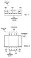
- Opto-chip 500includes transparent carrier 502 , IC 504 , and OE 506 , such as, for example, transparent carrier 106 , IC 1 108 , and OE 1 112 in FIG. 1 .
- opto-chip 500may be used as either a transmitter or a receiver depending upon the type of component flip chip attached to transparent carrier 502 .
- IC 504may be a CMOS laser driver and OE 506 may be a VCSEL, which in this case opto-chip 500 is a transmitter of optical pulses to optical circuits or optical fibers.
- IC 504may be a CMOS receiver chip and OE 506 may be a photodiode, which in this case opto-chip 500 is a receiver of optical pulses from the optical circuits or fibers.
- opto-chip 500may include a 1 ⁇ N array of ICs and OEs.
- Opto-chip 600may, for example, be opto-chip 500 in FIG. 5 .
- Opto-chip 600includes transparent carrier 602 , IC 604 , and OE 606 , such as, for example, transparent carrier 502 , IC 504 , and OE 506 in FIG. 5 .
- This illustrative exampleprovides a bottom side view of opto-chip 600 , which is an opposing view to the illustrative example provided in FIG. 5 .
- Opto-chip 700includes transparent carrier 702 , transceiver IC 704 , OE 1 706 , and OE 2 708 .
- Transparent carrier 702 , OE 1 706 , and OE 2 708may, for example, be transparent carrier 106 , OE 1 108 , and OE 2 110 in FIG. 1 .
- Transceiver IC 704is a single IC that includes both a transmitter, such as a CMOS laser driver, and a receiver, such as a CMOS receiver chip, for OE 1 706 and OE 2 708 .
- Opto-chip 800may, for example, be opto-chip 700 in FIG. 7 .
- Opto-chip 800includes transparent carrier 802 , transceiver IC 804 , OE 1 806 , and OE 2 808 , such as, for example, transparent carrier 702 , transceiver IC 704 , OE 1 706 , and OE 2 708 in FIG. 7 .
- this illustrative exampleshows conductive bumps 810 , such as conductive bumps 208 in FIG. 2 , which are attached to the bottom side of transceiver IC 804 .
- Transceiver IC 804uses conductive bumps 810 to flip chip attach to a PCB, such as, for example, PCB 102 in FIG. 1 .
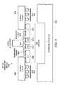
- Optical transceiver module 900may, for example, be optical transceiver module 100 in FIG. 1 .
- Optical transceiver module 900includes PCB 902 and opto-chip 904 , such as, for example, PCB 102 and opto-chip 104 in FIG. 1 .
- opto-chip 904is flip chip attached to the bottom side of PCB 902
- opto-chip 104is flip chip attached to the top side of PCB 102 in FIG. 1 .
- PCB 902includes a cutout area to accommodate a portion of opto-chip 902 .
- Opto-chip 904includes transparent carrier 906 , IC 1 908 , IC 2 910 , OE 1 912 , and OE 2 914 .
- Transparent carrier 906includes integrated lenses 916 , which provide more efficient optical coupling between OE 1 912 and OE 2 914 and optical fibers.
- Optical transceiver module 900also includes BGA 918 .
- BGA 918is an array of bond pads on the bottom surface of PCB 902 for surface mounting to system PCB 920 .
- System PCB 920may, for example, be a motherboard.
- system PCB 920also includes a cutout area to accommodate a portion of bottom mounted opto-chip 904 .
- illustrative embodimentsprovide an improved optical transceiver module.
- the circuit as described aboveis part of the design for an integrated circuit chip.
- the chip designis created in a graphical computer programming language, and stored in a computer storage medium (such as a disk, tape, physical hard drive, or virtual hard drive such as in a storage access network). If the designer does not fabricate chips or the photolithographic masks used to fabricate chips, the designer transmits the resulting design by physical means (e.g., by providing a copy of the storage medium storing the design) or electronically (e.g., through the Internet) to such entities, directly or indirectly.
- physical meanse.g., by providing a copy of the storage medium storing the design
- electronicallye.g., through the Internet
- the stored designis then converted into the appropriate format (e.g., GDSII) for the fabrication of photolithographic masks, which typically include multiple copies of the chip design in question that are to be formed on a wafer.
- the photolithographic masksare utilized to define areas of the wafer (and/or the layers thereon) to be etched or otherwise processed.
Landscapes
- Physics & Mathematics (AREA)
- General Physics & Mathematics (AREA)
- Optics & Photonics (AREA)
- Engineering & Computer Science (AREA)
- Microelectronics & Electronic Packaging (AREA)
- Semiconductor Lasers (AREA)
Abstract
Description
Claims (12)
Priority Applications (1)
| Application Number | Priority Date | Filing Date | Title |
|---|---|---|---|
| US11/969,374US7539366B1 (en) | 2008-01-04 | 2008-01-04 | Optical transceiver module |
Applications Claiming Priority (1)
| Application Number | Priority Date | Filing Date | Title |
|---|---|---|---|
| US11/969,374US7539366B1 (en) | 2008-01-04 | 2008-01-04 | Optical transceiver module |
Publications (1)
| Publication Number | Publication Date |
|---|---|
| US7539366B1true US7539366B1 (en) | 2009-05-26 |
Family
ID=40652151
Family Applications (1)
| Application Number | Title | Priority Date | Filing Date |
|---|---|---|---|
| US11/969,374Expired - Fee RelatedUS7539366B1 (en) | 2008-01-04 | 2008-01-04 | Optical transceiver module |
Country Status (1)
| Country | Link |
|---|---|
| US (1) | US7539366B1 (en) |
Cited By (44)
| Publication number | Priority date | Publication date | Assignee | Title |
|---|---|---|---|---|
| US20090028497A1 (en)* | 2006-03-24 | 2009-01-29 | Ibiden Co., Ltd. | Optoelectronic wiring board, optical communication device, and method of manufacturing the optical communication device |
| US20110064363A1 (en)* | 2009-09-14 | 2011-03-17 | Zarlink Semiconductor Ab | Self-aligned carrier assembly for optical device supporting wafer scale methods |
| US20120063718A1 (en)* | 2010-09-13 | 2012-03-15 | Tyco Electronics Svenska Holdings Ab | Miniaturized high speed optical module |
| US20120099872A1 (en)* | 2009-06-16 | 2012-04-26 | Autonetworks Technologies, Ltd. | Optical communication module |
| WO2012076986A1 (en)* | 2010-12-08 | 2012-06-14 | Fci | Printed circuit board assembly and a method for manufacturing the printed circuit board assembly |
| FR2977715A1 (en)* | 2011-07-08 | 2013-01-11 | St Microelectronics Grenoble 2 | OPTICAL ELECTRONIC HOUSING |
| FR2977714A1 (en)* | 2011-07-08 | 2013-01-11 | St Microelectronics Grenoble 2 | OPTICAL ELECTRONIC HOUSING |
| EP2581776A1 (en) | 2011-10-13 | 2013-04-17 | Tyco Electronics Svenska Holdings AB | Optical connector with alignment element, optical unit and assembly method |
| US20130285185A1 (en)* | 2012-04-25 | 2013-10-31 | Samsung Electronics Co., Ltd. | Image sensor package |
| US20130287404A1 (en)* | 2012-04-30 | 2013-10-31 | Avago Technologies General Ip (Singapore) Pte. Ltd | Connector assembly, a system and method for interconnecting one or more parallel optical transceiver modules with a system circuit board |
| US20140177625A1 (en)* | 2012-12-20 | 2014-06-26 | Peter L.D. Chang | Electro-optical assembly including a glass bridge |
| US20140286605A1 (en)* | 2013-03-22 | 2014-09-25 | Industrial Technology Research Institute | Self-aligned chip carrier and package structure thereof |
| US8938136B2 (en) | 2012-08-08 | 2015-01-20 | Avago Technologies General Ip (Singapore) Pte. Ltd. | Opto-electronic system having flip-chip substrate mounting |
| US20150071643A1 (en)* | 2013-09-09 | 2015-03-12 | Finisar Corporation | Optoelectronic assembly for signal conversion |
| US8995839B2 (en) | 2012-07-09 | 2015-03-31 | Avago Technologies General Ip (Singapore) Pte. Ltd. | Method and apparatus for performing data rate conversion and phase alignment |
| US20150118770A1 (en)* | 2013-10-28 | 2015-04-30 | Avago Technologies General Ip (Singapore) Pte. Ltd. | Wafer-level packages having voids for opto-electronic devices |
| US9048958B2 (en) | 2012-04-30 | 2015-06-02 | Avago Technologies General Ip (Singapore) Pte. Ltd. | High-speed optical fiber link and a method for communicating optical data signals |
| US9105766B2 (en) | 2012-03-22 | 2015-08-11 | Stmicroelectronics (Grenoble 2) Sas | Optical electronic package |
| US9157864B2 (en) | 2010-02-19 | 2015-10-13 | Pacific Biosciences Of California, Inc. | Illumination of integrated analytical systems |
| US20150333096A1 (en)* | 2013-01-30 | 2015-11-19 | Panasonic Corporation | Laminated semiconductor device |
| US9236946B2 (en) | 2012-04-30 | 2016-01-12 | Avago Technologies General Ip (Singapore) Pte. Ltd. | Method and apparatus for performing data rate conversion and phase alignment |
| US20160109668A1 (en)* | 2014-10-17 | 2016-04-21 | Cisco Technology, Inc. | Direct printed circuit routing to stacked opto-electrical ic packages |
| US9377594B2 (en) | 2011-12-29 | 2016-06-28 | Intel Corporation | Two-dimensional, high-density optical connector |
| US20160327760A1 (en)* | 2011-07-01 | 2016-11-10 | Samtec, Inc. | Transceiver and interface for ic package |
| US9507086B2 (en)* | 2011-12-30 | 2016-11-29 | Intel Corporation | Optical I/O system using planar light-wave integrated circuit |
| US9541717B2 (en) | 2015-01-30 | 2017-01-10 | Avago Technologies General IP (Singapore) Pta. Ltd. | Optoelectronic assembly incorporating an optical fiber alignment structure |
| JPWO2015174239A1 (en)* | 2014-05-13 | 2017-04-20 | ソニー株式会社 | Photoelectric module and optical element |
| US9647762B2 (en) | 2015-02-04 | 2017-05-09 | International Business Machines Corporation | Integrated parallel optical transceiver |
| JP2017092287A (en)* | 2015-11-11 | 2017-05-25 | 株式会社リコー | Light source device |
| US20170199329A1 (en)* | 2016-01-08 | 2017-07-13 | Stmicroelectronics (Crolles 2) Sas | Three-dimensional integrated photonic structure with improved optical properties |
| US20170315314A1 (en)* | 2016-04-29 | 2017-11-02 | Finisar Corporation | Thermally interfacing chip on glass assembly |
| US9869833B2 (en) | 2015-10-02 | 2018-01-16 | Avago Technologies General Ip (Singapore) Pte. Ltd. | Optical receiver using a photodetector with a self-aligned lens |
| US9900102B2 (en)* | 2015-12-01 | 2018-02-20 | Intel Corporation | Integrated circuit with chip-on-chip and chip-on-substrate configuration |
| US10025033B2 (en) | 2016-03-01 | 2018-07-17 | Advanced Semiconductor Engineering, Inc. | Optical fiber structure, optical communication apparatus and manufacturing process for manufacturing the same |
| US10241264B2 (en) | 2016-07-01 | 2019-03-26 | Advanced Semiconductor Engineering, Inc. | Semiconductor device packages |
| US20200168655A1 (en)* | 2018-11-28 | 2020-05-28 | Applied Optoelectronics, Inc. | Photodiode (pd) array with integrated back-side lenses and a multi-channel transceiver module implementing same |
| DE102019206508A1 (en)* | 2019-05-07 | 2020-11-12 | Ibeo Automotive Systems GmbH | Semiconductor package and LIDAR transmitter unit |
| US20210320718A1 (en)* | 2020-04-13 | 2021-10-14 | Robert Kalman | Optically-enhanced multichip packaging |
| US11353668B2 (en) | 2020-10-14 | 2022-06-07 | Cisco Technology, Inc. | Packaging with substrate and printed circuit board cutouts |
| US20220196931A1 (en)* | 2020-12-22 | 2022-06-23 | Intel Corporation | Micro-lens array optically coupled with a photonics die |
| US11515356B2 (en) | 2019-06-27 | 2022-11-29 | Avicenatech Corp. | Chip-scale optical interconnect using microLEDs |
| WO2023122711A1 (en)* | 2021-12-22 | 2023-06-29 | Samtec, Inc. | Optical engine for high-speed data transmission |
| US20230317694A1 (en)* | 2022-04-04 | 2023-10-05 | International Business Machines Corporation | Architecture and device using optical element and computer chip for optical signal transmission |
| US11983790B2 (en) | 2015-05-07 | 2024-05-14 | Pacific Biosciences Of California, Inc. | Multiprocessor pipeline architecture |
Citations (14)
| Publication number | Priority date | Publication date | Assignee | Title |
|---|---|---|---|---|
| US5687267A (en) | 1994-09-28 | 1997-11-11 | Optobahn Corporation | Integrated optoelectronic coupling and connector |
| US6396116B1 (en)* | 2000-02-25 | 2002-05-28 | Agilent Technologies, Inc. | Integrated circuit packaging for optical sensor devices |
| US20030185526A1 (en) | 2000-05-12 | 2003-10-02 | Hoehn Klaus | Optoelectronic component and method for the production thereof |
| US6843608B2 (en) | 2000-10-05 | 2005-01-18 | Corona Optical Systems, Inc. | Transparent substrate and hinged optical assembly |
| US6897485B2 (en)* | 2002-06-17 | 2005-05-24 | Infineon Technologies Ag | Device for optical and/or electrical data transmission and/or processing |
| US6910812B2 (en)* | 2001-05-15 | 2005-06-28 | Peregrine Semiconductor Corporation | Small-scale optoelectronic package |
| US20050141825A1 (en) | 2003-12-26 | 2005-06-30 | Shin-Ge Lee | Optical transmitter module |
| US20050180679A1 (en) | 2002-06-24 | 2005-08-18 | Takanori Shimizu | Optoelectronic hybrid integrated module and light input/output apparatus having the same as component |
| US20050249450A1 (en) | 2004-05-07 | 2005-11-10 | Karl Schrodinger | Optoelectronic module and method for producing an optoelectronic module |
| US20050254758A1 (en) | 2004-05-14 | 2005-11-17 | Infineon Technologies Fiber Optics Gmbh | Optoelectronic coupling arrangement and transceiver with such an Optoelectronic coupling arrangement |
| US7084496B2 (en) | 2004-01-14 | 2006-08-01 | International Business Machines Corporation | Method and apparatus for providing optoelectronic communication with an electronic device |
| US7118293B2 (en) | 2003-02-17 | 2006-10-10 | Seiko Epson Corporation | Optical module and manufacturing method of the same, optical communication device, opto-electrical hybrid integrated circuit, circuit board, and electronic apparatus |
| US7205646B2 (en)* | 2000-05-19 | 2007-04-17 | Megica Corporation | Electronic device and chip package |
| US7239767B2 (en)* | 2003-11-11 | 2007-07-03 | Samsung Electronics Co., Ltd. | Packaging apparatus for optical interconnection on optical printed circuit board |
- 2008
- 2008-01-04USUS11/969,374patent/US7539366B1/ennot_activeExpired - Fee Related
Patent Citations (14)
| Publication number | Priority date | Publication date | Assignee | Title |
|---|---|---|---|---|
| US5687267A (en) | 1994-09-28 | 1997-11-11 | Optobahn Corporation | Integrated optoelectronic coupling and connector |
| US6396116B1 (en)* | 2000-02-25 | 2002-05-28 | Agilent Technologies, Inc. | Integrated circuit packaging for optical sensor devices |
| US20030185526A1 (en) | 2000-05-12 | 2003-10-02 | Hoehn Klaus | Optoelectronic component and method for the production thereof |
| US7205646B2 (en)* | 2000-05-19 | 2007-04-17 | Megica Corporation | Electronic device and chip package |
| US6843608B2 (en) | 2000-10-05 | 2005-01-18 | Corona Optical Systems, Inc. | Transparent substrate and hinged optical assembly |
| US6910812B2 (en)* | 2001-05-15 | 2005-06-28 | Peregrine Semiconductor Corporation | Small-scale optoelectronic package |
| US6897485B2 (en)* | 2002-06-17 | 2005-05-24 | Infineon Technologies Ag | Device for optical and/or electrical data transmission and/or processing |
| US20050180679A1 (en) | 2002-06-24 | 2005-08-18 | Takanori Shimizu | Optoelectronic hybrid integrated module and light input/output apparatus having the same as component |
| US7118293B2 (en) | 2003-02-17 | 2006-10-10 | Seiko Epson Corporation | Optical module and manufacturing method of the same, optical communication device, opto-electrical hybrid integrated circuit, circuit board, and electronic apparatus |
| US7239767B2 (en)* | 2003-11-11 | 2007-07-03 | Samsung Electronics Co., Ltd. | Packaging apparatus for optical interconnection on optical printed circuit board |
| US20050141825A1 (en) | 2003-12-26 | 2005-06-30 | Shin-Ge Lee | Optical transmitter module |
| US7084496B2 (en) | 2004-01-14 | 2006-08-01 | International Business Machines Corporation | Method and apparatus for providing optoelectronic communication with an electronic device |
| US20050249450A1 (en) | 2004-05-07 | 2005-11-10 | Karl Schrodinger | Optoelectronic module and method for producing an optoelectronic module |
| US20050254758A1 (en) | 2004-05-14 | 2005-11-17 | Infineon Technologies Fiber Optics Gmbh | Optoelectronic coupling arrangement and transceiver with such an Optoelectronic coupling arrangement |
Cited By (95)
| Publication number | Priority date | Publication date | Assignee | Title |
|---|---|---|---|---|
| US8311375B2 (en) | 2006-03-24 | 2012-11-13 | Ibiden Co., Ltd. | Optoelectronic wiring board, optical communication device, and method of manufacturing the optical communication device |
| US7734125B2 (en)* | 2006-03-24 | 2010-06-08 | Ibiden Co., Ltd. | Optoelectronic wiring board, optical communication device, and method of manufacturing the optical communication device |
| US20100202729A1 (en)* | 2006-03-24 | 2010-08-12 | Ibiden Co., Ltd. | Optoelectronic wiring board, optical communication device, and method of manufacturing the optical communication device |
| US20090028497A1 (en)* | 2006-03-24 | 2009-01-29 | Ibiden Co., Ltd. | Optoelectronic wiring board, optical communication device, and method of manufacturing the optical communication device |
| US9083137B2 (en)* | 2009-06-16 | 2015-07-14 | Autonetworks Technologies, Ltd. | Optical communication module |
| US20120099872A1 (en)* | 2009-06-16 | 2012-04-26 | Autonetworks Technologies, Ltd. | Optical communication module |
| US20110064363A1 (en)* | 2009-09-14 | 2011-03-17 | Zarlink Semiconductor Ab | Self-aligned carrier assembly for optical device supporting wafer scale methods |
| US7978940B2 (en)* | 2009-09-14 | 2011-07-12 | Tyco Electronics Services Gmbh | Self-aligned carrier assembly for optical device supporting wafer scale methods |
| US9822410B2 (en) | 2010-02-19 | 2017-11-21 | Pacific Biosciences Of California, Inc. | Integrated analytical system and method |
| US10640825B2 (en) | 2010-02-19 | 2020-05-05 | Pacific Biosciences Of California, Inc. | Integrated analytical system and method |
| US10138515B2 (en) | 2010-02-19 | 2018-11-27 | Pacific Biosciences Of California, Inc. | Illumination of integrated analytical systems |
| US9157864B2 (en) | 2010-02-19 | 2015-10-13 | Pacific Biosciences Of California, Inc. | Illumination of integrated analytical systems |
| US9291568B2 (en)* | 2010-02-19 | 2016-03-22 | Pacific Biosciences Of California, Inc. | Integrated analytical system and method |
| US9291569B2 (en) | 2010-02-19 | 2016-03-22 | Pacific Biosciences Of California, Inc. | Optics collection and detection system and method |
| US9410891B2 (en) | 2010-02-19 | 2016-08-09 | Pacific Biosciences Of California, Inc. | Optics collection and detection system and method |
| US9488584B2 (en) | 2010-02-19 | 2016-11-08 | Pacific Bioscience Of California, Inc. | Integrated analytical system and method |
| US10724090B2 (en) | 2010-02-19 | 2020-07-28 | Pacific Biosciences Of California, Inc. | Integrated analytical system and method |
| US12241122B2 (en) | 2010-02-19 | 2025-03-04 | Pacific Biosciences Of California, Inc. | Illumination of integrated analytical systems |
| US11001889B2 (en) | 2010-02-19 | 2021-05-11 | Pacific Biosciences Of California, Inc. | Illumination of integrated analytical systems |
| US20120063718A1 (en)* | 2010-09-13 | 2012-03-15 | Tyco Electronics Svenska Holdings Ab | Miniaturized high speed optical module |
| US8867869B2 (en)* | 2010-09-13 | 2014-10-21 | Tyco Electronics Svenska Holdings Ab | Miniaturized high speed optical module |
| EP2428828B1 (en)* | 2010-09-13 | 2016-06-29 | Tyco Electronics Svenska Holdings AB | Miniaturized high speed optical module |
| CN103250471A (en)* | 2010-12-08 | 2013-08-14 | Fci公司 | Printed circuit board assembly and method for manufacturing the same |
| CN103250471B (en)* | 2010-12-08 | 2017-01-18 | Fci公司 | Printed circuit board assembly and method for manufacturing the same |
| WO2012076986A1 (en)* | 2010-12-08 | 2012-06-14 | Fci | Printed circuit board assembly and a method for manufacturing the printed circuit board assembly |
| US9063307B2 (en) | 2010-12-08 | 2015-06-23 | Fci | Printed circuit board assembly and a method for manufacturing the printed circuit board assembly |
| US10436992B2 (en)* | 2011-07-01 | 2019-10-08 | Samtec, Inc. | Transceiver and interface for IC package |
| US9835811B2 (en)* | 2011-07-01 | 2017-12-05 | Samtec, Inc. | Transceiver and interface for IC package |
| US20160327760A1 (en)* | 2011-07-01 | 2016-11-10 | Samtec, Inc. | Transceiver and interface for ic package |
| US9915797B2 (en)* | 2011-07-01 | 2018-03-13 | Samtec, Inc. | Transceiver and interface for IC package |
| US20170003465A1 (en)* | 2011-07-01 | 2017-01-05 | Samtec, Inc. | Transceiver and interface for ic package |
| FR2977715A1 (en)* | 2011-07-08 | 2013-01-11 | St Microelectronics Grenoble 2 | OPTICAL ELECTRONIC HOUSING |
| US9136292B2 (en) | 2011-07-08 | 2015-09-15 | Stmicroelectronics (Grenoble 2) Sas | Optical electronic package having a blind cavity for covering an optical sensor |
| US9134421B2 (en) | 2011-07-08 | 2015-09-15 | Stmicroelectronics (Grenoble 2) Sas | Substrate wafer with optical electronic package |
| FR2977714A1 (en)* | 2011-07-08 | 2013-01-11 | St Microelectronics Grenoble 2 | OPTICAL ELECTRONIC HOUSING |
| WO2013053708A1 (en) | 2011-10-13 | 2013-04-18 | Tyco Elecronics Svenska Holdings Ab | Optical connector with alignment element, optical unit and assembly method |
| EP2581776A1 (en) | 2011-10-13 | 2013-04-17 | Tyco Electronics Svenska Holdings AB | Optical connector with alignment element, optical unit and assembly method |
| US9377594B2 (en) | 2011-12-29 | 2016-06-28 | Intel Corporation | Two-dimensional, high-density optical connector |
| US9507086B2 (en)* | 2011-12-30 | 2016-11-29 | Intel Corporation | Optical I/O system using planar light-wave integrated circuit |
| US9105766B2 (en) | 2012-03-22 | 2015-08-11 | Stmicroelectronics (Grenoble 2) Sas | Optical electronic package |
| KR101963809B1 (en) | 2012-04-25 | 2019-03-29 | 삼성전자주식회사 | Image sensor package |
| US9024403B2 (en)* | 2012-04-25 | 2015-05-05 | Samsung Electronics Co., Ltd. | Image sensor package |
| KR20130120122A (en)* | 2012-04-25 | 2013-11-04 | 삼성전자주식회사 | Image sensor package |
| US20130285185A1 (en)* | 2012-04-25 | 2013-10-31 | Samsung Electronics Co., Ltd. | Image sensor package |
| US9236946B2 (en) | 2012-04-30 | 2016-01-12 | Avago Technologies General Ip (Singapore) Pte. Ltd. | Method and apparatus for performing data rate conversion and phase alignment |
| US9052484B2 (en)* | 2012-04-30 | 2015-06-09 | Avago Technologies General Ip (Singapore) Pte. Ltd. | Connector assembly, a system and method for interconnecting one or more parallel optical transceiver modules with a system circuit board |
| US9048958B2 (en) | 2012-04-30 | 2015-06-02 | Avago Technologies General Ip (Singapore) Pte. Ltd. | High-speed optical fiber link and a method for communicating optical data signals |
| US20130287404A1 (en)* | 2012-04-30 | 2013-10-31 | Avago Technologies General Ip (Singapore) Pte. Ltd | Connector assembly, a system and method for interconnecting one or more parallel optical transceiver modules with a system circuit board |
| US8995839B2 (en) | 2012-07-09 | 2015-03-31 | Avago Technologies General Ip (Singapore) Pte. Ltd. | Method and apparatus for performing data rate conversion and phase alignment |
| US8938136B2 (en) | 2012-08-08 | 2015-01-20 | Avago Technologies General Ip (Singapore) Pte. Ltd. | Opto-electronic system having flip-chip substrate mounting |
| US20140177625A1 (en)* | 2012-12-20 | 2014-06-26 | Peter L.D. Chang | Electro-optical assembly including a glass bridge |
| US9250406B2 (en)* | 2012-12-20 | 2016-02-02 | Intel Corporation | Electro-optical assembly including a glass bridge |
| US10109660B2 (en)* | 2013-01-30 | 2018-10-23 | Panasonic Corporation | Laminated semiconductor device |
| US20150333096A1 (en)* | 2013-01-30 | 2015-11-19 | Panasonic Corporation | Laminated semiconductor device |
| US9052446B2 (en)* | 2013-03-22 | 2015-06-09 | Industrial Technology Research Institute | Self-aligned chip carrier and package structure thereof |
| US20140286605A1 (en)* | 2013-03-22 | 2014-09-25 | Industrial Technology Research Institute | Self-aligned chip carrier and package structure thereof |
| US20150071643A1 (en)* | 2013-09-09 | 2015-03-12 | Finisar Corporation | Optoelectronic assembly for signal conversion |
| US9413464B2 (en)* | 2013-09-09 | 2016-08-09 | Finisar Corporation | Optoelectronic assembly for signal conversion |
| US20150118770A1 (en)* | 2013-10-28 | 2015-04-30 | Avago Technologies General Ip (Singapore) Pte. Ltd. | Wafer-level packages having voids for opto-electronic devices |
| US10483413B2 (en)* | 2014-05-13 | 2019-11-19 | Sony Corporation | Photoelectric module and optical device |
| US20170170339A1 (en)* | 2014-05-13 | 2017-06-15 | Sony Corporation | Photoelectric module and optical device |
| JPWO2015174239A1 (en)* | 2014-05-13 | 2017-04-20 | ソニー株式会社 | Photoelectric module and optical element |
| CN107076940B (en)* | 2014-10-17 | 2019-04-23 | 思科技术公司 | IC system and photoelectric chip with printed circuit |
| CN107076940A (en)* | 2014-10-17 | 2017-08-18 | 思科技术公司 | IC systems and photoelectric chip with printed circuit |
| US10209464B2 (en)* | 2014-10-17 | 2019-02-19 | Cisco Technology, Inc. | Direct printed circuit routing to stacked opto-electrical IC packages |
| US20160109668A1 (en)* | 2014-10-17 | 2016-04-21 | Cisco Technology, Inc. | Direct printed circuit routing to stacked opto-electrical ic packages |
| US9541717B2 (en) | 2015-01-30 | 2017-01-10 | Avago Technologies General IP (Singapore) Pta. Ltd. | Optoelectronic assembly incorporating an optical fiber alignment structure |
| US9647762B2 (en) | 2015-02-04 | 2017-05-09 | International Business Machines Corporation | Integrated parallel optical transceiver |
| US11983790B2 (en) | 2015-05-07 | 2024-05-14 | Pacific Biosciences Of California, Inc. | Multiprocessor pipeline architecture |
| US9869833B2 (en) | 2015-10-02 | 2018-01-16 | Avago Technologies General Ip (Singapore) Pte. Ltd. | Optical receiver using a photodetector with a self-aligned lens |
| JP2017092287A (en)* | 2015-11-11 | 2017-05-25 | 株式会社リコー | Light source device |
| US9900102B2 (en)* | 2015-12-01 | 2018-02-20 | Intel Corporation | Integrated circuit with chip-on-chip and chip-on-substrate configuration |
| US10012792B2 (en)* | 2016-01-08 | 2018-07-03 | Stmicroelectronics (Crolles 2) Sas | Three-dimensional integrated photonic structure with improved optical properties |
| US20170199329A1 (en)* | 2016-01-08 | 2017-07-13 | Stmicroelectronics (Crolles 2) Sas | Three-dimensional integrated photonic structure with improved optical properties |
| US10025033B2 (en) | 2016-03-01 | 2018-07-17 | Advanced Semiconductor Engineering, Inc. | Optical fiber structure, optical communication apparatus and manufacturing process for manufacturing the same |
| CN109417269A (en)* | 2016-04-29 | 2019-03-01 | 菲尼萨公司 | Interface chip on glass assembly |
| US10571637B2 (en) | 2016-04-29 | 2020-02-25 | Finisar Corporation | Thermally interfacing chip on glass assembly |
| US20170315314A1 (en)* | 2016-04-29 | 2017-11-02 | Finisar Corporation | Thermally interfacing chip on glass assembly |
| WO2017196577A1 (en)* | 2016-04-29 | 2017-11-16 | Finisar Corporation | Interfacing chip on glass assembly |
| JP2019515501A (en)* | 2016-04-29 | 2019-06-06 | フィニサー コーポレイション | Bonding tip on glass assembly |
| US10838144B2 (en) | 2016-07-01 | 2020-11-17 | Advanced Semiconductor Engineering, Inc. | Semiconductor device packages |
| US10241264B2 (en) | 2016-07-01 | 2019-03-26 | Advanced Semiconductor Engineering, Inc. | Semiconductor device packages |
| US20200168655A1 (en)* | 2018-11-28 | 2020-05-28 | Applied Optoelectronics, Inc. | Photodiode (pd) array with integrated back-side lenses and a multi-channel transceiver module implementing same |
| US10950651B2 (en)* | 2018-11-28 | 2021-03-16 | Applied Optoelectronics, Inc. | Photodiode (PD) array with integrated back-side lenses and a multi-channel transceiver module implementing same |
| DE102019206508A1 (en)* | 2019-05-07 | 2020-11-12 | Ibeo Automotive Systems GmbH | Semiconductor package and LIDAR transmitter unit |
| US11515356B2 (en) | 2019-06-27 | 2022-11-29 | Avicenatech Corp. | Chip-scale optical interconnect using microLEDs |
| US12074192B2 (en) | 2019-06-27 | 2024-08-27 | Avicenatech, Corp. | Chip-scale optical interconnect using microLEDs |
| US11728894B2 (en)* | 2020-04-13 | 2023-08-15 | Avicenatech Corp. | Optically-enhanced multichip packaging |
| US20210320718A1 (en)* | 2020-04-13 | 2021-10-14 | Robert Kalman | Optically-enhanced multichip packaging |
| US12395246B2 (en)* | 2020-04-13 | 2025-08-19 | Avicenatech, Corp. | Optically-enhanced multichip packaging |
| US11353668B2 (en) | 2020-10-14 | 2022-06-07 | Cisco Technology, Inc. | Packaging with substrate and printed circuit board cutouts |
| US20220196931A1 (en)* | 2020-12-22 | 2022-06-23 | Intel Corporation | Micro-lens array optically coupled with a photonics die |
| US12386127B2 (en)* | 2020-12-22 | 2025-08-12 | Intel Corporation | Micro-lens array optically coupled with a photonics die |
| WO2023122711A1 (en)* | 2021-12-22 | 2023-06-29 | Samtec, Inc. | Optical engine for high-speed data transmission |
| US20230317694A1 (en)* | 2022-04-04 | 2023-10-05 | International Business Machines Corporation | Architecture and device using optical element and computer chip for optical signal transmission |
Similar Documents
| Publication | Publication Date | Title |
|---|---|---|
| US7539366B1 (en) | Optical transceiver module | |
| US8265432B2 (en) | Optical transceiver module with optical windows | |
| US10962728B2 (en) | Co-packaged optics and transceiver | |
| US6841842B2 (en) | Method and apparatus for electrical-optical packaging with capacitive DC shunts | |
| US8692276B2 (en) | Parallel optical transceiver module | |
| US8559474B2 (en) | Silicon carrier optoelectronic packaging | |
| US8483253B2 (en) | 3D optoelectronic packaging | |
| US9647762B2 (en) | Integrated parallel optical transceiver | |
| US20200365544A1 (en) | Semiconductor package structure | |
| US6696755B2 (en) | Semiconductor device | |
| US8803269B2 (en) | Wafer scale packaging platform for transceivers | |
| JP3728147B2 (en) | Opto-electric hybrid wiring board | |
| US20040208416A1 (en) | Flip-chip package integrating optical and electrical devices and coupling to a waveguide on a board | |
| US8938136B2 (en) | Opto-electronic system having flip-chip substrate mounting | |
| JP2004031508A (en) | Optoelectric composite module and light inputting/outputting device with its module as configuring element | |
| US11177219B1 (en) | Photonic integrated circuit with integrated optical transceiver front-end circuitry for photonic devices and methods of fabricating the same | |
| JP3684112B2 (en) | Opto-electric hybrid board, driving method thereof, and electronic circuit device using the same | |
| WO2020216916A1 (en) | Co-packaged optics and transceiver | |
| US20230314701A1 (en) | Electrical-optical bridge chip and integrated circuit packaging structure | |
| US20250301850A1 (en) | Optical interconnects using 3d stacked optoelectronic interfaces | |
| US20240264393A1 (en) | Silicon photonics package, method of manufacturing the same, and switch package | |
| Kuznia et al. | Flip chip bonded optoelectronic devices on ultra-thin silicon-on-sapphire | |
| Kuznia et al. | Flip chip bonded optoelectronic devices on ultra-thin silicon-on-sapphire for parallel optical links | |
| Reedy et al. | Fully integrated low-power flip chip bonding of arrayed optoelectronic devices on SOS |
Legal Events
| Date | Code | Title | Description |
|---|---|---|---|
| AS | Assignment | Owner name:INTERNATIONAL BUSINESS MACHINES CORPORATION, NEW Y Free format text:ASSIGNMENT OF ASSIGNORS INTEREST;ASSIGNORS:BAKS, CHRISTIAN WILHELMUS;DOANY, FUAD ELIAS;SCHOW, CLINT LEE;REEL/FRAME:020319/0029 Effective date:20071207 | |
| FEPP | Fee payment procedure | Free format text:PAYOR NUMBER ASSIGNED (ORIGINAL EVENT CODE: ASPN); ENTITY STATUS OF PATENT OWNER: LARGE ENTITY | |
| STCF | Information on status: patent grant | Free format text:PATENTED CASE | |
| REMI | Maintenance fee reminder mailed | ||
| FPAY | Fee payment | Year of fee payment:4 | |
| SULP | Surcharge for late payment | ||
| FPAY | Fee payment | Year of fee payment:8 | |
| FEPP | Fee payment procedure | Free format text:MAINTENANCE FEE REMINDER MAILED (ORIGINAL EVENT CODE: REM.); ENTITY STATUS OF PATENT OWNER: LARGE ENTITY | |
| LAPS | Lapse for failure to pay maintenance fees | Free format text:PATENT EXPIRED FOR FAILURE TO PAY MAINTENANCE FEES (ORIGINAL EVENT CODE: EXP.); ENTITY STATUS OF PATENT OWNER: LARGE ENTITY | |
| STCH | Information on status: patent discontinuation | Free format text:PATENT EXPIRED DUE TO NONPAYMENT OF MAINTENANCE FEES UNDER 37 CFR 1.362 | |
| FP | Lapsed due to failure to pay maintenance fee | Effective date:20210526 |