US7538827B2 - Pixel structure - Google Patents
Pixel structureDownload PDFInfo
- Publication number
- US7538827B2 US7538827B2US11/164,279US16427905AUS7538827B2US 7538827 B2US7538827 B2US 7538827B2US 16427905 AUS16427905 AUS 16427905AUS 7538827 B2US7538827 B2US 7538827B2
- Authority
- US
- United States
- Prior art keywords
- layer
- metal layer
- disposed
- pixel structure
- drain
- Prior art date
- Legal status (The legal status is an assumption and is not a legal conclusion. Google has not performed a legal analysis and makes no representation as to the accuracy of the status listed.)
- Active, expires
Links
- 229910052751metalInorganic materials0.000claimsabstractdescription109
- 239000002184metalSubstances0.000claimsabstractdescription109
- 239000004065semiconductorSubstances0.000claimsabstractdescription32
- 239000000758substrateSubstances0.000claimsabstractdescription27
- 239000000463materialSubstances0.000claimsdescription9
- 230000003071parasitic effectEffects0.000description17
- 239000004973liquid crystal related substanceSubstances0.000description3
- 230000000694effectsEffects0.000description2
- 238000012986modificationMethods0.000description2
- 230000004048modificationEffects0.000description2
- 239000010409thin filmSubstances0.000description2
- 229910052782aluminiumInorganic materials0.000description1
- 229910052804chromiumInorganic materials0.000description1
- 239000004020conductorSubstances0.000description1
- 238000000151depositionMethods0.000description1
- AMGQUBHHOARCQH-UHFFFAOYSA-Nindium;oxotinChemical compound[In].[Sn]=OAMGQUBHHOARCQH-UHFFFAOYSA-N0.000description1
- 229910052759nickelInorganic materials0.000description1
- YVTHLONGBIQYBO-UHFFFAOYSA-Nzinc indium(3+) oxygen(2-)Chemical compound[O--].[Zn++].[In+3]YVTHLONGBIQYBO-UHFFFAOYSA-N0.000description1
Images


Classifications
- G—PHYSICS
- G02—OPTICS
- G02F—OPTICAL DEVICES OR ARRANGEMENTS FOR THE CONTROL OF LIGHT BY MODIFICATION OF THE OPTICAL PROPERTIES OF THE MEDIA OF THE ELEMENTS INVOLVED THEREIN; NON-LINEAR OPTICS; FREQUENCY-CHANGING OF LIGHT; OPTICAL LOGIC ELEMENTS; OPTICAL ANALOGUE/DIGITAL CONVERTERS
- G02F1/00—Devices or arrangements for the control of the intensity, colour, phase, polarisation or direction of light arriving from an independent light source, e.g. switching, gating or modulating; Non-linear optics
- G02F1/01—Devices or arrangements for the control of the intensity, colour, phase, polarisation or direction of light arriving from an independent light source, e.g. switching, gating or modulating; Non-linear optics for the control of the intensity, phase, polarisation or colour
- G02F1/13—Devices or arrangements for the control of the intensity, colour, phase, polarisation or direction of light arriving from an independent light source, e.g. switching, gating or modulating; Non-linear optics for the control of the intensity, phase, polarisation or colour based on liquid crystals, e.g. single liquid crystal display cells
- G02F1/133—Constructional arrangements; Operation of liquid crystal cells; Circuit arrangements
- G02F1/136—Liquid crystal cells structurally associated with a semi-conducting layer or substrate, e.g. cells forming part of an integrated circuit
- G02F1/1362—Active matrix addressed cells
- G02F1/136213—Storage capacitors associated with the pixel electrode
- G—PHYSICS
- G02—OPTICS
- G02F—OPTICAL DEVICES OR ARRANGEMENTS FOR THE CONTROL OF LIGHT BY MODIFICATION OF THE OPTICAL PROPERTIES OF THE MEDIA OF THE ELEMENTS INVOLVED THEREIN; NON-LINEAR OPTICS; FREQUENCY-CHANGING OF LIGHT; OPTICAL LOGIC ELEMENTS; OPTICAL ANALOGUE/DIGITAL CONVERTERS
- G02F1/00—Devices or arrangements for the control of the intensity, colour, phase, polarisation or direction of light arriving from an independent light source, e.g. switching, gating or modulating; Non-linear optics
- G02F1/01—Devices or arrangements for the control of the intensity, colour, phase, polarisation or direction of light arriving from an independent light source, e.g. switching, gating or modulating; Non-linear optics for the control of the intensity, phase, polarisation or colour
- G02F1/13—Devices or arrangements for the control of the intensity, colour, phase, polarisation or direction of light arriving from an independent light source, e.g. switching, gating or modulating; Non-linear optics for the control of the intensity, phase, polarisation or colour based on liquid crystals, e.g. single liquid crystal display cells
- G02F1/133—Constructional arrangements; Operation of liquid crystal cells; Circuit arrangements
- G02F1/136—Liquid crystal cells structurally associated with a semi-conducting layer or substrate, e.g. cells forming part of an integrated circuit
- G02F1/13606—Liquid crystal cells structurally associated with a semi-conducting layer or substrate, e.g. cells forming part of an integrated circuit having means for reducing parasitic capacitance
- G—PHYSICS
- G02—OPTICS
- G02F—OPTICAL DEVICES OR ARRANGEMENTS FOR THE CONTROL OF LIGHT BY MODIFICATION OF THE OPTICAL PROPERTIES OF THE MEDIA OF THE ELEMENTS INVOLVED THEREIN; NON-LINEAR OPTICS; FREQUENCY-CHANGING OF LIGHT; OPTICAL LOGIC ELEMENTS; OPTICAL ANALOGUE/DIGITAL CONVERTERS
- G02F1/00—Devices or arrangements for the control of the intensity, colour, phase, polarisation or direction of light arriving from an independent light source, e.g. switching, gating or modulating; Non-linear optics
- G02F1/01—Devices or arrangements for the control of the intensity, colour, phase, polarisation or direction of light arriving from an independent light source, e.g. switching, gating or modulating; Non-linear optics for the control of the intensity, phase, polarisation or colour
- G02F1/13—Devices or arrangements for the control of the intensity, colour, phase, polarisation or direction of light arriving from an independent light source, e.g. switching, gating or modulating; Non-linear optics for the control of the intensity, phase, polarisation or colour based on liquid crystals, e.g. single liquid crystal display cells
- G02F1/133—Constructional arrangements; Operation of liquid crystal cells; Circuit arrangements
- G02F1/136—Liquid crystal cells structurally associated with a semi-conducting layer or substrate, e.g. cells forming part of an integrated circuit
- G02F1/1362—Active matrix addressed cells
- G02F1/136231—Active matrix addressed cells for reducing the number of lithographic steps
Definitions
- the present inventionrelates to a pixel structure of a thin film transistor (TFT) array substrate, and more particularly to a pixel structure for lowering a parasitic capacitance formed between a first metal layer and a second metal layer.
- TFTthin film transistor
- TFT-LCDTFT liquid crystal display
- the TFT-LCDcomprises a thin film transistor (TFT) array substrate, a color filter substrate and a liquid crystal layer, wherein the TFT array substrate further includes a plurality of arrayed TFTs and pixel electrodes disposed to correspond to each TFT, respectively. Additionally, the arrayed TFTs are used as the switching element for turning on its corresponding liquid crystal display unit, respectively. Additionally, for controlling each individual pixel, a certain scan line and a certain data line are selected to turn on a certain pixel to display in accordance with supplied display data through enabling these certain scan lines and data lines.
- TFTthin film transistor
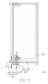
- FIG. 1shows a top view of a conventional pixel structure of a TFT array substrate.
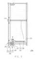
- FIG. 2is a cross-sectional view of the conventional pixel structure of the TFT array substrate, providing the cut-open view of the line I-I′ shown in FIG. 1 .
- the conventional pixel structure 100 of the TFT array substratecomprises a substrate 110 , a first metal layer 120 , a dielectric layer 130 , a semiconductor layer 140 , a second metal layer 150 , a protection layer 160 and a pixel electrode 170 .
- the first metal layer 120disposed on the substrate 110 , comprises a gate 122 and a scan line 124 electrically thereto.
- the dielectric layer 130covers the first metal layer 120 including the gate 122 .
- the second metal layer 150comprises a source/drain 152 / 154 , disposed on the semiconductor layer 140 , which partially overlaps the gate 122 , and a data line 156 , which electrically connects to the source 152 and partially overlaps the scan line 124 .
- the protection layer 160disposed on the substrate 110 , overlaps the first metal layer 120 and the second metal layer 150 .
- the protection layer 160comprises an opening 162 for exposing the drain 154 , wherein the pixel electrode 170 electrically connects to the drain 154 through the opening 162 of the protection layer 160 .
- the first metal layer 120 and the second metal layer 150are partially overlapped, so as a parasitic capacitance is produced in the overlapped location thereof.
- the parasitic capacitanceoccurs between the gate 122 and the source/drain 152 / 154 and the area between the scan line 124 and the data line 156 , so that the parasitic capacitance affects the pixel's voltage causes a signal distortion and the display quality of the LCD degrades.
- the present inventionis directed to provide a pixel structure for reducing parasitic capacitance between a first metal layer and a second metal layer, thereby further improving the display quality of an LCD.
- a pixel structurecomprises a substrate, a first metal layer, a dielectric layer, a semiconductor layer, a second metal layer, a patterned floating metal layer and a pixel electrode.
- the first metal layerdisposed on the substrate, comprises a gate and a scan line electrically thereto.
- the dielectric layercovered by the semiconductor layer and disposed on the substrate, overlaps the first metal layer.
- the second metal layercomprises a source/drain, disposed on the semiconductor layer, partially overlaps the gate, and a data line, which electrically connects to the source and partially overlaps the scan line.
- the pixel electrodeelectrically connects to the drain.
- the patterned floating metal layeris disposed between the dielectric layer and the semiconductor layer. A portion of the patterned floating metal layer, located in the, partically overlaps the gate.
- Said pixel structurefurther comprises a pad layer, disposed on the area of the dielectric layer between the scan line and the data line.
- the patterned floating metal layeris disposed between the pad layer and the dielectric layer, wherein the pad layer and the semiconductor layer are formed on the same layer.
- the first metal layerfurther comprises a common line, which is substantially parallel to the scan line and partially overlaps the data line.
- said pixel structurefurther comprises a pad layer, disposed on the area of the dielectric layer located between the scan line and the data line, and on the area of the dielectric layer between the common line and the data line.
- the patterned floating metal layeris disposed between the pad layer and the dielectric layer, wherein the pad layer and the semiconductor layer are formed on the same layer.
- the patterned floating metal layeris identical to that of the second metal layer. Additionally, the pixel structure further comprises a pad layer, disposed on the patterned floating metal layer and the data line. The pad layer and the semiconductor layer are formed on the same layer, wherein material of the patterned floating metal layer may be an opaque metal.
- material of the patterned floating metal layermay be a transparent metal.
- thickness of the patterned floating metal layermay range from 100 angstrom to 1800 angstrom.
- thickness of the patterned floating metal layermay range from 500 angstrom to 1500 angstrom.
- the semiconductor layermay comprise a channel layer and an ohmic contact layer disposed on the channel layer.
- Said structurefurther comprises a protection layer, disposed on the substrate and overlapping the first metal layer and the second layer. Additionally, the protection layer further comprises an opening for exposing the drain, wherein the pixel electrode electrically connects to the drain through the opening of the protection layer.
- parasitic capacitances connected in seriesare produced in the areas between the first metal layer and the patterned floating metal layer, and the second layer and the patterned floating metal layer by depositing the floating patterned metal layer. Accordingly, the present invention can reduce the parasitic capacitance between the first metal layer and the second layer to upgrade the display quality of the LCD.
- FIG. 1shows a top view of a conventional pixel structure of a TFT array substrate.
- FIG. 2is a cross-sectional view of the line I-I′ shown in FIG. 1 , showing the conventional pixel structure of the TFT.
- FIG. 3shows a top view of a pixel structure of a preferred embodiment of the present invention.
- FIG. 4Ashows a cross-sectional view of the line II-II′ shown in FIG. 3 .
- FIG. 4Bshows a cross-sectional view of the line III-III′ shown in FIG. 3 .
- FIG. 5shows a top view of another pixel structure of a preferred embodiment of the present invention.
- FIG. 6shows a cross-sectional view of the line IV-IV′ shown in FIG. 5 .
- FIG. 7schematically shows a top view of a pixel structure of another preferred embodiment of the present invention.
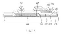
- FIG. 8shows a cross-sectional view of the line V-V′ shown in FIG. 7 .
- FIG. 3shows a top view of a pixel structure of a preferred embodiment of the present invention.
- FIG. 4Ashows a cross-sectional view of the line II-II′ shown in FIG. 3 .
- a pixel structure 200 of this embodimentcomprises a substrate 210 , a first metal layer 220 , a dielectric layer 230 , a semiconductor layer 240 , a second metal layer 250 , a patterned floating metal layer 260 and a pixel electrode 270 .
- the first metal layer 220disposed on the substrate 210 , comprises a gate 222 and a scan line 224 electrically thereto.
- the dielectric layer 230covered by the semiconductor layer 240 , is disposed on the substrate 210 and overlaps the first metal layer 220 .
- the second metal layer 250comprises a source/drain 252 / 254 , disposed on the semiconductor layer 240 and partially overlapping the gate 222 , and a data line 256 , electrically connects to the source 252 and partially overlaps the scan line 224 .
- the pixel electrode 270electrically connects to the drain 254 .
- the patterned floating metal layer 260is disposed between the dielectric layer 230 and the semiconductor layer 240 and beneath the source/drain 252 / 254 and partically overlapping the gate 222 .
- Said pixel structure 200further comprises a protection layer 280 , disposed on the substrate 210 and overlapping the first metal layer 220 and the second layer 250 . Additionally, the protection layer 280 further comprises an opening 282 for exposing the drain 254 , wherein the pixel electrode 270 electrically connects to the drain 254 through the opening 282 of the protection layer 280 . Additionally, material of the pixel electrode 270 may be Indium Tin Oxide (ITO), Indium Zinc Oxide (IZO) or other transparent conductor materials.
- the semiconductor layer 240may comprise a channel layer and an ohmic contact layer disposed on the channel layer.
- material of the patterned floating metal layer 260may be transparent metal (such as, ITO,IZO) or other opaque metal (such as, Al, Ni and Cr), thickness of which ranges from 100 angstrom to 1800 angstrom, preferably, from 500 angstrom to 1500 angstrom.
- transparent metalsuch as, ITO,IZO
- opaque metalsuch as, Al, Ni and Cr
- the parasitic capacitance between the gate 222 and the source/drain 252 / 254not only causes a signal distortion, but also affects the pixel's voltage and degrades the display quality of the LCD.
- the patterned floating metal layer 260is deposed between the gate 222 and the source 252 , and between the gate 222 and the drain 254 , so that parasitic capacitances connected in series can be formed between the gate 222 and the patterned floating metal layer 260 , and between the patterned floating metal layer 260 and the source 252 .
- parasitic capacitances connected in seriescan be formed between the gate 222 and the patterned floating metal layer 260 , and between the patterned floating metal layer 260 and the drain 254 .
- the pixel structure 200 of this embodimentcan reduce the parasitic capacitance's effect between the gate and the source/drain as well as improve the display quality of the LCD and increase the tolerance of designing the display panel.
- FIG. 4Bshows a cross-sectional view of the line III-III′ shown in FIG. 3 .
- the concept of the implementation of capacitances connected in series discussed abovecan broadly apply to the overlapped area between the first metal layer and the second metal layer, in addition to applying to the gate and the source/drain.
- the patterned floating metal layer 260is also disposed at the overlapped area between the scan line 224 and the data line 254 .
- the pixel structure 200further comprises a pad layer 245 , disposed on the dielectric layer 239 located between the scan line 224 and the data line 250 .
- the patterned floating metal layer 260is disposed between the pad layer 245 and the dielectric layer 230 . Accordingly, the parasitic capacitance between the scan line 224 and the data line 245 has less affect on a transmitted signal; therefore, the display quality of the LCD upgrades.
- the pad layer 245 and the semiconductor layer 240are formed on the same layer.
- FIG. 5shows a top view of another pixel structure of a preferred embodiment of the present invention.
- FIG. 6shows a cross-sectional of the line IV-IV′ shown in FIG. 5 .
- this pixel structure 200 ais similar to the pixel structure 200 , except for the first metal 200 of the pixel structure 200 a further comprising a common line 226 , substantially parallel to the scan line 224 and partially overlap the data line 256 .
- the pad layer 245is further disposed on the dielectric layer 230 located between the common line 226 and the data line 256 , and the patterned floating metal layer 260 is also disposed between the dielectric layer 230 and the pad layer 245 .
- FIG. 7schematically shows a top view of a pixel structure of another preferred embodiment of the present invention.
- FIG. 8shows a cross-sectional view of the line V-V′ shown in FIG. 7 .
- a mask for forming the patterned floating metal layer 260is identical to the one for forming the second metal 250 , so that the pattern of the patterned floating metal layer 260 is identical to that of the second metal 250 .
- the patterns of the patterned floating metal layer 260 and the second metal 250are identical and the semiconductor layer 240 a of this embodiment needs to extend in a way to overlap the patterned floating metal layer 260 beneath the drain 254 to prevent the patterned floating metal layer 260 from being electrically connecting to the drain 254 . Additionally, a pad layer 245 a of this embodiment needs to extend in a way to overlap the patterned floating metal layer 260 located beneath the data line 256 to prevent the patterned floating metal layer 260 from being electrically connecting to data line 256 .
- the transparent metalis selected as the material of the patterned floating metal layer 260
- area of the semiconductor layer 240 located under the drain 254is mostly and directly radiated by the light from a backlight source of the LCD without protection of the gate 222 . Accordingly, the radiated semiconductor layer 240 deteriorates and causes a photo-induced leakage current.
- opaque metalis selected as the material of the patterned floating metal layer 260 and the semiconductor layer 240 located under the drain 254 will not be deteriorated because of the protection of the patterned floating metal layer 260 . Therefore, photo-induced leakage current reduces and the display quality of the LCD upgrades.
- the pixel structure of the present inventionhas at least the following advantages:
- the present inventionutilizes the principle that total capacitance of the two capacitances connected in series is less than that of said capacitances, respectively. Therefore, the patterned floating metal layer 260 is disposed between the first metal layer and the second metal layer, so as to form the two parasitic capacitances connected in series to reduce the parasitic capacitance between the first metal layer and the second metal layer and to improve display quality and the tolerance of designing the LCD panel.
- an extra maskis not necessary due to the same mask's used to from the patterned floating metal layer and the second metal layer to lower fabricating cost because of reducing the parasitic capacitance between the first metal layer and the second metal layer.
Landscapes
- Physics & Mathematics (AREA)
- Engineering & Computer Science (AREA)
- Nonlinear Science (AREA)
- Power Engineering (AREA)
- Microelectronics & Electronic Packaging (AREA)
- Mathematical Physics (AREA)
- Chemical & Material Sciences (AREA)
- Crystallography & Structural Chemistry (AREA)
- General Physics & Mathematics (AREA)
- Optics & Photonics (AREA)
- Liquid Crystal (AREA)
- Thin Film Transistor (AREA)
Abstract
Description
Claims (11)
Priority Applications (1)
| Application Number | Priority Date | Filing Date | Title |
|---|---|---|---|
| US11/164,279US7538827B2 (en) | 2005-11-17 | 2005-11-17 | Pixel structure |
Applications Claiming Priority (1)
| Application Number | Priority Date | Filing Date | Title |
|---|---|---|---|
| US11/164,279US7538827B2 (en) | 2005-11-17 | 2005-11-17 | Pixel structure |
Publications (2)
| Publication Number | Publication Date |
|---|---|
| US20070109454A1 US20070109454A1 (en) | 2007-05-17 |
| US7538827B2true US7538827B2 (en) | 2009-05-26 |
Family
ID=38040389
Family Applications (1)
| Application Number | Title | Priority Date | Filing Date |
|---|---|---|---|
| US11/164,279Active2026-07-18US7538827B2 (en) | 2005-11-17 | 2005-11-17 | Pixel structure |
Country Status (1)
| Country | Link |
|---|---|
| US (1) | US7538827B2 (en) |
Cited By (27)
| Publication number | Priority date | Publication date | Assignee | Title |
|---|---|---|---|---|
| US20080245735A1 (en)* | 2003-10-14 | 2008-10-09 | Degussa Ag | Ceramic Flexible Membrane Providing Improved Adhesion to the Support Fleece |
| US20110157527A1 (en)* | 2009-12-29 | 2011-06-30 | Young-Jik Jo | Liquid crystal display device |
| US8552771B1 (en) | 2012-05-29 | 2013-10-08 | Life Technologies Corporation | System for reducing noise in a chemical sensor array |
| US20130271681A1 (en)* | 2012-04-12 | 2013-10-17 | Innolux Corporation | Pixel structure and liquid crystal display structure using the same |
| US8692298B2 (en) | 2006-12-14 | 2014-04-08 | Life Technologies Corporation | Chemical sensor array having multiple sensors per well |
| US8731847B2 (en) | 2010-06-30 | 2014-05-20 | Life Technologies Corporation | Array configuration and readout scheme |
| US8742472B2 (en) | 2006-12-14 | 2014-06-03 | Life Technologies Corporation | Chemically sensitive sensors with sample and hold capacitors |
| US8841217B1 (en) | 2013-03-13 | 2014-09-23 | Life Technologies Corporation | Chemical sensor with protruded sensor surface |
| US8912005B1 (en) | 2010-09-24 | 2014-12-16 | Life Technologies Corporation | Method and system for delta double sampling |
| US8912580B2 (en) | 2009-05-29 | 2014-12-16 | Life Technologies Corporation | Active chemically-sensitive sensors with in-sensor current sources |
| US8963216B2 (en) | 2013-03-13 | 2015-02-24 | Life Technologies Corporation | Chemical sensor with sidewall spacer sensor surface |
| US8962366B2 (en) | 2013-01-28 | 2015-02-24 | Life Technologies Corporation | Self-aligned well structures for low-noise chemical sensors |
| US9116117B2 (en) | 2013-03-15 | 2015-08-25 | Life Technologies Corporation | Chemical sensor with sidewall sensor surface |
| US9128044B2 (en) | 2013-03-15 | 2015-09-08 | Life Technologies Corporation | Chemical sensors with consistent sensor surface areas |
| US9194000B2 (en) | 2008-06-25 | 2015-11-24 | Life Technologies Corporation | Methods and apparatus for measuring analytes using large scale FET arrays |
| US9239313B2 (en) | 2010-06-30 | 2016-01-19 | Life Technologies Corporation | Ion-sensing charge-accumulation circuits and methods |
| US9404920B2 (en) | 2006-12-14 | 2016-08-02 | Life Technologies Corporation | Methods and apparatus for detecting molecular interactions using FET arrays |
| US9841398B2 (en) | 2013-01-08 | 2017-12-12 | Life Technologies Corporation | Methods for manufacturing well structures for low-noise chemical sensors |
| US9927393B2 (en) | 2009-05-29 | 2018-03-27 | Life Technologies Corporation | Methods and apparatus for measuring analytes |
| US9944981B2 (en) | 2008-10-22 | 2018-04-17 | Life Technologies Corporation | Methods and apparatus for measuring analytes |
| US9960253B2 (en) | 2010-07-03 | 2018-05-01 | Life Technologies Corporation | Chemically sensitive sensor with lightly doped drains |
| US9958414B2 (en) | 2010-09-15 | 2018-05-01 | Life Technologies Corporation | Apparatus for measuring analytes including chemical sensor array |
| US10422767B2 (en) | 2013-03-15 | 2019-09-24 | Life Technologies Corporation | Chemical sensor with consistent sensor surface areas |
| US10458942B2 (en) | 2013-06-10 | 2019-10-29 | Life Technologies Corporation | Chemical sensor array having multiple sensors per well |
| WO2020073567A1 (en)* | 2018-10-10 | 2020-04-16 | 惠科股份有限公司 | Array substrate, display panel having same and manufacturing method thereof |
| US10767224B2 (en) | 2014-12-18 | 2020-09-08 | Life Technologies Corporation | High data rate integrated circuit with power management |
| US11339430B2 (en) | 2007-07-10 | 2022-05-24 | Life Technologies Corporation | Methods and apparatus for measuring analytes using large scale FET arrays |
Families Citing this family (12)
| Publication number | Priority date | Publication date | Assignee | Title |
|---|---|---|---|---|
| US8673627B2 (en) | 2009-05-29 | 2014-03-18 | Life Technologies Corporation | Apparatus and methods for performing electrochemical reactions |
| US8574835B2 (en) | 2009-05-29 | 2013-11-05 | Life Technologies Corporation | Scaffolded nucleic acid polymer particles and methods of making and using |
| TWI539172B (en) | 2010-06-30 | 2016-06-21 | 生命技術公司 | Methods and apparatus for testing isfet arrays |
| US9970984B2 (en) | 2011-12-01 | 2018-05-15 | Life Technologies Corporation | Method and apparatus for identifying defects in a chemical sensor array |
| US8747748B2 (en) | 2012-01-19 | 2014-06-10 | Life Technologies Corporation | Chemical sensor with conductive cup-shaped sensor surface |
| US8821798B2 (en) | 2012-01-19 | 2014-09-02 | Life Technologies Corporation | Titanium nitride as sensing layer for microwell structure |
| CN105589242B (en)* | 2012-04-12 | 2019-07-05 | 群康科技(深圳)有限公司 | Dot structure substrate and the liquid crystal display panel for applying it |
| US9080968B2 (en) | 2013-01-04 | 2015-07-14 | Life Technologies Corporation | Methods and systems for point of use removal of sacrificial material |
| KR102593647B1 (en) | 2014-12-18 | 2023-10-26 | 라이프 테크놀로지스 코포레이션 | High data rate integrated circuit with transmitter configuration |
| CN106847829A (en)* | 2017-02-22 | 2017-06-13 | 深圳市华星光电技术有限公司 | A kind of preparation method of array base palte and array base palte |
| US11201176B2 (en) | 2017-08-08 | 2021-12-14 | Boe Technology Group Co., Ltd. | Array substrate, display apparatus, and method of fabricating array substrate |
| CN114660860B (en)* | 2022-03-21 | 2024-03-01 | 惠科股份有限公司 | Display panel and display device |
Citations (3)
| Publication number | Priority date | Publication date | Assignee | Title |
|---|---|---|---|---|
| US5151806A (en)* | 1990-04-27 | 1992-09-29 | Mitsubishi Denki Kabushiki Kaisha | Liquid crystal display apparatus having a series combination of the storage capacitors |
| US5742075A (en)* | 1994-10-07 | 1998-04-21 | Iowa State University Research Foundation, Inc. | Amorphous silicon on insulator VLSI circuit structures |
| US5747928A (en)* | 1994-10-07 | 1998-05-05 | Iowa State University Research Foundation, Inc. | Flexible panel display having thin film transistors driving polymer light-emitting diodes |
- 2005
- 2005-11-17USUS11/164,279patent/US7538827B2/enactiveActive
Patent Citations (5)
| Publication number | Priority date | Publication date | Assignee | Title |
|---|---|---|---|---|
| US5151806A (en)* | 1990-04-27 | 1992-09-29 | Mitsubishi Denki Kabushiki Kaisha | Liquid crystal display apparatus having a series combination of the storage capacitors |
| US5742075A (en)* | 1994-10-07 | 1998-04-21 | Iowa State University Research Foundation, Inc. | Amorphous silicon on insulator VLSI circuit structures |
| US5747928A (en)* | 1994-10-07 | 1998-05-05 | Iowa State University Research Foundation, Inc. | Flexible panel display having thin film transistors driving polymer light-emitting diodes |
| US5821688A (en)* | 1994-10-07 | 1998-10-13 | Iowa State University Research Foundation | Flexible panel display having thin film transistors driving polymer light-emitting diodes |
| US6017794A (en)* | 1994-10-07 | 2000-01-25 | Iowa State University Research Foundation | Method of making amorphous silicon on insulator VLSI circuit structures with floating gates |
Cited By (70)
| Publication number | Priority date | Publication date | Assignee | Title |
|---|---|---|---|---|
| US8142920B2 (en) | 2003-10-14 | 2012-03-27 | Evonik Degussa Gmbh | Ceramic, flexible membrane providing improved adhesion to the support fleece |
| US7959011B2 (en)* | 2003-10-14 | 2011-06-14 | Evonik Degussa Gmbh | Ceramic flexible membrane providing improved adhesion to the support fleece |
| US20080245735A1 (en)* | 2003-10-14 | 2008-10-09 | Degussa Ag | Ceramic Flexible Membrane Providing Improved Adhesion to the Support Fleece |
| US20110206971A1 (en)* | 2003-10-14 | 2011-08-25 | Degussa Ag | Ceramic, flexible membrane providing improved adhesion to the support fleece |
| US11435314B2 (en) | 2006-12-14 | 2022-09-06 | Life Technologies Corporation | Chemically-sensitive sensor array device |
| US8890216B2 (en) | 2006-12-14 | 2014-11-18 | Life Technologies Corporation | Methods and apparatus for measuring analytes using large scale FET arrays |
| US12066399B2 (en) | 2006-12-14 | 2024-08-20 | Life Technologies Corporation | Methods and apparatus for measuring analytes using large scale FET arrays |
| US8692298B2 (en) | 2006-12-14 | 2014-04-08 | Life Technologies Corporation | Chemical sensor array having multiple sensors per well |
| US9404920B2 (en) | 2006-12-14 | 2016-08-02 | Life Technologies Corporation | Methods and apparatus for detecting molecular interactions using FET arrays |
| US11732297B2 (en)* | 2006-12-14 | 2023-08-22 | Life Technologies Corporation | Methods and apparatus for measuring analytes using large scale FET arrays |
| US8742472B2 (en) | 2006-12-14 | 2014-06-03 | Life Technologies Corporation | Chemically sensitive sensors with sample and hold capacitors |
| US20220340965A1 (en)* | 2006-12-14 | 2022-10-27 | Life Technologies Corporation | Methods and Apparatus for Measuring Analytes Using Large Scale FET Arrays |
| US8766328B2 (en) | 2006-12-14 | 2014-07-01 | Life Technologies Corporation | Chemically-sensitive sample and hold sensors |
| US9134269B2 (en) | 2006-12-14 | 2015-09-15 | Life Technologies Corporation | Methods and apparatus for measuring analytes using large scale FET arrays |
| US9951382B2 (en) | 2006-12-14 | 2018-04-24 | Life Technologies Corporation | Methods and apparatus for measuring analytes using large scale FET arrays |
| US12140560B2 (en) | 2006-12-14 | 2024-11-12 | Life Technologies Corporation | Methods and apparatus for measuring analytes using large scale FET arrays |
| US9989489B2 (en) | 2006-12-14 | 2018-06-05 | Life Technnologies Corporation | Methods for calibrating an array of chemically-sensitive sensors |
| US10502708B2 (en) | 2006-12-14 | 2019-12-10 | Life Technologies Corporation | Chemically-sensitive sensor array calibration circuitry |
| US10816506B2 (en) | 2006-12-14 | 2020-10-27 | Life Technologies Corporation | Method for measuring analytes using large scale chemfet arrays |
| US9023189B2 (en) | 2006-12-14 | 2015-05-05 | Life Technologies Corporation | High density sensor array without wells |
| US10633699B2 (en) | 2006-12-14 | 2020-04-28 | Life Technologies Corporation | Methods and apparatus for measuring analytes using large scale FET arrays |
| US11339430B2 (en) | 2007-07-10 | 2022-05-24 | Life Technologies Corporation | Methods and apparatus for measuring analytes using large scale FET arrays |
| US9194000B2 (en) | 2008-06-25 | 2015-11-24 | Life Technologies Corporation | Methods and apparatus for measuring analytes using large scale FET arrays |
| US12146853B2 (en) | 2008-10-22 | 2024-11-19 | Life Technologies Corporation | Methods and apparatus including array of reaction chambers over array of chemFET sensors for measuring analytes |
| US11137369B2 (en) | 2008-10-22 | 2021-10-05 | Life Technologies Corporation | Integrated sensor arrays for biological and chemical analysis |
| US9944981B2 (en) | 2008-10-22 | 2018-04-17 | Life Technologies Corporation | Methods and apparatus for measuring analytes |
| US11448613B2 (en) | 2008-10-22 | 2022-09-20 | Life Technologies Corporation | ChemFET sensor array including overlying array of wells |
| US11874250B2 (en) | 2008-10-22 | 2024-01-16 | Life Technologies Corporation | Integrated sensor arrays for biological and chemical analysis |
| US10809226B2 (en) | 2009-05-29 | 2020-10-20 | Life Technologies Corporation | Methods and apparatus for measuring analytes |
| US11768171B2 (en) | 2009-05-29 | 2023-09-26 | Life Technologies Corporation | Methods and apparatus for measuring analytes |
| US10718733B2 (en) | 2009-05-29 | 2020-07-21 | Life Technologies Corporation | Methods and apparatus for measuring analytes |
| US12038405B2 (en) | 2009-05-29 | 2024-07-16 | Life Technologies Corporation | Methods and apparatus for measuring analytes |
| US8912580B2 (en) | 2009-05-29 | 2014-12-16 | Life Technologies Corporation | Active chemically-sensitive sensors with in-sensor current sources |
| US9927393B2 (en) | 2009-05-29 | 2018-03-27 | Life Technologies Corporation | Methods and apparatus for measuring analytes |
| US11692964B2 (en) | 2009-05-29 | 2023-07-04 | Life Technologies Corporation | Methods and apparatus for measuring analytes |
| US20110157527A1 (en)* | 2009-12-29 | 2011-06-30 | Young-Jik Jo | Liquid crystal display device |
| US12038406B2 (en) | 2010-06-30 | 2024-07-16 | Life Technologies Corporation | Semiconductor-based chemical detection device |
| US9239313B2 (en) | 2010-06-30 | 2016-01-19 | Life Technologies Corporation | Ion-sensing charge-accumulation circuits and methods |
| US8742471B2 (en) | 2010-06-30 | 2014-06-03 | Life Technologies Corporation | Chemical sensor array with leakage compensation circuit |
| US8731847B2 (en) | 2010-06-30 | 2014-05-20 | Life Technologies Corporation | Array configuration and readout scheme |
| US8741680B2 (en) | 2010-06-30 | 2014-06-03 | Life Technologies Corporation | Two-transistor pixel array |
| US8983783B2 (en) | 2010-06-30 | 2015-03-17 | Life Technologies Corporation | Chemical detection device having multiple flow channels |
| US10481123B2 (en) | 2010-06-30 | 2019-11-19 | Life Technologies Corporation | Ion-sensing charge-accumulation circuits and methods |
| US9960253B2 (en) | 2010-07-03 | 2018-05-01 | Life Technologies Corporation | Chemically sensitive sensor with lightly doped drains |
| US9958414B2 (en) | 2010-09-15 | 2018-05-01 | Life Technologies Corporation | Apparatus for measuring analytes including chemical sensor array |
| US12050195B2 (en) | 2010-09-15 | 2024-07-30 | Life Technologies Corporation | Methods and apparatus for measuring analytes using chemfet arrays |
| US9110015B2 (en) | 2010-09-24 | 2015-08-18 | Life Technologies Corporation | Method and system for delta double sampling |
| US8912005B1 (en) | 2010-09-24 | 2014-12-16 | Life Technologies Corporation | Method and system for delta double sampling |
| US9097949B2 (en)* | 2012-04-12 | 2015-08-04 | Innolux Corporation | Pixel structure and liquid crystal display structure using the same |
| US20130271681A1 (en)* | 2012-04-12 | 2013-10-17 | Innolux Corporation | Pixel structure and liquid crystal display structure using the same |
| US20150309378A1 (en)* | 2012-04-12 | 2015-10-29 | Innolux Corporation | Pixel structure and liquid crystal display structure using the same |
| US9703159B2 (en)* | 2012-04-12 | 2017-07-11 | Innolux Corporation | Pixel structure substrate and liquid crystal display structure using the same |
| US9270264B2 (en) | 2012-05-29 | 2016-02-23 | Life Technologies Corporation | System for reducing noise in a chemical sensor array |
| US8552771B1 (en) | 2012-05-29 | 2013-10-08 | Life Technologies Corporation | System for reducing noise in a chemical sensor array |
| US8786331B2 (en) | 2012-05-29 | 2014-07-22 | Life Technologies Corporation | System for reducing noise in a chemical sensor array |
| US9841398B2 (en) | 2013-01-08 | 2017-12-12 | Life Technologies Corporation | Methods for manufacturing well structures for low-noise chemical sensors |
| US10436742B2 (en) | 2013-01-08 | 2019-10-08 | Life Technologies Corporation | Methods for manufacturing well structures for low-noise chemical sensors |
| US8962366B2 (en) | 2013-01-28 | 2015-02-24 | Life Technologies Corporation | Self-aligned well structures for low-noise chemical sensors |
| US8963216B2 (en) | 2013-03-13 | 2015-02-24 | Life Technologies Corporation | Chemical sensor with sidewall spacer sensor surface |
| US9995708B2 (en) | 2013-03-13 | 2018-06-12 | Life Technologies Corporation | Chemical sensor with sidewall spacer sensor surface |
| US8841217B1 (en) | 2013-03-13 | 2014-09-23 | Life Technologies Corporation | Chemical sensor with protruded sensor surface |
| US10422767B2 (en) | 2013-03-15 | 2019-09-24 | Life Technologies Corporation | Chemical sensor with consistent sensor surface areas |
| US9116117B2 (en) | 2013-03-15 | 2015-08-25 | Life Technologies Corporation | Chemical sensor with sidewall sensor surface |
| US9128044B2 (en) | 2013-03-15 | 2015-09-08 | Life Technologies Corporation | Chemical sensors with consistent sensor surface areas |
| US11774401B2 (en) | 2013-06-10 | 2023-10-03 | Life Technologies Corporation | Chemical sensor array having multiple sensors per well |
| US11499938B2 (en) | 2013-06-10 | 2022-11-15 | Life Technologies Corporation | Chemical sensor array having multiple sensors per well |
| US10458942B2 (en) | 2013-06-10 | 2019-10-29 | Life Technologies Corporation | Chemical sensor array having multiple sensors per well |
| US10816504B2 (en) | 2013-06-10 | 2020-10-27 | Life Technologies Corporation | Chemical sensor array having multiple sensors per well |
| US10767224B2 (en) | 2014-12-18 | 2020-09-08 | Life Technologies Corporation | High data rate integrated circuit with power management |
| WO2020073567A1 (en)* | 2018-10-10 | 2020-04-16 | 惠科股份有限公司 | Array substrate, display panel having same and manufacturing method thereof |
Also Published As
| Publication number | Publication date |
|---|---|
| US20070109454A1 (en) | 2007-05-17 |
Similar Documents
| Publication | Publication Date | Title |
|---|---|---|
| US7538827B2 (en) | Pixel structure | |
| US9281320B2 (en) | Array substrate and liquid crystal display apparatus having the same | |
| US6819383B2 (en) | Forming method of liquid crystal layer using ink jet system | |
| KR101293950B1 (en) | Display substrate and display panel having the same | |
| US6927814B2 (en) | Array substrate for LCD and method of fabricating the same | |
| US7576824B2 (en) | Liquid crystal display device and method for fabricating the same | |
| US20050122442A1 (en) | Liquid crystal display device and method of fabricating the same | |
| US7855767B2 (en) | Transflective liquid crystal display | |
| EP2261730B1 (en) | Pixel designs of improving the aperture ratio in an LCD | |
| US8553193B2 (en) | Pixel structure and display panel having the same | |
| US8730418B2 (en) | Array substrate and method for manufacturing the same | |
| US7268839B2 (en) | Array substrate comprising an island shaped drain electrode enclosed by the source electrode and liquid crystal display device including the same | |
| CN100378516C (en) | Compensation capacitor structure of liquid crystal display | |
| US20060061700A1 (en) | Display device having a transistor electrode overlapping a capacitor electrode | |
| EP3674787B1 (en) | Liquid crystal display device | |
| US6999060B2 (en) | Liquid crystal display and fabricating method thereof | |
| US20060028603A1 (en) | Liquid crystal display device and method of fabricating the same | |
| JP2004061952A (en) | Liquid crystal display | |
| KR20090005817A (en) | Display board and display panel having same | |
| KR20040085797A (en) | Liquid crystal display and method for manufacturing the same | |
| KR20120014866A (en) | Liquid crystal display device and manufacturing method thereof | |
| KR20080000208A (en) | LCD and its manufacturing method | |
| KR20070120231A (en) | Liquid crystal display panel | |
| JP2006322978A (en) | Pixel storage capacitor structure of liquid crystal display panel | |
| KR20050046926A (en) | Thin film transistor array panel |
Legal Events
| Date | Code | Title | Description |
|---|---|---|---|
| AS | Assignment | Owner name:CHUNGHWA PICTURE TUBES, LTD., TAIWAN Free format text:ASSIGNMENT OF ASSIGNORS INTEREST;ASSIGNOR:CHOU, REY-YUAN;REEL/FRAME:016789/0921 Effective date:20051115 Owner name:CHUNGHWA PICTURE TUBES, LTD.,TAIWAN Free format text:ASSIGNMENT OF ASSIGNORS INTEREST;ASSIGNOR:CHOU, REY-YUAN;REEL/FRAME:016789/0921 Effective date:20051115 | |
| STCF | Information on status: patent grant | Free format text:PATENTED CASE | |
| FPAY | Fee payment | Year of fee payment:4 | |
| AS | Assignment | Owner name:HWZ INTANGIBLE ASSETS INVESTMENT MANAGEMENT LIMITE Free format text:ASSIGNMENT OF ASSIGNORS INTEREST;ASSIGNOR:CHUNGHWA PICTURE TUBES, LTD.;REEL/FRAME:039332/0949 Effective date:20160620 | |
| AS | Assignment | Owner name:WUHAN CHINA STAR OPTOELECTRONICS TECHNOLOGY CO., L Free format text:ASSIGNMENT OF ASSIGNORS INTEREST;ASSIGNOR:HWZ INTANGIBLE ASSETS INVESTMENT MANAGEMENT LIMITED;REEL/FRAME:040174/0599 Effective date:20161017 | |
| FEPP | Fee payment procedure | Free format text:PAYOR NUMBER ASSIGNED (ORIGINAL EVENT CODE: ASPN); ENTITY STATUS OF PATENT OWNER: LARGE ENTITY | |
| FPAY | Fee payment | Year of fee payment:8 | |
| SULP | Surcharge for late payment | Year of fee payment:7 | |
| AS | Assignment | Owner name:TCL CHINA STAR OPTOELECTRONICS TECHNOLOGY CO., LTD., CHINA Free format text:CHANGE OF NAME;ASSIGNOR:SHENZHEN CHINA STAR OPTOELECTRONICS TECHNOLOGY CO., LTD.;REEL/FRAME:052417/0828 Effective date:20191030 | |
| AS | Assignment | Owner name:FLEX DISPLAY SOLUTIONS, LLC, TEXAS Free format text:ASSIGNMENT OF ASSIGNORS INTEREST;ASSIGNOR:WUHAN CHINA STAR OPTOELECTRONICS TECHNOLOGY CO LTD;REEL/FRAME:052793/0723 Effective date:20190918 | |
| MAFP | Maintenance fee payment | Free format text:PAYMENT OF MAINTENANCE FEE, 12TH YEAR, LARGE ENTITY (ORIGINAL EVENT CODE: M1553); ENTITY STATUS OF PATENT OWNER: LARGE ENTITY Year of fee payment:12 |