US7538040B2 - Techniques for precision pattern transfer of carbon nanotubes from photo mask to wafers - Google Patents
Techniques for precision pattern transfer of carbon nanotubes from photo mask to wafersDownload PDFInfo
- Publication number
- US7538040B2 US7538040B2US11/298,274US29827405AUS7538040B2US 7538040 B2US7538040 B2US 7538040B2US 29827405 AUS29827405 AUS 29827405AUS 7538040 B2US7538040 B2US 7538040B2
- Authority
- US
- United States
- Prior art keywords
- hard mask
- etching
- layer
- mask film
- plasma
- Prior art date
- Legal status (The legal status is an assumption and is not a legal conclusion. Google has not performed a legal analysis and makes no representation as to the accuracy of the status listed.)
- Expired - Fee Related, expires
Links
Images


Classifications
- H—ELECTRICITY
- H01—ELECTRIC ELEMENTS
- H01L—SEMICONDUCTOR DEVICES NOT COVERED BY CLASS H10
- H01L21/00—Processes or apparatus adapted for the manufacture or treatment of semiconductor or solid state devices or of parts thereof
- H01L21/70—Manufacture or treatment of devices consisting of a plurality of solid state components formed in or on a common substrate or of parts thereof; Manufacture of integrated circuit devices or of parts thereof
- H01L21/71—Manufacture of specific parts of devices defined in group H01L21/70
- H01L21/768—Applying interconnections to be used for carrying current between separate components within a device comprising conductors and dielectrics
- H01L21/76838—Applying interconnections to be used for carrying current between separate components within a device comprising conductors and dielectrics characterised by the formation and the after-treatment of the conductors
- B—PERFORMING OPERATIONS; TRANSPORTING
- B82—NANOTECHNOLOGY
- B82Y—SPECIFIC USES OR APPLICATIONS OF NANOSTRUCTURES; MEASUREMENT OR ANALYSIS OF NANOSTRUCTURES; MANUFACTURE OR TREATMENT OF NANOSTRUCTURES
- B82Y10/00—Nanotechnology for information processing, storage or transmission, e.g. quantum computing or single electron logic
- H—ELECTRICITY
- H01—ELECTRIC ELEMENTS
- H01L—SEMICONDUCTOR DEVICES NOT COVERED BY CLASS H10
- H01L21/00—Processes or apparatus adapted for the manufacture or treatment of semiconductor or solid state devices or of parts thereof
- H01L21/02—Manufacture or treatment of semiconductor devices or of parts thereof
- H01L21/04—Manufacture or treatment of semiconductor devices or of parts thereof the devices having potential barriers, e.g. a PN junction, depletion layer or carrier concentration layer
- H01L21/18—Manufacture or treatment of semiconductor devices or of parts thereof the devices having potential barriers, e.g. a PN junction, depletion layer or carrier concentration layer the devices having semiconductor bodies comprising elements of Group IV of the Periodic Table or AIIIBV compounds with or without impurities, e.g. doping materials
- H01L21/30—Treatment of semiconductor bodies using processes or apparatus not provided for in groups H01L21/20 - H01L21/26
- H01L21/31—Treatment of semiconductor bodies using processes or apparatus not provided for in groups H01L21/20 - H01L21/26 to form insulating layers thereon, e.g. for masking or by using photolithographic techniques; After treatment of these layers; Selection of materials for these layers
- H01L21/3205—Deposition of non-insulating-, e.g. conductive- or resistive-, layers on insulating layers; After-treatment of these layers
- H01L21/321—After treatment
- H01L21/3213—Physical or chemical etching of the layers, e.g. to produce a patterned layer from a pre-deposited extensive layer
- H01L21/32133—Physical or chemical etching of the layers, e.g. to produce a patterned layer from a pre-deposited extensive layer by chemical means only
- H01L21/32135—Physical or chemical etching of the layers, e.g. to produce a patterned layer from a pre-deposited extensive layer by chemical means only by vapour etching only
- H01L21/32136—Physical or chemical etching of the layers, e.g. to produce a patterned layer from a pre-deposited extensive layer by chemical means only by vapour etching only using plasmas
- H—ELECTRICITY
- H01—ELECTRIC ELEMENTS
- H01L—SEMICONDUCTOR DEVICES NOT COVERED BY CLASS H10
- H01L21/00—Processes or apparatus adapted for the manufacture or treatment of semiconductor or solid state devices or of parts thereof
- H01L21/02—Manufacture or treatment of semiconductor devices or of parts thereof
- H01L21/04—Manufacture or treatment of semiconductor devices or of parts thereof the devices having potential barriers, e.g. a PN junction, depletion layer or carrier concentration layer
- H01L21/18—Manufacture or treatment of semiconductor devices or of parts thereof the devices having potential barriers, e.g. a PN junction, depletion layer or carrier concentration layer the devices having semiconductor bodies comprising elements of Group IV of the Periodic Table or AIIIBV compounds with or without impurities, e.g. doping materials
- H01L21/30—Treatment of semiconductor bodies using processes or apparatus not provided for in groups H01L21/20 - H01L21/26
- H01L21/31—Treatment of semiconductor bodies using processes or apparatus not provided for in groups H01L21/20 - H01L21/26 to form insulating layers thereon, e.g. for masking or by using photolithographic techniques; After treatment of these layers; Selection of materials for these layers
- H01L21/3205—Deposition of non-insulating-, e.g. conductive- or resistive-, layers on insulating layers; After-treatment of these layers
- H01L21/321—After treatment
- H01L21/3213—Physical or chemical etching of the layers, e.g. to produce a patterned layer from a pre-deposited extensive layer
- H01L21/32139—Physical or chemical etching of the layers, e.g. to produce a patterned layer from a pre-deposited extensive layer using masks
- H—ELECTRICITY
- H10—SEMICONDUCTOR DEVICES; ELECTRIC SOLID-STATE DEVICES NOT OTHERWISE PROVIDED FOR
- H10K—ORGANIC ELECTRIC SOLID-STATE DEVICES
- H10K71/00—Manufacture or treatment specially adapted for the organic devices covered by this subclass
- H10K71/20—Changing the shape of the active layer in the devices, e.g. patterning
- H10K71/231—Changing the shape of the active layer in the devices, e.g. patterning by etching of existing layers
- H10K71/233—Changing the shape of the active layer in the devices, e.g. patterning by etching of existing layers by photolithographic etching
- H—ELECTRICITY
- H10—SEMICONDUCTOR DEVICES; ELECTRIC SOLID-STATE DEVICES NOT OTHERWISE PROVIDED FOR
- H10K—ORGANIC ELECTRIC SOLID-STATE DEVICES
- H10K85/00—Organic materials used in the body or electrodes of devices covered by this subclass
- H10K85/20—Carbon compounds, e.g. carbon nanotubes or fullerenes
- H10K85/221—Carbon nanotubes
- Y—GENERAL TAGGING OF NEW TECHNOLOGICAL DEVELOPMENTS; GENERAL TAGGING OF CROSS-SECTIONAL TECHNOLOGIES SPANNING OVER SEVERAL SECTIONS OF THE IPC; TECHNICAL SUBJECTS COVERED BY FORMER USPC CROSS-REFERENCE ART COLLECTIONS [XRACs] AND DIGESTS
- Y10—TECHNICAL SUBJECTS COVERED BY FORMER USPC
- Y10S—TECHNICAL SUBJECTS COVERED BY FORMER USPC CROSS-REFERENCE ART COLLECTIONS [XRACs] AND DIGESTS
- Y10S977/00—Nanotechnology
- Y10S977/70—Nanostructure
- Y10S977/734—Fullerenes, i.e. graphene-based structures, such as nanohorns, nanococoons, nanoscrolls or fullerene-like structures, e.g. WS2 or MoS2 chalcogenide nanotubes, planar C3N4, etc.
- Y10S977/742—Carbon nanotubes, CNTs
Definitions
- the present inventiongenerally relates to carbon nanotubes, and more specifically relates to a technique for precisely transferring a carbon nanotube pattern from a photomask to a wafer.
- Carbon nanotube technologyis fast becoming a technological area to make an impact in electronic devices.
- Single-wall carbon nanotubesare quasi-one dimensional nanowires, which exhibit either metallic of semiconducting properties, depending upon their chirality and radius.
- Single-wall nanotubeshave been demonstrated as both semiconducting layers in thin film transistors as well as metallic interconnects between metal layers.
- FIGS. 1-3illustrate a first method which is currently used.
- a top viewis provided on the left, and a side view is provided on the right.
- a CNT layer 10is provided on a substrate 12 and a resist 14 is patterned on the CNT layer 10 .
- O 2 plasmais used to etch the CNTs 10 (i.e., from the locations identified by reference numeral 16 ).
- the resistis stripped using wet chemistry.
- Disadvantages of this methodinclude the fact that the O 2 plasma tends to lateral etch both the CNTs and resist. Where the resist lateral dimension reduces, the final CNTs pattern line width also decreases as indicated in the progression of FIG. 1 to FIG. 2 , wherein the width of both the CNTs and the resist has decreased (despite the fact that the plasma etching was intended to merely etch any CNT which was not covered by the resist). Actually, the higher the pressure of the O 2 plasma, the more dimension loss there tends to be. In addition, it is usually difficult to use wet strip chemistry to strip the organic antireflective layer (i.e., the resist). Therefore, resist patterning often remains on the (CNTs), and this may lead to high reflectance for the pattern light, and poor profile for the resist patterns. All this results in difficult control of the critical dimension of the CNT pattern.
- FIGS. 4-6illustrate a first method which is currently used.
- a top viewis provided on the left, and a side view is provided on the right.
- a CNT layer 10is provided on a substrate 12
- a hard mask layer 13is provided on the CNT layer 10
- a resist 14is patterned on the hard mask layer 13 .
- the hard mask 13 and the CNT layer 10is etched away (i.e., those portions which are not covered by the resist—identified with reference numeral 16 in FIG. 5 ).
- the resistis ashed away using O 2 plasma.
- Disadvantages of this methodinclude the fact that after the hard mask and CNT layers are etched, the O 2 plasma which is used to ash the resist attacks the CNTs from the hard mask sidewall (i.e., the plasma undercuts the hard mask and attacks the CNTs underneath). This results in a resulting, physical CNT pattern which is narrower than that of the design.
- An object of an embodiment of the present inventionis to provide an improved technique for transferring a carbon nanotube pattern to a wafer.
- Another object of an embodiment of the present inventionis to provide a method for patterning CNTs on a wafer where the CNTs do not become exposed to high O 2 plasma during patterning.
- Still another object of an embodiment of the present inventionis to provide a method for patterning CNTs on a wafer where the critical dimension of the CNTs are maintained.
- an embodiment of the present inventionprovides a method for patterning CNTs on a wafer wherein a CNT layer is provided on a substrate, a hard mask film is deposited on the CNT layer, a BARC layer (optional) is coated on the hard mask film, and a resist is patterned on the BARC layer (or directly on the hard mask film if the BARC layer is not included).
- the resist patternis effectively transferred to the hard mask film by etching the BARC layer (if provided) and etching partly into, but not entirely through, the hard mask film (i.e., etching is stopped before reaching the CNT layer) Then, the resist and the BARC layer (if provided) is stripped, such as by using O 2 plasma. Finally, the hard mask pattern is effectively transferred to the CNTs by etching away (preferably by using a Cl, F based plasma) the portions of the hard mask which have been already partially etched in a previous step.
- FIGS. 1-3are views which relate to a currently used method of patterning CNTs on a wafer
- FIGS. 4-6are views which relate to another currently used method of patterning CNTs on a wafer
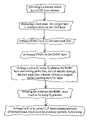
- FIGS. 7( a ) and 7 ( b )are block diagram which set forth the steps of methods of patterning CNTs on a wafer, where the methods are in accordance with embodiments of the present invention.
- FIGS. 8-11are views which relate to the method illustrated in FIG. 7( a ).
- FIG. 7( a )A method which is in accordance with an embodiment of the present invention is illustrated in FIG. 7( a ), and FIGS. 8-11 provides views which relate to the method shown in FIG. 7( a ). In each one of FIGS. 8-11 , a top view is provided on the left, and a side view is provided on the right.
- the methodprovides that initially a CNT layer 100 is provided on a substrate 102 , a hard mask film 104 (the hard mask film 104 could be binary to improve the etch control) is deposited on the CNT layer 100 , a BARC layer 106 (optional) is coated on the hard mask film 104 , and a resist 108 is patterned on the BARC layer 106 (or directly on the hard mask film if the BARC layer is not included). Then, as shown in FIGS.
- the resist patternis effectively transferred to the hard mask film 104 by etching the BARC layer 106 (if provided) (such as by using O 2 plasma or other plasma such as Cl, F) and etching partly into, but not entirely through, the hard mask film 104 (i.e., etching is stopped before reaching the CNT layer 100 ). While a binary hard mask layer will make the etch a little easier, it is not required. Then, as shown in FIGS. 7( a ) and 10 , the resist 108 and the BARC layer 106 (if provided) are stripped, such as by using O 2 plasma. Finally, as shown in FIGS.
- the hard mask patternis effectively transferred to the CNTs by etching away (preferably by using a highly directional plasma, such as a Cl, F based plasma) the portions of the hard mask 104 which have been already partially etched in a previous step (i.e., from the areas identified with reference numeral 110 ).
- a highly directional plasmasuch as a Cl, F based plasma
- the hard maskeither a dual layer hard mask can be used wherein only a top layer of the hard mask is initially etched away, or a single layer hard mask can be used but where the etching stops before the CNTs are reached.
- FIG. 7( b )illustrates effectively the same method but where the BARC layer is not included.
- Advantages of the present inventioninclude the fact that the CNTs are not exposed to O 2 plasma during patterning, a BARC layer can be used for the photomask step, and the critical dimension is maintained from the resist pattern to the CNT patterns.
- the present inventioncan be applied to any application which needs pattern CNTs.
Landscapes
- Engineering & Computer Science (AREA)
- Physics & Mathematics (AREA)
- Manufacturing & Machinery (AREA)
- Microelectronics & Electronic Packaging (AREA)
- Chemical & Material Sciences (AREA)
- Power Engineering (AREA)
- Condensed Matter Physics & Semiconductors (AREA)
- General Physics & Mathematics (AREA)
- Computer Hardware Design (AREA)
- Nanotechnology (AREA)
- Chemical Kinetics & Catalysis (AREA)
- General Chemical & Material Sciences (AREA)
- Mathematical Physics (AREA)
- Theoretical Computer Science (AREA)
- Crystallography & Structural Chemistry (AREA)
- Plasma & Fusion (AREA)
- Carbon And Carbon Compounds (AREA)
- Drying Of Semiconductors (AREA)
Abstract
Description
Claims (15)
Priority Applications (2)
| Application Number | Priority Date | Filing Date | Title |
|---|---|---|---|
| US11/298,274US7538040B2 (en) | 2005-06-30 | 2005-12-08 | Techniques for precision pattern transfer of carbon nanotubes from photo mask to wafers |
| US12/471,175US7911034B2 (en) | 2005-06-30 | 2009-05-22 | Techniques for precision pattern transfer of carbon nanotubes from photo mask to wafers |
Applications Claiming Priority (2)
| Application Number | Priority Date | Filing Date | Title |
|---|---|---|---|
| US69633605P | 2005-06-30 | 2005-06-30 | |
| US11/298,274US7538040B2 (en) | 2005-06-30 | 2005-12-08 | Techniques for precision pattern transfer of carbon nanotubes from photo mask to wafers |
Related Child Applications (1)
| Application Number | Title | Priority Date | Filing Date |
|---|---|---|---|
| US12/471,175ContinuationUS7911034B2 (en) | 2005-06-30 | 2009-05-22 | Techniques for precision pattern transfer of carbon nanotubes from photo mask to wafers |
Publications (2)
| Publication Number | Publication Date |
|---|---|
| US20070004191A1 US20070004191A1 (en) | 2007-01-04 |
| US7538040B2true US7538040B2 (en) | 2009-05-26 |
Family
ID=37590159
Family Applications (2)
| Application Number | Title | Priority Date | Filing Date |
|---|---|---|---|
| US11/298,274Expired - Fee RelatedUS7538040B2 (en) | 2005-06-30 | 2005-12-08 | Techniques for precision pattern transfer of carbon nanotubes from photo mask to wafers |
| US12/471,175Expired - Fee RelatedUS7911034B2 (en) | 2005-06-30 | 2009-05-22 | Techniques for precision pattern transfer of carbon nanotubes from photo mask to wafers |
Family Applications After (1)
| Application Number | Title | Priority Date | Filing Date |
|---|---|---|---|
| US12/471,175Expired - Fee RelatedUS7911034B2 (en) | 2005-06-30 | 2009-05-22 | Techniques for precision pattern transfer of carbon nanotubes from photo mask to wafers |
Country Status (1)
| Country | Link |
|---|---|
| US (2) | US7538040B2 (en) |
Cited By (2)
| Publication number | Priority date | Publication date | Assignee | Title |
|---|---|---|---|---|
| US20090183816A1 (en)* | 2008-01-17 | 2009-07-23 | Samsung Electronics Co., Ltd. | Method of transferring carbon nanotubes |
| US20090294754A1 (en)* | 2005-06-30 | 2009-12-03 | Nantero, Inc. | Novel techniques for precision pattern transfer of carbon nanotubes from photo mask to wafers |
Families Citing this family (89)
| Publication number | Priority date | Publication date | Assignee | Title |
|---|---|---|---|---|
| US7563711B1 (en)* | 2001-07-25 | 2009-07-21 | Nantero, Inc. | Method of forming a carbon nanotube-based contact to semiconductor |
| US7566478B2 (en)* | 2001-07-25 | 2009-07-28 | Nantero, Inc. | Methods of making carbon nanotube films, layers, fabrics, ribbons, elements and articles |
| US7259410B2 (en)* | 2001-07-25 | 2007-08-21 | Nantero, Inc. | Devices having horizontally-disposed nanofabric articles and methods of making the same |
| US6835591B2 (en)* | 2001-07-25 | 2004-12-28 | Nantero, Inc. | Methods of nanotube films and articles |
| US6706402B2 (en) | 2001-07-25 | 2004-03-16 | Nantero, Inc. | Nanotube films and articles |
| US6919592B2 (en)* | 2001-07-25 | 2005-07-19 | Nantero, Inc. | Electromechanical memory array using nanotube ribbons and method for making same |
| US9574290B2 (en) | 2003-01-13 | 2017-02-21 | Nantero Inc. | Methods for arranging nanotube elements within nanotube fabrics and films |
| US7858185B2 (en)* | 2003-09-08 | 2010-12-28 | Nantero, Inc. | High purity nanotube fabrics and films |
| US8937575B2 (en) | 2009-07-31 | 2015-01-20 | Nantero Inc. | Microstrip antenna elements and arrays comprising a shaped nanotube fabric layer and integrated two terminal nanotube select devices |
| EP1585845A1 (en)* | 2003-01-13 | 2005-10-19 | Nantero, Inc. | Methods of using thin metal layers to make carbon nanotube films, layers, fabrics, ribbons, elements and articles |
| US7560136B2 (en)* | 2003-01-13 | 2009-07-14 | Nantero, Inc. | Methods of using thin metal layers to make carbon nanotube films, layers, fabrics, ribbons, elements and articles |
| CA2526946A1 (en)* | 2003-05-14 | 2005-04-07 | Nantero, Inc. | Sensor platform using a non-horizontally oriented nanotube element |
| US7416993B2 (en) | 2003-09-08 | 2008-08-26 | Nantero, Inc. | Patterned nanowire articles on a substrate and methods of making the same |
| US7375369B2 (en)* | 2003-09-08 | 2008-05-20 | Nantero, Inc. | Spin-coatable liquid for formation of high purity nanotube films |
| US7709880B2 (en)* | 2004-06-09 | 2010-05-04 | Nantero, Inc. | Field effect devices having a gate controlled via a nanotube switching element |
| TWI399864B (en)* | 2004-09-16 | 2013-06-21 | Nantero Inc | Light emitters using nanotubes and methods of making same |
| WO2006132658A2 (en)* | 2004-09-21 | 2006-12-14 | Nantero, Inc. | Resistive elements using carbon nanotubes |
| CA2586120A1 (en)* | 2004-11-02 | 2006-12-28 | Nantero, Inc. | Nanotube esd protective devices and corresponding nonvolatile and volatile nanotube switches |
| US20100147657A1 (en)* | 2004-11-02 | 2010-06-17 | Nantero, Inc. | Nanotube esd protective devices and corresponding nonvolatile and volatile nanotube switches |
| EP1825038B1 (en)* | 2004-12-16 | 2012-09-12 | Nantero, Inc. | Aqueous carbon nanotube applicator liquids and methods for producing applicator liquids thereof |
| US8941094B2 (en) | 2010-09-02 | 2015-01-27 | Nantero Inc. | Methods for adjusting the conductivity range of a nanotube fabric layer |
| US9287356B2 (en)* | 2005-05-09 | 2016-03-15 | Nantero Inc. | Nonvolatile nanotube diodes and nonvolatile nanotube blocks and systems using same and methods of making same |
| US7835170B2 (en) | 2005-05-09 | 2010-11-16 | Nantero, Inc. | Memory elements and cross point switches and arrays of same using nonvolatile nanotube blocks |
| US9196615B2 (en)* | 2005-05-09 | 2015-11-24 | Nantero Inc. | Nonvolatile nanotube diodes and nonvolatile nanotube blocks and systems using same and methods of making same |
| US7782650B2 (en)* | 2005-05-09 | 2010-08-24 | Nantero, Inc. | Nonvolatile nanotube diodes and nonvolatile nanotube blocks and systems using same and methods of making same |
| US8217490B2 (en)* | 2005-05-09 | 2012-07-10 | Nantero Inc. | Nonvolatile nanotube diodes and nonvolatile nanotube blocks and systems using same and methods of making same |
| US9911743B2 (en) | 2005-05-09 | 2018-03-06 | Nantero, Inc. | Nonvolatile nanotube diodes and nonvolatile nanotube blocks and systems using same and methods of making same |
| US8013363B2 (en)* | 2005-05-09 | 2011-09-06 | Nantero, Inc. | Nonvolatile nanotube diodes and nonvolatile nanotube blocks and systems using same and methods of making same |
| US8513768B2 (en)* | 2005-05-09 | 2013-08-20 | Nantero Inc. | Nonvolatile nanotube diodes and nonvolatile nanotube blocks and systems using same and methods of making same |
| US8183665B2 (en)* | 2005-11-15 | 2012-05-22 | Nantero Inc. | Nonvolatile nanotube diodes and nonvolatile nanotube blocks and systems using same and methods of making same |
| US7781862B2 (en)* | 2005-05-09 | 2010-08-24 | Nantero, Inc. | Two-terminal nanotube devices and systems and methods of making same |
| US7479654B2 (en)* | 2005-05-09 | 2009-01-20 | Nantero, Inc. | Memory arrays using nanotube articles with reprogrammable resistance |
| US7598127B2 (en) | 2005-05-12 | 2009-10-06 | Nantero, Inc. | Nanotube fuse structure |
| TWI264271B (en)* | 2005-05-13 | 2006-10-11 | Delta Electronics Inc | Heat sink |
| US7915122B2 (en)* | 2005-06-08 | 2011-03-29 | Nantero, Inc. | Self-aligned cell integration scheme |
| US7439731B2 (en) | 2005-06-24 | 2008-10-21 | Crafts Douglas E | Temporary planar electrical contact device and method using vertically-compressible nanotube contact structures |
| US8525143B2 (en)* | 2005-09-06 | 2013-09-03 | Nantero Inc. | Method and system of using nanotube fabrics as joule heating elements for memories and other applications |
| ATE518131T1 (en)* | 2005-09-06 | 2011-08-15 | Nantero Inc | NANOTUBE-BASED SENSOR SYSTEM AND METHOD FOR USE THEREOF |
| AU2006347609A1 (en) | 2005-09-06 | 2008-05-08 | Nantero, Inc. | Carbon nanotubes for the selective transfer of heat from electronics |
| JP2009528238A (en)* | 2005-12-19 | 2009-08-06 | ナンテロ,インク. | Formation of carbon nanotubes |
| US7786465B2 (en)* | 2005-12-20 | 2010-08-31 | Invention Science Fund 1, Llc | Deletable nanotube circuit |
| US9159417B2 (en)* | 2005-12-20 | 2015-10-13 | The Invention Science Fund I, Llc | Deletable nanotube circuit |
| US7989797B2 (en)* | 2005-12-20 | 2011-08-02 | The Invention Science Fund I, Llc | Connectible nanotube circuit |
| US8354855B2 (en)* | 2006-10-16 | 2013-01-15 | Formfactor, Inc. | Carbon nanotube columns and methods of making and using carbon nanotube columns as probes |
| US8130007B2 (en) | 2006-10-16 | 2012-03-06 | Formfactor, Inc. | Probe card assembly with carbon nanotube probes having a spring mechanism therein |
| WO2008127780A2 (en)* | 2007-02-21 | 2008-10-23 | Nantero, Inc. | Symmetric touch screen system with carbon nanotube-based transparent conductive electrode pairs |
| WO2008112764A1 (en) | 2007-03-12 | 2008-09-18 | Nantero, Inc. | Electromagnetic and thermal sensors using carbon nanotubes and methods of making same |
| US8115187B2 (en)* | 2007-05-22 | 2012-02-14 | Nantero, Inc. | Triodes using nanofabric articles and methods of making the same |
| US8149007B2 (en)* | 2007-10-13 | 2012-04-03 | Formfactor, Inc. | Carbon nanotube spring contact structures with mechanical and electrical components |
| EP2062515B1 (en)* | 2007-11-20 | 2012-08-29 | So, Kwok Kuen | Bowl and basket assembly and salad spinner incorporating such an assembly |
| CN102067292B (en)* | 2008-04-11 | 2013-08-14 | 桑迪士克3D有限责任公司 | Methods for etching carbon nano-tube films for use in non-volatile memories |
| CN101582449B (en)* | 2008-05-14 | 2011-12-14 | 清华大学 | Thin film transistor |
| CN101599495B (en)* | 2008-06-04 | 2013-01-09 | 清华大学 | Thin-film transistor panel |
| CN101582445B (en)* | 2008-05-14 | 2012-05-16 | 清华大学 | Thin film transistor |
| CN101593699B (en)* | 2008-05-30 | 2010-11-10 | 清华大学 | Method for preparing thin film transistor |
| CN101582448B (en)* | 2008-05-14 | 2012-09-19 | 清华大学 | thin film transistor |
| CN101582447B (en) | 2008-05-14 | 2010-09-29 | 清华大学 | thin film transistor |
| CN101587839B (en) | 2008-05-23 | 2011-12-21 | 清华大学 | Method for producing thin film transistors |
| CN101582446B (en) | 2008-05-14 | 2011-02-02 | 鸿富锦精密工业(深圳)有限公司 | Thin film transistor |
| CN101582444A (en) | 2008-05-14 | 2009-11-18 | 清华大学 | Thin film transistor |
| CN101582450B (en)* | 2008-05-16 | 2012-03-28 | 清华大学 | thin film transistor |
| CN101582382B (en)* | 2008-05-14 | 2011-03-23 | 鸿富锦精密工业(深圳)有限公司 | Preparation method of thin film transistor |
| CN101582451A (en)* | 2008-05-16 | 2009-11-18 | 清华大学 | Thin film transistor |
| WO2009155359A1 (en)* | 2008-06-20 | 2009-12-23 | Nantero, Inc. | Nram arrays with nanotube blocks, nanotube traces, and nanotube planes and methods of making same |
| US20100032640A1 (en)* | 2008-08-07 | 2010-02-11 | Sandisk 3D Llc | Memory cell that includes a carbon-based memory element and methods of forming the same |
| US7915637B2 (en) | 2008-11-19 | 2011-03-29 | Nantero, Inc. | Switching materials comprising mixed nanoscopic particles and carbon nanotubes and method of making and using the same |
| US8272124B2 (en)* | 2009-04-03 | 2012-09-25 | Formfactor, Inc. | Anchoring carbon nanotube columns |
| US20100252317A1 (en)* | 2009-04-03 | 2010-10-07 | Formfactor, Inc. | Carbon nanotube contact structures for use with semiconductor dies and other electronic devices |
| US8574673B2 (en) | 2009-07-31 | 2013-11-05 | Nantero Inc. | Anisotropic nanotube fabric layers and films and methods of forming same |
| US8128993B2 (en)* | 2009-07-31 | 2012-03-06 | Nantero Inc. | Anisotropic nanotube fabric layers and films and methods of forming same |
| US20110034008A1 (en)* | 2009-08-07 | 2011-02-10 | Nantero, Inc. | Method for forming a textured surface on a semiconductor substrate using a nanofabric layer |
| US20110073563A1 (en)* | 2009-09-25 | 2011-03-31 | Industrial Technology Research Institute | Patterning Method for Carbon-Based Substrate |
| US8551806B2 (en)* | 2009-10-23 | 2013-10-08 | Nantero Inc. | Methods for passivating a carbonic nanolayer |
| US8895950B2 (en) | 2009-10-23 | 2014-11-25 | Nantero Inc. | Methods for passivating a carbonic nanolayer |
| US8351239B2 (en)* | 2009-10-23 | 2013-01-08 | Nantero Inc. | Dynamic sense current supply circuit and associated method for reading and characterizing a resistive memory array |
| US8222704B2 (en)* | 2009-12-31 | 2012-07-17 | Nantero, Inc. | Compact electrical switching devices with nanotube elements, and methods of making same |
| US9617151B2 (en) | 2010-02-12 | 2017-04-11 | Nantero Inc. | Methods for controlling density, porosity, and/or gap size within nanotube fabric layers and films |
| US20110203632A1 (en)* | 2010-02-22 | 2011-08-25 | Rahul Sen | Photovoltaic devices using semiconducting nanotube layers |
| US8518472B2 (en)* | 2010-03-04 | 2013-08-27 | Guardian Industries Corp. | Large-area transparent conductive coatings including doped carbon nanotubes and nanowire composites, and methods of making the same |
| US8604332B2 (en) | 2010-03-04 | 2013-12-10 | Guardian Industries Corp. | Electronic devices including transparent conductive coatings including carbon nanotubes and nanowire composites, and methods of making the same |
| EP2552826A4 (en) | 2010-03-30 | 2013-11-13 | Nantero Inc | Methods for arranging nanoscopic elements within networks, fabrics, and films |
| US10661304B2 (en) | 2010-03-30 | 2020-05-26 | Nantero, Inc. | Microfluidic control surfaces using ordered nanotube fabrics |
| US8872176B2 (en) | 2010-10-06 | 2014-10-28 | Formfactor, Inc. | Elastic encapsulated carbon nanotube based electrical contacts |
| US9650732B2 (en) | 2013-05-01 | 2017-05-16 | Nantero Inc. | Low defect nanotube application solutions and fabrics and methods for making same |
| US10654718B2 (en) | 2013-09-20 | 2020-05-19 | Nantero, Inc. | Scalable nanotube fabrics and methods for making same |
| US9299430B1 (en) | 2015-01-22 | 2016-03-29 | Nantero Inc. | Methods for reading and programming 1-R resistive change element arrays |
| KR102515377B1 (en) | 2015-12-24 | 2023-03-28 | 삼성전자주식회사 | Composition for hard mask layer and carbon nanotube layer structure and method of forming patterns and method of manufacturing semiconductor device |
| US9934848B2 (en) | 2016-06-07 | 2018-04-03 | Nantero, Inc. | Methods for determining the resistive states of resistive change elements |
| US9941001B2 (en) | 2016-06-07 | 2018-04-10 | Nantero, Inc. | Circuits for determining the resistive states of resistive change elements |
Citations (110)
| Publication number | Priority date | Publication date | Assignee | Title |
|---|---|---|---|---|
| US4979149A (en) | 1986-09-10 | 1990-12-18 | Lgz Landis & Gyr Zug Ag | Non-volatile memory device including a micro-mechanical storage element |
| WO1998039250A1 (en) | 1997-03-07 | 1998-09-11 | William Marsh Rice University | Carbon fibers formed from single-wall carbon nanotubes |
| WO1999065821A1 (en) | 1998-06-19 | 1999-12-23 | The Research Foundation Of State University Of New York | Free-standing and aligned carbon nanotubes and synthesis thereof |
| US6057637A (en) | 1996-09-13 | 2000-05-02 | The Regents Of The University Of California | Field emission electron source |
| JP2000203821A (en) | 1999-01-18 | 2000-07-25 | Toshiyuki Tsuboi | Method for forming film of carbon nanotube, carbon nanotube film formed by the method and electric field electron release source using the same |
| US6100109A (en) | 1994-11-02 | 2000-08-08 | Siemens Aktiengesellschaft | Method for producing a memory device |
| US6128214A (en) | 1999-03-29 | 2000-10-03 | Hewlett-Packard | Molecular wire crossbar memory |
| WO2001003208A1 (en) | 1999-07-02 | 2001-01-11 | President And Fellows Of Harvard College | Nanoscopic wire-based devices, arrays, and methods of their manufacture |
| US6250984B1 (en) | 1999-01-25 | 2001-06-26 | Agere Systems Guardian Corp. | Article comprising enhanced nanotube emitter structure and process for fabricating article |
| US20010004979A1 (en) | 1999-12-14 | 2001-06-28 | Lg Electronics Inc. | Field emission display and method for fabricating the same |
| US6256767B1 (en) | 1999-03-29 | 2001-07-03 | Hewlett-Packard Company | Demultiplexer for a molecular wire crossbar network (MWCN DEMUX) |
| US6277318B1 (en) | 1999-08-18 | 2001-08-21 | Agere Systems Guardian Corp. | Method for fabrication of patterned carbon nanotube films |
| WO2000048195A9 (en) | 1999-02-12 | 2001-11-01 | Univ Michigan State | Nanocapsules containing charged particles, their uses and methods of forming the same |
| US6314019B1 (en) | 1999-03-29 | 2001-11-06 | Hewlett-Packard Company | Molecular-wire crossbar interconnect (MWCI) for signal routing and communications |
| US6342276B1 (en) | 1999-12-10 | 2002-01-29 | Samsung Sdi Co., Ltd. | Method for making a field emission display |
| GB2364933A (en) | 2000-07-18 | 2002-02-13 | Lg Electronics Inc | Method of horizontally growing carbon nanotubes and field effect transistor using the carbon nanotubes grown by the method |
| WO2002048701A2 (en) | 2000-12-11 | 2002-06-20 | President And Fellows Of Harvard College | Nanosensors |
| US6409567B1 (en) | 1997-12-15 | 2002-06-25 | E.I. Du Pont De Nemours And Company | Past-deposited carbon electron emitters |
| US6423583B1 (en) | 2001-01-03 | 2002-07-23 | International Business Machines Corporation | Methodology for electrically induced selective breakdown of nanotubes |
| US6426687B1 (en) | 2001-05-22 | 2002-07-30 | The Aerospace Corporation | RF MEMS switch |
| US6445006B1 (en) | 1995-12-20 | 2002-09-03 | Advanced Technology Materials, Inc. | Microelectronic and microelectromechanical devices comprising carbon nanotube components, and methods of making same |
| US6443901B1 (en) | 2000-06-15 | 2002-09-03 | Koninklijke Philips Electronics N.V. | Capacitive micromachined ultrasonic transducers |
| US20020160111A1 (en) | 2001-04-25 | 2002-10-31 | Yi Sun | Method for fabrication of field emission devices using carbon nanotube film as a cathode |
| US6495116B1 (en) | 2000-04-10 | 2002-12-17 | Lockheed Martin Corporation | Net shape manufacturing using carbon nanotubes |
| US6495258B1 (en) | 2000-09-20 | 2002-12-17 | Auburn University | Structures with high number density of carbon nanotubes and 3-dimensional distribution |
| US20030004058A1 (en) | 2001-05-21 | 2003-01-02 | Trustees Of Boston College | Varied morphology carbon nanotubes and method for their manufacture |
| WO2003016901A1 (en) | 2001-08-14 | 2003-02-27 | Samsung Electronics Co., Ltd. | Sensor for detecting biomolecule using carbon nanotubes |
| US6528020B1 (en) | 1998-08-14 | 2003-03-04 | The Board Of Trustees Of The Leland Stanford Junior University | Carbon nanotube devices |
| US6548841B2 (en) | 2000-11-09 | 2003-04-15 | Texas Instruments Incorporated | Nanomechanical switches and circuits |
| WO2003034142A1 (en) | 2001-10-18 | 2003-04-24 | National Institute Of Advanced Industrial Science And Technology | Optical element, and manufacturing method thereof |
| US20030122111A1 (en) | 2001-03-26 | 2003-07-03 | Glatkowski Paul J. | Coatings comprising carbon nanotubes and methods for forming same |
| US20030177450A1 (en) | 2002-03-12 | 2003-09-18 | Alex Nugent | Physical neural network design incorporating nanotechnology |
| US6630772B1 (en) | 1998-09-21 | 2003-10-07 | Agere Systems Inc. | Device comprising carbon nanotube field emitter structure and process for forming device |
| US20030200521A1 (en) | 2002-01-18 | 2003-10-23 | California Institute Of Technology | Array-based architecture for molecular electronics |
| US6645628B2 (en) | 2001-11-13 | 2003-11-11 | The United States Of America As Represented By The Secretary Of The Air Force | Carbon nanotube coated anode |
| US20040005723A1 (en) | 2002-04-02 | 2004-01-08 | Nanosys, Inc. | Methods of making, positioning and orienting nanostructures, nanostructure arrays and nanostructure devices |
| US20040007528A1 (en) | 2002-07-03 | 2004-01-15 | The Regents Of The University Of California | Intertwined, free-standing carbon nanotube mesh for use as separation, concentration, and/or filtration medium |
| US20040023253A1 (en) | 2001-06-11 | 2004-02-05 | Sandeep Kunwar | Device structure for closely spaced electrodes |
| US20040043527A1 (en) | 2002-09-04 | 2004-03-04 | Nanomix, Inc. | Sensitivity control for nanotube sensors |
| US20040041154A1 (en) | 2002-09-04 | 2004-03-04 | Fuji Xerox Co., Ltd. | Electric part and method of manufacturing the same |
| US20040043219A1 (en)* | 2000-11-29 | 2004-03-04 | Fuminori Ito | Pattern forming method for carbon nanotube, and field emission cold cathode and method of manufacturing the cold cathode |
| US6707098B2 (en) | 2000-07-04 | 2004-03-16 | Infineon Technologies, Ag | Electronic device and method for fabricating an electronic device |
| US20040071949A1 (en) | 2001-07-27 | 2004-04-15 | Glatkowski Paul J. | Conformal coatings comprising carbon nanotubes |
| US20040099438A1 (en) | 2002-05-21 | 2004-05-27 | Arthur David J. | Method for patterning carbon nanotube coating and carbon nanotube wiring |
| US20040104129A1 (en) | 2002-11-27 | 2004-06-03 | Gang Gu | Nanotube chemical sensor based on work function of electrodes |
| US6803840B2 (en) | 2001-03-30 | 2004-10-12 | California Institute Of Technology | Pattern-aligned carbon nanotube growth and tunable resonator apparatus |
| US6808746B1 (en) | 1999-04-16 | 2004-10-26 | Commonwealth Scientific and Industrial Research Organisation Campell | Multilayer carbon nanotube films and method of making the same |
| US6809462B2 (en) | 2000-04-05 | 2004-10-26 | Sri International | Electroactive polymer sensors |
| US20040238907A1 (en) | 2003-06-02 | 2004-12-02 | Pinkerton Joseph F. | Nanoelectromechanical transistors and switch systems |
| US20040253167A1 (en) | 2001-07-27 | 2004-12-16 | Silva Sembukutiarachilage Ravi | Production of carbon nanotubes |
| US6833558B2 (en) | 2000-08-23 | 2004-12-21 | Korea Institute Of Science And Technology | Parallel and selective growth method of carbon nanotube on the substrates for electronic-spintronic device applications |
| US20040265550A1 (en) | 2002-12-06 | 2004-12-30 | Glatkowski Paul J. | Optically transparent nanostructured electrical conductors |
| US6858197B1 (en) | 2002-03-13 | 2005-02-22 | The United States Of America As Represented By The Administrator Of The National Aeronautics And Space Administration | Controlled patterning and growth of single wall and multi-wall carbon nanotubes |
| US20050047244A1 (en) | 2003-03-28 | 2005-03-03 | Nantero, Inc. | Four terminal non-volatile transistor device |
| US20050053525A1 (en) | 2003-05-14 | 2005-03-10 | Nantero, Inc. | Sensor platform using a horizontally oriented nanotube element |
| US20050052894A1 (en) | 2003-09-09 | 2005-03-10 | Nantero, Inc. | Uses of nanofabric-based electro-mechanical switches |
| US20050058834A1 (en) | 2001-07-25 | 2005-03-17 | Nantero, Inc. | Nanotube films and articles |
| US20050058797A1 (en) | 2003-09-08 | 2005-03-17 | Nantero, Inc. | High purity nanotube fabrics and films |
| US20050056825A1 (en) | 2003-06-09 | 2005-03-17 | Nantero, Inc. | Field effect devices having a drain controlled via a nanotube switching element |
| US20050059210A1 (en) | 2003-04-22 | 2005-03-17 | Nantero, Inc. | Process for making bit selectable devices having elements made with nanotubes |
| US20050058590A1 (en) | 2003-09-08 | 2005-03-17 | Nantero, Inc. | Spin-coatable liquid for formation of high purity nanotube films |
| US20050059176A1 (en) | 2003-04-22 | 2005-03-17 | Nantero, Inc. | Process for making byte erasable devices having elements made with nanotubes |
| US20050056877A1 (en) | 2003-03-28 | 2005-03-17 | Nantero, Inc. | Nanotube-on-gate fet structures and applications |
| US20050063210A1 (en) | 2001-07-25 | 2005-03-24 | Nantero, Inc. | Hybrid circuit having nanotube electromechanical memory |
| US20050068128A1 (en) | 2003-06-20 | 2005-03-31 | David Yip | Anchorless electrostatically activated micro electromechanical system switch |
| US20050095938A1 (en) | 2003-10-29 | 2005-05-05 | Rosenberger Brian T. | Carbon nanotube fabrics |
| US20050101112A1 (en) | 2001-07-25 | 2005-05-12 | Nantero, Inc. | Methods of nanotubes films and articles |
| US6899945B2 (en) | 2002-03-19 | 2005-05-31 | William Marsh Rice University | Entangled single-wall carbon nanotube solid material and methods for making same |
| US20050128788A1 (en) | 2003-09-08 | 2005-06-16 | Nantero, Inc. | Patterned nanoscopic articles and methods of making the same |
| US6918284B2 (en) | 2003-03-24 | 2005-07-19 | The United States Of America As Represented By The Secretary Of The Navy | Interconnected networks of single-walled carbon nanotubes |
| US6919740B2 (en) | 2003-01-31 | 2005-07-19 | Hewlett-Packard Development Company, Lp. | Molecular-junction-nanowire-crossbar-based inverter, latch, and flip-flop circuits, and more complex circuits composed, in part, from molecular-junction-nanowire-crossbar-based inverter, latch, and flip-flop circuits |
| US6919592B2 (en) | 2001-07-25 | 2005-07-19 | Nantero, Inc. | Electromechanical memory array using nanotube ribbons and method for making same |
| US6921575B2 (en) | 2001-05-21 | 2005-07-26 | Fuji Xerox Co., Ltd. | Carbon nanotube structures, carbon nanotube devices using the same and method for manufacturing carbon nanotube structures |
| US6924538B2 (en) | 2001-07-25 | 2005-08-02 | Nantero, Inc. | Devices having vertically-disposed nanofabric articles and methods of making the same |
| US20050174842A1 (en) | 2004-02-11 | 2005-08-11 | Nantero, Inc. | EEPROMS using carbon nanotubes for cell storage |
| US20050184294A1 (en)* | 2004-01-21 | 2005-08-25 | Yuegang Zhang | End functionalization of carbon nanotubes |
| US6946410B2 (en) | 2002-04-05 | 2005-09-20 | E. I. Du Pont De Nemours And Company | Method for providing nano-structures of uniform length |
| US20050214195A1 (en)* | 2004-03-27 | 2005-09-29 | Jung Hee T | Method for manufacturing a carbon nanotube multilayer pattern using photolithography and dry etching |
| US6955937B1 (en) | 2004-08-12 | 2005-10-18 | Lsi Logic Corporation | Carbon nanotube memory cell for integrated circuit structure with removable side spacers to permit access to memory cell and process for forming such memory cell |
| US20050237781A1 (en) | 2003-06-09 | 2005-10-27 | Nantero, Inc. | Non-volatile electromechanical field effect devices and circuits using same and methods of forming same |
| US6969651B1 (en) | 2004-03-26 | 2005-11-29 | Lsi Logic Corporation | Layout design and process to form nanotube cell for nanotube memory applications |
| US20050266605A1 (en)* | 2004-06-01 | 2005-12-01 | Canon Kabushiki Kaisha | Process for patterning nanocarbon material, semiconductor device, and method for manufacturing semiconductor device |
| US20050272342A1 (en)* | 2004-06-04 | 2005-12-08 | Teco Nanotech Co., Ltd. | Patterned carbon nanotube process |
| US20050269553A1 (en) | 2003-09-08 | 2005-12-08 | Nantero, Inc. | Spin-coatable liquid for use in electronic fabrication processes |
| US20050269554A1 (en) | 2004-06-03 | 2005-12-08 | Nantero, Inc. | Applicator liquid containing ethyl lactate for preparation of nanotube films |
| US20050282516A1 (en) | 2004-06-18 | 2005-12-22 | Nantero, Inc. | Receiver circuit using nanotube-based switches and logic |
| US6990009B2 (en) | 2003-08-13 | 2006-01-24 | Nantero, Inc. | Nanotube-based switching elements with multiple controls |
| US20060044035A1 (en) | 2004-06-18 | 2006-03-02 | Nantero, Inc. | Storage elements using nanotube switching elements |
| US20060061389A1 (en) | 2004-06-18 | 2006-03-23 | Nantero, Inc. | Integrated nanotube and field effect switching device |
| US7057402B2 (en) | 2002-03-18 | 2006-06-06 | Honeywell International Inc. | Carbon nanotube sensor |
| US20060183278A1 (en) | 2005-01-14 | 2006-08-17 | Nantero, Inc. | Field effect device having a channel of nanofabric and methods of making same |
| US20060193093A1 (en) | 2004-11-02 | 2006-08-31 | Nantero, Inc. | Nanotube ESD protective devices and corresponding nonvolatile and volatile nanotube switches |
| US20060204427A1 (en) | 2004-12-16 | 2006-09-14 | Nantero, Inc. | Aqueous carbon nanotube applicator liquids and methods for producing applicator liquids thereof |
| US20060231865A1 (en) | 2001-12-28 | 2006-10-19 | Nantero, Inc. | Electromechanical three-trace junction devices |
| US20060237799A1 (en) | 2005-04-21 | 2006-10-26 | Lsi Logic Corporation | Carbon nanotube memory cells having flat bottom electrode contact surface |
| US20060250843A1 (en) | 2005-05-09 | 2006-11-09 | Nantero, Inc. | Non-volatile-shadow latch using a nanotube switch |
| US20060250856A1 (en) | 2005-05-09 | 2006-11-09 | Nantero, Inc. | Memory arrays using nanotube articles with reprogrammable resistance |
| US20060255834A1 (en) | 2004-06-18 | 2006-11-16 | Nantero, Inc. | Tri-state circuit using nanotube switching elements |
| US20060276056A1 (en) | 2005-04-05 | 2006-12-07 | Nantero, Inc. | Nanotube articles with adjustable electrical conductivity and methods of making the same |
| US20060278902A1 (en) | 2005-06-10 | 2006-12-14 | Sey-Shing Sun | Nano structure electrode design |
| US20070004191A1 (en) | 2005-06-30 | 2007-01-04 | Lsi Logic Corporation | Novel techniques for precision pattern transfer of carbon nanotubes from photo mask to wafers |
| US7160169B2 (en)* | 2003-11-24 | 2007-01-09 | Samsung Sdi Co., Ltd. | Method of forming carbon nanotube emitters and field emission display (FED) including such emitters |
| US7161285B2 (en)* | 2000-11-20 | 2007-01-09 | Nec Corporation | CNT film and field-emission cold cathode comprising the same |
| US20070030721A1 (en) | 2001-07-25 | 2007-02-08 | Nantero, Inc. | Device selection circuitry constructed with nanotube technology |
| US20070063740A1 (en) | 2003-08-13 | 2007-03-22 | Nantero, Inc. | Nanotube-based switching elements and logic circuits |
| US7217374B2 (en)* | 2003-08-22 | 2007-05-15 | Fuji Xerox Co., Ltd. | Resistance element, method of manufacturing the same, and thermistor |
| US20070248758A1 (en)* | 2002-04-23 | 2007-10-25 | Ward Jonathan W | Methods of using pre-formed nanotubes to make carbon nanotube films, layers, fabrics, elements and articles |
| US7329931B2 (en) | 2004-06-18 | 2008-02-12 | Nantero, Inc. | Receiver circuit using nanotube-based switches and transistors |
| US20080231413A1 (en) | 2004-09-21 | 2008-09-25 | Nantero, Inc. | Resistive elements using carbon nanotubes |
| US20080251723A1 (en) | 2007-03-12 | 2008-10-16 | Ward Jonathan W | Electromagnetic and Thermal Sensors Using Carbon Nanotubes and Methods of Making Same |
Family Cites Families (2)
| Publication number | Priority date | Publication date | Assignee | Title |
|---|---|---|---|---|
| US7259410B2 (en) | 2001-07-25 | 2007-08-21 | Nantero, Inc. | Devices having horizontally-disposed nanofabric articles and methods of making the same |
| US20060292297A1 (en)* | 2004-07-06 | 2006-12-28 | Nano-Proprietary, Inc. | Patterning CNT emitters |
- 2005
- 2005-12-08USUS11/298,274patent/US7538040B2/ennot_activeExpired - Fee Related
- 2009
- 2009-05-22USUS12/471,175patent/US7911034B2/ennot_activeExpired - Fee Related
Patent Citations (132)
| Publication number | Priority date | Publication date | Assignee | Title |
|---|---|---|---|---|
| US4979149A (en) | 1986-09-10 | 1990-12-18 | Lgz Landis & Gyr Zug Ag | Non-volatile memory device including a micro-mechanical storage element |
| US6100109A (en) | 1994-11-02 | 2000-08-08 | Siemens Aktiengesellschaft | Method for producing a memory device |
| US6445006B1 (en) | 1995-12-20 | 2002-09-03 | Advanced Technology Materials, Inc. | Microelectronic and microelectromechanical devices comprising carbon nanotube components, and methods of making same |
| US6057637A (en) | 1996-09-13 | 2000-05-02 | The Regents Of The University Of California | Field emission electron source |
| WO1998039250A1 (en) | 1997-03-07 | 1998-09-11 | William Marsh Rice University | Carbon fibers formed from single-wall carbon nanotubes |
| US6409567B1 (en) | 1997-12-15 | 2002-06-25 | E.I. Du Pont De Nemours And Company | Past-deposited carbon electron emitters |
| US6863942B2 (en) | 1998-06-19 | 2005-03-08 | The Research Foundation Of State University Of New York | Free-standing and aligned carbon nanotubes and synthesis thereof |
| WO1999065821A1 (en) | 1998-06-19 | 1999-12-23 | The Research Foundation Of State University Of New York | Free-standing and aligned carbon nanotubes and synthesis thereof |
| US6528020B1 (en) | 1998-08-14 | 2003-03-04 | The Board Of Trustees Of The Leland Stanford Junior University | Carbon nanotube devices |
| US6630772B1 (en) | 1998-09-21 | 2003-10-07 | Agere Systems Inc. | Device comprising carbon nanotube field emitter structure and process for forming device |
| JP2000203821A (en) | 1999-01-18 | 2000-07-25 | Toshiyuki Tsuboi | Method for forming film of carbon nanotube, carbon nanotube film formed by the method and electric field electron release source using the same |
| US6250984B1 (en) | 1999-01-25 | 2001-06-26 | Agere Systems Guardian Corp. | Article comprising enhanced nanotube emitter structure and process for fabricating article |
| WO2000048195A9 (en) | 1999-02-12 | 2001-11-01 | Univ Michigan State | Nanocapsules containing charged particles, their uses and methods of forming the same |
| US6256767B1 (en) | 1999-03-29 | 2001-07-03 | Hewlett-Packard Company | Demultiplexer for a molecular wire crossbar network (MWCN DEMUX) |
| US6314019B1 (en) | 1999-03-29 | 2001-11-06 | Hewlett-Packard Company | Molecular-wire crossbar interconnect (MWCI) for signal routing and communications |
| US6128214A (en) | 1999-03-29 | 2000-10-03 | Hewlett-Packard | Molecular wire crossbar memory |
| US6808746B1 (en) | 1999-04-16 | 2004-10-26 | Commonwealth Scientific and Industrial Research Organisation Campell | Multilayer carbon nanotube films and method of making the same |
| WO2001003208A1 (en) | 1999-07-02 | 2001-01-11 | President And Fellows Of Harvard College | Nanoscopic wire-based devices, arrays, and methods of their manufacture |
| US6277318B1 (en) | 1999-08-18 | 2001-08-21 | Agere Systems Guardian Corp. | Method for fabrication of patterned carbon nanotube films |
| US6342276B1 (en) | 1999-12-10 | 2002-01-29 | Samsung Sdi Co., Ltd. | Method for making a field emission display |
| US20010004979A1 (en) | 1999-12-14 | 2001-06-28 | Lg Electronics Inc. | Field emission display and method for fabricating the same |
| US6809462B2 (en) | 2000-04-05 | 2004-10-26 | Sri International | Electroactive polymer sensors |
| US6495116B1 (en) | 2000-04-10 | 2002-12-17 | Lockheed Martin Corporation | Net shape manufacturing using carbon nanotubes |
| US6443901B1 (en) | 2000-06-15 | 2002-09-03 | Koninklijke Philips Electronics N.V. | Capacitive micromachined ultrasonic transducers |
| US6707098B2 (en) | 2000-07-04 | 2004-03-16 | Infineon Technologies, Ag | Electronic device and method for fabricating an electronic device |
| GB2364933B (en) | 2000-07-18 | 2002-12-31 | Lg Electronics Inc | Method of horizontally growing carbon nanotubes |
| US6515339B2 (en) | 2000-07-18 | 2003-02-04 | Lg Electronics Inc. | Method of horizontally growing carbon nanotubes and field effect transistor using the carbon nanotubes grown by the method |
| GB2364933A (en) | 2000-07-18 | 2002-02-13 | Lg Electronics Inc | Method of horizontally growing carbon nanotubes and field effect transistor using the carbon nanotubes grown by the method |
| US6833558B2 (en) | 2000-08-23 | 2004-12-21 | Korea Institute Of Science And Technology | Parallel and selective growth method of carbon nanotube on the substrates for electronic-spintronic device applications |
| US6495258B1 (en) | 2000-09-20 | 2002-12-17 | Auburn University | Structures with high number density of carbon nanotubes and 3-dimensional distribution |
| US6548841B2 (en) | 2000-11-09 | 2003-04-15 | Texas Instruments Incorporated | Nanomechanical switches and circuits |
| US7161285B2 (en)* | 2000-11-20 | 2007-01-09 | Nec Corporation | CNT film and field-emission cold cathode comprising the same |
| US20040043219A1 (en)* | 2000-11-29 | 2004-03-04 | Fuminori Ito | Pattern forming method for carbon nanotube, and field emission cold cathode and method of manufacturing the cold cathode |
| WO2002048701A2 (en) | 2000-12-11 | 2002-06-20 | President And Fellows Of Harvard College | Nanosensors |
| US6423583B1 (en) | 2001-01-03 | 2002-07-23 | International Business Machines Corporation | Methodology for electrically induced selective breakdown of nanotubes |
| US20030122111A1 (en) | 2001-03-26 | 2003-07-03 | Glatkowski Paul J. | Coatings comprising carbon nanotubes and methods for forming same |
| US6803840B2 (en) | 2001-03-30 | 2004-10-12 | California Institute Of Technology | Pattern-aligned carbon nanotube growth and tunable resonator apparatus |
| US20020160111A1 (en) | 2001-04-25 | 2002-10-31 | Yi Sun | Method for fabrication of field emission devices using carbon nanotube film as a cathode |
| US6921575B2 (en) | 2001-05-21 | 2005-07-26 | Fuji Xerox Co., Ltd. | Carbon nanotube structures, carbon nanotube devices using the same and method for manufacturing carbon nanotube structures |
| US20030004058A1 (en) | 2001-05-21 | 2003-01-02 | Trustees Of Boston College | Varied morphology carbon nanotubes and method for their manufacture |
| US6426687B1 (en) | 2001-05-22 | 2002-07-30 | The Aerospace Corporation | RF MEMS switch |
| US20040023253A1 (en) | 2001-06-11 | 2004-02-05 | Sandeep Kunwar | Device structure for closely spaced electrodes |
| US20070030721A1 (en) | 2001-07-25 | 2007-02-08 | Nantero, Inc. | Device selection circuitry constructed with nanotube technology |
| US6924538B2 (en) | 2001-07-25 | 2005-08-02 | Nantero, Inc. | Devices having vertically-disposed nanofabric articles and methods of making the same |
| US20050058834A1 (en) | 2001-07-25 | 2005-03-17 | Nantero, Inc. | Nanotube films and articles |
| US20070018260A1 (en) | 2001-07-25 | 2007-01-25 | Nantero, Inc. | Devices having vertically-disposed nanofabric articles and methods of making the same |
| US6919592B2 (en) | 2001-07-25 | 2005-07-19 | Nantero, Inc. | Electromechanical memory array using nanotube ribbons and method for making same |
| US20050191495A1 (en) | 2001-07-25 | 2005-09-01 | Nantero, Inc. | Nanotube films and articles |
| US20050101112A1 (en) | 2001-07-25 | 2005-05-12 | Nantero, Inc. | Methods of nanotubes films and articles |
| US20050063210A1 (en) | 2001-07-25 | 2005-03-24 | Nantero, Inc. | Hybrid circuit having nanotube electromechanical memory |
| US20060128049A1 (en) | 2001-07-25 | 2006-06-15 | Nantero, Inc. | Devices having vertically-disposed nanofabric articles and methods of making the same |
| US20040253167A1 (en) | 2001-07-27 | 2004-12-16 | Silva Sembukutiarachilage Ravi | Production of carbon nanotubes |
| US20040071949A1 (en) | 2001-07-27 | 2004-04-15 | Glatkowski Paul J. | Conformal coatings comprising carbon nanotubes |
| WO2003016901A1 (en) | 2001-08-14 | 2003-02-27 | Samsung Electronics Co., Ltd. | Sensor for detecting biomolecule using carbon nanotubes |
| WO2003034142A1 (en) | 2001-10-18 | 2003-04-24 | National Institute Of Advanced Industrial Science And Technology | Optical element, and manufacturing method thereof |
| US6645628B2 (en) | 2001-11-13 | 2003-11-11 | The United States Of America As Represented By The Secretary Of The Air Force | Carbon nanotube coated anode |
| US20060231865A1 (en) | 2001-12-28 | 2006-10-19 | Nantero, Inc. | Electromechanical three-trace junction devices |
| US20030200521A1 (en) | 2002-01-18 | 2003-10-23 | California Institute Of Technology | Array-based architecture for molecular electronics |
| US20030177450A1 (en) | 2002-03-12 | 2003-09-18 | Alex Nugent | Physical neural network design incorporating nanotechnology |
| US6858197B1 (en) | 2002-03-13 | 2005-02-22 | The United States Of America As Represented By The Administrator Of The National Aeronautics And Space Administration | Controlled patterning and growth of single wall and multi-wall carbon nanotubes |
| US7057402B2 (en) | 2002-03-18 | 2006-06-06 | Honeywell International Inc. | Carbon nanotube sensor |
| US6899945B2 (en) | 2002-03-19 | 2005-05-31 | William Marsh Rice University | Entangled single-wall carbon nanotube solid material and methods for making same |
| US20040005723A1 (en) | 2002-04-02 | 2004-01-08 | Nanosys, Inc. | Methods of making, positioning and orienting nanostructures, nanostructure arrays and nanostructure devices |
| US6946410B2 (en) | 2002-04-05 | 2005-09-20 | E. I. Du Pont De Nemours And Company | Method for providing nano-structures of uniform length |
| US20070248758A1 (en)* | 2002-04-23 | 2007-10-25 | Ward Jonathan W | Methods of using pre-formed nanotubes to make carbon nanotube films, layers, fabrics, elements and articles |
| US20040099438A1 (en) | 2002-05-21 | 2004-05-27 | Arthur David J. | Method for patterning carbon nanotube coating and carbon nanotube wiring |
| US20040007528A1 (en) | 2002-07-03 | 2004-01-15 | The Regents Of The University Of California | Intertwined, free-standing carbon nanotube mesh for use as separation, concentration, and/or filtration medium |
| US20040041154A1 (en) | 2002-09-04 | 2004-03-04 | Fuji Xerox Co., Ltd. | Electric part and method of manufacturing the same |
| US20040043527A1 (en) | 2002-09-04 | 2004-03-04 | Nanomix, Inc. | Sensitivity control for nanotube sensors |
| US20040104129A1 (en) | 2002-11-27 | 2004-06-03 | Gang Gu | Nanotube chemical sensor based on work function of electrodes |
| US20040265550A1 (en) | 2002-12-06 | 2004-12-30 | Glatkowski Paul J. | Optically transparent nanostructured electrical conductors |
| US6919740B2 (en) | 2003-01-31 | 2005-07-19 | Hewlett-Packard Development Company, Lp. | Molecular-junction-nanowire-crossbar-based inverter, latch, and flip-flop circuits, and more complex circuits composed, in part, from molecular-junction-nanowire-crossbar-based inverter, latch, and flip-flop circuits |
| US6918284B2 (en) | 2003-03-24 | 2005-07-19 | The United States Of America As Represented By The Secretary Of The Navy | Interconnected networks of single-walled carbon nanotubes |
| US20050056877A1 (en) | 2003-03-28 | 2005-03-17 | Nantero, Inc. | Nanotube-on-gate fet structures and applications |
| US20050047244A1 (en) | 2003-03-28 | 2005-03-03 | Nantero, Inc. | Four terminal non-volatile transistor device |
| US6995046B2 (en) | 2003-04-22 | 2006-02-07 | Nantero, Inc. | Process for making byte erasable devices having elements made with nanotubes |
| US20050059176A1 (en) | 2003-04-22 | 2005-03-17 | Nantero, Inc. | Process for making byte erasable devices having elements made with nanotubes |
| US20050059210A1 (en) | 2003-04-22 | 2005-03-17 | Nantero, Inc. | Process for making bit selectable devices having elements made with nanotubes |
| US20050065741A1 (en) | 2003-05-14 | 2005-03-24 | Nantero, Inc. | Sensor platform using a non-horizontally oriented nanotube element |
| US20060125033A1 (en) | 2003-05-14 | 2006-06-15 | Nantero, Inc. | Sensor platform using a non-horizontally oriented nanotube element |
| US20060237805A1 (en) | 2003-05-14 | 2006-10-26 | Nantero, Inc. | Sensor platform using a horizontally oriented nanotube element |
| US20050053525A1 (en) | 2003-05-14 | 2005-03-10 | Nantero, Inc. | Sensor platform using a horizontally oriented nanotube element |
| US20040238907A1 (en) | 2003-06-02 | 2004-12-02 | Pinkerton Joseph F. | Nanoelectromechanical transistors and switch systems |
| US20050056866A1 (en) | 2003-06-09 | 2005-03-17 | Nantero, Inc. | Circuit arrays having cells with combinations of transistors and nanotube switching elements |
| US20070108482A1 (en) | 2003-06-09 | 2007-05-17 | Nantero, Inc. | Non-volatile electromechanical field effect devices and circuits using same and methods of forming same |
| US20070020859A1 (en) | 2003-06-09 | 2007-01-25 | Nantero, Inc. | Method of making non-volatile field effect devices and arrays of same |
| US20050056825A1 (en) | 2003-06-09 | 2005-03-17 | Nantero, Inc. | Field effect devices having a drain controlled via a nanotube switching element |
| US20050062070A1 (en) | 2003-06-09 | 2005-03-24 | Nantero, Inc. | Field effect devices having a source controlled via a nanotube switching element |
| US20050062035A1 (en) | 2003-06-09 | 2005-03-24 | Nantero, Inc. | Non-volatile electromechanical field effect devices and circuits using same and methods of forming same |
| US20050062062A1 (en) | 2003-06-09 | 2005-03-24 | Nantero, Inc. | One-time programmable, non-volatile field effect devices and methods of making same |
| US20050237781A1 (en) | 2003-06-09 | 2005-10-27 | Nantero, Inc. | Non-volatile electromechanical field effect devices and circuits using same and methods of forming same |
| US20050063244A1 (en) | 2003-06-09 | 2005-03-24 | Nantero, Inc. | Field effect devices having a gate controlled via a nanotube switching element |
| US20050074926A1 (en) | 2003-06-09 | 2005-04-07 | Nantero, Inc. | Method of making non-volatile field effect devices and arrays of same |
| US20050068128A1 (en) | 2003-06-20 | 2005-03-31 | David Yip | Anchorless electrostatically activated micro electromechanical system switch |
| US20080186756A1 (en) | 2003-08-13 | 2008-08-07 | Bertin Claude L | Nanotube-Based Switching Elements with Multiple Controls |
| US20070063740A1 (en) | 2003-08-13 | 2007-03-22 | Nantero, Inc. | Nanotube-based switching elements and logic circuits |
| US6990009B2 (en) | 2003-08-13 | 2006-01-24 | Nantero, Inc. | Nanotube-based switching elements with multiple controls |
| US7339401B2 (en) | 2003-08-13 | 2008-03-04 | Nantero, Inc. | Nanotube-based switching elements with multiple controls |
| US7217374B2 (en)* | 2003-08-22 | 2007-05-15 | Fuji Xerox Co., Ltd. | Resistance element, method of manufacturing the same, and thermistor |
| US7416993B2 (en) | 2003-09-08 | 2008-08-26 | Nantero, Inc. | Patterned nanowire articles on a substrate and methods of making the same |
| US20050058590A1 (en) | 2003-09-08 | 2005-03-17 | Nantero, Inc. | Spin-coatable liquid for formation of high purity nanotube films |
| US20050269553A1 (en) | 2003-09-08 | 2005-12-08 | Nantero, Inc. | Spin-coatable liquid for use in electronic fabrication processes |
| US20050058797A1 (en) | 2003-09-08 | 2005-03-17 | Nantero, Inc. | High purity nanotube fabrics and films |
| US20050128788A1 (en) | 2003-09-08 | 2005-06-16 | Nantero, Inc. | Patterned nanoscopic articles and methods of making the same |
| US20050052894A1 (en) | 2003-09-09 | 2005-03-10 | Nantero, Inc. | Uses of nanofabric-based electro-mechanical switches |
| US20050095938A1 (en) | 2003-10-29 | 2005-05-05 | Rosenberger Brian T. | Carbon nanotube fabrics |
| US7160169B2 (en)* | 2003-11-24 | 2007-01-09 | Samsung Sdi Co., Ltd. | Method of forming carbon nanotube emitters and field emission display (FED) including such emitters |
| US20050184294A1 (en)* | 2004-01-21 | 2005-08-25 | Yuegang Zhang | End functionalization of carbon nanotubes |
| US20050174842A1 (en) | 2004-02-11 | 2005-08-11 | Nantero, Inc. | EEPROMS using carbon nanotubes for cell storage |
| US6969651B1 (en) | 2004-03-26 | 2005-11-29 | Lsi Logic Corporation | Layout design and process to form nanotube cell for nanotube memory applications |
| US20050214195A1 (en)* | 2004-03-27 | 2005-09-29 | Jung Hee T | Method for manufacturing a carbon nanotube multilayer pattern using photolithography and dry etching |
| US20050266605A1 (en)* | 2004-06-01 | 2005-12-01 | Canon Kabushiki Kaisha | Process for patterning nanocarbon material, semiconductor device, and method for manufacturing semiconductor device |
| US20050269554A1 (en) | 2004-06-03 | 2005-12-08 | Nantero, Inc. | Applicator liquid containing ethyl lactate for preparation of nanotube films |
| US20050272342A1 (en)* | 2004-06-04 | 2005-12-08 | Teco Nanotech Co., Ltd. | Patterned carbon nanotube process |
| US20050282516A1 (en) | 2004-06-18 | 2005-12-22 | Nantero, Inc. | Receiver circuit using nanotube-based switches and logic |
| US7329931B2 (en) | 2004-06-18 | 2008-02-12 | Nantero, Inc. | Receiver circuit using nanotube-based switches and transistors |
| US20060255834A1 (en) | 2004-06-18 | 2006-11-16 | Nantero, Inc. | Tri-state circuit using nanotube switching elements |
| US20080191742A1 (en) | 2004-06-18 | 2008-08-14 | Bertin Claude L | Receiver circuit using nanotube-based switches and transistors |
| US20060044035A1 (en) | 2004-06-18 | 2006-03-02 | Nantero, Inc. | Storage elements using nanotube switching elements |
| US20060061389A1 (en) | 2004-06-18 | 2006-03-23 | Nantero, Inc. | Integrated nanotube and field effect switching device |
| US6955937B1 (en) | 2004-08-12 | 2005-10-18 | Lsi Logic Corporation | Carbon nanotube memory cell for integrated circuit structure with removable side spacers to permit access to memory cell and process for forming such memory cell |
| US20080231413A1 (en) | 2004-09-21 | 2008-09-25 | Nantero, Inc. | Resistive elements using carbon nanotubes |
| US20060193093A1 (en) | 2004-11-02 | 2006-08-31 | Nantero, Inc. | Nanotube ESD protective devices and corresponding nonvolatile and volatile nanotube switches |
| US20060204427A1 (en) | 2004-12-16 | 2006-09-14 | Nantero, Inc. | Aqueous carbon nanotube applicator liquids and methods for producing applicator liquids thereof |
| US20060183278A1 (en) | 2005-01-14 | 2006-08-17 | Nantero, Inc. | Field effect device having a channel of nanofabric and methods of making same |
| US20060276056A1 (en) | 2005-04-05 | 2006-12-07 | Nantero, Inc. | Nanotube articles with adjustable electrical conductivity and methods of making the same |
| US20060237799A1 (en) | 2005-04-21 | 2006-10-26 | Lsi Logic Corporation | Carbon nanotube memory cells having flat bottom electrode contact surface |
| US20060250843A1 (en) | 2005-05-09 | 2006-11-09 | Nantero, Inc. | Non-volatile-shadow latch using a nanotube switch |
| US20060250856A1 (en) | 2005-05-09 | 2006-11-09 | Nantero, Inc. | Memory arrays using nanotube articles with reprogrammable resistance |
| US20060278902A1 (en) | 2005-06-10 | 2006-12-14 | Sey-Shing Sun | Nano structure electrode design |
| US20070004191A1 (en) | 2005-06-30 | 2007-01-04 | Lsi Logic Corporation | Novel techniques for precision pattern transfer of carbon nanotubes from photo mask to wafers |
| US20080251723A1 (en) | 2007-03-12 | 2008-10-16 | Ward Jonathan W | Electromagnetic and Thermal Sensors Using Carbon Nanotubes and Methods of Making Same |
Non-Patent Citations (42)
| Title |
|---|
| Ago et al., "Work Function of PUrified and Oxidised Carbon Nanotubes," Synthetic Metals, vol. 103, pp. 2494-2495 (1999). |
| Ajayan, P. M. et al., "Applications of Carbon Nanotubes", Carbon Nanotubes, vol. 80, pp. 391-425, 2001. |
| Avouris, P., et al., "Carbon Nanotube Electronics," Chemical Physics, 2002, vol. 284, pp. 429-445. |
| Banerjee et al., "Functionalization of Carbon Nanotubes with a Metal-Containing Molecular Complex," Nano Letters, vol. 2, No. 1, pp. 49-53 (2002). |
| Berhan, L. et al., "Mechanical properties of nanotube sheets: Alterations in joint morphology and achievable moduli in manufacturable materials", Journal of Applied Physics, vol. 95, No. 8, pp. 4335-4345, Apr. 15, 2004. |
| Bonard, J. M. et al., "Monodisperse Multiwall Carbon Nanotubes Obtained with Ferritin as Catalyst", Nano Letters, vol. 2, No. 6, pp. 665-667, 2002. |
| Bradley, K. et al., "Flexible Nanotube Electronics," Nano Letters, vol. 3, No. 10, pp. 1353-1355, 2003. |
| Cassell, A. M. et al., "Large Scale CVD Synthesis of Single-Walled Carbon Nanotubes", J. Phys. Chem. B, pp. 6484-6492, 1999. |
| Chen, B. et al., "Heterogeneous Single-Walled Carbon Nanotbue Catalyst Discovery and Optimization", Chem. Mater., vol. 14, pp. 1891-1896, 2002. |
| Cheng, H M., "Large-scale and low-cost synthesis of single-walled carbon nanotubes by the catalytic pyrolysis of hydrocarbons", Applied Physics Letters, vol. 72, No. 25, pp. 3282-3284, Jun. 22, 1998. |
| Chiang, et al., Purification and Characterization of Single-Wall Carbon Nanotubes (SWNTs) Obtained from the Gas-Phase Decomposition of CO (HiPco Process), J. Phys. Chem. B, vol. 105, pp. 8297-8301, 2001. |
| Dai, H. et al., "Controlled Chemical Routes to Nanotube Artchitectures, Physics, and Devices", J. Phys. Chem. B, vol. 103, pp. 1126-11255, 1999. |
| Delzeit et al., "Mulilayered Metal Catalysts for Controlling the Density of Single-Walled Carbon Nanotubes Growth," Chemical Physics Letters, vol. 348, pp. 368-374, Nov. 16, 2001. |
| Dequesnes, M. et al., "Calculation of pull-in voltages for carbon-nanotube-based nanoelectromechanical switches," Nanotechnology, Jan. 22, 2002, vol. 13, pp. 383-386. |
| Desai et al., "Freestanding Carbon Nanotube Specific Fabrication", Proc of 2005, 5th IEEE Conf., Nanotech, Nagoya, Japan, pp. 1-4, Jul. 2005. |
| Franklin, N. R. et al., "An Enhance CVD Approach to Extensive Nanotube Networks with Directionality", Advanced Materials, 5 pages, 2000. |
| Haddon et al., "Purification and Separation of Carbon Nanotubes," MRS Bulletin, pp. 252-259, Apr. 2004. |
| Hafner, J. H. et al., "Catalytic growth of single-wall carbon nanotubes from metal particles", Chemical Physics Letters, vol. 296, pp. 195-202, Oct. 30, 1998. |
| Homma, Y. et al., "Single Walled Carbon Nanotube Growth on Silicon Substrates Using Nanoparticle Catalysts", Jpn. J. Appl. Phys., vol., 41, Pt. 2, No. 1A/B, pp. L89-91, 2002. |
| International Search Report and Written Opinion for International Patent Application No. PCT/US05/18467, Oct. 1, 2007. |
| International Search Report for PCT/U2005/045316, Sep. 6, 2006, 2 pages. |
| International Search Report, International Patent Application No. PCT/US05/18539, Sep. 18, 2006, 4 pages. |
| Jeong et al., "A New Purification Method of Single-Wall Carbon Nanotubes Using H2S and O2 Mixutre Gas," chemical Physics Letters, vol. 344, pp. 18-22, Aug. 17, 2001. |
| Joselevich, E., "Vectorial Growth of Metallic and Semiconducting Single-Wall Carbon Nanotubes", Nano Letters, vol. 0, No. 0, A-E, 2002. |
| Kaneto et al., "Electrical conductivites of multi-wall carbon nano tubes", Synthethic Materials, Elsevier Science, SA., vol. 203, pp. 2543-2546, 1999. |
| Kong, J. et al., "Chemical vapor deposition of methane for single-walled carbon nanotubes", Chemical Physics Letters, pp. 567-574, Aug. 14, 1998. |
| Kong, J. et al., "Nanotube Molecular Wires as Chemical Sensors," Science, 2000, vol. 287 pp. 622-625. |
| Li, J. et al., "Cabon Nanotube Nanoelectrode Array for Ultrasensitive DNA Detection", Nano Letters, vol. 3, No. 5, pp. 597-602, 2003. |
| Li, Y. et al., "Growth of Single-Walled Carbon Nanotubes from Discrete Catalytic Nanoparticles of Various Sizes", J. Phys. Chem. B, vol. 105, pp. 11424-11431, 2001. |
| Li, Y. et al., "Preparation of Monodispersed Fe-Mo Nanoparticles as the Catalyst for CVD Synthesis of Carbon Nanotubes", Chem. Mater., vol. 13, pp. 1008-1014, 2001. |
| Nerushev, O.A., et al., "Carbon nanotube films obtained by thermal chemical vapour deposition", J. Mater. Chem. vol. 11, pp. 1122-1132, 2001. |
| Onoa, G.B. et al., "Bulk production of singly dispersed carbon nanotube with prescribed lengths," Nanotechnology, vol. 16, pp. 2799-2803, 2005. |
| Parikh, K. et al., "Flexible vapour sensors using single walled carbon nanotubes", Sensors and Actuators B, vol. 113, pp. 55-63, 2006. |
| Peigney, M. et al., "A Study of the Formation of Single- and Double- Walled Carbon Nanotubes by a CVD Method", J. Phys. Chem. B., vol. 105, pp. 9699-9710, 2001. |
| Qi, P. et al., "Toward Large Arrays of Multiplex Functionalization Carbon Nanotube Sensors for Highly Sensitive and Selective Molecular Detection," Nano Lett. 2003, vol. 3(3), pp. 347-351. |
| Sotiropoulou, S. et al., "Carbon nanotube array-based biosensor", Anal. Bioanal. Chem, vol. 375, pp. 103-105, 2003. |
| Stadermann, M. et al., "Nanoscale study of conduction through carbon nanotube networks," Phys. Rev. B 69, 201402(R), 2004. |
| Valentini, L. et al., "Sensors for Sub-ppm NO2Gas Detection Based on Carbon Nanotube Thin Films," Applied Physics Letters, 2003, vol. 82(6), pp. 961-963. |
| Zhang et al., "Formation of metal nanowires on suspened signel-walled carbon nanotubes", Appl. Phys. Lett., vol. 77, p. 3015, Nov. 2000. |
| Zhang, Y. et al., "Metal coating on suspended carbon Nanotubes and its implication to metal-tube interaction", Chemical Physics Letters, vol. 331, pp. 35-41, 2000. |
| Zhang, Z. et al., "Select Pathways to Carbon Nanotube Film Growth", Advanced Materials, 4 pages, Jun. 19, 2001. |
| Zhao, Y. P. et al., Frequency-dependent electrical transport in carbor nanotubes', Physical Review B., vol. 64, pp. 201402-1 to 201402-4, 2001. |
Cited By (4)
| Publication number | Priority date | Publication date | Assignee | Title |
|---|---|---|---|---|
| US20090294754A1 (en)* | 2005-06-30 | 2009-12-03 | Nantero, Inc. | Novel techniques for precision pattern transfer of carbon nanotubes from photo mask to wafers |
| US7911034B2 (en)* | 2005-06-30 | 2011-03-22 | Nantero, Inc. | Techniques for precision pattern transfer of carbon nanotubes from photo mask to wafers |
| US20090183816A1 (en)* | 2008-01-17 | 2009-07-23 | Samsung Electronics Co., Ltd. | Method of transferring carbon nanotubes |
| US8007617B2 (en)* | 2008-01-17 | 2011-08-30 | Samsung Electronics Co., Ltd. | Method of transferring carbon nanotubes |
Also Published As
| Publication number | Publication date |
|---|---|
| US20090294754A1 (en) | 2009-12-03 |
| US7911034B2 (en) | 2011-03-22 |
| US20070004191A1 (en) | 2007-01-04 |
Similar Documents
| Publication | Publication Date | Title |
|---|---|---|
| US7538040B2 (en) | Techniques for precision pattern transfer of carbon nanotubes from photo mask to wafers | |
| US9373580B2 (en) | Dual hard mask lithography process | |
| KR101045090B1 (en) | Method of forming fine pattern of semiconductor device | |
| US7732335B2 (en) | Method for forming pattern in semiconductor device | |
| US20080076070A1 (en) | Methods of Forming Fine Patterns In Integrated Circuits Using Atomic Layer Deposition | |
| JP2002217170A (en) | Method of forming fine pattern, method of fabricating semiconductor device and semiconductor device | |
| US20060292497A1 (en) | Method of forming minute pattern of semiconductor device | |
| CN111986983B (en) | Semiconductor structure and forming method thereof | |
| US20100081091A1 (en) | Method for manufacturing semiconductor device | |
| US20090170310A1 (en) | Method of forming a metal line of a semiconductor device | |
| CN114334619B (en) | Method for forming semiconductor structure | |
| WO2005091796A3 (en) | Method and system for treating a hard mask to improve etch characteristics | |
| US8138090B2 (en) | Method for forming fine patterns in semiconductor device | |
| US8084832B2 (en) | Semiconductor device | |
| US20090162794A1 (en) | Method for fabricating semiconductor device | |
| KR100745898B1 (en) | Method of forming a semiconductor device | |
| US20070249175A1 (en) | Pitch-shrinking technologies for lithographic application | |
| KR20090103520A (en) | Exposure mask and method for forming of semiconductor device using the same | |
| US7939451B2 (en) | Method for fabricating a pattern | |
| US20080081479A1 (en) | Method for fabricating fine pattern in semiconductor device | |
| US20090170316A1 (en) | Double patterning with single hard mask | |
| JP2006019496A (en) | Method for defining minimum pitch in integrated circuit beyond photolithographic resolution | |
| US20060216943A1 (en) | Method for forming metal line | |
| KR100650859B1 (en) | Method of forming fine pattern of semiconductor device | |
| US20110200947A1 (en) | Patterning method |
Legal Events
| Date | Code | Title | Description |
|---|---|---|---|
| AS | Assignment | Owner name:LSI LOGIC CORPORATION, CALIFORNIA Free format text:ASSIGNMENT OF ASSIGNORS INTEREST;ASSIGNORS:GU, SHIQUN;MCGRATH, PETER G.;ELMER, JAMES;AND OTHERS;REEL/FRAME:017340/0755;SIGNING DATES FROM 20051128 TO 20051205 | |
| AS | Assignment | Owner name:NANTERO, INC., MASSACHUSETTS Free format text:ASSIGNMENT OF ASSIGNORS INTEREST;ASSIGNOR:LSI LOGIC CORPORATION;REEL/FRAME:020930/0839 Effective date:20080422 Owner name:NANTERO, INC.,MASSACHUSETTS Free format text:ASSIGNMENT OF ASSIGNORS INTEREST;ASSIGNOR:LSI LOGIC CORPORATION;REEL/FRAME:020930/0839 Effective date:20080422 | |
| AS | Assignment | Owner name:LOCKHEED MARTIN CORPORATION, MARYLAND Free format text:LICENSE;ASSIGNOR:NANTERO, INC.;REEL/FRAME:021411/0337 Effective date:20080813 Owner name:LOCKHEED MARTIN CORPORATION,MARYLAND Free format text:LICENSE;ASSIGNOR:NANTERO, INC.;REEL/FRAME:021411/0337 Effective date:20080813 | |
| AS | Assignment | Owner name:NANTERO, INC., MASSACHUSETTS Free format text:ASSIGNMENT OF ASSIGNORS INTEREST;ASSIGNOR:LSI CORPORATION;REEL/FRAME:021450/0389 Effective date:20080429 Owner name:NANTERO, INC.,MASSACHUSETTS Free format text:ASSIGNMENT OF ASSIGNORS INTEREST;ASSIGNOR:LSI CORPORATION;REEL/FRAME:021450/0389 Effective date:20080429 | |
| STCF | Information on status: patent grant | Free format text:PATENTED CASE | |
| AS | Assignment | Owner name:NANTERO, INC., MASSACHUSETTS Free format text:ASSIGNMENT OF ASSIGNORS INTEREST;ASSIGNOR:RUECKES, THOMAS;REEL/FRAME:026018/0295 Effective date:20110304 | |
| FPAY | Fee payment | Year of fee payment:4 | |
| FPAY | Fee payment | Year of fee payment:8 | |
| FEPP | Fee payment procedure | Free format text:MAINTENANCE FEE REMINDER MAILED (ORIGINAL EVENT CODE: REM.); ENTITY STATUS OF PATENT OWNER: LARGE ENTITY | |
| LAPS | Lapse for failure to pay maintenance fees | Free format text:PATENT EXPIRED FOR FAILURE TO PAY MAINTENANCE FEES (ORIGINAL EVENT CODE: EXP.); ENTITY STATUS OF PATENT OWNER: LARGE ENTITY | |
| STCH | Information on status: patent discontinuation | Free format text:PATENT EXPIRED DUE TO NONPAYMENT OF MAINTENANCE FEES UNDER 37 CFR 1.362 | |
| FP | Lapsed due to failure to pay maintenance fee | Effective date:20210526 |