US7535791B1 - Integrated memory controller - Google Patents
Integrated memory controllerDownload PDFInfo
- Publication number
- US7535791B1 US7535791B1US11/977,169US97716907AUS7535791B1US 7535791 B1US7535791 B1US 7535791B1US 97716907 AUS97716907 AUS 97716907AUS 7535791 B1US7535791 B1US 7535791B1
- Authority
- US
- United States
- Prior art keywords
- sdram
- clock signal
- memory
- dqs
- data
- Prior art date
- Legal status (The legal status is an assumption and is not a legal conclusion. Google has not performed a legal analysis and makes no representation as to the accuracy of the status listed.)
- Expired - Lifetime
Links
Images


Classifications
- G—PHYSICS
- G06—COMPUTING OR CALCULATING; COUNTING
- G06F—ELECTRIC DIGITAL DATA PROCESSING
- G06F13/00—Interconnection of, or transfer of information or other signals between, memories, input/output devices or central processing units
- G06F13/14—Handling requests for interconnection or transfer
- G06F13/16—Handling requests for interconnection or transfer for access to memory bus
- G06F13/1668—Details of memory controller
- G06F13/1689—Synchronisation and timing concerns
Definitions
- the present inventionrelates generally to storage device controllers, and more particularly, to integrated memory controllers.
- main memoryis coupled to the CPU via a system bus or a local memory bus.
- the main memoryis used to provide the CPU access to data and/or program information that is stored in main memory at execution time.
- main memoryis composed of random access memory (RAM) circuits.
- RAMrandom access memory
- the storage deviceis coupled to the host system via a controller that handles complex details of interfacing the storage devices to the host system. Communications between the host system and the controller is usually provided using one of a variety of standard I/O bus interfaces.
- a host systemwhen data is read from a storage device, a host system sends a read command to the controller, which stores the read command into the buffer memory. Data is read from the device and stored in the buffer memory.
- Buffer memorymay be a Synchronous Dynamic Random access Memory (“SDRAM”), or Double Data Rate-Synchronous Dynamic Random Access Memory (referred to as “DDR”).
- SDRAMSynchronous Dynamic Random access Memory
- DDRDouble Data Rate-Synchronous Dynamic Random Access Memory
- SDRAM communicationoccurs at the positive end of a clock signal, i.e. data is received and read at the positive edge of a clock.
- SDRAMis a single data rate memory device.
- DDRis a type of SDRAM that supports data transfers on both edges of each clock cycle (the rising and falling edges), effectively doubling the memory chip's data throughput.
- DDR address and commandsare similar to SDRAM, but the data is handled differently by using a separate clock (“DQS”).
- DQSis used for receiving and sending data from the DDR.
- Modern storage systemsmay use either SDRAM or DDR and it is desirable to have a single interface that supports both DDR and SDRAM read and write operations. Conventional systems do not provide this option.
- a system for writing data to a buffer memorywhich is Synchronous Dynamic Random access Memory (“SDRAM”), or Double Data Rate-Synchronous Dynamic Random Access Memory (“DDR”) is provided.
- SDRAMSynchronous Dynamic Random access Memory
- DDRDouble Data Rate-Synchronous Dynamic Random Access Memory
- the systemincludes, means for managing programmable clock signal relationships such that data arrives at an optimum time for writing. Data that is to be written at DDR is moved from a first buffer clock to a DDR write clock and to a DQS signal that is based on a SDRAM clock signal.
- a circuit for writing data to a buffer memorywhich is Synchronous Dynamic Random access Memory (“SDRAM”), or Double Data Rate-Synchronous Dynamic Random Access Memory (“DDR”) is provided.
- SDRAMSynchronous Dynamic Random access Memory
- DDRDouble Data Rate-Synchronous Dynamic Random Access Memory
- the circuitincludes logic for managing programmable clock signal relationships such that data arrives at an optimum time for writing. Data that is to be written at DDR is moved from a first buffer clock to a DDR write clock signal and to a DQS signal that is based on a SDRAM clock signal. Also, plural tap-cells may be used to delay clock signals such that data and clock signals are aligned.
- a circuit for reading data from a buffer memorywhich is Synchronous Dynamic Random access Memory (“SDRAM”), or Double Data Rate-Synchronous Dynamic Random Access Memory (“DDR”) is provided.
- SDRAMSynchronous Dynamic Random access Memory
- DDRDouble Data Rate-Synchronous Dynamic Random Access Memory
- the circuitincludes logic for managing programmable clock signal relationships such that data that is read from the DDR is centered within a DQS signal, which is generated from the DDR and then appropriately delayed.
- the DQS signalis delayed with respect to the data that is read from the DDR and data from the DDR is placed in a register that is controlled by a delayed DQS signal.
- a system for reading data from a buffer memorywhich is Synchronous Dynamic Random access Memory (“SDRAM”), or Double Data Rate-Synchronous Dynamic Random Access Memory (“DDR”) is provided.
- SDRAMSynchronous Dynamic Random access Memory
- DDRDouble Data Rate-Synchronous Dynamic Random Access Memory
- the systemincludes means for managing programmable clock signal relationships such that data that is read from the DDR is centered within a DQS signal generated from the DDR and then appropriately delayed.
- the DQS signalis delayed with respect to the data that is read from the DDR and data from the DDR is placed in a register that is controlled by a delayed DQS signal.
- an emulated DQS signal in an SDRAM clock signalis used for reading from a SDRAM and a DDR capture scheme is used for reading data from an SDRAM.
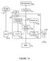
- FIG. 1Ais an example of a streaming storage drive system used according to one aspect of the present invention
- FIG. 1Bis a block diagram of a buffer controller, according to one aspect of the present invention.
- FIG. 1Cis a block diagram of a clock distribution module, according to one aspect of the present invention.
- FIG. 1Dis a block diagram of a DDR memory coupled to a controller, according to one aspect of the present invention.
- FIG. 1Eshows a SDRAM coupled to a controller, according to one aspect of the present invention
- FIG. 1Fshows a timing diagram for SDRAM signals
- FIG. 1Gshows DDR write signals used according to one aspect of the present invention
- FIG. 1His a block diagram showing an emulated DQS signal for an SDRAM operation, according to one aspect of the present invention.
- FIG. 2shows DDR logic that can also be used for SDRAM read operations using an emulated DQS signal, according to one aspect of the present invention
- FIGS. 3-6show various timing diagrams, according to one aspect of the present invention.
- FIG. 7shows a logic diagram for write operation, according to one aspect of the present invention.
- FIGS. 8-9show timing diagrams, according to one aspect of the present invention.
- the system of FIG. 1Ais an example of a streaming storage drive system (e.g., tape drive), included (or coupled to) in a computer system.
- the host computer(not shown) and the storage device 115 communicate via port 102 , which is connected to a data bus (not shown).
- the data busfor example, is a bus in accordance with a Small Computer System Interface (SCSI) specification.
- SCSISmall Computer System Interface
- the storage device 115is an external storage device, which is connected to the host computer via a data bus.
- the systemincludes controller 101 , which is coupled to SCSI port 102 , port 114 , buffer memory 111 and microprocessor 100 .
- Interface 118serves to couple microprocessor bus 107 to microprocessor 100 .
- a read only memory (“ROM”) omitted from the drawingis used to store firmware code executed by microprocessor 100 .
- Port 114couples controller 101 to device 115 .
- Controller 101can be an integrated circuit (IC) that comprises of various functional modules, which provide for the writing and reading of data stored on storage device 115 .
- Microprocessor 100is coupled to controller 101 via interface 118 to facilitate transfer of data, address, timing and control information.
- Buffer memory 111is coupled to controller 101 via ports to facilitate transfer of data, timing and address information.
- Buffer memory 111may be a DDR or SDRAM.
- Data flow controller 116is connected to microprocessor bus 107 and to buffer controller 108 .
- a DMA interface 112is connected to microprocessor bus 107 and to data and control port 113 .
- SCSI controller 105includes programmable registers and state machine sequencers that interface with SCSI port 102 on one side and to a fast, buffered direct memory access (DMA) channel on the other side.
- DMAdirect memory access
- Sequencer 106supports customized SCSI sequences, for example, by means of a 256-location instruction memory that enables users to customize command automation features. Sequencer 106 support's firmware and hardware interrupts schemes. The firmware interrupt enables microprocessor 100 to initiate an operation within Sequencer 106 without stopping sequencer operation. Hardware interrupt comes directly from SCSI controller 105 .
- Buffer controller 108connects to buffer memory 111 , DMA I/F 112 , a SCSI channel of SCSI controller 105 and bus 107 . Buffer controller 108 regulates data movement into and out of buffer memory 111 .
- a host systemsends a read command to controller 101 , which stores the read, commands in buffer memory 111 .
- Microprocessor 100then read the command out of buffer memory 111 and initializes the various functional blocks of controller 101 .
- Datais read from device 115 and is passed through DMA I/F 112 to buffer controller 108 .
- Controller 101also includes a clock distribution module (“CDM”) 120 that handles clock variation, according to one aspect of the present invention.
- FIG. 1Cshows a block diagram of CDM 120 with an oscillator 119 coupled to phased locked loop (“PLL”) 120 A that includes an electronic circuit that controls oscillator 119 so that it maintains a constant phase angle (i.e., lock) on the frequency of an input, or reference, signal.
- PLL 120 Ais coupled to a voltage regulator (“VCO”) 703 and to clock distribution logic (“CDL”) 121 that generates a buffer clock (“BUFCLK”) 701 A.
- VCOvoltage regulator
- CDLclock distribution logic
- FIG. 1Bshows a block diagram of BC 108 with Channel 1 108 A and Channel 0 108 D for moving data to and from buffer 111 .
- BC 108includes registers 108 E and an Arbiter 108 C.
- Arbiter 108 Carbitrates between plural channels in BC 108 , for example, Channel 0 108 D and Channel 1 108 A.
- Register 108 Eis coupled to interface 118 via bus 107 that allows microprocessor 100 and BC 108 to communicate.
- Data 108 G and status 108 Fis moved in and out of register 108 E.
- BC 108also includes a multi-channel memory controller 108 B that provides a common interface to either SDRAM or DDR buffer memory 111 .
- BUFCLKBuffer Clock Signal
- SDRAMCLKSDRAM Clock Signal
- DQSThis signal is used for sampling data.
- DDR Write CLKThis clock signal is used for writing to DDR 111 A:
- BD_OThis is a buffer data output signal.
- FIG. 1Dshows a top-level diagram where DDR 111 A is the buffer memory 111 .
- SDRAMCLK generated from controller 101is sent to DDR 111 A, while DQS (that is based on SDRAM CLK) and data comes from DDR 111 A for a read operation.
- DQSis sent to DDR 111 A, as described below in detail.
- DQSis a bi-directional signal.
- FIG. 1Eshows a block diagram where SDRAM 111 B is coupled to controller 101 .
- Data(“BD”) is read from SDRAM 111 B and SDRAM clock is sent from controller 101 .
- Data(“BD”) moves bi0directionally from to/from SDRAM 111 B.
- a systemsuch that a buffer clock (BUFFCLCK), SDRAM clock (SDRAMCLK) and a DDR data clock (“DQS”) are handled in such a way that the same system (or logic) can be used to support either a DDR or SDRAM version of buffer memory 111 .
- BUFFCLCKbuffer clock
- SDRAMCLKSDRAM clock
- DQSDDR data clock
- a DDR write operationis conducted using programmable delay so that data arrives at the correct time outside controller 101 .
- Data that is to be written at DDR 111 Ais moved from BUFCLK to DDR Write CLK, and DQS is appropriately delayed for data sampling, as discussed below.
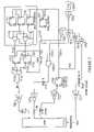
- FIG. 7shows a schematic of the logic used for a DDR write operation. It is noteworthy that the same logic is used for SDRAM write operation.
- DDR writeall signals go from controller 101 to DDR 111 A.
- the arrival time for data and DQS signal 718are based on the timing diagram shown in FIG. 8 .
- the clocksare aligned such that data lines up with the clock.
- the present inventionuses a clocking relationship instead of delaying data.
- the programmable timing delays between BUFCLK 701 A, SDRAMCLK 707 , and DQS CLK 718are provided by tap-cells 702 , 704 , 704 B and 705 that are driven by voltage controlled oscillator (“VCO”) 703 .
- VCOvoltage controlled oscillator
- Data that is written in DDR 111 Ais stored in registers 711 and 712 that are controlled by BUFCLK 701 A using logic 710 .
- registers 711 and 712are 64 bits wide to hold data. Data from registers 711 and 712 (shown as 712 A and 712 B via logic 711 A and 711 B) is moved to registers 713 and 714 that receive the DDR Write CLk 720 from tap cell 702 . Signal 720 may be delayed using cell 702 A.
- BD_O 715(data output) is generated based on inputs 713 A and 714 A from registers 713 and 714 (via multiplexer 715 A), respectively.
- I/O cell 724generates BD 716 , which is the actual data that is sent to DDR 111 A.
- DQS_O (DQS output) signal 719is generated based on DQS free running signal 704 A generated from tap cell 704 and 701 B signal from DQS enable logic 701 .
- DQS enable logic 701receives BUFCLK 701 A and generates signal 701 B to enable the DQS signal.
- Signal 704 A and 701 Bare “ANDED” by gate 720 A to generate DQS_O 719 . Thereafter, DQS_O 719 is sent to I/O cell 723 that generates DQS 718 that is sent to DDR 111 A.
- SDRAMCLK 707is generated by input/output (I/O) cell 721 based on signal 706 generated (or delayed using cell 705 A) by tap cell 705 .
- Control address logic 709receives BUFCLK 701 A and delay signal 708 from tap-cell 704 B. I/O cell 722 generates control address 722 A that is sent to DDR 111 A that determines where data is written.
- FIG. 8shows a timing diagram of various signals from FIG. 7 , according to the adaptive aspects of the present invention.
- FIG. 8shows that SDRAMCLK 707 and BUFCLK 701 A are synchronous.
- Output I/O cell delay 707 Ais based on I/O cell 721 .
- BD_O delayis based on I/O cell 724 .
- tDH ( 718 A)is the DDR data hold time based on DQS 718 for DDR writes, while tDS ( 718 B) is the data setup time based on DQS 718 for DDR writes.
- CLSK 707 Bis the clock skew between BUFCLK 701 A and SDRAMCLK 707 .
- IDQSS 718 Cis the first DQS rising edge for DDR write bursts
- tWPRE 718 Dis the time that DQS 718 is low before the first rising edge
- TWPST 718 Eis the time DQS 718 is low after the last DQS 718 falling edge.
- DDR data (shown as BD 716 in FIG. 7 ) 716is sampled (D 0 ) at the rising edge of DQS 718 and D 1 is sampled at the falling edge of 718 .
- BUFCLK 701 Ais re-timed to DDR write clock 720 that is generated by tap cell 702 .
- DQS 718is aligned to the center of BD_O 715 .
- DQS signal 718is timed so that it is later than SDRAMCLK_O 706 to provide set-up time from the start of the “data valid” window.
- the negative edge of BUFFCLK 701 Ais used to control the enabling of DQS_O clock 719 .
- the timing for DQS 718is optimum so that it is not too early or late.
- FIG. 8Ashows a simplified timing diagram with SDRAMCLK 707 , DQS 718 and data 716 signals.
- FIG. 8Ashows that data 716 is sampled at the rising and falling edge of DQS 718 and DQS 718 is approximately in the middle of data 716 .
- FIG. 1Gshows yet another simplified timing diagram showing how DQS 718 and data 716 are positioned for DDR 111 A write operation.
- FIG. 2shows a schematic of the logic that is used for reading data from DDR 111 A and SDRAM 111 B.
- DQS 209 and data 206are generated from DDR 111 A.
- the DQS 209 clock signalis generated based on SDRAMCLK 707 , which is based on input 706 to I/O cell 721 .
- DQS 209 clock signalis sent to I/O cell 208 that generates DQS_I 210 , which is delayed by cell 211 .
- DQS 209is delayed so that the DQS clock signal is centered within a valid data window.
- Registers 202 and 202 Aare used to capture data and in one aspect operate as a first in first out (“FIFO”) buffer.
- the delayed DQS 211 A signalthat is referenced as BDIN_CLK 212 and 212 B (that is generated after 211 A passes through an inverter 211 B) is used to control registers 202 and 202 A, respectively. It is noteworthy that the delay in the DQS signal may be programmed using cells 211 C and 211 D by controller 101 firmware.
- Data 206 from DDR 111 A via I/O cell 205(as output BD_I 207 ) is sent to registers 202 and 202 A, via logic 207 A and 207 B. Once data is captured in registers 202 and 202 A, it is moved (shown as 213 and 214 ) to another FIFO 201 that operates under BUFCLK 701 A.
- DQS 209 generated from DDR 111 Amay have plural alignments.
- Logic 203 and 204controls the alignment of DQS 209 based on selected latency.
- the positive edge of DQSis aligned with the positive edge of SDRAMCLK 707 generated by I/O cell 721 based on SDRAMCLK_O 706 , which is generated by VCO 703 .
- the negative edge of DQSis aligned with the negative edge.
- FIG. 3shows alignment of data with SDRAMCLK 707 within +/ ⁇ tAC nano-seconds.
- FIG. 4shows the alignment of DQS 211 A to SDRAMCLK 707 with latency CL 3 and CL 2 . 5 , respectively.
- CL 3the positive edge of DQS 211 A is aligned with the positive edge of SDRAMCLK and in CL 2 . 5 , the negative edge of DQS 211 A is aligned with the positive edge of SDRAMCLK 707 .
- the first data of the burstis valid 3 clocks after the rising edge of the read command.
- CL 2 . 5the first data of the burst is valid 2.5 clocks after the rising edge of the read command.
- the rising edge of DQS 211 Ais lined up with the leading edge of the first valid data window.
- DQS 211 Acan vary by tDQSCK 400 . Although the alignment of DQS 211 A to SDRAMCLK 707 does not directly affect the loading of data into registers 202 and 202 A, it does affect the positioning of BDIN_REG CLK 212 with respect to BUFCLK 701 A.
- FIG. 5shows a timing diagram of DQS 211 A and data 207 .
- DQS 211 Acan vary by tDQSQ 500 nano-seconds.
- FIG. 6shows the timing for data capture, where DQS 211 A is delayed to provide setup/hold margin between clock and data inputs of registers 202 and 202 A.
- TDQSQis the data skew from DQS 211 A
- tPDINis the I/O cell delay to destination
- tDQSPDis additional delay for DQS 211 A.
- SDRAM 111 Bwrite SDRAM CLK 707 that operates synchronously with BUFCLK 701 A controls operation. SDRAM CLK 707 may be delayed from BUFCLK 701 A to gain some set-up and hold time for the read operation.
- FIG. 1Fshows a timing diagram for writing data to SDRAM 111 B.
- FIG. 1Hshows a top-level block diagram for an SDRAM 111 B operation using the same logic for controller 101 .
- DQS signalis emulated for an SDRAM 111 B read operation.
- the SDRAM clock 707is fed into the DQS signal, which then becomes the emulated DQS signal.
- For an SDRAM 111 B read operationonly the positive edge flop 202 (also shown in FIG. 2 ) is used.
- both 202 and 202 Aare used.
- SDRAM read operationis synchronous with SDRAMCLK 707 and BUFCLK 701 A.
- the data read delay (tSDRAC) from SDRAM 111 Bis equal to the clock period.
- FIG. 9shows the timing diagram for SDRAM 111 B read operation at 183 MHz. It is noteworthy that the present invention is not limited to any particular frequency rate.
- FIG. 9shows SDRAMCLK 707 , BUFCLK 701 A, data (“BD”) and BDIN Clock signal (derived from BUFCLK).
- tSDRACis the time SDRAM 111 B data read output delay
- tSDROHis the SDRAM data read output data hold-time
- tPDINis the input I/O cell delay to destination.
- the same logicis used to read and/or write data to DDR or SDRAM, hence overall controller cost is reduced.
Landscapes
- Engineering & Computer Science (AREA)
- Theoretical Computer Science (AREA)
- Physics & Mathematics (AREA)
- General Engineering & Computer Science (AREA)
- General Physics & Mathematics (AREA)
- Dram (AREA)
Abstract
Description
This application is a Continuation of U.S. patent application Ser. No. 11/542,862, filed Oct. 4, 2006, now U.S. Pat. No. 7,286,441 which is a continuation of U.S. patent application Ser. No. 10/867,113 filed on Jun. 14, 2004 now U.S. Pat. No. 7,120,084. The disclosures of the above applications are incorporated herein by reference.
1. Field of the Invention
The present invention relates generally to storage device controllers, and more particularly, to integrated memory controllers.
2. Background
Conventional computer systems typically include several functional components. These components may include a central processing unit (CPU), main memory, input/output (“I/O”) devices, and streaming storage devices (for example, tape drives) (referred to herein as “storage device”). In conventional systems, the main memory is coupled to the CPU via a system bus or a local memory bus. The main memory is used to provide the CPU access to data and/or program information that is stored in main memory at execution time. Typically, the main memory is composed of random access memory (RAM) circuits. A computer system with the CPU and main memory is often referred to as a host system.
The storage device is coupled to the host system via a controller that handles complex details of interfacing the storage devices to the host system. Communications between the host system and the controller is usually provided using one of a variety of standard I/O bus interfaces.
Typically, when data is read from a storage device, a host system sends a read command to the controller, which stores the read command into the buffer memory. Data is read from the device and stored in the buffer memory.
Buffer memory may be a Synchronous Dynamic Random access Memory (“SDRAM”), or Double Data Rate-Synchronous Dynamic Random Access Memory (referred to as “DDR”). In SDRAM communication occurs at the positive end of a clock signal, i.e. data is received and read at the positive edge of a clock. Hence, SDRAM is a single data rate memory device.
DDR is a type of SDRAM that supports data transfers on both edges of each clock cycle (the rising and falling edges), effectively doubling the memory chip's data throughput. In DDR address and commands are similar to SDRAM, but the data is handled differently by using a separate clock (“DQS”). DQS is used for receiving and sending data from the DDR.
Modern storage systems may use either SDRAM or DDR and it is desirable to have a single interface that supports both DDR and SDRAM read and write operations. Conventional systems do not provide this option.
Therefore, there is a need for a method and system to support both DDR and SDRAM using the same hardware in the controller.
A system for writing data to a buffer memory, which is Synchronous Dynamic Random access Memory (“SDRAM”), or Double Data Rate-Synchronous Dynamic Random Access Memory (“DDR”) is provided. The system includes, means for managing programmable clock signal relationships such that data arrives at an optimum time for writing. Data that is to be written at DDR is moved from a first buffer clock to a DDR write clock and to a DQS signal that is based on a SDRAM clock signal.
A circuit for writing data to a buffer memory, which is Synchronous Dynamic Random access Memory (“SDRAM”), or Double Data Rate-Synchronous Dynamic Random Access Memory (“DDR”) is provided. The circuit includes logic for managing programmable clock signal relationships such that data arrives at an optimum time for writing. Data that is to be written at DDR is moved from a first buffer clock to a DDR write clock signal and to a DQS signal that is based on a SDRAM clock signal. Also, plural tap-cells may be used to delay clock signals such that data and clock signals are aligned.
A circuit for reading data from a buffer memory, which is Synchronous Dynamic Random access Memory (“SDRAM”), or Double Data Rate-Synchronous Dynamic Random Access Memory (“DDR”) is provided. The circuit includes logic for managing programmable clock signal relationships such that data that is read from the DDR is centered within a DQS signal, which is generated from the DDR and then appropriately delayed. The DQS signal is delayed with respect to the data that is read from the DDR and data from the DDR is placed in a register that is controlled by a delayed DQS signal.
A system for reading data from a buffer memory, which is Synchronous Dynamic Random access Memory (“SDRAM”), or Double Data Rate-Synchronous Dynamic Random Access Memory (“DDR”) is provided. The system includes means for managing programmable clock signal relationships such that data that is read from the DDR is centered within a DQS signal generated from the DDR and then appropriately delayed. The DQS signal is delayed with respect to the data that is read from the DDR and data from the DDR is placed in a register that is controlled by a delayed DQS signal. Also, an emulated DQS signal in an SDRAM clock signal is used for reading from a SDRAM and a DDR capture scheme is used for reading data from an SDRAM.
This brief summary has been provided so that the nature of the invention may be understood quickly. A more complete understanding of the invention can be obtained by reference to the following detailed description of the preferred embodiments thereof concerning the attached drawings.
The foregoing features and other features of the present invention will now be described with reference to the drawings of a preferred embodiment. In the drawings, the same components have the same reference numerals. The illustrated embodiment is intended to illustrate, but not to limit the invention. The drawings include the following Figures:
To facilitate an understanding of the preferred embodiment, the general architecture and operation of a controller will initially be described. The specific architecture and operation of the preferred embodiment will then be described with reference to the general architecture.
The system ofFIG. 1A is an example of a streaming storage drive system (e.g., tape drive), included (or coupled to) in a computer system. The host computer (not shown) and thestorage device 115 communicate viaport 102, which is connected to a data bus (not shown). The data bus, for example, is a bus in accordance with a Small Computer System Interface (SCSI) specification. Those skilled in the art will appreciate that other communication buses known in the art can be used to transfer data between the drive and the host system. In an alternate embodiment (not shown), thestorage device 115 is an external storage device, which is connected to the host computer via a data bus.
As shown inFIG. 1A , the system includescontroller 101, which is coupled toSCSI port 102,port 114,buffer memory 111 andmicroprocessor 100.Interface 118 serves to couplemicroprocessor bus 107 tomicroprocessor 100. A read only memory (“ROM”) omitted from the drawing is used to store firmware code executed bymicroprocessor 100.Port 114couples controller 101 todevice 115.
SCSI controller105 includes programmable registers and state machine sequencers that interface withSCSI port 102 on one side and to a fast, buffered direct memory access (DMA) channel on the other side.
Buffer controller (also referred to as “BC”)108 connects to buffermemory 111, DMA I/F 112, a SCSI channel of SCSI controller105 andbus 107.Buffer controller 108 regulates data movement into and out ofbuffer memory 111.
To read data fromstorage device 115, a host system sends a read command tocontroller 101, which stores the read, commands inbuffer memory 111.Microprocessor 100 then read the command out ofbuffer memory 111 and initializes the various functional blocks ofcontroller 101. Data is read fromdevice 115 and is passed through DMA I/F 112 to buffercontroller 108.
Before describing the adaptive aspects of the present invention, the following describes some of the clock signals that are used forbuffer 111 read and write operations:
BUFCLK (Buffer Clock Signal): This is a clock signal that is used for running various modules of thememory controller 108B.
SDRAMCLK (SDRAM Clock Signal): This is a clock signal forSDRAM 111B.
DQS: This signal is used for sampling data.
DDR Write CLK: This clock signal is used for writing toDDR 111A:
BD_O: This is a buffer data output signal.
In one aspect of the present invention, a system is provided such that a buffer clock (BUFFCLCK), SDRAM clock (SDRAMCLK) and a DDR data clock (“DQS”) are handled in such a way that the same system (or logic) can be used to support either a DDR or SDRAM version ofbuffer memory 111.
DDR Write Operation:
In one aspect of the present invention a DDR write operation is conducted using programmable delay so that data arrives at the correct time outsidecontroller 101. Data that is to be written atDDR 111A is moved from BUFCLK to DDR Write CLK, and DQS is appropriately delayed for data sampling, as discussed below.
For DDR write, all signals go fromcontroller 101 toDDR 111A. The arrival time for data and DQS signal718 are based on the timing diagram shown inFIG. 8 . The clocks are aligned such that data lines up with the clock. The present invention uses a clocking relationship instead of delaying data. The programmable timing delays betweenBUFCLK 701A,SDRAMCLK 707, andDQS CLK 718 are provided by tap-cells
Data that is written inDDR 111A is stored inregisters BUFCLK 701 A using logic 710. In one aspect, registers711 and712 are 64 bits wide to hold data. Data fromregisters 711 and712 (shown as712A and712B vialogic registers DDR Write CLk 720 fromtap cell 702.Signal 720 may be delayed using cell702A.
BD_O715 (data output) is generated based oninputs registers 713 and714 (viamultiplexer 715A), respectively.
Input/Output (“I/O”)cell 724 generatesBD 716, which is the actual data that is sent toDDR 111A.
DQS_O (DQS output) signal719 is generated based on DQSfree running signal 704A generated fromtap cell logic 701. DQS enablelogic 701 receivesBUFCLK 701A and generates signal701B to enable the DQS signal.Signal gate 720A to generateDQS_O 719. Thereafter,DQS_O 719 is sent to I/O cell 723 that generatesDQS 718 that is sent toDDR 111A.
DDR Read Operation:
SDRAM Write Operation:
SDRAM Read Operation:
SDRAM read operation is synchronous withSDRAMCLK 707 andBUFCLK 701A. In some instances, for example, at 183 MHZ, the data read delay (tSDRAC) fromSDRAM 111B is equal to the clock period.FIG. 9 shows the timing diagram forSDRAM 111B read operation at 183 MHz. It is noteworthy that the present invention is not limited to any particular frequency rate.FIG. 9 showsSDRAMCLK 707,BUFCLK 701A, data (“BD”) and BDIN Clock signal (derived from BUFCLK). “tSDRAC” is thetime SDRAM 111B data read output delay; “tSDROH” is the SDRAM data read output data hold-time; and “tPDIN” is the input I/O cell delay to destination.
In one aspect of the present invention, the same logic is used to read and/or write data to DDR or SDRAM, hence overall controller cost is reduced.
Although the present invention has been described with reference to specific embodiments, these embodiments are illustrative only and not limiting. Many other applications and embodiments of the present invention will be apparent in light of this disclosure.
Claims (20)
1. A memory system comprising:
memory that includes Synchronous Dynamic Random Access Memory (SDRAM); and
a memory controller that:
communicates with the memory;
generates an SDRAM clock signal;
receives a bi-directional sampling clock signal (DQS) that is generated based on the SDRAM clock signal; and
reads data from the memory based on the DQS,
wherein the memory controller generates the SDRAM clock signal based on a buffer clock signal.
2. The memory system ofclaim 1 wherein the memory controller reads the data from the SDRAM further based on at least one of the SDRAM clock signal and the buffer clock signal.
3. The memory system ofclaim 1 wherein the memory controller writes the data to the SDRAM based on at least one of the SDRAM clock signal and the buffer clock signal.
4. The memory system ofclaim 1 further comprising a clock distribution module that generates the buffer clock signal.
5. A memory system comprising:
memory that includes Synchronous Dynamic Random Access Memory (SDRAM); and
a memory controller that:
communicates with the memory;
generates an SDRAM clock signal;
receives a bi-directional sampling clock signal (DQS) that is generated based on the SDRAM clock signal; and
reads data from the memory based on the DQS.
wherein the SDRAM clock signal emulates the DQS.
6. A memory system comprising:
memory that includes Synchronous Dynamic Random Access Memory (SDRAM);
a memory controller that:
communicates with the memory;
generates an SDRAM clock signal;
receives a bi-directional sampling clock signal (DQS) that is generated based on the SDRAM clock signal; and
reads data from the memory based on the DQS; and
logic that is connected between the memory and the memory controller and that aligns the DQS to the data based on a delay.
7. The memory system ofclaim 6 wherein the logic includes at least one programmable delay element.
8. A memory system comprising:
memory means for including Synchronous Dynamic Random Access Memory (SDRAM); and
memory controller means for communicating with the memory means, for generating an SDRAM clock signal, for receiving a bi-directional sampling clock signal (DQS) that is generated based on the SDRAM clock signal, and for reading data from the memory means based on the DQS,
wherein the memory controller means generates the SDRAM clock signal based on a buffer clock signal.
9. The memory system ofclaim 8 wherein the memory controller means reads the data from the SDRAM further based on at least one of the SDRAM clock signal and the buffer clock signal.
10. The memory system ofclaim 8 wherein the memory controller means writes the data to the SDRAM based on at least one of the SDRAM clock signal and the buffer clock signal.
11. The memory system ofclaim 8 further comprising clock distribution means for generating the buffer clock signal.
12. A memory system comprising:
memory means for including Synchronous Dynamic Random Access Memory (SDRAM); and
memory controller means for communicating with the memory means, for generating an SDRAM clock signal, for receiving a bi-directional sampling clock signal (DQS) that is generated based on the SDRAM clock signal, and for reading data from the memory means based on the DQS,
wherein the SDRAM clock signal emulates the DQS.
13. A memory system comprising:
memory means for including Synchronous Dynamic Random Access Memory (SDRAM);
memory controller means for communicating with the memory means, for generating an SDRAM clock signal, for receiving a bi-directional sampling clock signal (DQS) that is generated based on the SDRAM clock signal, and for reading data from the memory means based on the DQS; and
logic means, connected between the memory means and the memory controller means, for aligning the DQS to the data based on a delay.
14. The memory system ofclaim 13 wherein the logic means includes at least one programmable delay element.
15. A method for operating a memory controller to interface with each of Synchronous Dynamic Random Access Memory (SDRAM) and Double Data Rate SDRAM (DDR) comprising:
providing SDRAM;
generating the SDRAM clock signal with the memory controller based on a buffer clock signal;
receiving a bi-directional sampling clock signal (DQS) that is generated based on the SDRAM clock signal at the memory controller; and
reading data from the SDRAM based on the DQS.
16. The method ofclaim 15 wherein the reading the data from the SDRAM includes reading the data further based on at least one of the SDRAM clock signal and the buffer clock signal.
17. The method ofclaim 15 wherein further comprising writing the data to the SDRAM based on at least one of the SDRAM clock signal and the buffer clock signal.
18. The method ofclaim 15 further comprising generating the buffer clock signal with a clock distribution module.
19. A method for operating a memory controller to interface with each of Synchronous Dynamic Random Access Memory (SDRAM) and Double Data Rate SDRAM (DDR) comprising:
providing SDRAM;
generating an SDRAM clock signal with the memory controller;
receiving a bi-directional sampling clock signal (DQS) that is generated based on the SDRAM clock signal at the memory controller; and
reading data from the SDRAM based on the DQS,
wherein the SDRAM clock signal emulates the DQS.
20. A method for operating a memory controller to interface with each of Synchronous Dynamic Random Access Memory (SDRAM) and Double Data Rate SDRAM (DDR) comprising:
providing SDRAM;
generating an SDRAM clock signal with the memory controller;
receiving a bi-directional sampling clock signal (DQS) that is generated based on the SDRAM clock signal at the memory controller;
reading data from the SDRAM based on the DQS; and
aligning the DQS to the data based on a delay.
Priority Applications (1)
| Application Number | Priority Date | Filing Date | Title |
|---|---|---|---|
| US11/977,169US7535791B1 (en) | 2004-06-14 | 2007-10-23 | Integrated memory controller |
Applications Claiming Priority (3)
| Application Number | Priority Date | Filing Date | Title |
|---|---|---|---|
| US10/867,113US7120084B2 (en) | 2004-06-14 | 2004-06-14 | Integrated memory controller |
| US11/542,862US7286441B1 (en) | 2004-06-14 | 2006-10-04 | Integrated memory controller |
| US11/977,169US7535791B1 (en) | 2004-06-14 | 2007-10-23 | Integrated memory controller |
Related Parent Applications (1)
| Application Number | Title | Priority Date | Filing Date |
|---|---|---|---|
| US11/542,862ContinuationUS7286441B1 (en) | 2004-06-14 | 2006-10-04 | Integrated memory controller |
Publications (1)
| Publication Number | Publication Date |
|---|---|
| US7535791B1true US7535791B1 (en) | 2009-05-19 |
Family
ID=35460396
Family Applications (4)
| Application Number | Title | Priority Date | Filing Date |
|---|---|---|---|
| US10/867,113Expired - LifetimeUS7120084B2 (en) | 2004-06-14 | 2004-06-14 | Integrated memory controller |
| US11/542,862Expired - LifetimeUS7286441B1 (en) | 2004-06-14 | 2006-10-04 | Integrated memory controller |
| US11/542,726Expired - LifetimeUS7596053B1 (en) | 2004-06-14 | 2006-10-04 | Integrated memory controller |
| US11/977,169Expired - LifetimeUS7535791B1 (en) | 2004-06-14 | 2007-10-23 | Integrated memory controller |
Family Applications Before (3)
| Application Number | Title | Priority Date | Filing Date |
|---|---|---|---|
| US10/867,113Expired - LifetimeUS7120084B2 (en) | 2004-06-14 | 2004-06-14 | Integrated memory controller |
| US11/542,862Expired - LifetimeUS7286441B1 (en) | 2004-06-14 | 2006-10-04 | Integrated memory controller |
| US11/542,726Expired - LifetimeUS7596053B1 (en) | 2004-06-14 | 2006-10-04 | Integrated memory controller |
Country Status (1)
| Country | Link |
|---|---|
| US (4) | US7120084B2 (en) |
Cited By (1)
| Publication number | Priority date | Publication date | Assignee | Title |
|---|---|---|---|---|
| US20090323730A1 (en)* | 2008-04-18 | 2009-12-31 | Honeywell International Inc. | Data alignment system and method for double data rate input data stream |
Families Citing this family (18)
| Publication number | Priority date | Publication date | Assignee | Title |
|---|---|---|---|---|
| US7301831B2 (en) | 2004-09-15 | 2007-11-27 | Rambus Inc. | Memory systems with variable delays for write data signals |
| TWI299169B (en)* | 2006-02-24 | 2008-07-21 | Realtek Semiconductor Corp | Signal sampling apparatus and method for dram memory |
| JP5132074B2 (en)* | 2006-04-13 | 2013-01-30 | オンセミコンダクター・トレーディング・リミテッド | Memory access device |
| US8572302B1 (en) | 2006-10-13 | 2013-10-29 | Marvell International Ltd. | Controller for storage device with improved burst efficiency |
| US7752356B1 (en) | 2006-10-26 | 2010-07-06 | Marvell International Ltd. | Buffer management system and method |
| US20080158601A1 (en)* | 2006-12-29 | 2008-07-03 | Steven Tu | Image memory tiling |
| KR100929845B1 (en)* | 2007-09-28 | 2009-12-04 | 주식회사 하이닉스반도체 | Synchronous semiconductor memory device and driving method thereof |
| US7675811B2 (en)* | 2008-04-07 | 2010-03-09 | Chipx Incorporated | Method and apparatus for DQS postamble detection and drift compensation in a double data rate (DDR) physical interface |
| US9106592B1 (en) | 2008-05-18 | 2015-08-11 | Western Digital Technologies, Inc. | Controller and method for controlling a buffered data transfer device |
| US8094397B2 (en)* | 2009-01-07 | 2012-01-10 | International Business Machines Corporation | System, method, and computer program product for characterizing media associated with data storage channels |
| US8345490B2 (en) | 2010-06-23 | 2013-01-01 | International Business Machines Corporation | Split voltage level restore and evaluate clock signals for memory address decoding |
| US8599642B2 (en) | 2010-06-23 | 2013-12-03 | International Business Machines Corporation | Port enable signal generation for gating a memory array device output |
| US8351278B2 (en) | 2010-06-23 | 2013-01-08 | International Business Machines Corporation | Jam latch for latching memory array output data |
| US8345497B2 (en) | 2010-06-23 | 2013-01-01 | International Business Machines Corporation | Internal bypassing of memory array devices |
| US9171846B2 (en) | 2012-05-31 | 2015-10-27 | Moon J. Kim | Leakage and performance graded memory |
| CN108763116B (en)* | 2018-05-21 | 2021-08-06 | 南京大学 | A Multi-Channel DDR Controller Based on Greedy Algorithm |
| CN118366514A (en)* | 2023-01-12 | 2024-07-19 | 长鑫存储技术有限公司 | Write leveling system and write leveling method |
| CN118692528B (en)* | 2024-06-11 | 2025-04-11 | 海光云芯集成电路设计(上海)有限公司 | Method for optimizing transmission signal of memory, memory controller and electronic equipment |
Citations (201)
| Publication number | Priority date | Publication date | Assignee | Title |
|---|---|---|---|---|
| US3800281A (en) | 1972-12-26 | 1974-03-26 | Ibm | Error detection and correction systems |
| US3823393A (en) | 1972-10-02 | 1974-07-09 | Little Inc A | Data transfer device for word processing system |
| US3836891A (en) | 1973-07-05 | 1974-09-17 | Bendix Corp | Tape reader system with buffer memory |
| US3988716A (en) | 1974-08-05 | 1976-10-26 | Nasa | Computer interface system |
| US4001883A (en) | 1974-03-07 | 1977-01-04 | Honeywell Information Systems, Inc. | High density data storage on magnetic disk |
| US4002827A (en) | 1975-05-15 | 1977-01-11 | General Electric Company | Polar coordinate format to a cartesian coordinate format scan converter |
| US4016368A (en) | 1975-12-12 | 1977-04-05 | North Electric Company | Framing circuit for digital receiver |
| US4050097A (en) | 1976-09-27 | 1977-09-20 | Honeywell Information Systems, Inc. | Synchronization technique for data transfers over an asynchronous common bus network coupling data processing apparatus |
| US4080649A (en) | 1976-12-16 | 1978-03-21 | Honeywell Information Systems Inc. | Balancing the utilization of I/O system processors |
| US4156867A (en) | 1977-09-06 | 1979-05-29 | Motorola, Inc. | Data communication system with random and burst error protection and correction |
| US4225960A (en) | 1979-03-01 | 1980-09-30 | Westinghouse Electric Corp. | Automatic synchronizing system for digital asynchronous communications |
| US4275457A (en) | 1977-05-18 | 1981-06-23 | Martin Marietta Corporation | Apparatus and method for receiving digital data at a first rate and outputting the data at a different rate |
| US4390969A (en) | 1980-04-21 | 1983-06-28 | Burroughs Corporation | Asynchronous data transmission system with state variable memory and handshaking protocol circuits |
| US4451898A (en) | 1981-11-09 | 1984-05-29 | Hewlett-Packard Company | Asynchronous interface message transmission using source and receive devices |
| US4486750A (en) | 1981-05-18 | 1984-12-04 | Takeda Riken Co. Ltd. | Data transfer system |
| US4500926A (en) | 1981-06-17 | 1985-02-19 | Tokyo Shibaura Denki Kabushiki Kaisha | Data-recording apparatus |
| US4587609A (en) | 1983-07-01 | 1986-05-06 | Honeywell Information Systems Inc. | Lockout operation among asynchronous accessers of a shared computer system resource |
| US4603382A (en) | 1984-02-27 | 1986-07-29 | International Business Machines Corporation | Dynamic buffer reallocation |
| US4625321A (en) | 1985-05-23 | 1986-11-25 | Standard Microsystems Corporation | Dual edge clock address mark detector |
| US4667286A (en) | 1984-12-20 | 1987-05-19 | Advanced Micro Devices, Inc. | Method and apparatus for transferring data between a disk and a central processing unit |
| US4680647A (en) | 1983-09-26 | 1987-07-14 | Pioneer Electronic Corporation | Method for recording and reproducing video format signal |
| US4777635A (en) | 1986-08-08 | 1988-10-11 | Data Systems Technology Corp. | Reed-Solomon code encoder and syndrome generator circuit |
| JPS63292462A (en) | 1987-05-25 | 1988-11-29 | Ricoh Co Ltd | Format system for magnetic disk device |
| US4805046A (en) | 1985-10-28 | 1989-02-14 | Matsushita Electric Industrial Co., Ltd. | Information recording and reproducing apparatus using sectors divided into a plurality of frames and having means for proper storage of the frame data |
| US4807116A (en) | 1976-09-07 | 1989-02-21 | Tandem Computers Incorporated | Interprocessor communication |
| US4807253A (en) | 1987-11-13 | 1989-02-21 | American Telephone And Telegraph Company, At&T Bell Laboratories | Time-varying trellis-coded modulation formats which are robust in channels with phase variations |
| US4809091A (en) | 1986-04-16 | 1989-02-28 | Hitachi, Ltd. | Disk apparatus |
| US4811282A (en) | 1985-12-18 | 1989-03-07 | Sgs Mircroelettronica Spa | Retiming circuit for pulse signals, particularly for microprocessor peripherals |
| US4812769A (en) | 1986-04-30 | 1989-03-14 | Tektronix, Inc. | Programmable sampling time base circuit |
| US4860333A (en) | 1986-03-12 | 1989-08-22 | Oread Laboratories, Inc. | Error protected central control unit of a switching system and method of operation of its memory configuration |
| US4866606A (en) | 1984-06-22 | 1989-09-12 | Austria Miktosystem International Gmbh | Loosely coupled distributed computer system with node synchronization for precision in real time applications |
| US4881232A (en) | 1987-02-10 | 1989-11-14 | Sony Corporation | Method and apparatus for error correction |
| JPH01315071A (en) | 1988-06-13 | 1989-12-20 | Nec Corp | Magnetic disk device |
| US4920535A (en) | 1987-12-14 | 1990-04-24 | Fujitsu Limited | Demultiplexer system |
| US4949342A (en) | 1987-04-14 | 1990-08-14 | Matsushita Electric Industrial Co., Ltd. | Code error detecting method |
| US4970418A (en) | 1989-09-26 | 1990-11-13 | Apple Computer, Inc. | Programmable memory state machine for providing variable clocking to a multimode memory |
| US4972417A (en) | 1988-06-24 | 1990-11-20 | Sony Corporation | PCM data transmitting apparatus and method |
| US4975915A (en) | 1987-04-19 | 1990-12-04 | Sony Corporation | Data transmission and reception apparatus and method |
| US4989190A (en) | 1987-07-20 | 1991-01-29 | Oki Electric Industry Co., Ltd. | Apparatus for seeking a track of an optical disk in which information is recorded |
| US5014186A (en) | 1986-08-01 | 1991-05-07 | International Business Machines Corporation | Data-processing system having a packet transfer type input/output system |
| US5023612A (en) | 1989-07-13 | 1991-06-11 | Pacific Bell | Illegal sequence detection and protection circuit |
| US5027357A (en) | 1988-10-14 | 1991-06-25 | Advanced Micro Devices, Inc. | ECC/CRC error detection and correction system |
| JPH03183067A (en) | 1989-12-11 | 1991-08-09 | Fujitsu Ltd | Magnetic disk device |
| US5050013A (en) | 1989-12-04 | 1991-09-17 | Seagate Technology, Inc. | Hard sectoring circuit and method for a rotating disk data storage device |
| US5051998A (en) | 1988-06-28 | 1991-09-24 | Matsushita Electric Industrial Co., Ltd. | Data block deinterleaving and error correction system |
| US5068755A (en) | 1990-06-01 | 1991-11-26 | Micropolis Corporation | Sector pulse generator for hard disk drive assembly |
| US5068857A (en) | 1988-09-02 | 1991-11-26 | Mitsubishi Denki Kabushiki Kaisha | Error correction circuit |
| US5072420A (en) | 1989-03-16 | 1991-12-10 | Western Digital Corporation | FIFO control architecture and method for buffer memory access arbitration |
| US5088093A (en) | 1986-04-18 | 1992-02-11 | Cias, Inc. | Self-correcting registers, error-detecting/correcting registers, and inversion coding using one bit, and other information storage media |
| US5109500A (en) | 1986-10-31 | 1992-04-28 | Hitachi, Ltd. | Disk drive control unit having sets of operating command and operation length information and generating end signal based upon operation length information |
| US5117442A (en) | 1988-12-14 | 1992-05-26 | National Semiconductor Corporation | Methods and circuits for synchronizing signals in a modular redundant fault tolerant computer system |
| US5127098A (en) | 1989-04-12 | 1992-06-30 | Sun Microsystems, Inc. | Method and apparatus for the context switching of devices |
| US5133062A (en) | 1986-03-06 | 1992-07-21 | Advanced Micro Devices, Inc. | RAM buffer controller for providing simulated first-in-first-out (FIFO) buffers in a random access memory |
| US5136592A (en) | 1989-06-28 | 1992-08-04 | Digital Equipment Corporation | Error detection and correction system for long burst errors |
| US5146585A (en) | 1988-10-25 | 1992-09-08 | International Business Machines Corporation | Synchronized fault tolerant clocks for multiprocessor systems |
| US5157669A (en) | 1988-10-14 | 1992-10-20 | Advanced Micro Devices, Inc. | Comparison of an estimated CRC syndrome to a generated CRC syndrome in an ECC/CRC system to detect uncorrectable errors |
| US5162954A (en) | 1990-07-31 | 1992-11-10 | Seagate Technology Inc. | Apparatus for generating an index pulse in a data storage system |
| US5193197A (en) | 1987-09-24 | 1993-03-09 | Digital Equipment Corporation | Apparatus and method for distributed dynamic priority arbitration for access to a shared resource |
| US5204859A (en) | 1990-02-23 | 1993-04-20 | Gec Plessey Telecommunications Limited | Method and apparatus for detecting a frame alignment word in a data system |
| US5218564A (en) | 1991-06-07 | 1993-06-08 | National Semiconductor Corporation | Layout efficient 32-bit shifter/register with 16-bit interface |
| US5220569A (en) | 1990-07-09 | 1993-06-15 | Seagate Technology, Inc. | Disk array with error type indication and selection of error correction method |
| US5237593A (en) | 1989-05-04 | 1993-08-17 | Stc, Plc | Sequence synchronisation |
| US5243471A (en) | 1991-01-10 | 1993-09-07 | Hewlett-Packard Company | Method and apparatus for detecting a start of data position in differing tracks |
| US5249271A (en) | 1990-06-04 | 1993-09-28 | Emulex Corporation | Buffer memory data flow controller |
| US5257143A (en) | 1991-01-15 | 1993-10-26 | Zenith Data Systems Corporation | Method and apparatus for positioning head of disk drive using zone-bit-recording |
| US5261081A (en) | 1990-07-26 | 1993-11-09 | Ncr Corporation | Sequence control apparatus for producing output signals in synchronous with a consistent delay from rising or falling edge of clock input signal |
| US5271018A (en) | 1990-04-27 | 1993-12-14 | Next, Inc. | Method and apparatus for media defect management and media addressing |
| US5274509A (en) | 1992-09-10 | 1993-12-28 | Digital Equipment Corporation | On-the-fly splitting of disk data blocks using timed sampling of a data position indicator |
| US5276662A (en) | 1992-10-01 | 1994-01-04 | Seagate Technology, Inc. | Disc drive with improved data transfer management apparatus |
| US5276564A (en) | 1992-04-16 | 1994-01-04 | Hewlett-Packard Company | Programmable start-of-sector pulse generator for a disk drive using embedded servo bursts and split data fields |
| US5276807A (en) | 1987-04-13 | 1994-01-04 | Emulex Corporation | Bus interface synchronization circuitry for reducing time between successive data transmission in a system using an asynchronous handshaking |
| US5280488A (en) | 1990-11-08 | 1994-01-18 | Neal Glover | Reed-Solomon code system employing k-bit serial techniques for encoding and burst error trapping |
| US5285327A (en) | 1990-01-17 | 1994-02-08 | International Business Machines Corporation | Apparatus for controlling reading and writing in a disk drive |
| US5285451A (en) | 1990-04-06 | 1994-02-08 | Micro Technology, Inc. | Failure-tolerant mass storage system |
| US5301333A (en) | 1990-06-14 | 1994-04-05 | Bell Communications Research, Inc. | Tree structured variable priority arbitration implementing a round-robin scheduling policy |
| US5307216A (en) | 1991-09-04 | 1994-04-26 | International Business Machines Corporation | Sector identification method and apparatus for a direct access storage device |
| US5315708A (en) | 1990-02-28 | 1994-05-24 | Micro Technology, Inc. | Method and apparatus for transferring data through a staging memory |
| US5339443A (en) | 1991-11-19 | 1994-08-16 | Sun Microsystems, Inc. | Arbitrating multiprocessor accesses to shared resources |
| US5361266A (en) | 1992-11-04 | 1994-11-01 | Mitsubishi Denki Kabushiki Kaisha | Error correction circuit |
| US5361267A (en) | 1992-04-24 | 1994-11-01 | Digital Equipment Corporation | Scheme for error handling in a computer system |
| EP0622726A2 (en) | 1993-04-30 | 1994-11-02 | Quantum Corporation | Shared memory array for data block and control program storage in disk drive |
| US5408644A (en) | 1992-06-05 | 1995-04-18 | Compaq Computer Corporation | Method and apparatus for improving the performance of partial stripe operations in a disk array subsystem |
| US5410554A (en) | 1992-03-23 | 1995-04-25 | Kabushiki Kaisha Toshiba | Optical disk apparatus |
| US5420984A (en) | 1992-06-30 | 1995-05-30 | Genroco, Inc. | Apparatus and method for rapid switching between control of first and second DMA circuitry to effect rapid switching beween DMA communications |
| US5428627A (en) | 1992-11-10 | 1995-06-27 | Qlogic Corporation | Method and apparatus for initializing an ECC circuit |
| US5440751A (en) | 1991-06-21 | 1995-08-08 | Compaq Computer Corp. | Burst data transfer to single cycle data transfer conversion and strobe signal conversion |
| US5450546A (en) | 1992-01-31 | 1995-09-12 | Adaptec, Inc. | Intelligent hardware for automatically controlling buffer memory storage space in a disk drive |
| US5487170A (en) | 1993-12-16 | 1996-01-23 | International Business Machines Corporation | Data processing system having dynamic priority task scheduling capabilities |
| US5488688A (en) | 1994-03-30 | 1996-01-30 | Motorola, Inc. | Data processor with real-time diagnostic capability |
| US5491701A (en) | 1993-11-04 | 1996-02-13 | Cirrus Logic, Inc. | Burst error corrector |
| US5500848A (en) | 1991-07-10 | 1996-03-19 | International Business Machines Corporation | Sector servo data recording disk having data regions without identification (ID) fields |
| US5506989A (en) | 1990-01-31 | 1996-04-09 | Ibm Corporation | Arbitration system limiting high priority successive grants |
| US5507005A (en) | 1991-03-18 | 1996-04-09 | Hitachi, Ltd. | Data transferring system between host and I/O using a main buffer with sub-buffers where quantity of data in sub-buffers determine access requests |
| US5519837A (en) | 1994-07-29 | 1996-05-21 | International Business Machines Corporation | Pseudo-round-robin arbitration for a shared resource system providing fairness and high throughput |
| US5523903A (en) | 1993-12-23 | 1996-06-04 | International Business Machines Corporation | Sector architecture for fixed block disk drive |
| US5544346A (en) | 1992-01-02 | 1996-08-06 | International Business Machines Corporation | System having a bus interface unit for overriding a normal arbitration scheme after a system resource device has already gained control of a bus |
| US5544180A (en) | 1992-06-08 | 1996-08-06 | Qlogic Corporation | Error-tolerant byte synchronization recovery scheme |
| US5546545A (en) | 1994-12-09 | 1996-08-13 | International Business Machines Corporation | Rotating priority selection logic circuit |
| US5546548A (en) | 1993-03-31 | 1996-08-13 | Intel Corporation | Arbiter and arbitration process for a dynamic and flexible prioritization |
| US5563896A (en) | 1991-01-22 | 1996-10-08 | Fujitsu Limited | Error correction processor and an error correcting method |
| US5572148A (en) | 1995-03-22 | 1996-11-05 | Altera Corporation | Programmable logic array integrated circuit with general-purpose memory configurable as a random access or FIFO memory |
| US5574867A (en) | 1994-07-08 | 1996-11-12 | Intel Corporation | Fast first-come first served arbitration method |
| US5581715A (en) | 1994-06-22 | 1996-12-03 | Oak Technologies, Inc. | IDE/ATA CD drive controller having a digital signal processor interface, dynamic random access memory, data error detection and correction, and a host interface |
| US5583999A (en) | 1994-01-14 | 1996-12-10 | Fujitsu Limited | Bus arbiter and bus arbitrating method |
| US5592404A (en) | 1993-11-04 | 1997-01-07 | Cirrus Logic, Inc. | Versatile error correction system |
| US5600662A (en) | 1993-09-21 | 1997-02-04 | Cirrus Logic, Inc. | Error correction method and apparatus for headers |
| US5623672A (en) | 1994-12-23 | 1997-04-22 | Cirrus Logic, Inc. | Arrangement and method of arbitration for a resource with shared user request signals and dynamic priority assignment |
| US5626949A (en) | 1994-04-04 | 1997-05-06 | Blauer Manufacturing Company | Breathable shell for outerwear |
| US5627695A (en) | 1995-01-12 | 1997-05-06 | Qlogic Corporation | System and method for generating unique sector identifiers for an identificationless disk format |
| US5640602A (en) | 1994-06-10 | 1997-06-17 | Fujitsu Limited | Transferring digital data in units of 2 bytes to increase utilization of a 2-byte-wide bus |
| US5649230A (en) | 1992-03-31 | 1997-07-15 | Seiko Epson Corporation | System for transferring data using value in hardware FIFO'S unused data start pointer to update virtual FIFO'S start address pointer for fast context switching |
| US5664121A (en) | 1995-11-07 | 1997-09-02 | Sun Microsystems, Inc. | Dual mode arbitration apparatus and method for reducing latency by allowing the possibility of simultaneous request and access for a shared bus |
| GB2285166B (en) | 1993-12-23 | 1997-10-22 | Ibm | System and method for skip-sector mapping in a data recording disk drive |
| US5689656A (en) | 1995-05-03 | 1997-11-18 | Apple Computer, Inc. | Dynamic hierarchical arbitration of computer resource access requests |
| US5691994A (en) | 1995-05-08 | 1997-11-25 | Western Digital Corporation | Disk drive with fast error correction validation |
| US5692165A (en) | 1995-09-12 | 1997-11-25 | Micron Electronics Inc. | Memory controller with low skew control signal |
| US5692135A (en) | 1995-12-14 | 1997-11-25 | International Business Machines Corporation | Method and system for performing an asymmetric bus arbitration protocol within a data processing system |
| US5719516A (en) | 1995-12-20 | 1998-02-17 | Advanced Micro Devices, Inc. | Lock generator circuit for use with a dual edge register that provides a separate enable for each use of an input clock signal |
| US5729718A (en) | 1993-11-10 | 1998-03-17 | Quantum Corporation | System for determining lead time latency as function of head switch, seek, and rotational latencies and utilizing embedded disk drive controller for command queue reordering |
| WO1998014861A1 (en) | 1996-10-01 | 1998-04-09 | Symbios, Inc. | Method and structure for multiple contexts in storage subsystem target devices |
| US5740466A (en) | 1992-06-26 | 1998-04-14 | Cirrus Logic, Inc. | Flexible processor-driven SCSI controller with buffer memory and local processor memory coupled via separate buses |
| US5745793A (en) | 1995-06-07 | 1998-04-28 | Seagate Technology, Inc. | Apparatus having a circular buffer that maintains a one entry gap between elements written to the microprocessor and elements operated on by the clock |
| US5754759A (en) | 1993-09-29 | 1998-05-19 | U.S. Philips Corporation | Testing and monitoring of programmed devices |
| US5758188A (en) | 1995-11-21 | 1998-05-26 | Quantum Corporation | Synchronous DMA burst transfer protocol having the peripheral device toggle the strobe signal such that data is latched using both edges of the strobe signal |
| US5784569A (en) | 1996-09-23 | 1998-07-21 | Silicon Graphics, Inc. | Guaranteed bandwidth allocation method in a computer system for input/output data transfers |
| US5794073A (en) | 1994-11-07 | 1998-08-11 | Digital Equipment Corporation | Arbitration system for a shared DMA logic on a network adapter with a large number of competing priority requests having predicted latency field |
| US5801998A (en) | 1995-11-06 | 1998-09-01 | Hyundai Electronics Industries Co., Ltd. | Dynamic random access memory |
| US5818886A (en) | 1996-08-22 | 1998-10-06 | Unisys Corporation | Pulse synchronizing module |
| US5822142A (en) | 1996-07-26 | 1998-10-13 | Western Digital Corporation | Method of mapping logical sectors to physical sectors in a disk drive sparing partition |
| US5822777A (en) | 1996-08-23 | 1998-10-13 | Emc Corporation | Dual bus data storage system having an addressable memory with timer controller fault detection of data transfer between the memory and the buses |
| US5831922A (en) | 1996-10-22 | 1998-11-03 | Hyundai Electronics Industries Co., Ltd. | Semiconductor device having a refresh device of a noise reduction type |
| US5835930A (en) | 1996-04-09 | 1998-11-10 | International Business Machines Corporation | One or more logical tracks per physical track in a headerless disk drive |
| US5841722A (en) | 1996-02-14 | 1998-11-24 | Galileo Technologies Ltd. | First-in, first-out (FIFO) buffer |
| US5844844A (en) | 1997-07-09 | 1998-12-01 | Xilinx, Inc. | FPGA memory element programmably triggered on both clock edges |
| US5850422A (en) | 1995-07-21 | 1998-12-15 | Symbios, Inc. | Apparatus and method for recovering a clock signal which is embedded in an incoming data stream |
| US5854918A (en) | 1996-01-24 | 1998-12-29 | Ricoh Company Ltd. | Apparatus and method for self-timed algorithmic execution |
| US5890210A (en) | 1996-06-28 | 1999-03-30 | Kabushiki Kaisha Toshiba | Magnetic disk apparatus and command processing method thereof |
| US5890207A (en) | 1996-11-27 | 1999-03-30 | Emc Corporation | High performance integrated cached storage device |
| US5907717A (en) | 1996-02-23 | 1999-05-25 | Lsi Logic Corporation | Cross-connected memory system for allocating pool buffers in each frame buffer and providing addresses thereof |
| US5912906A (en) | 1997-06-23 | 1999-06-15 | Sun Microsystems, Inc. | Method and apparatus for recovering from correctable ECC errors |
| US5925135A (en) | 1996-09-26 | 1999-07-20 | Intel Corporation | Clock rate compensation for a low frequency slave device |
| US5950223A (en) | 1997-06-19 | 1999-09-07 | Silicon Magic Corporation | Dual-edge extended data out memory |
| US5968180A (en) | 1997-09-30 | 1999-10-19 | Intel Corporation | Data capture circuit for asynchronous data transfer |
| EP0528273B1 (en) | 1991-08-16 | 1999-10-27 | Fujitsu Limited | Buffer memory and method of managing the same |
| US5978281A (en)* | 1999-01-04 | 1999-11-02 | International Business Machines Corporation | Method and apparatus for preventing postamble corruption within a memory system |
| US5983293A (en) | 1993-12-17 | 1999-11-09 | Fujitsu Limited | File system for dividing buffer areas into different block sizes for system and user data |
| US5991911A (en) | 1997-11-14 | 1999-11-23 | Cirrus Logic, Inc. | Concurrent generation of ECC error syndromes and CRC validation syndromes in a DVD storage device |
| US6029226A (en) | 1996-09-30 | 2000-02-22 | Lsi Logic Corporation | Method and apparatus having automated write data transfer with optional skip by processing two write commands as a single write command |
| US6029250A (en) | 1998-09-09 | 2000-02-22 | Micron Technology, Inc. | Method and apparatus for adaptively adjusting the timing offset between a clock signal and digital signals transmitted coincident with that clock signal, and memory device and system using same |
| US6041417A (en) | 1998-06-04 | 2000-03-21 | Hewlett-Packard Company | Method and apparatus for synchronizing data received in an accelerated graphics port of a graphics memory system |
| US6065053A (en) | 1997-10-01 | 2000-05-16 | Micron Electronics, Inc. | System for resetting a server |
| US6067206A (en) | 1997-11-18 | 2000-05-23 | Western Digital Corporation | Method and apparatus to compensate for servo wedge rotational offset after a head switch |
| US6070200A (en) | 1998-06-02 | 2000-05-30 | Adaptec, Inc. | Host adapter having paged data buffers for continuously transferring data between a system bus and a peripheral bus |
| US6078546A (en) | 1997-03-18 | 2000-06-20 | Samsung Electronics Co., Ltd. | Synchronous semiconductor memory device with double data rate scheme |
| US6078447A (en) | 1996-10-17 | 2000-06-20 | Samsung Electronics Co., Ltd. | Staggered servo writing method in a hard disk drive employing staggered servo writing |
| US6092231A (en) | 1998-06-12 | 2000-07-18 | Qlogic Corporation | Circuit and method for rapid checking of error correction codes using cyclic redundancy check |
| US6094320A (en) | 1995-09-06 | 2000-07-25 | Samsung Electronics Co. Ltd. | Device and method for compensating for interhead track position offset due to the offset of tracks on disk surfaces |
| US6124994A (en) | 1995-12-12 | 2000-09-26 | International Business Machines Corporation | System and method for providing nonadjacent redundancy synchronization bytes |
| US6134063A (en) | 1997-12-30 | 2000-10-17 | Lsi Logic Corporation | Automated multi-track transfers |
| US6145042A (en) | 1997-12-23 | 2000-11-07 | Emc Corporation | Timing protocol for a data storage system |
| US6157984A (en) | 1997-05-15 | 2000-12-05 | Seagate Technology, Llc | Integrated controller/processor for disc drive having direct memory access |
| US6178486B1 (en) | 1998-02-19 | 2001-01-23 | Quantum Corporation | Time allocation shared memory arbitration for disk drive controller |
| US6192499B1 (en) | 1998-05-29 | 2001-02-20 | Adaptec, Inc. | Device and method for extending error correction beyond one sector time |
| US6201655B1 (en) | 1997-09-19 | 2001-03-13 | Hitachi, Ltd. | Rotational storage device |
| US6223303B1 (en) | 1998-06-29 | 2001-04-24 | Western Digital Corporation | Disk drive having two tiered defect list comprising marginal and reserved data sectors |
| US6279089B1 (en) | 1999-04-12 | 2001-08-21 | Western Digital Technologies, Inc. | Defective data site management through a shared defect management table |
| US6278567B1 (en) | 1993-06-17 | 2001-08-21 | Sony Corporation | Apparatus and method for recording a video signal on a recording medium |
| US20010044873A1 (en) | 1998-02-27 | 2001-11-22 | Aaron Wade Wilson | Defective data sector management system |
| US6330626B1 (en) | 1999-05-05 | 2001-12-11 | Qlogic Corporation | Systems and methods for a disk controller memory architecture |
| US6381659B2 (en) | 1999-01-19 | 2002-04-30 | Maxtor Corporation | Method and circuit for controlling a first-in-first-out (FIFO) buffer using a bank of FIFO address registers capturing and saving beginning and ending write-pointer addresses |
| US6401149B1 (en) | 1999-05-05 | 2002-06-04 | Qlogic Corporation | Methods for context switching within a disk controller |
| US20020138798A1 (en) | 2001-03-26 | 2002-09-26 | Birgit Stabenau | Configuration for testing an integrated semiconductor memory and method for testing the memory |
| US6470461B1 (en) | 1999-06-07 | 2002-10-22 | Qlogic Corporation | Disk drive controller circuit and method for skipping defective and/or undesired sectors |
| US6477110B2 (en) | 2001-03-09 | 2002-11-05 | Samsung Electronics Co., Ltd. | Semiconductor memory device having different data rates in read operation and write operation |
| US6487631B2 (en) | 1999-02-02 | 2002-11-26 | Qlogic Corporation | Circuit and method for monitoring sector transfers to and from storage medium |
| US6490635B1 (en) | 2000-04-28 | 2002-12-03 | Western Digital Technologies, Inc. | Conflict detection for queued command handling in disk drive controller |
| US20030037225A1 (en) | 2000-12-28 | 2003-02-20 | Deng Brian Tse | Apparatus and method for microcontroller debugging |
| US6530000B1 (en) | 1999-03-24 | 2003-03-04 | Qlogic Corporation | Methods and systems for arbitrating access to a disk controller buffer memory by allocating various amounts of times to different accessing units |
| US20030070052A1 (en) | 2001-10-09 | 2003-04-10 | Jiin Lai | Memory controller for supporting a plurality of different memory accesse modes |
| US6574646B1 (en) | 2000-08-09 | 2003-06-03 | Gordon Campbell | Electronic computing device for grading purposes |
| US20030182595A1 (en) | 2002-03-20 | 2003-09-25 | International Busines Machines Corporation | Data strobe signals (DQS) for high speed dynamic random access memories (DRAMs) |
| US6633965B2 (en) | 2001-04-07 | 2003-10-14 | Eric M. Rentschler | Memory controller with 1×/M× read capability |
| US6660681B1 (en) | 1999-04-15 | 2003-12-09 | E. I. Du Pont De Nemours And Company | Vanadium phosphorus oxide catalyst having a thermally conductive support |
| US6662334B1 (en) | 1999-02-25 | 2003-12-09 | Adaptec, Inc. | Method and device for performing error correction on ECC data sectors |
| US20040037158A1 (en) | 2002-08-22 | 2004-02-26 | International Business Machines Corporation | Circuit and method for reading data transfers that are sent with a source synchronous clock signal |
| US20040052151A1 (en) | 2002-09-16 | 2004-03-18 | Jacobs George M. | Method and apparatus for improving noise immunity in a DDR SDRAM system |
| US20040057331A1 (en) | 2001-05-25 | 2004-03-25 | Micron Technology, Inc. | Synchronous mirror delay with reduced delay line taps |
| US20040090920A1 (en) | 2002-11-13 | 2004-05-13 | Etron Technology, Inc. | Semiconductor integrated circuit with full-speed data transition scheme for DDR SDRAM at internally doubled clock testing application |
| US20040120442A1 (en) | 2002-12-23 | 2004-06-24 | Emberling Brian D. | Capturing data and crossing clock domains in the absence of a free-running source clock |
| US20040179109A1 (en) | 2002-08-06 | 2004-09-16 | Casio Computer Co., Ltd. | Image pickup apparatus with a reduced time lag of shutter release |
| US6826650B1 (en) | 2000-08-22 | 2004-11-30 | Qlogic Corporation | Disk controller configured to perform out of order execution of write operations |
| US20040252700A1 (en) | 1999-12-14 | 2004-12-16 | Krishnasamy Anandakumar | Systems, processes and integrated circuits for rate and/or diversity adaptation for packet communications |
| US20040257889A1 (en) | 2003-05-15 | 2004-12-23 | Kazuyuki Okada | Clock generation circuit and semiconductor memory device using the same |
| US20050015560A1 (en) | 2003-07-15 | 2005-01-20 | Sung Ho Bae | Method and device for masking ringing in a DDR SDRAM |
| US20050018494A1 (en) | 2003-07-22 | 2005-01-27 | Wu Chung-Hsiao R. | Double data rate (ddr) data strobe receiver |
| US20050050375A1 (en) | 2003-08-29 | 2005-03-03 | Mark Novak | Memory interface system and method |
| US20050068812A1 (en) | 2003-09-30 | 2005-03-31 | Jong-Hoon Oh | Echo clock on memory system having wait information |
| US20050073901A1 (en) | 2003-10-06 | 2005-04-07 | Infineon Technologies North America Corp. | Random access memory with data strobe locking circuit |
| US6971039B2 (en) | 2001-02-14 | 2005-11-29 | Infineon Technologies Ag | DDR to SDR conversion that decodes read and write accesses and forwards delayed commands to first and second memory modules |
| US20060250884A1 (en) | 2005-01-27 | 2006-11-09 | Koji Shimbayashi | Memory device and method of controlling the same |
| US7230876B2 (en)* | 2005-02-14 | 2007-06-12 | Qualcomm Incorporated | Register read for volatile memory |
Family Cites Families (5)
| Publication number | Priority date | Publication date | Assignee | Title |
|---|---|---|---|---|
| US477635A (en)* | 1892-06-28 | Electrical keyboard | ||
| US5629949A (en) | 1993-09-21 | 1997-05-13 | Cirrus Logic, Inc. | Error correction verification method and apparatus using CRC check remainders |
| EP0718827A2 (en) | 1994-12-22 | 1996-06-26 | International Business Machines Corporation | System and method for target track determination in a data storage disk drive |
| US6574676B1 (en) | 2000-01-11 | 2003-06-03 | International Business Machines Corporation | System and method for scheduling disk drive commands by expected total access time |
| US6600681B1 (en) | 2002-06-10 | 2003-07-29 | Lsi Logic Corporation | Method and apparatus for calibrating DQS qualification in a memory controller |
- 2004
- 2004-06-14USUS10/867,113patent/US7120084B2/ennot_activeExpired - Lifetime
- 2006
- 2006-10-04USUS11/542,862patent/US7286441B1/ennot_activeExpired - Lifetime
- 2006-10-04USUS11/542,726patent/US7596053B1/ennot_activeExpired - Lifetime
- 2007
- 2007-10-23USUS11/977,169patent/US7535791B1/ennot_activeExpired - Lifetime
Patent Citations (209)
| Publication number | Priority date | Publication date | Assignee | Title |
|---|---|---|---|---|
| US3823393A (en) | 1972-10-02 | 1974-07-09 | Little Inc A | Data transfer device for word processing system |
| US3800281A (en) | 1972-12-26 | 1974-03-26 | Ibm | Error detection and correction systems |
| US3836891A (en) | 1973-07-05 | 1974-09-17 | Bendix Corp | Tape reader system with buffer memory |
| US4001883A (en) | 1974-03-07 | 1977-01-04 | Honeywell Information Systems, Inc. | High density data storage on magnetic disk |
| US3988716A (en) | 1974-08-05 | 1976-10-26 | Nasa | Computer interface system |
| US4002827A (en) | 1975-05-15 | 1977-01-11 | General Electric Company | Polar coordinate format to a cartesian coordinate format scan converter |
| US4016368A (en) | 1975-12-12 | 1977-04-05 | North Electric Company | Framing circuit for digital receiver |
| US4807116A (en) | 1976-09-07 | 1989-02-21 | Tandem Computers Incorporated | Interprocessor communication |
| US4050097A (en) | 1976-09-27 | 1977-09-20 | Honeywell Information Systems, Inc. | Synchronization technique for data transfers over an asynchronous common bus network coupling data processing apparatus |
| US4080649A (en) | 1976-12-16 | 1978-03-21 | Honeywell Information Systems Inc. | Balancing the utilization of I/O system processors |
| US4275457A (en) | 1977-05-18 | 1981-06-23 | Martin Marietta Corporation | Apparatus and method for receiving digital data at a first rate and outputting the data at a different rate |
| US4156867A (en) | 1977-09-06 | 1979-05-29 | Motorola, Inc. | Data communication system with random and burst error protection and correction |
| US4225960A (en) | 1979-03-01 | 1980-09-30 | Westinghouse Electric Corp. | Automatic synchronizing system for digital asynchronous communications |
| US4390969A (en) | 1980-04-21 | 1983-06-28 | Burroughs Corporation | Asynchronous data transmission system with state variable memory and handshaking protocol circuits |
| US4486750A (en) | 1981-05-18 | 1984-12-04 | Takeda Riken Co. Ltd. | Data transfer system |
| US4500926A (en) | 1981-06-17 | 1985-02-19 | Tokyo Shibaura Denki Kabushiki Kaisha | Data-recording apparatus |
| US4451898A (en) | 1981-11-09 | 1984-05-29 | Hewlett-Packard Company | Asynchronous interface message transmission using source and receive devices |
| US4587609A (en) | 1983-07-01 | 1986-05-06 | Honeywell Information Systems Inc. | Lockout operation among asynchronous accessers of a shared computer system resource |
| US4680647A (en) | 1983-09-26 | 1987-07-14 | Pioneer Electronic Corporation | Method for recording and reproducing video format signal |
| US4603382A (en) | 1984-02-27 | 1986-07-29 | International Business Machines Corporation | Dynamic buffer reallocation |
| US4866606A (en) | 1984-06-22 | 1989-09-12 | Austria Miktosystem International Gmbh | Loosely coupled distributed computer system with node synchronization for precision in real time applications |
| US4667286A (en) | 1984-12-20 | 1987-05-19 | Advanced Micro Devices, Inc. | Method and apparatus for transferring data between a disk and a central processing unit |
| US4625321A (en) | 1985-05-23 | 1986-11-25 | Standard Microsystems Corporation | Dual edge clock address mark detector |
| US4805046A (en) | 1985-10-28 | 1989-02-14 | Matsushita Electric Industrial Co., Ltd. | Information recording and reproducing apparatus using sectors divided into a plurality of frames and having means for proper storage of the frame data |
| US4811282A (en) | 1985-12-18 | 1989-03-07 | Sgs Mircroelettronica Spa | Retiming circuit for pulse signals, particularly for microprocessor peripherals |
| US5133062A (en) | 1986-03-06 | 1992-07-21 | Advanced Micro Devices, Inc. | RAM buffer controller for providing simulated first-in-first-out (FIFO) buffers in a random access memory |
| US4860333A (en) | 1986-03-12 | 1989-08-22 | Oread Laboratories, Inc. | Error protected central control unit of a switching system and method of operation of its memory configuration |
| US4809091A (en) | 1986-04-16 | 1989-02-28 | Hitachi, Ltd. | Disk apparatus |
| US5088093A (en) | 1986-04-18 | 1992-02-11 | Cias, Inc. | Self-correcting registers, error-detecting/correcting registers, and inversion coding using one bit, and other information storage media |
| US4812769A (en) | 1986-04-30 | 1989-03-14 | Tektronix, Inc. | Programmable sampling time base circuit |
| US5014186A (en) | 1986-08-01 | 1991-05-07 | International Business Machines Corporation | Data-processing system having a packet transfer type input/output system |
| US4777635A (en) | 1986-08-08 | 1988-10-11 | Data Systems Technology Corp. | Reed-Solomon code encoder and syndrome generator circuit |
| US5109500A (en) | 1986-10-31 | 1992-04-28 | Hitachi, Ltd. | Disk drive control unit having sets of operating command and operation length information and generating end signal based upon operation length information |
| US4881232A (en) | 1987-02-10 | 1989-11-14 | Sony Corporation | Method and apparatus for error correction |
| US5276807A (en) | 1987-04-13 | 1994-01-04 | Emulex Corporation | Bus interface synchronization circuitry for reducing time between successive data transmission in a system using an asynchronous handshaking |
| US4949342A (en) | 1987-04-14 | 1990-08-14 | Matsushita Electric Industrial Co., Ltd. | Code error detecting method |
| US4975915A (en) | 1987-04-19 | 1990-12-04 | Sony Corporation | Data transmission and reception apparatus and method |
| JPS63292462A (en) | 1987-05-25 | 1988-11-29 | Ricoh Co Ltd | Format system for magnetic disk device |
| US4989190A (en) | 1987-07-20 | 1991-01-29 | Oki Electric Industry Co., Ltd. | Apparatus for seeking a track of an optical disk in which information is recorded |
| US5193197A (en) | 1987-09-24 | 1993-03-09 | Digital Equipment Corporation | Apparatus and method for distributed dynamic priority arbitration for access to a shared resource |
| US4807253A (en) | 1987-11-13 | 1989-02-21 | American Telephone And Telegraph Company, At&T Bell Laboratories | Time-varying trellis-coded modulation formats which are robust in channels with phase variations |
| US4920535A (en) | 1987-12-14 | 1990-04-24 | Fujitsu Limited | Demultiplexer system |
| JPH01315071A (en) | 1988-06-13 | 1989-12-20 | Nec Corp | Magnetic disk device |
| US4972417A (en) | 1988-06-24 | 1990-11-20 | Sony Corporation | PCM data transmitting apparatus and method |
| US5051998A (en) | 1988-06-28 | 1991-09-24 | Matsushita Electric Industrial Co., Ltd. | Data block deinterleaving and error correction system |
| US5068857A (en) | 1988-09-02 | 1991-11-26 | Mitsubishi Denki Kabushiki Kaisha | Error correction circuit |
| US5027357A (en) | 1988-10-14 | 1991-06-25 | Advanced Micro Devices, Inc. | ECC/CRC error detection and correction system |
| US5157669A (en) | 1988-10-14 | 1992-10-20 | Advanced Micro Devices, Inc. | Comparison of an estimated CRC syndrome to a generated CRC syndrome in an ECC/CRC system to detect uncorrectable errors |
| US5146585A (en) | 1988-10-25 | 1992-09-08 | International Business Machines Corporation | Synchronized fault tolerant clocks for multiprocessor systems |
| US5117442A (en) | 1988-12-14 | 1992-05-26 | National Semiconductor Corporation | Methods and circuits for synchronizing signals in a modular redundant fault tolerant computer system |
| US5072420A (en) | 1989-03-16 | 1991-12-10 | Western Digital Corporation | FIFO control architecture and method for buffer memory access arbitration |
| US5127098A (en) | 1989-04-12 | 1992-06-30 | Sun Microsystems, Inc. | Method and apparatus for the context switching of devices |
| US5237593A (en) | 1989-05-04 | 1993-08-17 | Stc, Plc | Sequence synchronisation |
| US5136592A (en) | 1989-06-28 | 1992-08-04 | Digital Equipment Corporation | Error detection and correction system for long burst errors |
| US5023612A (en) | 1989-07-13 | 1991-06-11 | Pacific Bell | Illegal sequence detection and protection circuit |
| US4970418A (en) | 1989-09-26 | 1990-11-13 | Apple Computer, Inc. | Programmable memory state machine for providing variable clocking to a multimode memory |
| US5050013A (en) | 1989-12-04 | 1991-09-17 | Seagate Technology, Inc. | Hard sectoring circuit and method for a rotating disk data storage device |
| JPH03183067A (en) | 1989-12-11 | 1991-08-09 | Fujitsu Ltd | Magnetic disk device |
| US5285327A (en) | 1990-01-17 | 1994-02-08 | International Business Machines Corporation | Apparatus for controlling reading and writing in a disk drive |
| US5506989A (en) | 1990-01-31 | 1996-04-09 | Ibm Corporation | Arbitration system limiting high priority successive grants |
| US5204859A (en) | 1990-02-23 | 1993-04-20 | Gec Plessey Telecommunications Limited | Method and apparatus for detecting a frame alignment word in a data system |
| US5315708A (en) | 1990-02-28 | 1994-05-24 | Micro Technology, Inc. | Method and apparatus for transferring data through a staging memory |
| US5285451A (en) | 1990-04-06 | 1994-02-08 | Micro Technology, Inc. | Failure-tolerant mass storage system |
| US5271018A (en) | 1990-04-27 | 1993-12-14 | Next, Inc. | Method and apparatus for media defect management and media addressing |
| US5068755A (en) | 1990-06-01 | 1991-11-26 | Micropolis Corporation | Sector pulse generator for hard disk drive assembly |
| US5249271A (en) | 1990-06-04 | 1993-09-28 | Emulex Corporation | Buffer memory data flow controller |
| US5301333A (en) | 1990-06-14 | 1994-04-05 | Bell Communications Research, Inc. | Tree structured variable priority arbitration implementing a round-robin scheduling policy |
| US5220569A (en) | 1990-07-09 | 1993-06-15 | Seagate Technology, Inc. | Disk array with error type indication and selection of error correction method |
| US5261081A (en) | 1990-07-26 | 1993-11-09 | Ncr Corporation | Sequence control apparatus for producing output signals in synchronous with a consistent delay from rising or falling edge of clock input signal |
| US5162954A (en) | 1990-07-31 | 1992-11-10 | Seagate Technology Inc. | Apparatus for generating an index pulse in a data storage system |
| US5280488A (en) | 1990-11-08 | 1994-01-18 | Neal Glover | Reed-Solomon code system employing k-bit serial techniques for encoding and burst error trapping |
| US5243471A (en) | 1991-01-10 | 1993-09-07 | Hewlett-Packard Company | Method and apparatus for detecting a start of data position in differing tracks |
| US5257143A (en) | 1991-01-15 | 1993-10-26 | Zenith Data Systems Corporation | Method and apparatus for positioning head of disk drive using zone-bit-recording |
| US5563896A (en) | 1991-01-22 | 1996-10-08 | Fujitsu Limited | Error correction processor and an error correcting method |
| US5507005A (en) | 1991-03-18 | 1996-04-09 | Hitachi, Ltd. | Data transferring system between host and I/O using a main buffer with sub-buffers where quantity of data in sub-buffers determine access requests |
| US5218564A (en) | 1991-06-07 | 1993-06-08 | National Semiconductor Corporation | Layout efficient 32-bit shifter/register with 16-bit interface |
| US5440751A (en) | 1991-06-21 | 1995-08-08 | Compaq Computer Corp. | Burst data transfer to single cycle data transfer conversion and strobe signal conversion |
| US5500848A (en) | 1991-07-10 | 1996-03-19 | International Business Machines Corporation | Sector servo data recording disk having data regions without identification (ID) fields |
| US5615190A (en) | 1991-07-10 | 1997-03-25 | International Business Machines Corporation | Fixed- block architecture embedded servo disk drive without data identification (ID) regions |
| EP0528273B1 (en) | 1991-08-16 | 1999-10-27 | Fujitsu Limited | Buffer memory and method of managing the same |
| US5307216A (en) | 1991-09-04 | 1994-04-26 | International Business Machines Corporation | Sector identification method and apparatus for a direct access storage device |
| US5339443A (en) | 1991-11-19 | 1994-08-16 | Sun Microsystems, Inc. | Arbitrating multiprocessor accesses to shared resources |
| US5544346A (en) | 1992-01-02 | 1996-08-06 | International Business Machines Corporation | System having a bus interface unit for overriding a normal arbitration scheme after a system resource device has already gained control of a bus |
| US5450546A (en) | 1992-01-31 | 1995-09-12 | Adaptec, Inc. | Intelligent hardware for automatically controlling buffer memory storage space in a disk drive |
| US5410554A (en) | 1992-03-23 | 1995-04-25 | Kabushiki Kaisha Toshiba | Optical disk apparatus |
| US5649230A (en) | 1992-03-31 | 1997-07-15 | Seiko Epson Corporation | System for transferring data using value in hardware FIFO'S unused data start pointer to update virtual FIFO'S start address pointer for fast context switching |
| US5276564A (en) | 1992-04-16 | 1994-01-04 | Hewlett-Packard Company | Programmable start-of-sector pulse generator for a disk drive using embedded servo bursts and split data fields |
| US5361267A (en) | 1992-04-24 | 1994-11-01 | Digital Equipment Corporation | Scheme for error handling in a computer system |
| US5408644A (en) | 1992-06-05 | 1995-04-18 | Compaq Computer Corporation | Method and apparatus for improving the performance of partial stripe operations in a disk array subsystem |
| US5544180A (en) | 1992-06-08 | 1996-08-06 | Qlogic Corporation | Error-tolerant byte synchronization recovery scheme |
| US5740466A (en) | 1992-06-26 | 1998-04-14 | Cirrus Logic, Inc. | Flexible processor-driven SCSI controller with buffer memory and local processor memory coupled via separate buses |
| US5420984A (en) | 1992-06-30 | 1995-05-30 | Genroco, Inc. | Apparatus and method for rapid switching between control of first and second DMA circuitry to effect rapid switching beween DMA communications |
| US5274509A (en) | 1992-09-10 | 1993-12-28 | Digital Equipment Corporation | On-the-fly splitting of disk data blocks using timed sampling of a data position indicator |
| US5276662A (en) | 1992-10-01 | 1994-01-04 | Seagate Technology, Inc. | Disc drive with improved data transfer management apparatus |
| US5361266A (en) | 1992-11-04 | 1994-11-01 | Mitsubishi Denki Kabushiki Kaisha | Error correction circuit |
| US5428627A (en) | 1992-11-10 | 1995-06-27 | Qlogic Corporation | Method and apparatus for initializing an ECC circuit |
| US5546548A (en) | 1993-03-31 | 1996-08-13 | Intel Corporation | Arbiter and arbitration process for a dynamic and flexible prioritization |
| US5465343A (en) | 1993-04-30 | 1995-11-07 | Quantum Corporation | Shared memory array for data block and control program storage in disk drive |
| EP0622726A2 (en) | 1993-04-30 | 1994-11-02 | Quantum Corporation | Shared memory array for data block and control program storage in disk drive |
| US6278567B1 (en) | 1993-06-17 | 2001-08-21 | Sony Corporation | Apparatus and method for recording a video signal on a recording medium |
| US5602857A (en) | 1993-09-21 | 1997-02-11 | Cirrus Logic, Inc. | Error correction method and apparatus |
| US5600662A (en) | 1993-09-21 | 1997-02-04 | Cirrus Logic, Inc. | Error correction method and apparatus for headers |
| US5754759A (en) | 1993-09-29 | 1998-05-19 | U.S. Philips Corporation | Testing and monitoring of programmed devices |
| US5491701A (en) | 1993-11-04 | 1996-02-13 | Cirrus Logic, Inc. | Burst error corrector |
| US5592404A (en) | 1993-11-04 | 1997-01-07 | Cirrus Logic, Inc. | Versatile error correction system |
| US5729718A (en) | 1993-11-10 | 1998-03-17 | Quantum Corporation | System for determining lead time latency as function of head switch, seek, and rotational latencies and utilizing embedded disk drive controller for command queue reordering |
| US5487170A (en) | 1993-12-16 | 1996-01-23 | International Business Machines Corporation | Data processing system having dynamic priority task scheduling capabilities |
| US5983293A (en) | 1993-12-17 | 1999-11-09 | Fujitsu Limited | File system for dividing buffer areas into different block sizes for system and user data |
| US5523903A (en) | 1993-12-23 | 1996-06-04 | International Business Machines Corporation | Sector architecture for fixed block disk drive |
| US5937435A (en) | 1993-12-23 | 1999-08-10 | International Business Machines Corporation | System and method for skip-sector mapping in a data recording disk drive |
| GB2285166B (en) | 1993-12-23 | 1997-10-22 | Ibm | System and method for skip-sector mapping in a data recording disk drive |
| US5583999A (en) | 1994-01-14 | 1996-12-10 | Fujitsu Limited | Bus arbiter and bus arbitrating method |
| US5488688A (en) | 1994-03-30 | 1996-01-30 | Motorola, Inc. | Data processor with real-time diagnostic capability |
| US5626949A (en) | 1994-04-04 | 1997-05-06 | Blauer Manufacturing Company | Breathable shell for outerwear |
| US5640602A (en) | 1994-06-10 | 1997-06-17 | Fujitsu Limited | Transferring digital data in units of 2 bytes to increase utilization of a 2-byte-wide bus |
| US5581715A (en) | 1994-06-22 | 1996-12-03 | Oak Technologies, Inc. | IDE/ATA CD drive controller having a digital signal processor interface, dynamic random access memory, data error detection and correction, and a host interface |
| US5574867A (en) | 1994-07-08 | 1996-11-12 | Intel Corporation | Fast first-come first served arbitration method |
| US5519837A (en) | 1994-07-29 | 1996-05-21 | International Business Machines Corporation | Pseudo-round-robin arbitration for a shared resource system providing fairness and high throughput |
| US5794073A (en) | 1994-11-07 | 1998-08-11 | Digital Equipment Corporation | Arbitration system for a shared DMA logic on a network adapter with a large number of competing priority requests having predicted latency field |
| US5546545A (en) | 1994-12-09 | 1996-08-13 | International Business Machines Corporation | Rotating priority selection logic circuit |
| US5623672A (en) | 1994-12-23 | 1997-04-22 | Cirrus Logic, Inc. | Arrangement and method of arbitration for a resource with shared user request signals and dynamic priority assignment |
| US5627695A (en) | 1995-01-12 | 1997-05-06 | Qlogic Corporation | System and method for generating unique sector identifiers for an identificationless disk format |
| US5572148A (en) | 1995-03-22 | 1996-11-05 | Altera Corporation | Programmable logic array integrated circuit with general-purpose memory configurable as a random access or FIFO memory |
| US5689656A (en) | 1995-05-03 | 1997-11-18 | Apple Computer, Inc. | Dynamic hierarchical arbitration of computer resource access requests |
| US5691994A (en) | 1995-05-08 | 1997-11-25 | Western Digital Corporation | Disk drive with fast error correction validation |
| US5745793A (en) | 1995-06-07 | 1998-04-28 | Seagate Technology, Inc. | Apparatus having a circular buffer that maintains a one entry gap between elements written to the microprocessor and elements operated on by the clock |
| US5850422A (en) | 1995-07-21 | 1998-12-15 | Symbios, Inc. | Apparatus and method for recovering a clock signal which is embedded in an incoming data stream |
| US6297926B1 (en) | 1995-09-06 | 2001-10-02 | Samsung Electronics Co., Ltd. | Device and method for compensating for interhead track position offset due to the offset of tracks on disk surfaces |
| US6094320A (en) | 1995-09-06 | 2000-07-25 | Samsung Electronics Co. Ltd. | Device and method for compensating for interhead track position offset due to the offset of tracks on disk surfaces |
| US5692165A (en) | 1995-09-12 | 1997-11-25 | Micron Electronics Inc. | Memory controller with low skew control signal |
| US5801998A (en) | 1995-11-06 | 1998-09-01 | Hyundai Electronics Industries Co., Ltd. | Dynamic random access memory |
| US5664121A (en) | 1995-11-07 | 1997-09-02 | Sun Microsystems, Inc. | Dual mode arbitration apparatus and method for reducing latency by allowing the possibility of simultaneous request and access for a shared bus |
| US5758188A (en) | 1995-11-21 | 1998-05-26 | Quantum Corporation | Synchronous DMA burst transfer protocol having the peripheral device toggle the strobe signal such that data is latched using both edges of the strobe signal |
| US6124994A (en) | 1995-12-12 | 2000-09-26 | International Business Machines Corporation | System and method for providing nonadjacent redundancy synchronization bytes |
| US5692135A (en) | 1995-12-14 | 1997-11-25 | International Business Machines Corporation | Method and system for performing an asymmetric bus arbitration protocol within a data processing system |
| US5719516A (en) | 1995-12-20 | 1998-02-17 | Advanced Micro Devices, Inc. | Lock generator circuit for use with a dual edge register that provides a separate enable for each use of an input clock signal |
| US5854918A (en) | 1996-01-24 | 1998-12-29 | Ricoh Company Ltd. | Apparatus and method for self-timed algorithmic execution |
| US5841722A (en) | 1996-02-14 | 1998-11-24 | Galileo Technologies Ltd. | First-in, first-out (FIFO) buffer |
| US5907717A (en) | 1996-02-23 | 1999-05-25 | Lsi Logic Corporation | Cross-connected memory system for allocating pool buffers in each frame buffer and providing addresses thereof |
| US5835930A (en) | 1996-04-09 | 1998-11-10 | International Business Machines Corporation | One or more logical tracks per physical track in a headerless disk drive |
| US5890210A (en) | 1996-06-28 | 1999-03-30 | Kabushiki Kaisha Toshiba | Magnetic disk apparatus and command processing method thereof |
| US5822142A (en) | 1996-07-26 | 1998-10-13 | Western Digital Corporation | Method of mapping logical sectors to physical sectors in a disk drive sparing partition |
| US5818886A (en) | 1996-08-22 | 1998-10-06 | Unisys Corporation | Pulse synchronizing module |
| US5822777A (en) | 1996-08-23 | 1998-10-13 | Emc Corporation | Dual bus data storage system having an addressable memory with timer controller fault detection of data transfer between the memory and the buses |
| US5784569A (en) | 1996-09-23 | 1998-07-21 | Silicon Graphics, Inc. | Guaranteed bandwidth allocation method in a computer system for input/output data transfers |
| US5925135A (en) | 1996-09-26 | 1999-07-20 | Intel Corporation | Clock rate compensation for a low frequency slave device |
| US6029226A (en) | 1996-09-30 | 2000-02-22 | Lsi Logic Corporation | Method and apparatus having automated write data transfer with optional skip by processing two write commands as a single write command |
| US6081849A (en) | 1996-10-01 | 2000-06-27 | Lsi Logic Corporation | Method and structure for switching multiple contexts in storage subsystem target device |
| WO1998014861A1 (en) | 1996-10-01 | 1998-04-09 | Symbios, Inc. | Method and structure for multiple contexts in storage subsystem target devices |
| US6078447A (en) | 1996-10-17 | 2000-06-20 | Samsung Electronics Co., Ltd. | Staggered servo writing method in a hard disk drive employing staggered servo writing |
| US5831922A (en) | 1996-10-22 | 1998-11-03 | Hyundai Electronics Industries Co., Ltd. | Semiconductor device having a refresh device of a noise reduction type |
| US5890207A (en) | 1996-11-27 | 1999-03-30 | Emc Corporation | High performance integrated cached storage device |
| US6078546A (en) | 1997-03-18 | 2000-06-20 | Samsung Electronics Co., Ltd. | Synchronous semiconductor memory device with double data rate scheme |
| US6157984A (en) | 1997-05-15 | 2000-12-05 | Seagate Technology, Llc | Integrated controller/processor for disc drive having direct memory access |
| US5950223A (en) | 1997-06-19 | 1999-09-07 | Silicon Magic Corporation | Dual-edge extended data out memory |
| US5912906A (en) | 1997-06-23 | 1999-06-15 | Sun Microsystems, Inc. | Method and apparatus for recovering from correctable ECC errors |
| US5844844A (en) | 1997-07-09 | 1998-12-01 | Xilinx, Inc. | FPGA memory element programmably triggered on both clock edges |
| US6201655B1 (en) | 1997-09-19 | 2001-03-13 | Hitachi, Ltd. | Rotational storage device |
| US5968180A (en) | 1997-09-30 | 1999-10-19 | Intel Corporation | Data capture circuit for asynchronous data transfer |
| US6065053A (en) | 1997-10-01 | 2000-05-16 | Micron Electronics, Inc. | System for resetting a server |
| US5991911A (en) | 1997-11-14 | 1999-11-23 | Cirrus Logic, Inc. | Concurrent generation of ECC error syndromes and CRC validation syndromes in a DVD storage device |
| US6067206A (en) | 1997-11-18 | 2000-05-23 | Western Digital Corporation | Method and apparatus to compensate for servo wedge rotational offset after a head switch |
| US6145042A (en) | 1997-12-23 | 2000-11-07 | Emc Corporation | Timing protocol for a data storage system |
| US6134063A (en) | 1997-12-30 | 2000-10-17 | Lsi Logic Corporation | Automated multi-track transfers |
| US6178486B1 (en) | 1998-02-19 | 2001-01-23 | Quantum Corporation | Time allocation shared memory arbitration for disk drive controller |
| US20010044873A1 (en) | 1998-02-27 | 2001-11-22 | Aaron Wade Wilson | Defective data sector management system |
| US6192499B1 (en) | 1998-05-29 | 2001-02-20 | Adaptec, Inc. | Device and method for extending error correction beyond one sector time |
| US6070200A (en) | 1998-06-02 | 2000-05-30 | Adaptec, Inc. | Host adapter having paged data buffers for continuously transferring data between a system bus and a peripheral bus |
| US6041417A (en) | 1998-06-04 | 2000-03-21 | Hewlett-Packard Company | Method and apparatus for synchronizing data received in an accelerated graphics port of a graphics memory system |
| US6092231A (en) | 1998-06-12 | 2000-07-18 | Qlogic Corporation | Circuit and method for rapid checking of error correction codes using cyclic redundancy check |
| US6223303B1 (en) | 1998-06-29 | 2001-04-24 | Western Digital Corporation | Disk drive having two tiered defect list comprising marginal and reserved data sectors |
| US6029250A (en) | 1998-09-09 | 2000-02-22 | Micron Technology, Inc. | Method and apparatus for adaptively adjusting the timing offset between a clock signal and digital signals transmitted coincident with that clock signal, and memory device and system using same |
| US5978281A (en)* | 1999-01-04 | 1999-11-02 | International Business Machines Corporation | Method and apparatus for preventing postamble corruption within a memory system |
| US6381659B2 (en) | 1999-01-19 | 2002-04-30 | Maxtor Corporation | Method and circuit for controlling a first-in-first-out (FIFO) buffer using a bank of FIFO address registers capturing and saving beginning and ending write-pointer addresses |
| US6487631B2 (en) | 1999-02-02 | 2002-11-26 | Qlogic Corporation | Circuit and method for monitoring sector transfers to and from storage medium |
| US6662334B1 (en) | 1999-02-25 | 2003-12-09 | Adaptec, Inc. | Method and device for performing error correction on ECC data sectors |
| US6530000B1 (en) | 1999-03-24 | 2003-03-04 | Qlogic Corporation | Methods and systems for arbitrating access to a disk controller buffer memory by allocating various amounts of times to different accessing units |
| US6279089B1 (en) | 1999-04-12 | 2001-08-21 | Western Digital Technologies, Inc. | Defective data site management through a shared defect management table |
| US6660681B1 (en) | 1999-04-15 | 2003-12-09 | E. I. Du Pont De Nemours And Company | Vanadium phosphorus oxide catalyst having a thermally conductive support |
| US6401149B1 (en) | 1999-05-05 | 2002-06-04 | Qlogic Corporation | Methods for context switching within a disk controller |
| US6330626B1 (en) | 1999-05-05 | 2001-12-11 | Qlogic Corporation | Systems and methods for a disk controller memory architecture |
| US6470461B1 (en) | 1999-06-07 | 2002-10-22 | Qlogic Corporation | Disk drive controller circuit and method for skipping defective and/or undesired sectors |
| US20040252700A1 (en) | 1999-12-14 | 2004-12-16 | Krishnasamy Anandakumar | Systems, processes and integrated circuits for rate and/or diversity adaptation for packet communications |
| US6490635B1 (en) | 2000-04-28 | 2002-12-03 | Western Digital Technologies, Inc. | Conflict detection for queued command handling in disk drive controller |
| US6574646B1 (en) | 2000-08-09 | 2003-06-03 | Gordon Campbell | Electronic computing device for grading purposes |
| US6826650B1 (en) | 2000-08-22 | 2004-11-30 | Qlogic Corporation | Disk controller configured to perform out of order execution of write operations |
| US20030037225A1 (en) | 2000-12-28 | 2003-02-20 | Deng Brian Tse | Apparatus and method for microcontroller debugging |
| US6971039B2 (en) | 2001-02-14 | 2005-11-29 | Infineon Technologies Ag | DDR to SDR conversion that decodes read and write accesses and forwards delayed commands to first and second memory modules |
| US6477110B2 (en) | 2001-03-09 | 2002-11-05 | Samsung Electronics Co., Ltd. | Semiconductor memory device having different data rates in read operation and write operation |
| US6603686B2 (en)* | 2001-03-09 | 2003-08-05 | Samsung Electronics Co., Ltd. | Semiconductor memory device having different data rates in read operation and write operation |
| US20020138798A1 (en) | 2001-03-26 | 2002-09-26 | Birgit Stabenau | Configuration for testing an integrated semiconductor memory and method for testing the memory |
| US6633965B2 (en) | 2001-04-07 | 2003-10-14 | Eric M. Rentschler | Memory controller with 1×/M× read capability |
| US20040057331A1 (en) | 2001-05-25 | 2004-03-25 | Micron Technology, Inc. | Synchronous mirror delay with reduced delay line taps |
| US20030070052A1 (en) | 2001-10-09 | 2003-04-10 | Jiin Lai | Memory controller for supporting a plurality of different memory accesse modes |
| US20030182595A1 (en) | 2002-03-20 | 2003-09-25 | International Busines Machines Corporation | Data strobe signals (DQS) for high speed dynamic random access memories (DRAMs) |
| US20040179109A1 (en) | 2002-08-06 | 2004-09-16 | Casio Computer Co., Ltd. | Image pickup apparatus with a reduced time lag of shutter release |
| US20040037158A1 (en) | 2002-08-22 | 2004-02-26 | International Business Machines Corporation | Circuit and method for reading data transfers that are sent with a source synchronous clock signal |
| US20040052151A1 (en) | 2002-09-16 | 2004-03-18 | Jacobs George M. | Method and apparatus for improving noise immunity in a DDR SDRAM system |
| US6785189B2 (en)* | 2002-09-16 | 2004-08-31 | Emulex Design & Manufacturing Corporation | Method and apparatus for improving noise immunity in a DDR SDRAM system |
| US20040090920A1 (en) | 2002-11-13 | 2004-05-13 | Etron Technology, Inc. | Semiconductor integrated circuit with full-speed data transition scheme for DDR SDRAM at internally doubled clock testing application |
| US20040120442A1 (en) | 2002-12-23 | 2004-06-24 | Emberling Brian D. | Capturing data and crossing clock domains in the absence of a free-running source clock |
| US20040257889A1 (en) | 2003-05-15 | 2004-12-23 | Kazuyuki Okada | Clock generation circuit and semiconductor memory device using the same |
| US20050015560A1 (en) | 2003-07-15 | 2005-01-20 | Sung Ho Bae | Method and device for masking ringing in a DDR SDRAM |
| US20050018494A1 (en) | 2003-07-22 | 2005-01-27 | Wu Chung-Hsiao R. | Double data rate (ddr) data strobe receiver |
| US20050050375A1 (en) | 2003-08-29 | 2005-03-03 | Mark Novak | Memory interface system and method |
| US20050068812A1 (en) | 2003-09-30 | 2005-03-31 | Jong-Hoon Oh | Echo clock on memory system having wait information |
| US20050073901A1 (en) | 2003-10-06 | 2005-04-07 | Infineon Technologies North America Corp. | Random access memory with data strobe locking circuit |
| US20060250884A1 (en) | 2005-01-27 | 2006-11-09 | Koji Shimbayashi | Memory device and method of controlling the same |
| US7230876B2 (en)* | 2005-02-14 | 2007-06-12 | Qualcomm Incorporated | Register read for volatile memory |
Non-Patent Citations (7)
| Title |
|---|
| Blathut R.; "Digital Transmission of Information"; (Dec. 4, 1990), pp. 429-430. |
| Hwang, Kai and Briggs, Faye A., Computer Architecutre and Parallel Processing:; pp. 156-164. |
| P.M. Bland et al, "Shared Storage Bus Circuitry"; IBM Technical Disclosure Bulletin, vol. 25, No. 4, Sep. 1982; pp. 2223-2224. |
| PCT International Search Report, Doc. No. PCT/US00/15084, Dated Nov. 15, 2000, 2 pages. |
| PCT search report for PCT/US00/07780 mailed Aug. 2, 2000, 4 pages. |
| PCT search report for PCT/US01/22404 mailed Jan. 29, 2003, 4 pages. |
| Zeidman, Bob; "Interleaving DRAMS for faster access", System Design ASIC & EDA, pp. 24-34 (Nov. 1993). |
Cited By (1)
| Publication number | Priority date | Publication date | Assignee | Title |
|---|---|---|---|---|
| US20090323730A1 (en)* | 2008-04-18 | 2009-12-31 | Honeywell International Inc. | Data alignment system and method for double data rate input data stream |
Also Published As
| Publication number | Publication date |
|---|---|
| US20050276151A1 (en) | 2005-12-15 |
| US7596053B1 (en) | 2009-09-29 |
| US7120084B2 (en) | 2006-10-10 |
| US7286441B1 (en) | 2007-10-23 |
Similar Documents
| Publication | Publication Date | Title |
|---|---|---|
| US7535791B1 (en) | Integrated memory controller | |
| US7480203B2 (en) | Method and apparatus for initialization of read latency tracking circuit in high-speed DRAM | |
| US7660187B2 (en) | Method and apparatus for initialization of read latency tracking circuit in high-speed DRAM | |
| US5926838A (en) | Interface for high speed memory | |
| US6930955B2 (en) | Method and apparatus for establishing and maintaining desired read latency in high-speed DRAM | |
| US6791381B2 (en) | Method and apparatus for reducing the lock time of a DLL | |
| US20040133758A1 (en) | Memory controller, interface device and method using a mode selection signal to support different types of memories | |
| US7542371B2 (en) | Memory controller and memory system | |
| US7134033B2 (en) | Clock synchronization apparatus and method of devices with different clocks | |
| JP2002133867A (en) | Semiconductor memory device and system having memory module including the same | |
| US7062625B1 (en) | Input/output cells for a double data rate (DDR) memory controller | |
| US10067689B1 (en) | Method and apparatus for high bandwidth memory read and write data path training | |
| US6504790B1 (en) | Configurable DDR write-channel phase advance and delay capability | |
| WO2007112697A1 (en) | Memory controller with bi-directional buffer for achieving high speed capability and related method thereof | |
| CN113672164B (en) | Memory system and memory access interface device thereof | |
| US20240428835A1 (en) | Signal receiver with skew-tolerant strobe gating | |
| US20230123826A1 (en) | Source Synchronous Partition of an SDRAM Controller Subsystem | |
| US7518935B2 (en) | Synchronous RAM memory circuit | |
| CN116386685B (en) | Semiconductor device and calibration method, device, storage medium and electronic device thereof | |
| US7849345B1 (en) | DDR control | |
| US20040064660A1 (en) | Multiplexed bus with multiple timing signals | |
| US20060245276A1 (en) | Signal processing circuits and methods, and memory systems | |
| KR100631952B1 (en) | Output signal driving device of DLL circuit | |
| CN113608668A (en) | Memory system and memory access interface device thereof | |
| KR100207498B1 (en) | Synchronous memory device |
Legal Events
| Date | Code | Title | Description |
|---|---|---|---|
| STCF | Information on status: patent grant | Free format text:PATENTED CASE | |
| CC | Certificate of correction | ||
| FPAY | Fee payment | Year of fee payment:4 | |
| FPAY | Fee payment | Year of fee payment:8 | |
| AS | Assignment | Owner name:CAVIUM INTERNATIONAL, CAYMAN ISLANDS Free format text:ASSIGNMENT OF ASSIGNORS INTEREST;ASSIGNOR:MARVELL INTERNATIONAL LTD.;REEL/FRAME:052918/0001 Effective date:20191231 | |
| AS | Assignment | Owner name:MARVELL ASIA PTE, LTD., SINGAPORE Free format text:ASSIGNMENT OF ASSIGNORS INTEREST;ASSIGNOR:CAVIUM INTERNATIONAL;REEL/FRAME:053475/0001 Effective date:20191231 | |
| MAFP | Maintenance fee payment | Free format text:PAYMENT OF MAINTENANCE FEE, 12TH YEAR, LARGE ENTITY (ORIGINAL EVENT CODE: M1553); ENTITY STATUS OF PATENT OWNER: LARGE ENTITY Year of fee payment:12 |