US7535252B1 - Configurable ICs that conditionally transition through configuration data sets - Google Patents
Configurable ICs that conditionally transition through configuration data setsDownload PDFInfo
- Publication number
- US7535252B1 US7535252B1US11/754,263US75426307AUS7535252B1US 7535252 B1US7535252 B1US 7535252B1US 75426307 AUS75426307 AUS 75426307AUS 7535252 B1US7535252 B1US 7535252B1
- Authority
- US
- United States
- Prior art keywords
- circuit
- configuration data
- reconfigurable
- signal
- user
- Prior art date
- Legal status (The legal status is an assumption and is not a legal conclusion. Google has not performed a legal analysis and makes no representation as to the accuracy of the status listed.)
- Expired - Fee Related
Links
Images


Classifications
- H—ELECTRICITY
- H03—ELECTRONIC CIRCUITRY
- H03K—PULSE TECHNIQUE
- H03K19/00—Logic circuits, i.e. having at least two inputs acting on one output; Inverting circuits
- H03K19/02—Logic circuits, i.e. having at least two inputs acting on one output; Inverting circuits using specified components
- H03K19/173—Logic circuits, i.e. having at least two inputs acting on one output; Inverting circuits using specified components using elementary logic circuits as components
- H03K19/1733—Controllable logic circuits
- G—PHYSICS
- G06—COMPUTING OR CALCULATING; COUNTING
- G06F—ELECTRIC DIGITAL DATA PROCESSING
- G06F30/00—Computer-aided design [CAD]
- G06F30/30—Circuit design
- G06F30/32—Circuit design at the digital level
- G06F30/33—Design verification, e.g. functional simulation or model checking
- G06F30/3323—Design verification, e.g. functional simulation or model checking using formal methods, e.g. equivalence checking or property checking
Definitions
- the present inventionis directed towards reconfigurable ICs and more specifically towards a reconfigurable IC that conditionally performs operations.
- An ICis a device that includes numerous electronic components (e.g., transistors, resistors, diodes, etc.) that are embedded typically on the same substrate, such as a single piece of semiconductor wafer. These components are connected with one or more layers of wiring to form multiple circuits, such as Boolean gates, memory cells, arithmetic units, controllers, decoders, etc.
- An ICis often packaged as a single IC chip in one IC package, although some IC chip packages can include multiple pieces of substrate or wafer.
- ICsconfigurable integrated circuits
- FPGAfield programmable gate array
- An FPGAis a field programmable IC that often has logic circuits, interconnect circuits, and input/output (I/O) circuits.
- the logic circuitsalso called logic blocks
- I/Oinput/output
- the logic circuitsare typically arranged as an internal array of circuits. These logic circuits are typically connected together through numerous interconnect circuits (also called interconnects).
- interconnectsalso called interconnects
- the logic and interconnect circuitsare often surrounded by the I/O circuits.
- the logic circuits and interconnect circuits of an FPGAare configurable.
- FPGAshave become popular as their configurable logic and interconnect circuits allow the FPGAs to be adaptively configured by system manufacturers for their particular applications.
- several configurable ICshave been suggested that are capable of reconfiguration at runtime.
- ICsthat can configure one or more times during one clock cycle. Consequently, most reconfigurable ICs take several cycles (e.g., tens, hundreds, or thousands of cycles) to reconfigure.
- the configurable ICcan configure at least once during each clock cycle.
- the configurable ICcan configure multiple times during sub-cycles within one clock cycle. See, e.g., the U.S. patent application Ser. No. 10/883,276 entitled “Configurable Circuits, IC's, and Systems”, filed on Jun. 3, 2004.
- Such configurabilitywould have many advantages, such as enabling an IC to perform numerous functions within any given clock cycle.
- Such a reconfigurable ICmay contain reconfigurable logic circuits that can perform different functions in different sub-cycles.
- Some embodimentsprovide a reconfigurable IC with at least one reconfigurable circuit that conditionally transitions through configuration data sets.
- the reconfigurable circuittransitions through configuration data sets based on a user-design signal.
- at least one reconfigurable circuitconditionally performs different operations on the same set of inputs.
- Some embodimentsprovide a method of operating a configurable circuit of an integrated circuit (IC).
- the methodperforms a first operation by the configurable circuit based on a first configuration data set.
- the methodgenerates a user-design signal within the IC.
- the methodperforms a second operation by the configurable circuit based on a second configuration data set, after the first operation.
- the methodperforms a third operation by the configurable circuit based on a third configuration data set, after the first operation.
- the first, second, and third configuration data setsare supplied to the configurable circuit by a selection circuit that receives a selection signal based on the user-design signal.
- the selection signalis generated by a signal generator that receives the user-design signal and generates the selection signal based on the user-design signal.
- the user-design signalis a non-repetitive, non-clock signal.
- a reconfigurable integrated circuitthat includes a set of reconfigurable circuits and sets of configuration storage elements.
- Each set of configuration storage elementsis associated with one reconfigurable circuit.
- Each set of configuration storage elementsstores several configuration data sets.
- Each configuration data setdefines a set of operations that a reconfigurable circuit performs.
- At least one reconfigurable circuitreceives a first sub-set of its configuration data when a user-design signal has a first value and receives a second sub-set of its configuration data when the user-design signal has a second value.
- the reconfigurable ICalso includes a set of selection circuits.
- Each selection circuitcan supply several configuration data sets from the configuration storage elements to each reconfigurable circuit.
- At least one selection circuitconditionally supplies configuration data sets to the at least one reconfigurable circuit based on the user-design signal.
- Some embodimentsprovide a method of performing a mathematical operation on a set of operands.
- the mathematical operationincludes several sub-operations.
- the methodexamines several bits of at least one operand at a time and depending on the value of these bits, reconfigures a single logic circuit to perform one of the sub-operations to generate a partial result of the mathematical operation.
- the logic circuitis reconfigured by receiving a first set of configuration data that cause the logic circuit to reconfigure to perform a first sub-operation operation and a second set of configuration data that cause the logic circuit to reconfigure to perform a second sub-operation.
- the logic circuitreceives different inputs based on the value of the bits being examined.
- the mathematical operationis multiplication and the sub-operations are addition and subtraction.
- Some embodimentsprovide a reconfigurable integrated circuit (“IC”) that can perform multiplication.
- the ICincludes a first reconfigurable logic circuit and a signal generator that can generate a selection signal based on a value of a particular number of bits of a multiplier.
- the ICalso includes a first selection circuit that ca supply several configuration data sets for the first reconfigurable circuit based on the selection signal.
- the reconfigurable logic circuitis reconfigured to perform either an addition operation or a subtraction operation to generate a partial result of the multiplication.
- the ICalso includes a second reconfigurable circuit that can supply several inputs to the first configurable circuits and a second selection circuit that can supply several configuration data sets for the second reconfigurable circuit based on the selection signal. Based on the selection signal, the second reconfigurable circuit supplies either a value of a multiplicand, twice the value of the multiplicand, or a value of 0 as input to the first reconfigurable circuit.
- Some embodimentsprovide a method of performing circuit synthesis that receives a design that has a function with several inputs.
- the methodidentifies a set of early arriving inputs of the function and performs Shannon decomposition on the function based on one of the early arriving inputs.
- the methodestimates the number of circuits a signal has to travel through to reach each input of the function and selects a set of inputs with signals that travel through fewer numbers of circuits compared to signals of inputs that are not selected.
- the methodrecursively identifies early arriving signals and performs Shannon decomposition on the resulting functions until Shannon decomposition results in a set of functions all of which with fewer than a particular number of inputs.
- Some embodimentsprovide a computer readable medium that stores a computer program that can perform circuit synthesis.
- the computer programis executable by at least one processor.
- the computer programincludes sets of instructions for receiving a design comprising a function with a plurality of inputs, for identifying a set of early arriving inputs of the function, and for performing a function decomposition on the function based on one of the early arriving inputs.
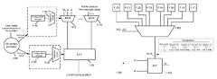
- FIG. 1illustrates a configurable IC of some embodiments in which each four tiles share one carry logic circuit.
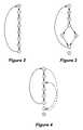
- FIG. 2illustrates several configuration data sets received by a reconfigurable circuit in a loop.
- FIG. 3illustrates an example of a reconfigurable circuit that conditionally transitions through configuration data sets.
- FIG. 4another example of a reconfigurable circuit that conditionally transitions through configuration data sets.
- FIG. 5another example of a reconfigurable circuit that conditionally transitions through configuration data sets.
- FIG. 6conceptually illustrates a time multiplexer in some embodiments.
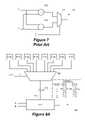
- FIG. 7illustrates a prior art circuit that conditionally performs either an add operation or a subtract operation.
- FIG. 8Aconceptually illustrates a circuit that conditionally performs either an add operation or a subtract operation in some embodiments.
- FIG. 8Bconceptually illustrates a multi-tier multiplexer of some embodiments that is utilized to supply configuration data to a configurable circuit.
- FIG. 9summarizes the actions that are taken to perform multiplication based on the value of the current three bits of the multiplier using a modified Booth algorithm.
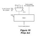
- FIG. 10conceptually illustrates a traditional implementation of a modified Booth multiplier that multiplies a multiplicand A, by a multiplier B.
- FIG. 11conceptually illustrates a modified Booth multiplier implemented using time multiplexer in some embodiments.
- FIG. 12is a prior art illustration of the operations that are required for performing MD5 encryption.
- FIG. 13conceptually illustrates an implementation of MD5 encryption in some embodiments utilizing time multiplexer.
- FIG. 14illustrates a circuit that produces an output in some embodiments.
- FIG. 15illustrates a circuit that implements an equivalent functionality as the circuit of FIG. 14 by using resource sharing.
- FIG. 16illustrates a circuit that produces an output in some embodiments.
- FIG. 17illustrates a circuit that implements an equivalent functionality as the circuit in FIG. 16 by using time multiplexer.
- FIG. 18illustrates Shannon decomposition used to break a function into two functions with fewer inputs.
- FIG. 19illustrates the use of time multiplexer in some embodiments to implement a 4-input function by utilizing a 3-input LUT.
- FIG. 20illustrates a process of some embodiments that uses Shannon decomposition to decompose a function that has more than a particular number of inputs.
- FIG. 21conceptually illustrates two input signals of a logic circuit that go through several other logic circuits prior to arrival.
- FIG. 22conceptually illustrates the arrival time of a set of inputs that are received by a circuit.
- FIG. 23illustrates a process of some embodiments that uses Shannon decomposition to decompose a 4-input function and implement the resulting two functions using time multiplexer.
- FIG. 24conceptually illustrates a tile of some embodiments.
- FIG. 25conceptually illustrates a tile of some embodiments.
- FIG. 26illustrates a space-time context generator of some embodiments.
- FIG. 27illustrates the timing between the Clk signal and the two sets of four one-hot signals.
- FIG. 28illustrates a space-time context generator of some embodiments that uses a user-design signal to generate the next space-time context.
- FIG. 29illustrates the detailed tile arrangement of some embodiments.
- FIG. 30illustrates a portion of a configurable IC of some embodiments of the invention.
- FIG. 31illustrates a more detailed example of data between a configurable node and a configurable circuit arrangement that includes configuration data that configure the nodes to perform particular operations.
- FIG. 32illustrates a system on chip (“SoC”) implementation of a configurable IC.
- SoCsystem on chip
- FIG. 33illustrates an embodiment that employs a system in package (“SiP”) implementation for a configurable IC.
- SiPsystem in package
- FIG. 34conceptually illustrates a more detailed example of an electronics system that has an IC, which implements inventions of some embodiments.
- Some embodimentsprovide a reconfigurable IC with at least one reconfigurable circuit that conditionally transitions through configuration data sets.
- the reconfigurable circuittransitions through configuration data sets based on a user-design signal.
- at least one reconfigurable circuitconditionally performs different operations on the same set of inputs.
- Some embodimentsprovide a method of operating a configurable circuit of an integrated circuit (IC).
- the methodperforms a first operation by the configurable circuit based on a first configuration data set.
- the methodgenerates a user-design signal within the IC.
- the methodperforms a second operation by the configurable circuit based on a second configuration data set, after the first operation.
- the methodperforms a third operation by the configurable circuit based on a third configuration data set, after the first operation.
- the first, second, and third configuration data setsare supplied to the configurable circuit by a selection circuit that receives a selection signal based on the user-design signal.
- the selection signalis generated by a signal generator that receives the user-design signal and generates the selection signal based on the user-design signal.
- the user-design signalis a non-repetitive, non-clock signal.
- a reconfigurable integrated circuitthat includes a set of reconfigurable circuits and sets of configuration storage elements.
- Each set of configuration storage elementsis associated with one reconfigurable circuit.
- Each set of configuration storage elementsstores several configuration data sets.
- Each configuration data setdefines a set of operations that a reconfigurable circuit performs.
- At least one reconfigurable circuitreceives a first sub-set of its configuration data when a user-design signal has a first value and receives a second sub-set of its configuration data when the user-design signal has a second value.
- the reconfigurable ICalso includes a set of selection circuits.
- Each selection circuitcan supply several configuration data sets from the configuration storage elements to each reconfigurable circuit.
- At least one selection circuitconditionally supplies configuration data sets to the at least one reconfigurable circuit based on the user-design signal.
- Some embodimentsprovide a method of performing a mathematical operation on a set of operands.
- the mathematical operationincludes several sub-operations.
- the methodexamines several bits of at least one operand at a time and depending on the value of these bits, reconfigures a single logic circuit to perform one of the sub-operations to generate a partial result of the mathematical operation.
- the logic circuitis reconfigured by receiving a first set of configuration data that cause the logic circuit to reconfigure to perform a first sub-operation operation and a second set of configuration data that cause the logic circuit to reconfigure to perform a second sub-operation.
- the logic circuitreceives different inputs based on the value of the bits being examined.
- the mathematical operationis multiplication and the sub-operations are addition and subtraction.
- Some embodimentsprovide a reconfigurable integrated circuit (“IC”) that can perform multiplication.
- the ICincludes a first reconfigurable logic circuit and a signal generator that can generate a selection signal based on a value of a particular number of bits of a multiplier.
- the ICalso includes a first selection circuit that ca supply several configuration data sets for the first reconfigurable circuit based on the selection signal.
- the reconfigurable logic circuitis reconfigured to perform either an addition operation or a subtraction operation to generate a partial result of the multiplication.
- the ICalso includes a second reconfigurable circuit that can supply several inputs to the first configurable circuits and a second selection circuit that can supply several configuration data sets for the second reconfigurable circuit based on the selection signal. Based on the selection signal, the second reconfigurable circuit supplies either a value of a multiplicand, twice the value of the multiplicand, or a value of 0 as input to the first reconfigurable circuit.
- Some embodimentsprovide a method of performing circuit synthesis that receives a design that has a function with several inputs.
- the methodidentifies a set of early arriving inputs of the function and performs Shannon decomposition on the function based on one of the early arriving inputs.
- the methodestimates the number of circuits a signal has to travel through to reach each input of the function and selects a set of inputs with signals that travel through fewer numbers of circuits compared to signals of inputs that are not selected.
- the methodrecursively identifies early arriving signals and performs Shannon decomposition on the resulting functions until Shannon decomposition results in a set of functions all of which with fewer than a particular number of inputs.
- Some embodimentsprovide a computer readable medium that stores a computer program that can perform circuit synthesis.
- the computer programis executable by at least one processor.
- the computer programincludes sets of instructions for receiving a design comprising a function with a plurality of inputs, for identifying a set of early arriving inputs of the function, and for performing a function decomposition on the function based on one of the early arriving inputs.
- Section IIdescribes a discussion of the configurable IC architecture that is used by some of these embodiments. This discussion is followed by the discussion in Section III of reconfigurable circuits that loop through less than the maximum number of available configuration data sets.
- Section IVdescribes time multiplexers and discusses how portions of the IC in some embodiments go through sub-cycle configuration conditionally.
- Section Vdescribes the use of time multiplexers and function decomposition in automatic circuit design.
- Section VIdescribes the space-time context generator of some embodiments that generates sub-cycle signals to drive a reconfigurable circuit to go through the states in a loop.
- Section VIIdescribes a configurable IC and an electronics system that has an IC which implements some of the embodiments of the invention.
- a reconfigurable ICis a form of a configurable IC.
- a configurable circuitis a circuit that can “configurably” perform a set of operations. Specifically, a configurable circuit receives “configuration data” that specifies the operation that the configurable circuit has to perform from the set of operations that it can perform. In some embodiments, the configuration data is generated outside of the configurable IC.
- a set of software toolstypically converts a high-level IC design description (e.g., a circuit representation or a hardware description language design) into a set of configuration data that can configure the configurable IC (or more accurately, the configurable circuits of the configurable IC) to implement the IC design.
- a reconfigurable ICis a configurable IC that has at least one circuit that reconfigures during runtime.
- a reconfigurable ICis an IC that has reconfigurable logic circuits and/or reconfigurable interconnect circuits, where the reconfigurable logic and/or interconnect circuits are configurable logic and/or interconnect circuits that can “reconfigure” more than once at runtime.
- a configurable logic or interconnect circuitreconfigures when it receives a different set of configuration data.
- Some embodiments of the inventionare implemented in reconfigurable ICs that are sub-cycle reconfigurable (i.e., can reconfigure circuits on a sub-cycle basis).
- a reconfigurable IChas a large number of logic and interconnect circuits (e.g., hundreds, thousands, etc. of such circuits). Some or all of these circuits can be reconfigurable.
- runtime reconfigurabilitymeans reconfiguring without resetting the reconfigurable IC.
- Resetting a reconfigurable ICentails in some cases resetting the values stored in the state elements of the IC, where state elements are elements like latches, registers, and non-configuration memories (e.g., memories that store the user signals as opposed to the memories that store the configuration data of the configurable circuits).
- runtime reconfigurabilitymeans reconfiguring after the reconfigurable IC has started processing of the user data.
- runtime reconfigurabilitymeans reconfiguring after the reconfigurable IC has powered up.
- FIG. 1conceptually illustrates a portion 100 of the configurable circuit architecture of some embodiments of the invention. As shown in FIG. 1 , this architecture is formed by numerous conceptual configurable tiles 105 that are arranged in an array with multiple rows and columns.
- each configurable tileis a conceptual grouping of a configurable three-input logic circuit 110 , three configurable input-select interconnect circuits 115 , and several configurable routing interconnect circuits 120 . Different embodiments have different number of configurable routing interconnect circuits 120 . For instance, some embodiments may have eight configurable routing interconnect circuits while others may have more or less such circuits.
- the configurable ICincludes a set of storage elements (not shown) for storing a set of configuration data.
- the logic circuitsare look-up tables (LUTs) while the interconnect circuits are multiplexers.
- the LUTs and the multiplexersare sub-cycle reconfigurable circuits, as described in U.S. patent application “Configurable IC with Routing Circuits with Offset Connections”, Ser. No. 11/082,193, filed on Mar. 15, 2005.
- the configurable ICstores multiple sets of configuration data for a sub-cycle reconfigurable circuit, so that the reconfigurable circuit can use a different set of configuration data in different sub-cycles.
- Other configurable tilescan include other types of circuits, such as memory arrays instead of logic circuits.
- an input-select multiplexer 115is an interconnect circuit associated with the LUT 110 that is in the same tile as the input select multiplexer.
- One such input select multiplexerreceives input signals for its associated LUT and passes one of these input signals to its associated LUT.
- a routing multiplexer 120is an interconnect circuit that at a macro level connects other logic and/or interconnect circuits.
- a routing multiplexereither provides its output to several logic and/or interconnect circuits (i.e., has a fan out greater than 1), or provides its output to other interconnect circuits.
- an RMUXis a complementary pass logic (CPL) implemented 8-to-1 multiplexer.
- an RMUXmay have a latch built in its output stage.
- a complementary pair of signalsrepresents each logic signal.
- the circuitreceives true and complement sets of input signals and provides true and complement sets of output signals.
- the two (true and complement) outputs of the 8-to-1 multiplexercan be cross coupled with two NMOS transistors that receive a latch enable signal at their gates.
- each tileincludes one three-input LUT, three input select multiplexer and several routing multiplexers.
- every four tiles 125share a carry logic circuit 130 .
- the term 4-aligned LUT tilerefers to four tiles (each with one LUT) with a common carry logic circuit.
- HMUXhybrid multiplexers
- An HMUXis a multiplexer that can receive “user-design signals” or configuration data.
- a user-design signal within a configurable ICis a signal that is generated by a circuit (e.g., logic circuit) of the configurable IC.
- the word “user” in the term “user-design signal”connotes that the signal is a signal that the configurable IC generates for a particular application that a particular user has configured the IC for.
- User-design signalis abbreviated to user signal in some of the discussions below.
- a user signalis a signal that is generated within the configurable IC.
- a user signalis a signal that is a function of at least a portion of the configuration data received by the configurable IC and at least a portion of the inputs to the configurable IC.
- the user signalcan also be dependent on (i.e., can also be a function of) the state of the configurable IC.
- the initial state of a configurable ICis a function of the configuration data received by the configurable IC and the inputs to the configurable IC.
- Subsequent states of the configurable ICare functions of the configuration data received by the configurable IC, the inputs to the configurable IC, and the prior states of the configurable IC.
- a configurable ICWhen implementing a particular user design, a configurable IC performs user-design operations that allow the IC to implement the particular user design in a circuit or device. During such user-design operations, the configurable IC (1) can receive user-design input data, which are neither configuration signals nor clocking signals, and (2) can process these signals to implement the particular user design in a circuit or device. Accordingly, in some cases, a configurable IC performs user-design operations when it receives and processes user-design input data and provides user design output data. For instance, when the configurable IC performs user-design operations, its configurable logic circuits in some cases can receive user-design input data, compute functions based on the user-design input data, and output their results to other circuits inside the IC. In other contexts, a configurable IC might implement a user design that simply directs the IC to generate output without receiving any user-design input.
- clocking signalsWhen a configurable IC performs user-design operations, its circuits typically receive clocking signals that allow them to process user-design signals. Examples of such clocking signals include (1) clocking signals applied to input/output buffer circuits that allow these circuits to receive and output user-design data, (2) clocking signals applied to the configurable logic circuits that allow these circuits to compute user-design functions, and/or (3) clocking signals applied to the IC's configurable interconnect circuits that allow these circuits to perform user-design connection operations. In case of a reconfigurable IC that has reconfigurable circuits that receive different configuration data sets loaded on the IC, the clock signals can also include clock signals that allow the reconfigurable circuit to step through the different configuration data sets.
- a reconfigurable circuitreceives configuration data sets sequentially in an order that loops from the last configuration data set to the first configuration data set.
- FIG. 2illustrates eight configuration data sets received by a reconfigurable circuit according to such a looping sequence that can loop through configuration data sets. In this figure, the arrows illustrate how the configuration data sets follow each other.
- Such a sequential reconfiguration schemeis hereinafter referred to as a “loopered” scheme.
- FIG. 2illustrates an 8-loopered scheme for providing the configuration data sets to a reconfigurable circuit. The full cycle of the reconfigurable circuit is, therefore, divided into eight sub-cycles.
- each one of the eight configuration data sets ( 0 - 7 )provides a space-time context (or configuration state) for the reconfigurable circuit.
- Each space-time contextis defined by a set of bits.
- the space-time context for a reconfigurable circuit in a particular clock cycle or sub-cycleis the configuration data sets that the circuit receives during the cycle.
- Each set (or word) of configuration datais termed as context as it defines the operation (i.e., the logic or interconnect operation) that a particular reconfigurable circuit (i.e., a logic circuit or an interconnect circuit) performs for a particular cycle out of the rest of operations that the circuit can perform.
- space-time context for the ICis all the configuration data sets that all the reconfigurable circuits receive during that cycle.
- a reconfigurable circuitdoes not receive all configuration data sets in each loop. This is the case when, e.g., due to timing constraints, a portion of the user design does not require all configuration data sets to run.
- the unused configuration data setscan be utilized to conditionally perform different operations. For instance, if there are n configuration data sets, a reconfigurable circuit may conditionally cycle through m (where m is smaller than n) configuration states in each loop based on a certain condition.
- FIG. 3illustrates one such example. Specifically, it illustrates eight configuration data sets that are available for a particular reconfigurable circuit.
- the circuitreceives either configuration data set 1 or configuration data set 3 . Specifically, as long as a certain condition (such as presence of a certain signal) is true, then the reconfigurable circuit receives configuration data sets 0 , 1 , 2 , 5 , 6 , and 7 in a loop. Once the condition becomes false, the circuit receives configuration data sets 0 , 3 , 2 , 5 , 6 , and 7 in a loop. As shown, configuration data set 4 is not used for the particular reconfigurable circuit and the particular user design shown in FIG. 3 . A full cycle of the reconfigurable circuit that receives the configuration data sets shown in FIG. 3 is, therefore, divided into 6 sub-cycles. In some embodiments, a user-design signal determines the condition upon which the reconfigurable circuit receives a particular configuration data set.
- FIG. 4illustrates eight configuration data sets 0 - 7 .
- the reconfigurable circuitreceives either configuration data sets 0 , 1 , 2 , 5 , 6 , and 7 or configuration data sets 0 , 3 , 2 , 5 , 6 , and 7 .
- configuration data set 4is not used for the particular reconfigurable circuit and the particular user design shown in FIG. 4 .
- a full cycle of the reconfigurable circuit that receives the configuration data sets shown in FIG. 4is, therefore, divided into 6 sub-cycles.
- FIG. 5illustrates another possible way of conditionally going through eight possible configuration data sets.
- the reconfigurable circuitreceives either configuration data sets 0 , 5 , 2 , 7 or 4 , 1 , 6 , 3 .
- the reconfigurable circuitmay receive configuration data set 4 instead of configuration data set 0 .
- the reconfigurable circuitmay receive configuration data set 0 instead of configuration data set 4 .
- the decision to which configuration data set the circuit receivesdepends on the value of a user signal (not shown). For instance, as will be described below, in FIG. 3 a particular user signal with a value of 0 may cause the reconfigurable circuit to receive configuration data set 1 after configuration data set 0 .
- the configuration data set 1may, for instance, reconfigure the circuit to perform an add operation.
- a value of 1 for that user signalmay cause the reconfigurable circuit to receive configuration data set 3 after configuration data set 0 and reconfigure to perform a subtraction operation.
- Time multiplexerconceptually refers to configurable circuits conditionally going through their configuration data sets.
- some embodimentsuse space-time context generators (ST-context generators) which generate sub-cycle signals that control the operations of the circuitry that provides configuration data sets to the configurable circuits.
- ST-context generatorsalso referred to as sub-cycle signal generators
- receive user signalswhich cause them to modify the signals it generates for different configurable circuits.
- these users design signalscause the configurable circuits to conditionally transition through their configuration data sets by having the ST-context generator to modify its output which in turn modify the configuration data fetching circuitry associated with the configuration circuits.
- a TMUXprovides the ability to make configuration decisions based on user signals.
- a TMUXis conceptually illustrated in FIG. 6 .
- the ST-context generator 615operates as a counter that decodes the next row of configuration storage 610 .
- the ST-context generatorreceives a set of configuration bits 620 that determine whether the ST-context generator operators, e.g., in any of the 2, 4, 6, or 8 loopered configurations.
- a user signal 605determines the next row of the configuration storage 610 that is decoded.
- the configuration storagestores a set of configuration data bits for a configurable circuit.
- a selection circuit 625supplies the configuration data sets to a reconfigurable circuit (not shown).
- a TMUXre-coups the waste of configuration storage when, due to timing constraints, a user design is not run at the highest looperedness (i.e., the user design is not using all configuration data sets in each particular loop).
- this configuration storagecan be reused. What differentiates the techniques is whether the user specifies the “decision” to be made by the TMUX, or whether the synthesis tools determine it directly from a user register transfer level (RTL) description of the user design.
- RTLuser register transfer level
- An example of a user determined decisionis two substantial design modules which are mutually exclusive. Which of the two modules is currently relevant is determined by the state of the design. The two modules can be placed on the same region and the TMUX can be used to select between these two contexts based on the design state. In the case of tools doing the determination, the tools can do “Shannon decomposition in time” to determine two mutually exclusive configuration of a logic circuit based on previously known logic values.
- the extra configuration data set(s)can be utilized to conditionally perform different operations in that particular part of the design.
- FIG. 7illustrates a prior art circuit 700 that conditionally performs either an add operation or a subtract operation.
- the two inputs, X and Y,are fed to the adder 705 and the subtractor 710 .
- the outputs of the adder 705 and the subtractor 710are connected to the inputs of the 2-to-1 multiplexer 715 .
- a signal, Z, that is connected to select line of multiplexer 715determines the results of which of the two operations is output from the multiplexer.
- FIG. 8Aconceptually illustrates a circuit 800 that conditionally performs an add operation or a subtract operation in some embodiments.
- the 8-to-1 multiplexerreceives eight sets of configuration data, F( 0 ) to F( 7 ), at its inputs.
- Each set of configuration data, F( 0 ) to F( 7 )is a multi-bit value.
- the multiplexerBased on the value of the multi-bit select signal S, the multiplexer connects one of its inputs to its output.
- the signal Sis dependent on the value of a user signal, Z.
- the output of the multiplexer 805is connected to the input of the look-up table (LUT) 810 .
- LUT 810is a reconfigurable circuit.
- the configuration data set 815 that the LUT receivesdetermines the operation that the LUT performs during that sub-cycle.
- the 8-to-1 multiplexeris implemented as a two-tiered multiplexer.
- FIG. 8Bconceptually illustrates such a two-tiered multiplexer 820 .
- the first tierhas two 4-to-1 multiplexers 825 and 830
- the second tierhas one 2-to-1 multiplexer 835 .
- the multiplexers in the first tierreceive configuration data as their inputs. Specifically, multiplexer 825 receives F( 0 ), F( 2 ), F( 4 ), and F( 6 ) while multiplexer 830 receives F( 1 ), F( 3 ), F( 5 ), and F( 7 ) at their inputs.
- Two bits (S 1 and S 2 ) of the select signal Scontrol the multiplexers of the first tier and one bit (S 3 ) controls the multiplexer of the second tier.
- one of the configuration bits F( 0 ) to F( 7 )is selected to connect to the output of the two-tiered multiplexer 820 .
- Some embodiments that use this two-tiered structurebuild the first tier of multiplexers into the sensing circuitry of the configuration storage. Examples of this structure are described in the above mentioned U.S. application Ser. No. 11/081,859.
- the 3-bit select signal S of the multiplexer 805selects configuration data sets F( 0 ), F( 1 ), F( 2 ), F( 5 ), F( 6 ), and F( 7 ).
- the select signal S of the multiplexerselects configuration data sets F( 0 ), F( 3 ), F ( 2 ), F( 5 ), F( 6 ), and F( 7 ).
- the LUTis designed to perform an add operation if it receives configuration data set F( 1 ) and to perform a subtract operation if it receives configuration data set F( 2 ). The LUT, therefore, conditionally performs either an add or a subtract operation based on the value of the user signal, Z.
- Circuit 800performs a similar operation as circuit 700 . While circuit 700 requires an adder ( 705 ), a subtractor ( 710 ), and a multiplexer ( 715 ), circuit 800 only needs a LUT and its associated configuration multiplexer 805 . Circuit 800 , therefore, saves on the logic circuitry and routing resources.
- the following exampleshows how a modified Booth recoding scheme is implemented using the time-space context generator in some embodiments to perform multiplication.
- a Booth multipliertwo bits of the multiplier are considered at a time and a partial product (which is initially set to 0) is updated based on the value of the current two bits of the multiplier.
- the Booth algorithmexploits the equality, (A), to create faster multipliers by replacing a sequence of n 1s in the multiplier (that requires n additions), by one addition and one subtraction.
- the Booth algorithmdoesn't perform well when the multiplier has a singleton 1 (i.e., a 1 separated by 0s) which would replace one addition by one addition and one subtraction.
- the modified Booth algorithmis an improvement of the Booth algorithm.
- Table 900 in FIG. 9summarizes the actions that are taken by the modified Booth multiplier algorithm to perform multiplication based on the value of the current three bits of the multiplier.
- the modified Booth multiplier algorithmignores runs of 0 or 1 in the multiplier. Therefore, as shown in Table 900 , when the three bits of the multiplier are 000 or 111, no action is required.
- a singleton 1 (010)requires the multiplicand to be added to the partial result.
- a single 1 at the end of a run of 1 (001) and two is at the end of a run of 1 (011)require adding either the multiplicand or two times the multiplicand to be added to the partial result, respectively.
- a single 1 beginning a run of is (001) or two is beginning a run of is (110)require subtracting two times the multiplicand or the multiplicand from the partial results, respectively.
- end of run of 1s and beginning of another (101)requires subtracting the multiplicand from the partial results.
- FIG. 10conceptually illustrates a traditional implementation of the modified Booth multiplier that multiplies a multiplicand A, by a multiplier B.
- the partial productis initially set to zero (not shown).
- the bits of the multiplierare examined three at a time.
- the current three bits of the multiplierare utilized as the three select lines of multiplexer 1010 .
- the values of the current three bits of the multiplier(B i , B i ⁇ 1 , and B i ⁇ 2 ) determine what value is added to the partial product.
- Table 900shows the required action for each combination of 000 to 111 of the current three bits of the multiplier.
- FIG. 11conceptually illustrates a Booth multiplier implemented using TMUX.
- ST-context generator 1120uses the user signal (which is the current three bits of the multiplier) to generate space-time context for each sub-cycle.
- the context generator 1120does not make context generation in a traditional sense, instead it operates as a per sub-cycle multiplier function. Specifically, instead of cycling through as a counter, it uses the three current bits of the multiplier to generate the sub-cycle signal.
- LUT 1105is a reconfigurable circuit and can reconfigure to perform either addition or subtraction. As shown, LUT 1105 has an associated selection circuit 1125 and configuration storage 1130 that receive the sub-cycle signal from the ST-context generator and supply space-time context to the LUT.
- IMUXs 1110 and 1115route inputs to the LUT.
- IMUX 1110has an associated selection circuit 1135 and configuration storage 1140 that receive the sub-cycle signal from the ST-context generator and supply space-time context to the LUT.
- IMUX 1110also has an associated selection circuit and configuration storage which are not shown in FIG. 11 . Since LUT 1105 is a reconfigurable circuit, instead of adding ⁇ or 2A the value of A or 2A is subtracted from the partial product, respectively. This reduces the inputs of the IMUX 1110 by two and saves routing resources.
- IMUX 1110is used to input the next values to add or subtract.
- IMUX 1115is used to input the partial product from the previous sub-cycle.
- ST-context generator 1120In each sub-cycle, depending on the values of the current three bits of the multiplier, ST-context generator 1120 generates an appropriate signal to selection circuit 1125 and configuration storage 1130 which causes them to supply the appropriate configuration data to LUT 1105 to configure the LUT as either an adder or a subtractor.
- LUT 1105is either configured to act as an adder (when the current three bits of the multiplier are 000, 001, 010, 011, and 111) or as a subtractor (when the bits are 100, 101, or 110).
- IMUX 1110is configured to input either 0 (when the current three bits of the multiplier are 000 or 111), A (when the bits are 001 or 010, 101, or 110), or 2A (when the bits are 011 or 100) to LUT 1110 . Some embodiments require only the two values of A and 2A (and not the value of 0) to be input to IMUX 1110 . In these embodiments, LUT 1105 is configured to leave the partial product unchanged when the three bits of the multiplier are 000 or 111.
- MD5 encryption operationsare a set of AND, OR, and exclusive OR (XOR) operations that are performed on two inputs.
- FIG. 12conceptually illustrates operations that are required for performing MD5 encryption on a set of two 32-bit values, A and B.
- the multiplexer 1205selects one of the outputs of function generators 1210 - 1225 .
- Function generators 1210 - 1225perform A ⁇ B, ⁇ B, A+ B , and A ⁇ B operations respectively.
- implementing a circuit 1200 to perform MD5 encryptionrequires many routing resources. Specifically, the 32-bit inputs, A and B, have to be routed to function generators 1210 - 1225 and the 32-bit outputs of these function generators have to be routed to the inputs of multiplexer 1205 .
- FIG. 13conceptually illustrates a circuit 1300 that performs MD5 encryptions in some embodiments.
- the 8-to-1 multiplexer 1305receives eight sets of configuration data, F( 0 ) to F( 7 ), at its inputs. Based on the value of the select signal S, the multiplexer connects one of its inputs to its output. The signal S is dependent on the values of user signals, Z 1 and Z 2 . As shown, the output of multiplexer 1305 is connected to the input of the look-up table (LUT) 1310 .
- LUT 1310is a reconfigurable circuit. In each sub-cycle, the configuration data set 1315 that the LUT receives determines the operation that the LUT performs during that sub-cycle.
- the multiplexerselects configuration data sets F( 1 ) and F( 2 ).
- the multiplexerselects configuration data sets F( 1 ) and F( 4 ).
- the multiplexerselects configuration data sets F( 1 ) and F( 6 ).
- the multiplexerselects configuration data sets F( 1 ) and F( 8 ).
- the LUTis designed to perform an XOR operation when it receives configuration data set F( 2 ), to perform AND operation between B and the complement of A when it receives configuration data set F( 4 ), to perform OR operation between A and the complement of B when it receives configuration data sets F( 6 ), and to perform AND operation when it receives configuration data set F( 8 ).
- the LUTtherefore, conditionally performs the operations that are required for MD5 encryption based on the value of the user signals, Z 1 and Z 2 .
- circuit 1300requires that the two 32-bit inputs, A and B to be routed to the inputs of only one logic circuit, i.e., LUT 1310 . Therefore, comparing with the prior art arrangement shown in FIG. 12 , circuit 1300 saves a large amount of routing resources. In addition, circuit 1300 requires only one function generator (e.g., LUT 1310 ) as oppose to the four function generators 1210 - 1225 required in FIG. 12 . Therefore, comparing with the prior art, circuit 1300 also saves on the computing resources.
- LUT 1310function generator
- FIG. 14illustrates a circuit 1400 that conditionally performs an add operation on either of two sets of inputs (A and B or C and D) and produces an output 1420 .
- the inputs to multiplexer 1415are the outputs of adder 1405 (i.e., A+B) and the output of adder 1410 (C+D).
- adder 1405i.e., A+B
- adder 1410C+D
- multiplexer 1415selects the output of either adder 1405 or 1410 to connect to the output 1420 .
- circuit 1400performs the same operation (i.e., addition) on different sets of inputs (either A and B or C and D) to produce mutually exclusive results (multiplexer 1415 only allows the output of one of the adders 1405 and 1410 to appear at the output 1420 ).
- FIG. 15illustrates a circuit 1500 that has an adder 1515 and two multiplexers 1505 and 1510 .
- the two multiplexershave the same select signal, S.
- Sselect signal
- the input to the adderare, therefore, either A and B or C and D.
- the output 1520 of the circuit 1500is either A+B or C+D.
- Circuit 1500implements the same functionality as circuit 1400 by sharing the adder resource to generate two mutually exclusive results. Note that if the logic circuit (in this case adder 1515 ) can perform other similar operations, such as subtraction, resource sharing can be utilized to perform similar operations. There is, however, the limitation that the operations have to be performed by the same logic unit that is being shared and the outputs should not be needed at the same time.
- TMUXUtilizing TMUX is a more generalized way of utilizing the resources.
- the only requirement to use TMUXis to have functions that operate conditionally to produce mutually exclusive outputs. In other words, using TMUX does not require the operations to be performed by the same logic unit nor the input sets need to be necessarily different.
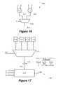
- FIG. 16illustrates a circuit 1600 that produces an output 1620 .
- the inputs to multiplexer 1615are the outputs of the logic circuit 1605 (i.e., A XOR B) and the output of the logic circuit 1610 (C+D).
- multiplexer 1615selects the output of either the logic circuit 1605 or 1610 to connect to the output 1620 . Since the two logic circuits 1605 and 1610 perform different operations (i.e., XOR and addition), resource sharing technique shown in FIG. 15 cannot be used to implement an equivalent for circuit 1600 .
- An equivalent of circuit 1600can be implemented using TMUX.
- FIG. 17illustrates a circuit 1700 that conditionally performs either an add operation or an XOR operation and produces an output 1720 .
- the 4-to-1 multiplexer 1705receives four sets of configuration data, F( 0 ) to F( 3 ), at its inputs. Based on the value of the select signal S, the multiplexer connects one of its inputs to its output. The signal S is dependent on the value of a user signal, Z. As shown, the output of the multiplexer 1705 is connected to the input of the look-up table (LUT) 1710 .
- LUT 1710is a reconfigurable circuit. In each sub-cycle, the configuration data set 1715 that the LUT receives determines the operation that the LUT performs during that sub-cycle.
- the select signal S of the multiplexerselects configuration data sets F( 0 ) and F( 1 ).
- the multiplexerselects configuration data sets F( 0 ) and F( 3 ).
- the LUTis designed to perform an XOR operation if it receives configuration data set F( 1 ) and to perform an addition operation if it receives configuration data set F( 3 ). The LUT, therefore, conditionally performs either an XOR or an addition operation based on the value of the user signal Z received at the select line S.
- Circuit 1700performs a similar operation as the circuit 1600 . While the circuit 1600 requires two logic circuits 1605 and 1610 and a multiplexer 1615 , circuit 1700 only needs a LUT and its associated configuration multiplexer 1705 . Circuit 1700 , therefore, saves on the logic circuitry and routing resources in a situation where two different operations have to be performed.
- TMUXscan be used to implement functions with large fan-ins using circuit components with fewer inputs. More specifically, some embodiments use a function decomposition (e.g., Shannon decomposition) to decompose functions.
- a Shannon decompositiondecomposes a function F(a, b, . . . , n) into two functions F 0 and F 1 , each with one less input.
- Some embodimentsuse TMUXs to implement the “if-then-else” (ITE) expression needed for Shannon decomposition. For instance, if the user design requires only four space-time contexts and the space-time context generator supports generating eight configuration data sets, the extra space-time context can be used to perform a function that is decomposed using Shannon decomposition.
- ITEif-then-else
- the reconfigurable circuitscan be programmed to use one set of the space-time context (e.g., space-time context 0) if the user input (e.g., variable a in Equation A, above) is 1 and to use the other set of space-time context (e.g., space-time context 2) if the user input is 0.
- the reconfigurable circuitsare then designed in a way that when they receive the space-time context 0, they perform the first part of the Shannon decomposed function (e.g., F 1 (b, . . . , n) in Equation A, above) and when they receive the space-time context 2, they perform the other part of the Shannon decomposed function (e.g., F 0 (b, . . . , n) in Equation A, above).
- FIG. 18illustrates a function, G that requires four inputs a, b, c, and d.
- Shannon decompositionis used to break this function into two functions with three inputs each.
- the four input function G(a, b, . . . , n)is decomposed into two functions G 0 and G 1 :
- G ( a,b,c,d )[ ⁇ a ⁇ G 1 ( b,c,d ) ⁇ + ⁇ ⁇ G 0 ( b,c,d ) ⁇ ]
- function Gis implemented with two 3-input logic circuits 1805 and 1810 as well as two AND gates and one OR gate.
- FIG. 18illustrates a function, G that requires four inputs a, b, c, and d.
- Shannon decompositionis used to break this function into two functions with three inputs each.
- the four input function G(a, b, . . . , n)is decomposed into two functions G 0 and G
- Multiplexer 1905is designed to provide configuration data sets 1915 to logic circuit (in this example, a LUT) 1910 . Depending on the value of its select signal, S, multiplexer 1905 connects one of two groups of configuration data sets to LUT 1910 . As shown, the select signal is a function of input “a” of function G. If a is 0, the group F( 1 ), F( 2 ), F( 3 ), F( 4 ), F( 5 ), and F( 6 ) is used in a loop to configure the LUT.
- the group F( 1 ), F( 0 ), F( 3 ), F( 4 ), F( 5 ), and F( 6 )is used in a loop to configure the LUT.
- LUT 1910By configuring LUT 1910 to perform function G 0 when the LUT receives configuration data set F( 2 ) and to perform function G 1 when the LUT receives configuration data set F( 0 ), the 3-input LUT 1910 can perform 4-input function G.
- FIG. 20illustrates a process 2000 of some embodiments that uses Shannon decomposition to decompose a function that has more than a particular number of inputs. For instance, in some embodiment if a certain portion of an IC has circuits to perform 3-input functions, the particular number of inputs is set to four. The resulting functions are decomposed using Shannon decomposition one more time as described further below in connection with FIG. 23 before being implemented.
- the processreceives (at 2005 ) the function to decompose.
- the processdetermines (at 2010 ) whether the function has more than a particular number of inputs. If no, the process exits. Otherwise, the process proceeds to 2015 to compute the estimated arrival time of each input of the function.
- the processselects (at 2020 ) one of the inputs as the pivot to perform Shannon decomposition.
- This inputwill be used, as input “a” is used in equation (B) above, to decompose the received function.
- one of the earliest arriving inputis selected to perform the decomposition.
- An early arriving signalis used to ensure that the input signal that is used in selecting configuration bits arrives early and is stable at the beginning of the sub-cycle.
- the use of an early arriving signal for doing Shannon decomposition in this inventionis in contrast to the use of late arriving signals that is common with doing Shannon decomposition in circuit design. Prior use of Shannon decomposition in circuit design used the late arriving signals in doing the decomposition in order to allow operations be done on the early arriving signals selected with the late arriving signal.
- the early arriving input signalsare estimated by the number of logic circuits the signal has to travel through to arrive at the input. For instance, as shown in FIG. 21 the signal for input “a” of the logic circuit 2105 has to go through four logic circuits 2110 - 2125 while the input signal for the input “d” has to go through only two logic circuits 2130 - 2135 . The signal for “d” input which goes through less number of circuits is, therefore, estimated to arrive earlier than the signal for input “a”.
- a heuristicis used to select one of the earliest arriving inputs to perform Shannon decomposition.
- the selected input(not necessarily the particular earliest arriving input) is chosen from a group of inputs that, when used as the pivot in Shannon decomposition, will not cause any delays in generating the final result of the received function.
- FIG. 22conceptually illustrates a set of inputs i 1 to i n , that are received by a circuit. Some embodiments identify a group of early arriving signals 2205 . For instance, in some embodiments these inputs have to arrive before a threshold time 2210 .
- this threshold timeis a certain amount time (shown by time period 2215 ) prior to an event 2220 .
- this event 2220is the time that the circuit produces an output for the current user clock cycle. In other embodiments, this event is the start of the next user clock cycle. In some embodiments, the time period 2215 is selected such that it allows for an arrived signal in input group 2205 to become stable for being used during the next user clock cycle.
- Different embodimentsuse different techniques to identify which input in the early arriving input group 2205 to be used as pivot for Shannon decomposition. Some embodiments perform trial and error to select one of the inputs. Some embodiments associate a cost (e.g., number of logic circuits, amount of required routing resources, delays produced in generating the output, etc.) for the decomposition and select an input that minimized the given cost.
- a coste.g., number of logic circuits, amount of required routing resources, delays produced in generating the output, etc.
- the processperforms (at 2025 ) Shannon decomposition on the received function based on the identified input.
- the processdetermines (at 2030 ) whether any resulting functions of Shannon decomposition has more than the particular number of inputs.
- the processproceeds to 2040 which is described below. Otherwise, the process recursively calls itself (at 2035 ) once for each of these functions.
- the processreturns (at 2040 ) the functions that the process identified itself or identified through its recursive calls, and then ends.
- FIG. 23illustrates a process 2300 that facilitates implementing a 4-input function using a 3-input reconfiguration circuit.
- FIG. 23illustrates a process 2300 that facilitates implementing a 4-input function using a 3-input reconfiguration circuit.
- this exampleis shown for a 4-input function, a person of ordinary skill in the art realizes that the same technique can be used to implement any n-input function with a reconfigurable circuit with n ⁇ 1 inputs.
- the processreceives (at 2305 ) the function to be implemented.
- the processthen computes (at 2310 ) the estimated arrival time of each of the input signals of the function.
- the processselects (at 2315 ) an input as pivot for Shannon decomposition as described in relation with process 2000 above.
- the processperforms (at 2320 ) Shannon decomposition on the function to extract this input.
- the processthen assigns (at 2325 ) the two resulting 3-input functions to two separate contexts of a function generator (such as a LUT), where each one of the contexts is selected in a particular sub-cycle based on the extracted signal.
- the IC synthesizerhas to designate an association between the two functions in order for the placer to assign both functions to the same LUT to ensure the correct operation of the resulting TMUX.
- some embodimentsuse a multi-tiered multiplexer structure that uses three clocks signals CLK, STo, and STe to select different configuration data sets for a configurable circuit.
- the configuration data setsthen determine the function that the configurable circuit performs.
- the configuration data sets for configurable circuitsare stored in memory locations (e.g., in SRAM cells), referred to as configuration storage. Examples of tiered multiplexer structures are described in detail in the above mentioned U.S. patent application Ser. No. 11/081,859.
- each one of the clock signals CLK, STo, and STeare generated as a differential pair of signals.
- Some of these embodimentsglobally distribute the differential pair of CLK and CLK signals, while locally generating the signals STo ⁇ 0:3> and STe ⁇ 0:3>.
- Some embodimentsuse a global clock generator to generate the differential clock signals CLK and CLK .
- the global clock generatoris outside of the configurable tile arrangement (e.g., the generator might be on a different circuit than the IC that includes the configurable tile arrangement, or it might be partially or completely on the IC that includes the arrangement but positioned outside of the arrangement). However, in other embodiments, this global clock generator can be placed within the configurable tile arrangement.
- the globally distributed differential clock signals CLK and CLKare received by two local ST-context generators in each tile.
- FIG. 24conceptually illustrates a tile 2400 of some embodiments.
- the local ST-context generator 2425 in the tileprovides the signals STo and STe for the tiered multiplexer structures that retrieve and provide configuration data sets to the routing multiplexers of the tile.
- the local ST-context generator 2420 in the tileprovides the signals STo and STe for the tiered multiplexer structures that retrieve and provide configuration data sets to the input select multiplexers and three-input LUT of the tile. Having two different local ST-context generators 2420 and 2425 for each tile allows the embodiments illustrated in FIG.
- routing multiplexers of a tileoperate on different clock domains than the input select multiplexers and the LUT of the tile. This is beneficial for allowing the routing multiplexers of a tile to be used to route signals that belong to different clock domains than the logic circuits of the tile.
- some embodimentsinclude one global clock generator for each clock domain that the reconfigurable IC can handle. For instance, an IC design might require the IC to interface with two bus interfaces that operate at two different rates and to implement a particular design that operates at yet another rate. In such a situation, the reconfigurable IC might include three global clock generators, two for generating the clock signals associate with the two bus interfaces and one for receiving the design clock signal, as illustrated in FIG. 25 .
- the three global clock generatorsare on the configurable IC and generate their three clocks based on three clocks signals that they received from outside of the IC.
- the local ST-context generators ( 2520 and 2525 ) within the configurable tile 2500are preceded by a set of multiplexers 2520 that route one of the globally distributed clocks and its complement to each local ST-context generator.
- the local ST-context generators in the tilethen generate their local clocks STo and STe based on the received global clocks.
- the local ST-context generators of the set of tiles that implement one bus interfacereceive the global clock signal for that bus interface and generate the local sub-cycle signals that are needed to achieve the operational rate for implementing the particular bus interface.
- FIG. 26illustrates an ST-context generator 2600 of some embodiments.
- the ST-context generator 2600is a signal generator that can generate sub-cycle signals to drive (using e.g., tiered multiplexers and configuration storage) a reconfigurable circuit to go through the states in a loop similar to the loops shown in FIG. 2 .
- This ST-context generatorgenerates two sets of sub-cycle signals STe (state-time even) and STo (state-time odd) that are offset by 90°.
- the sub-cycle signal STeis generated by a next-state decoder 2605 and is latched by a set (or a row) of latch drivers 2610 .
- each set of sub-cycle signals, STe and STohas four individual one-hot signals.
- FIG. 27illustrates an example of two sets of one-hot signals STo and STe. As shown, at each point of time, only one of the signals in each one-hot set is logical 1.
- Each next-state decoder( 2605 and 2615 ) act as a counter that determines the next context generated. Specifically, the next state decoder 2605 gets a one-hot state and generates a one-hot next state. The output 2620 of this decoder is sent of a set of row latches 2610 . These latches are drivers with built-in latches. Similarly, the next state decoder 2615 gets a one-hot state and generates a one-hot next state. The output 2625 of this decoder is sent of a set of row latches 2630 . The next-state decoders can be programmed to count up to a certain number depending on how many configuration states are required. For instance, the next-state decoders can be programmed to generate 4, 6, or 8 configuration states.
- each set of latches 2610 or 2630includes four latches connected in a row. The output of each of the first three latches is connected to the input of the next latch. The output of the last latch is fed back to the input of the opposite next-state generator. As the latches are clocked, the output value of each latch is copied to the input of the next latch.
- each of the STe and STo signalshas to have four bits and each of the next-state decoders 2605 and 2615 generate a four bit output 2620 and 2625 respectively. The output of the next-state decoder 2605 is latched using the set of latches 2610 .
- next-state decoder 2615is latched using the set of latches 2630 .
- the output of each next-state decoderwill have four bits and each set of latches will have four latches.
- the output of each row latch 2610 and 2630are fed back to the input of the other next state decoder ( 2615 and 2605 , respectively) in order to ensure that the two signals STe and STo are offset by 90°.
- the clock signal (Clk)is connected to enable input (en) of row latches 2630 while Clk is connected to en input.
- Clkis connected to en input of row latches 2610 and Clk signal is connected to en input.
- the row latches 2610 and 2630therefore, operate on different edges of the clock signal. This arrangement eliminates the need for one set of flip flops to operate on the rising edge of the clock and another set of flip flops to operate on the falling edge of the clock.
- FIG. 28illustrates an ST-context generator 2800 of some embodiments that can generate configuration data sets based on a user-design signal.
- This ST-context generatorcan generate configuration data sets shown in FIGS. 2-5 .
- This context generatoris similar to the context generator shown in FIG. 26 with the addition of being able to utilize a user signal 2835 to determine the signal generated by the next-state decoders 2805 and 2815 .
- two user latchesare added to the ST-context generator.
- the user signal 2835is latched into user latches 2840 and 2845 and is fed into the next-state decoders 2805 and 2815 .
- Latching the user signalensures that user signal is stable while the next state is calculated by the next-state decoders 2805 and 2815 .
- the next-state decoders 2805 and 2815utilize the user signal 2835 to generate the context for the next sub-cycle.
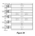
- two 4-aligned LUTsare tied together to form a single tile, in order to save configuration storage and configuration network overhead.
- FIG. 29illustrates the organization of one such tile in some embodiments.
- two sets of 4-aligned LUTs and their associated IMUXs and RMUXsshare five configuration memories.
- the LUTs in each set of 4-aligned LUTsshare one carry chain.
- the addressingis done per half row. When the context is changed for one of the RMUXs in each half row, the context for all RMUXs in that half row is changed.
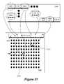
- FIG. 30illustrates a portion of a configurable IC 3000 of some embodiments of the invention.
- this IChas a configurable circuit arrangement 3005 and I/O circuitry 3010 .
- the configurable circuit arrangement 3005can be any of the invention's configurable circuit arrangements that were described above.
- the I/O circuitry 3010is responsible for routing data between the configurable nodes 3015 of the configurable circuit arrangement 3005 and circuits outside of this arrangement (i.e., circuits outside of the IC, or within the IC but outside of the configurable circuit arrangement 3005 ). As further described below, such data includes data that needs to be processed or passed along by the configurable nodes.
- the dataalso includes in some embodiments configuration data that configure the nodes to perform particular operations.
- FIG. 31illustrates a more detailed example of this. Specifically, this figure illustrates a configuration data pool 3105 for the configurable IC 3000 . This pool includes N configuration data sets (CDS). As shown in FIG. 31 , the input/output circuitry 3010 of the configurable IC 3000 routes different configuration data sets to different configurable nodes of the IC 3000 . For instance, FIG. 31 illustrates configurable node 3145 receiving configuration data sets 1 , 3 , and J through the I/O circuitry, while configurable node 3150 receives configuration data sets 3 , K, and N ⁇ 1 through the I/O circuitry.
- CDSconfiguration data sets
- the configuration data setsare stored within each configurable node.
- a configurable nodecan store multiple configuration data sets so that it can reconfigure quickly by changing to another configuration data set.
- some configurable nodesstore only one configuration data set, while other configurable nodes store multiple such data sets.
- FIG. 32illustrates a system on chip (“SoC”) implementation of a configurable IC 3200 .
- This IChas a configurable block 3250 , which includes a configurable circuit arrangement 3105 and I/O circuitry 3110 for this arrangement. It also includes a processor 3215 outside of the configurable circuit arrangement, a memory 3220 , and a bus 3210 , which conceptually represents all conductive paths between the processor 3215 , memory 3220 , and the configurable block 3250 .
- the IC 3200couples to a bus 3230 , which communicatively couples the IC to other circuits, such as an off-chip memory 3225 .
- Bus 3230conceptually represents all conductive paths between the components of the IC 3200 .
- This processor 3215can read and write instructions and/or data from an on-chip memory 3220 or an off-chip memory 3225 .
- the processor 3215can also communicate with the configurable block 3250 through memory 3220 and/or 3225 through buses 3210 and/or 3230 .
- the configurable blockcan retrieve data from and supply data to memories 3220 and 3225 through buses 3210 and 3230 .
- FIG. 33illustrates one such SiP 3300 .
- SiP 3300includes four ICs 3320 , 3325 , 3330 , and 3335 that are stacked on top of each other on a substrate 3305 .
- At least one of these ICsis a configurable IC that includes a configurable block, such as the configurable block 3250 of FIG. 32 .
- Other ICsmight be other circuits, such as processors, memory, etc.
- the ICcommunicatively connects to the substrate 3305 (e.g., through wire bondings 3360 ).
- wire bondingsallow the ICs 3320 - 3335 to communicate with each other without having to go outside of the SiP 3300 .
- the ICs 3320 - 3335might be directly wire-bonded to each other in order to facilitate communication between these ICs. Instead of, or in conjunction with the wire bondings, some embodiments might use other mechanisms to communicatively couple the ICs 3320 - 3335 to each other.
- the SiPincludes a ball grid array (“BGA”) 3310 and a set of vias 3315 .
- the BGA 3310is a set of solder balls that allows the SiP 3300 to be attached to a printed circuit board (“PCB”).
- PCBprinted circuit board
- Each viaconnects a solder ball in the BGA 3310 on the bottom of the substrate 3305 , to a conductor on the top of the substrate 3305 .
- the conductors on the top of the substrate 3305are electrically coupled to the ICs 3320 - 3335 through the wire bondings. Accordingly, the ICs 3320 - 3335 can send and receive signals to and from circuits outside of the SiP 3300 through the wire bondings, the conductors on the top of the substrate 3305 , the set of vias 3315 , and the BGA 3310 .
- the ICs 3320 - 3335can send and receive signals to and from circuits outside of the SiP 3300 through the wire bondings, the conductors on the top of the substrate 3305 , the set of vias 3315 , and the BGA 3310 .
- BGAother embodiments might employ other structures (e.g., a pin grid array) to connect a SiP to circuits outside of the SiP. As shown in FIG.
- a housing 3380encapsulates the substrate 3305 , the BGA 3310 , the set of vias 3315 , the ICs 3320 - 3335 , the wire bondings to form the SiP 3300 .
- This and other SiP structuresare further described in U.S. patent application Ser. No. 11/081,820 entitled “Method for Manufacturing a Programmable System In Package”, filed on Mar. 15, 2005.
- FIG. 34conceptually illustrates a more detailed example of an electronics system 3400 that has an IC 3405 , which implements some of the above described inventions (such as using TMUXs to do multiplication, using TMUXs to utilize Shannon decomposition, etc).
- the system 3400can be a stand-alone computing or communication device, or it can be part of another electronic device. As shown in FIG. 34 , the system 3400 not only includes the IC 3405 , but also includes a bus 3410 , a system memory 3415 , a non-volatile memory 3420 , a storage device 3425 , input devices 3430 , output devices 3435 , and communication interface 3440 .
- the non-volatile memory 3420stores configuration data and re-loads it at power-up. Although the non-volatile memory 3420 is shown outside of the IC 3405 , in some embodiments, the non-volatile memory is either on the same die or the same package as the IC 3405 .
- the bus 3410collectively represents all system, peripheral, and chipset interconnects (including bus and non-bus interconnect structures) that communicatively connect the numerous internal devices of the system 3400 .
- the bus 3410communicatively connects the IC 3410 with the non-volatile memory 3420 , the system memory 3415 , and the permanent storage device 3425 .
- the IC 3405receives data for processing and configuration data for configuring the ICs configurable logic and/or interconnect circuits.
- the IC 3405has a processor, the IC also retrieves from the various memory units instructions to execute.
- the non-volatile memory 3420stores static data and instructions that are needed by the IC 3410 and other modules of the system 3400 .
- the storage device 3425is read-and-write memory device. This device is a non-volatile memory unit that stores instruction and/or data even when the system 3400 is off.
- the system memory 3415is a read-and-write memory device.
- the system memoryis a volatile read-and-write memory, such as a random access memory.
- the system memorystores some of the instructions and/or data that the IC needs at runtime.
- the bus 3410also connects to the input and output devices 3430 and 3435 .
- the input devicesenable the user to enter information into the system 3400 .
- the input devices 3430can include touch-sensitive screens, keys, buttons, keyboards, cursor-controllers, microphone, etc.
- the output devices 3435display the output of the system 3400 .
- bus 3410also couples system 3400 to other devices through a communication interface 3440 .
- Examples of the communication interfaceinclude network adapters that connect to a network of computers, or wired or wireless transceivers for communicating with other devices.
- network adaptersthat connect to a network of computers, or wired or wireless transceivers for communicating with other devices.
- wired or wireless transceiversfor communicating with other devices.
- any other system configurationmay also be used in conjunction with the invention, and these system configurations might have fewer or additional components.
Landscapes
- Engineering & Computer Science (AREA)
- Computer Hardware Design (AREA)
- Physics & Mathematics (AREA)
- General Engineering & Computer Science (AREA)
- Theoretical Computer Science (AREA)
- Evolutionary Computation (AREA)
- Geometry (AREA)
- General Physics & Mathematics (AREA)
- Computing Systems (AREA)
- Mathematical Physics (AREA)
- Logic Circuits (AREA)
- Design And Manufacture Of Integrated Circuits (AREA)
Abstract
Description
2J+2J−1+2J−2+ . . . +2K=2J+1−2K (A)
The Booth algorithm exploits the equality, (A), to create faster multipliers by replacing a sequence of
F(a, b, . . . , n)=[{a·F1(b, . . . , n)}+{ā·F0(b, . . . , n)}] (B)
G(a,b,c,d)=[{a·G1(b,c,d)}+{ā·G0(b,c,d)}]
As shown in
Claims (18)
Priority Applications (1)
| Application Number | Priority Date | Filing Date | Title |
|---|---|---|---|
| US11/754,263US7535252B1 (en) | 2007-03-22 | 2007-05-25 | Configurable ICs that conditionally transition through configuration data sets |
Applications Claiming Priority (2)
| Application Number | Priority Date | Filing Date | Title |
|---|---|---|---|
| US6613507P | 2007-03-22 | 2007-03-22 | |
| US11/754,263US7535252B1 (en) | 2007-03-22 | 2007-05-25 | Configurable ICs that conditionally transition through configuration data sets |
Publications (1)
| Publication Number | Publication Date |
|---|---|
| US7535252B1true US7535252B1 (en) | 2009-05-19 |
Family
ID=40635976
Family Applications (4)
| Application Number | Title | Priority Date | Filing Date |
|---|---|---|---|
| US11/754,263Expired - Fee RelatedUS7535252B1 (en) | 2007-03-22 | 2007-05-25 | Configurable ICs that conditionally transition through configuration data sets |
| US11/754,262Expired - Fee RelatedUS8112468B1 (en) | 2007-03-22 | 2007-05-25 | Method and apparatus for performing an operation with a plurality of sub-operations in a configurable IC |
| US11/754,264Expired - Fee RelatedUS7610566B1 (en) | 2007-03-22 | 2007-05-25 | Method and apparatus for function decomposition |
| US13/344,581AbandonedUS20120098568A1 (en) | 2007-03-22 | 2012-01-05 | Method and apparatus for performing an operation with a plurality of sub-operations in a configurable ic |
Family Applications After (3)
| Application Number | Title | Priority Date | Filing Date |
|---|---|---|---|
| US11/754,262Expired - Fee RelatedUS8112468B1 (en) | 2007-03-22 | 2007-05-25 | Method and apparatus for performing an operation with a plurality of sub-operations in a configurable IC |
| US11/754,264Expired - Fee RelatedUS7610566B1 (en) | 2007-03-22 | 2007-05-25 | Method and apparatus for function decomposition |
| US13/344,581AbandonedUS20120098568A1 (en) | 2007-03-22 | 2012-01-05 | Method and apparatus for performing an operation with a plurality of sub-operations in a configurable ic |
Country Status (1)
| Country | Link |
|---|---|
| US (4) | US7535252B1 (en) |
Cited By (10)
| Publication number | Priority date | Publication date | Assignee | Title |
|---|---|---|---|---|
| US20090219051A1 (en)* | 2006-04-19 | 2009-09-03 | Wei Zhang | Hybrid nanotube/cmos dynamically reconfigurable architecture and an integrated design optimization method and system therefor |
| US20100007376A1 (en)* | 2004-11-08 | 2010-01-14 | Jason Redgrave | Storage elements for a configurable ic and method and apparatus for accessing data stored in the storage elements |
| US20100219859A1 (en)* | 2004-02-14 | 2010-09-02 | Herman Schmit | Non-Sequentially Configurable IC |
| US7804730B2 (en) | 2005-03-15 | 2010-09-28 | Tabula, Inc. | Method and apparatus for accessing contents of memory cells |
| US7825685B2 (en) | 2007-09-06 | 2010-11-02 | Tabula, Inc. | Configuration context switcher with a clocked storage element |
| US7872496B2 (en) | 2004-02-14 | 2011-01-18 | Tabula, Inc. | Method of mapping a user design defined for a user design cycle to an IC with multiple sub-cycle reconfigurable circuits |
| US8112468B1 (en) | 2007-03-22 | 2012-02-07 | Tabula, Inc. | Method and apparatus for performing an operation with a plurality of sub-operations in a configurable IC |
| US20130290693A1 (en)* | 2012-04-27 | 2013-10-31 | Esencia Technologies Inc. | Method and Apparatus for the Automatic Generation of RTL from an Untimed C or C++ Description as a Fine-Grained Specialization of a Micro-processor Soft Core |
| KR20160073334A (en)* | 2014-12-16 | 2016-06-24 | 삼성전자주식회사 | Reconfigurable logic architecture |
| US11323121B2 (en)* | 2017-12-13 | 2022-05-03 | Hercules Microelectronics Co., Ltd. | Programmable device structure based on mixed function storage unit |
Families Citing this family (9)
| Publication number | Priority date | Publication date | Assignee | Title |
|---|---|---|---|---|
| US8392494B2 (en)* | 2009-06-26 | 2013-03-05 | Intel Corporation | Method and apparatus for performing efficient side-channel attack resistant reduction using montgomery or barrett reduction |
| US8201114B1 (en)* | 2009-11-17 | 2012-06-12 | Altera Corporation | Method and apparatus for performing look up table unpacking and repacking for resynthesis |
| EP2553815A1 (en)* | 2010-04-02 | 2013-02-06 | Tabula, Inc. | System and method for reducing reconfiguration power usage |
| US8941409B2 (en) | 2011-07-01 | 2015-01-27 | Tabula, Inc. | Configurable storage elements |
| US9148151B2 (en) | 2011-07-13 | 2015-09-29 | Altera Corporation | Configurable storage elements |
| US9203397B1 (en) | 2011-12-16 | 2015-12-01 | Altera Corporation | Delaying start of user design execution |
| WO2014007845A1 (en)* | 2012-07-02 | 2014-01-09 | Tabula, Inc. | Configurable storage elements |
| US11934799B2 (en)* | 2020-08-19 | 2024-03-19 | SiliconIntervention Inc. | Combinatorial logic circuits with feedback |
| US12099462B1 (en) | 2023-12-08 | 2024-09-24 | Chariot Technologies Lab, Inc. | Dynamic processor architecture |
Citations (172)
| Publication number | Priority date | Publication date | Assignee | Title |
|---|---|---|---|---|
| US4873459A (en) | 1986-09-19 | 1989-10-10 | Actel Corporation | Programmable interconnect architecture |
| US5245575A (en) | 1990-09-07 | 1993-09-14 | Nec Corporation | Register circuit for copying contents of one register into another register |
| US5325329A (en) | 1991-12-03 | 1994-06-28 | Mitsubishi Denki Kabushiki Kaisha | Dual port memory effecting transfer of data between a serial register and an arbitrary memory block |
| US5349250A (en) | 1993-09-02 | 1994-09-20 | Xilinx, Inc. | Logic structure and circuit for fast carry |
| US5357153A (en) | 1993-01-28 | 1994-10-18 | Xilinx, Inc. | Macrocell with product-term cascade and improved flip flop utilization |
| US5365125A (en) | 1992-07-23 | 1994-11-15 | Xilinx, Inc. | Logic cell for field programmable gate array having optional internal feedback and optional cascade |
| US5369622A (en) | 1993-04-20 | 1994-11-29 | Micron Semiconductor, Inc. | Memory with isolated digit lines |
| US5426378A (en)* | 1994-04-20 | 1995-06-20 | Xilinx, Inc. | Programmable logic device which stores more than one configuration and means for switching configurations |
| US5521835A (en) | 1992-03-27 | 1996-05-28 | Xilinx, Inc. | Method for programming an FPLD using a library-based technology mapping algorithm |
| US5532958A (en) | 1990-06-25 | 1996-07-02 | Dallas Semiconductor Corp. | Dual storage cell memory |
| US5552721A (en) | 1995-06-05 | 1996-09-03 | International Business Machines Corporation | Method and system for enhanced drive in programmmable gate arrays |
| US5581500A (en) | 1994-12-16 | 1996-12-03 | Sun Microsystems, Inc. | Memory cell with power supply induced reversed-bias pass transistors for reducing off-leakage current |
| US5600263A (en) | 1995-08-18 | 1997-02-04 | Xilinx, Inc. | Configuration modes for a time multiplexed programmable logic device |
| US5629637A (en) | 1995-08-18 | 1997-05-13 | Xilinx, Inc. | Method of time multiplexing a programmable logic device |
| US5631578A (en) | 1995-06-02 | 1997-05-20 | International Business Machines Corporation | Programmable array interconnect network |
| US5640106A (en) | 1995-05-26 | 1997-06-17 | Xilinx, Inc. | Method and structure for loading data into several IC devices |
| US5646544A (en) | 1995-06-05 | 1997-07-08 | International Business Machines Corporation | System and method for dynamically reconfiguring a programmable gate array |
| US5646545A (en) | 1995-08-18 | 1997-07-08 | Xilinx, Inc. | Time multiplexed programmable logic device |
| US5659484A (en) | 1993-03-29 | 1997-08-19 | Xilinx, Inc. | Frequency driven layout and method for field programmable gate arrays |
| US5682107A (en) | 1994-04-01 | 1997-10-28 | Xilinx, Inc. | FPGA architecture with repeatable tiles including routing matrices and logic matrices |
| US5692147A (en) | 1995-06-07 | 1997-11-25 | International Business Machines Corporation | Memory mapping method and apparatus to fold sparsely populated structures into densely populated memory columns or rows by selectively transposing X and Y address portions, and programmable gate array applications thereof |
| US5701441A (en) | 1995-08-18 | 1997-12-23 | Xilinx, Inc. | Computer-implemented method of optimizing a design in a time multiplexed programmable logic device |
| US5719889A (en) | 1995-12-20 | 1998-02-17 | International Business Machines Corporation | Programmable parity checking and comparison circuit |
| US5732246A (en) | 1995-06-07 | 1998-03-24 | International Business Machines Corporation | Programmable array interconnect latch |
| US5734622A (en) | 1992-09-11 | 1998-03-31 | Fujitsu Limited | MOS static RAM with improved soft error resistance; high-level supply voltage drop detection circuit and complementary signal transition detection circuit for the same; and semiconductor device with improved intersignal time margin |
| US5737235A (en) | 1995-05-02 | 1998-04-07 | Xilinx Inc | FPGA with parallel and serial user interfaces |
| US5745422A (en) | 1996-11-12 | 1998-04-28 | International Business Machines Corporation | Cross-coupled bitline segments for generalized data propagation |
| US5745734A (en) | 1995-09-29 | 1998-04-28 | International Business Machines Corporation | Method and system for programming a gate array using a compressed configuration bit stream |
| US5761483A (en) | 1995-08-18 | 1998-06-02 | Xilinx, Inc. | Optimizing and operating a time multiplexed programmable logic device |
| US5760602A (en) | 1996-01-17 | 1998-06-02 | Hewlett-Packard Company | Time multiplexing a plurality of configuration settings of a programmable switch element in a FPGA |
| US5764954A (en) | 1995-08-23 | 1998-06-09 | International Business Machines Corporation | Method and system for optimizing a critical path in a field programmable gate array configuration |
| US5768178A (en) | 1995-06-30 | 1998-06-16 | Micron Technology, Inc. | Data transfer circuit in a memory device |
| US5777360A (en) | 1994-11-02 | 1998-07-07 | Lsi Logic Corporation | Hexagonal field programmable gate array architecture |
| US5802003A (en) | 1995-12-20 | 1998-09-01 | International Business Machines Corporation | System for implementing write, initialization, and reset in a memory array using a single cell write port |
| US5815726A (en) | 1994-11-04 | 1998-09-29 | Altera Corporation | Coarse-grained look-up table architecture |
| US5889411A (en) | 1997-02-26 | 1999-03-30 | Xilinx, Inc. | FPGA having logic element carry chains capable of generating wide XOR functions |
| US5914616A (en) | 1997-02-26 | 1999-06-22 | Xilinx, Inc. | FPGA repeatable interconnect structure with hierarchical interconnect lines |
| US5914906A (en) | 1995-12-20 | 1999-06-22 | International Business Machines Corporation | Field programmable memory array |
| US5944813A (en) | 1993-08-03 | 1999-08-31 | Xilinx, Inc. | FPGA input output buffer with registered tristate enable |
| US5982655A (en) | 1998-09-29 | 1999-11-09 | Cisco Technology, Inc. | Method and apparatus for support of multiple memory types in a single memory socket architecture |
| US5991191A (en) | 1997-12-05 | 1999-11-23 | Silicon Aquarius, Inc. | Methods and circuits for single-memory cell multivalue data storage |
| US6002991A (en) | 1996-08-30 | 1999-12-14 | Xilinx, Inc. | Method and apparatus for measuring localized voltages on programmable integrated circuits |
| US6054873A (en) | 1996-12-05 | 2000-04-25 | International Business Machines Corporation | Interconnect structure between heterogeneous core regions in a programmable array |
| US6069490A (en) | 1997-12-02 | 2000-05-30 | Xilinx, Inc. | Routing architecture using a direct connect routing mesh |
| US6084429A (en) | 1998-04-24 | 2000-07-04 | Xilinx, Inc. | PLD having a window pane architecture with segmented and staggered interconnect wiring between logic block arrays |
| US6086631A (en) | 1998-04-08 | 2000-07-11 | Xilinx, Inc. | Post-placement residual overlap removal method for core-based PLD programming process |
| US6091263A (en) | 1997-12-12 | 2000-07-18 | Xilinx, Inc. | Rapidly reconfigurable FPGA having a multiple region architecture with reconfiguration caches useable as data RAM |
| US6107821A (en) | 1999-02-08 | 2000-08-22 | Xilinx, Inc. | On-chip logic analysis and method for using the same |
| US6110223A (en) | 1996-10-28 | 2000-08-29 | Altera Corporation | Graphic editor for block diagram level design of circuits |
| US6111779A (en) | 1998-05-07 | 2000-08-29 | Lg Semicon Co., Ltd. | Cell structure for low electric power static RAM |
| US6134154A (en) | 1998-04-03 | 2000-10-17 | Nec Corporation | Semiconductor memory device with several access enabled using single port memory cell |
| US6140839A (en) | 1998-05-13 | 2000-10-31 | Kaviani; Alireza S. | Computational field programmable architecture |
| US6150838A (en) | 1999-02-25 | 2000-11-21 | Xilinx, Inc. | FPGA configurable logic block with multi-purpose logic/memory circuit |
| US6163168A (en) | 1998-12-09 | 2000-12-19 | Vantis Corporation | Efficient interconnect network for use in FPGA device having variable grain architecture |
| US6172521B1 (en) | 1997-04-11 | 2001-01-09 | Nec Corporation | Programmable logic IC having memories for previously storing a plurality of configuration data and a method of reconfigurating same |
| US6173379B1 (en) | 1996-05-14 | 2001-01-09 | Intel Corporation | Memory device for a microprocessor register file having a power management scheme and method for copying information between memory sub-cells in a single clock cycle |
| US6175247B1 (en) | 1998-04-14 | 2001-01-16 | Lockheed Martin Corporation | Context switchable field programmable gate array with public-private addressable sharing of intermediate data |
| US6184707B1 (en) | 1998-10-07 | 2001-02-06 | Altera Corporation | Look-up table based logic element with complete permutability of the inputs to the secondary signals |
| US6184709B1 (en) | 1996-04-09 | 2001-02-06 | Xilinx, Inc. | Programmable logic device having a composable memory array overlaying a CLB array |
| US6205076B1 (en) | 1998-03-27 | 2001-03-20 | Fujitsu Limited | Destructive read type memory circuit, restoring circuit for the same and sense amplifier |
| US6229337B1 (en) | 1999-06-15 | 2001-05-08 | Ict Acquisition, Inc. | High-density programmable logic device with flexible local connections and multiplexer based global interconnections |
| US6255849B1 (en) | 2000-02-04 | 2001-07-03 | Xilinx, Inc. | On-chip self-modification for PLDs |
| US20010007428A1 (en) | 1997-02-26 | 2001-07-12 | Young Steven P. | Interconnect structure for a programmable logic device |
| US6275064B1 (en) | 1997-12-22 | 2001-08-14 | Vantis Corporation | Symmetrical, extended and fast direct connections between variable grain blocks in FPGA integrated circuits |
| US6292019B1 (en)* | 1999-05-07 | 2001-09-18 | Xilinx Inc. | Programmable logic device having configurable logic blocks with user-accessible input multiplexers |
| US20010038552A1 (en) | 2000-03-24 | 2001-11-08 | Kabushiki Kaisha Toshiba | Semiconductor memory with switches for reducing leakage current |
| US6326651B1 (en) | 1999-03-08 | 2001-12-04 | Matsushita Electric Industrial Co., Ltd. | Field-programmable gate array with ferroelectric thin film |
| US6326807B1 (en) | 1997-03-21 | 2001-12-04 | Altera Corporation | Programmable logic architecture incorporating a content addressable embedded array block |
| US20020010853A1 (en) | 1995-08-18 | 2002-01-24 | Xilinx, Inc. | Method of time multiplexing a programmable logic device |
| US6346824B1 (en) | 1996-04-09 | 2002-02-12 | Xilinx, Inc. | Dedicated function fabric for use in field programmable gate arrays |
| US6348813B1 (en) | 1999-06-06 | 2002-02-19 | Lattice Semiconductor Corporation | Scalable architecture for high density CPLD's having two-level hierarchy of routing resources |
| US6381732B1 (en) | 1999-01-14 | 2002-04-30 | Xilinx, Inc. | FPGA customizable to accept selected macros |
| US6404224B1 (en) | 1995-12-19 | 2002-06-11 | Fujitsu Limited | Chain-connected shift register and programmable logic circuit whose logic function is changeable in real time |
| US6411128B2 (en) | 1999-12-10 | 2002-06-25 | Nec Corporation | Logical circuit for serializing and outputting a plurality of signal bits simultaneously read from a memory cell array or the like |
| US6430736B1 (en) | 1999-02-26 | 2002-08-06 | Xilinx, Inc. | Method and apparatus for evolving configuration bitstreams |
| US20020113619A1 (en) | 2000-08-04 | 2002-08-22 | Leopard Logic, Inc. | Interconnection network for a Field Progammable Gate Array |
| US20020125910A1 (en)* | 1999-02-25 | 2002-09-12 | Xilinx, Inc. | Configurable logic element with expander structures |
| US20020125914A1 (en) | 2001-03-08 | 2002-09-12 | Lg Electronics Inc. | Glitch free clock multiplexer circuit and method thereof |
| US6469553B1 (en) | 1999-01-08 | 2002-10-22 | Altera Corporation | Phase-locked loop circuitry for programmable logic devices |
| US6469540B2 (en) | 2000-06-15 | 2002-10-22 | Nec Corporation | Reconfigurable device having programmable interconnect network suitable for implementing data paths |
| US20020161568A1 (en) | 1997-05-30 | 2002-10-31 | Quickturn Design Systems, Inc. | Memory circuit for use in hardware emulation system |
| US20020163357A1 (en) | 1993-08-03 | 2002-11-07 | Btr, Inc. | Architecture and interconnect scheme for programmable logic circuits |
| US6487709B1 (en) | 2000-02-09 | 2002-11-26 | Xilinx, Inc. | Run-time routing for programmable logic devices |
| US6490707B1 (en) | 2000-07-13 | 2002-12-03 | Xilinx, Inc. | Method for converting programmable logic devices into standard cell devices |
| US6496918B1 (en) | 1996-04-11 | 2002-12-17 | Massachusetts Institute Of Technology | Intermediate-grain reconfigurable processing device |
| US6515509B1 (en) | 2000-07-13 | 2003-02-04 | Xilinx, Inc. | Programmable logic device structures in standard cell devices |
| US6515505B1 (en) | 1995-12-26 | 2003-02-04 | Cypress Semiconductor Corp. | Functionality change by bond optioning decoding |
| US6526559B2 (en) | 2001-04-13 | 2003-02-25 | Interface & Control Systems, Inc. | Method for creating circuit redundancy in programmable logic devices |
| US6529040B1 (en) | 2000-05-05 | 2003-03-04 | Xilinx, Inc. | FPGA lookup table with speed read decoder |
| US20030042931A1 (en) | 1993-08-03 | 2003-03-06 | Ting Benjamin S. | Architecture and interconnect scheme for programmable logic circuits |
| US6545501B1 (en) | 2001-12-10 | 2003-04-08 | International Business Machines Corporation | Method and system for use of a field programmable function within a standard cell chip for repair of logic circuits |
| US6560139B2 (en) | 2001-03-05 | 2003-05-06 | Intel Corporation | Low leakage current SRAM array |
| US20030110430A1 (en) | 2001-12-10 | 2003-06-12 | International Business Machines Corporation | Method and system for use of a field programmable gate array (FPGA) function within an application specific integrated circuit (ASIC) to enable creation of a debugger client within the ASIC |
| US20030122578A1 (en)* | 2001-12-28 | 2003-07-03 | Shoichi Masui | Programmable logic device with ferroelectric configuration memories |
| US6593771B2 (en) | 2001-12-10 | 2003-07-15 | International Business Machines Corporation | Method and system for use of a field programmable interconnect within an ASIC for configuring the ASIC |
| US6601227B1 (en) | 2001-06-27 | 2003-07-29 | Xilinx, Inc. | Method for making large-scale ASIC using pre-engineered long distance routing structure |
| US6603330B1 (en) | 2000-10-26 | 2003-08-05 | Cypress Semiconductor Corporation | Configuring digital functions in a digital configurable macro architecture |
| US6629308B1 (en) | 2000-07-13 | 2003-09-30 | Xilinx, Inc. | Method for managing database models for reduced programmable logic device components |
| US6636070B1 (en) | 1997-10-16 | 2003-10-21 | Altera Corp | Driver circuitry for programmable logic devices with hierarchical interconnection resources |
| US6642744B2 (en) | 2000-03-10 | 2003-11-04 | Easic Corporation | Customizable and programmable cell array |
| US6643173B2 (en) | 2001-11-09 | 2003-11-04 | Oki Electric Industry Co., Ltd. | Semiconductor memory device operating in low power supply voltage and low power consumption |
| US6650142B1 (en) | 2002-08-13 | 2003-11-18 | Lattice Semiconductor Corporation | Enhanced CPLD macrocell module having selectable bypass of steering-based resource allocation and methods of use |
| US6668361B2 (en) | 2001-12-10 | 2003-12-23 | International Business Machines Corporation | Method and system for use of a field programmable function within a chip to enable configurable I/O signal timing characteristics |
| US6667635B1 (en) | 2002-09-10 | 2003-12-23 | Xilinx, Inc. | FPGA lookup table with transmission gate structure for reliable low-voltage operation |
| US6675309B1 (en) | 2000-07-13 | 2004-01-06 | Xilinx, Inc. | Method for controlling timing in reduced programmable logic devices |
| US20040010767A1 (en) | 2002-07-12 | 2004-01-15 | Lattice Semiconductor Corporation | Hierarchical general interconnect architecture for high density fpga's |
| US6686769B1 (en) | 2001-12-14 | 2004-02-03 | Altera Corporation | Programmable I/O element circuit for high speed logic devices |
| US6714041B1 (en) | 2002-08-30 | 2004-03-30 | Xilinx, Inc. | Programming on-the-fly (OTF) |
| US6717436B2 (en) | 1999-09-29 | 2004-04-06 | Infineon Technologies Ag | Reconfigurable gate array |
| US6724648B2 (en) | 2002-04-05 | 2004-04-20 | Intel Corporation | SRAM array with dynamic voltage for reducing active leakage power |
| US20040103265A1 (en) | 2002-10-16 | 2004-05-27 | Akya Limited | Reconfigurable integrated circuit |
| US20040105207A1 (en) | 2002-08-09 | 2004-06-03 | Leopard Logic, Inc. | Via programmable gate array interconnect architecture |
| US6798688B2 (en) | 2002-11-29 | 2004-09-28 | International Business Machines Corp. | Storage array such as a SRAM with reduced power requirements |
| US6806730B2 (en) | 2001-12-10 | 2004-10-19 | International Business Machines Corporation | Method and system for use of an embedded field programmable gate array interconnect for flexible I/O connectivity |
| US6809979B1 (en) | 2003-03-04 | 2004-10-26 | Fernandez & Associates, Llp | Complete refresh scheme for 3T dynamic random access memory cells |
| US20040222817A1 (en) | 2002-07-08 | 2004-11-11 | Madurawe Raminda Udaya | Alterable application specific integrated circuit (ASIC) |
| US20040233758A1 (en) | 2003-05-23 | 2004-11-25 | Kim Gi Hong | SRAM-compatible memory device having three sense amplifiers between two memory blocks |
| US6829756B1 (en) | 2002-09-23 | 2004-12-07 | Xilinx, Inc. | Programmable logic device with time-multiplexed interconnect |
| US6831479B2 (en) | 2000-05-03 | 2004-12-14 | Marvell International Ltd. | Circuit for reducing pin count of a semiconductor chip and method for configuring the chip |
| US6838902B1 (en) | 2003-05-28 | 2005-01-04 | Actel Corporation | Synchronous first-in/first-out block memory for a field programmable gate array |
| US6894527B1 (en) | 2003-05-12 | 2005-05-17 | Xilinx, Inc. | Evolved circuits for bitstream protection |
| US6903962B2 (en) | 2003-06-05 | 2005-06-07 | Renesas Technology Corp. | Semiconductor memory device capable of controlling potential level of power supply line and/or ground line |
| US20050128789A1 (en) | 2003-12-11 | 2005-06-16 | Texas Instruments Incorporated | SRAM device and a method of operating the same to reduce leakage current during a sleep mode |
| US20050134308A1 (en) | 2003-12-22 | 2005-06-23 | Sanyo Electric Co., Ltd. | Reconfigurable circuit, processor having reconfigurable circuit, method of determining functions of logic circuits in reconfigurable circuit, method of generating circuit, and circuit |
| US6920627B2 (en) | 2002-12-13 | 2005-07-19 | Xilinx, Inc. | Reconfiguration of a programmable logic device using internal control |
| US6925025B2 (en) | 2003-11-05 | 2005-08-02 | Texas Instruments Incorporated | SRAM device and a method of powering-down the same |
| US6937535B2 (en) | 2002-10-29 | 2005-08-30 | Hynix Semiconductor Inc. | Semiconductor memory device with reduced data access time |
| US6956399B1 (en) | 2004-02-05 | 2005-10-18 | Xilinx, Inc. | High-speed lookup table circuits and methods for programmable logic devices |
| US20050254315A1 (en) | 2002-09-02 | 2005-11-17 | Salters Roelof H W | Device writing to a plurality of rows in a memory matrix simultaneously |
| US6970374B2 (en) | 2004-02-24 | 2005-11-29 | United Microelectronics Corp. | Low leakage current static random access memory |
| US6992505B1 (en) | 2004-03-09 | 2006-01-31 | Xilinx, Inc. | Structures and methods of implementing a pass gate multiplexer with pseudo-differential input signals |
| US6998872B1 (en) | 2004-06-02 | 2006-02-14 | Xilinx, Inc. | Lookup table circuit optionally configurable as two or more smaller lookup tables with independent inputs |
| US7010667B2 (en) | 1997-02-11 | 2006-03-07 | Pact Xpp Technologies Ag | Internal bus system for DFPS and units with two- or multi-dimensional programmable cell architectures, for managing large volumes of data with a high interconnection complexity |
| US7027346B2 (en) | 2003-01-06 | 2006-04-11 | Texas Instruments Incorporated | Bit line control for low power in standby |
| US7030651B2 (en) | 2003-12-04 | 2006-04-18 | Viciciv Technology | Programmable structured arrays |
| US7061941B1 (en) | 2000-11-28 | 2006-06-13 | Winbond Electronics Corporation America | Data input and output circuits for multi-data rate operation |
| US7064577B1 (en) | 2003-05-02 | 2006-06-20 | Altera Corporation | Method and apparatus for supporting variable speed configuration hardware |
| US7075333B1 (en) | 2004-08-24 | 2006-07-11 | Xilinx, Inc. | Programmable circuit optionally configurable as a lookup table or a wide multiplexer |
| US7088136B1 (en) | 2003-11-06 | 2006-08-08 | Altera Corporation | Programmable logic device latch circuits |
| US7107568B2 (en) | 2002-10-07 | 2006-09-12 | Hewlett-Packard Development Company, Lp. | System and method for reducing wire delay or congestion during synthesis of hardware solvers |
| US7110317B2 (en) | 2004-07-02 | 2006-09-19 | Samsung Electronics, Co., Ltd. | SRAM employing virtual rail scheme stable against various process-voltage-temperature variations |
| US7109752B1 (en) | 2004-02-14 | 2006-09-19 | Herman Schmit | Configurable circuits, IC's, and systems |
| US7112992B1 (en) | 2002-10-21 | 2006-09-26 | Altera Corporation | Configuration shift register |
| US7113421B2 (en) | 2004-09-15 | 2006-09-26 | Renesas Technology Corp. | Semiconductor integrated circuit device |
| US7126856B2 (en) | 2000-09-02 | 2006-10-24 | Actel Corporation | Method and apparatus of memory clearing with monitoring RAM memory cells in a field programmable gated array |
| US7126372B2 (en) | 2004-04-30 | 2006-10-24 | Xilinx, Inc. | Reconfiguration port for dynamic reconfiguration—sub-frame access for reconfiguration |
| US7129746B1 (en) | 2003-07-31 | 2006-10-31 | Actel Corporation | System-on-a-chip integrated circuit including dual-function analog and digital inputs |
| US20060250168A1 (en) | 2004-03-09 | 2006-11-09 | Starr Gregory W | Highly configurable PLL architecture for programmable logic |
| US7135886B2 (en) | 2004-09-20 | 2006-11-14 | Klp International, Ltd. | Field programmable gate arrays using both volatile and nonvolatile memory cell properties and their control |
| US7143329B1 (en) | 2001-02-28 | 2006-11-28 | Xilinx, Inc. | FPGA configuration memory with built-in error correction mechanism |
| US7145829B1 (en) | 2005-06-16 | 2006-12-05 | International Business Machines Corporation | Single cycle refresh of multi-port dynamic random access memory (DRAM) |
| US7154299B2 (en) | 2002-04-05 | 2006-12-26 | Stmicroelectronics Pvt. Ltd. | Architecture for programmable logic device |
| US7167025B1 (en) | 2004-02-14 | 2007-01-23 | Herman Schmit | Non-sequentially configurable IC |
| US7193440B1 (en) | 2004-02-14 | 2007-03-20 | Herman Schmit | Configurable circuits, IC's, and systems |
| US7200235B1 (en) | 2002-03-29 | 2007-04-03 | Xilinx, Inc. | Error-checking and correcting decryption-key memory for programmable logic devices |
| US7209404B2 (en) | 2005-08-05 | 2007-04-24 | Fortemedia Inc. | Low power memory sub-system architecture |
| US7212448B1 (en) | 2005-07-19 | 2007-05-01 | Xilinx, Inc. | Method and apparatus for multiple context and high reliability operation of programmable logic devices |
| US7224182B1 (en) | 2005-03-15 | 2007-05-29 | Brad Hutchings | Hybrid configurable circuit for a configurable IC |
| US7224181B1 (en) | 2004-11-08 | 2007-05-29 | Herman Schmit | Clock distribution in a configurable IC |
| US7230869B1 (en) | 2005-03-15 | 2007-06-12 | Jason Redgrave | Method and apparatus for accessing contents of memory cells |
| US20070143577A1 (en) | 2002-10-16 | 2007-06-21 | Akya (Holdings) Limited | Reconfigurable integrated circuit |
| US7236009B1 (en) | 2004-12-01 | 2007-06-26 | Andre Rohe | Operational time extension |
| US7268586B1 (en) | 2004-11-08 | 2007-09-11 | Tabula, Inc. | Method and apparatus for accessing stored data in a reconfigurable IC |
| US7272031B1 (en) | 2005-03-15 | 2007-09-18 | Tabula, Inc. | Method and apparatus for reduced power cell |
| US7276933B1 (en) | 2004-11-08 | 2007-10-02 | Tabula, Inc. | Reconfigurable IC that has sections running at different looperness |
| US20070257700A1 (en) | 2005-03-15 | 2007-11-08 | Andrew Caldwell | Method and apparatus for decomposing functions in a configurable IC |
| US7295037B2 (en) | 2004-11-08 | 2007-11-13 | Tabula, Inc. | Configurable IC with routing circuits with offset connections |
| US7304904B2 (en) | 2005-03-04 | 2007-12-04 | Atmel Corporation | Fast read port for register file |
| US7317331B2 (en) | 2004-11-08 | 2008-01-08 | Tabula, Inc. | Reconfigurable IC that has sections running at different reconfiguration rates |
| US7330050B2 (en) | 2004-11-08 | 2008-02-12 | Tabula, Inc. | Storage elements for a configurable IC and method and apparatus for accessing data stored in the storage elements |
| US7342415B2 (en) | 2004-11-08 | 2008-03-11 | Tabula, Inc. | Configurable IC with interconnect circuits that also perform storage operations |
| US7425841B2 (en) | 2004-02-14 | 2008-09-16 | Tabula Inc. | Configurable circuits, IC's, and systems |
Family Cites Families (49)
| Publication number | Priority date | Publication date | Assignee | Title |
|---|---|---|---|---|
| JPS57141753A (en)* | 1981-02-25 | 1982-09-02 | Nec Corp | Multiplication circuit |
| US5544078A (en) | 1988-06-17 | 1996-08-06 | Dallas Semiconductor Corporation | Timekeeping comparison circuitry and dual storage memory cells to detect alarms |
| JP2743526B2 (en) | 1989-10-23 | 1998-04-22 | 日本電気株式会社 | Register circuit |
| JP2944243B2 (en) | 1991-04-15 | 1999-08-30 | 日本電気株式会社 | Semiconductor integrated circuit |
| JPH05274860A (en) | 1992-03-26 | 1993-10-22 | Nec Corp | Semiconductor memory |
| US5329498A (en) | 1993-05-17 | 1994-07-12 | Hewlett-Packard Company | Signal conditioning and interconnection for an acoustic transducer |
| SG46393A1 (en) | 1993-05-28 | 1998-02-20 | Univ California | Field programmable logic device with dynamic interconnections to a dynamic logic core |
| IL109921A (en) | 1993-06-24 | 1997-09-30 | Quickturn Design Systems | Method and apparatus for configuring memory circuits |
| US5847577A (en) | 1995-02-24 | 1998-12-08 | Xilinx, Inc. | DRAM memory cell for programmable logic devices |
| US5721498A (en) | 1995-12-11 | 1998-02-24 | Hewlett Packard Company | Block segmentation of configuration lines for fault tolerant programmable logic device |
| US5958000A (en)* | 1996-11-15 | 1999-09-28 | Samsung Electronics, Co. Ltd. | Two-bit booth multiplier with reduced data path width |
| US6057707A (en) | 1997-06-20 | 2000-05-02 | Altera Corporation | Programmable logic device incorporating a memory efficient interconnection device |
| US5970240A (en) | 1997-06-25 | 1999-10-19 | Quickturn Design Systems, Inc. | Method and apparatus for configurable memory emulation |
| US6204687B1 (en) | 1999-08-13 | 2001-03-20 | Xilinx, Inc. | Method and structure for configuring FPGAS |
| US6166946A (en) | 2000-01-21 | 2000-12-26 | Hewlett-Packard Company | System and method for writing to and reading from a memory cell |
| JP2001217707A (en)* | 2000-01-31 | 2001-08-10 | Sony Corp | Logic cell and logic circuit using the same |
| JP2002074941A (en) | 2000-08-23 | 2002-03-15 | Nec Corp | Multiple line buffer type memory LSI |
| JP2002083001A (en)* | 2000-09-06 | 2002-03-22 | Hitachi Ltd | Logic circuit design method and cell library used therefor |
| US6501698B1 (en) | 2000-11-01 | 2002-12-31 | Enhanced Memory Systems, Inc. | Structure and method for hiding DRAM cycle time behind a burst access |
| JP2002197867A (en) | 2000-12-28 | 2002-07-12 | Nec Corp | Semiconductor device |
| JP2003058426A (en) | 2001-08-21 | 2003-02-28 | Sony Corp | Integrated circuit, and its circuit constituting method and program |
| JP4856848B2 (en) | 2001-10-11 | 2012-01-18 | アルテラ コーポレイション | Error detection on programmable logic resources |
| JP2003132683A (en) | 2001-10-23 | 2003-05-09 | Hitachi Ltd | Semiconductor device |
| US6552949B1 (en) | 2002-02-05 | 2003-04-22 | Arm Limited | Reducing leakage current in a memory device |
| US6791352B2 (en) | 2002-02-08 | 2004-09-14 | International Business Machines Corporation | Method and apparatus for debugging a chip |
| US6911842B1 (en) | 2002-03-01 | 2005-06-28 | Xilinx, Inc. | Low jitter clock for a physical media access sublayer on a field programmable gate array |
| US6747478B2 (en) | 2002-07-08 | 2004-06-08 | Viciciv | Field programmable gate array with convertibility to application specific integrated circuit |
| US6992503B2 (en) | 2002-07-08 | 2006-01-31 | Viciciv Technology | Programmable devices with convertibility to customizable devices |
| EP1676208A2 (en) | 2003-08-28 | 2006-07-05 | PACT XPP Technologies AG | Data processing device and method |
| US7308470B2 (en)* | 2003-12-05 | 2007-12-11 | Intel Corporation | Smaller and lower power static mux circuitry in generating multiplier partial product signals |
| US7218137B2 (en) | 2004-04-30 | 2007-05-15 | Xilinx, Inc. | Reconfiguration port for dynamic reconfiguration |
| US6937172B1 (en) | 2004-05-04 | 2005-08-30 | Xilinx, Inc. | Method and system for gray-coding counting |
| US7376774B1 (en) | 2004-08-27 | 2008-05-20 | Xilinx, Inc. | Network media access controller embedded in a programmable logic device—host interface control generator |
| US7116131B1 (en) | 2004-09-15 | 2006-10-03 | Xilinx, Inc. | High performance programmable logic devices utilizing dynamic circuitry |
| US7417918B1 (en) | 2004-09-29 | 2008-08-26 | Xilinx, Inc. | Method and apparatus for configuring the operating speed of a programmable logic device through a self-timed reference circuit |
| US7424655B1 (en) | 2004-10-01 | 2008-09-09 | Xilinx, Inc. | Utilizing multiple test bitstreams to avoid localized defects in partially defective programmable integrated circuits |
| US7136308B2 (en) | 2004-11-01 | 2006-11-14 | Sun Microsystems, Inc. | Efficient method of data transfer between register files and memories |
| US7203100B2 (en) | 2004-11-01 | 2007-04-10 | Sun Mircosystems, Inc. | Efficient implementation of a read scheme for multi-threaded register file |
| DE102005023118B3 (en) | 2005-05-19 | 2006-12-21 | Infineon Technologies Ag | Circuit arrangement for supplying configuration data in FPGA devices |
| JP4900717B2 (en)* | 2005-05-31 | 2012-03-21 | 富士ゼロックス株式会社 | Reconfigurable device |
| US7443196B2 (en) | 2005-07-15 | 2008-10-28 | Tabula, Inc. | Configuration network for a configurable IC |
| US7375550B1 (en) | 2005-07-15 | 2008-05-20 | Tabula, Inc. | Configurable IC with packet switch configuration network |
| JP2007058419A (en) | 2005-08-23 | 2007-03-08 | Hitachi Ltd | Storage system having logic circuit constructed according to information in memory on PLD |
| US7328384B1 (en) | 2005-09-29 | 2008-02-05 | Xilinx, Inc. | Method and apparatus using device defects as an identifier |
| US7529992B1 (en) | 2006-03-27 | 2009-05-05 | Tabula, Inc. | Configurable integrated circuit with error correcting circuitry |
| US7669097B1 (en) | 2006-03-27 | 2010-02-23 | Tabula, Inc. | Configurable IC with error detection and correction circuitry |
| US7535252B1 (en) | 2007-03-22 | 2009-05-19 | Tabula, Inc. | Configurable ICs that conditionally transition through configuration data sets |
| US8344755B2 (en) | 2007-09-06 | 2013-01-01 | Tabula, Inc. | Configuration context switcher |
| US7986878B2 (en) | 2008-02-05 | 2011-07-26 | Opnext Subsystems, Inc. | Adjustable bit rate optical transmission using programmable signal modulation |
- 2007
- 2007-05-25USUS11/754,263patent/US7535252B1/ennot_activeExpired - Fee Related
- 2007-05-25USUS11/754,262patent/US8112468B1/ennot_activeExpired - Fee Related
- 2007-05-25USUS11/754,264patent/US7610566B1/ennot_activeExpired - Fee Related
- 2012
- 2012-01-05USUS13/344,581patent/US20120098568A1/ennot_activeAbandoned
Patent Citations (206)
| Publication number | Priority date | Publication date | Assignee | Title |
|---|---|---|---|---|
| US4873459A (en) | 1986-09-19 | 1989-10-10 | Actel Corporation | Programmable interconnect architecture |
| US4873459B1 (en) | 1986-09-19 | 1995-01-10 | Actel Corp | Programmable interconnect architecture |
| US5532958A (en) | 1990-06-25 | 1996-07-02 | Dallas Semiconductor Corp. | Dual storage cell memory |
| US5245575A (en) | 1990-09-07 | 1993-09-14 | Nec Corporation | Register circuit for copying contents of one register into another register |
| US5325329A (en) | 1991-12-03 | 1994-06-28 | Mitsubishi Denki Kabushiki Kaisha | Dual port memory effecting transfer of data between a serial register and an arbitrary memory block |
| US5610829A (en) | 1992-03-27 | 1997-03-11 | Xilinx, Inc. | Method for programming an FPLD using a library-based technology mapping algorithm |
| US5521835A (en) | 1992-03-27 | 1996-05-28 | Xilinx, Inc. | Method for programming an FPLD using a library-based technology mapping algorithm |
| US5365125A (en) | 1992-07-23 | 1994-11-15 | Xilinx, Inc. | Logic cell for field programmable gate array having optional internal feedback and optional cascade |
| US5734622A (en) | 1992-09-11 | 1998-03-31 | Fujitsu Limited | MOS static RAM with improved soft error resistance; high-level supply voltage drop detection circuit and complementary signal transition detection circuit for the same; and semiconductor device with improved intersignal time margin |
| US5357153A (en) | 1993-01-28 | 1994-10-18 | Xilinx, Inc. | Macrocell with product-term cascade and improved flip flop utilization |
| US5659484A (en) | 1993-03-29 | 1997-08-19 | Xilinx, Inc. | Frequency driven layout and method for field programmable gate arrays |
| US5369622A (en) | 1993-04-20 | 1994-11-29 | Micron Semiconductor, Inc. | Memory with isolated digit lines |
| US20030042931A1 (en) | 1993-08-03 | 2003-03-06 | Ting Benjamin S. | Architecture and interconnect scheme for programmable logic circuits |
| US5944813A (en) | 1993-08-03 | 1999-08-31 | Xilinx, Inc. | FPGA input output buffer with registered tristate enable |
| US6703861B2 (en) | 1993-08-03 | 2004-03-09 | Btr, Inc. | Architecture and interconnect scheme for programmable logic circuits |
| US20020163357A1 (en) | 1993-08-03 | 2002-11-07 | Btr, Inc. | Architecture and interconnect scheme for programmable logic circuits |
| US20040196066A1 (en) | 1993-08-03 | 2004-10-07 | Ting Benjamin S. | Architecture and interconnect scheme for programmable logic circuits |
| US5349250A (en) | 1993-09-02 | 1994-09-20 | Xilinx, Inc. | Logic structure and circuit for fast carry |
| US5682107A (en) | 1994-04-01 | 1997-10-28 | Xilinx, Inc. | FPGA architecture with repeatable tiles including routing matrices and logic matrices |
| US5426378A (en)* | 1994-04-20 | 1995-06-20 | Xilinx, Inc. | Programmable logic device which stores more than one configuration and means for switching configurations |
| US5777360A (en) | 1994-11-02 | 1998-07-07 | Lsi Logic Corporation | Hexagonal field programmable gate array architecture |
| US5815726A (en) | 1994-11-04 | 1998-09-29 | Altera Corporation | Coarse-grained look-up table architecture |
| US5581500A (en) | 1994-12-16 | 1996-12-03 | Sun Microsystems, Inc. | Memory cell with power supply induced reversed-bias pass transistors for reducing off-leakage current |
| US5737235A (en) | 1995-05-02 | 1998-04-07 | Xilinx Inc | FPGA with parallel and serial user interfaces |
| US5640106A (en) | 1995-05-26 | 1997-06-17 | Xilinx, Inc. | Method and structure for loading data into several IC devices |
| US5631578A (en) | 1995-06-02 | 1997-05-20 | International Business Machines Corporation | Programmable array interconnect network |
| US5694057A (en) | 1995-06-05 | 1997-12-02 | International Business Machines Corporation | System for enhanced drive in programmable gate arrays |
| US5552721A (en) | 1995-06-05 | 1996-09-03 | International Business Machines Corporation | Method and system for enhanced drive in programmmable gate arrays |
| US5646544A (en) | 1995-06-05 | 1997-07-08 | International Business Machines Corporation | System and method for dynamically reconfiguring a programmable gate array |
| US5732246A (en) | 1995-06-07 | 1998-03-24 | International Business Machines Corporation | Programmable array interconnect latch |
| US5692147A (en) | 1995-06-07 | 1997-11-25 | International Business Machines Corporation | Memory mapping method and apparatus to fold sparsely populated structures into densely populated memory columns or rows by selectively transposing X and Y address portions, and programmable gate array applications thereof |
| US5768178A (en) | 1995-06-30 | 1998-06-16 | Micron Technology, Inc. | Data transfer circuit in a memory device |
| US6480954B2 (en) | 1995-08-18 | 2002-11-12 | Xilinx Inc. | Method of time multiplexing a programmable logic device |
| US5646545A (en) | 1995-08-18 | 1997-07-08 | Xilinx, Inc. | Time multiplexed programmable logic device |
| US20020010853A1 (en) | 1995-08-18 | 2002-01-24 | Xilinx, Inc. | Method of time multiplexing a programmable logic device |
| US5701441A (en) | 1995-08-18 | 1997-12-23 | Xilinx, Inc. | Computer-implemented method of optimizing a design in a time multiplexed programmable logic device |
| US5825662A (en) | 1995-08-18 | 1998-10-20 | Xilinx, Inc. | Computer-implemented method of optimizing a time multiplexed programmable logic device |
| US5629637A (en) | 1995-08-18 | 1997-05-13 | Xilinx, Inc. | Method of time multiplexing a programmable logic device |
| US5600263A (en) | 1995-08-18 | 1997-02-04 | Xilinx, Inc. | Configuration modes for a time multiplexed programmable logic device |
| US5761483A (en) | 1995-08-18 | 1998-06-02 | Xilinx, Inc. | Optimizing and operating a time multiplexed programmable logic device |
| US5764954A (en) | 1995-08-23 | 1998-06-09 | International Business Machines Corporation | Method and system for optimizing a critical path in a field programmable gate array configuration |
| US5745734A (en) | 1995-09-29 | 1998-04-28 | International Business Machines Corporation | Method and system for programming a gate array using a compressed configuration bit stream |
| US6404224B1 (en) | 1995-12-19 | 2002-06-11 | Fujitsu Limited | Chain-connected shift register and programmable logic circuit whose logic function is changeable in real time |
| US6130854A (en) | 1995-12-20 | 2000-10-10 | International Business Machines Corporation | Programmable address decoder for field programmable memory array |
| US6233191B1 (en) | 1995-12-20 | 2001-05-15 | International Business Machines Corporation | Field programmable memory array |
| US5719889A (en) | 1995-12-20 | 1998-02-17 | International Business Machines Corporation | Programmable parity checking and comparison circuit |
| US6023421A (en) | 1995-12-20 | 2000-02-08 | International Business Machines Corporation | Selective connectivity between memory sub-arrays and a hierarchical bit line structure in a memory array |
| US6038192A (en) | 1995-12-20 | 2000-03-14 | International Business Machines Corporation | Memory cells for field programmable memory array |
| US6044031A (en) | 1995-12-20 | 2000-03-28 | International Business Machines Corporation | Programmable bit line drive modes for memory arrays |
| US6118707A (en) | 1995-12-20 | 2000-09-12 | International Business Machines Corporation | Method of operating a field programmable memory array with a field programmable gate array |
| US5802003A (en) | 1995-12-20 | 1998-09-01 | International Business Machines Corporation | System for implementing write, initialization, and reset in a memory array using a single cell write port |
| US6075745A (en) | 1995-12-20 | 2000-06-13 | International Business Machines Corporation | Field programmable memory array |
| US5914906A (en) | 1995-12-20 | 1999-06-22 | International Business Machines Corporation | Field programmable memory array |
| US6091645A (en) | 1995-12-20 | 2000-07-18 | International Business Machines Corporation | Programmable read ports and write ports for I/O buses in a field programmable memory array |
| US6515505B1 (en) | 1995-12-26 | 2003-02-04 | Cypress Semiconductor Corp. | Functionality change by bond optioning decoding |
| US5760602A (en) | 1996-01-17 | 1998-06-02 | Hewlett-Packard Company | Time multiplexing a plurality of configuration settings of a programmable switch element in a FPGA |
| US6184709B1 (en) | 1996-04-09 | 2001-02-06 | Xilinx, Inc. | Programmable logic device having a composable memory array overlaying a CLB array |
| US6346824B1 (en) | 1996-04-09 | 2002-02-12 | Xilinx, Inc. | Dedicated function fabric for use in field programmable gate arrays |
| US6496918B1 (en) | 1996-04-11 | 2002-12-17 | Massachusetts Institute Of Technology | Intermediate-grain reconfigurable processing device |
| US6173379B1 (en) | 1996-05-14 | 2001-01-09 | Intel Corporation | Memory device for a microprocessor register file having a power management scheme and method for copying information between memory sub-cells in a single clock cycle |
| US6002991A (en) | 1996-08-30 | 1999-12-14 | Xilinx, Inc. | Method and apparatus for measuring localized voltages on programmable integrated circuits |
| US6110223A (en) | 1996-10-28 | 2000-08-29 | Altera Corporation | Graphic editor for block diagram level design of circuits |
| US5745422A (en) | 1996-11-12 | 1998-04-28 | International Business Machines Corporation | Cross-coupled bitline segments for generalized data propagation |
| US6054873A (en) | 1996-12-05 | 2000-04-25 | International Business Machines Corporation | Interconnect structure between heterogeneous core regions in a programmable array |
| US7010667B2 (en) | 1997-02-11 | 2006-03-07 | Pact Xpp Technologies Ag | Internal bus system for DFPS and units with two- or multi-dimensional programmable cell architectures, for managing large volumes of data with a high interconnection complexity |
| US20010007428A1 (en) | 1997-02-26 | 2001-07-12 | Young Steven P. | Interconnect structure for a programmable logic device |
| US5914616A (en) | 1997-02-26 | 1999-06-22 | Xilinx, Inc. | FPGA repeatable interconnect structure with hierarchical interconnect lines |
| US5889411A (en) | 1997-02-26 | 1999-03-30 | Xilinx, Inc. | FPGA having logic element carry chains capable of generating wide XOR functions |
| US20020008541A1 (en) | 1997-02-26 | 2002-01-24 | Xilinx, Inc. | Interconnect structure for a programmable logic device |
| US6326807B1 (en) | 1997-03-21 | 2001-12-04 | Altera Corporation | Programmable logic architecture incorporating a content addressable embedded array block |
| US6172521B1 (en) | 1997-04-11 | 2001-01-09 | Nec Corporation | Programmable logic IC having memories for previously storing a plurality of configuration data and a method of reconfigurating same |
| US20020161568A1 (en) | 1997-05-30 | 2002-10-31 | Quickturn Design Systems, Inc. | Memory circuit for use in hardware emulation system |
| US6732068B2 (en) | 1997-05-30 | 2004-05-04 | Quickturn Design Systems Inc. | Memory circuit for use in hardware emulation system |
| US6636070B1 (en) | 1997-10-16 | 2003-10-21 | Altera Corp | Driver circuitry for programmable logic devices with hierarchical interconnection resources |
| US6069490A (en) | 1997-12-02 | 2000-05-30 | Xilinx, Inc. | Routing architecture using a direct connect routing mesh |
| US5991191A (en) | 1997-12-05 | 1999-11-23 | Silicon Aquarius, Inc. | Methods and circuits for single-memory cell multivalue data storage |
| US6091263A (en) | 1997-12-12 | 2000-07-18 | Xilinx, Inc. | Rapidly reconfigurable FPGA having a multiple region architecture with reconfiguration caches useable as data RAM |
| US6275064B1 (en) | 1997-12-22 | 2001-08-14 | Vantis Corporation | Symmetrical, extended and fast direct connections between variable grain blocks in FPGA integrated circuits |
| US6205076B1 (en) | 1998-03-27 | 2001-03-20 | Fujitsu Limited | Destructive read type memory circuit, restoring circuit for the same and sense amplifier |
| US6134154A (en) | 1998-04-03 | 2000-10-17 | Nec Corporation | Semiconductor memory device with several access enabled using single port memory cell |
| US6086631A (en) | 1998-04-08 | 2000-07-11 | Xilinx, Inc. | Post-placement residual overlap removal method for core-based PLD programming process |
| US6175247B1 (en) | 1998-04-14 | 2001-01-16 | Lockheed Martin Corporation | Context switchable field programmable gate array with public-private addressable sharing of intermediate data |
| US6084429A (en) | 1998-04-24 | 2000-07-04 | Xilinx, Inc. | PLD having a window pane architecture with segmented and staggered interconnect wiring between logic block arrays |
| US6111779A (en) | 1998-05-07 | 2000-08-29 | Lg Semicon Co., Ltd. | Cell structure for low electric power static RAM |
| US6140839A (en) | 1998-05-13 | 2000-10-31 | Kaviani; Alireza S. | Computational field programmable architecture |
| US5982655A (en) | 1998-09-29 | 1999-11-09 | Cisco Technology, Inc. | Method and apparatus for support of multiple memory types in a single memory socket architecture |
| US6184707B1 (en) | 1998-10-07 | 2001-02-06 | Altera Corporation | Look-up table based logic element with complete permutability of the inputs to the secondary signals |
| US6163168A (en) | 1998-12-09 | 2000-12-19 | Vantis Corporation | Efficient interconnect network for use in FPGA device having variable grain architecture |
| US6469553B1 (en) | 1999-01-08 | 2002-10-22 | Altera Corporation | Phase-locked loop circuitry for programmable logic devices |
| US6381732B1 (en) | 1999-01-14 | 2002-04-30 | Xilinx, Inc. | FPGA customizable to accept selected macros |
| US6107821A (en) | 1999-02-08 | 2000-08-22 | Xilinx, Inc. | On-chip logic analysis and method for using the same |
| US6150838A (en) | 1999-02-25 | 2000-11-21 | Xilinx, Inc. | FPGA configurable logic block with multi-purpose logic/memory circuit |
| US20020125910A1 (en)* | 1999-02-25 | 2002-09-12 | Xilinx, Inc. | Configurable logic element with expander structures |
| US6430736B1 (en) | 1999-02-26 | 2002-08-06 | Xilinx, Inc. | Method and apparatus for evolving configuration bitstreams |
| US6326651B1 (en) | 1999-03-08 | 2001-12-04 | Matsushita Electric Industrial Co., Ltd. | Field-programmable gate array with ferroelectric thin film |
| US6292019B1 (en)* | 1999-05-07 | 2001-09-18 | Xilinx Inc. | Programmable logic device having configurable logic blocks with user-accessible input multiplexers |
| US6348813B1 (en) | 1999-06-06 | 2002-02-19 | Lattice Semiconductor Corporation | Scalable architecture for high density CPLD's having two-level hierarchy of routing resources |
| US6229337B1 (en) | 1999-06-15 | 2001-05-08 | Ict Acquisition, Inc. | High-density programmable logic device with flexible local connections and multiplexer based global interconnections |
| US6717436B2 (en) | 1999-09-29 | 2004-04-06 | Infineon Technologies Ag | Reconfigurable gate array |
| US6411128B2 (en) | 1999-12-10 | 2002-06-25 | Nec Corporation | Logical circuit for serializing and outputting a plurality of signal bits simultaneously read from a memory cell array or the like |
| US6255849B1 (en) | 2000-02-04 | 2001-07-03 | Xilinx, Inc. | On-chip self-modification for PLDs |
| US6487709B1 (en) | 2000-02-09 | 2002-11-26 | Xilinx, Inc. | Run-time routing for programmable logic devices |
| US6642744B2 (en) | 2000-03-10 | 2003-11-04 | Easic Corporation | Customizable and programmable cell array |
| US20010038552A1 (en) | 2000-03-24 | 2001-11-08 | Kabushiki Kaisha Toshiba | Semiconductor memory with switches for reducing leakage current |
| US6831479B2 (en) | 2000-05-03 | 2004-12-14 | Marvell International Ltd. | Circuit for reducing pin count of a semiconductor chip and method for configuring the chip |
| US6529040B1 (en) | 2000-05-05 | 2003-03-04 | Xilinx, Inc. | FPGA lookup table with speed read decoder |
| US6469540B2 (en) | 2000-06-15 | 2002-10-22 | Nec Corporation | Reconfigurable device having programmable interconnect network suitable for implementing data paths |
| US20030080777A1 (en) | 2000-07-13 | 2003-05-01 | Xilinx, Inc. | Programmable logic device structures in standard cell devices |
| US6515509B1 (en) | 2000-07-13 | 2003-02-04 | Xilinx, Inc. | Programmable logic device structures in standard cell devices |
| US6490707B1 (en) | 2000-07-13 | 2002-12-03 | Xilinx, Inc. | Method for converting programmable logic devices into standard cell devices |
| US6675309B1 (en) | 2000-07-13 | 2004-01-06 | Xilinx, Inc. | Method for controlling timing in reduced programmable logic devices |
| US6629308B1 (en) | 2000-07-13 | 2003-09-30 | Xilinx, Inc. | Method for managing database models for reduced programmable logic device components |
| US20020113619A1 (en) | 2000-08-04 | 2002-08-22 | Leopard Logic, Inc. | Interconnection network for a Field Progammable Gate Array |
| US7126856B2 (en) | 2000-09-02 | 2006-10-24 | Actel Corporation | Method and apparatus of memory clearing with monitoring RAM memory cells in a field programmable gated array |
| US6603330B1 (en) | 2000-10-26 | 2003-08-05 | Cypress Semiconductor Corporation | Configuring digital functions in a digital configurable macro architecture |
| US7061941B1 (en) | 2000-11-28 | 2006-06-13 | Winbond Electronics Corporation America | Data input and output circuits for multi-data rate operation |
| US7143329B1 (en) | 2001-02-28 | 2006-11-28 | Xilinx, Inc. | FPGA configuration memory with built-in error correction mechanism |
| US6560139B2 (en) | 2001-03-05 | 2003-05-06 | Intel Corporation | Low leakage current SRAM array |
| US20020125914A1 (en) | 2001-03-08 | 2002-09-12 | Lg Electronics Inc. | Glitch free clock multiplexer circuit and method thereof |
| US6526559B2 (en) | 2001-04-13 | 2003-02-25 | Interface & Control Systems, Inc. | Method for creating circuit redundancy in programmable logic devices |
| US6601227B1 (en) | 2001-06-27 | 2003-07-29 | Xilinx, Inc. | Method for making large-scale ASIC using pre-engineered long distance routing structure |
| US6643173B2 (en) | 2001-11-09 | 2003-11-04 | Oki Electric Industry Co., Ltd. | Semiconductor memory device operating in low power supply voltage and low power consumption |
| US6668361B2 (en) | 2001-12-10 | 2003-12-23 | International Business Machines Corporation | Method and system for use of a field programmable function within a chip to enable configurable I/O signal timing characteristics |
| US6806730B2 (en) | 2001-12-10 | 2004-10-19 | International Business Machines Corporation | Method and system for use of an embedded field programmable gate array interconnect for flexible I/O connectivity |
| US6593771B2 (en) | 2001-12-10 | 2003-07-15 | International Business Machines Corporation | Method and system for use of a field programmable interconnect within an ASIC for configuring the ASIC |
| US6545501B1 (en) | 2001-12-10 | 2003-04-08 | International Business Machines Corporation | Method and system for use of a field programmable function within a standard cell chip for repair of logic circuits |
| US20030110430A1 (en) | 2001-12-10 | 2003-06-12 | International Business Machines Corporation | Method and system for use of a field programmable gate array (FPGA) function within an application specific integrated circuit (ASIC) to enable creation of a debugger client within the ASIC |
| US6686769B1 (en) | 2001-12-14 | 2004-02-03 | Altera Corporation | Programmable I/O element circuit for high speed logic devices |
| US6924663B2 (en) | 2001-12-28 | 2005-08-02 | Fujitsu Limited | Programmable logic device with ferroelectric configuration memories |
| US20030122578A1 (en)* | 2001-12-28 | 2003-07-03 | Shoichi Masui | Programmable logic device with ferroelectric configuration memories |
| US7200235B1 (en) | 2002-03-29 | 2007-04-03 | Xilinx, Inc. | Error-checking and correcting decryption-key memory for programmable logic devices |
| US7154299B2 (en) | 2002-04-05 | 2006-12-26 | Stmicroelectronics Pvt. Ltd. | Architecture for programmable logic device |
| US6724648B2 (en) | 2002-04-05 | 2004-04-20 | Intel Corporation | SRAM array with dynamic voltage for reducing active leakage power |
| US20040222817A1 (en) | 2002-07-08 | 2004-11-11 | Madurawe Raminda Udaya | Alterable application specific integrated circuit (ASIC) |
| US7028281B1 (en) | 2002-07-12 | 2006-04-11 | Lattice Semiconductor Corporation | FPGA with register-intensive architecture |
| US20040010767A1 (en) | 2002-07-12 | 2004-01-15 | Lattice Semiconductor Corporation | Hierarchical general interconnect architecture for high density fpga's |
| US20040105207A1 (en) | 2002-08-09 | 2004-06-03 | Leopard Logic, Inc. | Via programmable gate array interconnect architecture |
| US6650142B1 (en) | 2002-08-13 | 2003-11-18 | Lattice Semiconductor Corporation | Enhanced CPLD macrocell module having selectable bypass of steering-based resource allocation and methods of use |
| US6714041B1 (en) | 2002-08-30 | 2004-03-30 | Xilinx, Inc. | Programming on-the-fly (OTF) |
| US20050254315A1 (en) | 2002-09-02 | 2005-11-17 | Salters Roelof H W | Device writing to a plurality of rows in a memory matrix simultaneously |
| US6667635B1 (en) | 2002-09-10 | 2003-12-23 | Xilinx, Inc. | FPGA lookup table with transmission gate structure for reliable low-voltage operation |
| US7138827B1 (en) | 2002-09-23 | 2006-11-21 | Xilinx, Inc. | Programmable logic device with time-multiplexed interconnect |
| US6829756B1 (en) | 2002-09-23 | 2004-12-07 | Xilinx, Inc. | Programmable logic device with time-multiplexed interconnect |
| US7107568B2 (en) | 2002-10-07 | 2006-09-12 | Hewlett-Packard Development Company, Lp. | System and method for reducing wire delay or congestion during synthesis of hardware solvers |
| US20070143577A1 (en) | 2002-10-16 | 2007-06-21 | Akya (Holdings) Limited | Reconfigurable integrated circuit |
| US20040103265A1 (en) | 2002-10-16 | 2004-05-27 | Akya Limited | Reconfigurable integrated circuit |
| US7112992B1 (en) | 2002-10-21 | 2006-09-26 | Altera Corporation | Configuration shift register |
| US6937535B2 (en) | 2002-10-29 | 2005-08-30 | Hynix Semiconductor Inc. | Semiconductor memory device with reduced data access time |
| US6798688B2 (en) | 2002-11-29 | 2004-09-28 | International Business Machines Corp. | Storage array such as a SRAM with reduced power requirements |
| US6920627B2 (en) | 2002-12-13 | 2005-07-19 | Xilinx, Inc. | Reconfiguration of a programmable logic device using internal control |
| US7027346B2 (en) | 2003-01-06 | 2006-04-11 | Texas Instruments Incorporated | Bit line control for low power in standby |
| US6809979B1 (en) | 2003-03-04 | 2004-10-26 | Fernandez & Associates, Llp | Complete refresh scheme for 3T dynamic random access memory cells |
| US7064577B1 (en) | 2003-05-02 | 2006-06-20 | Altera Corporation | Method and apparatus for supporting variable speed configuration hardware |
| US6894527B1 (en) | 2003-05-12 | 2005-05-17 | Xilinx, Inc. | Evolved circuits for bitstream protection |
| US20040233758A1 (en) | 2003-05-23 | 2004-11-25 | Kim Gi Hong | SRAM-compatible memory device having three sense amplifiers between two memory blocks |
| US6838902B1 (en) | 2003-05-28 | 2005-01-04 | Actel Corporation | Synchronous first-in/first-out block memory for a field programmable gate array |
| US6903962B2 (en) | 2003-06-05 | 2005-06-07 | Renesas Technology Corp. | Semiconductor memory device capable of controlling potential level of power supply line and/or ground line |
| US7129746B1 (en) | 2003-07-31 | 2006-10-31 | Actel Corporation | System-on-a-chip integrated circuit including dual-function analog and digital inputs |
| US6925025B2 (en) | 2003-11-05 | 2005-08-02 | Texas Instruments Incorporated | SRAM device and a method of powering-down the same |
| US7088136B1 (en) | 2003-11-06 | 2006-08-08 | Altera Corporation | Programmable logic device latch circuits |
| US7030651B2 (en) | 2003-12-04 | 2006-04-18 | Viciciv Technology | Programmable structured arrays |
| US20050128789A1 (en) | 2003-12-11 | 2005-06-16 | Texas Instruments Incorporated | SRAM device and a method of operating the same to reduce leakage current during a sleep mode |
| US20050134308A1 (en) | 2003-12-22 | 2005-06-23 | Sanyo Electric Co., Ltd. | Reconfigurable circuit, processor having reconfigurable circuit, method of determining functions of logic circuits in reconfigurable circuit, method of generating circuit, and circuit |
| US6956399B1 (en) | 2004-02-05 | 2005-10-18 | Xilinx, Inc. | High-speed lookup table circuits and methods for programmable logic devices |
| US7425841B2 (en) | 2004-02-14 | 2008-09-16 | Tabula Inc. | Configurable circuits, IC's, and systems |
| US7193440B1 (en) | 2004-02-14 | 2007-03-20 | Herman Schmit | Configurable circuits, IC's, and systems |
| US20070241777A1 (en) | 2004-02-14 | 2007-10-18 | Herman Schmit | Configurable Circuits, IC's and Systems |
| US20070075737A1 (en) | 2004-02-14 | 2007-04-05 | Herman Schmit | Configurable Circuits, IC's, and Systems |
| US20070241791A1 (en) | 2004-02-14 | 2007-10-18 | Herman Schmit | Non-Sequentially Configurable IC |
| US7109752B1 (en) | 2004-02-14 | 2006-09-19 | Herman Schmit | Configurable circuits, IC's, and systems |
| US7167025B1 (en) | 2004-02-14 | 2007-01-23 | Herman Schmit | Non-sequentially configurable IC |
| US6970374B2 (en) | 2004-02-24 | 2005-11-29 | United Microelectronics Corp. | Low leakage current static random access memory |
| US6992505B1 (en) | 2004-03-09 | 2006-01-31 | Xilinx, Inc. | Structures and methods of implementing a pass gate multiplexer with pseudo-differential input signals |
| US20060250168A1 (en) | 2004-03-09 | 2006-11-09 | Starr Gregory W | Highly configurable PLL architecture for programmable logic |
| US7126372B2 (en) | 2004-04-30 | 2006-10-24 | Xilinx, Inc. | Reconfiguration port for dynamic reconfiguration—sub-frame access for reconfiguration |
| US6998872B1 (en) | 2004-06-02 | 2006-02-14 | Xilinx, Inc. | Lookup table circuit optionally configurable as two or more smaller lookup tables with independent inputs |
| US7110317B2 (en) | 2004-07-02 | 2006-09-19 | Samsung Electronics, Co., Ltd. | SRAM employing virtual rail scheme stable against various process-voltage-temperature variations |
| US7075333B1 (en) | 2004-08-24 | 2006-07-11 | Xilinx, Inc. | Programmable circuit optionally configurable as a lookup table or a wide multiplexer |
| US7113421B2 (en) | 2004-09-15 | 2006-09-26 | Renesas Technology Corp. | Semiconductor integrated circuit device |
| US7135886B2 (en) | 2004-09-20 | 2006-11-14 | Klp International, Ltd. | Field programmable gate arrays using both volatile and nonvolatile memory cell properties and their control |
| US20080030227A1 (en) | 2004-11-08 | 2008-02-07 | Steven Teig | Reconfigurable IC that has Sections Running at Different Reconfiguration Rates |
| US7330050B2 (en) | 2004-11-08 | 2008-02-12 | Tabula, Inc. | Storage elements for a configurable IC and method and apparatus for accessing data stored in the storage elements |
| US20080180131A1 (en) | 2004-11-08 | 2008-07-31 | Steven Teig | Configurable IC with Interconnect Circuits that also Perform Storage Operations |
| US7317331B2 (en) | 2004-11-08 | 2008-01-08 | Tabula, Inc. | Reconfigurable IC that has sections running at different reconfiguration rates |
| US7268586B1 (en) | 2004-11-08 | 2007-09-11 | Tabula, Inc. | Method and apparatus for accessing stored data in a reconfigurable IC |
| US7342415B2 (en) | 2004-11-08 | 2008-03-11 | Tabula, Inc. | Configurable IC with interconnect circuits that also perform storage operations |
| US20080100339A1 (en) | 2004-11-08 | 2008-05-01 | Herman Schmit | Configurable ic with routing circuits with offset connections |
| US7420389B2 (en) | 2004-11-08 | 2008-09-02 | Tabula, Inc. | Clock distribution in a configurable IC |
| US7276933B1 (en) | 2004-11-08 | 2007-10-02 | Tabula, Inc. | Reconfigurable IC that has sections running at different looperness |
| US7224181B1 (en) | 2004-11-08 | 2007-05-29 | Herman Schmit | Clock distribution in a configurable IC |
| US20080036494A1 (en) | 2004-11-08 | 2008-02-14 | Steven Teig | Reconfigurable ic that has sections running at different looperness |
| US20080164906A1 (en) | 2004-11-08 | 2008-07-10 | Jason Redgrave | Storage Elements for a Configurable IC and Method and Apparatus for Accessing Data Stored in the Storage Elements |
| US7295037B2 (en) | 2004-11-08 | 2007-11-13 | Tabula, Inc. | Configurable IC with routing circuits with offset connections |
| US20070285125A1 (en) | 2004-11-08 | 2007-12-13 | Jason Redgrave | Method and Apparatus for Accessing Stored Data in a Reconfigurable IC |
| US7236009B1 (en) | 2004-12-01 | 2007-06-26 | Andre Rohe | Operational time extension |
| US7304904B2 (en) | 2005-03-04 | 2007-12-04 | Atmel Corporation | Fast read port for register file |
| US20070286008A1 (en) | 2005-03-15 | 2007-12-13 | Jason Redgrave | Method and apparatus for reduced power cell |
| US20070257702A1 (en) | 2005-03-15 | 2007-11-08 | Brad Hutchings | Hybrid Configurable Circuit for a Configurable IC |
| US20070257700A1 (en) | 2005-03-15 | 2007-11-08 | Andrew Caldwell | Method and apparatus for decomposing functions in a configurable IC |
| US20070242529A1 (en) | 2005-03-15 | 2007-10-18 | Jason Redgrave | Method and Apparatus for Accessing Contents of Memory Cells |
| US7272031B1 (en) | 2005-03-15 | 2007-09-18 | Tabula, Inc. | Method and apparatus for reduced power cell |
| US7230869B1 (en) | 2005-03-15 | 2007-06-12 | Jason Redgrave | Method and apparatus for accessing contents of memory cells |
| US7224182B1 (en) | 2005-03-15 | 2007-05-29 | Brad Hutchings | Hybrid configurable circuit for a configurable IC |
| US7145829B1 (en) | 2005-06-16 | 2006-12-05 | International Business Machines Corporation | Single cycle refresh of multi-port dynamic random access memory (DRAM) |
| US7212448B1 (en) | 2005-07-19 | 2007-05-01 | Xilinx, Inc. | Method and apparatus for multiple context and high reliability operation of programmable logic devices |
| US7209404B2 (en) | 2005-08-05 | 2007-04-24 | Fortemedia Inc. | Low power memory sub-system architecture |
Non-Patent Citations (156)
| Title |
|---|
| "§3 Programmable Logic Devices," Digital System Design, 2001 Month N/A, slides 3.1-3.28. |
| "Design for Low Power in Actel Antifuse FPGAs", Actel Application Note, 2000 Actel Corporation, Sep. 2000, pp. 1-8. |
| "The Effect of SRAM Table Sharing and Cluster Size on FPGA Area", pp. 1-10, (NPL Date Unknown). |
| "The Xilinx Virtex Series FPGA," Jan. 22, 2001, slides 1-22. |
| "Unifying Sequential and Spatial Computing with a Single Instruction Set Architecture," ISCA '04, Jun. 19-23, 2004, ACM, Munchen, Oberbayern, Germany. |
| Advisory Action of U.S. Appl. No. 10/883,486, mailing date, Jan. 5, 2007, Schmit, Herman, et al., now issued Patent 7,425,841. |
| Agrawal, O., et al., "An Innovative, Segmented High Performance FPGA Family with Variable-Grain-Architecture and Wide-gating Functions," FPGA 99, Feb. 1999, pp. 17-26, ACM, Monterey, CA. |
| Ahmed, E., et al., "The Effect of LUT and Cluster Size on Deep-Submicron FPGA Performance and Density," FPGA 2000, Feb. 2000, ACM, Monterey, CA. |
| Altera Corp., "6. DSP Blocks in Stratix II Devices," SII52006-1.0, Feb. 2004, pp. 1-32. |
| Altera, "Stratix II DSP Performance," White Paper, Feb. 2004, pp. 1-9, ver. 1.0, Altera Corporation, San Jose, CA. |
| Amerson, R., et al., "Plasma: An FPGA for Million Gate Systems," Proceedings of the 1996 ACM 4th International Symposium on FPGAs, Feb. 11-13, 1996, pp. 10-16, Monterey, CA. |
| Backus, J., "Can Programming be Liberated from the Von Neumann Style? A Functional Style and its Algebra of Programs," Communications of the ACM, Aug. 1978, pp. 613-641, vol. 21, No. 8, ACM. |
| Barker, R., "QuickSilver ACM SilverStream Design Methodology with the Inspire SDK Tool Set," A Technology Application Whitepaper, Jan. 26, 2004, pp. 1-8, QuickSilver Technology, Inc., San Jose, CA. |
| Butts, M., "Future Directions of Dynamically Reprogrammable Systems," IEEE 1995 Custom Integrated Circuits Conference, May 1995, pp. 487-494, IEEE. |
| Camposano, R., "The Growing Semiconductor Zoo: ASICs, CSSP, ASSP, ASIP, Structured Arrays, FPGAs, Processor Arrays, Platforms . . . and Other Animalia," Aug. 29, 2003, pp. 1-74, Synopsys, Inc. |
| Caspi, E., et al., "A Streaming Multi-Threaded Model," MSP-3, Dec. 2, 2001, pp. 1-23. |
| Caspi, E., et al., "Stream Computations Organized for Reconfigurable Execution (SCORE): Introduction and Tutorial," Aug. 25, 2000, pp. 1-31, Version 1.0. |
| Compton, K., et al., "An Introduction to Reconfigurable Computing," IEEE Computer, Apr. 2000. |
| Compton, K., et al., "Reconfigurable Computing: A Survey of Systems and Software," ACM Computing Surveys, Jun. 2002, pp. 171-210, vol. 34, No. 2, ACM, New York, NY. |
| Cong, J., et al., "Combinational Logic Synthesis for LUT Based Field Programmable Gate Arrays," ACM Transactions on Design Automation of Electronic Systems, Apr. 1996, pp. 145-204, vol. 1, No. 2, ACM, Inc. |
| Davare, A., et al., "The Best of Both Worlds: The Efficient Asynchronous Implementation of Synchronous Specifications," DAC '04, Jun. 7-11, 2004, ACM, San Diego, CA. |
| Dehon, A., "Balancing Interconnect and Computation in a Reconfigurable Computing Array (or, why don't you really want 100% LUT utilization)," Proceedings of the International Symposium on Field Programmable Gate Arrays, Feb. 1999, pp. 125-134. |
| Dehon, A., "DPGA Utilization and Application," Proceedings of the 1996 ACM Fourth International Symposium on Field-Programmable Gate Arrays FPGA, Feb. 11-13, 1996, Monterey, CA. |
| Dehon, A., "Dynamically Programmable Gate Arrays: A Step Toward Increased Computational Density," Proceedings of the Fourth Canadian Workshop on Field-Programmable Devices, May 1996, pp. 47-54. |
| Dehon, A., "Reconfigurable Architectures for General-Purpose Computing," A.J. Technical Report No. 1586, Oct. 1996, pp. i-353. |
| Dehon, A., "The Density Advantage of Configurable Computing," Apr. 2000, pp. 41-49, IEEE. |
| Dehon, A., "Transit Note #121: Notes on Programmable Interconnect," M.I.T. Transit Project, Feb. 1995, pp. 1-13. |
| Dehon, A., et al., "Design Patterns for Reconfigurable Computing," Proceedings of the IEEE Symposium on Field-Programmable Custom Computing Machines, Apr. 2004. |
| Dehon, A., et al., "DPGA-Coupled Microprocessors: Commodity ICs for the Early 21st Century," FCCM '94-IEEE Workshop on FPGAs for Custom Computing Machines, Apr. 1994, Napa Valley, CA. |
| Dehon, A., et al., "Reconfigurable Computing: What, Why, and Implications for Design Automation," DAC 1999, Jun. 1999, ACM, New Orleans, LA. |
| Enzler, R., et al., "Virtualizing Hardware with Multi-Context Reconfigurable Arrays," Lecture Notes in Computer Science, Sep. 2003, pp. 151-160. |
| Final Office Action of U.S. Appl. No. 10/882,946, mailing date, Jun. 5, 2006, Schmit, Herman, et al., now issued Patent 7,193,440. |
| Final Office Action of U.S. Appl. No. 10/883,051, mailing date, Apr. 3, 2006. |
| Final Office Action of U.S. Appl. No. 10/883,486, mailing date, Jul. 12, 2007, Schmit, Herman, et al., now issued Patent 7,425,841. |
| Final Office Action of U.S. Appl. No. 10/883,486, mailing date, Oct. 4, 2006, Schmit, Herman, et al., now issued Patent 7,425,841. |
| Final Office Action of U.S. Appl. No. 11/081,870, (mailing date), Oct. 6, 2006, Redgrave Jason et al., now issued Patent 7,230,869. |
| Final Office Action of U.S. Appl. No. 11/081,874, mailing date, Nov. 27, 2006, Redgrave, Jason, now issued Patent 7,272,031. |
| Final Office Action of U.S. Appl. No. 11/617,671, mailing date, Mar. 31, 2006, Schmit, Herman, et al. |
| Final Office Action of U.S. Appl. No. 11/745,442, (mailing date), Aug. 11, 2008, Redgrave Jason et al. |
| Final Office Action of U.S. Appl. No. 11/845,028, mailing date, Aug. 29, 2008, Redgrave, Jason. |
| Gayasen, A., et al., "Reducing Leakage Energy in FPGAs Using Region-Constrained Placement," FPGA '04, Feb. 22-24, 2004, pp. 51-58, ACM, Monterey, CA. |
| George, V., "Low Energy Field-Programmable Gate Array," A Dissertation Submitted in Partial Satisfaction o the Requirements for the Degree of Doctor of Philosophy in Engineering-Electrical Engineering and Computer Sciences in the Graduate Division of the University of California, Berkeley, Fall 2000 Month N/A, pp. 1-190. |
| Giraud-Carrier, C., "A Reconfigurable Data Flow Machine for Implementing Functional Programming Languages", SIGPLAN Notices, Sep. 1994, vol. 29, No. 9, pp. 22-28. |
| Goldstein, S.C., et al., "PipeRench: A Coprocessor for Streaming Multimedial Acceleration", In International Symposium on Computer Architecture (ISCA), pp. 28-39, May 1999. |
| Goldstein, S.C., et al., "PipeRench: A Reconfigurable Architecture and Compiler," Apr. 2000, pp. 70-77, IEEE. |
| Hauck, S., et al., "Montage: An FPGA for Synchronous and Asynchronous Circuits," Field-Programmable Gate Arrays: Architectures and Tools for Rapid Prototyping, 1993 Month N/A, Springer-Verlag, Berlin. |
| Hauck, S., et al., "Totem: Domain-Specific Reconfigurable Logic," IEEE Transactions on VLSI Systems, 2006 Month N/A, pp. 1-25. |
| Heidari, G., et al., "Introducing a Paradigm Shift in the Design and Implementation of Wireless Devices," A Wireless Devices Whitepaper, Apr. 28, 2004 but (C) 2003, pp. 1-10, QuickSilver Technology, Inc., San Jose, CA. |
| Heidari, G., et al., "Introducing a Paradigm Shift in the Design and Implementation of Wireless Devices," A Wireless Devices Whitepaper, Apr. 28, 2004 but © 2003, pp. 1-10, QuickSilver Technology, Inc., San Jose, CA. |
| Hofstee, H.P., "Cell Broadband Engine Architecture from 20,000 Feet," Aug. 24, 2005, pp. 1-6. |
| Huang, A.S., "Tao: An Architecturally Balanced Reconfigurable Hardware Processor," Submitted to the Dept. of Electrical Engineering and Computer Science in Partial Fulfillment of the Requirements for the Degrees of Bachelor of Science in Electrical Science and Engineering and Master of Engineering in Electrical Engineering and Computer Science ant the Massachusetts Institute of Technology, May 23, 1997, pp. 1-86, 107-109. |
| IBM, "Cell Broadband Engine Architecture, Version 1.0," Aug. 8, 2005, pp. 1-319. |
| IBM, "SPU Application Binary Interface Specification, Version 1.3," CBEA JSRE Series, Aug. 1, 2005, pp. iv-26. |
| IBM, "SPU Assembly Language Specification, Version 1.2," CBEA JSRE Series, Aug. 1, 2005, pp. iii-22. |
| IBM, "SPU C/C++ Language Extensions, Version 2.0" CBEA JSRE Series, Aug. 1, 2005, pp. iv-84. |
| IBM, "Synergistic Processor Unit Instruction Set Architecture, Version 1.0," Aug. 1, 2005, pp. 1-257. |
| Kaviani, A., et al., "Computational Field Programmable Architecture," Custom Integrated Circuits Conference, 1998, Proceedings of the IEEE 1998, May 11-14, 1998. |
| Kaviani, A., et al., "Hybrid FPGA Architecture," Proceedings of the 1996 ACM Fourth International Symposium on Field-Programmable Gate Arrays, Feb. 11-13, 1996, pp. 3-9, Monterey, CA. |
| Keutzer, K., "Overview of *configurable* architectures," Feb. 28, 2002, slides 1-29. |
| Kocan, F., et al., "Logic Modules with Shared SRAM Tables for Field-Programmable Gate Arrays," FPL 2004, Aug./Sep. 2004, pp. 289-300, Springer-Verlag, Berlin Heidelberg. |
| Lehn, D.I., et al., "Evaluation of Rapid Context Switching on a CSRC Device," Proceedings of the International Conference on Engineering of Reconfigurable Systems and Algorithms, Jun. 24-27, 2002. |
| Lemieux, G., et al., "Generating Highly-Routable Sparse Crossbars for PLDs," PFGA 2000, Feb. 2000, ACM, Monterey, CA, USA. |
| Lemieux, G., et al., "Using Sparse Crossbars within LUT Clusters," FPGA 2001, Feb. 11-13, 2001, ACM, Monterey, CA. |
| Lertora, F., et al., "Handling Different Computational Granularity by a Reconfigurable IC Featuring Embedded FPGAs and a Network-On-Chip," 13th Annual IEEE Symposium on Field-Programmable Custom Computing Machines (FCCM 2005) 2005, Apr. 18-20, 2005. |
| Lewis, D., et al., "The Stratix-II Routing and Logic Architecture," Proceedings of the 2005 ACM/SIGDA 13th International Symposium on Field-Programmable Gate Arrays, pp. 1-22, Feb. 20-22, 2005, Monterey, CA. |
| Ling, A., "The Search for the Optimal FPGA Logic Block," 2001 Month N/A, ACM. |
| M2000, "FlexEOS Embedded FPGA Cores," 2003 Month N/A, M2000. |
| Markovskiy, Y., et al., "Analysis of Quasi-Static Scheduling Techniques in a Virtualized Reconfigurable Machine," FPGA '02, Feb. 242-6, 2002, ACM, Monterey, CA. |
| Master, P., "The Next Big Leap in Reconfigurable Systems," A Technology Vision Whitepaper, Apr. 28, 2004 but °1 2003, pp. 1-8, QuickSilver Technology, Inc., San Jose, CA. |
| Mathstar, Inc., "MathStar FPOA Architecture: A New Approach to High Throughput, Scalable, and Reprogrammable Design," Technology Overview, 2003 Month N/A, MathStar, Inc. |
| Mirsky, E., et al., "MATRIX: A Reconfigurable Computing Architecture with Configurable Instruction Distribution and Deployable Resources," Proceedings of the IEEE Workshop on FPGAs for Custom Computing Machines, Apr. 1996. |
| Mirsky, E., et al., "MATRIX: A Reconfigurable Computing Device with Configurable Instruction Distribution and Deployable Resources (Extended Abstract)," Hot Chips Symposium 1997, Aug. 1997. |
| Morris, K., "Lattice Launches XP: Non-Volatility at the forefront of FPGA," FPGA and Programmable Logic Journal, Mar. 1, 2005, pp. 1-5, Techfocus Media, Inc. |
| Morris, K., "Rationalizing Reconfigurability: The Importance of Being Programmable," FPGA and Structured ASIC Journal, Sep. 27, 2005. |
| Nelson, B.E., "Reconfigurable Computing: An Introduction and Overview," Sep. 23, 1998, pp. 1-43. |
| Niedzielski, D., "An Overview of Reconfigurable Computing." (NPL Date Unknown). |
| Non-Final Office Action of U.S. Appl. No. 10/882,946, mailing date, Oct. 26, 2005, Schmit, Herman, et al., now issued Patent 7,193,440. |
| Non-Final Office Action of U.S. Appl. No. 10/883,051, mailing date, Oct. 26, 2005, Schmit, Herman et al., now issued Patent 7,167,025. |
| Non-Final Office Action of U.S. Appl. No. 10/883,486, mailing date, Feb. 10, 2006, Schmit, Herman, et al., now issued Patent 7,425,841. |
| Non-Final Office Action of U.S. Appl. No. 11/081,870, (mailing date), May 9, 2006, Redgrave Jason et al., now issued Patent 7,230,869. |
| Non-Final Office Action of U.S. Appl. No. 11/081,874, mailing date, Apr. 19, 2006, Redgrave, Jason, now issued Patent 7,272,031. |
| Non-Final Office Action of U.S. Appl. No. 11/082,203, (mailing date), Jan. 5, 2007, Redgrave Jason, now issued Patent 7,330,050. |
| Non-Final Office Action of U.S. Appl. No. 11/082,230, (mailing date), Oct. 3, 2006, Redgrave Jason, now issued Patent 7,268,586. |
| Non-Final Office Action of U.S. Appl. No. 11/390,973, (mailing date), Jun. 27, 2008, Teig Steven et al. |
| Non-Final Office Action of U.S. Appl. No. 11/391,000, (mailing date), Jul. 10, 2008, Teig Steven et al. |
| Non-Final Office Action of U.S. Appl. No. 11/608,790, mailing date, Mar. 21, 2008, Schmit, Herman et al. |
| Non-Final Office Action of U.S. Appl. No. 11/617,671, mailing date, Aug. 15, 2007, Schmit Herman et al. |
| Non-Final Office Action of U.S. Appl. No. 11/745,442, (mailing date), Dec. 28, 2007, Redgrave Jason et al. |
| Non-Final Office Action of U.S. Appl. No. 11/845,028, mailing date, Jan. 24, 2008, Redgrave, Jason. |
| Notice of Allowance of U.S. Appl. No. 10/882,946, mailing date, Sep. 28, 2006, Schmit, Herman, et al. now issued Patent 7,193,440. |
| Notice of Allowance of U.S. Appl. No. 10/883,051, mailing date, Sep. 7, 2006, Schmit, Herman et al., now issued Patent 7,167,025. |
| Notice of Allowance of U.S. Appl. No. 10/883,486, mailing date, May 2, 2008, Schmit, Herman, et al., now issued Patent 7,425,841. |
| Notice of Allowance of U.S. Appl. No. 10/883,486, mailing date, Nov. 5, 2007, Schmit, Herman, et al., now issued Patent 7,425,841. |
| Notice of Allowance of U.S. Appl. No. 11/081,870, (mailing date), Jan. 26, 2007, Redgrave Jason et al., now issued Patent 7,230,869. |
| Notice of Allowance of U.S. Appl. No. 11/081,874, mailing date, May 8, 2007, Redgrave, Jason, now issued Patent 7,272,031. |
| Notice of Allowance of U.S. Appl. No. 11/082,203, (mailing date), May 3, 2007, Redgrave Jason, now issued Patent 7,330,050. |
| Notice of Allowance of U.S. Appl. No. 11/082,203, (mailing date), Sep. 6, 2007, Redgrave Jason, now issued Patent 7,330,050. |
| Notice of Allowance U.S. Appl. No. 11/082,230, (mailing date), Apr. 2, 2007, Redgrave Jason, now issued Patent 7,268,586. |
| Ochotta, E.S., et al., "A Novel Predictable Segmented FPGA Routing Architecture," FPGA 98, Feb. 1998, pp. 3-11, ACM, Monterey, CA. |
| Ohkura, J., et al., "Dataflow in the Adaptive Computing Machine (ACM)," A Technology Application Whitepaper, Apr. 28, 2004 but © 2003, pp. 1-9, QuickSilver Technology, Inc., San Jose, CA. |
| Parhami, B., "Part IV: Low-Diameter Architectures," ECE 254B: Advanced Computer Architecture: Parallel Processing, UCSB, Spring 2005 Month N/A, slides 1-93, Behrooz Parhami, Santa Barbara, CA. |
| Patel, C., et al., "an Architectural Exploration of Via Patterned Gate Arrays," Carnegie Mellon University Center for Silicon System Implementation. (NPL Date Unknown). |
| Patel, C., et al., "An Architectural Exploration of Via Patterned Gate Arrays," Proceedings of the 2003 International Symposium on Physical Design, Apr. 6-9, 2003, pp. 184-189, Monterey, CA. |
| Pedram, M., "IEEE Circuits and Systems Society Distinguished Lecturer Program." (NPL Date Unknown). |
| Pedram, M., et al., "A New Design for Double Edge Triggered Flip-flops", Feb. 10-13, 1998. |
| Perissakis, S., et al., "Embedded DRAM for a Reconfigurable Array," Proceedings of the 1999 Symposium on VLSI Circuits, Jun. 1999, slides 1-24. |
| Perissakis, S., et al., "Embedded DRAM for a Reconfigurable Array," Proceedings of the 1999 Symposium on VLSI Circuits, Jun. 1999. |
| Plunkett, B., "In Search of the SDR Holy Grail," A Technology Application Whitepaper, Apr. 28, 2004 but © 2003, pp. 1-7, QuickSilver Technology, Inc., San Jose, CA. |
| Plunkett, B., et al., "Adapt2400 ACM Architecture Overview," A Technology Whitepaper, 2004 Month N/A, pp. 1-9, QuickSilver Technology, Inc. |
| Quicklogic Corp., "Ultra-Low Power FPGA Combining Performance, Density, and Embedded RAM", Eclipse II Family Data Sheet, Nov. 2005, pp. 1-92, QuickLogic Corporation, US. |
| QuickSilver Technology, Inc., "Adapt2000 ACM System Platform," Apr. 2004, pp. 1-39, QuickSilver Technology, Inc., San Jose, CA. |
| QuickSilver Technology, Inc., "InSpire SDK Tool Set," Product Brief, 2004 Month N/A, QuickSilver Technology, Inc., San Jose, CA. |
| QuickSilver Technology, Inc., "QS2412 Adaptive Computing Machine," Product Brief, 2004 Month N/A, QuickSilver Technology, Inc., San Jose, CA. |
| Rahman, A., et al., "Wiring Requirement and Three-Dimensional Integration Technology for Field Programmable Gate Arrays," IEEE Transactions on Very Large Scale Integration (VLSI) Systems, Feb. 2003, pp. 44-54, vol. 11, No. 1, IEEE. |
| Restriction Requirement of U.S. Appl. No. 11/781,224, (mailing date), Aug. 6, 2008, Redgrave Jason. |
| Rose, J., "Hard vs. Soft: The Central Question of Pre-Fabricated Silicon," 34th International Symposium on Multiple-Valued Logic (SMVL '04), May 2004, pp. 2-5. |
| Sambhwani, S., et al., "Implementing W-CDMA Transceiver Structure on an Adaptive Computing Platform," A Technology Application Whitepaper, Apr. 28, 2004 but © 2003, pp. 1-12, QuickSilver Technology, Inc., San Jose, CA. |
| Scalera, S.M., et al., "A Mathematical Benefit Analysis of Context Switching Reconfigurable Computing," Proceedings of the 5th Reconfigurable Architectures Workshop (RAW), Mar. 30, 1998, vol. 1388 of Lecture Notes in Computer Science, pp. 73-78. |
| Schaumont, P., et al., "A Quick Safari Through the Reconfiguration Jungle," 38th Design Automation Conference, Jun. 2001, pp. 172-177, Las Vegas, NV. |
| Schmit, H., "Extra-Dimensional Island-Style FPGAs," Field Programmable Logic and Application (FPL 2003), Sep. 2003, pp. 406-415. |
| Schmit, H., "Extra-dimensional Island-Style FPGAs," Field Programmable Logic and Application (FPL 2003), Sep. 2003, slides 1-26. |
| Schmit, H., "Incremental Reconfiguration for Pipelined Applications," Proceedings of the 5th IEEE Symposium on FPGA-Based Custom Computing Machines, Apr. 16-18, 1997. |
| Schmit, H., et al., "FPGA Switch Block Layout and Evaluation," FPGA '02, Feb. 24-26, 2002, ACM, Monterey, CA. |
| Schmit, H., et al., "PipeRench: A Virtualized Programmable Datapath in 0.18 Micron Technology," Proceedings of the IEEE 2002 Custom Integrated Circuits Conference, May 12-15, 2002, pp. 63-66 |
| Schmit, H., et al., "Queue Machines: Hardware Compilation in Hardware," Proceedings of the 10th Annual IEEE Symposium on Field-Programmable Custom Computing Machines, Apr. 22-24, 2002. |
| Sharma, A., et al., "Accelerating FPGA Routing Using Architecture-Adaptive A* Techniques," Proceedings of the IEEE Conference on Field-Programmable Technology 2005, Dec. 11-14, 2005. |
| Singh, A., et al., "Interconnect Pipelining in a Throughput-Intensive FPGA Architecture," FPGA 2001, Feb. 11-13, 2001, pp. 153-160, ACM, Monterey, CA. |
| Singh, A., et al., "PITIA: An FPGA for Throughput-Intensive Applications," IEEE Transactions on Very Large Scale Integration (VLSI) Systems, Jun. 2003, pp. 354-363, vol. 11, No. 3, IEEE. |
| Slade, A.L., et al., "Reconfigurable Computing Application Frameworks," 11th Annual IEEE Symposium on Field-Programmable Custom Computer Machines, Apr. 9-11, 2003. |
| Snider, G., "Performance-Constrained Pipelining of Software Loops onto Reconfigurable Hardware," FPGA '02, Feb. 24-26, 2002, pp. 177-186, ACM, Monterey, CA. |
| Tau, E., et al., "A First Generation DPGA Implementation," Proceedings of the Third Canadian Workshop on Field-Programmable Devices, May 1995, pp. 138-143. |
| Tau, E., et al., "Transit Note #114: A First Generation DPGA Implementation," M.I.T. Transit Project, Jan. 1995, pp. 1-8. |
| Taylor, R., et al., "Enabling Energy Efficiency in Via-Patterned Gate Array Devices", Proceedings of the 41st annual conference on Design automation, Jun. 7-11, 2004, San Diego, CA. |
| Teifel, J., et al., "Highly Pipelined Asynchronous FPGAs," Proceedings of the 2004 ACM/SIGDA 12th International Symposium on Field Programmable Gate Arrays, Feb. 22-24, 2004, ACM, Monterey, CA. |
| Tessier, R., et al., "Balancing Logic Utilization and Area Efficiency in FPGAs," Proceedings of the Roadmap to Reconfigurable Computing, 10th International Workshop on Field Programmable Logic and Applications, Aug. 27-30, 2000, pp. 535-544. |
| Tom, M., et al., "Clustering of Large Designs for Channel-Width Constrained FPGAs," University of British Columbia, Department of Electrical and Computer Engineering, Jun. 2005, slides 1-39, Vancouver, British Columbia, Canada. |
| Tom, M., et al., "Logic Block Clustering of Large Designs for Channel-Width Constrained FPGAs" DAC 2005, Jun. 13-17, 2005, pp. 726-731, ACM, Anaheim, CA. |
| Tong, K.T., et al., "Regular Logic Fabrics for a Via Patterned Gate Array (VPGA)," Proceedings of the IEEE 2003 Custom Integrated Circuits Conference 2003, Sep. 21-24, 2003. |
| Trimberger, S., "Effects of FPGA Architecture on FPGA Routing," 32nd ACM/IEEE Design Automation Conference, Jun. 1995, ACM. |
| Tsu, W., et al., "HSRA: High-Speed, Hierarchical Synchronous Reconfigurable Array," Proceedings of the International Symposium on Field Programmable Gate Arrays, Feb. 1999, pp. 69-78. |
| U.S. Appl. No. 11/081,855, filed Mar. 15, 2005, Schmit, Herman, et al. |
| U.S. Appl. No. 11/390,973, filed Mar. 27, 2006, Teig, Steven, et al. |
| U.S. Appl. No. 11/391,000, filed Mar. 27, 2006, Teig, Steven, et al. |
| U.S. Appl. No. 11/751,629, filed May 21, 2007, Rohe, Andre, et al. |
| U.S. Appl. No. 11/754,262, filed May 25, 2007, Redgrave, Jason, et al. |
| U.S. Appl. No. 11/754,264, filed May 25, 2007, Caldwell, Andrew, et al. |
| U.S. Appl. No. 12/058,662, filed Mar. 28, 2008, Caldwell, Andrew, et al. |
| U.S. Appl. No. 12/200,867, filed Aug. 28, 2008, Schmit, Herman et al. |
| Wawrzynek, J., "EECS150-Digital Desing: Lecture 5—Field Programmable Gate Arrays (FPGAs)," Feb. 4, 2002, slides 1-20. |
| Weaver, N., et al., "The SFRA: A Corner-Turn FPGA Architecture," FPGA '04, Feb. 22-24, 2004, ACM, Monterey, CA. |
| Wilton, S.J.E., "Memory-to-Memory Connection Structures in FPGAs with Embedded Memory Arrays," FPGA 97, Feb. 1997, pp. 10-16, ACM, Monterey, CA. |
| Xilinx, Inc., "Virtex-4 Family Overview," Advance Product Specification, Sep. 10, 2004, pp. 21-30, v1.1, Xilinx, Inc. |
| Zhang, M., et al., "Design of Soft Error Tolerant Logic Circuits," Ming Zhang, University of Illinois at Urbana-Champaign, 2005, pp. 1-23. |
| Zhang, M., et al., "Design of Soft Error Tolerant Logic Circuits," pp. 1-4. (NPL Date Unknown). |
| Zilic, Z. et al., "Using BDDs to Design ULMs for FPGAs," Proceedings of the 1996 ACM Fourth International Symposium on Field-Programmable Gate Arrays (FPGA '96), Feb. 11-13, 1996, pp. 1-10, Monterey, CA. |
| Zuchowski, P.S., "A Hybrid ASIC and FPGA Architecture," 2002 Month N/A, IEEE. |
Cited By (31)
| Publication number | Priority date | Publication date | Assignee | Title |
|---|---|---|---|---|
| US8638119B2 (en) | 2004-02-14 | 2014-01-28 | Tabula, Inc. | Configurable circuits, IC's, and systems |
| US7872496B2 (en) | 2004-02-14 | 2011-01-18 | Tabula, Inc. | Method of mapping a user design defined for a user design cycle to an IC with multiple sub-cycle reconfigurable circuits |
| US20100219859A1 (en)* | 2004-02-14 | 2010-09-02 | Herman Schmit | Non-Sequentially Configurable IC |
| US8305110B2 (en) | 2004-02-14 | 2012-11-06 | Tabula, Inc. | Non-sequentially configurable IC |
| US7948266B2 (en) | 2004-02-14 | 2011-05-24 | Tabula, Inc. | Non-sequentially configurable IC |
| US8193830B2 (en) | 2004-02-14 | 2012-06-05 | Tabula, Inc. | Configurable circuits, IC's, and systems |
| US20110115523A1 (en)* | 2004-11-08 | 2011-05-19 | Jason Redgrave | Storage elements for a configurable ic and method and apparatus for accessing data stored in the storage elements |
| US9048833B2 (en) | 2004-11-08 | 2015-06-02 | Tabula, Inc. | Storage elements for a configurable IC and method and apparatus for accessing data stored in the storage elements |
| US8698518B2 (en) | 2004-11-08 | 2014-04-15 | Tabula, Inc. | Storage elements for a configurable IC and method and apparatus for accessing data stored in the storage elements |
| US7825687B2 (en) | 2004-11-08 | 2010-11-02 | Tabula, Inc. | Storage elements for a configurable IC and method and apparatus for accessing data stored in the storage elements |
| US20100007376A1 (en)* | 2004-11-08 | 2010-01-14 | Jason Redgrave | Storage elements for a configurable ic and method and apparatus for accessing data stored in the storage elements |
| US8159264B2 (en) | 2004-11-08 | 2012-04-17 | Tabula, Inc. | Storage elements for a configurable IC and method and apparatus for accessing data stored in the storage elements |
| US7804730B2 (en) | 2005-03-15 | 2010-09-28 | Tabula, Inc. | Method and apparatus for accessing contents of memory cells |
| US20090219051A1 (en)* | 2006-04-19 | 2009-09-03 | Wei Zhang | Hybrid nanotube/cmos dynamically reconfigurable architecture and an integrated design optimization method and system therefor |
| US8117436B2 (en) | 2006-04-19 | 2012-02-14 | Queen's University At Kingston | Hybrid nanotube/CMOS dynamically reconfigurable architecture and an integrated design optimization method and system therefor |
| US9099195B2 (en) | 2006-04-19 | 2015-08-04 | The Trustees Of Princeton University | Hybrid nanotube/CMOS dynamically reconfigurable architecture and system therefore |
| US8112468B1 (en) | 2007-03-22 | 2012-02-07 | Tabula, Inc. | Method and apparatus for performing an operation with a plurality of sub-operations in a configurable IC |
| US8598907B2 (en) | 2007-09-06 | 2013-12-03 | Tabula, Inc. | Configuration context switcher with a clocked storage element |
| US8970250B2 (en) | 2007-09-06 | 2015-03-03 | Tabula, Inc. | Configuration context switcher with a latch |
| US8344755B2 (en) | 2007-09-06 | 2013-01-01 | Tabula, Inc. | Configuration context switcher |
| US8138789B2 (en) | 2007-09-06 | 2012-03-20 | Tabula, Inc. | Configuration context switcher with a clocked storage element |
| US8324931B2 (en) | 2007-09-06 | 2012-12-04 | Tabula, Inc. | Configuration context switcher with a latch |
| US7825685B2 (en) | 2007-09-06 | 2010-11-02 | Tabula, Inc. | Configuration context switcher with a clocked storage element |
| US8901956B2 (en) | 2007-09-06 | 2014-12-02 | Tabula, Inc. | Configuration context switcher |
| US8248101B2 (en) | 2007-09-06 | 2012-08-21 | Tabula, Inc. | Reading configuration data from internal storage node of configuration storage circuit |
| US7928761B2 (en) | 2007-09-06 | 2011-04-19 | Tabula, Inc. | Configuration context switcher with a latch |
| US20130290693A1 (en)* | 2012-04-27 | 2013-10-31 | Esencia Technologies Inc. | Method and Apparatus for the Automatic Generation of RTL from an Untimed C or C++ Description as a Fine-Grained Specialization of a Micro-processor Soft Core |
| KR20160073334A (en)* | 2014-12-16 | 2016-06-24 | 삼성전자주식회사 | Reconfigurable logic architecture |
| JP2016123092A (en)* | 2014-12-16 | 2016-07-07 | 三星電子株式会社Samsung Electronics Co.,Ltd. | Dram-based reconfigurable logic apparatus and method |
| US9577644B2 (en)* | 2014-12-16 | 2017-02-21 | Samsung Electronics Co., Ltd. | Reconfigurable logic architecture |
| US11323121B2 (en)* | 2017-12-13 | 2022-05-03 | Hercules Microelectronics Co., Ltd. | Programmable device structure based on mixed function storage unit |
Also Published As
| Publication number | Publication date |
|---|---|
| US7610566B1 (en) | 2009-10-27 |
| US8112468B1 (en) | 2012-02-07 |
| US20120098568A1 (en) | 2012-04-26 |
Similar Documents
| Publication | Publication Date | Title |
|---|---|---|
| US7535252B1 (en) | Configurable ICs that conditionally transition through configuration data sets | |
| Smith et al. | Designing asynchronous circuits using NULL convention logic (NCL) | |
| US7971172B1 (en) | IC that efficiently replicates a function to save logic and routing resources | |
| US9154134B2 (en) | Configurable storage elements | |
| US7242216B1 (en) | Embedding memory between tile arrangement of a configurable IC | |
| US7521958B2 (en) | Hybrid configurable circuit for a configurable IC | |
| US7652499B2 (en) | Embedding memory within tile arrangement of an integrated circuit | |
| US8350591B2 (en) | Configurable IC's with dual carry chains | |
| US8248102B2 (en) | Configurable IC'S with large carry chains | |
| US7259587B1 (en) | Configurable IC's with configurable logic resources that have asymetric inputs and/or outputs | |
| US20080100339A1 (en) | Configurable ic with routing circuits with offset connections | |
| US9148151B2 (en) | Configurable storage elements | |
| US10855285B2 (en) | Field programmable transistor arrays | |
| US20070244961A1 (en) | Configurable IC with configurable routing resources that have asymmetric Input and/or outputs | |
| US7917559B2 (en) | Configurable IC's with configurable logic circuits that perform adder and/or subtractor operations | |
| WO2014007845A1 (en) | Configurable storage elements | |
| US20070244958A1 (en) | Configurable IC's with carry bypass circuitry | |
| US20070244959A1 (en) | Configurable IC's with dual carry chains | |
| US11362662B2 (en) | Field programmable transistor arrays | |
| Maree et al. | Development of an All-SFQ superconducting field-programmable gate array | |
| US7818361B1 (en) | Method and apparatus for performing two's complement multiplication | |
| US7765249B1 (en) | Use of hybrid interconnect/logic circuits for multiplication |
Legal Events
| Date | Code | Title | Description |
|---|---|---|---|
| AS | Assignment | Owner name:TABULA, INC., CALIFORNIA Free format text:ASSIGNMENT OF ASSIGNORS INTEREST;ASSIGNORS:TEIG, STEVEN;CALDWELL, ANDREW;REDGRAVE, JASON;REEL/FRAME:020372/0538;SIGNING DATES FROM 20071012 TO 20071015 | |
| STCF | Information on status: patent grant | Free format text:PATENTED CASE | |
| FPAY | Fee payment | Year of fee payment:4 | |
| SULP | Surcharge for late payment | ||
| AS | Assignment | Owner name:TABULA (ASSIGNMENT FOR THE BENEFIT OF CREDITORS), Free format text:ASSIGNMENT OF ASSIGNORS INTEREST;ASSIGNOR:TABULA, INC.;REEL/FRAME:035783/0055 Effective date:20150427 | |
| AS | Assignment | Owner name:ALTERA CORPORATION, CALIFORNIA Free format text:ASSIGNMENT OF ASSIGNORS INTEREST;ASSIGNOR:TABULA (ASSIGNMENT FOR THE BENEFIT OF CREDITORS), LLC;REEL/FRAME:036050/0792 Effective date:20150622 | |
| FEPP | Fee payment procedure | Free format text:PAT HOLDER NO LONGER CLAIMS SMALL ENTITY STATUS, ENTITY STATUS SET TO UNDISCOUNTED (ORIGINAL EVENT CODE: STOL); ENTITY STATUS OF PATENT OWNER: LARGE ENTITY | |
| REMI | Maintenance fee reminder mailed | ||
| FPAY | Fee payment | Year of fee payment:8 | |
| SULP | Surcharge for late payment | Year of fee payment:7 | |
| FEPP | Fee payment procedure | Free format text:MAINTENANCE FEE REMINDER MAILED (ORIGINAL EVENT CODE: REM.); ENTITY STATUS OF PATENT OWNER: LARGE ENTITY | |
| LAPS | Lapse for failure to pay maintenance fees | Free format text:PATENT EXPIRED FOR FAILURE TO PAY MAINTENANCE FEES (ORIGINAL EVENT CODE: EXP.); ENTITY STATUS OF PATENT OWNER: LARGE ENTITY | |
| STCH | Information on status: patent discontinuation | Free format text:PATENT EXPIRED DUE TO NONPAYMENT OF MAINTENANCE FEES UNDER 37 CFR 1.362 | |
| FP | Lapsed due to failure to pay maintenance fee | Effective date:20210519 |