US7534718B2 - Post passivation interconnection schemes on top of IC chips - Google Patents
Post passivation interconnection schemes on top of IC chipsDownload PDFInfo
- Publication number
- US7534718B2 US7534718B2US11/927,721US92772107AUS7534718B2US 7534718 B2US7534718 B2US 7534718B2US 92772107 AUS92772107 AUS 92772107AUS 7534718 B2US7534718 B2US 7534718B2
- Authority
- US
- United States
- Prior art keywords
- layer
- over
- metallization structure
- passivation
- opening
- Prior art date
- Legal status (The legal status is an assumption and is not a legal conclusion. Google has not performed a legal analysis and makes no representation as to the accuracy of the status listed.)
- Expired - Fee Related
Links
Images


Classifications
- H—ELECTRICITY
- H01—ELECTRIC ELEMENTS
- H01L—SEMICONDUCTOR DEVICES NOT COVERED BY CLASS H10
- H01L23/00—Details of semiconductor or other solid state devices
- H01L23/58—Structural electrical arrangements for semiconductor devices not otherwise provided for, e.g. in combination with batteries
- H01L23/60—Protection against electrostatic charges or discharges, e.g. Faraday shields
- H—ELECTRICITY
- H01—ELECTRIC ELEMENTS
- H01L—SEMICONDUCTOR DEVICES NOT COVERED BY CLASS H10
- H01L21/00—Processes or apparatus adapted for the manufacture or treatment of semiconductor or solid state devices or of parts thereof
- H01L21/70—Manufacture or treatment of devices consisting of a plurality of solid state components formed in or on a common substrate or of parts thereof; Manufacture of integrated circuit devices or of parts thereof
- H01L21/71—Manufacture of specific parts of devices defined in group H01L21/70
- H01L21/768—Applying interconnections to be used for carrying current between separate components within a device comprising conductors and dielectrics
- H01L21/76801—Applying interconnections to be used for carrying current between separate components within a device comprising conductors and dielectrics characterised by the formation and the after-treatment of the dielectrics, e.g. smoothing
- H—ELECTRICITY
- H01—ELECTRIC ELEMENTS
- H01L—SEMICONDUCTOR DEVICES NOT COVERED BY CLASS H10
- H01L21/00—Processes or apparatus adapted for the manufacture or treatment of semiconductor or solid state devices or of parts thereof
- H01L21/70—Manufacture or treatment of devices consisting of a plurality of solid state components formed in or on a common substrate or of parts thereof; Manufacture of integrated circuit devices or of parts thereof
- H01L21/71—Manufacture of specific parts of devices defined in group H01L21/70
- H01L21/768—Applying interconnections to be used for carrying current between separate components within a device comprising conductors and dielectrics
- H01L21/76838—Applying interconnections to be used for carrying current between separate components within a device comprising conductors and dielectrics characterised by the formation and the after-treatment of the conductors
- H—ELECTRICITY
- H01—ELECTRIC ELEMENTS
- H01L—SEMICONDUCTOR DEVICES NOT COVERED BY CLASS H10
- H01L23/00—Details of semiconductor or other solid state devices
- H01L23/52—Arrangements for conducting electric current within the device in operation from one component to another, i.e. interconnections, e.g. wires, lead frames
- H01L23/522—Arrangements for conducting electric current within the device in operation from one component to another, i.e. interconnections, e.g. wires, lead frames including external interconnections consisting of a multilayer structure of conductive and insulating layers inseparably formed on the semiconductor body
- H01L23/5222—Capacitive arrangements or effects of, or between wiring layers
- H01L23/5223—Capacitor integral with wiring layers
- H—ELECTRICITY
- H01—ELECTRIC ELEMENTS
- H01L—SEMICONDUCTOR DEVICES NOT COVERED BY CLASS H10
- H01L23/00—Details of semiconductor or other solid state devices
- H01L23/52—Arrangements for conducting electric current within the device in operation from one component to another, i.e. interconnections, e.g. wires, lead frames
- H01L23/522—Arrangements for conducting electric current within the device in operation from one component to another, i.e. interconnections, e.g. wires, lead frames including external interconnections consisting of a multilayer structure of conductive and insulating layers inseparably formed on the semiconductor body
- H01L23/5227—Inductive arrangements or effects of, or between, wiring layers
- H—ELECTRICITY
- H01—ELECTRIC ELEMENTS
- H01L—SEMICONDUCTOR DEVICES NOT COVERED BY CLASS H10
- H01L23/00—Details of semiconductor or other solid state devices
- H01L23/52—Arrangements for conducting electric current within the device in operation from one component to another, i.e. interconnections, e.g. wires, lead frames
- H01L23/522—Arrangements for conducting electric current within the device in operation from one component to another, i.e. interconnections, e.g. wires, lead frames including external interconnections consisting of a multilayer structure of conductive and insulating layers inseparably formed on the semiconductor body
- H01L23/528—Layout of the interconnection structure
- H01L23/5283—Cross-sectional geometry
- H—ELECTRICITY
- H01—ELECTRIC ELEMENTS
- H01L—SEMICONDUCTOR DEVICES NOT COVERED BY CLASS H10
- H01L23/00—Details of semiconductor or other solid state devices
- H01L23/52—Arrangements for conducting electric current within the device in operation from one component to another, i.e. interconnections, e.g. wires, lead frames
- H01L23/522—Arrangements for conducting electric current within the device in operation from one component to another, i.e. interconnections, e.g. wires, lead frames including external interconnections consisting of a multilayer structure of conductive and insulating layers inseparably formed on the semiconductor body
- H01L23/528—Layout of the interconnection structure
- H01L23/5286—Arrangements of power or ground buses
- H—ELECTRICITY
- H01—ELECTRIC ELEMENTS
- H01L—SEMICONDUCTOR DEVICES NOT COVERED BY CLASS H10
- H01L23/00—Details of semiconductor or other solid state devices
- H01L23/52—Arrangements for conducting electric current within the device in operation from one component to another, i.e. interconnections, e.g. wires, lead frames
- H01L23/522—Arrangements for conducting electric current within the device in operation from one component to another, i.e. interconnections, e.g. wires, lead frames including external interconnections consisting of a multilayer structure of conductive and insulating layers inseparably formed on the semiconductor body
- H01L23/532—Arrangements for conducting electric current within the device in operation from one component to another, i.e. interconnections, e.g. wires, lead frames including external interconnections consisting of a multilayer structure of conductive and insulating layers inseparably formed on the semiconductor body characterised by the materials
- H01L23/5329—Insulating materials
- H01L23/53295—Stacked insulating layers
- H—ELECTRICITY
- H01—ELECTRIC ELEMENTS
- H01L—SEMICONDUCTOR DEVICES NOT COVERED BY CLASS H10
- H01L23/00—Details of semiconductor or other solid state devices
- H01L23/58—Structural electrical arrangements for semiconductor devices not otherwise provided for, e.g. in combination with batteries
- H01L23/62—Protection against overvoltage, e.g. fuses, shunts
- H—ELECTRICITY
- H01—ELECTRIC ELEMENTS
- H01L—SEMICONDUCTOR DEVICES NOT COVERED BY CLASS H10
- H01L24/00—Arrangements for connecting or disconnecting semiconductor or solid-state bodies; Methods or apparatus related thereto
- H01L24/01—Means for bonding being attached to, or being formed on, the surface to be connected, e.g. chip-to-package, die-attach, "first-level" interconnects; Manufacturing methods related thereto
- H01L24/02—Bonding areas ; Manufacturing methods related thereto
- H01L24/04—Structure, shape, material or disposition of the bonding areas prior to the connecting process
- H01L24/05—Structure, shape, material or disposition of the bonding areas prior to the connecting process of an individual bonding area
- H—ELECTRICITY
- H01—ELECTRIC ELEMENTS
- H01L—SEMICONDUCTOR DEVICES NOT COVERED BY CLASS H10
- H01L2924/00—Indexing scheme for arrangements or methods for connecting or disconnecting semiconductor or solid-state bodies as covered by H01L24/00
- H01L2924/0001—Technical content checked by a classifier
- H01L2924/0002—Not covered by any one of groups H01L24/00, H01L24/00 and H01L2224/00
- H—ELECTRICITY
- H01—ELECTRIC ELEMENTS
- H01L—SEMICONDUCTOR DEVICES NOT COVERED BY CLASS H10
- H01L2924/00—Indexing scheme for arrangements or methods for connecting or disconnecting semiconductor or solid-state bodies as covered by H01L24/00
- H01L2924/10—Details of semiconductor or other solid state devices to be connected
- H01L2924/11—Device type
- H01L2924/12—Passive devices, e.g. 2 terminal devices
- H01L2924/1204—Optical Diode
- H01L2924/12042—LASER
- H—ELECTRICITY
- H01—ELECTRIC ELEMENTS
- H01L—SEMICONDUCTOR DEVICES NOT COVERED BY CLASS H10
- H01L2924/00—Indexing scheme for arrangements or methods for connecting or disconnecting semiconductor or solid-state bodies as covered by H01L24/00
- H01L2924/10—Details of semiconductor or other solid state devices to be connected
- H01L2924/11—Device type
- H01L2924/12—Passive devices, e.g. 2 terminal devices
- H01L2924/1204—Optical Diode
- H01L2924/12044—OLED
- H—ELECTRICITY
- H01—ELECTRIC ELEMENTS
- H01L—SEMICONDUCTOR DEVICES NOT COVERED BY CLASS H10
- H01L2924/00—Indexing scheme for arrangements or methods for connecting or disconnecting semiconductor or solid-state bodies as covered by H01L24/00
- H01L2924/10—Details of semiconductor or other solid state devices to be connected
- H01L2924/11—Device type
- H01L2924/14—Integrated circuits
- H—ELECTRICITY
- H01—ELECTRIC ELEMENTS
- H01L—SEMICONDUCTOR DEVICES NOT COVERED BY CLASS H10
- H01L2924/00—Indexing scheme for arrangements or methods for connecting or disconnecting semiconductor or solid-state bodies as covered by H01L24/00
- H01L2924/30—Technical effects
- H01L2924/301—Electrical effects
- H01L2924/3011—Impedance
- H—ELECTRICITY
- H10—SEMICONDUCTOR DEVICES; ELECTRIC SOLID-STATE DEVICES NOT OTHERWISE PROVIDED FOR
- H10D—INORGANIC ELECTRIC SEMICONDUCTOR DEVICES
- H10D89/00—Aspects of integrated devices not covered by groups H10D84/00 - H10D88/00
- H10D89/60—Integrated devices comprising arrangements for electrical or thermal protection, e.g. protection circuits against electrostatic discharge [ESD]
Definitions
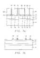
- FIG. 3 bshows power and ground distribution lines that are below a layer of passivation and power and ground distribution lines that are above a layer of passivation.
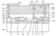
- passivation layer 18The most frequently used passivation layer in the present state of the art is plasma enhanced CVD (PECVD) oxide and nitride.
- PECVDplasma enhanced CVD
- a layer of approximately 0.5 ⁇ m PECVD oxidecan be deposited first followed by a layer of approximately 0.7 ⁇ m nitride.
- Passivation layer 18is very important because it protects the device wafer from moisture and foreign ion contamination.
- the positioning of this layer between the sub-micron process (of the integrated circuit) and the tens-micron process (of the interconnecting metallization structure)is of critical importance since it allows for a cheaper process that possibly has less stringent clean room requirements for the process of creating the interconnecting metallization structure.
- the method that is used to create the interconnect network that is shown in cross section in FIG. 4 acan be summarized as follows.
- a silicon substrate 40is provided, and active circuits 42 , 45 and 45 ′ have been created in the surface of the substrate 40 including an ESD circuit 45 , receiver 45 ′, driver 45 ′ and I/O circuit 45 ′.
- First layers 60 of dielectric of inorganic materialare deposited over the substrate 40 , and a fine-line interconnect network 61 is created in the layers 60 of dielectric, making contact with the active circuitry 42 , 45 and 45 ′.
Landscapes
- Engineering & Computer Science (AREA)
- Power Engineering (AREA)
- Physics & Mathematics (AREA)
- Computer Hardware Design (AREA)
- Microelectronics & Electronic Packaging (AREA)
- Condensed Matter Physics & Semiconductors (AREA)
- General Physics & Mathematics (AREA)
- Geometry (AREA)
- Manufacturing & Machinery (AREA)
- Internal Circuitry In Semiconductor Integrated Circuit Devices (AREA)
- Semiconductor Integrated Circuits (AREA)
- Formation Of Insulating Films (AREA)
Abstract
Description
Claims (20)
Priority Applications (1)
| Application Number | Priority Date | Filing Date | Title |
|---|---|---|---|
| US11/927,721US7534718B2 (en) | 2000-10-18 | 2007-10-30 | Post passivation interconnection schemes on top of IC chips |
Applications Claiming Priority (5)
| Application Number | Priority Date | Filing Date | Title |
|---|---|---|---|
| US09/691,497US6495442B1 (en) | 2000-10-18 | 2000-10-18 | Post passivation interconnection schemes on top of the IC chips |
| US10/278,106US6734563B2 (en) | 2000-10-18 | 2002-10-22 | Post passivation interconnection schemes on top of the IC chips |
| US10/653,628US7443033B2 (en) | 1998-12-21 | 2003-09-02 | Post passivation interconnection schemes on top of the IC chips |
| US11/273,071US7405150B2 (en) | 2000-10-18 | 2005-11-14 | Post passivation interconnection schemes on top of the IC chips |
| US11/927,721US7534718B2 (en) | 2000-10-18 | 2007-10-30 | Post passivation interconnection schemes on top of IC chips |
Related Parent Applications (1)
| Application Number | Title | Priority Date | Filing Date |
|---|---|---|---|
| US11/273,071ContinuationUS7405150B2 (en) | 2000-10-18 | 2005-11-14 | Post passivation interconnection schemes on top of the IC chips |
Publications (2)
| Publication Number | Publication Date |
|---|---|
| US20080085597A1 US20080085597A1 (en) | 2008-04-10 |
| US7534718B2true US7534718B2 (en) | 2009-05-19 |
Family
ID=24776761
Family Applications (37)
| Application Number | Title | Priority Date | Filing Date |
|---|---|---|---|
| US09/691,497Expired - LifetimeUS6495442B1 (en) | 1998-12-21 | 2000-10-18 | Post passivation interconnection schemes on top of the IC chips |
| US10/004,027CeasedUS6605528B1 (en) | 2000-10-18 | 2001-10-24 | Post passivation metal scheme for high-performance integrated circuit devices |
| US09/998,862Expired - LifetimeUS6649509B1 (en) | 1998-12-21 | 2001-10-24 | Post passivation metal scheme for high-performance integrated circuit devices |
| US10/278,106Expired - LifetimeUS6734563B2 (en) | 1998-12-21 | 2002-10-22 | Post passivation interconnection schemes on top of the IC chips |
| US10/653,628Expired - Fee RelatedUS7443033B2 (en) | 1998-12-21 | 2003-09-02 | Post passivation interconnection schemes on top of the IC chips |
| US11/273,447Expired - LifetimeUS7351650B2 (en) | 2000-10-18 | 2005-11-14 | Post passivation interconnection schemes on top of the IC chips |
| US11/273,071Expired - LifetimeUS7405150B2 (en) | 2000-10-18 | 2005-11-14 | Post passivation interconnection schemes on top of the IC chips |
| US11/273,085Expired - LifetimeUS7276422B2 (en) | 2000-10-18 | 2005-11-14 | Post passivation interconnection schemes on top of the IC chips |
| US11/273,105Expired - LifetimeUS7265047B2 (en) | 2000-10-18 | 2005-11-14 | Post passivation interconnection schemes on top of the IC chips |
| US11/518,595Expired - LifetimeUSRE43674E1 (en) | 2000-10-18 | 2006-09-08 | Post passivation metal scheme for high-performance integrated circuit devices |
| US11/854,559AbandonedUS20080067694A1 (en) | 2000-10-18 | 2007-09-13 | Post passivation interconnection schemes on top of IC chip |
| US11/854,561Expired - Fee RelatedUS7919865B2 (en) | 2000-10-18 | 2007-09-13 | Post passivation interconnection schemes on top of IC chip |
| US11/854,552Expired - Fee RelatedUS8004088B2 (en) | 2000-10-18 | 2007-09-13 | Post passivation interconnection schemes on top of IC chip |
| US11/854,555Expired - LifetimeUS7462938B2 (en) | 2000-10-18 | 2007-09-13 | Post passivation interconnection schemes on top of IC chip |
| US11/854,556AbandonedUS20080067693A1 (en) | 2000-10-18 | 2007-09-13 | Post passivation interconnection schemes on top of IC chip |
| US11/854,562Expired - Fee RelatedUS8461686B2 (en) | 2000-10-18 | 2007-09-13 | Post passivation interconnection schemes on top of IC chip |
| US11/856,080Expired - Fee RelatedUS7915161B2 (en) | 2000-10-18 | 2007-09-17 | Post passivation interconnection schemes on top of IC chip |
| US11/856,087Expired - Fee RelatedUS7923366B2 (en) | 2000-10-18 | 2007-09-17 | Post passivation interconnection schemes on top of IC chip |
| US11/856,077Expired - Fee RelatedUS7459791B2 (en) | 2000-10-18 | 2007-09-17 | Post passivation interconnection schemes on top of IC chip |
| US11/856,072Expired - LifetimeUS7382052B2 (en) | 2000-10-18 | 2007-09-17 | Post passivation interconnection schemes on top of IC chip |
| US11/856,082Expired - Fee RelatedUS7892965B2 (en) | 2000-10-18 | 2007-09-17 | Post passivation interconnection schemes on top of IC chip |
| US11/856,078Expired - LifetimeUS7466007B2 (en) | 2000-10-18 | 2007-09-17 | Post passivation interconnection schemes on top of IC chip |
| US11/856,083Expired - Fee RelatedUS7524759B2 (en) | 2000-10-18 | 2007-09-17 | Post passivation interconnection schemes on top of IC chip |
| US11/856,074Expired - Fee RelatedUS8492900B2 (en) | 2000-10-18 | 2007-09-17 | Post passivation interconnection schemes on top of IC chip |
| US11/856,073Expired - Fee RelatedUS8482127B2 (en) | 2000-10-18 | 2007-09-17 | Post passivation interconnection schemes on top of IC chip |
| US11/856,075Expired - LifetimeUS7439626B2 (en) | 2000-10-18 | 2007-09-17 | Post passivation interconnection schemes on top of IC chip |
| US11/856,076Expired - Fee RelatedUS8188603B2 (en) | 2000-10-18 | 2007-09-17 | Post passivation interconnection schemes on top of IC chip |
| US11/856,088Expired - Fee RelatedUS8435883B2 (en) | 2000-10-18 | 2007-09-17 | Post passivation interconnection schemes on top of IC chips |
| US11/856,081Expired - LifetimeUS7446035B2 (en) | 2000-10-18 | 2007-09-17 | Post passivation interconnection schemes on top of IC chips |
| US11/858,905Expired - LifetimeUS7443034B2 (en) | 2000-10-18 | 2007-09-21 | Post passivation interconnection schemes on top of the IC chips |
| US11/858,904Expired - LifetimeUS7419900B2 (en) | 2000-10-18 | 2007-09-21 | Post passivation interconnection schemes on top of the IC chips |
| US11/861,299Expired - LifetimeUS7479450B2 (en) | 2000-10-18 | 2007-09-26 | Post passivation interconnection schemes on top of the IC chips |
| US11/861,295Expired - LifetimeUS7439627B2 (en) | 2000-10-18 | 2007-09-26 | Post passivation interconnection schemes on top of the IC chips |
| US11/906,840Expired - Fee RelatedUS7902067B2 (en) | 2000-10-18 | 2007-10-04 | Post passivation interconnection schemes on top of the IC chips |
| US11/906,833Expired - LifetimeUS7449752B2 (en) | 2000-10-18 | 2007-10-04 | Post passivation interconnection schemes on top of the IC chips |
| US11/927,719Expired - LifetimeUS7446031B2 (en) | 2000-10-18 | 2007-10-30 | Post passivation interconnection schemes on top of IC chips |
| US11/927,721Expired - Fee RelatedUS7534718B2 (en) | 2000-10-18 | 2007-10-30 | Post passivation interconnection schemes on top of IC chips |
Family Applications Before (36)
| Application Number | Title | Priority Date | Filing Date |
|---|---|---|---|
| US09/691,497Expired - LifetimeUS6495442B1 (en) | 1998-12-21 | 2000-10-18 | Post passivation interconnection schemes on top of the IC chips |
| US10/004,027CeasedUS6605528B1 (en) | 2000-10-18 | 2001-10-24 | Post passivation metal scheme for high-performance integrated circuit devices |
| US09/998,862Expired - LifetimeUS6649509B1 (en) | 1998-12-21 | 2001-10-24 | Post passivation metal scheme for high-performance integrated circuit devices |
| US10/278,106Expired - LifetimeUS6734563B2 (en) | 1998-12-21 | 2002-10-22 | Post passivation interconnection schemes on top of the IC chips |
| US10/653,628Expired - Fee RelatedUS7443033B2 (en) | 1998-12-21 | 2003-09-02 | Post passivation interconnection schemes on top of the IC chips |
| US11/273,447Expired - LifetimeUS7351650B2 (en) | 2000-10-18 | 2005-11-14 | Post passivation interconnection schemes on top of the IC chips |
| US11/273,071Expired - LifetimeUS7405150B2 (en) | 2000-10-18 | 2005-11-14 | Post passivation interconnection schemes on top of the IC chips |
| US11/273,085Expired - LifetimeUS7276422B2 (en) | 2000-10-18 | 2005-11-14 | Post passivation interconnection schemes on top of the IC chips |
| US11/273,105Expired - LifetimeUS7265047B2 (en) | 2000-10-18 | 2005-11-14 | Post passivation interconnection schemes on top of the IC chips |
| US11/518,595Expired - LifetimeUSRE43674E1 (en) | 2000-10-18 | 2006-09-08 | Post passivation metal scheme for high-performance integrated circuit devices |
| US11/854,559AbandonedUS20080067694A1 (en) | 2000-10-18 | 2007-09-13 | Post passivation interconnection schemes on top of IC chip |
| US11/854,561Expired - Fee RelatedUS7919865B2 (en) | 2000-10-18 | 2007-09-13 | Post passivation interconnection schemes on top of IC chip |
| US11/854,552Expired - Fee RelatedUS8004088B2 (en) | 2000-10-18 | 2007-09-13 | Post passivation interconnection schemes on top of IC chip |
| US11/854,555Expired - LifetimeUS7462938B2 (en) | 2000-10-18 | 2007-09-13 | Post passivation interconnection schemes on top of IC chip |
| US11/854,556AbandonedUS20080067693A1 (en) | 2000-10-18 | 2007-09-13 | Post passivation interconnection schemes on top of IC chip |
| US11/854,562Expired - Fee RelatedUS8461686B2 (en) | 2000-10-18 | 2007-09-13 | Post passivation interconnection schemes on top of IC chip |
| US11/856,080Expired - Fee RelatedUS7915161B2 (en) | 2000-10-18 | 2007-09-17 | Post passivation interconnection schemes on top of IC chip |
| US11/856,087Expired - Fee RelatedUS7923366B2 (en) | 2000-10-18 | 2007-09-17 | Post passivation interconnection schemes on top of IC chip |
| US11/856,077Expired - Fee RelatedUS7459791B2 (en) | 2000-10-18 | 2007-09-17 | Post passivation interconnection schemes on top of IC chip |
| US11/856,072Expired - LifetimeUS7382052B2 (en) | 2000-10-18 | 2007-09-17 | Post passivation interconnection schemes on top of IC chip |
| US11/856,082Expired - Fee RelatedUS7892965B2 (en) | 2000-10-18 | 2007-09-17 | Post passivation interconnection schemes on top of IC chip |
| US11/856,078Expired - LifetimeUS7466007B2 (en) | 2000-10-18 | 2007-09-17 | Post passivation interconnection schemes on top of IC chip |
| US11/856,083Expired - Fee RelatedUS7524759B2 (en) | 2000-10-18 | 2007-09-17 | Post passivation interconnection schemes on top of IC chip |
| US11/856,074Expired - Fee RelatedUS8492900B2 (en) | 2000-10-18 | 2007-09-17 | Post passivation interconnection schemes on top of IC chip |
| US11/856,073Expired - Fee RelatedUS8482127B2 (en) | 2000-10-18 | 2007-09-17 | Post passivation interconnection schemes on top of IC chip |
| US11/856,075Expired - LifetimeUS7439626B2 (en) | 2000-10-18 | 2007-09-17 | Post passivation interconnection schemes on top of IC chip |
| US11/856,076Expired - Fee RelatedUS8188603B2 (en) | 2000-10-18 | 2007-09-17 | Post passivation interconnection schemes on top of IC chip |
| US11/856,088Expired - Fee RelatedUS8435883B2 (en) | 2000-10-18 | 2007-09-17 | Post passivation interconnection schemes on top of IC chips |
| US11/856,081Expired - LifetimeUS7446035B2 (en) | 2000-10-18 | 2007-09-17 | Post passivation interconnection schemes on top of IC chips |
| US11/858,905Expired - LifetimeUS7443034B2 (en) | 2000-10-18 | 2007-09-21 | Post passivation interconnection schemes on top of the IC chips |
| US11/858,904Expired - LifetimeUS7419900B2 (en) | 2000-10-18 | 2007-09-21 | Post passivation interconnection schemes on top of the IC chips |
| US11/861,299Expired - LifetimeUS7479450B2 (en) | 2000-10-18 | 2007-09-26 | Post passivation interconnection schemes on top of the IC chips |
| US11/861,295Expired - LifetimeUS7439627B2 (en) | 2000-10-18 | 2007-09-26 | Post passivation interconnection schemes on top of the IC chips |
| US11/906,840Expired - Fee RelatedUS7902067B2 (en) | 2000-10-18 | 2007-10-04 | Post passivation interconnection schemes on top of the IC chips |
| US11/906,833Expired - LifetimeUS7449752B2 (en) | 2000-10-18 | 2007-10-04 | Post passivation interconnection schemes on top of the IC chips |
| US11/927,719Expired - LifetimeUS7446031B2 (en) | 2000-10-18 | 2007-10-30 | Post passivation interconnection schemes on top of IC chips |
Country Status (5)
| Country | Link |
|---|---|
| US (37) | US6495442B1 (en) |
| EP (2) | EP2365524B1 (en) |
| DE (1) | DE60149714C5 (en) |
| ES (1) | ES2741876T3 (en) |
| SG (4) | SG135967A1 (en) |
Cited By (2)
| Publication number | Priority date | Publication date | Assignee | Title |
|---|---|---|---|---|
| US20080067686A1 (en)* | 2000-10-18 | 2008-03-20 | Megica Corporation | Post passivation interconnection schemes on top of IC chip |
| US20090325343A1 (en)* | 2003-06-24 | 2009-12-31 | Sang-Yun Lee | Bonded semiconductor structure and method of fabricating the same |
Families Citing this family (113)
| Publication number | Priority date | Publication date | Assignee | Title |
|---|---|---|---|---|
| US6762115B2 (en)* | 1998-12-21 | 2004-07-13 | Megic Corporation | Chip structure and process for forming the same |
| US7381642B2 (en)* | 2004-09-23 | 2008-06-03 | Megica Corporation | Top layers of metal for integrated circuits |
| US8021976B2 (en) | 2002-10-15 | 2011-09-20 | Megica Corporation | Method of wire bonding over active area of a semiconductor circuit |
| US6936531B2 (en) | 1998-12-21 | 2005-08-30 | Megic Corporation | Process of fabricating a chip structure |
| US7531417B2 (en)* | 1998-12-21 | 2009-05-12 | Megica Corporation | High performance system-on-chip passive device using post passivation process |
| US6869870B2 (en) | 1998-12-21 | 2005-03-22 | Megic Corporation | High performance system-on-chip discrete components using post passivation process |
| US8421158B2 (en)* | 1998-12-21 | 2013-04-16 | Megica Corporation | Chip structure with a passive device and method for forming the same |
| US6965165B2 (en) | 1998-12-21 | 2005-11-15 | Mou-Shiung Lin | Top layers of metal for high performance IC's |
| US7405149B1 (en) | 1998-12-21 | 2008-07-29 | Megica Corporation | Post passivation method for semiconductor chip or wafer |
| US6756295B2 (en)* | 1998-12-21 | 2004-06-29 | Megic Corporation | Chip structure and process for forming the same |
| US6303423B1 (en) | 1998-12-21 | 2001-10-16 | Megic Corporation | Method for forming high performance system-on-chip using post passivation process |
| US8178435B2 (en)* | 1998-12-21 | 2012-05-15 | Megica Corporation | High performance system-on-chip inductor using post passivation process |
| US7230340B2 (en)* | 2000-10-18 | 2007-06-12 | Megica Corporation | Post passivation interconnection schemes on top of the IC chips |
| US6979908B1 (en)* | 2000-01-11 | 2005-12-27 | Texas Instruments Incorporated | Input/output architecture for integrated circuits with efficient positioning of integrated circuit elements |
| US7271489B2 (en) | 2003-10-15 | 2007-09-18 | Megica Corporation | Post passivation interconnection schemes on top of the IC chips |
| US7372161B2 (en)* | 2000-10-18 | 2008-05-13 | Megica Corporation | Post passivation interconnection schemes on top of the IC chips |
| DE10231385B4 (en)* | 2001-07-10 | 2007-02-22 | Samsung Electronics Co., Ltd., Suwon | Semiconductor chip with bond pads and associated multi-chip package |
| US6759275B1 (en) | 2001-09-04 | 2004-07-06 | Megic Corporation | Method for making high-performance RF integrated circuits |
| US6798073B2 (en)* | 2001-12-13 | 2004-09-28 | Megic Corporation | Chip structure and process for forming the same |
| US7932603B2 (en) | 2001-12-13 | 2011-04-26 | Megica Corporation | Chip structure and process for forming the same |
| US6614091B1 (en)* | 2002-03-13 | 2003-09-02 | Motorola, Inc. | Semiconductor device having a wire bond pad and method therefor |
| US6730540B2 (en)* | 2002-04-18 | 2004-05-04 | Tru-Si Technologies, Inc. | Clock distribution networks and conductive lines in semiconductor integrated circuits |
| US7288845B2 (en)* | 2002-10-15 | 2007-10-30 | Marvell Semiconductor, Inc. | Fabrication of wire bond pads over underlying active devices, passive devices and/or dielectric layers in integrated circuits |
| DE10251530B4 (en)* | 2002-11-04 | 2005-03-03 | Infineon Technologies Ag | Stack arrangement of a memory module |
| DE10251527B4 (en)* | 2002-11-04 | 2007-01-25 | Infineon Technologies Ag | Method for producing a stack arrangement of a memory module |
| US6906386B2 (en)* | 2002-12-20 | 2005-06-14 | Advanced Analogic Technologies, Inc. | Testable electrostatic discharge protection circuits |
| US8368150B2 (en)* | 2003-03-17 | 2013-02-05 | Megica Corporation | High performance IC chip having discrete decoupling capacitors attached to its IC surface |
| US6888248B2 (en)* | 2003-03-26 | 2005-05-03 | Taiwan Semiconductor Manufacturing Co., Ltd | Extended length metal line for improved ESD performance |
| JP3858849B2 (en)* | 2003-04-16 | 2006-12-20 | ソニー株式会社 | Semiconductor device and manufacturing method thereof |
| US7319277B2 (en)* | 2003-05-08 | 2008-01-15 | Megica Corporation | Chip structure with redistribution traces |
| TWI236763B (en)* | 2003-05-27 | 2005-07-21 | Megic Corp | High performance system-on-chip inductor using post passivation process |
| US7470997B2 (en)* | 2003-07-23 | 2008-12-30 | Megica Corporation | Wirebond pad for semiconductor chip or wafer |
| US7026233B2 (en)* | 2003-08-06 | 2006-04-11 | Taiwan Semiconductor Manufacturing Company, Ltd. | Method for reducing defects in post passivation interconnect process |
| DE10337569B4 (en)* | 2003-08-14 | 2008-12-11 | Infineon Technologies Ag | Integrated connection arrangement and manufacturing method |
| US20070178710A1 (en)* | 2003-08-18 | 2007-08-02 | 3M Innovative Properties Company | Method for sealing thin film transistors |
| US7459790B2 (en)* | 2003-10-15 | 2008-12-02 | Megica Corporation | Post passivation interconnection schemes on top of the IC chips |
| US7394161B2 (en)* | 2003-12-08 | 2008-07-01 | Megica Corporation | Chip structure with pads having bumps or wirebonded wires formed thereover or used to be tested thereto |
| JP2005236107A (en)* | 2004-02-20 | 2005-09-02 | Toshiba Corp | Upper layer metal power standard cell, area compression device and circuit optimization device |
| US7422930B2 (en)* | 2004-03-02 | 2008-09-09 | Infineon Technologies Ag | Integrated circuit with re-route layer and stacked die assembly |
| JP2005303258A (en)* | 2004-03-16 | 2005-10-27 | Fujikura Ltd | Device and manufacturing method thereof |
| TWI331370B (en)* | 2004-06-18 | 2010-10-01 | Megica Corp | Connection between two circuitry components |
| US7465654B2 (en)* | 2004-07-09 | 2008-12-16 | Megica Corporation | Structure of gold bumps and gold conductors on one IC die and methods of manufacturing the structures |
| US8022544B2 (en) | 2004-07-09 | 2011-09-20 | Megica Corporation | Chip structure |
| TWI283443B (en) | 2004-07-16 | 2007-07-01 | Megica Corp | Post-passivation process and process of forming a polymer layer on the chip |
| US7706324B2 (en)* | 2004-07-19 | 2010-04-27 | Qualcomm Incorporated | On-demand reverse-link pilot transmission |
| NO321381B1 (en)* | 2004-07-22 | 2006-05-02 | Thin Film Electronics Asa | Electrical wire connection and associated contact device as well as process for their manufacture |
| US8552559B2 (en)* | 2004-07-29 | 2013-10-08 | Megica Corporation | Very thick metal interconnection scheme in IC chips |
| US7452803B2 (en)* | 2004-08-12 | 2008-11-18 | Megica Corporation | Method for fabricating chip structure |
| US7659628B2 (en)* | 2004-08-13 | 2010-02-09 | Imec | Contact structure comprising semiconductor and metal islands |
| US7355282B2 (en)* | 2004-09-09 | 2008-04-08 | Megica Corporation | Post passivation interconnection process and structures |
| US7423346B2 (en)* | 2004-09-09 | 2008-09-09 | Megica Corporation | Post passivation interconnection process and structures |
| US8008775B2 (en)* | 2004-09-09 | 2011-08-30 | Megica Corporation | Post passivation interconnection structures |
| US7521805B2 (en)* | 2004-10-12 | 2009-04-21 | Megica Corp. | Post passivation interconnection schemes on top of the IC chips |
| KR100594326B1 (en)* | 2005-03-22 | 2006-06-30 | 삼성전자주식회사 | Non-volatile memory device for 2-bit operation and manufacturing method thereof |
| US8384189B2 (en) | 2005-03-29 | 2013-02-26 | Megica Corporation | High performance system-on-chip using post passivation process |
| US7468545B2 (en)* | 2005-05-06 | 2008-12-23 | Megica Corporation | Post passivation structure for a semiconductor device and packaging process for same |
| TWI312169B (en)* | 2005-05-25 | 2009-07-11 | Megica Corporatio | Chip structure and process for forming the same |
| US7582556B2 (en)* | 2005-06-24 | 2009-09-01 | Megica Corporation | Circuitry component and method for forming the same |
| CN1901162B (en)* | 2005-07-22 | 2011-04-20 | 米辑电子股份有限公司 | Method for manufacturing circuit assembly by continuous electroplating and circuit assembly structure |
| US7776739B2 (en)* | 2005-09-09 | 2010-08-17 | Analog Devices, Inc. | Semiconductor device interconnection contact and fabrication method |
| US7473999B2 (en) | 2005-09-23 | 2009-01-06 | Megica Corporation | Semiconductor chip and process for forming the same |
| US7990037B2 (en)* | 2005-11-28 | 2011-08-02 | Megica Corporation | Carbon nanotube circuit component structure |
| US20070194451A1 (en)* | 2006-02-22 | 2007-08-23 | Chih-Hung Wu | Apparatus for integrated input/output circuit and verification method thereof |
| US8836146B2 (en)* | 2006-03-02 | 2014-09-16 | Qualcomm Incorporated | Chip package and method for fabricating the same |
| US8420520B2 (en)* | 2006-05-18 | 2013-04-16 | Megica Corporation | Non-cyanide gold electroplating for fine-line gold traces and gold pads |
| US8022552B2 (en)* | 2006-06-27 | 2011-09-20 | Megica Corporation | Integrated circuit and method for fabricating the same |
| US8421227B2 (en) | 2006-06-28 | 2013-04-16 | Megica Corporation | Semiconductor chip structure |
| US7928567B2 (en)* | 2006-06-30 | 2011-04-19 | Nxp B.V. | Power supply network |
| US7960825B2 (en)* | 2006-09-06 | 2011-06-14 | Megica Corporation | Chip package and method for fabricating the same |
| TWI370515B (en) | 2006-09-29 | 2012-08-11 | Megica Corp | Circuit component |
| US7964963B2 (en)* | 2006-10-05 | 2011-06-21 | Nec Corporation | Semiconductor package and method for manufacturing semiconductor package |
| DE102006058010B9 (en)* | 2006-12-08 | 2009-06-10 | Infineon Technologies Ag | Semiconductor device with cavity structure and manufacturing method |
| US8749021B2 (en)* | 2006-12-26 | 2014-06-10 | Megit Acquisition Corp. | Voltage regulator integrated with semiconductor chip |
| US7608538B2 (en)* | 2007-01-05 | 2009-10-27 | International Business Machines Corporation | Formation of vertical devices by electroplating |
| US8304813B2 (en)* | 2007-01-08 | 2012-11-06 | SanDisk Technologies, Inc. | Connection between an I/O region and the core region of an integrated circuit |
| US8193636B2 (en) | 2007-03-13 | 2012-06-05 | Megica Corporation | Chip assembly with interconnection by metal bump |
| US7964961B2 (en)* | 2007-04-12 | 2011-06-21 | Megica Corporation | Chip package |
| KR100873019B1 (en)* | 2007-07-13 | 2008-12-10 | 주식회사 하이닉스반도체 | Bonding pad to prevent peeling and forming method thereof |
| US7843064B2 (en)* | 2007-12-21 | 2010-11-30 | Taiwan Semiconductor Manufacturing Company, Ltd. | Structure and process for the formation of TSVs |
| US8440903B1 (en) | 2008-02-21 | 2013-05-14 | Stion Corporation | Method and structure for forming module using a powder coating and thermal treatment process |
| EP2260430A2 (en)* | 2008-02-22 | 2010-12-15 | Uniloc Usa, Inc. | License auditing for distributed applications |
| EP2311233A1 (en)* | 2008-05-21 | 2011-04-20 | Uniloc Usa, Inc. | Device and method for secured communication |
| US7939454B1 (en) | 2008-05-31 | 2011-05-10 | Stion Corporation | Module and lamination process for multijunction cells |
| US8080862B2 (en) | 2008-09-09 | 2011-12-20 | Qualcomm Incorporate | Systems and methods for enabling ESD protection on 3-D stacked devices |
| JP2010135391A (en)* | 2008-12-02 | 2010-06-17 | Seiko Epson Corp | Semiconductor device and method for manufacturing the same |
| CN102265716B (en) | 2008-12-26 | 2015-04-01 | 高通股份有限公司 | Chip packaging with power management integrated circuits and related technologies |
| KR101307490B1 (en) | 2009-03-30 | 2013-12-11 | 메기가 코포레이션 | Integrated circuit chip using top post-passivation technology and bottom structure technology |
| GB0906750D0 (en)* | 2009-04-18 | 2009-06-03 | Nokia Corp | A voltage suppressor component |
| US20100325719A1 (en)* | 2009-06-19 | 2010-12-23 | Craig Stephen Etchegoyen | System and Method for Redundancy in a Communication Network |
| US20100325149A1 (en)* | 2009-06-22 | 2010-12-23 | Craig Stephen Etchegoyen | System and Method for Auditing Software Usage |
| US20100325051A1 (en)* | 2009-06-22 | 2010-12-23 | Craig Stephen Etchegoyen | System and Method for Piracy Reduction in Software Activation |
| US20100325150A1 (en)* | 2009-06-22 | 2010-12-23 | Joseph Martin Mordetsky | System and Method for Tracking Application Usage |
| US20100325703A1 (en)* | 2009-06-23 | 2010-12-23 | Craig Stephen Etchegoyen | System and Method for Secured Communications by Embedded Platforms |
| KR101169531B1 (en)* | 2009-07-03 | 2012-07-27 | 가부시키가이샤 테라미크로스 | Semiconductor construct and manufacturing method thereof as well as semiconductor device and manufacturing method thereof |
| US20110021147A1 (en)* | 2009-07-21 | 2011-01-27 | Tout Walid R | System and method for determining connectivity status of short range wireless devices |
| TWM383199U (en)* | 2009-09-17 | 2010-06-21 | Mao Bang Electronic Co Ltd | Chip stacking assembly |
| WO2011033599A1 (en)* | 2009-09-21 | 2011-03-24 | 株式会社 東芝 | Semiconductor device |
| US8569887B2 (en)* | 2009-11-05 | 2013-10-29 | Taiwan Semiconductor Manufacturing Company, Ltd. | Post passivation interconnect with oxidation prevention layer |
| TWI512917B (en)* | 2011-01-03 | 2015-12-11 | Chipbond Technology Corp | Process of forming an anti-oxidant metal layer on an electronic device |
| US8642460B2 (en)* | 2011-06-08 | 2014-02-04 | International Business Machines Corporation | Semiconductor switching device and method of making the same |
| US9117677B2 (en)* | 2011-10-13 | 2015-08-25 | Taiwan Semiconductor Manufacturing Company, Ltd. | Semiconductor integrated circuit having a resistor and method of forming the same |
| US8618607B1 (en)* | 2012-07-02 | 2013-12-31 | Globalfoundries Inc. | Semiconductor devices formed on a continuous active region with an isolating conductive structure positioned between such semiconductor devices, and methods of making same |
| US9646899B2 (en)* | 2012-09-13 | 2017-05-09 | Micron Technology, Inc. | Interconnect assemblies with probed bond pads |
| US8994173B2 (en) | 2013-06-26 | 2015-03-31 | International Business Machines Corporation | Solder bump connection and method of making |
| US9006584B2 (en) | 2013-08-06 | 2015-04-14 | Texas Instruments Incorporated | High voltage polymer dielectric capacitor isolation device |
| JP6238121B2 (en)* | 2013-10-01 | 2017-11-29 | ローム株式会社 | Semiconductor device |
| US9373576B2 (en)* | 2014-01-09 | 2016-06-21 | Broadcom Corporation | Flip chip pad geometry for an IC package substrate |
| US20180166419A1 (en)* | 2016-12-12 | 2018-06-14 | Nanya Technology Corporation | Semiconductor package |
| US10157867B1 (en)* | 2017-08-31 | 2018-12-18 | Taiwan Semiconductor Manufacturing Company, Ltd. | Interconnect structure and method |
| CN113496993B (en)* | 2020-04-01 | 2025-05-20 | 中芯国际集成电路制造(上海)有限公司 | Semiconductor structure and forming method thereof |
| CN111430329B (en)* | 2020-04-23 | 2021-07-27 | 合肥晶合集成电路股份有限公司 | Capacitive semiconductor element |
| KR20220022926A (en) | 2020-08-19 | 2022-03-02 | 삼성디스플레이 주식회사 | Display device |
| CN119447121A (en)* | 2024-11-11 | 2025-02-14 | 奇异摩尔(上海)集成电路设计有限公司 | A packaged chip and a manufacturing method thereof |
Citations (64)
| Publication number | Priority date | Publication date | Assignee | Title |
|---|---|---|---|---|
| US3030877A (en) | 1957-07-18 | 1962-04-24 | Sperry Rand Corp | Hay balers |
| US4423547A (en) | 1981-06-01 | 1984-01-03 | International Business Machines Corporation | Method for forming dense multilevel interconnection metallurgy for semiconductor devices |
| US4670091A (en) | 1984-08-23 | 1987-06-02 | Fairchild Semiconductor Corporation | Process for forming vias on integrated circuits |
| US5055907A (en) | 1989-01-25 | 1991-10-08 | Mosaic, Inc. | Extended integration semiconductor structure with wiring layers |
| US5083187A (en) | 1990-05-16 | 1992-01-21 | Texas Instruments Incorporated | Integrated circuit device having bumped power supply buses over active surface areas and method of manufacture thereof |
| US5106461A (en) | 1989-04-04 | 1992-04-21 | Massachusetts Institute Of Technology | High-density, multi-level interconnects, flex circuits, and tape for tab |
| US5108950A (en) | 1987-11-18 | 1992-04-28 | Casio Computer Co., Ltd. | Method for forming a bump electrode for a semiconductor device |
| US5212403A (en) | 1990-09-10 | 1993-05-18 | Hitachi, Ltd. | Integrated circuit device having an ic chip mounted on the wiring substrate and having suitable mutual connections between internal circuits |
| US5227012A (en) | 1990-04-24 | 1993-07-13 | Hightec Mg Ag | Method of manufacturing multi-layer thin film circuits containing integrated thin film resistors |
| US5300461A (en) | 1993-01-25 | 1994-04-05 | Intel Corporation | Process for fabricating sealed semiconductor chip using silicon nitride passivation film |
| US5384488A (en) | 1992-06-15 | 1995-01-24 | Texas Instruments Incorporated | Configuration and method for positioning semiconductor device bond pads using additional process layers |
| US5416356A (en) | 1993-09-03 | 1995-05-16 | Motorola, Inc. | Integrated circuit having passive circuit elements |
| US5468984A (en) | 1994-11-02 | 1995-11-21 | Texas Instruments Incorporated | ESD protection structure using LDMOS diodes with thick copper interconnect |
| US5478773A (en) | 1994-04-28 | 1995-12-26 | Motorola, Inc. | Method of making an electronic device having an integrated inductor |
| US5501006A (en) | 1993-09-22 | 1996-03-26 | Motorola, Inc. | Method for connection of signals to an integrated circuit |
| US5635767A (en) | 1995-06-02 | 1997-06-03 | Motorola, Inc. | Semiconductor device having built-in high frequency bypass capacitor |
| US5659201A (en) | 1995-06-05 | 1997-08-19 | Advanced Micro Devices, Inc. | High conductivity interconnection line |
| US5663108A (en) | 1996-06-13 | 1997-09-02 | Taiwan Semiconductor Manufacturing Company, Ltd. | Optimized metal pillar via process |
| US5686764A (en) | 1996-03-20 | 1997-11-11 | Lsi Logic Corporation | Flip chip package with reduced number of package layers |
| US5739560A (en) | 1994-09-22 | 1998-04-14 | Nippon Telegraph And Telephone Corporation | High frequency masterslice monolithic integrated circuit |
| US5789303A (en) | 1994-11-28 | 1998-08-04 | Northern Telecom Limited | Method of adding on chip capacitors to an integrated circuit |
| US5834844A (en) | 1995-03-24 | 1998-11-10 | Shinko Electric Industries Co., Ltd. | Semiconductor device having an element with circuit pattern thereon |
| US5929508A (en) | 1998-05-21 | 1999-07-27 | Harris Corp | Defect gettering by induced stress |
| US6020640A (en) | 1996-12-19 | 2000-02-01 | Texas Instruments Incorporated | Thick plated interconnect and associated auxillary interconnect |
| US6030877A (en) | 1997-10-06 | 2000-02-29 | Industrial Technology Research Institute | Electroless gold plating method for forming inductor structures |
| US6040604A (en) | 1997-07-21 | 2000-03-21 | Motorola, Inc. | Semiconductor component comprising an electrostatic-discharge protection device |
| JP2000216264A (en) | 1999-01-22 | 2000-08-04 | Mitsubishi Electric Corp | CMOS logic circuit element, semiconductor device, method of manufacturing the same, and semiconductor circuit design method used in the method of manufacturing the same |
| US6117782A (en) | 1999-04-22 | 2000-09-12 | Advanced Micro Devices, Inc. | Optimized trench/via profile for damascene filling |
| EP1039544A1 (en) | 1999-03-23 | 2000-09-27 | Memscap | Monolithic integrated circuit comprising an inductor and a method of fabricating the same |
| US6144100A (en)* | 1997-06-05 | 2000-11-07 | Texas Instruments Incorporated | Integrated circuit with bonding layer over active circuitry |
| US6146958A (en) | 1996-10-02 | 2000-11-14 | National Semiconductor Corporation | Methods for making VLSI capacitors and high Q VLSI inductors using metal-filled via plugs |
| US6187680B1 (en) | 1998-10-07 | 2001-02-13 | International Business Machines Corporation | Method/structure for creating aluminum wirebound pad on copper BEOL |
| US6200888B1 (en) | 1999-05-07 | 2001-03-13 | Shinko Electric Industries Co., Ltd. | Method of producing semiconductor device comprising insulation layer having improved resistance and semiconductor device produced thereby |
| US6229221B1 (en) | 1998-12-04 | 2001-05-08 | U.S. Philips Corporation | Integrated circuit device |
| US6232147B1 (en) | 1997-03-19 | 2001-05-15 | Fujitsu Limited | Method for manufacturing semiconductor device with pad structure |
| US6236101B1 (en) | 1997-11-05 | 2001-05-22 | Texas Instruments Incorporated | Metallization outside protective overcoat for improved capacitors and inductors |
| US6271127B1 (en) | 1999-06-10 | 2001-08-07 | Conexant Systems, Inc. | Method for dual damascene process using electron beam and ion implantation cure methods for low dielectric constant materials |
| US6294425B1 (en) | 1999-10-14 | 2001-09-25 | Samsung Electronics Co., Ltd. | Methods of forming integrated circuit capacitors by electroplating electrodes from seed layers |
| US6303423B1 (en) | 1998-12-21 | 2001-10-16 | Megic Corporation | Method for forming high performance system-on-chip using post passivation process |
| US20020017730A1 (en) | 2000-08-11 | 2002-02-14 | Integrated Electronics & Packaging | Semiconductor device |
| US6383916B1 (en) | 1998-12-21 | 2002-05-07 | M. S. Lin | Top layers of metal for high performance IC's |
| US6416958B2 (en) | 1998-08-28 | 2002-07-09 | Dendreon Corporation | Selective apoptosis of neoplastic cells by an HLA-DR specific monoclonal antibody |
| US20020109232A1 (en) | 1998-12-21 | 2002-08-15 | Mou-Shiung Lin | Chip structure and process for forming the same |
| US20020115282A1 (en) | 1998-12-21 | 2002-08-22 | Mou-Shiung Lin | Chip structure and process for forming the same |
| US6465879B1 (en) | 1999-10-19 | 2002-10-15 | Citizen Watch Co., Ltd. | Structure for mounting semiconductor device, method of mounting same, semiconductor device, and method of fabricating same |
| US6472745B1 (en) | 1999-01-18 | 2002-10-29 | Shinko Electric Industries Co., Ltd. | Semiconductor device |
| US20020158334A1 (en) | 2001-04-30 | 2002-10-31 | Intel Corporation | Microelectronic device having signal distribution functionality on an interfacial layer thereof |
| US6495442B1 (en) | 2000-10-18 | 2002-12-17 | Magic Corporation | Post passivation interconnection schemes on top of the IC chips |
| US6501169B1 (en) | 1999-11-29 | 2002-12-31 | Casio Computer Co., Ltd. | Semiconductor device which prevents leakage of noise generated in a circuit element forming area and which shields against external electromagnetic noise |
| US6544880B1 (en) | 1999-06-14 | 2003-04-08 | Micron Technology, Inc. | Method of improving copper interconnects of semiconductor devices for bonding |
| US6545354B1 (en) | 1999-02-15 | 2003-04-08 | Casio Computer Co., Ltd. | Semiconductor device having a barrier layer |
| US20030102551A1 (en) | 2000-07-13 | 2003-06-05 | Hidekazu Kikuchi | Semiconductor device and method for manufacturing |
| US6636139B2 (en) | 2001-09-10 | 2003-10-21 | Taiwan Semiconductor Manufacturing Company | Structure to reduce the degradation of the Q value of an inductor caused by via resistance |
| US6683380B2 (en) | 2000-07-07 | 2004-01-27 | Texas Instruments Incorporated | Integrated circuit with bonding layer over active circuitry |
| US20040089951A1 (en) | 2000-10-18 | 2004-05-13 | Megic Corporation | Post passivation interconnection schemes on top of the IC chips |
| US6759275B1 (en) | 2001-09-04 | 2004-07-06 | Megic Corporation | Method for making high-performance RF integrated circuits |
| US20040166659A1 (en) | 1998-12-21 | 2004-08-26 | Megic Corporation | Top layers of metal for high performance IC's |
| US6800555B2 (en) | 2000-03-24 | 2004-10-05 | Texas Instruments Incorporated | Wire bonding process for copper-metallized integrated circuits |
| US20050104177A1 (en) | 2000-10-18 | 2005-05-19 | Megic Corporation | Post passivation interconnection schemes on top of the IC chips |
| US20060049483A1 (en) | 2004-09-09 | 2006-03-09 | Megic Corporation | Post passivation interconnection process and structures |
| US20060049525A1 (en) | 2004-09-09 | 2006-03-09 | Megic Corporation | Post passivation interconnection process and structures |
| US20060049524A1 (en) | 2004-09-09 | 2006-03-09 | Megic Corporation | Post passivation interconnection process and structures |
| US20060063378A1 (en) | 2004-09-23 | 2006-03-23 | Megie Corporation | Top layers of metal for integrated circuits |
| US20060076687A1 (en) | 2003-10-15 | 2006-04-13 | Megic Corporation | Post passivation interconnection schemes on top of the IC chips |
Family Cites Families (153)
| Publication number | Priority date | Publication date | Assignee | Title |
|---|---|---|---|---|
| US608060A (en)* | 1898-07-26 | Edward j | ||
| GB1244013A (en) | 1967-10-13 | 1971-08-25 | Gen Electric | Fabrication of semiconductor devices |
| JPS5232234B2 (en)* | 1971-10-11 | 1977-08-19 | ||
| US3953625A (en)* | 1971-12-07 | 1976-04-27 | Horizons Incorporated | Process for making indicia bearing anodized article |
| JPS5851425B2 (en)* | 1975-08-22 | 1983-11-16 | 株式会社日立製作所 | Hand tie souchi |
| US4300184A (en) | 1979-07-11 | 1981-11-10 | Johnson Controls, Inc. | Conformal coating for electrical circuit assemblies |
| US4685998A (en) | 1984-03-22 | 1987-08-11 | Thomson Components - Mostek Corp. | Process of forming integrated circuits with contact pads in a standard array |
| US5111276A (en)* | 1985-03-19 | 1992-05-05 | National Semiconductor Corp. | Thick bus metallization interconnect structure to reduce bus area |
| NL8600021A (en) | 1986-01-08 | 1987-08-03 | Philips Nv | METHOD FOR MANUFACTURING A SEMICONDUCTOR DEVICE APPLYING METALIZATION TO A SEMICONDUCTOR BODY |
| KR900008647B1 (en)* | 1986-03-20 | 1990-11-26 | 후지쓰 가부시끼가이샤 | A method for manufacturing three demensional i.c. |
| US4753896A (en)* | 1986-11-21 | 1988-06-28 | Texas Instruments Incorporated | Sidewall channel stop process |
| JPH01214141A (en) | 1988-02-23 | 1989-08-28 | Nec Corp | Flip-chip type semiconductor device |
| US5061985A (en) | 1988-06-13 | 1991-10-29 | Hitachi, Ltd. | Semiconductor integrated circuit device and process for producing the same |
| US4927505A (en) | 1988-07-05 | 1990-05-22 | Motorola Inc. | Metallization scheme providing adhesion and barrier properties |
| US5719448A (en) | 1989-03-07 | 1998-02-17 | Seiko Epson Corporation | Bonding pad structures for semiconductor integrated circuits |
| DE68916784T2 (en) | 1989-04-20 | 1995-01-05 | Ibm | Integrated circuit pack. |
| US5244833A (en) | 1989-07-26 | 1993-09-14 | International Business Machines Corporation | Method for manufacturing an integrated circuit chip bump electrode using a polymer layer and a photoresist layer |
| FR2654366B1 (en)* | 1989-11-16 | 1992-02-14 | Sorapec | METHOD AND DEVICE FOR PASTING A PLATE-SHAPED ALVEOLAR STRUCTURE. |
| US5074947A (en) | 1989-12-18 | 1991-12-24 | Epoxy Technology, Inc. | Flip chip technology using electrically conductive polymers and dielectrics |
| US5226232A (en) | 1990-05-18 | 1993-07-13 | Hewlett-Packard Company | Method for forming a conductive pattern on an integrated circuit |
| US5130275A (en) | 1990-07-02 | 1992-07-14 | Digital Equipment Corp. | Post fabrication processing of semiconductor chips |
| US5145571A (en)* | 1990-08-03 | 1992-09-08 | Bipolar Integrated Technology, Inc. | Gold interconnect with sidewall-spacers |
| US5118369A (en)* | 1990-08-23 | 1992-06-02 | Colorcode Unlimited Corporation | Microlabelling system and process for making microlabels |
| FR2666190B1 (en) | 1990-08-24 | 1996-07-12 | Thomson Csf | METHOD AND DEVICE FOR HERMETIC ENCAPSULATION OF ELECTRONIC COMPONENTS. |
| US5223604A (en)* | 1991-06-25 | 1993-06-29 | S.P.I. Synthetic Peptides Incorporated | Pseudomonas exoenzyme s peptide composition and method |
| KR940007290B1 (en) | 1991-12-14 | 1994-08-12 | 현대전자산업 주식회사 | How to Form Wire Bonding Pads |
| US5336921A (en) | 1992-01-27 | 1994-08-09 | Motorola, Inc. | Vertical trench inductor |
| KR940001341A (en) | 1992-06-29 | 1994-01-11 | 디. 아이. 캐플란 | Instant connection for quick electrical access to electronic devices |
| US6274391B1 (en) | 1992-10-26 | 2001-08-14 | Texas Instruments Incorporated | HDI land grid array packaged device having electrical and optical interconnects |
| US5346738A (en)* | 1992-11-04 | 1994-09-13 | X-Cal Corporation | Identification label with micro-encapsulated etchant |
| KR970000424Y1 (en)* | 1992-12-07 | 1997-01-20 | 김해운 | Color code label for data classification |
| JPH06232379A (en) | 1993-02-01 | 1994-08-19 | Sharp Corp | Solid-state image pickup element |
| US5461333A (en) | 1993-03-15 | 1995-10-24 | At&T Ipm Corp. | Multi-chip modules having chip-to-chip interconnections with reduced signal voltage level and swing |
| US5641997A (en) | 1993-09-14 | 1997-06-24 | Kabushiki Kaisha Toshiba | Plastic-encapsulated semiconductor device |
| US6023103A (en) | 1994-11-15 | 2000-02-08 | Formfactor, Inc. | Chip-scale carrier for semiconductor devices including mounted spring contacts |
| JPH07201864A (en)* | 1993-12-28 | 1995-08-04 | Fujitsu Ltd | Method of forming bump electrodes |
| US5576680A (en) | 1994-03-01 | 1996-11-19 | Amer-Soi | Structure and fabrication process of inductors on semiconductor chip |
| US5644102A (en) | 1994-03-01 | 1997-07-01 | Lsi Logic Corporation | Integrated circuit packages with distinctive coloration |
| US6577148B1 (en) | 1994-08-31 | 2003-06-10 | Motorola, Inc. | Apparatus, method, and wafer used for testing integrated circuits formed on a product wafer |
| US5532512A (en) | 1994-10-03 | 1996-07-02 | General Electric Company | Direct stacked and flip chip power semiconductor device structures |
| US5892273A (en) | 1994-10-03 | 1999-04-06 | Kabushiki Kaisha Toshiba | Semiconductor package integral with semiconductor chip |
| US5629240A (en)* | 1994-12-09 | 1997-05-13 | Sun Microsystems, Inc. | Method for direct attachment of an on-chip bypass capacitor in an integrated circuit |
| US5665996A (en) | 1994-12-30 | 1997-09-09 | Siliconix Incorporated | Vertical power mosfet having thick metal layer to reduce distributed resistance |
| US5665989A (en) | 1995-01-03 | 1997-09-09 | Lsi Logic | Programmable microsystems in silicon |
| US5534465A (en)* | 1995-01-10 | 1996-07-09 | At&T Corp. | Method for making multichip circuits using active semiconductor substrates |
| US5731945A (en) | 1995-02-22 | 1998-03-24 | International Business Machines Corporation | Multichip semiconductor structures with consolidated circuitry and programmable ESD protection for input/output nodes |
| WO1996030933A2 (en) | 1995-03-20 | 1996-10-03 | Mcnc | Solder bump fabrication methods and structure including a titanium barrier layer |
| KR0177395B1 (en) | 1995-04-27 | 1999-05-15 | 문정환 | Chip mounted circuit board and method for manufacturing the same |
| US5541135A (en) | 1995-05-30 | 1996-07-30 | Motorola, Inc. | Method of fabricating a flip chip semiconductor device having an inductor |
| KR100327442B1 (en) | 1995-07-14 | 2002-06-29 | 구본준, 론 위라하디락사 | Bump Structure and Forming Method of Semiconductor Device |
| US5691248A (en) | 1995-07-26 | 1997-11-25 | International Business Machines Corporation | Methods for precise definition of integrated circuit chip edges |
| US5736792A (en) | 1995-08-30 | 1998-04-07 | Texas Instruments Incorporated | Method of protecting bond wires during molding and handling |
| US5569956A (en) | 1995-08-31 | 1996-10-29 | National Semiconductor Corporation | Interposer connecting leadframe and integrated circuit |
| US5656849A (en)* | 1995-09-22 | 1997-08-12 | International Business Machines Corporation | Two-level spiral inductor structure having a high inductance to area ratio |
| JPH09115829A (en)* | 1995-10-17 | 1997-05-02 | Nissan Motor Co Ltd | Semiconductor device having aluminum wiring and method for manufacturing the same |
| US5818748A (en) | 1995-11-21 | 1998-10-06 | International Business Machines Corporation | Chip function separation onto separate stacked chips |
| JP2739853B2 (en)* | 1995-11-28 | 1998-04-15 | 日本電気株式会社 | Semiconductor device manufacturing method and etching method |
| JP2814972B2 (en)* | 1995-12-18 | 1998-10-27 | 日本電気株式会社 | Method for manufacturing semiconductor device |
| US5869869A (en)* | 1996-01-31 | 1999-02-09 | Lsi Logic Corporation | Microelectronic device with thin film electrostatic discharge protection structure |
| TW357449B (en) | 1996-02-02 | 1999-05-01 | Taiwan Semiconductor Mfg Co Ltd | Electro-Static Discharge (ESD) protective circuit |
| US5851911A (en)* | 1996-03-07 | 1998-12-22 | Micron Technology, Inc. | Mask repattern process |
| US6022792A (en) | 1996-03-13 | 2000-02-08 | Seiko Instruments, Inc. | Semiconductor dicing and assembling method |
| US5792594A (en) | 1996-04-01 | 1998-08-11 | Motorola, Inc. | Metallization and termination process for an integrated circuit chip |
| KR0176202B1 (en)* | 1996-04-09 | 1999-04-15 | 김광호 | S.O.I transistor and its manufacturing method |
| US5953626A (en)* | 1996-06-05 | 1999-09-14 | Advanced Micro Devices, Inc. | Dissolvable dielectric method |
| US6429120B1 (en) | 2000-01-18 | 2002-08-06 | Micron Technology, Inc. | Methods and apparatus for making integrated-circuit wiring from copper, silver, gold, and other metals |
| WO1998003994A1 (en)* | 1996-07-18 | 1998-01-29 | Advanced Micro Devices, Inc. | Integrated circuit which uses an etch stop for producing staggered interconnect lines |
| US5883435A (en) | 1996-07-25 | 1999-03-16 | International Business Machines Corporation | Personalization structure for semiconductor devices |
| US5793272A (en) | 1996-08-23 | 1998-08-11 | International Business Machines Corporation | Integrated circuit toroidal inductor |
| JP3305211B2 (en) | 1996-09-10 | 2002-07-22 | 松下電器産業株式会社 | Semiconductor device and manufacturing method thereof |
| US5805043A (en)* | 1996-10-02 | 1998-09-08 | Itt Industries, Inc. | High Q compact inductors for monolithic integrated circuit applications |
| US5952726A (en) | 1996-11-12 | 1999-09-14 | Lsi Logic Corporation | Flip chip bump distribution on die |
| US5818110A (en) | 1996-11-22 | 1998-10-06 | International Business Machines Corporation | Integrated circuit chip wiring structure with crossover capability and method of manufacturing the same |
| US6025275A (en)* | 1996-12-19 | 2000-02-15 | Texas Instruments Incorporated | Method of forming improved thick plated copper interconnect and associated auxiliary metal interconnect |
| US5856217A (en)* | 1997-04-10 | 1999-01-05 | Hughes Electronics Corporation | Modulation-doped field-effect transistors and fabrication processes |
| TW396584B (en) | 1997-08-14 | 2000-07-01 | Taiwan Semiconductor Mfg | The producing method of the electrostatic discharge protective circuit in IC |
| JP3660799B2 (en) | 1997-09-08 | 2005-06-15 | 株式会社ルネサステクノロジ | Manufacturing method of semiconductor integrated circuit device |
| US6147857A (en)* | 1997-10-07 | 2000-11-14 | E. R. W. | Optional on chip power supply bypass capacitor |
| US6441487B2 (en)* | 1997-10-20 | 2002-08-27 | Flip Chip Technologies, L.L.C. | Chip scale package using large ductile solder balls |
| US6075290A (en) | 1998-02-26 | 2000-06-13 | National Semiconductor Corporation | Surface mount die: wafer level chip-scale package and process for making the same |
| JP3955386B2 (en) | 1998-04-09 | 2007-08-08 | 富士通株式会社 | Semiconductor device and manufacturing method thereof |
| US6008102A (en) | 1998-04-09 | 1999-12-28 | Motorola, Inc. | Method of forming a three-dimensional integrated inductor |
| US6008060A (en) | 1998-04-14 | 1999-12-28 | Etec Systems, Inc. | Detecting registration marks with a low energy electron beam |
| US6111301A (en)* | 1998-04-24 | 2000-08-29 | International Business Machines Corporation | Interconnection with integrated corrosion stop |
| AUPP344298A0 (en)* | 1998-05-12 | 1998-06-04 | Enviro-Mulch Pty Ltd | Method and apparatus for mulching waste |
| US6100337A (en)* | 1998-05-18 | 2000-08-08 | Shell Oil Company | Functionalized thermoplastic elastomer |
| US6391771B1 (en) | 1998-07-23 | 2002-05-21 | Applied Materials, Inc. | Integrated circuit interconnect lines having sidewall layers |
| US6077726A (en) | 1998-07-30 | 2000-06-20 | Motorola, Inc. | Method and apparatus for stress relief in solder bump formation on a semiconductor device |
| US6103552A (en) | 1998-08-10 | 2000-08-15 | Lin; Mou-Shiung | Wafer scale packaging scheme |
| US5994766A (en) | 1998-09-21 | 1999-11-30 | Vlsi Technology, Inc. | Flip chip circuit arrangement with redistribution layer that minimizes crosstalk |
| US6272736B1 (en) | 1998-11-13 | 2001-08-14 | United Microelectronics Corp. | Method for forming a thin-film resistor |
| JP2000183104A (en) | 1998-12-15 | 2000-06-30 | Texas Instr Inc <Ti> | System and method for bonding on an integrated circuit |
| SE514839C2 (en) | 1998-12-18 | 2001-04-30 | Volvo Ab | Motor vehicle |
| US6936531B2 (en) | 1998-12-21 | 2005-08-30 | Megic Corporation | Process of fabricating a chip structure |
| US6359328B1 (en) | 1998-12-31 | 2002-03-19 | Intel Corporation | Methods for making interconnects and diffusion barriers in integrated circuits |
| US6417094B1 (en)* | 1998-12-31 | 2002-07-09 | Newport Fab, Llc | Dual-damascene interconnect structures and methods of fabricating same |
| US6011314A (en) | 1999-02-01 | 2000-01-04 | Hewlett-Packard Company | Redistribution layer and under bump material structure for converting periphery conductive pads to an array of solder bumps |
| US6121092A (en) | 1999-02-02 | 2000-09-19 | Macronix International Co., Ltd. | Silicide blocking process to form non-silicided regions on MOS devices |
| US6159773A (en) | 1999-02-12 | 2000-12-12 | Lin; Mou-Shiung | Strain release contact system for integrated circuits |
| US6180426B1 (en)* | 1999-03-01 | 2001-01-30 | Mou-Shiung Lin | High performance sub-system design and assembly |
| JP3519632B2 (en)* | 1999-03-11 | 2004-04-19 | 株式会社東芝 | Method for manufacturing semiconductor device |
| US6140241A (en)* | 1999-03-18 | 2000-10-31 | Taiwan Semiconductor Manufacturing Company | Multi-step electrochemical copper deposition process with improved filling capability |
| JP4995364B2 (en) | 1999-03-25 | 2012-08-08 | セイコーインスツル株式会社 | Semiconductor integrated circuit device |
| US6031293A (en)* | 1999-04-26 | 2000-02-29 | United Microelectronics Corporation | Package-free bonding pad structure |
| US6300242B1 (en)* | 1999-04-28 | 2001-10-09 | Matsuhita Electronics Corporation | Semiconductor device and method of fabricating the same |
| US6539328B1 (en)* | 1999-04-30 | 2003-03-25 | Sigma Instruments, Inc. | Device and process for measurement and treatment of spinal mobility |
| US6306749B1 (en) | 1999-06-08 | 2001-10-23 | Winbond Electronics Corp | Bond pad with pad edge strengthening structure |
| US6214714B1 (en)* | 1999-06-25 | 2001-04-10 | Applied Materials, Inc. | Method of titanium/titanium nitride integration |
| US6617681B1 (en)* | 1999-06-28 | 2003-09-09 | Intel Corporation | Interposer and method of making same |
| JP3194917B2 (en) | 1999-08-10 | 2001-08-06 | トーワ株式会社 | Resin sealing method |
| JP3859403B2 (en) | 1999-09-22 | 2006-12-20 | 株式会社東芝 | Semiconductor device and manufacturing method thereof |
| KR100313706B1 (en)* | 1999-09-29 | 2001-11-26 | 윤종용 | Redistributed Wafer Level Chip Size Package And Method For Manufacturing The Same |
| KR100306842B1 (en)* | 1999-09-30 | 2001-11-02 | 윤종용 | Redistributed Wafer Level Chip Size Package Having Concave Pattern In Bump Pad And Method For Manufacturing The Same |
| US6410435B1 (en) | 1999-10-01 | 2002-06-25 | Agere Systems Guardian Corp. | Process for fabricating copper interconnect for ULSI integrated circuits |
| US6511901B1 (en)* | 1999-11-05 | 2003-01-28 | Atmel Corporation | Metal redistribution layer having solderable pads and wire bondable pads |
| US6117747A (en) | 1999-11-22 | 2000-09-12 | Chartered Semiconductor Manufacturing Ltd. | Integration of MOM capacitor into dual damascene process |
| US6803302B2 (en) | 1999-11-22 | 2004-10-12 | Freescale Semiconductor, Inc. | Method for forming a semiconductor device having a mechanically robust pad interface |
| JP2001161630A (en) | 1999-12-09 | 2001-06-19 | Olympus Optical Co Ltd | Endoscope |
| US6380555B1 (en)* | 1999-12-24 | 2002-04-30 | Micron Technology, Inc. | Bumped semiconductor component having test pads, and method and system for testing bumped semiconductor components |
| US6420262B1 (en)* | 2000-01-18 | 2002-07-16 | Micron Technology, Inc. | Structures and methods to enhance copper metallization |
| JP2001217242A (en) | 2000-02-03 | 2001-08-10 | Seiko Epson Corp | Semiconductor device and method of manufacturing the same |
| KR100350111B1 (en) | 2000-02-22 | 2002-08-23 | 삼성전자 주식회사 | Wiring of Semiconductor Device and Method for Manufacturing Thereof |
| TW441020B (en) | 2000-02-24 | 2001-06-16 | United Microelectronics Corp | Method for forming cap layer of self-aligned copper interconnect |
| US6620720B1 (en)* | 2000-04-10 | 2003-09-16 | Agere Systems Inc | Interconnections to copper IC's |
| US6578754B1 (en) | 2000-04-27 | 2003-06-17 | Advanpack Solutions Pte. Ltd. | Pillar connections for semiconductor chips and method of manufacture |
| US6362087B1 (en) | 2000-05-05 | 2002-03-26 | Aptos Corporation | Method for fabricating a microelectronic fabrication having formed therein a redistribution structure |
| US6300234B1 (en) | 2000-06-26 | 2001-10-09 | Motorola, Inc. | Process for forming an electrical device |
| TW523792B (en)* | 2000-09-07 | 2003-03-11 | Toshiba Corp | Semiconductor device and its manufacturing method |
| EP1198004A3 (en) | 2000-10-13 | 2003-10-01 | Texas Instruments Inc. | Semiconductor device having power distribution lines thereon |
| JP2002198374A (en) | 2000-10-16 | 2002-07-12 | Sharp Corp | Semiconductor device and method of manufacturing the same |
| TW577152B (en) | 2000-12-18 | 2004-02-21 | Hitachi Ltd | Semiconductor integrated circuit device |
| JPWO2002063681A1 (en) | 2001-02-08 | 2004-06-10 | 株式会社ルネサステクノロジ | Semiconductor integrated circuit device and method of manufacturing the same |
| US6653563B2 (en) | 2001-03-30 | 2003-11-25 | Intel Corporation | Alternate bump metallurgy bars for power and ground routing |
| JP3939504B2 (en) | 2001-04-17 | 2007-07-04 | カシオ計算機株式会社 | Semiconductor device, method for manufacturing the same, and mounting structure |
| US6593649B1 (en) | 2001-05-17 | 2003-07-15 | Megic Corporation | Methods of IC rerouting option for multiple package system applications |
| TW515054B (en) | 2001-06-13 | 2002-12-21 | Via Tech Inc | Flip chip pad arrangement on chip for reduction of impedance |
| US6509267B1 (en) | 2001-06-20 | 2003-01-21 | Advanced Micro Devices, Inc. | Method of forming low resistance barrier on low k interconnect with electrolessly plated copper seed layer |
| US6593222B2 (en) | 2001-09-07 | 2003-07-15 | Lattice Corporation | Method to improve the reliability of thermosonic gold to aluminum wire bonds |
| US6476506B1 (en) | 2001-09-28 | 2002-11-05 | Motorola, Inc. | Packaged semiconductor with multiple rows of bond pads and method therefor |
| US6515369B1 (en)* | 2001-10-03 | 2003-02-04 | Megic Corporation | High performance system-on-chip using post passivation process |
| US6646347B2 (en) | 2001-11-30 | 2003-11-11 | Motorola, Inc. | Semiconductor power device and method of formation |
| JP4068838B2 (en) | 2001-12-07 | 2008-03-26 | 株式会社日立製作所 | Manufacturing method of semiconductor device |
| US6798073B2 (en)* | 2001-12-13 | 2004-09-28 | Megic Corporation | Chip structure and process for forming the same |
| US6614091B1 (en) | 2002-03-13 | 2003-09-02 | Motorola, Inc. | Semiconductor device having a wire bond pad and method therefor |
| US6844631B2 (en) | 2002-03-13 | 2005-01-18 | Freescale Semiconductor, Inc. | Semiconductor device having a bond pad and method therefor |
| TW531052U (en) | 2002-04-29 | 2003-05-01 | Via Tech Inc | Flip chip and flip chip packaging substrate |
| US20030218246A1 (en) | 2002-05-22 | 2003-11-27 | Hirofumi Abe | Semiconductor device passing large electric current |
| JP3580803B2 (en) | 2002-08-09 | 2004-10-27 | 沖電気工業株式会社 | Semiconductor device |
| US7082580B2 (en)* | 2003-02-10 | 2006-07-25 | Lsi Logic Corporation | Energy recycling in clock distribution networks using on-chip inductors |
| US6979647B2 (en) | 2003-09-02 | 2005-12-27 | Texas Instruments Incorporated | Method for chemical etch control of noble metals in the presence of less noble metals |
| US6977435B2 (en) | 2003-09-09 | 2005-12-20 | Intel Corporation | Thick metal layer integrated process flow to improve power delivery and mechanical buffering |
| US7687886B2 (en)* | 2004-08-19 | 2010-03-30 | Microlink Devices, Inc. | High on-state breakdown heterojunction bipolar transistor |
| US7899619B2 (en)* | 2006-10-18 | 2011-03-01 | Schweitzer Engineering Laboratories, Inc. | Apparatus and method for transmitting information using an IRIG-B waveform generated by an intelligent electronic device |
- 2000
- 2000-10-18USUS09/691,497patent/US6495442B1/ennot_activeExpired - Lifetime
- 2001
- 2001-03-23SGSG200502258-7Apatent/SG135967A1/enunknown
- 2001-03-23SGSG200101847Apatent/SG96209A1/enunknown
- 2001-03-23SGSG2008038374Apatent/SG177778A1/enunknown
- 2001-03-23SGSG2009073859Apatent/SG184576A1/enunknown
- 2001-08-27ESES11002133Tpatent/ES2741876T3/ennot_activeExpired - Lifetime
- 2001-08-27DEDE60149714.7Apatent/DE60149714C5/ennot_activeExpired - Lifetime
- 2001-08-27EPEP11002133.4Apatent/EP2365524B1/ennot_activeExpired - Lifetime
- 2001-08-27EPEP01480077.5Apatent/EP1199750B1/ennot_activeExpired - Lifetime
- 2001-10-24USUS10/004,027patent/US6605528B1/ennot_activeCeased
- 2001-10-24USUS09/998,862patent/US6649509B1/ennot_activeExpired - Lifetime
- 2002
- 2002-10-22USUS10/278,106patent/US6734563B2/ennot_activeExpired - Lifetime
- 2003
- 2003-09-02USUS10/653,628patent/US7443033B2/ennot_activeExpired - Fee Related
- 2005
- 2005-11-14USUS11/273,447patent/US7351650B2/ennot_activeExpired - Lifetime
- 2005-11-14USUS11/273,071patent/US7405150B2/ennot_activeExpired - Lifetime
- 2005-11-14USUS11/273,085patent/US7276422B2/ennot_activeExpired - Lifetime
- 2005-11-14USUS11/273,105patent/US7265047B2/ennot_activeExpired - Lifetime
- 2006
- 2006-09-08USUS11/518,595patent/USRE43674E1/ennot_activeExpired - Lifetime
- 2007
- 2007-09-13USUS11/854,559patent/US20080067694A1/ennot_activeAbandoned
- 2007-09-13USUS11/854,561patent/US7919865B2/ennot_activeExpired - Fee Related
- 2007-09-13USUS11/854,552patent/US8004088B2/ennot_activeExpired - Fee Related
- 2007-09-13USUS11/854,555patent/US7462938B2/ennot_activeExpired - Lifetime
- 2007-09-13USUS11/854,556patent/US20080067693A1/ennot_activeAbandoned
- 2007-09-13USUS11/854,562patent/US8461686B2/ennot_activeExpired - Fee Related
- 2007-09-17USUS11/856,080patent/US7915161B2/ennot_activeExpired - Fee Related
- 2007-09-17USUS11/856,087patent/US7923366B2/ennot_activeExpired - Fee Related
- 2007-09-17USUS11/856,077patent/US7459791B2/ennot_activeExpired - Fee Related
- 2007-09-17USUS11/856,072patent/US7382052B2/ennot_activeExpired - Lifetime
- 2007-09-17USUS11/856,082patent/US7892965B2/ennot_activeExpired - Fee Related
- 2007-09-17USUS11/856,078patent/US7466007B2/ennot_activeExpired - Lifetime
- 2007-09-17USUS11/856,083patent/US7524759B2/ennot_activeExpired - Fee Related
- 2007-09-17USUS11/856,074patent/US8492900B2/ennot_activeExpired - Fee Related
- 2007-09-17USUS11/856,073patent/US8482127B2/ennot_activeExpired - Fee Related
- 2007-09-17USUS11/856,075patent/US7439626B2/ennot_activeExpired - Lifetime
- 2007-09-17USUS11/856,076patent/US8188603B2/ennot_activeExpired - Fee Related
- 2007-09-17USUS11/856,088patent/US8435883B2/ennot_activeExpired - Fee Related
- 2007-09-17USUS11/856,081patent/US7446035B2/ennot_activeExpired - Lifetime
- 2007-09-21USUS11/858,905patent/US7443034B2/ennot_activeExpired - Lifetime
- 2007-09-21USUS11/858,904patent/US7419900B2/ennot_activeExpired - Lifetime
- 2007-09-26USUS11/861,299patent/US7479450B2/ennot_activeExpired - Lifetime
- 2007-09-26USUS11/861,295patent/US7439627B2/ennot_activeExpired - Lifetime
- 2007-10-04USUS11/906,840patent/US7902067B2/ennot_activeExpired - Fee Related
- 2007-10-04USUS11/906,833patent/US7449752B2/ennot_activeExpired - Lifetime
- 2007-10-30USUS11/927,719patent/US7446031B2/ennot_activeExpired - Lifetime
- 2007-10-30USUS11/927,721patent/US7534718B2/ennot_activeExpired - Fee Related
Patent Citations (71)
| Publication number | Priority date | Publication date | Assignee | Title |
|---|---|---|---|---|
| US3030877A (en) | 1957-07-18 | 1962-04-24 | Sperry Rand Corp | Hay balers |
| US4423547A (en) | 1981-06-01 | 1984-01-03 | International Business Machines Corporation | Method for forming dense multilevel interconnection metallurgy for semiconductor devices |
| US4670091A (en) | 1984-08-23 | 1987-06-02 | Fairchild Semiconductor Corporation | Process for forming vias on integrated circuits |
| US5108950A (en) | 1987-11-18 | 1992-04-28 | Casio Computer Co., Ltd. | Method for forming a bump electrode for a semiconductor device |
| US5055907A (en) | 1989-01-25 | 1991-10-08 | Mosaic, Inc. | Extended integration semiconductor structure with wiring layers |
| US5106461A (en) | 1989-04-04 | 1992-04-21 | Massachusetts Institute Of Technology | High-density, multi-level interconnects, flex circuits, and tape for tab |
| US5227012A (en) | 1990-04-24 | 1993-07-13 | Hightec Mg Ag | Method of manufacturing multi-layer thin film circuits containing integrated thin film resistors |
| US5083187A (en) | 1990-05-16 | 1992-01-21 | Texas Instruments Incorporated | Integrated circuit device having bumped power supply buses over active surface areas and method of manufacture thereof |
| US5212403A (en) | 1990-09-10 | 1993-05-18 | Hitachi, Ltd. | Integrated circuit device having an ic chip mounted on the wiring substrate and having suitable mutual connections between internal circuits |
| US5384488A (en) | 1992-06-15 | 1995-01-24 | Texas Instruments Incorporated | Configuration and method for positioning semiconductor device bond pads using additional process layers |
| US5300461A (en) | 1993-01-25 | 1994-04-05 | Intel Corporation | Process for fabricating sealed semiconductor chip using silicon nitride passivation film |
| US5416356A (en) | 1993-09-03 | 1995-05-16 | Motorola, Inc. | Integrated circuit having passive circuit elements |
| US5501006A (en) | 1993-09-22 | 1996-03-26 | Motorola, Inc. | Method for connection of signals to an integrated circuit |
| US5478773A (en) | 1994-04-28 | 1995-12-26 | Motorola, Inc. | Method of making an electronic device having an integrated inductor |
| US5739560A (en) | 1994-09-22 | 1998-04-14 | Nippon Telegraph And Telephone Corporation | High frequency masterslice monolithic integrated circuit |
| US5468984A (en) | 1994-11-02 | 1995-11-21 | Texas Instruments Incorporated | ESD protection structure using LDMOS diodes with thick copper interconnect |
| US5789303A (en) | 1994-11-28 | 1998-08-04 | Northern Telecom Limited | Method of adding on chip capacitors to an integrated circuit |
| US5834844A (en) | 1995-03-24 | 1998-11-10 | Shinko Electric Industries Co., Ltd. | Semiconductor device having an element with circuit pattern thereon |
| US5635767A (en) | 1995-06-02 | 1997-06-03 | Motorola, Inc. | Semiconductor device having built-in high frequency bypass capacitor |
| US5659201A (en) | 1995-06-05 | 1997-08-19 | Advanced Micro Devices, Inc. | High conductivity interconnection line |
| US5686764A (en) | 1996-03-20 | 1997-11-11 | Lsi Logic Corporation | Flip chip package with reduced number of package layers |
| US5663108A (en) | 1996-06-13 | 1997-09-02 | Taiwan Semiconductor Manufacturing Company, Ltd. | Optimized metal pillar via process |
| US6146958A (en) | 1996-10-02 | 2000-11-14 | National Semiconductor Corporation | Methods for making VLSI capacitors and high Q VLSI inductors using metal-filled via plugs |
| US6020640A (en) | 1996-12-19 | 2000-02-01 | Texas Instruments Incorporated | Thick plated interconnect and associated auxillary interconnect |
| US6232147B1 (en) | 1997-03-19 | 2001-05-15 | Fujitsu Limited | Method for manufacturing semiconductor device with pad structure |
| US6144100A (en)* | 1997-06-05 | 2000-11-07 | Texas Instruments Incorporated | Integrated circuit with bonding layer over active circuitry |
| US6040604A (en) | 1997-07-21 | 2000-03-21 | Motorola, Inc. | Semiconductor component comprising an electrostatic-discharge protection device |
| US6030877A (en) | 1997-10-06 | 2000-02-29 | Industrial Technology Research Institute | Electroless gold plating method for forming inductor structures |
| US6236101B1 (en) | 1997-11-05 | 2001-05-22 | Texas Instruments Incorporated | Metallization outside protective overcoat for improved capacitors and inductors |
| US5929508A (en) | 1998-05-21 | 1999-07-27 | Harris Corp | Defect gettering by induced stress |
| US6416958B2 (en) | 1998-08-28 | 2002-07-09 | Dendreon Corporation | Selective apoptosis of neoplastic cells by an HLA-DR specific monoclonal antibody |
| US6187680B1 (en) | 1998-10-07 | 2001-02-13 | International Business Machines Corporation | Method/structure for creating aluminum wirebound pad on copper BEOL |
| US6229221B1 (en) | 1998-12-04 | 2001-05-08 | U.S. Philips Corporation | Integrated circuit device |
| US20040166659A1 (en) | 1998-12-21 | 2004-08-26 | Megic Corporation | Top layers of metal for high performance IC's |
| US20020115282A1 (en) | 1998-12-21 | 2002-08-22 | Mou-Shiung Lin | Chip structure and process for forming the same |
| US20020109232A1 (en) | 1998-12-21 | 2002-08-15 | Mou-Shiung Lin | Chip structure and process for forming the same |
| US6455885B1 (en) | 1998-12-21 | 2002-09-24 | Megic Corporation | Inductor structure for high performance system-on-chip using post passivation process |
| US6303423B1 (en) | 1998-12-21 | 2001-10-16 | Megic Corporation | Method for forming high performance system-on-chip using post passivation process |
| US6383916B1 (en) | 1998-12-21 | 2002-05-07 | M. S. Lin | Top layers of metal for high performance IC's |
| US6472745B1 (en) | 1999-01-18 | 2002-10-29 | Shinko Electric Industries Co., Ltd. | Semiconductor device |
| JP2000216264A (en) | 1999-01-22 | 2000-08-04 | Mitsubishi Electric Corp | CMOS logic circuit element, semiconductor device, method of manufacturing the same, and semiconductor circuit design method used in the method of manufacturing the same |
| US6545354B1 (en) | 1999-02-15 | 2003-04-08 | Casio Computer Co., Ltd. | Semiconductor device having a barrier layer |
| EP1039544A1 (en) | 1999-03-23 | 2000-09-27 | Memscap | Monolithic integrated circuit comprising an inductor and a method of fabricating the same |
| US6459135B1 (en) | 1999-03-23 | 2002-10-01 | Memscap S.A. | Monolithic integrated circuit incorporating an inductive component and process for fabricating such an integrated circuit |
| US6548365B2 (en) | 1999-03-23 | 2003-04-15 | Memscap S.A. And Planhead-Silmag Phs, S.A. | Monolithic integrated circuit incorporating an inductive component and process for fabricating such an integrated circuit |
| US6117782A (en) | 1999-04-22 | 2000-09-12 | Advanced Micro Devices, Inc. | Optimized trench/via profile for damascene filling |
| US6200888B1 (en) | 1999-05-07 | 2001-03-13 | Shinko Electric Industries Co., Ltd. | Method of producing semiconductor device comprising insulation layer having improved resistance and semiconductor device produced thereby |
| US6271127B1 (en) | 1999-06-10 | 2001-08-07 | Conexant Systems, Inc. | Method for dual damascene process using electron beam and ion implantation cure methods for low dielectric constant materials |
| US6544880B1 (en) | 1999-06-14 | 2003-04-08 | Micron Technology, Inc. | Method of improving copper interconnects of semiconductor devices for bonding |
| US6294425B1 (en) | 1999-10-14 | 2001-09-25 | Samsung Electronics Co., Ltd. | Methods of forming integrated circuit capacitors by electroplating electrodes from seed layers |
| US6465879B1 (en) | 1999-10-19 | 2002-10-15 | Citizen Watch Co., Ltd. | Structure for mounting semiconductor device, method of mounting same, semiconductor device, and method of fabricating same |
| US6501169B1 (en) | 1999-11-29 | 2002-12-31 | Casio Computer Co., Ltd. | Semiconductor device which prevents leakage of noise generated in a circuit element forming area and which shields against external electromagnetic noise |
| US6800555B2 (en) | 2000-03-24 | 2004-10-05 | Texas Instruments Incorporated | Wire bonding process for copper-metallized integrated circuits |
| US6683380B2 (en) | 2000-07-07 | 2004-01-27 | Texas Instruments Incorporated | Integrated circuit with bonding layer over active circuitry |
| US20030102551A1 (en) | 2000-07-13 | 2003-06-05 | Hidekazu Kikuchi | Semiconductor device and method for manufacturing |
| US20020017730A1 (en) | 2000-08-11 | 2002-02-14 | Integrated Electronics & Packaging | Semiconductor device |
| US6495442B1 (en) | 2000-10-18 | 2002-12-17 | Magic Corporation | Post passivation interconnection schemes on top of the IC chips |
| US6649509B1 (en) | 2000-10-18 | 2003-11-18 | Megic Corporation | Post passivation metal scheme for high-performance integrated circuit devices |
| US20080085596A1 (en)* | 2000-10-18 | 2008-04-10 | Megica Corporation | Post passivation interconnection schemes on top of IC chips |
| US6734563B2 (en) | 2000-10-18 | 2004-05-11 | Megic Corporation | Post passivation interconnection schemes on top of the IC chips |
| US20040089951A1 (en) | 2000-10-18 | 2004-05-13 | Megic Corporation | Post passivation interconnection schemes on top of the IC chips |
| US20050104177A1 (en) | 2000-10-18 | 2005-05-19 | Megic Corporation | Post passivation interconnection schemes on top of the IC chips |
| US6605528B1 (en) | 2000-10-18 | 2003-08-12 | Megic Corporation | Post passivation metal scheme for high-performance integrated circuit devices |
| US20020158334A1 (en) | 2001-04-30 | 2002-10-31 | Intel Corporation | Microelectronic device having signal distribution functionality on an interfacial layer thereof |
| US6759275B1 (en) | 2001-09-04 | 2004-07-06 | Megic Corporation | Method for making high-performance RF integrated circuits |
| US6636139B2 (en) | 2001-09-10 | 2003-10-21 | Taiwan Semiconductor Manufacturing Company | Structure to reduce the degradation of the Q value of an inductor caused by via resistance |
| US20060076687A1 (en) | 2003-10-15 | 2006-04-13 | Megic Corporation | Post passivation interconnection schemes on top of the IC chips |
| US20060049483A1 (en) | 2004-09-09 | 2006-03-09 | Megic Corporation | Post passivation interconnection process and structures |
| US20060049525A1 (en) | 2004-09-09 | 2006-03-09 | Megic Corporation | Post passivation interconnection process and structures |
| US20060049524A1 (en) | 2004-09-09 | 2006-03-09 | Megic Corporation | Post passivation interconnection process and structures |
| US20060063378A1 (en) | 2004-09-23 | 2006-03-23 | Megie Corporation | Top layers of metal for integrated circuits |
Non-Patent Citations (3)
| Title |
|---|
| "Influence of the Series of On-Chip Power Supply Buses on Internal Device Failure After ESD Stress", by H. Terleteki et al., IEEE Trans. On Elee. Devices, vol. 40, No. 11, Nov. 1993, pp. 2081-2083. |
| "Power Distribution Techniques for VLSI Circuits", by Song et al., IEEE Jrnl. of Solid-State Circuits. vol. sc-21, No. 1, Feb. 1986, pp. 150-156. |
| "Processing Thick multilevel Polyimide Films for 3-D Stacked memory", by Caterer et al., IEEE Trans. on Advanced Packaging, vol. 22, No. 2, May 1999, pp. 189-199. |
Cited By (4)
| Publication number | Priority date | Publication date | Assignee | Title |
|---|---|---|---|---|
| US20080067686A1 (en)* | 2000-10-18 | 2008-03-20 | Megica Corporation | Post passivation interconnection schemes on top of IC chip |
| US8461686B2 (en) | 2000-10-18 | 2013-06-11 | Megica Corporation | Post passivation interconnection schemes on top of IC chip |
| US20090325343A1 (en)* | 2003-06-24 | 2009-12-31 | Sang-Yun Lee | Bonded semiconductor structure and method of fabricating the same |
| US7799675B2 (en)* | 2003-06-24 | 2010-09-21 | Sang-Yun Lee | Bonded semiconductor structure and method of fabricating the same |
Also Published As
Similar Documents
| Publication | Publication Date | Title |
|---|---|---|
| US7534718B2 (en) | Post passivation interconnection schemes on top of IC chips |
Legal Events
| Date | Code | Title | Description |
|---|---|---|---|
| AS | Assignment | Owner name:MEGICA CORPORATION, TAIWAN Free format text:ASSIGNMENT OF ASSIGNORS INTEREST;ASSIGNORS:LIN, MOU-SHIUNG;LEE, JIN-YUAN;REEL/FRAME:020124/0451 Effective date:20000921 | |
| STCF | Information on status: patent grant | Free format text:PATENTED CASE | |
| FEPP | Fee payment procedure | Free format text:PAYOR NUMBER ASSIGNED (ORIGINAL EVENT CODE: ASPN); ENTITY STATUS OF PATENT OWNER: LARGE ENTITY | |
| FPAY | Fee payment | Year of fee payment:4 | |
| AS | Assignment | Owner name:MEGIT ACQUISITION CORP., CALIFORNIA Free format text:MERGER;ASSIGNOR:MEGICA CORPORATION;REEL/FRAME:031283/0198 Effective date:20130611 | |
| AS | Assignment | Owner name:QUALCOMM INCORPORATED, CALIFORNIA Free format text:ASSIGNMENT OF ASSIGNORS INTEREST;ASSIGNOR:MEGIT ACQUISITION CORP.;REEL/FRAME:033303/0124 Effective date:20140709 | |
| FPAY | Fee payment | Year of fee payment:8 | |
| FEPP | Fee payment procedure | Free format text:MAINTENANCE FEE REMINDER MAILED (ORIGINAL EVENT CODE: REM.); ENTITY STATUS OF PATENT OWNER: LARGE ENTITY | |
| LAPS | Lapse for failure to pay maintenance fees | Free format text:PATENT EXPIRED FOR FAILURE TO PAY MAINTENANCE FEES (ORIGINAL EVENT CODE: EXP.); ENTITY STATUS OF PATENT OWNER: LARGE ENTITY | |
| STCH | Information on status: patent discontinuation | Free format text:PATENT EXPIRED DUE TO NONPAYMENT OF MAINTENANCE FEES UNDER 37 CFR 1.362 | |
| FP | Lapsed due to failure to pay maintenance fee | Effective date:20210519 |