US7532529B2 - Apparatus and methods for multi-level sensing in a memory array - Google Patents
Apparatus and methods for multi-level sensing in a memory arrayDownload PDFInfo
- Publication number
- US7532529B2 US7532529B2US11/464,253US46425306AUS7532529B2US 7532529 B2US7532529 B2US 7532529B2US 46425306 AUS46425306 AUS 46425306AUS 7532529 B2US7532529 B2US 7532529B2
- Authority
- US
- United States
- Prior art keywords
- signal
- comparator
- voltage
- cell
- input terminal
- Prior art date
- Legal status (The legal status is an assumption and is not a legal conclusion. Google has not performed a legal analysis and makes no representation as to the accuracy of the status listed.)
- Expired - Fee Related, expires
Links
- 230000015654memoryEffects0.000titleabstractdescription90
- 238000000034methodMethods0.000titleabstractdescription14
- 238000006243chemical reactionMethods0.000claimsdescription3
- 238000005070samplingMethods0.000claims2
- 230000001131transforming effectEffects0.000abstractdescription3
- 230000000977initiatory effectEffects0.000description11
- 239000003990capacitorSubstances0.000description6
- 238000010586diagramMethods0.000description6
- 239000004065semiconductorSubstances0.000description5
- 230000006870functionEffects0.000description4
- 229910044991metal oxideInorganic materials0.000description4
- 150000004706metal oxidesChemical class0.000description4
- 230000003071parasitic effectEffects0.000description4
- 230000000630rising effectEffects0.000description2
- 230000003068static effectEffects0.000description2
- 230000007704transitionEffects0.000description2
- 238000013459approachMethods0.000description1
- 238000003491arrayMethods0.000description1
- 230000008878couplingEffects0.000description1
- 238000010168coupling processMethods0.000description1
- 238000005859coupling reactionMethods0.000description1
- 230000007423decreaseEffects0.000description1
- 230000001934delayEffects0.000description1
- 230000001419dependent effectEffects0.000description1
- 238000011161developmentMethods0.000description1
- 238000007599dischargingMethods0.000description1
- 238000005516engineering processMethods0.000description1
- 230000006872improvementEffects0.000description1
- 238000012986modificationMethods0.000description1
- 230000004048modificationEffects0.000description1
- 230000002093peripheral effectEffects0.000description1
- 230000008569processEffects0.000description1
- 230000004044responseEffects0.000description1
Images


Classifications
- G—PHYSICS
- G11—INFORMATION STORAGE
- G11C—STATIC STORES
- G11C11/00—Digital stores characterised by the use of particular electric or magnetic storage elements; Storage elements therefor
- G11C11/56—Digital stores characterised by the use of particular electric or magnetic storage elements; Storage elements therefor using storage elements with more than two stable states represented by steps, e.g. of voltage, current, phase, frequency
- G11C11/5621—Digital stores characterised by the use of particular electric or magnetic storage elements; Storage elements therefor using storage elements with more than two stable states represented by steps, e.g. of voltage, current, phase, frequency using charge storage in a floating gate
- G11C11/5642—Sensing or reading circuits; Data output circuits
- G—PHYSICS
- G11—INFORMATION STORAGE
- G11C—STATIC STORES
- G11C16/00—Erasable programmable read-only memories
- G11C16/02—Erasable programmable read-only memories electrically programmable
- G11C16/06—Auxiliary circuits, e.g. for writing into memory
- G11C16/32—Timing circuits
- G—PHYSICS
- G11—INFORMATION STORAGE
- G11C—STATIC STORES
- G11C2211/00—Indexing scheme relating to digital stores characterized by the use of particular electric or magnetic storage elements; Storage elements therefor
- G11C2211/56—Indexing scheme relating to G11C11/56 and sub-groups for features not covered by these groups
- G11C2211/563—Multilevel memory reading aspects
- G11C2211/5634—Reference cells
Definitions
- the present inventionrelates generally to semiconductor memories, and more particularly to devices for multi-level sensing of signals received from a memory cell.
- RAMrandom access memory
- ROMread-only memory
- NVMnon-volatile memory
- a memory deviceincludes an array of memory cells and peripheral supporting systems for managing, programming/erasing and data retrieval operations.
- SAsense amplifier
- sense amplifiersdetermine the logical value stored in a cell by comparing the output of the cell (voltage or current) with a threshold level (voltage or current). If the output is above the threshold, the cell is determined to be erased (with a logical value of 1) and if the output is below the threshold, the cell is determined to be programmed (with a logical value of 0).
- the threshold levelis typically set as a level between the expected erased and programmed levels, which is high enough (or sufficiently far from both expected levels) so that noise on the output will not cause false results.
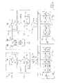
- FIG. 1An example of a prior art sense amplifier circuit is shown in FIG. 1 .
- This sense amplifier circuitis similar to a sense amplifier described in U.S. Pat. No. 6,469,929 to Alexander Kushnarenko and Oleg Dadashev, entitled “Structure and method for high speed sensing of memory array”.
- FIG. 1illustrates a prior art sensing system for a memory array 110 , which includes a plurality of memory cells arranged in any number of rows and columns.
- a memory cell 111is to be read (i.e. sensed).
- Memory cell 111has its drain and source terminals coupled to array bit lines BN and BN+1 and its control terminal coupled to a word line W 1 .
- Memory cell 111is selectively coupled to a system bit line BL using a column decoder 104 (for selecting the array bit lines) and a row decoder 103 (for selecting the word lines).
- the system bit line BLmay include an associated parasitic capacitance CBL that is proportional to the number of memory cells coupled to the selected array bit line.
- a memory cell 113has its drain and source terminals coupled to array bit lines BM and BM+1 and its control terminal coupled to a word line W 1 .
- Memory cell 113is selectively coupled to a system bit line BL_REF using a column decoder 105 (for selecting the array bit lines) and a tow decoder 106 (for selecting the word lines).
- the system bit line BLmay include an associated parasitic capacitance CREF_BL that is proportional to the number of memory cells coupled to the selected array bit line.
- the array bit line BNis coupled to the system bit line BL, the array bit line BN+1 is coupled to a predetermined voltage (e.g. ground), and the word line W 1 is coupled to a read voltage (e.g., 3 volts).
- a predetermined voltagee.g. ground
- the word line W 1is coupled to a read voltage (e.g., 3 volts).
- the system bit line BLmay be charged to a predetermined level (e.g., approximately 2V) before the sensing of memory cell 111 .
- the optimal charging of the system bit line BLmay facilitate a quick transition to the predetermined voltage without overshooting this predetermined voltage.
- This charging operationmay be initiated using a charge initiation device P 2 and advantageously controlled using a control unit 120 (control unit 121 for the right side of FIG. 1 ) that quickly and efficiently charges the system bit line BL.
- an active signal CHARGEturns on charge initiation device P 2 (P 7 for the right side of FIG. 1 ).
- Charge initiation device P 2may comprise a PMOS (p-channel metal oxide semiconductor) transistor, wherein the active signal CHARGE is a logic 0.
- charge initiation device P 2transfers a pull-up signal provided by the sense amplifier 145 (explained in detail below) to control unit 120 .
- Control unit 120may comprise a static clamp including an NMOS (n-channel metal oxide semiconductor) transistor N 1 (N 2 for the right side of FIG. 1 ) and a dynamic clamp including a PMOS transistor P 1 (P 8 for the right side of FIG. 1 ).
- the transistor N 1may have its drain connected to charge initiation device P 2 and its source connected to system bit line BL.
- Transistor N 1receives a bias voltage VB on its gate.
- Bias voltage VBis the gate bias voltage for transistor N 1 as defined by: VTN ⁇ VB ⁇ VBLD+VTN
- VLDis the desired voltage on bit line BL and VTN is the threshold voltage of the n-type transistor (e.g., 0.6V).
- VTNis the threshold voltage of the n-type transistor (e.g., 0.6V).
- transistor N 1charges bit line BL very quickly to VB-VTN.
- transistor N 1transitions to non-conducting, i.e. the static clamp deactivates, and the dynamic clamp is activated (as explained below).
- the dynamic clamp of control unit 120may include PMOS transistor P 1 having its source connected to charge initiation device P 2 (also the drain of transistor N 1 ) and its drain coupled to bit line BL (also the source of transistor N 1 ).
- the dynamic clampfurther comprises a comparator C 1 (C 2 for the right side of FIG. 1 ), which compares a reference voltage BIAS and the bit line voltage BL and then outputs a signal VG representative of that comparison. Specifically, comparator C 1 outputs a low signal VG if VBL is less than BIAS and outputs a high signal VG if VBL is greater than BIAS (or if comparator C 1 is disabled).
- the reference voltage BIASmay be approximately equal to the desired bit line voltage VBLD on the system bit line BL.
- the transistor P 1receives the signal VG on its control gate.
- Sense amplifier 145may include first stages 130 and 131 and second stage 140 .
- the first stage 130includes a pull-up device N 4 , which is an NMOS transistor having its drain and gate connected to a supply voltage VDD and its source connected to charge initiation device P 2 , and a current sensing device P 3 , which is a PMOS transistor having its drain and gate connected to charge initiation device P 2 and its source connected to the supply voltage VDD.
- current sensing device P 3advantageously functions as a diode, which is explained in further detail below.
- the first stage 131has an identical configuration to first stage 130 .
- first stage 131includes a pull-up device N 3 , which is an NMOS transistor having its drain and gate connected to a supply voltage VDD and its source connected to charge initiation device P 7 , and a current sensing device P 6 , which is a PMOS transistor having its drain and gate connected to charge initiation device P 7 and its source connected to the supply voltage VDD.
- both pull-up transistor N 4 (N 3 ) and current sensing device P 3 (P 6 )conduct strongly.
- the system bit line BLinitially receives a pull-up voltage of VDD-VTN via pull-up transistor N 4 (N 3 ).
- the voltage on the system bit line BLincreases to VDD-VTP, wherein VTP is the threshold voltage of the PMOS transistor Note that the voltage VDD-VTP is substantially equal to the desired system bit line voltage VBLD. At this point, this increased voltage on the system bit line BL turns off pull-up transistor N 4 (N 3 ).
- current sensing device P 3 (P 6 )is connected as a diode, only current IBL (IBL_REF) is detected. Therefore, depending on the state of the sensed memory cell, a predetermined current can flow through current sensing device P 3 (P 6 ).
- Current sensing devices P 3 and P 6 in first stages 130 and 131have current mirrors provided in second stage 140 . Specifically, the current IBL through current sensing device P 3 is reflected in the current I 1 through a PMOS transistor P 4 , whereas the current IBL_REF through current sensing device P 6 is reflected in the current I 2 through a PMOS transistor P 5 .
- the ratio of the currents through current sensing device P 3 and PMOS transistor P 4defines the gain of first stage 130 , whereas the ratio of the current through current sensing device P 6 and PMOS transistor P 6 defines the gain of first stage 131 .
- a latch circuit 141e.g., amplifier block
- VDD_MINV DIODE — MAX +V BL — MIN +V P1/P8 +V P2/P7 (1)
- VDIODE_MAXis the maximum voltage drop across PMOS transistor P 3 or PMOS transistor P 6
- VBL_MINis the minimum acceptable bit line voltage for the non-volatile memory technology
- VP 1 /P 8is the drain-to-source voltage drop of PMOS transistor P 1 (or PMOS transistor PS)
- VP 2 /P 7equal to the drain-to-source voltage drop on PMOS transistor P 2 (or PMOS transistor P 7 ).
- VDIODE_MAXis equal to 1.0 Volt
- VBL_MINis equal to 1.8 Volts
- VP 1 /P 8 and VP 2 /P 7are equal to 0.05 Volts
- the minimum supply voltage VDD_MINis equal to 2.9 Volts (1.8V+1V+0.05V+0.05V). In such a case, memory device 100 would not be usable in applications that use a VDD supply voltage lower than 2.9 Volts.
- sense amplifier first stages 130 and 131are sensitive to noise in the VDD supply voltage. If, during a read operation, the VDD supply voltage rises to an increased voltage of VDD_OVERSHOOT, then the voltages VSA 1 and VSA 2 on the drains of PMOS transistors P 3 and P 6 rise to a level approximately equal to VDD_OVERSHOOT minus a diode voltage drop. If the VDD supply voltage then falls to a reduced voltage of VDD_UNDERSHOOT, then transistors P 3 and P 6 may be turned off. At this time, sense amplifier first stages 130 and 131 cannot operate until the cell currents IBL and IBL_REF discharge the voltages VSA 1 and VSA 2 . If the cell current IBL is low, then sense amplifier first stage 130 will remain turned off until the end of the read operation, thereby causing the read operation to fail.
- the present inventionseeks to provide apparatus and methods for multi-level sensing in a memory arrays as is described more in detail hereinbelow.
- the present inventionenables multilevel sensing at a lower voltage operation.
- the multi-level sensingmay not be sensitive to Vdd noise (over/under shoots).
- a method for sensing a signal received from an array cell within a memory arrayincluding the steps of generating an analog voltage Vddr proportional to a current of a selected array cell of the memory array, and comparing the analog voltage Vddr with a reference analog voltage Vcomp to generate an output digital signal.
- the methodfurther includes providing a reference unit with a reference cell having a similar structure and a similar current path therethrough to that of the array cell, and providing a drain driver for driving drain bit lines of the memory array and reference drain bit lines of the reference unit, wherein the drain driver generates the analog voltage Vddr.
- analog voltage Vddris greater than the reference analog voltage Vcomp then a low output digital signal is output, and if the analog voltage Vddr is not greater than the reference analog voltage Vcomp then a high output digital signal is output.
- the methodfurther includes discharging the memory array and the reference unit, charging the memory array and the reference unit so as to generate an array cell signal and a reference signal, respectively, and a timing signal, generating a read signal when the timing signal reaches a predefined voltage level, and generating a sensing signal from the difference of the cell and reference signals once the read signal is generated.
- a method for sensing a memory cellincluding the steps of transforming a signal from a memory cell to a time delay, and sensing the memory cell by comparing the time delay to a time delay of a reference cell.
- the time delaymay include a digital signal delay. At least one of rise and fall times of the time delays may be compared.
- Transforming the signal from the memory cell to the time delaymay include generating an analog voltage Vddr proportional to a current of the memory cell.
- the analog voltage Vddrmay be compared with a reference analog voltage Vcomp to generate an output digital signal.
- apparatusfor sensing a signal received from an array cell within a memory array, the apparatus including a drain driver adapted to generate an analog voltage Vddr proportional to a current of a selected array cell of the memory array, and a comparator adapted to compare the analog voltage Vddr with a reference analog voltage Vcomp to generate an output digital signal.
- a reference unitmay be provided with a reference cell having a similar structure and a similar current path therethrough to that of the array cell, wherein the drain driver is adapted to drive drain bit lines of the memory array and reference drain bit lines of the reference unit.
- a data unitmay receive the output digital signal.
- the comparatorcompares the analog voltage Vddr with a reference analog voltage Vcomp and generates the output digital signal in the following manner: if the analog voltage Vddr is greater than the reference analog voltage Vcomp then a low output digital signal is output, and if the analog voltage Vddr is not greater than the reference analog voltage Vcomp then a high output digital signal is output.
- apparatus for sensing a memory cellincluding a driver adapted to transform a signal from a memory cell to a time delay, and a comparator adapted to compare the time delay to a time delay of a reference cell.
- FIG. 1is a simplified illustration of a prior art sensing system for a memory array, which includes a plurality of memory cells arranged in any number of rows and columns;
- FIG. 2is a simplified block diagram of a memory sensing system, constructed and operative in accordance with an embodiment of the present invention
- FIG. 3is a simplified block diagram of a memory cell array, which may be read by the memory sensing system, in accordance with an embodiment of the present invention
- FIG. 4is a simplified block diagram of a drain driver of the memory sensing system, constructed and operative in accordance with an embodiment of the present invention
- FIG. 5is a simplified graphical illustration of waveforms of the drain driver signals, in accordance with an embodiment of the present invention.
- FIG. 6is a simplified graphical illustration of waveforms of comparator signals of the memory sensing system of FIG. 2 , in accordance with an embodiment of the present invention
- FIG. 7is a simplified block diagram of a data unit of the memory sensing system, constructed and operative in accordance with an embodiment of the present invention.
- FIG. 8is a simplified graphical illustration of the distribution of the threshold voltages of reference memory cells of the memory sensing system, in accordance with an embodiment of the present invention.
- FIG. 9is a simplified graphical illustration of waveforms of the drain driver signals, in accordance with another embodiment of the present invention, different from that of FIG. 5 ;
- FIG. 10is a simplified block diagram of a memory sensing system, in accordance with another embodiment of the present invention.
- FIG. 11is a simplified block diagram of the drain driver for the embodiment of FIG. 10 , constructed and operative in accordance with an embodiment of the present invention.
- FIG. 12is a simplified graphical illustration of the waveforms of the drain driver signals, for the embodiment of FIG. 10 .
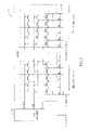
- FIG. 2illustrates a memory sensing system, constructed and operative in accordance with an embodiment of the present invention.
- FIG. 3illustrates a memory cell array 10 , which may be read by the memory sensing system, in accordance with an embodiment of the present invention.
- Memory cells of array 10are arranged in row and columns, and each memory cell is accessed during read, program, or erase operations by applying appropriate voltages associated word and bit lines.
- the gate terminal of memory cell MCjiis preferably connected to an associated word line (WL) WLi
- the drain and source terminalsare preferably connected to associated bit lines (BLs) BLj and BLj+1.
- Memory cells of array 10may be addressed using a word line control circuit, i.e., row decoder 12 , and a bit line control circuit, i.e., column decoder 14 , according to input addresses signals Xaddr ⁇ h: 0 > and Yaddr ⁇ p: 0 >, respectively.
- Row decoder 12provides an appropriated word line voltage to WL.
- Column decoder 14connects selected drain bit lines (DBL) and source bit lines (SBL) of a memory cell to DBL and SBL inputs correspondingly.
- DBLdrain bit lines
- SBLsource bit lines
- a plurality of memory cells connected to the same selected word linemay be accessed simultaneously.
- k+1 memory cellsmay be accessed simultaneously
- column decoder 14may have k+1 DBL and SBL nodes.
- the nodes SBL ⁇ k: 0 >may be connected to ground (GND) during the read operation.
- the source voltage of the selected memory cellsmay be close to GND.
- the memory sensing systemmay comprise one or more reference units 16 with one or more reference memory cells (RMCs) having a structure and current path therethrough similar to that of the array cells.
- the reference unitmay emulate the elements found in the current path from node DBL through MC to be read to node SBL. This may provide RC (resistance-capacitance) matching of the two paths.
- Drain drivers 18may be provided for driving the drain bit lines of array 10 and the reference drain bit lines of reference units 16 .
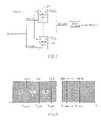
- FIG. 4illustrates an example of a suitable drain driver 18 , in accordance with an embodiment of the present invention.
- Drain driver 18may comprise a PMOS (p-channel metal oxide semiconductor) pull-up transistor M 0 , wherein its gate terminal receives a logical signal input (chargeb), its source terminal receives a voltage input Vps and its drain terminal is connected to a node 20 .
- PMOSp-channel metal oxide semiconductor
- An NMOS (n-channel metal oxide semiconductor) clamp transistor M 1may provided whose drain terminal is connected to the drain terminal of PMOS pull-up transistor M 0 via node 20 , whose gate terminal receives an input Vblr and whose source terminal is connected to the DBL input of the column decoder 14 .
- An integrated capacitor Cintmay be connected to a node 21 , which is connected to a node 20 and a node ddr.
- Drain driver 18may execute two functions during a read operation:
- the voltage Vpsenters the drain of the NMOS clamp transistor M 1 through the open PMOS pull-up transistor M 0 .
- the reduced voltageis transferred from the column decoder 14 to the drain terminal of the memory cell of the array 10 .
- FIG. 5illustrates waveforms of the drain driver signals, in accordance with an embodiment of the present invention.
- a logical signal chargebis high and therefore PMOS pull-up transistor M 0 is turned off (not conducting).
- the signal chargebgoes down to 0V and turns on PMOS pull-up transistor M 0 (i.e., it is now conducting).
- the signal ddrrises to Vps, and the drain bit line of the selected memory cell (both DBL nodes) becomes charged to voltage Vd. Current begins to flow through the memory cell. After the charging process to Vd is completed, the current of the path asymptotically stabilizes at the memory cell (MC) read current level, IMC.
- a signal boostmay be optionally coupled to ground.
- the signal boostmay rise from 0V to Vboost.
- C ⁇is the total capacity of the node ddr
- Cintis significantly greater than other (parasitic) capacitors of the node ddr, C ⁇ Cint and Vbst ⁇ Vboost.
- I ⁇is the current though node DBL ⁇ , which equals I MC .
- Vddris greater than Vd by some margin (e.g., on the order of about 0.2-0.3V) the NMOS transistor M 1 works in saturation.
- the capacitance of the node ddrmay be independent from the drain bit line capacitance, which may be a few orders of magnitude greater than Cint.
- the voltage of the nodes DBL, and BLmay remain at Vd during the time that Vddr(t) is developing, and therefore the drain-source voltage of the selected memory cell MCji remains constant as well.
- I ⁇is the read current of ⁇ -th reference memory cell.
- the memory sensing systemmay comprise one or more comparators 22 for array 10 (i.e., comparators ⁇ 0 :k>) and for reference units 16 (i.e., comparators ⁇ ref 0 :refm>).
- Comparator 22compares the analog voltage Vddr with a reference analog voltage Vcomp and generates an output digital signal amp according to the follow rule shown in Table 1:
- a voltage of the signal Vcompis disposed in an interval [Vd, Vps+Vbst].
- T 1 to T 2all signals cmp ⁇ 0 :k> are low (logical level “0”).
- the values Tcs ⁇ and Trcs ⁇are an inverse function of the memory cell current.
- FIG. 6illustrates waveforms of the comparator signals, in accordance with an embodiment of the present invention and the above explanation.
- each comparator signal of the comparators 22may be transmitted to the input of a data unit 24 together with the output signals lat ⁇ m: 0 > of the reference comparators.
- FIG. 7illustrates one example of data unit 24 , constructed and operative in accordance with an embodiment of the present invention.
- the signal cmpis provided to the D-input of m digital latches 26 , Each digital latch 26 may receive one of the tat signals of the reference comparators at its Eb-input.
- the digital latches 26may function according to the follow rule shown in Table 3:
- the digital latch 26When the Eb signal is a low level (logical “0”), the digital latch 26 transmits input signal D to output Q. When the Eb signal goes to a high level (logical “1”), the digital latch 26 transmits whatever the previous value was to output Q.
- the reference units 16may comprise reference memory cells (Ref 0 to Refm).
- Reference is now made to FIG. 8which illustrates a distribution of the threshold voltages (Vtref 0 to Vtrefm) of the reference memory cells, in accordance with an embodiment of the present invention.
- the threshold voltagesmay be distributed in m+1 zones in intervals along the Vt axis.
- the threshold voltage Vto of some cellwhich corresponds with the channel number ⁇ of the sensing (dbl ⁇ >-ddr ⁇ > -cmp ⁇ a>), may be in zone ⁇ .
- the threshold voltage Vtois greater than the threshold voltages in the previous zones (that is, Vtref 0 to Vtref( ⁇ 1)), and less than the threshold voltages in the next zones (that is, Vtref ⁇ to Vtrefm).
- the current Io of that cellis greater than the current in the next zones (Iref ⁇ to Irefm), and less than the current in the previous zones (Iref 0 to Iref( ⁇ 1)).
- the signal cmp ⁇ > corresponding to that cellrises earlier than signals lat ⁇ > ⁇ lat ⁇ m>, and later than signals lat ⁇ 0 > ⁇ lat ⁇ 1>.
- V M1dsis the drain/source voltage of the transistor M 1 in the drain driver
- V cdis the column decoder voltage drop
- V MCdsis the drain/source voltage of the memory cell.
- the minimum supply voltage VDD_MIN of the prior artis equal to 2.9 V, and the prior art memory device 100 cannot be used in applications that use a VDD supply voltage lower than 2.9 V.
- the minimum supply voltage Vps_minis less than the prior art VDD_MIN (see equation (1) above in the background of the invention) by VDIODE_MAX, and approaches the minimal voltage VBL_MIN.
- VDIODE_MAXmay be approximately equal to one volt, for example. This means that the present invention may be used in applications that use a VDD supply voltage lower than 2.9 V, down to 1.9 V, an improvement of over 34%.
- the present inventionmay transform a signal (e.g., current) from the memory cell to a time delay (e.g., a digital signal delay) and compare the time delay to a time delay of a reference cell (e.g., the rise or fall times of the signals).
- the drain driveroperates at a low (close to minimal) voltage to generate the analog signal Vddr.
- the signal Vddris preferably linearly dependent upon the memory cell current.
- the memory cell currentis preferably integrated on the local capacitor.
- the present inventionmay he used as a multi-level sensing system for a multiplicity of reference units.
- the inventionmay also be used for a single reference unit.
- signals from the memory cellsare coupled in a one-to-one correspondence to the sense amplifiers.
- the sense amplifiersThere is the same number of signals as there are sense amplifiers.
- the reference memory cellsare coupled in parallel to all of the sense amplifiers. This results in a significant mismatch between two sense amplifier input signals, because one of them (from the array) is connected to a single sense amplifier whereas the other (from the reference) is connected to all of the sense amplifiers. The mismatch may lead to errors in read data.
- all the analog signals from the array cells and the reference cellsare matched, as described hereinabove.
- FIG. 9illustrates waveforms of the drain driver signals, in accordance with another embodiment of the present invention, different from that of FIG. 5 .
- node Vpsis connected to the system voltage supply Vdd until a time Tps, when power dissipation is maximal for charging the read path parasitic capacitors.
- the current through node Vpsis significantly lower (e.g., practical equal to IMC), and node Vps is switched to a higher voltage supply than Vdd.
- This embodimentmay be useful to increase the possible range of boosting Vddr.
- FIG. 10illustrates a memory sensing system, in accordance with another embodiment of the present invention
- FIG. 11illustrates the drain driver for the embodiment of FIG. 10
- the nodes SBL ⁇ k: 0 >may be connected to the comparator inputs instead of the ddr ⁇ k: 0 > signals, as shown in FIG. 10 .
- the drain driver circuitis a simplified version of the drain driver circuit of FIG. 4 .
- FIG. 12illustrates the waveforms of the drain driver signals, in accordance with this embodiment of the invention.
- the development of the signals SBL ⁇ k: 0 >may be as described in U.S. Pat. No. 6,128,226 to Eitan and Dadashev, assigned to the common assignee of the present application.
Landscapes
- Engineering & Computer Science (AREA)
- Computer Hardware Design (AREA)
- Read Only Memory (AREA)
- Measurement Of Current Or Voltage (AREA)
Abstract
Description
VTN<VB<VBLD+VTN
VDD
Vbst=Vboost*CΣ/Cint (2)
Vddrα(t)=Vps+Vboost−Iα*t/Cint, α=0,k (3)
Vrddrβ(t)=Vps+Vboost−Iβ*t/Cint, β=0,m (4)
| TABLE 1 | |||
| Input voltages relation | cmp | ||
| Vddr > Vcomp | low | ||
| Vddr < Vcomp | high | ||
Tcsα=T2+(Vps+Vboost−Vcomp)*Cint/Iα, α=0,k (5)
Trcsβ=T2+(Vps+Vboost−Vcomp)*Cint/Iβ, α=0,m (6)
| TABLE 2 |
| Trise(cmp) > Trise(latξ) |
| ξ |
| 0 ÷ | 0 ÷ (m − 1) | 0 ÷ (m − 2) | 0 ÷ (m − 3) | 0 ÷ (m − 4) | 0 ÷ (m − 5) | 0 ÷ (m − 6) | 0 ÷ (m − 7) | ||
| dt | 000 | 001 | 010 | 011 | 100 | 101 | 110 | 111 |
| TABLE 3 | |||
| Eb | Q | ||
| 0 | |||
| 1 | Hold | ||
Q<(τ−1):0>=0,Q<m:τ>=1.
dtdecimal=Q<0>+Q<1>+Q<2>+ . . . +Q<m−1>+Q<m>.
dtdecimal=dq<0>*2^0+dq<1>*2^1+dq<2>*2^2+dq<3>*2{circumflex over (0)}3+ . . . +dq<y>*2{circumflex over (0)}y.
or in table form in Table 4:
| TABLE 4 | ||
| 0 | 1 | 11 | 111 | 1111 | 11111 | 111111 | 1111111 | ||
| 0 | 1 | 2 | 3 | 4 | 5 | 6 | 7 | |
| 0 | 1 | 10 | 11 | 100 | 101 | 110 | 111 | |
m=2{circumflex over (0)}y−1,
or in table form in Table 5:
| TABLE 5 | ||
| 1 | 3 | 7 | 15 | 31 | ||
| 1 | 2 | 3 | 4 | 5 | |||
Vps—min=VM1ds+Vcd+VMCds+Vcd, (7)
where
Claims (20)
Priority Applications (1)
| Application Number | Priority Date | Filing Date | Title |
|---|---|---|---|
| US11/464,253US7532529B2 (en) | 2004-03-29 | 2006-08-14 | Apparatus and methods for multi-level sensing in a memory array |
Applications Claiming Priority (2)
| Application Number | Priority Date | Filing Date | Title |
|---|---|---|---|
| US10/810,683US7142464B2 (en) | 2003-04-29 | 2004-03-29 | Apparatus and methods for multi-level sensing in a memory array |
| US11/464,253US7532529B2 (en) | 2004-03-29 | 2006-08-14 | Apparatus and methods for multi-level sensing in a memory array |
Related Parent Applications (1)
| Application Number | Title | Priority Date | Filing Date |
|---|---|---|---|
| US10/810,683ContinuationUS7142464B2 (en) | 2003-04-29 | 2004-03-29 | Apparatus and methods for multi-level sensing in a memory array |
Publications (2)
| Publication Number | Publication Date |
|---|---|
| US20060285402A1 US20060285402A1 (en) | 2006-12-21 |
| US7532529B2true US7532529B2 (en) | 2009-05-12 |
Family
ID=35056605
Family Applications (2)
| Application Number | Title | Priority Date | Filing Date |
|---|---|---|---|
| US10/810,683Expired - LifetimeUS7142464B2 (en) | 2003-04-29 | 2004-03-29 | Apparatus and methods for multi-level sensing in a memory array |
| US11/464,253Expired - Fee RelatedUS7532529B2 (en) | 2004-03-29 | 2006-08-14 | Apparatus and methods for multi-level sensing in a memory array |
Family Applications Before (1)
| Application Number | Title | Priority Date | Filing Date |
|---|---|---|---|
| US10/810,683Expired - LifetimeUS7142464B2 (en) | 2003-04-29 | 2004-03-29 | Apparatus and methods for multi-level sensing in a memory array |
Country Status (3)
| Country | Link |
|---|---|
| US (2) | US7142464B2 (en) |
| TW (1) | TWI379306B (en) |
| WO (1) | WO2005091714A2 (en) |
Cited By (24)
| Publication number | Priority date | Publication date | Assignee | Title |
|---|---|---|---|---|
| US7859321B2 (en)* | 2004-12-30 | 2010-12-28 | Nxp B.V. | Monitoring the temperature dependence of the external capacitors of a charge pump and improved charge pumps based thereon |
| US8717802B2 (en) | 2010-09-13 | 2014-05-06 | International Business Machines Corporation | Reconfigurable multi-level sensing scheme for semiconductor memories |
| US20140233339A1 (en)* | 2013-02-18 | 2014-08-21 | Spansion Llc. | Apparatus and method to reduce bit line disturbs |
| US9460760B2 (en)* | 2015-01-23 | 2016-10-04 | Globalfoundries Inc. | Data-dependent self-biased differential sense amplifier |
| US9583163B2 (en) | 2015-02-03 | 2017-02-28 | Micron Technology, Inc. | Loop structure for operations in memory |
| US9589602B2 (en) | 2014-09-03 | 2017-03-07 | Micron Technology, Inc. | Comparison operations in memory |
| US9659605B1 (en) | 2016-04-20 | 2017-05-23 | Micron Technology, Inc. | Apparatuses and methods for performing corner turn operations using sensing circuitry |
| US9697876B1 (en) | 2016-03-01 | 2017-07-04 | Micron Technology, Inc. | Vertical bit vector shift in memory |
| US9741399B2 (en) | 2015-03-11 | 2017-08-22 | Micron Technology, Inc. | Data shift by elements of a vector in memory |
| US9747961B2 (en) | 2014-09-03 | 2017-08-29 | Micron Technology, Inc. | Division operations in memory |
| US9830999B2 (en) | 2014-06-05 | 2017-11-28 | Micron Technology, Inc. | Comparison operations in memory |
| US9892767B2 (en) | 2016-02-12 | 2018-02-13 | Micron Technology, Inc. | Data gathering in memory |
| US9898253B2 (en) | 2015-03-11 | 2018-02-20 | Micron Technology, Inc. | Division operations on variable length elements in memory |
| US9898252B2 (en) | 2014-09-03 | 2018-02-20 | Micron Technology, Inc. | Multiplication operations in memory |
| US9904515B2 (en) | 2014-09-03 | 2018-02-27 | Micron Technology, Inc. | Multiplication operations in memory |
| US9910637B2 (en) | 2016-03-17 | 2018-03-06 | Micron Technology, Inc. | Signed division in memory |
| US10032493B2 (en) | 2015-01-07 | 2018-07-24 | Micron Technology, Inc. | Longest element length determination in memory |
| US10043570B1 (en) | 2017-04-17 | 2018-08-07 | Micron Technology, Inc. | Signed element compare in memory |
| US10042608B2 (en) | 2016-05-11 | 2018-08-07 | Micron Technology, Inc. | Signed division in memory |
| US10147467B2 (en) | 2017-04-17 | 2018-12-04 | Micron Technology, Inc. | Element value comparison in memory |
| US10146537B2 (en) | 2015-03-13 | 2018-12-04 | Micron Technology, Inc. | Vector population count determination in memory |
| US10153008B2 (en) | 2016-04-20 | 2018-12-11 | Micron Technology, Inc. | Apparatuses and methods for performing corner turn operations using sensing circuitry |
| US10607665B2 (en) | 2016-04-07 | 2020-03-31 | Micron Technology, Inc. | Span mask generation |
| US11029951B2 (en) | 2016-08-15 | 2021-06-08 | Micron Technology, Inc. | Smallest or largest value element determination |
Families Citing this family (9)
| Publication number | Priority date | Publication date | Assignee | Title |
|---|---|---|---|---|
| US7312641B2 (en)* | 2004-12-28 | 2007-12-25 | Spansion Llc | Sense amplifiers with high voltage swing |
| US7558149B2 (en)* | 2006-01-24 | 2009-07-07 | Macronix International Co., Ltd. | Method and apparatus to control sensing time for nonvolatile memory |
| CN101536106B (en)* | 2006-11-08 | 2014-09-17 | Nxp股份有限公司 | Read enhancement for memory |
| US7580297B2 (en)* | 2007-03-30 | 2009-08-25 | Infineon Technologies Ag | Readout of multi-level storage cells |
| US20090129166A1 (en)* | 2007-11-15 | 2009-05-21 | Eduardo Maayan | Method, circuit and system for sensing a cell in a non-volatile memory array |
| CN103366804B (en)* | 2012-03-30 | 2017-10-13 | 硅存储技术公司 | The Nonvolatile memory devices of sense amplifier are injected with electric current |
| US9911492B2 (en)* | 2014-01-17 | 2018-03-06 | International Business Machines Corporation | Writing multiple levels in a phase change memory using a write reference voltage that incrementally ramps over a write period |
| CN112242172A (en)* | 2019-07-19 | 2021-01-19 | 四川省豆萁科技股份有限公司 | A NOR flash memory and its reference current comparison circuit |
| US11342010B2 (en)* | 2019-10-01 | 2022-05-24 | Macronix International Co., Ltd. | Managing bit line voltage generating circuits in memory devices |
Citations (577)
| Publication number | Priority date | Publication date | Assignee | Title |
|---|---|---|---|---|
| GB1297899A (en) | 1970-10-02 | 1972-11-29 | ||
| US3881180A (en) | 1971-11-30 | 1975-04-29 | Texas Instruments Inc | Non-volatile memory cell |
| US3895360A (en) | 1974-01-29 | 1975-07-15 | Westinghouse Electric Corp | Block oriented random access memory |
| US3952325A (en) | 1971-07-28 | 1976-04-20 | U.S. Philips Corporation | Semiconductor memory elements |
| US4016588A (en) | 1974-12-27 | 1977-04-05 | Nippon Electric Company, Ltd. | Non-volatile semiconductor memory device |
| US4017888A (en) | 1975-12-31 | 1977-04-12 | International Business Machines Corporation | Non-volatile metal nitride oxide semiconductor device |
| US4145703A (en) | 1977-04-15 | 1979-03-20 | Supertex, Inc. | High power MOS device and fabrication method therefor |
| JPS5453929U (en) | 1977-09-21 | 1979-04-14 | ||
| US4151021A (en) | 1977-01-26 | 1979-04-24 | Texas Instruments Incorporated | Method of making a high density floating gate electrically programmable ROM |
| US4173766A (en) | 1977-09-16 | 1979-11-06 | Fairchild Camera And Instrument Corporation | Insulated gate field-effect transistor read-only memory cell |
| US4173791A (en) | 1977-09-16 | 1979-11-06 | Fairchild Camera And Instrument Corporation | Insulated gate field-effect transistor read-only memory array |
| US4247861A (en) | 1979-03-09 | 1981-01-27 | Rca Corporation | High performance electrically alterable read-only memory (EAROM) |
| WO1981000790A1 (en) | 1979-09-13 | 1981-03-19 | Ncr Co | Silicon gate non-volatile memory device |
| US4257832A (en) | 1978-07-24 | 1981-03-24 | Siemens Aktiengesellschaft | Process for producing an integrated multi-layer insulator memory cell |
| US4281397A (en) | 1979-10-29 | 1981-07-28 | Texas Instruments Incorporated | Virtual ground MOS EPROM or ROM matrix |
| US4306353A (en) | 1979-06-13 | 1981-12-22 | Siemens Aktiengesellschaft | Process for production of integrated MOS circuits with and without MNOS memory transistors in silicon-gate technology |
| US4342102A (en) | 1980-06-18 | 1982-07-27 | Signetics Corporation | Semiconductor memory array |
| US4342149A (en) | 1979-11-23 | 1982-08-03 | Siemens Aktiengesellschaft | Method of making very short channel length MNOS and MOS devices by double implantation of one conductivity type subsequent to other type implantation |
| US4360900A (en) | 1978-11-27 | 1982-11-23 | Texas Instruments Incorporated | Non-volatile semiconductor memory elements |
| US4373248A (en) | 1978-07-12 | 1983-02-15 | Texas Instruments Incorporated | Method of making high density semiconductor device such as floating gate electrically programmable ROM or the like |
| US4380057A (en) | 1980-10-27 | 1983-04-12 | International Business Machines Corporation | Electrically alterable double dense memory |
| US4388705A (en) | 1981-10-01 | 1983-06-14 | Mostek Corporation | Semiconductor memory circuit |
| US4389705A (en) | 1981-08-21 | 1983-06-21 | Mostek Corporation | Semiconductor memory circuit with depletion data transfer transistor |
| US4404747A (en) | 1981-07-29 | 1983-09-20 | Schur, Inc. | Knife and sheath assembly |
| US4435786A (en) | 1981-11-23 | 1984-03-06 | Fairchild Camera And Instrument Corporation | Self-refreshing memory cell |
| US4448400A (en) | 1981-07-13 | 1984-05-15 | Eliyahou Harari | Highly scalable dynamic RAM cell with self-signal amplification |
| US4471373A (en) | 1980-02-27 | 1984-09-11 | Hitachi, Ltd. | Semiconductor integrated circuit device with memory MISFETS and thin and thick gate insulator MISFETS |
| US4494016A (en) | 1982-07-26 | 1985-01-15 | Sperry Corporation | High performance MESFET transistor for VLSI implementation |
| US4507673A (en) | 1979-10-13 | 1985-03-26 | Tokyo Shibaura Denki Kabushiki Kaisha | Semiconductor memory device |
| US4521796A (en) | 1980-12-11 | 1985-06-04 | General Instrument Corporation | Memory implant profile for improved channel shielding in electrically alterable read only memory semiconductor device |
| US4527257A (en) | 1982-08-25 | 1985-07-02 | Westinghouse Electric Corp. | Common memory gate non-volatile transistor memory |
| JPS60200566A (en) | 1984-03-26 | 1985-10-11 | Hitachi Ltd | Semiconductor integrated circuit device |
| JPS60201594A (en) | 1984-03-23 | 1985-10-12 | Hitachi Micro Comput Eng Ltd | semiconductor storage device |
| GB2157489A (en) | 1984-03-23 | 1985-10-23 | Hitachi Ltd | A semiconductor integrated circuit memory device |
| US4586163A (en) | 1982-09-13 | 1986-04-29 | Toshiba Shibaura Denki Kabushiki Kaisha | Multi-bit-per-cell read only memory circuit |
| US4613956A (en) | 1983-02-23 | 1986-09-23 | Texas Instruments Incorporated | Floating gate memory with improved dielectric |
| US4630085A (en) | 1984-02-28 | 1986-12-16 | Nec Corporation | Erasable, programmable read-only memory device |
| US4663645A (en) | 1984-05-23 | 1987-05-05 | Hitachi, Ltd. | Semiconductor device of an LDD structure having a floating gate |
| US4665426A (en) | 1985-02-01 | 1987-05-12 | Advanced Micro Devices, Inc. | EPROM with ultraviolet radiation transparent silicon nitride passivation layer |
| US4667217A (en) | 1985-04-19 | 1987-05-19 | Ncr Corporation | Two bit vertically/horizontally integrated memory cell |
| US4672409A (en) | 1980-12-25 | 1987-06-09 | Fujitsu Limited | Nonvolatile semiconductor memory device |
| US4725984A (en) | 1984-02-21 | 1988-02-16 | Seeq Technology, Inc. | CMOS eprom sense amplifier |
| US4733105A (en) | 1985-09-04 | 1988-03-22 | Oki Electric Industry Co., Ltd. | CMOS output circuit |
| US4742491A (en) | 1985-09-26 | 1988-05-03 | Advanced Micro Devices, Inc. | Memory cell having hot-hole injection erase mode |
| US4758869A (en) | 1986-08-29 | 1988-07-19 | Waferscale Integration, Inc. | Nonvolatile floating gate transistor structure |
| US4760555A (en) | 1986-04-21 | 1988-07-26 | Texas Instruments Incorporated | Memory array with an array reorganizer |
| US4761764A (en) | 1985-04-18 | 1988-08-02 | Nec Corporation | Programmable read only memory operable with reduced programming power consumption |
| US4769340A (en) | 1983-11-28 | 1988-09-06 | Exel Microelectronics, Inc. | Method for making electrically programmable memory device by doping the floating gate by implant |
| JPS63249375A (en) | 1987-04-06 | 1988-10-17 | Oki Electric Ind Co Ltd | Data erasing method for semiconductor memory device |
| US4780424A (en) | 1987-09-28 | 1988-10-25 | Intel Corporation | Process for fabricating electrically alterable floating gate memory devices |
| US4839705A (en) | 1987-12-16 | 1989-06-13 | Texas Instruments Incorporated | X-cell EEPROM array |
| US4847808A (en) | 1986-04-22 | 1989-07-11 | Nec Corporation | Read only semiconductor memory having multiple bit cells |
| US4857770A (en) | 1988-02-29 | 1989-08-15 | Advanced Micro Devices, Inc. | Output buffer arrangement for reducing chip noise without speed penalty |
| US4870470A (en) | 1987-10-16 | 1989-09-26 | International Business Machines Corporation | Non-volatile memory cell having Si rich silicon nitride charge trapping layer |
| US4888735A (en) | 1987-12-30 | 1989-12-19 | Elite Semiconductor & Systems Int'l., Inc. | ROM cell and array configuration |
| US4916671A (en) | 1988-09-06 | 1990-04-10 | Mitsubishi Denki Kabushiki Kaisha | Semiconductor memory device having sense amplifier having improved activation timing thereof and operating method thereof |
| US4941028A (en) | 1988-08-10 | 1990-07-10 | Actel Corporation | Structure for protecting thin dielectrics during processing |
| US4961010A (en) | 1989-05-19 | 1990-10-02 | National Semiconductor Corporation | Output buffer for reducing switching induced noise |
| US4992391A (en) | 1989-11-29 | 1991-02-12 | Advanced Micro Devices, Inc. | Process for fabricating a control gate for a floating gate FET |
| US5021999A (en) | 1987-12-17 | 1991-06-04 | Mitsubishi Denki Kabushiki Kaisha | Non-volatile semiconductor memory device with facility of storing tri-level data |
| US5027321A (en) | 1989-11-21 | 1991-06-25 | Intel Corporation | Apparatus and method for improved reading/programming of virtual ground EPROM arrays |
| US5029063A (en) | 1989-03-25 | 1991-07-02 | Eurosil Electronic Gmbh | MOSFET multiplying circuit |
| US5042009A (en) | 1988-12-09 | 1991-08-20 | Waferscale Integration, Inc. | Method for programming a floating gate memory device |
| JPH03285358A (en) | 1990-04-02 | 1991-12-16 | Matsushita Electron Corp | Driving method for nonvolatile semiconductor storage device |
| US5075245A (en) | 1990-08-03 | 1991-12-24 | Intel Corporation | Method for improving erase characteristics of buried bit line flash EPROM devices without using sacrificial oxide growth and removal steps |
| US5081371A (en) | 1990-11-07 | 1992-01-14 | U.S. Philips Corp. | Integrated charge pump circuit with back bias voltage reduction |
| US5086325A (en) | 1990-11-21 | 1992-02-04 | Atmel Corporation | Narrow width EEPROM with single diffusion electrode formation |
| US5094968A (en) | 1990-11-21 | 1992-03-10 | Atmel Corporation | Fabricating a narrow width EEPROM with single diffusion electrode formation |
| US5104819A (en) | 1989-08-07 | 1992-04-14 | Intel Corporation | Fabrication of interpoly dielctric for EPROM-related technologies |
| US5117389A (en) | 1990-09-05 | 1992-05-26 | Macronix International Co., Ltd. | Flat-cell read-only-memory integrated circuit |
| US5120672A (en) | 1989-02-22 | 1992-06-09 | Texas Instruments Incorporated | Fabricating a single level merged EEPROM cell having an ONO memory stack substantially spaced from the source region |
| JPH04226071A (en) | 1990-05-16 | 1992-08-14 | Ricoh Co Ltd | Semiconductor memory device |
| US5142495A (en) | 1989-03-10 | 1992-08-25 | Intel Corporation | Variable load for margin mode |
| US5142496A (en) | 1991-06-03 | 1992-08-25 | Advanced Micro Devices, Inc. | Method for measuring VT 's less than zero without applying negative voltages |
| JPH04291962A (en) | 1991-03-20 | 1992-10-16 | Fujitsu Ltd | Mask ROM manufacturing method and mask ROM |
| US5159570A (en) | 1987-12-22 | 1992-10-27 | Texas Instruments Incorporated | Four memory state EEPROM |
| US5168334A (en) | 1987-07-31 | 1992-12-01 | Texas Instruments, Incorporated | Non-volatile semiconductor memory |
| US5172338A (en) | 1989-04-13 | 1992-12-15 | Sundisk Corporation | Multi-state EEprom read and write circuits and techniques |
| US5175120A (en) | 1991-10-11 | 1992-12-29 | Micron Technology, Inc. | Method of processing a semiconductor wafer to form an array of nonvolatile memory devices employing floating gate transistors and peripheral area having CMOS transistors |
| US5204835A (en) | 1990-06-13 | 1993-04-20 | Waferscale Integration Inc. | Eprom virtual ground array |
| US5214303A (en) | 1991-02-08 | 1993-05-25 | Sharp Kabushiki Kaisha | Semiconductor device ROM having an offset region |
| JPH0521758Y2 (en) | 1986-05-19 | 1993-06-03 | ||
| US5237213A (en) | 1991-04-15 | 1993-08-17 | Oki Electric Industry Co., Ltd. | Semiconductor integrated circuit with low-noise output buffers |
| US5241497A (en) | 1990-06-14 | 1993-08-31 | Creative Integrated Systems, Inc. | VLSI memory with increased memory access speed, increased memory cell density and decreased parasitic capacitance |
| US5260593A (en) | 1991-12-10 | 1993-11-09 | Micron Technology, Inc. | Semiconductor floating gate device having improved channel-floating gate interaction |
| US5268861A (en) | 1991-04-10 | 1993-12-07 | Sharp Kabushiki Kaisha | Semiconductor read only memory |
| JPH05326893A (en) | 1992-05-25 | 1993-12-10 | Rohm Co Ltd | Non-volatile storage device |
| US5276646A (en) | 1990-09-25 | 1994-01-04 | Samsung Electronics Co., Ltd. | High voltage generating circuit for a semiconductor memory circuit |
| US5280420A (en) | 1992-10-02 | 1994-01-18 | National Semiconductor Corporation | Charge pump which operates on a low voltage power supply |
| US5289412A (en) | 1992-06-19 | 1994-02-22 | Intel Corporation | High-speed bias-stabilized current-mirror referencing circuit for non-volatile memories |
| US5293563A (en) | 1988-12-29 | 1994-03-08 | Sharp Kabushiki Kaisha | Multi-level memory cell with increased read-out margin |
| US5295108A (en) | 1992-04-08 | 1994-03-15 | Nec Corporation | Electrically erasable and programmable read only memory device with simple controller for selecting operational sequences after confirmation |
| US5295092A (en) | 1992-01-21 | 1994-03-15 | Sharp Kabushiki Kaisha | Semiconductor read only memory |
| US5305262A (en) | 1991-09-11 | 1994-04-19 | Kawasaki Steel Corporation | Semiconductor integrated circuit |
| US5311049A (en) | 1991-10-17 | 1994-05-10 | Rohm Co., Ltd. | Non-volatile semiconductor memory with outer drain diffusion layer |
| US5315541A (en) | 1992-07-24 | 1994-05-24 | Sundisk Corporation | Segmented column memory array |
| JPH06151833A (en) | 1992-11-16 | 1994-05-31 | Mitsubishi Electric Corp | Semiconductor device and manufacturing method thereof |
| US5324675A (en) | 1992-03-31 | 1994-06-28 | Kawasaki Steel Corporation | Method of producing semiconductor devices of a MONOS type |
| US5334555A (en) | 1991-11-06 | 1994-08-02 | Sony Corporation | Method of determining conditions for plasma silicon nitride film growth and method of manufacturing semiconductor device |
| US5335198A (en) | 1993-05-06 | 1994-08-02 | Advanced Micro Devices, Inc. | Flash EEPROM array with high endurance |
| US5338954A (en) | 1991-10-31 | 1994-08-16 | Rohm Co., Ltd. | Semiconductor memory device having an insulating film and a trap film joined in a channel region |
| JPH06232416A (en) | 1993-02-03 | 1994-08-19 | Rohm Co Ltd | Semiconductor storage device and manufacture thereof |
| US5345425A (en) | 1990-11-20 | 1994-09-06 | Fujitsu Limited | Semiconductor memory device |
| US5349221A (en) | 1991-10-25 | 1994-09-20 | Rohm Co., Ltd. | Semiconductor memory device and method of reading out information for the same |
| US5350710A (en) | 1993-06-24 | 1994-09-27 | United Microelectronics Corporation | Device for preventing antenna effect on circuit |
| US5352620A (en) | 1984-05-23 | 1994-10-04 | Hitachi, Ltd. | Method of making semiconductor device with memory cells and peripheral transistors |
| US5357134A (en) | 1991-10-31 | 1994-10-18 | Rohm Co., Ltd. | Nonvolatile semiconductor device having charge trap film containing silicon crystal grains |
| US5359554A (en) | 1991-08-27 | 1994-10-25 | Matsushita Electric Industrial Co., Ltd. | Semiconductor memory device having an energy gap for high speed operation |
| US5361343A (en) | 1991-07-30 | 1994-11-01 | Intel Corporation | Microprocessor system including first and second nonvolatile memory arrays which may be simultaneously read and reprogrammed |
| US5366915A (en) | 1992-08-28 | 1994-11-22 | Nec Corporation | Process of fabricating floating gate type field effect transistor having drain region gently varied in impurity profile |
| US5375094A (en) | 1992-06-19 | 1994-12-20 | Kabushiki Kaisha Toshiba | Nonvolatile semiconductor memory system with a plurality of erase blocks |
| US5381374A (en) | 1992-01-09 | 1995-01-10 | Kabushiki Kaisha Toshiba | Memory cell data output circuit having improved access time |
| US5394355A (en) | 1990-08-28 | 1995-02-28 | Mitsubishi Denki Kabushiki Kaisha | Read only memory for storing multi-data |
| US5393701A (en) | 1993-04-08 | 1995-02-28 | United Microelectronics Corporation | Layout design to eliminate process antenna effect |
| US5399891A (en) | 1992-01-22 | 1995-03-21 | Macronix International Co., Ltd. | Floating gate or flash EPROM transistor array having contactless source and drain diffusions |
| US5400286A (en) | 1993-08-17 | 1995-03-21 | Catalyst Semiconductor Corp. | Self-recovering erase scheme to enhance flash memory endurance |
| US5402374A (en) | 1993-04-30 | 1995-03-28 | Rohm Co., Ltd. | Non-volatile semiconductor memory device and memory circuit using the same |
| US5412601A (en) | 1992-08-31 | 1995-05-02 | Nippon Steel Corporation | Non-volatile semiconductor memory device capable of storing multi-value data in each memory cell |
| US5414693A (en) | 1991-08-29 | 1995-05-09 | Hyundai Electronics Industries Co., Ltd. | Self-aligned dual-bit split gate (DSG) flash EEPROM cell |
| US5418176A (en) | 1994-02-17 | 1995-05-23 | United Microelectronics Corporation | Process for producing memory devices having narrow buried N+ lines |
| US5418743A (en) | 1992-12-07 | 1995-05-23 | Nippon Steel Corporation | Method of writing into non-volatile semiconductor memory |
| US5422844A (en) | 1992-12-21 | 1995-06-06 | National Semiconductor Corporation | Memory array with field oxide islands eliminated and method |
| US5424567A (en) | 1991-05-15 | 1995-06-13 | North American Philips Corporation | Protected programmable transistor with reduced parasitic capacitances and method of fabrication |
| US5424978A (en) | 1993-03-15 | 1995-06-13 | Nippon Steel Corporation | Non-volatile semiconductor memory cell capable of storing more than two different data and method of using the same |
| US5426605A (en) | 1992-08-19 | 1995-06-20 | U.S. Philips Corporation | Semiconductor memory device |
| US5434825A (en) | 1988-06-08 | 1995-07-18 | Harari; Eliyahou | Flash EEPROM system cell array with more than two storage states per memory cell |
| US5436478A (en) | 1994-03-16 | 1995-07-25 | National Semiconductor Corporation | Fast access AMG EPROM with segment select transistors which have an increased width |
| US5436481A (en) | 1993-01-21 | 1995-07-25 | Nippon Steel Corporation | MOS-type semiconductor device and method of making the same |
| JPH07193151A (en) | 1993-12-27 | 1995-07-28 | Toshiba Corp | Nonvolatile semiconductor memory device and its storage method |
| US5440505A (en) | 1994-01-21 | 1995-08-08 | Intel Corporation | Method and circuitry for storing discrete amounts of charge in a single memory element |
| US5450354A (en) | 1992-08-31 | 1995-09-12 | Nippon Steel Corporation | Non-volatile semiconductor memory device detachable deterioration of memory cells |
| US5450341A (en) | 1992-08-31 | 1995-09-12 | Nippon Steel Corporation | Non-volatile semiconductor memory device having memory cells, each for at least three different data writable thereinto selectively and a method of using the same |
| US5455793A (en) | 1992-01-15 | 1995-10-03 | National Semiconductor Corp. | Electrically reprogrammable EPROM cell with merged transistor and optimum area |
| US5467308A (en) | 1994-04-05 | 1995-11-14 | Motorola Inc. | Cross-point eeprom memory array |
| US5477499A (en) | 1993-10-13 | 1995-12-19 | Advanced Micro Devices, Inc. | Memory architecture for a three volt flash EEPROM |
| US5495440A (en) | 1993-01-19 | 1996-02-27 | Mitsubishi Denki Kabushiki Kaisha | Semiconductor memory device having hierarchical bit line structure |
| US5496753A (en) | 1992-05-29 | 1996-03-05 | Citizen Watch, Co., Ltd. | Method of fabricating a semiconductor nonvolatile storage device |
| US5508968A (en) | 1994-08-12 | 1996-04-16 | International Business Machines Corporation | Dynamic random access memory persistent page implemented as processor register sets |
| JPH08106791A (en) | 1994-10-03 | 1996-04-23 | Matsushita Electric Ind Co Ltd | Driving method for semiconductor memory device |
| US5518942A (en) | 1995-02-22 | 1996-05-21 | Alliance Semiconductor Corporation | Method of making flash EPROM cell having improved erase characteristics by using a tilt angle implant |
| WO1996015553A1 (en) | 1994-11-15 | 1996-05-23 | Advanced Micro Devices, Inc. | Transistor structure with specific gate and pad areas |
| US5521870A (en) | 1993-12-07 | 1996-05-28 | Nec Corporation | Semiconductor memory device having a coincidence detection circuit and its test method |
| US5523251A (en) | 1994-10-05 | 1996-06-04 | United Microelectronics Corp. | Method for fabricating a self aligned mask ROM |
| US5523972A (en) | 1994-06-02 | 1996-06-04 | Intel Corporation | Method and apparatus for verifying the programming of multi-level flash EEPROM memory |
| US5530803A (en) | 1994-04-14 | 1996-06-25 | Advanced Micro Devices, Inc. | Method and apparatus for programming memory devices |
| US5534804A (en) | 1995-02-13 | 1996-07-09 | Advanced Micro Devices, Inc. | CMOS power-on reset circuit using hysteresis |
| US5537358A (en) | 1994-12-06 | 1996-07-16 | National Semiconductor Corporation | Flash memory having adaptive sensing and method |
| US5544116A (en) | 1993-08-31 | 1996-08-06 | Macronix International Co., Ltd. | Erase and program verification circuit for non-volatile memory |
| US5553030A (en) | 1993-09-10 | 1996-09-03 | Intel Corporation | Method and apparatus for controlling the output voltage provided by a charge pump circuit |
| US5553018A (en) | 1995-06-07 | 1996-09-03 | Advanced Micro Devices, Inc. | Nonvolatile memory cell formed using self aligned source implant |
| US5557570A (en) | 1992-05-28 | 1996-09-17 | Kabushiki Kaisha Toshiba | Nonvolatile semiconductor memory device |
| US5557221A (en) | 1992-06-15 | 1996-09-17 | Fujitsu Limited | Semiconductor integrated circuit with input/output interface adapted for small-amplitude operation |
| US5559687A (en) | 1993-06-21 | 1996-09-24 | Sgs-Thomson Microelectronics, S.R.L. | Voltage multiplier for high output current with stabilized output voltage |
| US5563823A (en) | 1993-08-31 | 1996-10-08 | Macronix International Co., Ltd. | Fast FLASH EPROM programming and pre-programming circuit design |
| US5568085A (en) | 1994-05-16 | 1996-10-22 | Waferscale Integration Inc. | Unit for stabilizing voltage on a capacitive node |
| JPH08297988A (en) | 1995-04-27 | 1996-11-12 | Sony Corp | Semiconductor nonvolatile memory |
| US5579199A (en) | 1992-11-26 | 1996-11-26 | Sharp Kabushiki Kaisha | Non-volatile memory device and a method for producing the same |
| US5581252A (en) | 1994-10-13 | 1996-12-03 | Linear Technology Corporation | Analog-to-digital conversion using comparator coupled capacitor digital-to-analog converters |
| US5583808A (en) | 1994-09-16 | 1996-12-10 | National Semiconductor Corporation | EPROM array segmented for high performance and method for controlling same |
| US5590068A (en) | 1993-02-01 | 1996-12-31 | National Semiconductor Corporation | Ultra-high density alternate metal virtual ground ROM |
| US5590074A (en) | 1991-12-27 | 1996-12-31 | Fujitsu Limited | Nonvolatile semiconductor memory |
| US5592417A (en) | 1994-01-31 | 1997-01-07 | Sgs-Thomson Microelectronics S.A. | Non-volatile programmable bistable multivibrator, programmable by the source, for memory redundancy circuit |
| JPH0917981A (en) | 1995-07-03 | 1997-01-17 | Hitachi Ltd | Semiconductor memory device |
| US5599727A (en) | 1994-12-15 | 1997-02-04 | Sharp Kabushiki Kaisha | Method for producing a floating gate memory device including implanting ions through an oxidized portion of the silicon film from which the floating gate is formed |
| US5600586A (en) | 1994-05-26 | 1997-02-04 | Aplus Integrated Circuits, Inc. | Flat-cell ROM and decoder |
| WO1996025741A3 (en) | 1995-02-16 | 1997-02-06 | Siemens Ag | Multi-valued read-only storage location with improved signal-to-noise ratio |
| US5604804A (en) | 1996-04-23 | 1997-02-18 | Micali; Silvio | Method for certifying public keys in a digital signature scheme |
| US5606523A (en) | 1994-01-31 | 1997-02-25 | Sgs-Thomson Microelectronics S.A. | Non-volatile programmable bistable multivibrator in predefined initial state for memory redundancy circuit |
| US5608679A (en) | 1994-06-02 | 1997-03-04 | Intel Corporation | Fast internal reference cell trimming for flash EEPROM memory |
| US5612642A (en) | 1995-04-28 | 1997-03-18 | Altera Corporation | Power-on reset circuit with hysteresis |
| US5617357A (en) | 1995-04-07 | 1997-04-01 | Advanced Micro Devices, Inc. | Flash EEPROM memory with improved discharge speed using substrate bias and method therefor |
| US5623438A (en) | 1992-11-30 | 1997-04-22 | Sgs-Thomson Microelectronics, Inc. | Virtual ground read only memory circuit |
| US5627790A (en) | 1994-03-22 | 1997-05-06 | Sgs-Thomson Microelectronics S.R.L. | Reading circuit for an integrated semiconductor memory device |
| US5633603A (en) | 1995-12-26 | 1997-05-27 | Hyundai Electronics Industries Co., Ltd. | Data output buffer using pass transistors biased with a reference voltage and a precharged data input |
| US5636288A (en) | 1995-02-16 | 1997-06-03 | Paradigm Electronics Inc. | Standby power circuit arrangement |
| JPH09162314A (en) | 1995-12-12 | 1997-06-20 | Nec Corp | Nonvolatile semiconductor storage device and storage method |
| US5644531A (en) | 1995-11-01 | 1997-07-01 | Advanced Micro Devices, Inc. | Program algorithm for low voltage single power supply flash memories |
| US5654568A (en) | 1992-01-17 | 1997-08-05 | Rohm Co., Ltd. | Semiconductor device including nonvolatile memories |
| US5657332A (en) | 1992-05-20 | 1997-08-12 | Sandisk Corporation | Soft errors handling in EEPROM devices |
| US5661060A (en) | 1994-12-28 | 1997-08-26 | National Semiconductor Corporation | Method for forming field oxide regions |
| US5663907A (en) | 1996-04-25 | 1997-09-02 | Bright Microelectronics, Inc. | Switch driver circuit for providing small sector sizes for negative gate erase flash EEPROMS using a standard twin-well CMOS process |
| US5666365A (en) | 1995-03-16 | 1997-09-09 | Bell Atlantic Network Services, Inc. | Simulcast transmission of digital programs to shared antenna receiving systems |
| US5672959A (en) | 1996-04-12 | 1997-09-30 | Micro Linear Corporation | Low drop-out voltage regulator having high ripple rejection and low power consumption |
| US5675280A (en) | 1993-06-17 | 1997-10-07 | Fujitsu Limited | Semiconductor integrated circuit device having built-in step-down circuit for stepping down external power supply voltage |
| US5677867A (en) | 1991-06-12 | 1997-10-14 | Hazani; Emanuel | Memory with isolatable expandable bit lines |
| US5677869A (en) | 1995-12-14 | 1997-10-14 | Intel Corporation | Programming flash memory using strict ordering of states |
| US5683925A (en) | 1996-06-13 | 1997-11-04 | Waferscale Integration Inc. | Manufacturing method for ROM array with minimal band-to-band tunneling |
| US5689459A (en) | 1994-03-03 | 1997-11-18 | Rohm Corporation | Low voltage one transistor flash EEPROM cell using Fowler-Nordheim programming and erase |
| US5694356A (en) | 1994-11-02 | 1997-12-02 | Invoice Technology, Inc. | High resolution analog storage EPROM and flash EPROM |
| US5696929A (en) | 1995-10-03 | 1997-12-09 | Intel Corporation | Flash EEPROM main memory in a computer system |
| US5708608A (en) | 1995-12-28 | 1998-01-13 | Hyundai Electronics Industries Cp., Ltd. | High-speed and low-noise output buffer |
| US5712815A (en) | 1996-04-22 | 1998-01-27 | Advanced Micro Devices, Inc. | Multiple bits per-cell flash EEPROM capable of concurrently programming and verifying memory cells and reference cells |
| US5712814A (en) | 1994-07-18 | 1998-01-27 | Sgs-Thomson Microelectronics S.R.L. | Nonvolatile memory cell and a method for forming the same |
| WO1998003977A1 (en) | 1996-07-23 | 1998-01-29 | Saifun Semiconductors Ltd. | Non-volatile semiconductor memory cell utilizing asymmetrical charge trapping |
| US5715193A (en) | 1996-05-23 | 1998-02-03 | Micron Quantum Devices, Inc. | Flash memory system and method for monitoring the disturb effect on memory cell blocks due to high voltage conditions of other memory cell blocks |
| US5717635A (en) | 1996-08-27 | 1998-02-10 | International Business Machines Corporation | High density EEPROM for solid state file |
| US5717581A (en) | 1994-06-30 | 1998-02-10 | Sgs-Thomson Microelectronics, Inc. | Charge pump circuit with feedback control |
| US5717632A (en) | 1996-11-27 | 1998-02-10 | Advanced Micro Devices, Inc. | Apparatus and method for multiple-level storage in non-volatile memories |
| US5721781A (en) | 1995-09-13 | 1998-02-24 | Microsoft Corporation | Authentication system and method for smart card transactions |
| US5726946A (en) | 1994-06-02 | 1998-03-10 | Mitsubishi Denki Kabushiki Kaisha | Semiconductor integrated circuit device having hierarchical power source arrangement |
| JPH10106276A (en) | 1996-09-30 | 1998-04-24 | Hitachi Ltd | Semiconductor integrated circuit and data processing system |
| US5748534A (en) | 1996-03-26 | 1998-05-05 | Invox Technology | Feedback loop for reading threshold voltage |
| US5751037A (en) | 1995-07-27 | 1998-05-12 | Sony Corporation | Non-volatile memory cell having dual gate electrodes |
| US5751637A (en) | 1995-06-07 | 1998-05-12 | Macronix International Co., Ltd. | Automatic programming algorithm for page mode flash memory with variable programming pulse height and pulse width |
| US5754475A (en) | 1996-06-24 | 1998-05-19 | Advanced Micro Devices, Inc. | Bit line discharge method for reading a multiple bits-per-cell flash EEPROM |
| EP0843398A2 (en) | 1996-11-18 | 1998-05-20 | WaferScale Integration Inc. | Backup battery switch |
| US5760634A (en) | 1996-09-12 | 1998-06-02 | United Microelectronics Corporation | High speed, low noise output buffer |
| US5760445A (en) | 1994-09-13 | 1998-06-02 | Hewlett-Packard Company | Device and method of manufacture for protection against plasma charging damage in advanced MOS technologies |
| US5768193A (en) | 1996-06-17 | 1998-06-16 | Aplus Integrated Circuits, Inc. | Bit-refreshable method and circuit for refreshing a nonvolatile flash memory |
| US5771197A (en) | 1996-06-29 | 1998-06-23 | Hyundai Electronics Industries Co., Ltd. | Sense amplifier of semiconductor memory device |
| US5774395A (en) | 1996-11-27 | 1998-06-30 | Advanced Micro Devices, Inc. | Electrically erasable reference cell for accurately determining threshold voltage of a non-volatile memory at a plurality of threshold voltage levels |
| US5777919A (en) | 1996-09-13 | 1998-07-07 | Holtek Microelectronics, Inc. | Select gate enhanced high density read-only-memory device |
| US5781476A (en) | 1989-02-06 | 1998-07-14 | Hitachi, Ltd. | Nonvolatile semiconductor memory device |
| US5781478A (en) | 1995-11-13 | 1998-07-14 | Kabushiki Kaisha Toshiba | Nonvolatile semiconductor memory device |
| US5783934A (en) | 1995-08-01 | 1998-07-21 | Information Storage Devices, Inc. | CMOS voltage regulator with diode-connected transistor divider circuit |
| US5784314A (en) | 1995-07-14 | 1998-07-21 | Sgs-Thomson Microelectronics S.R.L. | Method for setting the threshold voltage of a reference memory cell |
| US5793079A (en) | 1996-07-22 | 1998-08-11 | Catalyst Semiconductor, Inc. | Single transistor non-volatile electrically alterable semiconductor memory device |
| US5801076A (en) | 1995-02-21 | 1998-09-01 | Advanced Micro Devices, Inc. | Method of making non-volatile memory device having a floating gate with enhanced charge retention |
| US5805500A (en) | 1997-06-18 | 1998-09-08 | Sgs-Thomson Microelectronics S.R.L. | Circuit and method for generating a read reference signal for nonvolatile memory cells |
| US5808506A (en) | 1996-10-01 | 1998-09-15 | Information Storage Devices, Inc. | MOS charge pump generation and regulation method and apparatus |
| US5812456A (en) | 1996-10-01 | 1998-09-22 | Microchip Technology Incorporated | Switched ground read for EPROM memory array |
| US5812457A (en) | 1996-09-09 | 1998-09-22 | Sony Corporation | Semiconductor NAND type flash memory with incremental step pulse programming |
| US5812449A (en) | 1995-05-16 | 1998-09-22 | Hyundai Electronics Industries Co., Ltd. | Flash EEPROM cell, method of manufacturing the same, method of programming and method of reading the same |
| US5815435A (en) | 1995-10-10 | 1998-09-29 | Information Storage Devices, Inc. | Storage cell for analog recording and playback |
| US5821792A (en)* | 1995-09-29 | 1998-10-13 | Nec Corporation | Current differential amplifier circuit |
| US5822256A (en) | 1994-09-06 | 1998-10-13 | Intel Corporation | Method and circuitry for usage of partially functional nonvolatile memory |
| US5825683A (en) | 1997-10-29 | 1998-10-20 | Utron Technology Inc. | Folded read-only memory |
| US5828601A (en) | 1993-12-01 | 1998-10-27 | Advanced Micro Devices, Inc. | Programmed reference |
| US5834851A (en) | 1990-02-09 | 1998-11-10 | Hitachi, Ltd. | SRAM having load transistor formed above driver transistor |
| US5835935A (en) | 1995-09-13 | 1998-11-10 | Lexar Media, Inc. | Method of and architecture for controlling system data with automatic wear leveling in a semiconductor non-volatile mass storage memory |
| US5836772A (en) | 1994-09-29 | 1998-11-17 | Macronix International Co., Ltd. | Interpoly dielectric process |
| US5841700A (en) | 1992-09-08 | 1998-11-24 | National Semiconductor Corporation | Source-coupling, split gate, virtual ground flash EEPROM array |
| US5847441A (en) | 1996-05-10 | 1998-12-08 | Micron Technology, Inc. | Semiconductor junction antifuse circuit |
| JPH10334676A (en) | 1997-03-31 | 1998-12-18 | Sanyo Electric Co Ltd | Non-volatile semiconductor memory device |
| US5861771A (en) | 1996-10-28 | 1999-01-19 | Fujitsu Limited | Regulator circuit and semiconductor integrated circuit device having the same |
| US5862076A (en) | 1990-11-13 | 1999-01-19 | Waferscale Integration, Inc. | Fast EPROM array |
| US5864164A (en) | 1996-12-09 | 1999-01-26 | United Microelectronics Corp. | Multi-stage ROM structure and method for fabricating the same |
| US5867429A (en) | 1997-11-19 | 1999-02-02 | Sandisk Corporation | High density non-volatile flash memory without adverse effects of electric field coupling between adjacent floating gates |
| US5870334A (en) | 1994-09-17 | 1999-02-09 | Kabushiki Kaisha Toshiba | Nonvolatile semiconductor memory device |
| US5870335A (en) | 1997-03-06 | 1999-02-09 | Agate Semiconductor, Inc. | Precision programming of nonvolatile memory cells |
| US5872848A (en) | 1997-02-18 | 1999-02-16 | Arcanvs | Method and apparatus for witnessed authentication of electronic documents |
| US5875128A (en) | 1996-06-28 | 1999-02-23 | Nec Corporation | Semiconductor memory |
| US5877537A (en) | 1995-12-14 | 1999-03-02 | Sharp Kabushiki Kaisha | Semiconductor device having first transistor rows with second transistor rows connected therebetween |
| US5880620A (en) | 1997-04-22 | 1999-03-09 | Xilinx, Inc. | Pass gate circuit with body bias control |
| US5886927A (en) | 1996-06-11 | 1999-03-23 | Nkk Corporation | Nonvolatile memory device with verify function |
| USRE36179E (en) | 1990-02-13 | 1999-04-06 | Seiko Instruments Inc. | Switching circuit for selecting an output signal from plural input signals |
| US5903031A (en) | 1995-07-04 | 1999-05-11 | Matsushita Electric Industrial Co., Ltd. | MIS device, method of manufacturing the same, and method of diagnosing the same |
| US5910924A (en) | 1996-08-27 | 1999-06-08 | Hitachi, Ltd. | Semiconductor integrated circuit including voltage converter effective at low operational voltages |
| JPH11162182A (en) | 1997-11-27 | 1999-06-18 | Sharp Corp | Nonvolatile semiconductor memory device |
| WO1999031670A2 (en) | 1997-12-12 | 1999-06-24 | Saifun Semiconductors Ltd. | A symmetric segmented memory array architecture |
| US5920503A (en) | 1996-03-29 | 1999-07-06 | Aplus Flash Technology, Inc. | Flash memory with novel bitline decoder and sourceline latch |
| US5926409A (en) | 1997-09-05 | 1999-07-20 | Information Storage Devices, Inc. | Method and apparatus for an adaptive ramp amplitude controller in nonvolatile memory application |
| US5930195A (en) | 1997-10-31 | 1999-07-27 | Sharp Kabushiki Kaisha | Semiconductor memory device |
| US5933366A (en)* | 1996-11-29 | 1999-08-03 | Sanyo Electric Co., Ltd. | Multistate memory device with reference bit lines |
| US5933367A (en) | 1997-03-18 | 1999-08-03 | Nec Corporation | Erasing method in nonvolatile semiconductor memory device |
| US5936888A (en) | 1997-07-07 | 1999-08-10 | Nec Corporation | Semiconductor non-volatile memory device having floating gate type reference cell short-circuited between control gate electrode and floating gate electrode |
| US5940332A (en) | 1997-11-13 | 1999-08-17 | Stmicroelectronics, Inc. | Programmed memory with improved speed and power consumption |
| US5946558A (en) | 1997-02-05 | 1999-08-31 | United Microelectronics Corp. | Method of making ROM components |
| US5946258A (en) | 1998-03-16 | 1999-08-31 | Intel Corporation | Pump supply self regulation for flash memory cell pair reference circuit |
| US5949728A (en) | 1997-12-12 | 1999-09-07 | Scenix Semiconductor, Inc. | High speed, noise immune, single ended sensing scheme for non-volatile memories |
| US5959311A (en) | 1998-07-08 | 1999-09-28 | United Microelectronics Corp. | Structure of an antenna effect monitor |
| US5963412A (en) | 1997-11-13 | 1999-10-05 | Advanced Micro Devices, Inc. | Process induced charging damage control device |
| US5966603A (en) | 1997-06-11 | 1999-10-12 | Saifun Semiconductors Ltd. | NROM fabrication method with a periphery portion |
| US5969993A (en) | 1997-06-20 | 1999-10-19 | Nec Corporation | Method of restoring data in non-volatile semiconductor memory |
| US5969989A (en) | 1994-02-02 | 1999-10-19 | Kabushiki Kaisha Toshiba | Semiconductor memory device capable of storing plural-bit data in a single memory cell |
| US5973373A (en) | 1994-09-28 | 1999-10-26 | Siemens Aktiengesellschaft | Read-only-memory cell arrangement using vertical MOS transistors and gate dielectrics of different thicknesses and method for its production |
| US5982666A (en) | 1995-04-28 | 1999-11-09 | Stmicroelectronics S.R.L. | Sense amplifier circuit for semiconductor memory devices |
| WO1999057728A1 (en) | 1998-05-05 | 1999-11-11 | Saifun Semiconductors Ltd. | A two bit rom cell and process for producing same |
| US5986940A (en) | 1997-02-27 | 1999-11-16 | Kabushiki Kaisha Toshiba | Semiconductor integrated circuit device with a constant current source |
| US5991202A (en) | 1998-09-24 | 1999-11-23 | Advanced Micro Devices, Inc. | Method for reducing program disturb during self-boosting in a NAND flash memory |
| US5990526A (en) | 1997-02-20 | 1999-11-23 | Stmicroelectronics S.R.L. | Memory device with a cell array in triple well, and related manufacturing process |
| US6000006A (en) | 1997-08-25 | 1999-12-07 | Bit Microsystems, Inc. | Unified re-map and cache-index table with dual write-counters for wear-leveling of non-volatile flash RAM mass storage |
| US5999444A (en) | 1997-09-02 | 1999-12-07 | Sony Corporation | Nonvolatile semiconductor memory device and writing and erasing method of the same |
| US5999494A (en) | 1993-04-14 | 1999-12-07 | Holzrichter; Dieter | Data recorder |
| US6005423A (en) | 1994-02-10 | 1999-12-21 | Xilinx, Inc. | Low current power-on reset circuit |
| JPH11354758A (en) | 1998-06-08 | 1999-12-24 | Hitachi Ltd | Semiconductor storage device |
| US6011725A (en) | 1997-08-01 | 2000-01-04 | Saifun Semiconductors, Ltd. | Two bit non-volatile electrically erasable and programmable semiconductor memory cell utilizing asymmetrical charge trapping |
| US6018186A (en) | 1997-04-15 | 2000-01-25 | United Microelectronics Corp. | Three-dimensional, deep-trench, high-density read-only memory (ROM) and its manufacturing method |
| US6020241A (en) | 1997-12-22 | 2000-02-01 | Taiwan Semiconductor Manufacturing Company | Post metal code engineering for a ROM |
| US6028324A (en) | 1997-03-07 | 2000-02-22 | Taiwan Semiconductor Manufacturing Company | Test structures for monitoring gate oxide defect densities and the plasma antenna effect |
| US6034403A (en) | 1998-06-25 | 2000-03-07 | Acer Semiconductor Manufacturing, Inc. | High density flat cell mask ROM |
| US6034896A (en) | 1995-07-03 | 2000-03-07 | The University Of Toronto, Innovations Foundation | Method of fabricating a fast programmable flash E2 PROM cell |
| US6037627A (en) | 1996-08-02 | 2000-03-14 | Seiko Instruments Inc. | MOS semiconductor device |
| US6040610A (en) | 1997-04-08 | 2000-03-21 | Kabushiki Kaisha Toshiba | Semiconductor device |
| US6044019A (en) | 1998-10-23 | 2000-03-28 | Sandisk Corporation | Non-volatile memory with improved sensing and method therefor |
| US6044022A (en) | 1999-02-26 | 2000-03-28 | Tower Semiconductor Ltd. | Programmable configuration for EEPROMS including 2-bit non-volatile memory cell arrays |
| US6064591A (en) | 1996-04-19 | 2000-05-16 | Kabushiki Kaisha Toshiba | Memory system |
| US6064251A (en) | 1997-08-27 | 2000-05-16 | Integrated Silicon Solution, Inc. | System and method for a low voltage charge pump with large output voltage range |
| US6063666A (en) | 1998-06-16 | 2000-05-16 | Advanced Micro Devices, Inc. | RTCVD oxide and N2 O anneal for top oxide of ONO film |
| US6064226A (en) | 1998-03-17 | 2000-05-16 | Vanguard International Semiconductor Corporation | Multiple input/output level interface input receiver |
| US6075402A (en) | 1996-10-11 | 2000-06-13 | Sgs-Thomson Microelectronics S.R.L. | Positive charge pump |
| US6074916A (en) | 1996-04-15 | 2000-06-13 | Sgs-Thomson Microelectronics S.R.L. | FLASH-EPROM with embedded EEPROM |
| US6075724A (en) | 1999-02-22 | 2000-06-13 | Vantis Corporation | Method for sorting semiconductor devices having a plurality of non-volatile memory cells |
| US6078518A (en) | 1998-02-25 | 2000-06-20 | Micron Technology, Inc. | Apparatus and method for reading state of multistate non-volatile memory cells |
| US6081456A (en) | 1999-02-04 | 2000-06-27 | Tower Semiconductor Ltd. | Bit line control circuit for a memory array using 2-bit non-volatile memory cells |
| US6084794A (en) | 1999-05-28 | 2000-07-04 | Winbond Electronics Corp. | High speed flat-cell mask ROM structure with select lines |
| US6094095A (en) | 1998-06-29 | 2000-07-25 | Cypress Semiconductor Corp. | Efficient pump for generating voltages above and/or below operating voltages |
| US6097639A (en) | 1997-12-31 | 2000-08-01 | Lg Semicon Co., Ltd. | System and method for programming nonvolatile memory |
| WO2000046808A1 (en) | 1999-02-04 | 2000-08-10 | Saifun Semiconductors Ltd. | Method for initiating a retrieval procedure in virtual ground arrays |
| US6107862A (en) | 1997-02-28 | 2000-08-22 | Seiko Instruments Inc. | Charge pump circuit |
| US6108241A (en) | 1999-07-01 | 2000-08-22 | Micron Technology, Inc. | Leakage detection in flash memory cell |
| US6108240A (en) | 1999-02-04 | 2000-08-22 | Tower Semiconductor Ltd. | Implementation of EEPROM using intermediate gate voltage to avoid disturb conditions |
| US6117714A (en) | 1997-12-23 | 2000-09-12 | Intel Corporation | Method for protecting a transistor gate from charge damage |
| US6118207A (en) | 1997-11-12 | 2000-09-12 | Deka Products Limited Partnership | Piezo-electric actuator operable in an electrolytic fluid |
| US6118692A (en) | 1991-02-08 | 2000-09-12 | Btg International Inc. | Memory apparatus including programmable non-volatile multi-bit memory cell, and apparatus and method for demarcating memory states of the cell |
| US6122198A (en) | 1999-08-13 | 2000-09-19 | Advanced Micro Devices, Inc. | Bit by bit APDE verify for flash memory applications |
| US6128227A (en) | 1998-03-28 | 2000-10-03 | Hyundai Electronics Industries Co., Ltd. | Sense amplifier circuit in a flash memory device |
| US6128226A (en) | 1999-02-04 | 2000-10-03 | Saifun Semiconductors Ltd. | Method and apparatus for operating with a close to ground signal |
| US6130572A (en) | 1997-01-23 | 2000-10-10 | Stmicroelectronics S.R.L. | NMOS negative charge pump |
| US6130574A (en) | 1997-01-24 | 2000-10-10 | Siemens Aktiengesellschaft | Circuit configuration for producing negative voltages, charge pump having at least two circuit configurations and method of operating a charge pump |
| US6133095A (en) | 1999-02-04 | 2000-10-17 | Saifun Semiconductors Ltd. | Method for creating diffusion areas for sources and drains without an etch step |
| US6137718A (en) | 1996-08-01 | 2000-10-24 | Siemens Aktiengesellschaft | Method for operating a non-volatile memory cell arrangement |
| US6147906A (en) | 1999-10-14 | 2000-11-14 | Advanced Micro Devices, Inc. | Method and system for saving overhead program time in a memory device |
| US6147904A (en) | 1999-02-04 | 2000-11-14 | Tower Semiconductor Ltd. | Redundancy method and structure for 2-bit non-volatile memory cells |
| US6150800A (en) | 1998-09-16 | 2000-11-21 | Matsushita Electric Industrial Co., Ltd. | Power circuit including inrush current limiter, and integrated circuit including the power circuit |
| US6154081A (en) | 1999-06-15 | 2000-11-28 | Delphi Technologies, Inc. | Load circuit having extended reverse voltage protection |
| US6157242A (en) | 1998-03-19 | 2000-12-05 | Sharp Kabushiki Kaisha | Charge pump for operation at a wide range of power supply voltages |
| US6157570A (en) | 1999-02-04 | 2000-12-05 | Tower Semiconductor Ltd. | Program/erase endurance of EEPROM memory cells |
| US6156149A (en) | 1997-05-07 | 2000-12-05 | Applied Materials, Inc. | In situ deposition of a dielectric oxide layer and anti-reflective coating |
| US6163484A (en) | 1998-04-27 | 2000-12-19 | Nec Corporation | Non-volatile semiconductor storage device having improved program/erase/over erase verify |
| US6163048A (en) | 1995-10-25 | 2000-12-19 | Cypress Semiconductor Corporation | Semiconductor non-volatile memory device having a NAND cell structure |
| US6169691B1 (en) | 1998-09-15 | 2001-01-02 | Stmicroelectronics S.R.L. | Method for maintaining the memory content of non-volatile memory cells |
| US6175523B1 (en) | 1999-10-25 | 2001-01-16 | Advanced Micro Devices, Inc | Precharging mechanism and method for NAND-based flash memory devices |
| US6181597B1 (en) | 1999-02-04 | 2001-01-30 | Tower Semiconductor Ltd. | EEPROM array using 2-bit non-volatile memory cells with serial read operations |
| US6181605B1 (en) | 1999-10-06 | 2001-01-30 | Advanced Micro Devices, Inc. | Global erase/program verification apparatus and method |
| US6185143B1 (en) | 2000-02-04 | 2001-02-06 | Hewlett-Packard Company | Magnetic random access memory (MRAM) device including differential sense amplifiers |
| US6188211B1 (en) | 1998-05-13 | 2001-02-13 | Texas Instruments Incorporated | Current-efficient low-drop-out voltage regulator with improved load regulation and frequency response |
| US6192445B1 (en) | 1996-09-24 | 2001-02-20 | Altera Corporation | System and method for programming EPROM cells using shorter duration pulse(s) in repeating the programming process of a particular cell |
| US6190966B1 (en) | 1997-03-25 | 2001-02-20 | Vantis Corporation | Process for fabricating semiconductor memory device with high data retention including silicon nitride etch stop layer formed at high temperature with low hydrogen ion concentration |
| US6195196B1 (en) | 1998-03-13 | 2001-02-27 | Fuji Photo Film Co., Ltd. | Array-type exposing device and flat type display incorporating light modulator and driving method thereof |
| US6198342B1 (en) | 1998-12-08 | 2001-03-06 | Sharp Kabushiki Kaisha | Charge pump circuit simple in construction and free from trouble even at low voltage |
| EP1073120A3 (en) | 1999-07-30 | 2001-03-07 | Saifun Semiconductors Ltd | An NROM fabrication method |
| US6201737B1 (en) | 2000-01-28 | 2001-03-13 | Advanced Micro Devices, Inc. | Apparatus and method to characterize the threshold distribution in an NROM virtual ground array |
| US6205055B1 (en) | 2000-02-25 | 2001-03-20 | Advanced Micro Devices, Inc. | Dynamic memory cell programming voltage |
| US6205056B1 (en) | 2000-03-14 | 2001-03-20 | Advanced Micro Devices, Inc. | Automated reference cell trimming verify |
| US6205059B1 (en) | 1998-10-05 | 2001-03-20 | Advanced Micro Devices | Method for erasing flash electrically erasable programmable read-only memory (EEPROM) |
| US6208557B1 (en) | 1999-05-21 | 2001-03-27 | National Semiconductor Corporation | EPROM and flash memory cells with source-side injection and a gate dielectric that traps hot electrons during programming |
| US6208200B1 (en) | 1997-07-14 | 2001-03-27 | Sony Corporation | Level shift circuit with low voltage operation |
| JP2001085646A (en) | 1999-09-10 | 2001-03-30 | Toshiba Corp | Nonvolatile semiconductor memory device |
| US6215148B1 (en) | 1998-05-20 | 2001-04-10 | Saifun Semiconductors Ltd. | NROM cell with improved programming, erasing and cycling |
| US6215702B1 (en) | 2000-02-16 | 2001-04-10 | Advanced Micro Devices, Inc. | Method of maintaining constant erasing speeds for non-volatile memory cells |
| US6214666B1 (en) | 1998-12-18 | 2001-04-10 | Vantis Corporation | Method of forming a non-volatile memory device |
| US6215697B1 (en) | 1999-01-14 | 2001-04-10 | Macronix International Co., Ltd. | Multi-level memory cell device and method for self-converged programming |
| EP1091418A2 (en) | 1999-10-06 | 2001-04-11 | Saifun Semiconductors Ltd | NROM cell with self-aligned programming and erasure areas |
| US6218695B1 (en) | 1999-06-28 | 2001-04-17 | Tower Semiconductor Ltd. | Area efficient column select circuitry for 2-bit non-volatile memory cells |
| US6219290B1 (en) | 1998-10-14 | 2001-04-17 | Macronix International Co., Ltd. | Memory cell sense amplifier |
| US6219277B1 (en) | 1998-04-28 | 2001-04-17 | Stmicroelectronics S.A. | Device and method for the reading of EEPROM cells |
| US6222768B1 (en) | 2000-01-28 | 2001-04-24 | Advanced Micro Devices, Inc. | Auto adjusting window placement scheme for an NROM virtual ground array |
| US6222762B1 (en) | 1992-01-14 | 2001-04-24 | Sandisk Corporation | Multi-state memory |
| JP2001118392A (en) | 1993-08-27 | 2001-04-27 | Toshiba Corp | Nonvolatile semiconductor memory and data programming method thereof |
| US6233180B1 (en) | 1999-02-04 | 2001-05-15 | Saifun Semiconductors Ltd. | Device for determining the validity of word line conditions and for delaying data sensing operation |
| US6240040B1 (en) | 2000-03-15 | 2001-05-29 | Advanced Micro Devices, Inc. | Multiple bank simultaneous operation for a flash memory |
| US6246555B1 (en) | 2000-09-06 | 2001-06-12 | Prominenet Communications Inc. | Transient current and voltage protection of a voltage regulator |
| US6252442B1 (en) | 1996-09-19 | 2001-06-26 | Sgs-Thomson Microelectronics S.A. | Electronic circuit provided with a neutralization device |
| US6252799B1 (en) | 1997-04-11 | 2001-06-26 | Programmable Silicon Solutions | Device with embedded flash and EEPROM memories |
| US6256231B1 (en) | 1999-02-04 | 2001-07-03 | Tower Semiconductor Ltd. | EEPROM array using 2-bit non-volatile memory cells and method of implementing same |
| US20010006477A1 (en) | 1991-02-08 | 2001-07-05 | Banks Gerald J. | Electrically alterable non-volatile memory with n-bits per cell |
| US6261904B1 (en) | 2000-02-10 | 2001-07-17 | Advanced Micro Devices, Inc. | Dual bit isolation scheme for flash devices |
| US6265268B1 (en) | 1999-10-25 | 2001-07-24 | Advanced Micro Devices, Inc. | High temperature oxide deposition process for fabricating an ONO floating-gate electrode in a two bit EEPROM device |
| US6266281B1 (en) | 2000-02-16 | 2001-07-24 | Advanced Micro Devices, Inc. | Method of erasing non-volatile memory cells |
| US6272047B1 (en) | 1999-12-17 | 2001-08-07 | Micron Technology, Inc. | Flash memory cell |
| US6275414B1 (en) | 2000-05-16 | 2001-08-14 | Advanced Micro Devices, Inc. | Uniform bitline strapping of a non-volatile memory cell |
| US6281545B1 (en) | 1997-11-20 | 2001-08-28 | Taiwan Semiconductor Manufacturing Company | Multi-level, split-gate, flash memory cell |
| US6282145B1 (en) | 1999-01-14 | 2001-08-28 | Silicon Storage Technology, Inc. | Array architecture and operating methods for digital multilevel nonvolatile memory integrated circuit system |
| US6282133B1 (en) | 1999-09-14 | 2001-08-28 | Nec Corporation | Semiconductor memory device having a delay circuit for generating a read timing |
| US6285246B1 (en) | 1998-09-15 | 2001-09-04 | California Micro Devices, Inc. | Low drop-out regulator capable of functioning in linear and saturated regions of output driver |
| US6285614B1 (en) | 1997-11-21 | 2001-09-04 | Stmicroelectronics S.R.L. | Voltage regulator for single feed voltage memory circuits, and flash type memory in particular |
| EP0822557B1 (en) | 1996-07-30 | 2001-09-05 | Nec Corporation | Non-volatile semiconductor memory device with variable source voltage |
| US6292394B1 (en) | 2000-06-29 | 2001-09-18 | Saifun Semiconductors Ltd. | Method for programming of a semiconductor memory cell |
| US6297974B1 (en) | 1999-09-27 | 2001-10-02 | Intel Corporation | Method and apparatus for reducing stress across capacitors used in integrated circuits |
| US6297143B1 (en) | 1999-10-25 | 2001-10-02 | Advanced Micro Devices, Inc. | Process for forming a bit-line in a MONOS device |
| US6304485B1 (en) | 1989-04-13 | 2001-10-16 | San Disk Corporation | Flash EEprom system |
| US6307784B1 (en) | 2001-02-28 | 2001-10-23 | Advanced Micro Devices | Negative gate erase |
| US6307807B1 (en) | 1998-09-10 | 2001-10-23 | Kabushiki Kaisha Toshiba | Nonvolatile semiconductor memory |
| US6320786B1 (en) | 2000-12-22 | 2001-11-20 | Macronix International Co., Ltd. | Method of controlling multi-state NROM |
| US6330192B1 (en) | 2000-01-27 | 2001-12-11 | Mitsubishi Denki Kabushiki Kaisha | Nonvolatile semiconductor memory device and method of erasing data of nonvolatile semiconductor memory device |
| US6331950B1 (en) | 1999-10-19 | 2001-12-18 | Fujitsu Limited | Write protect input implementation for a simultaneous operation flash memory device |
| US6335990B1 (en) | 1997-07-03 | 2002-01-01 | Cisco Technology, Inc. | System and method for spatial temporal-filtering for improving compressed digital video |
| US6337502B1 (en) | 1999-06-18 | 2002-01-08 | Saifun Semicinductors Ltd. | Method and circuit for minimizing the charging effect during manufacture of semiconductor devices |
| US20020004921A1 (en) | 2000-07-10 | 2002-01-10 | Hitachi, Ltd. | Method of deciding error rate and semiconductor integrated circuit device |
| US20020004878A1 (en) | 1996-08-08 | 2002-01-10 | Robert Norman | System and method which compares data preread from memory cells to data to be written to the cells |
| US6339556B1 (en) | 1999-11-15 | 2002-01-15 | Nec Corporation | Semiconductor memory device |
| US6343033B1 (en) | 2000-02-25 | 2002-01-29 | Advanced Micro Devices, Inc. | Variable pulse width memory programming |
| US6344959B1 (en) | 1998-05-01 | 2002-02-05 | Unitrode Corporation | Method for sensing the output voltage of a charge pump circuit without applying a load to the output stage |
| US6346442B1 (en) | 1999-02-04 | 2002-02-12 | Tower Semiconductor Ltd. | Methods for fabricating a semiconductor chip having CMOS devices and a fieldless array |
| WO2001065567A3 (en) | 2000-02-29 | 2002-02-14 | Advanced Micro Devices Inc | Selective erasure of a non-volatile memory cell of a flash memory device |
| US6348381B1 (en) | 2001-02-21 | 2002-02-19 | Macronix International Co., Ltd. | Method for forming a nonvolatile memory with optimum bias condition |
| WO2001084552A3 (en) | 2000-05-04 | 2002-02-21 | Saifun Semiconductors Ltd | Programming of nonvolatile memory cells |
| US6351415B1 (en) | 2001-03-28 | 2002-02-26 | Tower Semiconductor Ltd. | Symmetrical non-volatile memory array architecture without neighbor effect |
| US6353555B1 (en) | 1999-06-22 | 2002-03-05 | Samsung Electronics Co., Ltd. | Flash memory device capable of minimizing a substrate voltage bouncing and a program method thereof |
| US6353554B1 (en) | 1995-02-27 | 2002-03-05 | Btg International Inc. | Memory apparatus including programmable non-volatile multi-bit memory cell, and apparatus and method for demarcating memory states of the cell |
| US6353356B1 (en) | 1999-08-30 | 2002-03-05 | Micron Technology, Inc. | High voltage charge pump circuits |
| US6356062B1 (en) | 2000-09-27 | 2002-03-12 | Intel Corporation | Degenerative load temperature correction for charge pumps |
| US6356469B1 (en) | 2000-09-14 | 2002-03-12 | Fairchild Semiconductor Corporation | Low voltage charge pump employing optimized clock amplitudes |
| US6359501B2 (en) | 2000-02-11 | 2002-03-19 | Windbond Eelctronics Corp. | Charge-pumping circuits for a low-supply voltage |
| US6374337B1 (en) | 1998-11-17 | 2002-04-16 | Lexar Media, Inc. | Data pipelining method and apparatus for memory control circuit |
| WO2001065566A3 (en) | 2000-02-29 | 2002-04-18 | Advanced Micro Devices Inc | Selective erasure of a non-volatile memory cell of a flash memory device |
| US6385086B1 (en) | 2000-06-13 | 2002-05-07 | Mitsubishi Denki Kabushiki Kaisha | Nonvolatile semiconductor memory device capable of high speed generation of rewrite voltage |
| WO2002043073A1 (en) | 2000-11-21 | 2002-05-30 | Advanced Micro Devices, Inc. | Method and system for dual bit memory erase verification |
| US20020064911A1 (en) | 1997-07-30 | 2002-05-30 | Boaz Eitan | Non-volatile electrically erasable and programmable semiconductor memory cell utilizing asymmetrical charge trapping |
| US6400607B1 (en) | 1999-10-29 | 2002-06-04 | Stmicroelectronics S.R.L. | Reading circuit for a non-volatile memory |
| US6400209B1 (en) | 1999-08-05 | 2002-06-04 | Fujitsu Limited | Switch circuit with back gate voltage control and series regulator |
| US6407537B2 (en) | 1999-12-21 | 2002-06-18 | Koninklijke Philips Electronics N.V. | Voltage regulator provided with a current limiter |
| US6410388B1 (en) | 2000-02-15 | 2002-06-25 | Advanced Micro Devices, Inc. | Process for optimizing pocket implant profile by RTA implant annealing for a non-volatile semiconductor device |
| US6417081B1 (en) | 2000-05-16 | 2002-07-09 | Advanced Micro Devices, Inc. | Process for reduction of capacitance of a bitline for a non-volatile memory cell |
| US6418506B1 (en) | 1996-12-31 | 2002-07-09 | Intel Corporation | Integrated circuit memory and method for transferring data using a volatile memory to buffer data for a nonvolatile memory array |
| US6426898B1 (en) | 2001-03-05 | 2002-07-30 | Micron Technology, Inc. | Method of reducing trapped holes induced by erase operations in the tunnel oxide of flash memory cells |
| JP2002216488A (en) | 2001-01-18 | 2002-08-02 | Iwate Toshiba Electronics Co Ltd | Semiconductor storage device |
| US6429063B1 (en) | 1999-10-26 | 2002-08-06 | Saifun Semiconductors Ltd. | NROM cell with generally decoupled primary and secondary injection |
| US6433624B1 (en) | 2000-11-30 | 2002-08-13 | Intel Corporation | Threshold voltage generation circuit |
| US6436766B1 (en) | 1999-10-29 | 2002-08-20 | Advanced Micro Devices, Inc. | Process for fabricating high density memory cells using a polysilicon hard mask |
| US6438035B2 (en) | 2000-06-15 | 2002-08-20 | Sharp Kabushiki Kaisha | Nonvolatile semiconductor storage device |
| US6436768B1 (en) | 2001-06-27 | 2002-08-20 | Advanced Micro Devices, Inc. | Source drain implant during ONO formation for improved isolation of SONOS devices |
| US6438031B1 (en) | 2000-02-16 | 2002-08-20 | Advanced Micro Devices, Inc. | Method of programming a non-volatile memory cell using a substrate bias |
| US6440797B1 (en) | 2001-09-28 | 2002-08-27 | Advanced Micro Devices, Inc. | Nitride barrier layer for protection of ONO structure from top oxide loss in a fabrication of SONOS flash memory |
| US6442074B1 (en) | 2001-02-28 | 2002-08-27 | Advanced Micro Devices, Inc. | Tailored erase method using higher program VT and higher negative gate erase |
| US6445030B1 (en) | 2001-01-30 | 2002-09-03 | Advanced Micro Devices, Inc. | Flash memory erase speed by fluorine implant or fluorination |
| US6449188B1 (en) | 2001-06-19 | 2002-09-10 | Advanced Micro Devices, Inc. | Low column leakage nor flash array-double cell implementation |
| US6449190B1 (en) | 2001-01-17 | 2002-09-10 | Advanced Micro Devices, Inc. | Adaptive reference cells for a memory device |
| US6452438B1 (en) | 2000-12-28 | 2002-09-17 | Intel Corporation | Triple well no body effect negative charge pump |
| US20020132436A1 (en) | 2001-01-18 | 2002-09-19 | Ron Eliyahu | EEPROM array and method for operation thereof |
| US6456533B1 (en) | 2001-02-28 | 2002-09-24 | Advanced Micro Devices, Inc. | Higher program VT and faster programming rates based on improved erase methods |
| US6456528B1 (en) | 2001-09-17 | 2002-09-24 | Sandisk Corporation | Selective operation of a multi-state non-volatile memory system in a binary mode |
| US6455896B1 (en) | 2001-04-25 | 2002-09-24 | Macronix International Co., Ltd. | Protection circuit for a memory array |
| US6458677B1 (en) | 1999-10-25 | 2002-10-01 | Advanced Micro Devices, Inc. | Process for fabricating an ONO structure |
| US6458656B1 (en) | 2000-03-16 | 2002-10-01 | Advanced Micro Devices, Inc. | Process for creating a flash memory cell using a photoresist flow operation |
| EP0693781B1 (en) | 1994-07-13 | 2002-10-02 | United Microelectronics Corporation | Grounding method for eliminating process antenna effect |
| US20020140109A1 (en) | 1999-12-22 | 2002-10-03 | Ali Keshavarzi | Decoupling capacitors for thin gate oxides |
| US20020145465A1 (en) | 2001-04-05 | 2002-10-10 | Joseph Shor | Efficient charge pump apparatus and method for operating the same |
| US6469935B2 (en) | 1999-08-05 | 2002-10-22 | Halo Lsi Design & Device Technology, Inc. | Array architecture nonvolatile memory and its operation methods |
| US6469929B1 (en) | 2001-08-21 | 2002-10-22 | Tower Semiconductor Ltd. | Structure and method for high speed sensing of memory arrays |
| US6472706B2 (en) | 2000-07-12 | 2002-10-29 | Koninklijke Philips Electronics Nv | Semiconductor device |
| US6477085B1 (en) | 2001-05-09 | 2002-11-05 | Macronix International Co., Ltd. | Method for operating non-volatile memory with symmetrical dual-channels |
| EP0751560B1 (en) | 1995-06-30 | 2002-11-27 | STMicroelectronics S.r.l. | Process for forming an integrated circuit comprising non-volatile memory cells and side transistors of at least two different types, and corresponding IC |
| US6490204B2 (en) | 2000-05-04 | 2002-12-03 | Saifun Semiconductors Ltd. | Programming and erasing methods for a reference cell of an NROM array |
| US6496414B2 (en) | 2001-04-20 | 2002-12-17 | Fujitsu Limited | Nonvolatile semiconductor memory |
| US20020191465A1 (en) | 2001-04-25 | 2002-12-19 | Eduardo Maayan | Method for operation of an EEPROM array, including refresh thereof |
| US20020199065A1 (en) | 2001-06-20 | 2002-12-26 | Sreenivas Subramoney | Method for using cache prefetch feature to improve garbage collection algorithm |
| US20030001213A1 (en) | 2001-06-29 | 2003-01-02 | Chinatech Corporation | High density read only memory and fabrication method thereof |
| US6504756B2 (en) | 1998-04-08 | 2003-01-07 | Micron Technology, Inc. | Dual floating gate programmable read only memory cell structure and method for its fabrication and operation |
| US6510082B1 (en) | 2001-10-23 | 2003-01-21 | Advanced Micro Devices, Inc. | Drain side sensing scheme for virtual ground flash EPROM array with adjacent bit charge and hold |
| US6512701B1 (en) | 2001-06-21 | 2003-01-28 | Advanced Micro Devices, Inc. | Erase method for dual bit virtual ground flash |
| US20030021155A1 (en) | 2001-04-09 | 2003-01-30 | Yachareni Santosh K. | Soft program and soft program verify of the core cells in flash memory array |
| US6519182B1 (en) | 2000-07-10 | 2003-02-11 | Advanced Micro Devices, Inc. | Using hot carrier injection to control over-programming in a non-volatile memory cell having an oxide-nitride-oxide (ONO) structure |
| US6522585B2 (en) | 2001-05-25 | 2003-02-18 | Sandisk Corporation | Dual-cell soft programming for virtual-ground memory arrays |
| US6525969B1 (en) | 2001-08-10 | 2003-02-25 | Advanced Micro Devices, Inc. | Decoder apparatus and methods for pre-charging bit lines |
| US6529412B1 (en) | 2002-01-16 | 2003-03-04 | Advanced Micro Devices, Inc. | Source side sensing scheme for virtual ground read of flash eprom array with adjacent bit precharge |
| US6528390B2 (en) | 2001-03-02 | 2003-03-04 | Advanced Micro Devices, Inc. | Process for fabricating a non-volatile memory device |
| US6532173B2 (en) | 2001-07-10 | 2003-03-11 | Fujitsu Limited | Nonvolatile semiconductor memory device with mechanism to prevent leak current |
| US6535434B2 (en) | 2001-04-05 | 2003-03-18 | Saifun Semiconductors Ltd. | Architecture and scheme for a non-strobed read sequence |
| US6535020B1 (en) | 2001-12-18 | 2003-03-18 | Sun Microsystems, Inc. | Output buffer with compensated slew rate and delay control |
| US6537881B1 (en) | 2000-10-16 | 2003-03-25 | Advanced Micro Devices, Inc. | Process for fabricating a non-volatile memory device |
| US6538270B1 (en) | 2000-05-16 | 2003-03-25 | Advanced Micro Devices, Inc. | Staggered bitline strapping of a non-volatile memory cell |
| US6541816B2 (en) | 2000-11-28 | 2003-04-01 | Advanced Micro Devices, Inc. | Planar structure for non-volatile memory devices |
| US20030076710A1 (en) | 2001-10-24 | 2003-04-24 | Yair Sofer | Method for erasing a memory cell |
| US6559500B2 (en) | 2001-03-29 | 2003-05-06 | Fujitsu Limited | Non-volatile semiconductor memory and its driving method |
| US6562683B1 (en) | 2000-08-31 | 2003-05-13 | Advanced Micro Devices, Inc. | Bit-line oxidation by removing ONO oxide prior to bit-line implant |
| US6567312B1 (en) | 2000-05-15 | 2003-05-20 | Fujitsu Limited | Non-volatile semiconductor memory device having a charge storing insulation film and data holding method therefor |
| US6566194B1 (en) | 2001-10-01 | 2003-05-20 | Advanced Micro Devices, Inc. | Salicided gate for virtual ground arrays |
| US6567303B1 (en) | 2001-01-31 | 2003-05-20 | Advanced Micro Devices, Inc. | Charge injection |
| US6570211B1 (en) | 2002-06-26 | 2003-05-27 | Advanced Micro Devices, Inc. | 2Bit/cell architecture for floating gate flash memory product and associated method |
| US6574139B2 (en) | 2001-06-20 | 2003-06-03 | Fujitsu Limited | Method and device for reading dual bit memory cells using multiple reference cells with two side read |
| US6577547B2 (en) | 2001-01-16 | 2003-06-10 | Umc Japan | Semiconductor memory device |
| US6577514B2 (en) | 2001-04-05 | 2003-06-10 | Saifun Semiconductors Ltd. | Charge pump with constant boosted output voltage |
| US6577532B1 (en) | 1996-10-24 | 2003-06-10 | Micron Technology, Inc. | Method for performing analog over-program and under-program detection for a multistate memory cell |
| US6583479B1 (en) | 2000-10-16 | 2003-06-24 | Advanced Micro Devices, Inc. | Sidewall NROM and method of manufacture thereof for non-volatile memory cells |
| US6584017B2 (en) | 2001-04-05 | 2003-06-24 | Saifun Semiconductors Ltd. | Method for programming a reference cell |
| US6583005B2 (en) | 2000-08-01 | 2003-06-24 | Fujitsu Limited | Method of manufacturing a semiconductor memory device with a buried bit line |
| US20030117841A1 (en) | 2000-08-03 | 2003-06-26 | Fujitsu Limited | Non-volatile semiconductor storage device and method of reading out data |
| US20030131186A1 (en) | 2001-12-29 | 2003-07-10 | Wolfgang Buhr | Method and arrangement for programming and verifying EEPROM pages and a corresponding computer software product and a corresponding computer-readable storage medium |
| US6593606B1 (en) | 2000-05-16 | 2003-07-15 | Advanced Micro Devices, Inc. | Staggered bitline strapping of a non-volatile memory cell |
| US6594181B1 (en) | 2002-05-10 | 2003-07-15 | Fujitsu Limited | System for reading a double-bit memory cell |
| US20030134476A1 (en) | 2002-01-17 | 2003-07-17 | Yakov Roizin | Oxide-nitride-oxide structure |
| US20030142544A1 (en) | 2002-01-31 | 2003-07-31 | Eduardo Maayan | Mass storage array and methods for operation thereof |
| US20030145176A1 (en) | 2002-01-31 | 2003-07-31 | Ran Dvir | Mass storage device architecture and operation |
| US20030145188A1 (en) | 2002-01-31 | 2003-07-31 | Zeev Cohen | Look ahead methods and apparatus |
| US6608905B1 (en) | 1997-12-19 | 2003-08-19 | Texas Instruments Incorporated | Microphone bias current measurement circuit |
| US6608526B1 (en) | 2002-04-17 | 2003-08-19 | National Semiconductor Corporation | CMOS assisted output stage |
| US20030155659A1 (en) | 2002-02-19 | 2003-08-21 | Vani Verma | Memory module having interconnected and stacked integrated circuits |
| US6614686B1 (en) | 1999-10-14 | 2003-09-02 | Fujitsu Limited | Nonvolatile memory circuit for recording multiple bit information |
| US6614052B1 (en) | 1995-11-07 | 2003-09-02 | Semiconductor Energy Laboratory Co., Ltd. | Semiconductor display devices and applications |
| US6614295B2 (en) | 2000-12-28 | 2003-09-02 | Nec Corporation | Feedback-type amplifier circuit and driver circuit |
| US6617215B1 (en) | 2002-03-27 | 2003-09-09 | Advanced Micro Devices, Inc. | Memory wordline hard mask |
| US6617179B1 (en) | 2001-06-05 | 2003-09-09 | Advanced Micro Devices, Inc. | Method and system for qualifying an ONO layer in a semiconductor device |
| US6618290B1 (en) | 2000-06-23 | 2003-09-09 | Advanced Micro Devices, Inc. | Method of programming a non-volatile memory cell using a baking process |
| US6624672B2 (en) | 2000-12-21 | 2003-09-23 | Stmicroelectronics S.R.L. | Output buffer with constant switching current |
| EP1071096B1 (en) | 1999-07-22 | 2003-09-24 | STMicroelectronics S.r.l. | Read circuit for a nonvolatile memory |
| WO2003079370A1 (en) | 2002-03-13 | 2003-09-25 | Advanced Micro Devices, Inc. | Overerase correction method |
| WO2003079446A1 (en) | 2002-03-14 | 2003-09-25 | Spansion, Llc | Hard mask process for memory device without bitline shorts |
| US6630384B1 (en) | 2001-10-05 | 2003-10-07 | Advanced Micro Devices, Inc. | Method of fabricating double densed core gates in sonos flash memory |
| WO2003083916A1 (en) | 2002-03-27 | 2003-10-09 | Spansion, Llc | Memory wordline hard mask extension |
| US20030190786A1 (en) | 2002-04-08 | 2003-10-09 | Ramsbey Mark T. | Memory manufacturing process with bitline isolation |
| US6633496B2 (en) | 1997-12-12 | 2003-10-14 | Saifun Semiconductors Ltd. | Symmetric architecture for memory cells having widely spread metal bit lines |
| US6633499B1 (en) | 1997-12-12 | 2003-10-14 | Saifun Semiconductors Ltd. | Method for reducing voltage drops in symmetric array architectures |
| US6633956B1 (en) | 2000-04-14 | 2003-10-14 | Mitsubishi Denki Kabushiki Kaisha | Memory card with task registers storing physical addresses |
| US20030197221A1 (en) | 2002-04-17 | 2003-10-23 | Fujitsu Limited | Non-volatile semiconductor memory and method of manufacturing the same |
| WO2003088258A1 (en) | 2002-04-08 | 2003-10-23 | Advanced Micro Devices, Inc. | Improved erase method for a dual bit memory cell |
| WO2003088260A1 (en) | 2002-04-08 | 2003-10-23 | Advanced Micro Devices, Inc. | Algorithm dynamic reference programming |
| WO2003088259A1 (en) | 2002-04-08 | 2003-10-23 | Advanced Micro Devices, Inc. | Refresh scheme for dynamic page programming |
| WO2003088261A1 (en) | 2002-04-12 | 2003-10-23 | Advance Micro Devices, Int. | System and method for generating a reference voltage based on averaging the voltages of two complementary programmed dual bit reference cells |
| US6639849B2 (en) | 2002-02-28 | 2003-10-28 | Fujitsu Limited | Nonvolatile semiconductor memory device programming second dynamic reference cell according to threshold value of first dynamic reference cell |
| US6639271B1 (en) | 2001-12-20 | 2003-10-28 | Advanced Micro Devices, Inc. | Fully isolated dielectric memory cell structure for a dual bit nitride storage device and process for making same |
| US6639837B2 (en) | 2000-12-11 | 2003-10-28 | Kabushiki Kaisha Toshiba | Non-volatile semiconductor memory device |
| US20030202411A1 (en) | 2002-04-29 | 2003-10-30 | Shigekazu Yamada | System for control of pre-charge levels in a memory device |
| US6643177B1 (en) | 2003-01-21 | 2003-11-04 | Advanced Micro Devices, Inc. | Method for improving read margin in a flash memory device |
| US6643170B2 (en) | 2001-10-24 | 2003-11-04 | Macronix International Co., Ltd. | Method for operating a multi-level memory cell |
| US6642586B2 (en) | 2001-02-07 | 2003-11-04 | Fujitsu Limited | Semiconductor memory capable of being driven at low voltage and its manufacture method |
| US6642148B1 (en) | 2002-04-19 | 2003-11-04 | Advanced Micro Devices, Inc. | RELACS shrink method applied for single print resist mask for LDD or buried bitline implants using chemically amplified DUV type photoresist |
| US6643178B2 (en) | 2001-07-31 | 2003-11-04 | Fujitsu Limited | System for source side sensing |
| US6642573B1 (en) | 2002-03-13 | 2003-11-04 | Advanced Micro Devices, Inc. | Use of high-K dielectric material in modified ONO structure for semiconductor devices |
| US20030206435A1 (en) | 2000-12-21 | 2003-11-06 | Fujitsu Limited | Nonvolatile semiconductor storage device and data erasing method |
| US6645801B1 (en) | 2001-10-01 | 2003-11-11 | Advanced Micro Devices, Inc. | Salicided gate for virtual ground arrays |
| US20030209767A1 (en) | 2002-05-10 | 2003-11-13 | Fujitsu Limited | Nonvolatile semiconductor memory device and method for fabricating the same |
| US6650568B2 (en) | 2001-02-26 | 2003-11-18 | Fujitsu Limited | Method of read operation of nonvolatile semiconductor memory and nonvolatile semiconductor memory |
| US20030214844A1 (en) | 2002-05-15 | 2003-11-20 | Fujitsu Limited | Nonvolatile semiconductor memory device of virtual-ground memory array with reliable data reading |
| US6653190B1 (en) | 2001-12-15 | 2003-11-25 | Advanced Micro Devices, Inc. | Flash memory with controlled wordline width |
| US6653191B1 (en) | 2002-05-16 | 2003-11-25 | Advanced Micro Devices, Inc. | Memory manufacturing process using bitline rapid thermal anneal |
| US6654296B2 (en) | 2001-07-23 | 2003-11-25 | Samsung Electronics Co., Ltd. | Devices, circuits and methods for dual voltage generation using single charge pump |
| EP1365452A2 (en) | 2002-05-21 | 2003-11-26 | Fujitsu Limited | Non-volatile semiconductor memory device and method of fabricating thereof |
| US20030218913A1 (en) | 2002-05-24 | 2003-11-27 | Le Binh Quang | Stepped pre-erase voltages for mirrorbit erase |
| WO2003063167A3 (en) | 2002-01-16 | 2003-12-04 | Advanced Micro Devices Inc | System and method for programming ono dual bit memory cells |
| US20030222303A1 (en) | 2002-05-31 | 2003-12-04 | Fujitsu Limited | Non-volatile semiconductor memory device and method for fabricating the same |
| US20030227796A1 (en) | 2002-06-11 | 2003-12-11 | Fujitsu Limited | Nonvolatile semiconductor memory device capable of correcting over-erased memory cells |
| US6665769B2 (en) | 2001-04-05 | 2003-12-16 | Saifun Semiconductors Ltd. | Method and apparatus for dynamically masking an N-bit memory array having individually programmable cells |
| US6670241B1 (en) | 2002-04-22 | 2003-12-30 | Advanced Micro Devices, Inc. | Semiconductor memory with deuterated materials |
| US6670669B1 (en) | 1999-08-10 | 2003-12-30 | Fujitsu Limited | Multiple-bit non-volatile memory utilizing non-conductive charge trapping gate |
| US6674138B1 (en) | 2001-12-31 | 2004-01-06 | Advanced Micro Devices, Inc. | Use of high-k dielectric materials in modified ONO structure for semiconductor devices |
| US6677805B2 (en) | 2001-04-05 | 2004-01-13 | Saifun Semiconductors Ltd. | Charge pump stage with body effect minimization |
| US20040007730A1 (en) | 2002-07-15 | 2004-01-15 | Macronix International Co., Ltd. | Plasma damage protection circuit for a semiconductor device |
| US20040014280A1 (en) | 2002-07-22 | 2004-01-22 | Josef Willer | Non-Volatile memory cell and fabrication method |
| US20040013000A1 (en) | 2002-07-16 | 2004-01-22 | Fujitsu Limited | Nonvolatile semiconductor memory and method of operating the same |
| US20040012993A1 (en) | 2002-07-16 | 2004-01-22 | Kazuhiro Kurihara | System for using a dynamic reference in a double-bit cell memory |
| US6686242B2 (en) | 2001-03-02 | 2004-02-03 | Infineon Technologies Ag | Method for producing metallic bit lines for memory cell arrays, method for producing memory cell arrays and memory cell array |
| US20040027858A1 (en) | 2002-08-12 | 2004-02-12 | Fujitsu Limited | Nonvolatile memory having a trap layer |
| US6693483B2 (en) | 2000-04-11 | 2004-02-17 | Infineon Technologies Ag | Charge pump configuration having closed-loop control |
| US6700818B2 (en) | 2002-01-31 | 2004-03-02 | Saifun Semiconductors Ltd. | Method for operating a memory device |
| WO2003054964A3 (en) | 2001-12-20 | 2004-03-04 | Fasl Llc | Monos device having buried metal silicide bit line |
| US6717207B2 (en) | 2002-01-30 | 2004-04-06 | Renesas Technology Corp. | Non-volatile semiconductor memory device of which bit line withstand voltage can be increased |
| US6723518B2 (en) | 1998-01-20 | 2004-04-20 | Codon Diagnostics, Llc | Detection and treatment of breast disease |
| US6731542B1 (en) | 2002-12-05 | 2004-05-04 | Advanced Micro Devices, Inc. | Circuit for accurate memory read operations |
| US6738289B2 (en) | 2001-02-26 | 2004-05-18 | Sandisk Corporation | Non-volatile memory with improved programming and method therefor |
| US6744692B2 (en) | 2002-02-07 | 2004-06-01 | Renesas Technology Corp. | Memory system's improvement in efficiency of data process between host, buffer memory and nonvolatile memory |
| US6765259B2 (en) | 2002-08-28 | 2004-07-20 | Tower Semiconductor Ltd. | Non-volatile memory transistor array implementing “H” shaped source/drain regions and method for fabricating same |
| US20040151034A1 (en) | 2003-01-30 | 2004-08-05 | Shor Joseph S. | Method and circuit for operating a memory cell using a single charge pump |
| US20040153621A1 (en) | 2003-01-31 | 2004-08-05 | Yan Polansky | Memory array programming circuit and a method for using the circuit |
| US20040157393A1 (en) | 2003-02-10 | 2004-08-12 | Macronix International Co., Ltd. | Method for manufacturing embedded non-volatile memory with two polysilicon layers |
| US6781876B2 (en) | 1997-07-29 | 2004-08-24 | Micron Technology, Inc. | Memory device with gallium nitride or gallium aluminum nitride gate |
| US6788579B2 (en) | 2001-04-10 | 2004-09-07 | Stmicroelectronics S.R.L. | Method for programming nonvolatile memory cells with program and verify algorithm using a staircase voltage with varying step amplitude |
| US6791396B2 (en) | 2001-10-24 | 2004-09-14 | Saifun Semiconductors Ltd. | Stack element circuit |
| US6794249B2 (en) | 2001-06-21 | 2004-09-21 | Infineon Technologies Ag | Method for fabricating a memory cell |
| US6794280B2 (en) | 2003-01-22 | 2004-09-21 | Macronix International Co., Ltd. | Method of fabricating non-volatile memory |
| US20040222437A1 (en) | 2000-12-07 | 2004-11-11 | Dror Avni | Programming and erasing methods for an NROM array |
| US6818956B2 (en) | 2002-03-20 | 2004-11-16 | Macronix International Co., Ltd. | Non-volatile memory device and fabrication method thereof |
| US6831872B2 (en) | 2002-12-04 | 2004-12-14 | Sharp Kabushiki Kaisha | Semiconductor memory device and method for correcting a reference cell |
| US6836431B2 (en) | 2001-06-29 | 2004-12-28 | Hynix Semiconductor Inc | Method of programming/reading multi-level flash memory using sensing circuit |
| US6859028B2 (en) | 2002-11-26 | 2005-02-22 | Sige Semiconductor Inc. | Design-for-test modes for a phase locked loop |
| US6871258B2 (en) | 2001-06-05 | 2005-03-22 | Stmicroelectronics S.R.L. | Method for erasing an electrically erasable nonvolatile memory device, in particular an eeprom-flash memory device, and an electrically erasable nonvolatile memory device, in particular an eeprom-flash memory device |
| US6870772B1 (en) | 2003-09-12 | 2005-03-22 | Renesas Technology Corp. | Nonvolatile semiconductor memory device |
| US6885585B2 (en) | 2001-12-20 | 2005-04-26 | Saifun Semiconductors Ltd. | NROM NOR array |
| US6885590B1 (en) | 2003-01-14 | 2005-04-26 | Advanced Micro Devices, Inc. | Memory device having A P+ gate and thin bottom oxide and method of erasing same |
| US20050117395A1 (en) | 2002-01-31 | 2005-06-02 | Saifun Semiconductors Ltd. | Method for operating a memory device |
| US20050117601A1 (en) | 2003-08-13 | 2005-06-02 | Anderson Jon J. | Signal interface for higher data rates |
| US6906357B1 (en) | 2003-10-10 | 2005-06-14 | National Semiconductor Corporation | Electrostatic discharge (ESD) protection structure with symmetrical positive and negative ESD protection |
| US6912160B2 (en) | 2003-03-11 | 2005-06-28 | Fujitsu Limited | Nonvolatile semiconductor memory device |
| US20050140405A1 (en) | 2003-12-30 | 2005-06-30 | Chang-Ho Do | Power-up circuit semiconductor memory device |
| US6917544B2 (en) | 2002-07-10 | 2005-07-12 | Saifun Semiconductors Ltd. | Multiple use memory chip |
| US6937523B2 (en) | 2003-10-27 | 2005-08-30 | Tower Semiconductor Ltd. | Neighbor effect cancellation in memory array architecture |
| EP1126469B1 (en) | 2000-01-27 | 2005-09-14 | Hewlett-Packard Company, A Delaware Corporation | Magnetic memory |
| US20050213593A1 (en) | 2004-03-10 | 2005-09-29 | Anderson Jon J | High data rate interface apparatus and method |
| US20050232024A1 (en) | 2004-04-19 | 2005-10-20 | Shahar Atir | Method for reading a memory array with neighbor effect cancellation |
| US6967872B2 (en) | 2001-12-18 | 2005-11-22 | Sandisk Corporation | Method and system for programming and inhibiting multi-level, non-volatile memory cells |
| US6990001B2 (en) | 2000-05-31 | 2006-01-24 | Mosaid Technologies Incorporated | Multiple match detection circuit and method |
| US6996692B2 (en) | 2002-04-17 | 2006-02-07 | Matsushita Electric Industrial Co., Ltd. | Nonvolatile semiconductor memory device and method for providing security for the same |
| US20060084219A1 (en) | 2004-10-14 | 2006-04-20 | Saifun Semiconductors, Ltd. | Advanced NROM structure and method of fabrication |
| US20060126382A1 (en) | 2004-12-09 | 2006-06-15 | Eduardo Maayan | Method for reading non-volatile memory cells |
| US20060126383A1 (en) | 2004-12-09 | 2006-06-15 | Saifun Semiconductors, Ltd. | Method for reading non-volatile memory cells |
| EP1207552A3 (en) | 2000-11-17 | 2006-09-20 | Fujitsu Limited | Non-volatile-semiconductor memory device and fabrication process thereof |
Family Cites Families (13)
| Publication number | Priority date | Publication date | Assignee | Title |
|---|---|---|---|---|
| US5618710A (en)* | 1990-08-03 | 1997-04-08 | Vertex Pharmaceuticals, Inc. | Crosslinked enzyme crystals |
| US5892013A (en)* | 1990-09-13 | 1999-04-06 | Novo Nordisk A/S | Lipase variants |
| DK0592478T3 (en)* | 1991-07-01 | 1999-08-30 | Basf Ag | Use of lipases for the manufacture of drugs |
| US5350568A (en)* | 1992-11-09 | 1994-09-27 | Tetra Alfa Holdings, S.A. | Method and apparatus for sterilizing cartons and breaking carton score lines |
| DK154292D0 (en)* | 1992-12-23 | 1992-12-23 | Novo Nordisk As | NEW ENZYM |
| DK39693D0 (en)* | 1993-04-02 | 1993-04-02 | Novo Nordisk As | ENZYME |
| US5435481A (en)* | 1994-01-18 | 1995-07-25 | Motorola, Inc. | Soldering process |
| DE4408152A1 (en)* | 1994-03-11 | 1995-09-14 | Studiengesellschaft Kohle Mbh | Immobilized lipases in hydrophobic sol-gel materials |
| AU2524695A (en)* | 1994-05-04 | 1995-11-29 | Genencor International, Inc. | Lipases with improved surfactant resistance |
| US6051220A (en)* | 1995-05-31 | 2000-04-18 | Medzyme N.V. And Simon Lodewijk Scharpe | Composition to improve digestibility and utilization of nutrients |
| US6046591A (en)* | 1998-03-16 | 2000-04-04 | General Electric Company | MRI system with fractional decimation of acquired data |
| US6042823A (en)* | 1998-07-02 | 2000-03-28 | Amano Pharmaceuticals Co., Ltd. | Enzyme composition and use thereof |
| GB9818548D0 (en)* | 1998-08-25 | 1998-10-21 | Microbiological Res Authority | Treatment of mucas hypersecretion |
- 2004
- 2004-03-29USUS10/810,683patent/US7142464B2/ennot_activeExpired - Lifetime
- 2004-12-03TWTW093137425Apatent/TWI379306B/ennot_activeIP Right Cessation
- 2004-12-06WOPCT/IL2004/001107patent/WO2005091714A2/enactiveApplication Filing
- 2006
- 2006-08-14USUS11/464,253patent/US7532529B2/ennot_activeExpired - Fee Related
Patent Citations (639)
| Publication number | Priority date | Publication date | Assignee | Title |
|---|---|---|---|---|
| GB1297899A (en) | 1970-10-02 | 1972-11-29 | ||
| US3952325A (en) | 1971-07-28 | 1976-04-20 | U.S. Philips Corporation | Semiconductor memory elements |
| US3881180A (en) | 1971-11-30 | 1975-04-29 | Texas Instruments Inc | Non-volatile memory cell |
| US3895360A (en) | 1974-01-29 | 1975-07-15 | Westinghouse Electric Corp | Block oriented random access memory |
| US4016588A (en) | 1974-12-27 | 1977-04-05 | Nippon Electric Company, Ltd. | Non-volatile semiconductor memory device |
| US4017888A (en) | 1975-12-31 | 1977-04-12 | International Business Machines Corporation | Non-volatile metal nitride oxide semiconductor device |
| US4151021A (en) | 1977-01-26 | 1979-04-24 | Texas Instruments Incorporated | Method of making a high density floating gate electrically programmable ROM |
| US4145703A (en) | 1977-04-15 | 1979-03-20 | Supertex, Inc. | High power MOS device and fabrication method therefor |
| US4173766A (en) | 1977-09-16 | 1979-11-06 | Fairchild Camera And Instrument Corporation | Insulated gate field-effect transistor read-only memory cell |
| US4173791A (en) | 1977-09-16 | 1979-11-06 | Fairchild Camera And Instrument Corporation | Insulated gate field-effect transistor read-only memory array |
| JPS5453929U (en) | 1977-09-21 | 1979-04-14 | ||
| US4373248A (en) | 1978-07-12 | 1983-02-15 | Texas Instruments Incorporated | Method of making high density semiconductor device such as floating gate electrically programmable ROM or the like |
| US4257832A (en) | 1978-07-24 | 1981-03-24 | Siemens Aktiengesellschaft | Process for producing an integrated multi-layer insulator memory cell |
| US4360900A (en) | 1978-11-27 | 1982-11-23 | Texas Instruments Incorporated | Non-volatile semiconductor memory elements |
| US4247861A (en) | 1979-03-09 | 1981-01-27 | Rca Corporation | High performance electrically alterable read-only memory (EAROM) |
| US4306353A (en) | 1979-06-13 | 1981-12-22 | Siemens Aktiengesellschaft | Process for production of integrated MOS circuits with and without MNOS memory transistors in silicon-gate technology |
| WO1981000790A1 (en) | 1979-09-13 | 1981-03-19 | Ncr Co | Silicon gate non-volatile memory device |
| US4507673A (en) | 1979-10-13 | 1985-03-26 | Tokyo Shibaura Denki Kabushiki Kaisha | Semiconductor memory device |
| US4281397A (en) | 1979-10-29 | 1981-07-28 | Texas Instruments Incorporated | Virtual ground MOS EPROM or ROM matrix |
| US4342149A (en) | 1979-11-23 | 1982-08-03 | Siemens Aktiengesellschaft | Method of making very short channel length MNOS and MOS devices by double implantation of one conductivity type subsequent to other type implantation |
| US4471373A (en) | 1980-02-27 | 1984-09-11 | Hitachi, Ltd. | Semiconductor integrated circuit device with memory MISFETS and thin and thick gate insulator MISFETS |
| US4342102A (en) | 1980-06-18 | 1982-07-27 | Signetics Corporation | Semiconductor memory array |
| US4380057A (en) | 1980-10-27 | 1983-04-12 | International Business Machines Corporation | Electrically alterable double dense memory |
| US4521796A (en) | 1980-12-11 | 1985-06-04 | General Instrument Corporation | Memory implant profile for improved channel shielding in electrically alterable read only memory semiconductor device |
| US4672409A (en) | 1980-12-25 | 1987-06-09 | Fujitsu Limited | Nonvolatile semiconductor memory device |
| US4448400A (en) | 1981-07-13 | 1984-05-15 | Eliyahou Harari | Highly scalable dynamic RAM cell with self-signal amplification |
| US4404747A (en) | 1981-07-29 | 1983-09-20 | Schur, Inc. | Knife and sheath assembly |
| US4389705A (en) | 1981-08-21 | 1983-06-21 | Mostek Corporation | Semiconductor memory circuit with depletion data transfer transistor |
| US4388705A (en) | 1981-10-01 | 1983-06-14 | Mostek Corporation | Semiconductor memory circuit |
| US4435786A (en) | 1981-11-23 | 1984-03-06 | Fairchild Camera And Instrument Corporation | Self-refreshing memory cell |
| US4494016A (en) | 1982-07-26 | 1985-01-15 | Sperry Corporation | High performance MESFET transistor for VLSI implementation |
| US4527257A (en) | 1982-08-25 | 1985-07-02 | Westinghouse Electric Corp. | Common memory gate non-volatile transistor memory |
| US4586163A (en) | 1982-09-13 | 1986-04-29 | Toshiba Shibaura Denki Kabushiki Kaisha | Multi-bit-per-cell read only memory circuit |
| US4613956A (en) | 1983-02-23 | 1986-09-23 | Texas Instruments Incorporated | Floating gate memory with improved dielectric |
| US4769340A (en) | 1983-11-28 | 1988-09-06 | Exel Microelectronics, Inc. | Method for making electrically programmable memory device by doping the floating gate by implant |
| US4725984A (en) | 1984-02-21 | 1988-02-16 | Seeq Technology, Inc. | CMOS eprom sense amplifier |
| US4630085A (en) | 1984-02-28 | 1986-12-16 | Nec Corporation | Erasable, programmable read-only memory device |
| GB2157489A (en) | 1984-03-23 | 1985-10-23 | Hitachi Ltd | A semiconductor integrated circuit memory device |
| JPS60201594A (en) | 1984-03-23 | 1985-10-12 | Hitachi Micro Comput Eng Ltd | semiconductor storage device |
| JPS60200566A (en) | 1984-03-26 | 1985-10-11 | Hitachi Ltd | Semiconductor integrated circuit device |
| US4663645A (en) | 1984-05-23 | 1987-05-05 | Hitachi, Ltd. | Semiconductor device of an LDD structure having a floating gate |
| US5352620A (en) | 1984-05-23 | 1994-10-04 | Hitachi, Ltd. | Method of making semiconductor device with memory cells and peripheral transistors |
| US4665426A (en) | 1985-02-01 | 1987-05-12 | Advanced Micro Devices, Inc. | EPROM with ultraviolet radiation transparent silicon nitride passivation layer |
| US4761764A (en) | 1985-04-18 | 1988-08-02 | Nec Corporation | Programmable read only memory operable with reduced programming power consumption |
| US4667217A (en) | 1985-04-19 | 1987-05-19 | Ncr Corporation | Two bit vertically/horizontally integrated memory cell |
| US4733105A (en) | 1985-09-04 | 1988-03-22 | Oki Electric Industry Co., Ltd. | CMOS output circuit |
| US4742491A (en) | 1985-09-26 | 1988-05-03 | Advanced Micro Devices, Inc. | Memory cell having hot-hole injection erase mode |
| US4760555A (en) | 1986-04-21 | 1988-07-26 | Texas Instruments Incorporated | Memory array with an array reorganizer |
| US4847808A (en) | 1986-04-22 | 1989-07-11 | Nec Corporation | Read only semiconductor memory having multiple bit cells |
| JPH0521758Y2 (en) | 1986-05-19 | 1993-06-03 | ||
| US4758869A (en) | 1986-08-29 | 1988-07-19 | Waferscale Integration, Inc. | Nonvolatile floating gate transistor structure |
| JPS63249375A (en) | 1987-04-06 | 1988-10-17 | Oki Electric Ind Co Ltd | Data erasing method for semiconductor memory device |
| US5168334A (en) | 1987-07-31 | 1992-12-01 | Texas Instruments, Incorporated | Non-volatile semiconductor memory |
| US4780424A (en) | 1987-09-28 | 1988-10-25 | Intel Corporation | Process for fabricating electrically alterable floating gate memory devices |
| US4870470A (en) | 1987-10-16 | 1989-09-26 | International Business Machines Corporation | Non-volatile memory cell having Si rich silicon nitride charge trapping layer |
| US4839705A (en) | 1987-12-16 | 1989-06-13 | Texas Instruments Incorporated | X-cell EEPROM array |
| US5021999A (en) | 1987-12-17 | 1991-06-04 | Mitsubishi Denki Kabushiki Kaisha | Non-volatile semiconductor memory device with facility of storing tri-level data |
| US5159570A (en) | 1987-12-22 | 1992-10-27 | Texas Instruments Incorporated | Four memory state EEPROM |
| US4888735A (en) | 1987-12-30 | 1989-12-19 | Elite Semiconductor & Systems Int'l., Inc. | ROM cell and array configuration |
| US4857770A (en) | 1988-02-29 | 1989-08-15 | Advanced Micro Devices, Inc. | Output buffer arrangement for reducing chip noise without speed penalty |
| US5434825A (en) | 1988-06-08 | 1995-07-18 | Harari; Eliyahou | Flash EEPROM system cell array with more than two storage states per memory cell |
| US4941028A (en) | 1988-08-10 | 1990-07-10 | Actel Corporation | Structure for protecting thin dielectrics during processing |
| US4916671A (en) | 1988-09-06 | 1990-04-10 | Mitsubishi Denki Kabushiki Kaisha | Semiconductor memory device having sense amplifier having improved activation timing thereof and operating method thereof |
| US5042009A (en) | 1988-12-09 | 1991-08-20 | Waferscale Integration, Inc. | Method for programming a floating gate memory device |
| US5293563A (en) | 1988-12-29 | 1994-03-08 | Sharp Kabushiki Kaisha | Multi-level memory cell with increased read-out margin |
| US5781476A (en) | 1989-02-06 | 1998-07-14 | Hitachi, Ltd. | Nonvolatile semiconductor memory device |
| US5120672A (en) | 1989-02-22 | 1992-06-09 | Texas Instruments Incorporated | Fabricating a single level merged EEPROM cell having an ONO memory stack substantially spaced from the source region |
| US5142495A (en) | 1989-03-10 | 1992-08-25 | Intel Corporation | Variable load for margin mode |
| US5029063A (en) | 1989-03-25 | 1991-07-02 | Eurosil Electronic Gmbh | MOSFET multiplying circuit |
| US6304485B1 (en) | 1989-04-13 | 2001-10-16 | San Disk Corporation | Flash EEprom system |
| US5172338B1 (en) | 1989-04-13 | 1997-07-08 | Sandisk Corp | Multi-state eeprom read and write circuits and techniques |
| US5172338A (en) | 1989-04-13 | 1992-12-15 | Sundisk Corporation | Multi-state EEprom read and write circuits and techniques |
| US4961010A (en) | 1989-05-19 | 1990-10-02 | National Semiconductor Corporation | Output buffer for reducing switching induced noise |
| US5104819A (en) | 1989-08-07 | 1992-04-14 | Intel Corporation | Fabrication of interpoly dielctric for EPROM-related technologies |
| US5027321A (en) | 1989-11-21 | 1991-06-25 | Intel Corporation | Apparatus and method for improved reading/programming of virtual ground EPROM arrays |
| US4992391A (en) | 1989-11-29 | 1991-02-12 | Advanced Micro Devices, Inc. | Process for fabricating a control gate for a floating gate FET |
| US5834851A (en) | 1990-02-09 | 1998-11-10 | Hitachi, Ltd. | SRAM having load transistor formed above driver transistor |
| USRE36179E (en) | 1990-02-13 | 1999-04-06 | Seiko Instruments Inc. | Switching circuit for selecting an output signal from plural input signals |
| JPH03285358A (en) | 1990-04-02 | 1991-12-16 | Matsushita Electron Corp | Driving method for nonvolatile semiconductor storage device |
| JPH04226071A (en) | 1990-05-16 | 1992-08-14 | Ricoh Co Ltd | Semiconductor memory device |
| EP0461764B1 (en) | 1990-06-13 | 2000-07-12 | WaferScale Integration Inc. | EPROM virtual ground array |
| US5204835A (en) | 1990-06-13 | 1993-04-20 | Waferscale Integration Inc. | Eprom virtual ground array |
| US5241497A (en) | 1990-06-14 | 1993-08-31 | Creative Integrated Systems, Inc. | VLSI memory with increased memory access speed, increased memory cell density and decreased parasitic capacitance |
| US5075245A (en) | 1990-08-03 | 1991-12-24 | Intel Corporation | Method for improving erase characteristics of buried bit line flash EPROM devices without using sacrificial oxide growth and removal steps |
| US5394355A (en) | 1990-08-28 | 1995-02-28 | Mitsubishi Denki Kabushiki Kaisha | Read only memory for storing multi-data |
| US5117389A (en) | 1990-09-05 | 1992-05-26 | Macronix International Co., Ltd. | Flat-cell read-only-memory integrated circuit |
| US5276646A (en) | 1990-09-25 | 1994-01-04 | Samsung Electronics Co., Ltd. | High voltage generating circuit for a semiconductor memory circuit |
| US5081371A (en) | 1990-11-07 | 1992-01-14 | U.S. Philips Corp. | Integrated charge pump circuit with back bias voltage reduction |
| US5862076A (en) | 1990-11-13 | 1999-01-19 | Waferscale Integration, Inc. | Fast EPROM array |
| US5345425A (en) | 1990-11-20 | 1994-09-06 | Fujitsu Limited | Semiconductor memory device |
| US5094968A (en) | 1990-11-21 | 1992-03-10 | Atmel Corporation | Fabricating a narrow width EEPROM with single diffusion electrode formation |
| US5086325A (en) | 1990-11-21 | 1992-02-04 | Atmel Corporation | Narrow width EEPROM with single diffusion electrode formation |
| US6118692A (en) | 1991-02-08 | 2000-09-12 | Btg International Inc. | Memory apparatus including programmable non-volatile multi-bit memory cell, and apparatus and method for demarcating memory states of the cell |
| US5214303A (en) | 1991-02-08 | 1993-05-25 | Sharp Kabushiki Kaisha | Semiconductor device ROM having an offset region |
| US20010006477A1 (en) | 1991-02-08 | 2001-07-05 | Banks Gerald J. | Electrically alterable non-volatile memory with n-bits per cell |
| JPH04291962A (en) | 1991-03-20 | 1992-10-16 | Fujitsu Ltd | Mask ROM manufacturing method and mask ROM |
| US5268861A (en) | 1991-04-10 | 1993-12-07 | Sharp Kabushiki Kaisha | Semiconductor read only memory |
| US5237213A (en) | 1991-04-15 | 1993-08-17 | Oki Electric Industry Co., Ltd. | Semiconductor integrated circuit with low-noise output buffers |
| US5424567A (en) | 1991-05-15 | 1995-06-13 | North American Philips Corporation | Protected programmable transistor with reduced parasitic capacitances and method of fabrication |
| US5142496A (en) | 1991-06-03 | 1992-08-25 | Advanced Micro Devices, Inc. | Method for measuring VT 's less than zero without applying negative voltages |
| US5677867A (en) | 1991-06-12 | 1997-10-14 | Hazani; Emanuel | Memory with isolatable expandable bit lines |
| US5361343A (en) | 1991-07-30 | 1994-11-01 | Intel Corporation | Microprocessor system including first and second nonvolatile memory arrays which may be simultaneously read and reprogrammed |
| US5359554A (en) | 1991-08-27 | 1994-10-25 | Matsushita Electric Industrial Co., Ltd. | Semiconductor memory device having an energy gap for high speed operation |
| US5414693A (en) | 1991-08-29 | 1995-05-09 | Hyundai Electronics Industries Co., Ltd. | Self-aligned dual-bit split gate (DSG) flash EEPROM cell |
| US5305262A (en) | 1991-09-11 | 1994-04-19 | Kawasaki Steel Corporation | Semiconductor integrated circuit |
| US5175120A (en) | 1991-10-11 | 1992-12-29 | Micron Technology, Inc. | Method of processing a semiconductor wafer to form an array of nonvolatile memory devices employing floating gate transistors and peripheral area having CMOS transistors |
| US5311049A (en) | 1991-10-17 | 1994-05-10 | Rohm Co., Ltd. | Non-volatile semiconductor memory with outer drain diffusion layer |
| JP3358663B2 (en) | 1991-10-25 | 2002-12-24 | ローム株式会社 | Semiconductor storage device and storage information reading method thereof |
| US5349221A (en) | 1991-10-25 | 1994-09-20 | Rohm Co., Ltd. | Semiconductor memory device and method of reading out information for the same |
| US5357134A (en) | 1991-10-31 | 1994-10-18 | Rohm Co., Ltd. | Nonvolatile semiconductor device having charge trap film containing silicon crystal grains |
| US5338954A (en) | 1991-10-31 | 1994-08-16 | Rohm Co., Ltd. | Semiconductor memory device having an insulating film and a trap film joined in a channel region |
| US5334555A (en) | 1991-11-06 | 1994-08-02 | Sony Corporation | Method of determining conditions for plasma silicon nitride film growth and method of manufacturing semiconductor device |
| US5260593A (en) | 1991-12-10 | 1993-11-09 | Micron Technology, Inc. | Semiconductor floating gate device having improved channel-floating gate interaction |
| US5590074A (en) | 1991-12-27 | 1996-12-31 | Fujitsu Limited | Nonvolatile semiconductor memory |
| US5381374A (en) | 1992-01-09 | 1995-01-10 | Kabushiki Kaisha Toshiba | Memory cell data output circuit having improved access time |
| US6222762B1 (en) | 1992-01-14 | 2001-04-24 | Sandisk Corporation | Multi-state memory |
| US5455793A (en) | 1992-01-15 | 1995-10-03 | National Semiconductor Corp. | Electrically reprogrammable EPROM cell with merged transistor and optimum area |
| US5654568A (en) | 1992-01-17 | 1997-08-05 | Rohm Co., Ltd. | Semiconductor device including nonvolatile memories |
| US5295092A (en) | 1992-01-21 | 1994-03-15 | Sharp Kabushiki Kaisha | Semiconductor read only memory |
| US5399891A (en) | 1992-01-22 | 1995-03-21 | Macronix International Co., Ltd. | Floating gate or flash EPROM transistor array having contactless source and drain diffusions |
| US5324675A (en) | 1992-03-31 | 1994-06-28 | Kawasaki Steel Corporation | Method of producing semiconductor devices of a MONOS type |
| US5295108A (en) | 1992-04-08 | 1994-03-15 | Nec Corporation | Electrically erasable and programmable read only memory device with simple controller for selecting operational sequences after confirmation |
| US5657332A (en) | 1992-05-20 | 1997-08-12 | Sandisk Corporation | Soft errors handling in EEPROM devices |
| JPH05326893A (en) | 1992-05-25 | 1993-12-10 | Rohm Co Ltd | Non-volatile storage device |
| US5557570A (en) | 1992-05-28 | 1996-09-17 | Kabushiki Kaisha Toshiba | Nonvolatile semiconductor memory device |
| US5496753A (en) | 1992-05-29 | 1996-03-05 | Citizen Watch, Co., Ltd. | Method of fabricating a semiconductor nonvolatile storage device |
| US5557221A (en) | 1992-06-15 | 1996-09-17 | Fujitsu Limited | Semiconductor integrated circuit with input/output interface adapted for small-amplitude operation |
| US5289412A (en) | 1992-06-19 | 1994-02-22 | Intel Corporation | High-speed bias-stabilized current-mirror referencing circuit for non-volatile memories |
| US5375094A (en) | 1992-06-19 | 1994-12-20 | Kabushiki Kaisha Toshiba | Nonvolatile semiconductor memory system with a plurality of erase blocks |
| US5315541A (en) | 1992-07-24 | 1994-05-24 | Sundisk Corporation | Segmented column memory array |
| EP0580467B1 (en) | 1992-07-24 | 1998-09-02 | SanDisk Corporation | Segmented column memory array |
| US5426605A (en) | 1992-08-19 | 1995-06-20 | U.S. Philips Corporation | Semiconductor memory device |
| US5366915A (en) | 1992-08-28 | 1994-11-22 | Nec Corporation | Process of fabricating floating gate type field effect transistor having drain region gently varied in impurity profile |
| US5450341A (en) | 1992-08-31 | 1995-09-12 | Nippon Steel Corporation | Non-volatile semiconductor memory device having memory cells, each for at least three different data writable thereinto selectively and a method of using the same |
| US5450354A (en) | 1992-08-31 | 1995-09-12 | Nippon Steel Corporation | Non-volatile semiconductor memory device detachable deterioration of memory cells |
| US5412601A (en) | 1992-08-31 | 1995-05-02 | Nippon Steel Corporation | Non-volatile semiconductor memory device capable of storing multi-value data in each memory cell |
| US5841700A (en) | 1992-09-08 | 1998-11-24 | National Semiconductor Corporation | Source-coupling, split gate, virtual ground flash EEPROM array |
| US5280420A (en) | 1992-10-02 | 1994-01-18 | National Semiconductor Corporation | Charge pump which operates on a low voltage power supply |
| JPH06151833A (en) | 1992-11-16 | 1994-05-31 | Mitsubishi Electric Corp | Semiconductor device and manufacturing method thereof |
| US5579199A (en) | 1992-11-26 | 1996-11-26 | Sharp Kabushiki Kaisha | Non-volatile memory device and a method for producing the same |
| US5623438A (en) | 1992-11-30 | 1997-04-22 | Sgs-Thomson Microelectronics, Inc. | Virtual ground read only memory circuit |
| US5596527A (en) | 1992-12-07 | 1997-01-21 | Nippon Steel Corporation | Electrically alterable n-bit per cell non-volatile memory with reference cells |
| US5418743A (en) | 1992-12-07 | 1995-05-23 | Nippon Steel Corporation | Method of writing into non-volatile semiconductor memory |
| US5422844A (en) | 1992-12-21 | 1995-06-06 | National Semiconductor Corporation | Memory array with field oxide islands eliminated and method |
| US5495440A (en) | 1993-01-19 | 1996-02-27 | Mitsubishi Denki Kabushiki Kaisha | Semiconductor memory device having hierarchical bit line structure |
| US5436481A (en) | 1993-01-21 | 1995-07-25 | Nippon Steel Corporation | MOS-type semiconductor device and method of making the same |
| US5590068A (en) | 1993-02-01 | 1996-12-31 | National Semiconductor Corporation | Ultra-high density alternate metal virtual ground ROM |
| JPH06232416A (en) | 1993-02-03 | 1994-08-19 | Rohm Co Ltd | Semiconductor storage device and manufacture thereof |
| US5424978A (en) | 1993-03-15 | 1995-06-13 | Nippon Steel Corporation | Non-volatile semiconductor memory cell capable of storing more than two different data and method of using the same |
| US5393701A (en) | 1993-04-08 | 1995-02-28 | United Microelectronics Corporation | Layout design to eliminate process antenna effect |
| US5999494A (en) | 1993-04-14 | 1999-12-07 | Holzrichter; Dieter | Data recorder |
| US5402374A (en) | 1993-04-30 | 1995-03-28 | Rohm Co., Ltd. | Non-volatile semiconductor memory device and memory circuit using the same |
| US5335198A (en) | 1993-05-06 | 1994-08-02 | Advanced Micro Devices, Inc. | Flash EEPROM array with high endurance |
| US5675280A (en) | 1993-06-17 | 1997-10-07 | Fujitsu Limited | Semiconductor integrated circuit device having built-in step-down circuit for stepping down external power supply voltage |
| US5559687A (en) | 1993-06-21 | 1996-09-24 | Sgs-Thomson Microelectronics, S.R.L. | Voltage multiplier for high output current with stabilized output voltage |
| US5350710A (en) | 1993-06-24 | 1994-09-27 | United Microelectronics Corporation | Device for preventing antenna effect on circuit |
| US5400286A (en) | 1993-08-17 | 1995-03-21 | Catalyst Semiconductor Corp. | Self-recovering erase scheme to enhance flash memory endurance |
| JP2001118392A (en) | 1993-08-27 | 2001-04-27 | Toshiba Corp | Nonvolatile semiconductor memory and data programming method thereof |
| US5544116A (en) | 1993-08-31 | 1996-08-06 | Macronix International Co., Ltd. | Erase and program verification circuit for non-volatile memory |
| US5563823A (en) | 1993-08-31 | 1996-10-08 | Macronix International Co., Ltd. | Fast FLASH EPROM programming and pre-programming circuit design |
| US5553030A (en) | 1993-09-10 | 1996-09-03 | Intel Corporation | Method and apparatus for controlling the output voltage provided by a charge pump circuit |
| US5477499A (en) | 1993-10-13 | 1995-12-19 | Advanced Micro Devices, Inc. | Memory architecture for a three volt flash EEPROM |
| US5828601A (en) | 1993-12-01 | 1998-10-27 | Advanced Micro Devices, Inc. | Programmed reference |
| EP0656628B1 (en) | 1993-12-01 | 2003-04-09 | Advanced Micro Devices, Inc. | Programmed reference |
| US5521870A (en) | 1993-12-07 | 1996-05-28 | Nec Corporation | Semiconductor memory device having a coincidence detection circuit and its test method |
| JPH07193151A (en) | 1993-12-27 | 1995-07-28 | Toshiba Corp | Nonvolatile semiconductor memory device and its storage method |
| US5440505A (en) | 1994-01-21 | 1995-08-08 | Intel Corporation | Method and circuitry for storing discrete amounts of charge in a single memory element |
| US5892710A (en) | 1994-01-21 | 1999-04-06 | Intel Corporation | Method and circuitry for storing discrete amounts of charge in a single memory element |
| US5566125A (en) | 1994-01-21 | 1996-10-15 | Intel Corporation | Method and circuitry for storing discrete amounts of charge in a single memory element |
| US5592417A (en) | 1994-01-31 | 1997-01-07 | Sgs-Thomson Microelectronics S.A. | Non-volatile programmable bistable multivibrator, programmable by the source, for memory redundancy circuit |
| US5606523A (en) | 1994-01-31 | 1997-02-25 | Sgs-Thomson Microelectronics S.A. | Non-volatile programmable bistable multivibrator in predefined initial state for memory redundancy circuit |
| US5969989A (en) | 1994-02-02 | 1999-10-19 | Kabushiki Kaisha Toshiba | Semiconductor memory device capable of storing plural-bit data in a single memory cell |
| US6005423A (en) | 1994-02-10 | 1999-12-21 | Xilinx, Inc. | Low current power-on reset circuit |
| US5418176A (en) | 1994-02-17 | 1995-05-23 | United Microelectronics Corporation | Process for producing memory devices having narrow buried N+ lines |
| US5689459A (en) | 1994-03-03 | 1997-11-18 | Rohm Corporation | Low voltage one transistor flash EEPROM cell using Fowler-Nordheim programming and erase |
| US5436478A (en) | 1994-03-16 | 1995-07-25 | National Semiconductor Corporation | Fast access AMG EPROM with segment select transistors which have an increased width |
| US5627790A (en) | 1994-03-22 | 1997-05-06 | Sgs-Thomson Microelectronics S.R.L. | Reading circuit for an integrated semiconductor memory device |
| US5467308A (en) | 1994-04-05 | 1995-11-14 | Motorola Inc. | Cross-point eeprom memory array |
| US5530803A (en) | 1994-04-14 | 1996-06-25 | Advanced Micro Devices, Inc. | Method and apparatus for programming memory devices |
| US5568085A (en) | 1994-05-16 | 1996-10-22 | Waferscale Integration Inc. | Unit for stabilizing voltage on a capacitive node |
| US5600586A (en) | 1994-05-26 | 1997-02-04 | Aplus Integrated Circuits, Inc. | Flat-cell ROM and decoder |
| US5608679A (en) | 1994-06-02 | 1997-03-04 | Intel Corporation | Fast internal reference cell trimming for flash EEPROM memory |
| US5523972A (en) | 1994-06-02 | 1996-06-04 | Intel Corporation | Method and apparatus for verifying the programming of multi-level flash EEPROM memory |
| US5726946A (en) | 1994-06-02 | 1998-03-10 | Mitsubishi Denki Kabushiki Kaisha | Semiconductor integrated circuit device having hierarchical power source arrangement |
| US5717581A (en) | 1994-06-30 | 1998-02-10 | Sgs-Thomson Microelectronics, Inc. | Charge pump circuit with feedback control |
| EP0693781B1 (en) | 1994-07-13 | 2002-10-02 | United Microelectronics Corporation | Grounding method for eliminating process antenna effect |
| US5712814A (en) | 1994-07-18 | 1998-01-27 | Sgs-Thomson Microelectronics S.R.L. | Nonvolatile memory cell and a method for forming the same |
| US5508968A (en) | 1994-08-12 | 1996-04-16 | International Business Machines Corporation | Dynamic random access memory persistent page implemented as processor register sets |
| US5822256A (en) | 1994-09-06 | 1998-10-13 | Intel Corporation | Method and circuitry for usage of partially functional nonvolatile memory |
| US5760445A (en) | 1994-09-13 | 1998-06-02 | Hewlett-Packard Company | Device and method of manufacture for protection against plasma charging damage in advanced MOS technologies |
| US5583808A (en) | 1994-09-16 | 1996-12-10 | National Semiconductor Corporation | EPROM array segmented for high performance and method for controlling same |
| US5949714A (en) | 1994-09-17 | 1999-09-07 | Kabushiki Kaisha Toshiba | Nonvolatile semiconductor memory device |
| US5870334A (en) | 1994-09-17 | 1999-02-09 | Kabushiki Kaisha Toshiba | Nonvolatile semiconductor memory device |
| US5973373A (en) | 1994-09-28 | 1999-10-26 | Siemens Aktiengesellschaft | Read-only-memory cell arrangement using vertical MOS transistors and gate dielectrics of different thicknesses and method for its production |
| US5836772A (en) | 1994-09-29 | 1998-11-17 | Macronix International Co., Ltd. | Interpoly dielectric process |
| JPH08106791A (en) | 1994-10-03 | 1996-04-23 | Matsushita Electric Ind Co Ltd | Driving method for semiconductor memory device |
| US5523251A (en) | 1994-10-05 | 1996-06-04 | United Microelectronics Corp. | Method for fabricating a self aligned mask ROM |
| US5581252A (en) | 1994-10-13 | 1996-12-03 | Linear Technology Corporation | Analog-to-digital conversion using comparator coupled capacitor digital-to-analog converters |
| US5694356A (en) | 1994-11-02 | 1997-12-02 | Invoice Technology, Inc. | High resolution analog storage EPROM and flash EPROM |
| WO1996015553A1 (en) | 1994-11-15 | 1996-05-23 | Advanced Micro Devices, Inc. | Transistor structure with specific gate and pad areas |
| US5537358A (en) | 1994-12-06 | 1996-07-16 | National Semiconductor Corporation | Flash memory having adaptive sensing and method |
| US5599727A (en) | 1994-12-15 | 1997-02-04 | Sharp Kabushiki Kaisha | Method for producing a floating gate memory device including implanting ions through an oxidized portion of the silicon film from which the floating gate is formed |
| US5661060A (en) | 1994-12-28 | 1997-08-26 | National Semiconductor Corporation | Method for forming field oxide regions |
| US5534804A (en) | 1995-02-13 | 1996-07-09 | Advanced Micro Devices, Inc. | CMOS power-on reset circuit using hysteresis |
| WO1996025741A3 (en) | 1995-02-16 | 1997-02-06 | Siemens Ag | Multi-valued read-only storage location with improved signal-to-noise ratio |
| US5825686A (en) | 1995-02-16 | 1998-10-20 | Siemens Aktiengesellschaft | Multi-value read-only memory cell having an improved signal-to-noise ratio |
| US5636288A (en) | 1995-02-16 | 1997-06-03 | Paradigm Electronics Inc. | Standby power circuit arrangement |
| US5801076A (en) | 1995-02-21 | 1998-09-01 | Advanced Micro Devices, Inc. | Method of making non-volatile memory device having a floating gate with enhanced charge retention |
| US5518942A (en) | 1995-02-22 | 1996-05-21 | Alliance Semiconductor Corporation | Method of making flash EPROM cell having improved erase characteristics by using a tilt angle implant |
| US6353554B1 (en) | 1995-02-27 | 2002-03-05 | Btg International Inc. | Memory apparatus including programmable non-volatile multi-bit memory cell, and apparatus and method for demarcating memory states of the cell |
| US5666365A (en) | 1995-03-16 | 1997-09-09 | Bell Atlantic Network Services, Inc. | Simulcast transmission of digital programs to shared antenna receiving systems |
| US5617357A (en) | 1995-04-07 | 1997-04-01 | Advanced Micro Devices, Inc. | Flash EEPROM memory with improved discharge speed using substrate bias and method therefor |
| JPH08297988A (en) | 1995-04-27 | 1996-11-12 | Sony Corp | Semiconductor nonvolatile memory |
| US5982666A (en) | 1995-04-28 | 1999-11-09 | Stmicroelectronics S.R.L. | Sense amplifier circuit for semiconductor memory devices |
| EP0740307B1 (en) | 1995-04-28 | 2001-12-12 | STMicroelectronics S.r.l. | Sense amplifier circuit for semiconductor memory devices |
| US5612642A (en) | 1995-04-28 | 1997-03-18 | Altera Corporation | Power-on reset circuit with hysteresis |
| US5812449A (en) | 1995-05-16 | 1998-09-22 | Hyundai Electronics Industries Co., Ltd. | Flash EEPROM cell, method of manufacturing the same, method of programming and method of reading the same |
| US5656513A (en) | 1995-06-07 | 1997-08-12 | Advanced Micro Devices, Inc. | Nonvolatile memory cell formed using self aligned source implant |
| US5553018A (en) | 1995-06-07 | 1996-09-03 | Advanced Micro Devices, Inc. | Nonvolatile memory cell formed using self aligned source implant |
| US5751637A (en) | 1995-06-07 | 1998-05-12 | Macronix International Co., Ltd. | Automatic programming algorithm for page mode flash memory with variable programming pulse height and pulse width |
| EP0751560B1 (en) | 1995-06-30 | 2002-11-27 | STMicroelectronics S.r.l. | Process for forming an integrated circuit comprising non-volatile memory cells and side transistors of at least two different types, and corresponding IC |
| US6034896A (en) | 1995-07-03 | 2000-03-07 | The University Of Toronto, Innovations Foundation | Method of fabricating a fast programmable flash E2 PROM cell |
| JPH0917981A (en) | 1995-07-03 | 1997-01-17 | Hitachi Ltd | Semiconductor memory device |
| US5903031A (en) | 1995-07-04 | 1999-05-11 | Matsushita Electric Industrial Co., Ltd. | MIS device, method of manufacturing the same, and method of diagnosing the same |
| US5784314A (en) | 1995-07-14 | 1998-07-21 | Sgs-Thomson Microelectronics S.R.L. | Method for setting the threshold voltage of a reference memory cell |
| US5751037A (en) | 1995-07-27 | 1998-05-12 | Sony Corporation | Non-volatile memory cell having dual gate electrodes |
| US5783934A (en) | 1995-08-01 | 1998-07-21 | Information Storage Devices, Inc. | CMOS voltage regulator with diode-connected transistor divider circuit |
| US5721781A (en) | 1995-09-13 | 1998-02-24 | Microsoft Corporation | Authentication system and method for smart card transactions |
| US5835935A (en) | 1995-09-13 | 1998-11-10 | Lexar Media, Inc. | Method of and architecture for controlling system data with automatic wear leveling in a semiconductor non-volatile mass storage memory |
| US5821792A (en)* | 1995-09-29 | 1998-10-13 | Nec Corporation | Current differential amplifier circuit |
| US5696929A (en) | 1995-10-03 | 1997-12-09 | Intel Corporation | Flash EEPROM main memory in a computer system |
| US5815435A (en) | 1995-10-10 | 1998-09-29 | Information Storage Devices, Inc. | Storage cell for analog recording and playback |
| US6163048A (en) | 1995-10-25 | 2000-12-19 | Cypress Semiconductor Corporation | Semiconductor non-volatile memory device having a NAND cell structure |
| US5644531A (en) | 1995-11-01 | 1997-07-01 | Advanced Micro Devices, Inc. | Program algorithm for low voltage single power supply flash memories |
| US6614052B1 (en) | 1995-11-07 | 2003-09-02 | Semiconductor Energy Laboratory Co., Ltd. | Semiconductor display devices and applications |
| US5781478A (en) | 1995-11-13 | 1998-07-14 | Kabushiki Kaisha Toshiba | Nonvolatile semiconductor memory device |
| US5920507A (en) | 1995-11-13 | 1999-07-06 | Kabushiki Kaisha Toshiba | Nonvolatile semiconductor memory device |
| US5787036A (en) | 1995-12-12 | 1998-07-28 | Nec Corporation | Flash memory including improved transistor cells and a method of programming the memory |
| JPH09162314A (en) | 1995-12-12 | 1997-06-20 | Nec Corp | Nonvolatile semiconductor storage device and storage method |
| US5677869A (en) | 1995-12-14 | 1997-10-14 | Intel Corporation | Programming flash memory using strict ordering of states |
| US5877537A (en) | 1995-12-14 | 1999-03-02 | Sharp Kabushiki Kaisha | Semiconductor device having first transistor rows with second transistor rows connected therebetween |
| US5633603A (en) | 1995-12-26 | 1997-05-27 | Hyundai Electronics Industries Co., Ltd. | Data output buffer using pass transistors biased with a reference voltage and a precharged data input |
| US5708608A (en) | 1995-12-28 | 1998-01-13 | Hyundai Electronics Industries Cp., Ltd. | High-speed and low-noise output buffer |
| US5748534A (en) | 1996-03-26 | 1998-05-05 | Invox Technology | Feedback loop for reading threshold voltage |
| US5920503A (en) | 1996-03-29 | 1999-07-06 | Aplus Flash Technology, Inc. | Flash memory with novel bitline decoder and sourceline latch |
| US5672959A (en) | 1996-04-12 | 1997-09-30 | Micro Linear Corporation | Low drop-out voltage regulator having high ripple rejection and low power consumption |
| US6074916A (en) | 1996-04-15 | 2000-06-13 | Sgs-Thomson Microelectronics S.R.L. | FLASH-EPROM with embedded EEPROM |
| US6064591A (en) | 1996-04-19 | 2000-05-16 | Kabushiki Kaisha Toshiba | Memory system |
| US5712815A (en) | 1996-04-22 | 1998-01-27 | Advanced Micro Devices, Inc. | Multiple bits per-cell flash EEPROM capable of concurrently programming and verifying memory cells and reference cells |
| US5604804A (en) | 1996-04-23 | 1997-02-18 | Micali; Silvio | Method for certifying public keys in a digital signature scheme |
| US5663907A (en) | 1996-04-25 | 1997-09-02 | Bright Microelectronics, Inc. | Switch driver circuit for providing small sector sizes for negative gate erase flash EEPROMS using a standard twin-well CMOS process |
| US5847441A (en) | 1996-05-10 | 1998-12-08 | Micron Technology, Inc. | Semiconductor junction antifuse circuit |
| US5715193A (en) | 1996-05-23 | 1998-02-03 | Micron Quantum Devices, Inc. | Flash memory system and method for monitoring the disturb effect on memory cell blocks due to high voltage conditions of other memory cell blocks |
| US5886927A (en) | 1996-06-11 | 1999-03-23 | Nkk Corporation | Nonvolatile memory device with verify function |
| US5683925A (en) | 1996-06-13 | 1997-11-04 | Waferscale Integration Inc. | Manufacturing method for ROM array with minimal band-to-band tunneling |
| US5768193A (en) | 1996-06-17 | 1998-06-16 | Aplus Integrated Circuits, Inc. | Bit-refreshable method and circuit for refreshing a nonvolatile flash memory |
| US5754475A (en) | 1996-06-24 | 1998-05-19 | Advanced Micro Devices, Inc. | Bit line discharge method for reading a multiple bits-per-cell flash EEPROM |
| US5875128A (en) | 1996-06-28 | 1999-02-23 | Nec Corporation | Semiconductor memory |
| US5771197A (en) | 1996-06-29 | 1998-06-23 | Hyundai Electronics Industries Co., Ltd. | Sense amplifier of semiconductor memory device |
| US5793079A (en) | 1996-07-22 | 1998-08-11 | Catalyst Semiconductor, Inc. | Single transistor non-volatile electrically alterable semiconductor memory device |
| US5768192A (en) | 1996-07-23 | 1998-06-16 | Saifun Semiconductors, Ltd. | Non-volatile semiconductor memory cell utilizing asymmetrical charge trapping |
| WO1998003977A1 (en) | 1996-07-23 | 1998-01-29 | Saifun Semiconductors Ltd. | Non-volatile semiconductor memory cell utilizing asymmetrical charge trapping |
| EP0822557B1 (en) | 1996-07-30 | 2001-09-05 | Nec Corporation | Non-volatile semiconductor memory device with variable source voltage |
| US6137718A (en) | 1996-08-01 | 2000-10-24 | Siemens Aktiengesellschaft | Method for operating a non-volatile memory cell arrangement |
| US6037627A (en) | 1996-08-02 | 2000-03-14 | Seiko Instruments Inc. | MOS semiconductor device |
| US20020004878A1 (en) | 1996-08-08 | 2002-01-10 | Robert Norman | System and method which compares data preread from memory cells to data to be written to the cells |
| US5910924A (en) | 1996-08-27 | 1999-06-08 | Hitachi, Ltd. | Semiconductor integrated circuit including voltage converter effective at low operational voltages |
| US5717635A (en) | 1996-08-27 | 1998-02-10 | International Business Machines Corporation | High density EEPROM for solid state file |
| US5812457A (en) | 1996-09-09 | 1998-09-22 | Sony Corporation | Semiconductor NAND type flash memory with incremental step pulse programming |
| US5760634A (en) | 1996-09-12 | 1998-06-02 | United Microelectronics Corporation | High speed, low noise output buffer |
| US5777919A (en) | 1996-09-13 | 1998-07-07 | Holtek Microelectronics, Inc. | Select gate enhanced high density read-only-memory device |
| US6252442B1 (en) | 1996-09-19 | 2001-06-26 | Sgs-Thomson Microelectronics S.A. | Electronic circuit provided with a neutralization device |
| US6192445B1 (en) | 1996-09-24 | 2001-02-20 | Altera Corporation | System and method for programming EPROM cells using shorter duration pulse(s) in repeating the programming process of a particular cell |
| JPH10106276A (en) | 1996-09-30 | 1998-04-24 | Hitachi Ltd | Semiconductor integrated circuit and data processing system |
| US6091640A (en) | 1996-09-30 | 2000-07-18 | Hitachi, Ltd. | Semiconductor integrated circuit with multiple write operation modes |
| US5808506A (en) | 1996-10-01 | 1998-09-15 | Information Storage Devices, Inc. | MOS charge pump generation and regulation method and apparatus |
| US5812456A (en) | 1996-10-01 | 1998-09-22 | Microchip Technology Incorporated | Switched ground read for EPROM memory array |
| US6075402A (en) | 1996-10-11 | 2000-06-13 | Sgs-Thomson Microelectronics S.R.L. | Positive charge pump |
| US6324094B1 (en) | 1996-10-24 | 2001-11-27 | Micron Technology, Inc. | Apparatus for reading state of multistate non-volatile memory cells |
| US6577532B1 (en) | 1996-10-24 | 2003-06-10 | Micron Technology, Inc. | Method for performing analog over-program and under-program detection for a multistate memory cell |
| US5861771A (en) | 1996-10-28 | 1999-01-19 | Fujitsu Limited | Regulator circuit and semiconductor integrated circuit device having the same |
| EP0843398A2 (en) | 1996-11-18 | 1998-05-20 | WaferScale Integration Inc. | Backup battery switch |
| US5774395A (en) | 1996-11-27 | 1998-06-30 | Advanced Micro Devices, Inc. | Electrically erasable reference cell for accurately determining threshold voltage of a non-volatile memory at a plurality of threshold voltage levels |
| US5717632A (en) | 1996-11-27 | 1998-02-10 | Advanced Micro Devices, Inc. | Apparatus and method for multiple-level storage in non-volatile memories |
| US5933366A (en)* | 1996-11-29 | 1999-08-03 | Sanyo Electric Co., Ltd. | Multistate memory device with reference bit lines |
| US5864164A (en) | 1996-12-09 | 1999-01-26 | United Microelectronics Corp. | Multi-stage ROM structure and method for fabricating the same |
| US6418506B1 (en) | 1996-12-31 | 2002-07-09 | Intel Corporation | Integrated circuit memory and method for transferring data using a volatile memory to buffer data for a nonvolatile memory array |
| US6130572A (en) | 1997-01-23 | 2000-10-10 | Stmicroelectronics S.R.L. | NMOS negative charge pump |
| US6130574A (en) | 1997-01-24 | 2000-10-10 | Siemens Aktiengesellschaft | Circuit configuration for producing negative voltages, charge pump having at least two circuit configurations and method of operating a charge pump |
| US5946558A (en) | 1997-02-05 | 1999-08-31 | United Microelectronics Corp. | Method of making ROM components |
| US5872848A (en) | 1997-02-18 | 1999-02-16 | Arcanvs | Method and apparatus for witnessed authentication of electronic documents |
| US5990526A (en) | 1997-02-20 | 1999-11-23 | Stmicroelectronics S.R.L. | Memory device with a cell array in triple well, and related manufacturing process |
| US5986940A (en) | 1997-02-27 | 1999-11-16 | Kabushiki Kaisha Toshiba | Semiconductor integrated circuit device with a constant current source |
| US6107862A (en) | 1997-02-28 | 2000-08-22 | Seiko Instruments Inc. | Charge pump circuit |
| US5870335A (en) | 1997-03-06 | 1999-02-09 | Agate Semiconductor, Inc. | Precision programming of nonvolatile memory cells |
| US6028324A (en) | 1997-03-07 | 2000-02-22 | Taiwan Semiconductor Manufacturing Company | Test structures for monitoring gate oxide defect densities and the plasma antenna effect |
| US5933367A (en) | 1997-03-18 | 1999-08-03 | Nec Corporation | Erasing method in nonvolatile semiconductor memory device |
| US6190966B1 (en) | 1997-03-25 | 2001-02-20 | Vantis Corporation | Process for fabricating semiconductor memory device with high data retention including silicon nitride etch stop layer formed at high temperature with low hydrogen ion concentration |
| US6285589B1 (en) | 1997-03-31 | 2001-09-04 | Sanyo Electric Co., Ltd. | Non-volatile semiconductor memory apparatus |
| JPH10334676A (en) | 1997-03-31 | 1998-12-18 | Sanyo Electric Co Ltd | Non-volatile semiconductor memory device |
| US6040610A (en) | 1997-04-08 | 2000-03-21 | Kabushiki Kaisha Toshiba | Semiconductor device |
| US6326265B1 (en) | 1997-04-11 | 2001-12-04 | Programmable Silicon Solutions | Device with embedded flash and EEPROM memories |
| US6252799B1 (en) | 1997-04-11 | 2001-06-26 | Programmable Silicon Solutions | Device with embedded flash and EEPROM memories |
| US6018186A (en) | 1997-04-15 | 2000-01-25 | United Microelectronics Corp. | Three-dimensional, deep-trench, high-density read-only memory (ROM) and its manufacturing method |
| US5880620A (en) | 1997-04-22 | 1999-03-09 | Xilinx, Inc. | Pass gate circuit with body bias control |
| US6156149A (en) | 1997-05-07 | 2000-12-05 | Applied Materials, Inc. | In situ deposition of a dielectric oxide layer and anti-reflective coating |
| US6297096B1 (en) | 1997-06-11 | 2001-10-02 | Saifun Semiconductors Ltd. | NROM fabrication method |
| US5966603A (en) | 1997-06-11 | 1999-10-12 | Saifun Semiconductors Ltd. | NROM fabrication method with a periphery portion |
| US5805500A (en) | 1997-06-18 | 1998-09-08 | Sgs-Thomson Microelectronics S.R.L. | Circuit and method for generating a read reference signal for nonvolatile memory cells |
| US5969993A (en) | 1997-06-20 | 1999-10-19 | Nec Corporation | Method of restoring data in non-volatile semiconductor memory |
| US6335990B1 (en) | 1997-07-03 | 2002-01-01 | Cisco Technology, Inc. | System and method for spatial temporal-filtering for improving compressed digital video |
| US5936888A (en) | 1997-07-07 | 1999-08-10 | Nec Corporation | Semiconductor non-volatile memory device having floating gate type reference cell short-circuited between control gate electrode and floating gate electrode |
| US6208200B1 (en) | 1997-07-14 | 2001-03-27 | Sony Corporation | Level shift circuit with low voltage operation |
| US6781876B2 (en) | 1997-07-29 | 2004-08-24 | Micron Technology, Inc. | Memory device with gallium nitride or gallium aluminum nitride gate |
| US20020064911A1 (en) | 1997-07-30 | 2002-05-30 | Boaz Eitan | Non-volatile electrically erasable and programmable semiconductor memory cell utilizing asymmetrical charge trapping |
| US6566699B2 (en) | 1997-07-30 | 2003-05-20 | Saifun Semiconductors Ltd. | Non-volatile electrically erasable and programmable semiconductor memory cell utilizing asymmetrical charge trapping |
| US6552387B1 (en) | 1997-07-30 | 2003-04-22 | Saifun Semiconductors Ltd. | Non-volatile electrically erasable and programmable semiconductor memory cell utilizing asymmetrical charge trapping |
| US6768165B1 (en) | 1997-08-01 | 2004-07-27 | Saifun Semiconductors Ltd. | Two bit non-volatile electrically erasable and programmable semiconductor memory cell utilizing asymmetrical charge trapping |
| US6649972B2 (en) | 1997-08-01 | 2003-11-18 | Saifun Semiconductors Ltd. | Two bit non-volatile electrically erasable and programmable semiconductor memory cell utilizing asymmetrical charge trapping |
| US6011725A (en) | 1997-08-01 | 2000-01-04 | Saifun Semiconductors, Ltd. | Two bit non-volatile electrically erasable and programmable semiconductor memory cell utilizing asymmetrical charge trapping |
| US6000006A (en) | 1997-08-25 | 1999-12-07 | Bit Microsystems, Inc. | Unified re-map and cache-index table with dual write-counters for wear-leveling of non-volatile flash RAM mass storage |
| US6064251A (en) | 1997-08-27 | 2000-05-16 | Integrated Silicon Solution, Inc. | System and method for a low voltage charge pump with large output voltage range |
| US5999444A (en) | 1997-09-02 | 1999-12-07 | Sony Corporation | Nonvolatile semiconductor memory device and writing and erasing method of the same |
| US5926409A (en) | 1997-09-05 | 1999-07-20 | Information Storage Devices, Inc. | Method and apparatus for an adaptive ramp amplitude controller in nonvolatile memory application |
| US5825683A (en) | 1997-10-29 | 1998-10-20 | Utron Technology Inc. | Folded read-only memory |
| US5930195A (en) | 1997-10-31 | 1999-07-27 | Sharp Kabushiki Kaisha | Semiconductor memory device |
| US6118207A (en) | 1997-11-12 | 2000-09-12 | Deka Products Limited Partnership | Piezo-electric actuator operable in an electrolytic fluid |
| US5940332A (en) | 1997-11-13 | 1999-08-17 | Stmicroelectronics, Inc. | Programmed memory with improved speed and power consumption |
| US5963412A (en) | 1997-11-13 | 1999-10-05 | Advanced Micro Devices, Inc. | Process induced charging damage control device |
| US5867429A (en) | 1997-11-19 | 1999-02-02 | Sandisk Corporation | High density non-volatile flash memory without adverse effects of electric field coupling between adjacent floating gates |
| US6281545B1 (en) | 1997-11-20 | 2001-08-28 | Taiwan Semiconductor Manufacturing Company | Multi-level, split-gate, flash memory cell |
| US6285614B1 (en) | 1997-11-21 | 2001-09-04 | Stmicroelectronics S.R.L. | Voltage regulator for single feed voltage memory circuits, and flash type memory in particular |
| US6240032B1 (en) | 1997-11-27 | 2001-05-29 | Sharp Kabushiki Kaisha | Non-volatile semiconductor memory allowing user to enter various refresh commands |
| JPH11162182A (en) | 1997-11-27 | 1999-06-18 | Sharp Corp | Nonvolatile semiconductor memory device |
| US6285574B1 (en) | 1997-12-12 | 2001-09-04 | Saifun Semiconductors Ltd. | Symmetric segmented memory array architecture |
| US5963465A (en) | 1997-12-12 | 1999-10-05 | Saifun Semiconductors, Ltd. | Symmetric segmented memory array architecture |
| US6633499B1 (en) | 1997-12-12 | 2003-10-14 | Saifun Semiconductors Ltd. | Method for reducing voltage drops in symmetric array architectures |
| US6633496B2 (en) | 1997-12-12 | 2003-10-14 | Saifun Semiconductors Ltd. | Symmetric architecture for memory cells having widely spread metal bit lines |
| WO1999031670A2 (en) | 1997-12-12 | 1999-06-24 | Saifun Semiconductors Ltd. | A symmetric segmented memory array architecture |
| US6335874B1 (en) | 1997-12-12 | 2002-01-01 | Saifun Semiconductors Ltd. | Symmetric segmented memory array architecture |
| US5949728A (en) | 1997-12-12 | 1999-09-07 | Scenix Semiconductor, Inc. | High speed, noise immune, single ended sensing scheme for non-volatile memories |
| US6608905B1 (en) | 1997-12-19 | 2003-08-19 | Texas Instruments Incorporated | Microphone bias current measurement circuit |
| US6020241A (en) | 1997-12-22 | 2000-02-01 | Taiwan Semiconductor Manufacturing Company | Post metal code engineering for a ROM |
| US6117714A (en) | 1997-12-23 | 2000-09-12 | Intel Corporation | Method for protecting a transistor gate from charge damage |
| US6097639A (en) | 1997-12-31 | 2000-08-01 | Lg Semicon Co., Ltd. | System and method for programming nonvolatile memory |
| US6723518B2 (en) | 1998-01-20 | 2004-04-20 | Codon Diagnostics, Llc | Detection and treatment of breast disease |
| US6078518A (en) | 1998-02-25 | 2000-06-20 | Micron Technology, Inc. | Apparatus and method for reading state of multistate non-volatile memory cells |
| US6195196B1 (en) | 1998-03-13 | 2001-02-27 | Fuji Photo Film Co., Ltd. | Array-type exposing device and flat type display incorporating light modulator and driving method thereof |
| US5946258A (en) | 1998-03-16 | 1999-08-31 | Intel Corporation | Pump supply self regulation for flash memory cell pair reference circuit |
| US6064226A (en) | 1998-03-17 | 2000-05-16 | Vanguard International Semiconductor Corporation | Multiple input/output level interface input receiver |
| US6157242A (en) | 1998-03-19 | 2000-12-05 | Sharp Kabushiki Kaisha | Charge pump for operation at a wide range of power supply voltages |
| US6128227A (en) | 1998-03-28 | 2000-10-03 | Hyundai Electronics Industries Co., Ltd. | Sense amplifier circuit in a flash memory device |
| US6504756B2 (en) | 1998-04-08 | 2003-01-07 | Micron Technology, Inc. | Dual floating gate programmable read only memory cell structure and method for its fabrication and operation |
| US6163484A (en) | 1998-04-27 | 2000-12-19 | Nec Corporation | Non-volatile semiconductor storage device having improved program/erase/over erase verify |
| US6219277B1 (en) | 1998-04-28 | 2001-04-17 | Stmicroelectronics S.A. | Device and method for the reading of EEPROM cells |
| US6344959B1 (en) | 1998-05-01 | 2002-02-05 | Unitrode Corporation | Method for sensing the output voltage of a charge pump circuit without applying a load to the output stage |
| WO1999057728A1 (en) | 1998-05-05 | 1999-11-11 | Saifun Semiconductors Ltd. | A two bit rom cell and process for producing same |
| US6201282B1 (en) | 1998-05-05 | 2001-03-13 | Saifun Semiconductors Ltd. | Two bit ROM cell and process for producing same |
| US6030871A (en) | 1998-05-05 | 2000-02-29 | Saifun Semiconductors Ltd. | Process for producing two bit ROM cell utilizing angled implant |
| US6188211B1 (en) | 1998-05-13 | 2001-02-13 | Texas Instruments Incorporated | Current-efficient low-drop-out voltage regulator with improved load regulation and frequency response |
| US6348711B1 (en) | 1998-05-20 | 2002-02-19 | Saifun Semiconductors Ltd. | NROM cell with self-aligned programming and erasure areas |
| US6215148B1 (en) | 1998-05-20 | 2001-04-10 | Saifun Semiconductors Ltd. | NROM cell with improved programming, erasing and cycling |
| US6664588B2 (en) | 1998-05-20 | 2003-12-16 | Saifun Semiconductors Ltd. | NROM cell with self-aligned programming and erasure areas |
| JPH11354758A (en) | 1998-06-08 | 1999-12-24 | Hitachi Ltd | Semiconductor storage device |
| US6063666A (en) | 1998-06-16 | 2000-05-16 | Advanced Micro Devices, Inc. | RTCVD oxide and N2 O anneal for top oxide of ONO film |
| US6034403A (en) | 1998-06-25 | 2000-03-07 | Acer Semiconductor Manufacturing, Inc. | High density flat cell mask ROM |
| US6094095A (en) | 1998-06-29 | 2000-07-25 | Cypress Semiconductor Corp. | Efficient pump for generating voltages above and/or below operating voltages |
| US5959311A (en) | 1998-07-08 | 1999-09-28 | United Microelectronics Corp. | Structure of an antenna effect monitor |
| US6307807B1 (en) | 1998-09-10 | 2001-10-23 | Kabushiki Kaisha Toshiba | Nonvolatile semiconductor memory |
| US6285246B1 (en) | 1998-09-15 | 2001-09-04 | California Micro Devices, Inc. | Low drop-out regulator capable of functioning in linear and saturated regions of output driver |
| US6169691B1 (en) | 1998-09-15 | 2001-01-02 | Stmicroelectronics S.R.L. | Method for maintaining the memory content of non-volatile memory cells |
| US6150800A (en) | 1998-09-16 | 2000-11-21 | Matsushita Electric Industrial Co., Ltd. | Power circuit including inrush current limiter, and integrated circuit including the power circuit |
| US5991202A (en) | 1998-09-24 | 1999-11-23 | Advanced Micro Devices, Inc. | Method for reducing program disturb during self-boosting in a NAND flash memory |
| US6205059B1 (en) | 1998-10-05 | 2001-03-20 | Advanced Micro Devices | Method for erasing flash electrically erasable programmable read-only memory (EEPROM) |
| US6219290B1 (en) | 1998-10-14 | 2001-04-17 | Macronix International Co., Ltd. | Memory cell sense amplifier |
| US6044019A (en) | 1998-10-23 | 2000-03-28 | Sandisk Corporation | Non-volatile memory with improved sensing and method therefor |
| US6374337B1 (en) | 1998-11-17 | 2002-04-16 | Lexar Media, Inc. | Data pipelining method and apparatus for memory control circuit |
| US6198342B1 (en) | 1998-12-08 | 2001-03-06 | Sharp Kabushiki Kaisha | Charge pump circuit simple in construction and free from trouble even at low voltage |
| US6214666B1 (en) | 1998-12-18 | 2001-04-10 | Vantis Corporation | Method of forming a non-volatile memory device |
| US6282145B1 (en) | 1999-01-14 | 2001-08-28 | Silicon Storage Technology, Inc. | Array architecture and operating methods for digital multilevel nonvolatile memory integrated circuit system |
| US6519180B2 (en) | 1999-01-14 | 2003-02-11 | Silicon Storage Technology, Inc. | Array architecture and operating methods for digital multilevel nonvolatile memory integrated circuit system |
| US6215697B1 (en) | 1999-01-14 | 2001-04-10 | Macronix International Co., Ltd. | Multi-level memory cell device and method for self-converged programming |
| US6147904A (en) | 1999-02-04 | 2000-11-14 | Tower Semiconductor Ltd. | Redundancy method and structure for 2-bit non-volatile memory cells |
| US6346442B1 (en) | 1999-02-04 | 2002-02-12 | Tower Semiconductor Ltd. | Methods for fabricating a semiconductor chip having CMOS devices and a fieldless array |
| WO2000046808A1 (en) | 1999-02-04 | 2000-08-10 | Saifun Semiconductors Ltd. | Method for initiating a retrieval procedure in virtual ground arrays |
| US6233180B1 (en) | 1999-02-04 | 2001-05-15 | Saifun Semiconductors Ltd. | Device for determining the validity of word line conditions and for delaying data sensing operation |
| US6108240A (en) | 1999-02-04 | 2000-08-22 | Tower Semiconductor Ltd. | Implementation of EEPROM using intermediate gate voltage to avoid disturb conditions |
| US6133095A (en) | 1999-02-04 | 2000-10-17 | Saifun Semiconductors Ltd. | Method for creating diffusion areas for sources and drains without an etch step |
| US6081456A (en) | 1999-02-04 | 2000-06-27 | Tower Semiconductor Ltd. | Bit line control circuit for a memory array using 2-bit non-volatile memory cells |
| US6157570A (en) | 1999-02-04 | 2000-12-05 | Tower Semiconductor Ltd. | Program/erase endurance of EEPROM memory cells |
| US6134156A (en) | 1999-02-04 | 2000-10-17 | Saifun Semiconductors Ltd. | Method for initiating a retrieval procedure in virtual ground arrays |
| US6128226A (en) | 1999-02-04 | 2000-10-03 | Saifun Semiconductors Ltd. | Method and apparatus for operating with a close to ground signal |
| US6181597B1 (en) | 1999-02-04 | 2001-01-30 | Tower Semiconductor Ltd. | EEPROM array using 2-bit non-volatile memory cells with serial read operations |
| US6256231B1 (en) | 1999-02-04 | 2001-07-03 | Tower Semiconductor Ltd. | EEPROM array using 2-bit non-volatile memory cells and method of implementing same |
| US6075724A (en) | 1999-02-22 | 2000-06-13 | Vantis Corporation | Method for sorting semiconductor devices having a plurality of non-volatile memory cells |
| US6044022A (en) | 1999-02-26 | 2000-03-28 | Tower Semiconductor Ltd. | Programmable configuration for EEPROMS including 2-bit non-volatile memory cell arrays |
| US6208557B1 (en) | 1999-05-21 | 2001-03-27 | National Semiconductor Corporation | EPROM and flash memory cells with source-side injection and a gate dielectric that traps hot electrons during programming |
| US6084794A (en) | 1999-05-28 | 2000-07-04 | Winbond Electronics Corp. | High speed flat-cell mask ROM structure with select lines |
| US6154081A (en) | 1999-06-15 | 2000-11-28 | Delphi Technologies, Inc. | Load circuit having extended reverse voltage protection |
| US6627555B2 (en) | 1999-06-18 | 2003-09-30 | Saifun Semiconductors Ltd. | Method and circuit for minimizing the charging effect during manufacture of semiconductor devices |
| US6337502B1 (en) | 1999-06-18 | 2002-01-08 | Saifun Semicinductors Ltd. | Method and circuit for minimizing the charging effect during manufacture of semiconductor devices |
| US6353555B1 (en) | 1999-06-22 | 2002-03-05 | Samsung Electronics Co., Ltd. | Flash memory device capable of minimizing a substrate voltage bouncing and a program method thereof |
| US6218695B1 (en) | 1999-06-28 | 2001-04-17 | Tower Semiconductor Ltd. | Area efficient column select circuitry for 2-bit non-volatile memory cells |
| US6108241A (en) | 1999-07-01 | 2000-08-22 | Micron Technology, Inc. | Leakage detection in flash memory cell |
| EP1071096B1 (en) | 1999-07-22 | 2003-09-24 | STMicroelectronics S.r.l. | Read circuit for a nonvolatile memory |
| EP1073120A3 (en) | 1999-07-30 | 2001-03-07 | Saifun Semiconductors Ltd | An NROM fabrication method |
| US6469935B2 (en) | 1999-08-05 | 2002-10-22 | Halo Lsi Design & Device Technology, Inc. | Array architecture nonvolatile memory and its operation methods |
| US6400209B1 (en) | 1999-08-05 | 2002-06-04 | Fujitsu Limited | Switch circuit with back gate voltage control and series regulator |
| US6670669B1 (en) | 1999-08-10 | 2003-12-30 | Fujitsu Limited | Multiple-bit non-volatile memory utilizing non-conductive charge trapping gate |
| US6122198A (en) | 1999-08-13 | 2000-09-19 | Advanced Micro Devices, Inc. | Bit by bit APDE verify for flash memory applications |
| US6353356B1 (en) | 1999-08-30 | 2002-03-05 | Micron Technology, Inc. | High voltage charge pump circuits |
| JP2001085646A (en) | 1999-09-10 | 2001-03-30 | Toshiba Corp | Nonvolatile semiconductor memory device |
| US6282133B1 (en) | 1999-09-14 | 2001-08-28 | Nec Corporation | Semiconductor memory device having a delay circuit for generating a read timing |
| US6297974B1 (en) | 1999-09-27 | 2001-10-02 | Intel Corporation | Method and apparatus for reducing stress across capacitors used in integrated circuits |
| EP1091418A2 (en) | 1999-10-06 | 2001-04-11 | Saifun Semiconductors Ltd | NROM cell with self-aligned programming and erasure areas |
| US6181605B1 (en) | 1999-10-06 | 2001-01-30 | Advanced Micro Devices, Inc. | Global erase/program verification apparatus and method |
| JP2001156189A (en) | 1999-10-06 | 2001-06-08 | Saifun Semiconductors Ltd | NROM cell with automatic matching programming and erasing area |
| US6147906A (en) | 1999-10-14 | 2000-11-14 | Advanced Micro Devices, Inc. | Method and system for saving overhead program time in a memory device |
| US6614686B1 (en) | 1999-10-14 | 2003-09-02 | Fujitsu Limited | Nonvolatile memory circuit for recording multiple bit information |
| EP1223586B1 (en) | 1999-10-14 | 2005-08-03 | Fujitsu Limited | Nonvolatile memory for storing multibit data |
| US6331950B1 (en) | 1999-10-19 | 2001-12-18 | Fujitsu Limited | Write protect input implementation for a simultaneous operation flash memory device |
| US6458677B1 (en) | 1999-10-25 | 2002-10-01 | Advanced Micro Devices, Inc. | Process for fabricating an ONO structure |
| US6297143B1 (en) | 1999-10-25 | 2001-10-02 | Advanced Micro Devices, Inc. | Process for forming a bit-line in a MONOS device |
| US6265268B1 (en) | 1999-10-25 | 2001-07-24 | Advanced Micro Devices, Inc. | High temperature oxide deposition process for fabricating an ONO floating-gate electrode in a two bit EEPROM device |
| US6175523B1 (en) | 1999-10-25 | 2001-01-16 | Advanced Micro Devices, Inc | Precharging mechanism and method for NAND-based flash memory devices |
| US6429063B1 (en) | 1999-10-26 | 2002-08-06 | Saifun Semiconductors Ltd. | NROM cell with generally decoupled primary and secondary injection |
| US6436766B1 (en) | 1999-10-29 | 2002-08-20 | Advanced Micro Devices, Inc. | Process for fabricating high density memory cells using a polysilicon hard mask |
| US6400607B1 (en) | 1999-10-29 | 2002-06-04 | Stmicroelectronics S.R.L. | Reading circuit for a non-volatile memory |
| US6339556B1 (en) | 1999-11-15 | 2002-01-15 | Nec Corporation | Semiconductor memory device |
| US6272047B1 (en) | 1999-12-17 | 2001-08-07 | Micron Technology, Inc. | Flash memory cell |
| US6407537B2 (en) | 1999-12-21 | 2002-06-18 | Koninklijke Philips Electronics N.V. | Voltage regulator provided with a current limiter |
| US20020140109A1 (en) | 1999-12-22 | 2002-10-03 | Ali Keshavarzi | Decoupling capacitors for thin gate oxides |
| EP1126469B1 (en) | 2000-01-27 | 2005-09-14 | Hewlett-Packard Company, A Delaware Corporation | Magnetic memory |
| US6330192B1 (en) | 2000-01-27 | 2001-12-11 | Mitsubishi Denki Kabushiki Kaisha | Nonvolatile semiconductor memory device and method of erasing data of nonvolatile semiconductor memory device |
| US6222768B1 (en) | 2000-01-28 | 2001-04-24 | Advanced Micro Devices, Inc. | Auto adjusting window placement scheme for an NROM virtual ground array |
| US6201737B1 (en) | 2000-01-28 | 2001-03-13 | Advanced Micro Devices, Inc. | Apparatus and method to characterize the threshold distribution in an NROM virtual ground array |
| US6185143B1 (en) | 2000-02-04 | 2001-02-06 | Hewlett-Packard Company | Magnetic random access memory (MRAM) device including differential sense amplifiers |
| US6261904B1 (en) | 2000-02-10 | 2001-07-17 | Advanced Micro Devices, Inc. | Dual bit isolation scheme for flash devices |
| US6359501B2 (en) | 2000-02-11 | 2002-03-19 | Windbond Eelctronics Corp. | Charge-pumping circuits for a low-supply voltage |
| US6410388B1 (en) | 2000-02-15 | 2002-06-25 | Advanced Micro Devices, Inc. | Process for optimizing pocket implant profile by RTA implant annealing for a non-volatile semiconductor device |
| US6266281B1 (en) | 2000-02-16 | 2001-07-24 | Advanced Micro Devices, Inc. | Method of erasing non-volatile memory cells |
| US6438031B1 (en) | 2000-02-16 | 2002-08-20 | Advanced Micro Devices, Inc. | Method of programming a non-volatile memory cell using a substrate bias |
| US6215702B1 (en) | 2000-02-16 | 2001-04-10 | Advanced Micro Devices, Inc. | Method of maintaining constant erasing speeds for non-volatile memory cells |
| US6205055B1 (en) | 2000-02-25 | 2001-03-20 | Advanced Micro Devices, Inc. | Dynamic memory cell programming voltage |
| US6343033B1 (en) | 2000-02-25 | 2002-01-29 | Advanced Micro Devices, Inc. | Variable pulse width memory programming |
| WO2001065566A3 (en) | 2000-02-29 | 2002-04-18 | Advanced Micro Devices Inc | Selective erasure of a non-volatile memory cell of a flash memory device |
| WO2001065567A3 (en) | 2000-02-29 | 2002-02-14 | Advanced Micro Devices Inc | Selective erasure of a non-volatile memory cell of a flash memory device |
| US6205056B1 (en) | 2000-03-14 | 2001-03-20 | Advanced Micro Devices, Inc. | Automated reference cell trimming verify |
| US6240040B1 (en) | 2000-03-15 | 2001-05-29 | Advanced Micro Devices, Inc. | Multiple bank simultaneous operation for a flash memory |
| US6458656B1 (en) | 2000-03-16 | 2002-10-01 | Advanced Micro Devices, Inc. | Process for creating a flash memory cell using a photoresist flow operation |
| US6693483B2 (en) | 2000-04-11 | 2004-02-17 | Infineon Technologies Ag | Charge pump configuration having closed-loop control |
| US6633956B1 (en) | 2000-04-14 | 2003-10-14 | Mitsubishi Denki Kabushiki Kaisha | Memory card with task registers storing physical addresses |
| WO2001084552A3 (en) | 2000-05-04 | 2002-02-21 | Saifun Semiconductors Ltd | Programming of nonvolatile memory cells |
| US20030072192A1 (en) | 2000-05-04 | 2003-04-17 | Ilan Bloom | Programming of nonvolatile memory cells |
| US6829172B2 (en) | 2000-05-04 | 2004-12-07 | Saifun Semiconductors Ltd. | Programming of nonvolatile memory cells |
| US6396741B1 (en) | 2000-05-04 | 2002-05-28 | Saifun Semiconductors Ltd. | Programming of nonvolatile memory cells |
| US6490204B2 (en) | 2000-05-04 | 2002-12-03 | Saifun Semiconductors Ltd. | Programming and erasing methods for a reference cell of an NROM array |
| US6567312B1 (en) | 2000-05-15 | 2003-05-20 | Fujitsu Limited | Non-volatile semiconductor memory device having a charge storing insulation film and data holding method therefor |
| US6538270B1 (en) | 2000-05-16 | 2003-03-25 | Advanced Micro Devices, Inc. | Staggered bitline strapping of a non-volatile memory cell |
| US6417081B1 (en) | 2000-05-16 | 2002-07-09 | Advanced Micro Devices, Inc. | Process for reduction of capacitance of a bitline for a non-volatile memory cell |
| US6593606B1 (en) | 2000-05-16 | 2003-07-15 | Advanced Micro Devices, Inc. | Staggered bitline strapping of a non-volatile memory cell |
| US6275414B1 (en) | 2000-05-16 | 2001-08-14 | Advanced Micro Devices, Inc. | Uniform bitline strapping of a non-volatile memory cell |
| US6990001B2 (en) | 2000-05-31 | 2006-01-24 | Mosaid Technologies Incorporated | Multiple match detection circuit and method |
| US6385086B1 (en) | 2000-06-13 | 2002-05-07 | Mitsubishi Denki Kabushiki Kaisha | Nonvolatile semiconductor memory device capable of high speed generation of rewrite voltage |
| EP1164597B1 (en) | 2000-06-15 | 2006-08-02 | Sharp Kabushiki Kaisha | Nonvolatile semiconductor storage device |
| US6438035B2 (en) | 2000-06-15 | 2002-08-20 | Sharp Kabushiki Kaisha | Nonvolatile semiconductor storage device |
| US6618290B1 (en) | 2000-06-23 | 2003-09-09 | Advanced Micro Devices, Inc. | Method of programming a non-volatile memory cell using a baking process |
| US6292394B1 (en) | 2000-06-29 | 2001-09-18 | Saifun Semiconductors Ltd. | Method for programming of a semiconductor memory cell |
| US20020004921A1 (en) | 2000-07-10 | 2002-01-10 | Hitachi, Ltd. | Method of deciding error rate and semiconductor integrated circuit device |
| US6519182B1 (en) | 2000-07-10 | 2003-02-11 | Advanced Micro Devices, Inc. | Using hot carrier injection to control over-programming in a non-volatile memory cell having an oxide-nitride-oxide (ONO) structure |
| US6472706B2 (en) | 2000-07-12 | 2002-10-29 | Koninklijke Philips Electronics Nv | Semiconductor device |
| US6583005B2 (en) | 2000-08-01 | 2003-06-24 | Fujitsu Limited | Method of manufacturing a semiconductor memory device with a buried bit line |
| US20030117841A1 (en) | 2000-08-03 | 2003-06-26 | Fujitsu Limited | Non-volatile semiconductor storage device and method of reading out data |
| US6562683B1 (en) | 2000-08-31 | 2003-05-13 | Advanced Micro Devices, Inc. | Bit-line oxidation by removing ONO oxide prior to bit-line implant |
| US6246555B1 (en) | 2000-09-06 | 2001-06-12 | Prominenet Communications Inc. | Transient current and voltage protection of a voltage regulator |
| US6356469B1 (en) | 2000-09-14 | 2002-03-12 | Fairchild Semiconductor Corporation | Low voltage charge pump employing optimized clock amplitudes |
| US6356062B1 (en) | 2000-09-27 | 2002-03-12 | Intel Corporation | Degenerative load temperature correction for charge pumps |
| US6537881B1 (en) | 2000-10-16 | 2003-03-25 | Advanced Micro Devices, Inc. | Process for fabricating a non-volatile memory device |
| US6583479B1 (en) | 2000-10-16 | 2003-06-24 | Advanced Micro Devices, Inc. | Sidewall NROM and method of manufacture thereof for non-volatile memory cells |
| EP1207552A3 (en) | 2000-11-17 | 2006-09-20 | Fujitsu Limited | Non-volatile-semiconductor memory device and fabrication process thereof |
| WO2002043073A1 (en) | 2000-11-21 | 2002-05-30 | Advanced Micro Devices, Inc. | Method and system for dual bit memory erase verification |
| US6555436B2 (en) | 2000-11-28 | 2003-04-29 | Advanced Micro Devices, Inc. | Simultaneous formation of charge storage and bitline to wordline isolation |
| US6541816B2 (en) | 2000-11-28 | 2003-04-01 | Advanced Micro Devices, Inc. | Planar structure for non-volatile memory devices |
| US6433624B1 (en) | 2000-11-30 | 2002-08-13 | Intel Corporation | Threshold voltage generation circuit |
| US6928001B2 (en) | 2000-12-07 | 2005-08-09 | Saifun Semiconductors Ltd. | Programming and erasing methods for a non-volatile memory cell |
| US20040222437A1 (en) | 2000-12-07 | 2004-11-11 | Dror Avni | Programming and erasing methods for an NROM array |
| US6639837B2 (en) | 2000-12-11 | 2003-10-28 | Kabushiki Kaisha Toshiba | Non-volatile semiconductor memory device |
| EP1217744B1 (en) | 2000-12-21 | 2004-03-24 | STMicroelectronics S.r.l. | An output buffer with constant switching current |
| US6624672B2 (en) | 2000-12-21 | 2003-09-23 | Stmicroelectronics S.R.L. | Output buffer with constant switching current |
| US20030206435A1 (en) | 2000-12-21 | 2003-11-06 | Fujitsu Limited | Nonvolatile semiconductor storage device and data erasing method |
| US6320786B1 (en) | 2000-12-22 | 2001-11-20 | Macronix International Co., Ltd. | Method of controlling multi-state NROM |
| US6452438B1 (en) | 2000-12-28 | 2002-09-17 | Intel Corporation | Triple well no body effect negative charge pump |
| US6614295B2 (en) | 2000-12-28 | 2003-09-02 | Nec Corporation | Feedback-type amplifier circuit and driver circuit |
| US6577547B2 (en) | 2001-01-16 | 2003-06-10 | Umc Japan | Semiconductor memory device |
| US6449190B1 (en) | 2001-01-17 | 2002-09-10 | Advanced Micro Devices, Inc. | Adaptive reference cells for a memory device |
| US6614692B2 (en) | 2001-01-18 | 2003-09-02 | Saifun Semiconductors Ltd. | EEPROM array and method for operation thereof |
| US20020132436A1 (en) | 2001-01-18 | 2002-09-19 | Ron Eliyahu | EEPROM array and method for operation thereof |
| JP2002216488A (en) | 2001-01-18 | 2002-08-02 | Iwate Toshiba Electronics Co Ltd | Semiconductor storage device |
| US6445030B1 (en) | 2001-01-30 | 2002-09-03 | Advanced Micro Devices, Inc. | Flash memory erase speed by fluorine implant or fluorination |
| US6567303B1 (en) | 2001-01-31 | 2003-05-20 | Advanced Micro Devices, Inc. | Charge injection |
| US6642586B2 (en) | 2001-02-07 | 2003-11-04 | Fujitsu Limited | Semiconductor memory capable of being driven at low voltage and its manufacture method |
| US6348381B1 (en) | 2001-02-21 | 2002-02-19 | Macronix International Co., Ltd. | Method for forming a nonvolatile memory with optimum bias condition |
| US6738289B2 (en) | 2001-02-26 | 2004-05-18 | Sandisk Corporation | Non-volatile memory with improved programming and method therefor |
| US6650568B2 (en) | 2001-02-26 | 2003-11-18 | Fujitsu Limited | Method of read operation of nonvolatile semiconductor memory and nonvolatile semiconductor memory |
| US6590811B1 (en) | 2001-02-28 | 2003-07-08 | Advanced Micro Devices, Inc. | Higher program VT and faster programming rates based on improved erase methods |
| US6456533B1 (en) | 2001-02-28 | 2002-09-24 | Advanced Micro Devices, Inc. | Higher program VT and faster programming rates based on improved erase methods |
| US6307784B1 (en) | 2001-02-28 | 2001-10-23 | Advanced Micro Devices | Negative gate erase |
| US6442074B1 (en) | 2001-02-28 | 2002-08-27 | Advanced Micro Devices, Inc. | Tailored erase method using higher program VT and higher negative gate erase |
| US6686242B2 (en) | 2001-03-02 | 2004-02-03 | Infineon Technologies Ag | Method for producing metallic bit lines for memory cell arrays, method for producing memory cell arrays and memory cell array |
| US6528390B2 (en) | 2001-03-02 | 2003-03-04 | Advanced Micro Devices, Inc. | Process for fabricating a non-volatile memory device |
| US6426898B1 (en) | 2001-03-05 | 2002-07-30 | Micron Technology, Inc. | Method of reducing trapped holes induced by erase operations in the tunnel oxide of flash memory cells |
| US6351415B1 (en) | 2001-03-28 | 2002-02-26 | Tower Semiconductor Ltd. | Symmetrical non-volatile memory array architecture without neighbor effect |
| US6559500B2 (en) | 2001-03-29 | 2003-05-06 | Fujitsu Limited | Non-volatile semiconductor memory and its driving method |
| US20020145465A1 (en) | 2001-04-05 | 2002-10-10 | Joseph Shor | Efficient charge pump apparatus and method for operating the same |
| US6677805B2 (en) | 2001-04-05 | 2004-01-13 | Saifun Semiconductors Ltd. | Charge pump stage with body effect minimization |
| US6535434B2 (en) | 2001-04-05 | 2003-03-18 | Saifun Semiconductors Ltd. | Architecture and scheme for a non-strobed read sequence |
| US6577514B2 (en) | 2001-04-05 | 2003-06-10 | Saifun Semiconductors Ltd. | Charge pump with constant boosted output voltage |
| US6665769B2 (en) | 2001-04-05 | 2003-12-16 | Saifun Semiconductors Ltd. | Method and apparatus for dynamically masking an N-bit memory array having individually programmable cells |
| US6584017B2 (en) | 2001-04-05 | 2003-06-24 | Saifun Semiconductors Ltd. | Method for programming a reference cell |
| US20030021155A1 (en) | 2001-04-09 | 2003-01-30 | Yachareni Santosh K. | Soft program and soft program verify of the core cells in flash memory array |
| US6788579B2 (en) | 2001-04-10 | 2004-09-07 | Stmicroelectronics S.R.L. | Method for programming nonvolatile memory cells with program and verify algorithm using a staircase voltage with varying step amplitude |
| US6496414B2 (en) | 2001-04-20 | 2002-12-17 | Fujitsu Limited | Nonvolatile semiconductor memory |
| US6455896B1 (en) | 2001-04-25 | 2002-09-24 | Macronix International Co., Ltd. | Protection circuit for a memory array |
| US6636440B2 (en) | 2001-04-25 | 2003-10-21 | Saifun Semiconductors Ltd. | Method for operation of an EEPROM array, including refresh thereof |
| US20020191465A1 (en) | 2001-04-25 | 2002-12-19 | Eduardo Maayan | Method for operation of an EEPROM array, including refresh thereof |
| US6477085B1 (en) | 2001-05-09 | 2002-11-05 | Macronix International Co., Ltd. | Method for operating non-volatile memory with symmetrical dual-channels |
| US6522585B2 (en) | 2001-05-25 | 2003-02-18 | Sandisk Corporation | Dual-cell soft programming for virtual-ground memory arrays |
| US6871258B2 (en) | 2001-06-05 | 2005-03-22 | Stmicroelectronics S.R.L. | Method for erasing an electrically erasable nonvolatile memory device, in particular an eeprom-flash memory device, and an electrically erasable nonvolatile memory device, in particular an eeprom-flash memory device |
| US6617179B1 (en) | 2001-06-05 | 2003-09-09 | Advanced Micro Devices, Inc. | Method and system for qualifying an ONO layer in a semiconductor device |
| US6449188B1 (en) | 2001-06-19 | 2002-09-10 | Advanced Micro Devices, Inc. | Low column leakage nor flash array-double cell implementation |
| US6574139B2 (en) | 2001-06-20 | 2003-06-03 | Fujitsu Limited | Method and device for reading dual bit memory cells using multiple reference cells with two side read |
| US20020199065A1 (en) | 2001-06-20 | 2002-12-26 | Sreenivas Subramoney | Method for using cache prefetch feature to improve garbage collection algorithm |
| US6794249B2 (en) | 2001-06-21 | 2004-09-21 | Infineon Technologies Ag | Method for fabricating a memory cell |
| US6512701B1 (en) | 2001-06-21 | 2003-01-28 | Advanced Micro Devices, Inc. | Erase method for dual bit virtual ground flash |
| US6436768B1 (en) | 2001-06-27 | 2002-08-20 | Advanced Micro Devices, Inc. | Source drain implant during ONO formation for improved isolation of SONOS devices |
| US20030001213A1 (en) | 2001-06-29 | 2003-01-02 | Chinatech Corporation | High density read only memory and fabrication method thereof |
| US6836431B2 (en) | 2001-06-29 | 2004-12-28 | Hynix Semiconductor Inc | Method of programming/reading multi-level flash memory using sensing circuit |
| US6532173B2 (en) | 2001-07-10 | 2003-03-11 | Fujitsu Limited | Nonvolatile semiconductor memory device with mechanism to prevent leak current |
| US6654296B2 (en) | 2001-07-23 | 2003-11-25 | Samsung Electronics Co., Ltd. | Devices, circuits and methods for dual voltage generation using single charge pump |
| US6643178B2 (en) | 2001-07-31 | 2003-11-04 | Fujitsu Limited | System for source side sensing |
| US6525969B1 (en) | 2001-08-10 | 2003-02-25 | Advanced Micro Devices, Inc. | Decoder apparatus and methods for pre-charging bit lines |
| US6469929B1 (en) | 2001-08-21 | 2002-10-22 | Tower Semiconductor Ltd. | Structure and method for high speed sensing of memory arrays |
| US6456528B1 (en) | 2001-09-17 | 2002-09-24 | Sandisk Corporation | Selective operation of a multi-state non-volatile memory system in a binary mode |
| US6440797B1 (en) | 2001-09-28 | 2002-08-27 | Advanced Micro Devices, Inc. | Nitride barrier layer for protection of ONO structure from top oxide loss in a fabrication of SONOS flash memory |
| US6680509B1 (en) | 2001-09-28 | 2004-01-20 | Advanced Micro Devices, Inc. | Nitride barrier layer for protection of ONO structure from top oxide loss in fabrication of SONOS flash memory |
| US6645801B1 (en) | 2001-10-01 | 2003-11-11 | Advanced Micro Devices, Inc. | Salicided gate for virtual ground arrays |
| US6566194B1 (en) | 2001-10-01 | 2003-05-20 | Advanced Micro Devices, Inc. | Salicided gate for virtual ground arrays |
| US6630384B1 (en) | 2001-10-05 | 2003-10-07 | Advanced Micro Devices, Inc. | Method of fabricating double densed core gates in sonos flash memory |
| WO2003032393A3 (en) | 2001-10-05 | 2003-10-09 | Advanced Micro Devices Inc | Double densed core gates in sonos flash memory |
| WO2003036651A3 (en) | 2001-10-23 | 2003-11-13 | Advanced Micro Devices Inc | Drain side sensing scheme for virtual ground flash eprom array with adjacent bit charge and hold |
| US6510082B1 (en) | 2001-10-23 | 2003-01-21 | Advanced Micro Devices, Inc. | Drain side sensing scheme for virtual ground flash EPROM array with adjacent bit charge and hold |
| US6791396B2 (en) | 2001-10-24 | 2004-09-14 | Saifun Semiconductors Ltd. | Stack element circuit |
| US6643181B2 (en) | 2001-10-24 | 2003-11-04 | Saifun Semiconductors Ltd. | Method for erasing a memory cell |
| US6643170B2 (en) | 2001-10-24 | 2003-11-04 | Macronix International Co., Ltd. | Method for operating a multi-level memory cell |
| US20030076710A1 (en) | 2001-10-24 | 2003-04-24 | Yair Sofer | Method for erasing a memory cell |
| US6653190B1 (en) | 2001-12-15 | 2003-11-25 | Advanced Micro Devices, Inc. | Flash memory with controlled wordline width |
| US6535020B1 (en) | 2001-12-18 | 2003-03-18 | Sun Microsystems, Inc. | Output buffer with compensated slew rate and delay control |
| US6967872B2 (en) | 2001-12-18 | 2005-11-22 | Sandisk Corporation | Method and system for programming and inhibiting multi-level, non-volatile memory cells |
| US20040021172A1 (en) | 2001-12-20 | 2004-02-05 | Advanced Micro Devices, Inc. | Fully isolated dielectric memory cell structure for a dual bit nitride storage device and process for making same |
| US6885585B2 (en) | 2001-12-20 | 2005-04-26 | Saifun Semiconductors Ltd. | NROM NOR array |
| US6639271B1 (en) | 2001-12-20 | 2003-10-28 | Advanced Micro Devices, Inc. | Fully isolated dielectric memory cell structure for a dual bit nitride storage device and process for making same |
| WO2003054964A3 (en) | 2001-12-20 | 2004-03-04 | Fasl Llc | Monos device having buried metal silicide bit line |
| US20030131186A1 (en) | 2001-12-29 | 2003-07-10 | Wolfgang Buhr | Method and arrangement for programming and verifying EEPROM pages and a corresponding computer software product and a corresponding computer-readable storage medium |
| US6674138B1 (en) | 2001-12-31 | 2004-01-06 | Advanced Micro Devices, Inc. | Use of high-k dielectric materials in modified ONO structure for semiconductor devices |
| WO2003063167A3 (en) | 2002-01-16 | 2003-12-04 | Advanced Micro Devices Inc | System and method for programming ono dual bit memory cells |
| WO2003063168A3 (en) | 2002-01-16 | 2003-11-27 | Advanced Micro Devices Inc | Source side sensing scheme for virtual ground read of flash eprom array with adjacent bit precharge |
| US6529412B1 (en) | 2002-01-16 | 2003-03-04 | Advanced Micro Devices, Inc. | Source side sensing scheme for virtual ground read of flash eprom array with adjacent bit precharge |
| US20030134476A1 (en) | 2002-01-17 | 2003-07-17 | Yakov Roizin | Oxide-nitride-oxide structure |
| US6717207B2 (en) | 2002-01-30 | 2004-04-06 | Renesas Technology Corp. | Non-volatile semiconductor memory device of which bit line withstand voltage can be increased |
| US20030145176A1 (en) | 2002-01-31 | 2003-07-31 | Ran Dvir | Mass storage device architecture and operation |
| US20030142544A1 (en) | 2002-01-31 | 2003-07-31 | Eduardo Maayan | Mass storage array and methods for operation thereof |
| US6700818B2 (en) | 2002-01-31 | 2004-03-02 | Saifun Semiconductors Ltd. | Method for operating a memory device |
| US20050058005A1 (en) | 2002-01-31 | 2005-03-17 | Assaf Shappir | Method for operating a memory device |
| US20050117395A1 (en) | 2002-01-31 | 2005-06-02 | Saifun Semiconductors Ltd. | Method for operating a memory device |
| US20030145188A1 (en) | 2002-01-31 | 2003-07-31 | Zeev Cohen | Look ahead methods and apparatus |
| US7079420B2 (en) | 2002-01-31 | 2006-07-18 | Saifun Semiconductors Ltd. | Method for operating a memory device |
| US6744692B2 (en) | 2002-02-07 | 2004-06-01 | Renesas Technology Corp. | Memory system's improvement in efficiency of data process between host, buffer memory and nonvolatile memory |
| US20030155659A1 (en) | 2002-02-19 | 2003-08-21 | Vani Verma | Memory module having interconnected and stacked integrated circuits |
| US6639849B2 (en) | 2002-02-28 | 2003-10-28 | Fujitsu Limited | Nonvolatile semiconductor memory device programming second dynamic reference cell according to threshold value of first dynamic reference cell |
| US6642573B1 (en) | 2002-03-13 | 2003-11-04 | Advanced Micro Devices, Inc. | Use of high-K dielectric material in modified ONO structure for semiconductor devices |
| WO2003079370A1 (en) | 2002-03-13 | 2003-09-25 | Advanced Micro Devices, Inc. | Overerase correction method |
| US6639844B1 (en) | 2002-03-13 | 2003-10-28 | Advanced Micro Devices, Inc. | Overerase correction method |
| US20040014290A1 (en) | 2002-03-14 | 2004-01-22 | Yang Jean Y. | Hard mask process for memory device without bitline shorts |
| WO2003079446A1 (en) | 2002-03-14 | 2003-09-25 | Spansion, Llc | Hard mask process for memory device without bitline shorts |
| US6818956B2 (en) | 2002-03-20 | 2004-11-16 | Macronix International Co., Ltd. | Non-volatile memory device and fabrication method thereof |
| US6617215B1 (en) | 2002-03-27 | 2003-09-09 | Advanced Micro Devices, Inc. | Memory wordline hard mask |
| WO2003083916A1 (en) | 2002-03-27 | 2003-10-09 | Spansion, Llc | Memory wordline hard mask extension |
| WO2003088259A1 (en) | 2002-04-08 | 2003-10-23 | Advanced Micro Devices, Inc. | Refresh scheme for dynamic page programming |
| US6690602B1 (en) | 2002-04-08 | 2004-02-10 | Advanced Micro Devices, Inc. | Algorithm dynamic reference programming |
| US20030190786A1 (en) | 2002-04-08 | 2003-10-09 | Ramsbey Mark T. | Memory manufacturing process with bitline isolation |
| WO2003088258A1 (en) | 2002-04-08 | 2003-10-23 | Advanced Micro Devices, Inc. | Improved erase method for a dual bit memory cell |
| WO2003088260A1 (en) | 2002-04-08 | 2003-10-23 | Advanced Micro Devices, Inc. | Algorithm dynamic reference programming |
| WO2003088353A1 (en) | 2002-04-08 | 2003-10-23 | Fasl Llc | Memory manufacturing process with bitline isolation |
| US20030208663A1 (en) | 2002-04-12 | 2003-11-06 | Van Buskirk Michael A. | System and method for multi-bit flash reads using dual dynamic references |
| WO2003088261A1 (en) | 2002-04-12 | 2003-10-23 | Advance Micro Devices, Int. | System and method for generating a reference voltage based on averaging the voltages of two complementary programmed dual bit reference cells |
| US6608526B1 (en) | 2002-04-17 | 2003-08-19 | National Semiconductor Corporation | CMOS assisted output stage |
| US6996692B2 (en) | 2002-04-17 | 2006-02-07 | Matsushita Electric Industrial Co., Ltd. | Nonvolatile semiconductor memory device and method for providing security for the same |
| US20030197221A1 (en) | 2002-04-17 | 2003-10-23 | Fujitsu Limited | Non-volatile semiconductor memory and method of manufacturing the same |
| US6642148B1 (en) | 2002-04-19 | 2003-11-04 | Advanced Micro Devices, Inc. | RELACS shrink method applied for single print resist mask for LDD or buried bitline implants using chemically amplified DUV type photoresist |
| US6670241B1 (en) | 2002-04-22 | 2003-12-30 | Advanced Micro Devices, Inc. | Semiconductor memory with deuterated materials |
| US20030202411A1 (en) | 2002-04-29 | 2003-10-30 | Shigekazu Yamada | System for control of pre-charge levels in a memory device |
| US6594181B1 (en) | 2002-05-10 | 2003-07-15 | Fujitsu Limited | System for reading a double-bit memory cell |
| US20030209767A1 (en) | 2002-05-10 | 2003-11-13 | Fujitsu Limited | Nonvolatile semiconductor memory device and method for fabricating the same |
| US20030214844A1 (en) | 2002-05-15 | 2003-11-20 | Fujitsu Limited | Nonvolatile semiconductor memory device of virtual-ground memory array with reliable data reading |
| US6653191B1 (en) | 2002-05-16 | 2003-11-25 | Advanced Micro Devices, Inc. | Memory manufacturing process using bitline rapid thermal anneal |
| US20030218207A1 (en) | 2002-05-21 | 2003-11-27 | Fujitsu Limited | Non-volatile semiconductor memory device and method of fabricating thereof |
| EP1365452A2 (en) | 2002-05-21 | 2003-11-26 | Fujitsu Limited | Non-volatile semiconductor memory device and method of fabricating thereof |
| US20030218913A1 (en) | 2002-05-24 | 2003-11-27 | Le Binh Quang | Stepped pre-erase voltages for mirrorbit erase |
| WO2003100790A1 (en) | 2002-05-24 | 2003-12-04 | Advanced Micro Devices, Inc. | Method of erasing a flashing memory using a pre-erasing step |
| US20030222303A1 (en) | 2002-05-31 | 2003-12-04 | Fujitsu Limited | Non-volatile semiconductor memory device and method for fabricating the same |
| US20030227796A1 (en) | 2002-06-11 | 2003-12-11 | Fujitsu Limited | Nonvolatile semiconductor memory device capable of correcting over-erased memory cells |
| US6570211B1 (en) | 2002-06-26 | 2003-05-27 | Advanced Micro Devices, Inc. | 2Bit/cell architecture for floating gate flash memory product and associated method |
| US6917544B2 (en) | 2002-07-10 | 2005-07-12 | Saifun Semiconductors Ltd. | Multiple use memory chip |
| US20040007730A1 (en) | 2002-07-15 | 2004-01-15 | Macronix International Co., Ltd. | Plasma damage protection circuit for a semiconductor device |
| US20040012993A1 (en) | 2002-07-16 | 2004-01-22 | Kazuhiro Kurihara | System for using a dynamic reference in a double-bit cell memory |
| US20040013000A1 (en) | 2002-07-16 | 2004-01-22 | Fujitsu Limited | Nonvolatile semiconductor memory and method of operating the same |
| US20040014280A1 (en) | 2002-07-22 | 2004-01-22 | Josef Willer | Non-Volatile memory cell and fabrication method |
| US20040027858A1 (en) | 2002-08-12 | 2004-02-12 | Fujitsu Limited | Nonvolatile memory having a trap layer |
| US6765259B2 (en) | 2002-08-28 | 2004-07-20 | Tower Semiconductor Ltd. | Non-volatile memory transistor array implementing “H” shaped source/drain regions and method for fabricating same |
| US6859028B2 (en) | 2002-11-26 | 2005-02-22 | Sige Semiconductor Inc. | Design-for-test modes for a phase locked loop |
| US6831872B2 (en) | 2002-12-04 | 2004-12-14 | Sharp Kabushiki Kaisha | Semiconductor memory device and method for correcting a reference cell |
| US6731542B1 (en) | 2002-12-05 | 2004-05-04 | Advanced Micro Devices, Inc. | Circuit for accurate memory read operations |
| US6885590B1 (en) | 2003-01-14 | 2005-04-26 | Advanced Micro Devices, Inc. | Memory device having A P+ gate and thin bottom oxide and method of erasing same |
| US6643177B1 (en) | 2003-01-21 | 2003-11-04 | Advanced Micro Devices, Inc. | Method for improving read margin in a flash memory device |
| US6794280B2 (en) | 2003-01-22 | 2004-09-21 | Macronix International Co., Ltd. | Method of fabricating non-volatile memory |
| US20040151034A1 (en) | 2003-01-30 | 2004-08-05 | Shor Joseph S. | Method and circuit for operating a memory cell using a single charge pump |
| US20040153621A1 (en) | 2003-01-31 | 2004-08-05 | Yan Polansky | Memory array programming circuit and a method for using the circuit |
| US20040157393A1 (en) | 2003-02-10 | 2004-08-12 | Macronix International Co., Ltd. | Method for manufacturing embedded non-volatile memory with two polysilicon layers |
| US6912160B2 (en) | 2003-03-11 | 2005-06-28 | Fujitsu Limited | Nonvolatile semiconductor memory device |
| US20050117601A1 (en) | 2003-08-13 | 2005-06-02 | Anderson Jon J. | Signal interface for higher data rates |
| US6870772B1 (en) | 2003-09-12 | 2005-03-22 | Renesas Technology Corp. | Nonvolatile semiconductor memory device |
| US6906357B1 (en) | 2003-10-10 | 2005-06-14 | National Semiconductor Corporation | Electrostatic discharge (ESD) protection structure with symmetrical positive and negative ESD protection |
| US6937523B2 (en) | 2003-10-27 | 2005-08-30 | Tower Semiconductor Ltd. | Neighbor effect cancellation in memory array architecture |
| US20050140405A1 (en) | 2003-12-30 | 2005-06-30 | Chang-Ho Do | Power-up circuit semiconductor memory device |
| US20050213593A1 (en) | 2004-03-10 | 2005-09-29 | Anderson Jon J | High data rate interface apparatus and method |
| US20050232024A1 (en) | 2004-04-19 | 2005-10-20 | Shahar Atir | Method for reading a memory array with neighbor effect cancellation |
| US20060084219A1 (en) | 2004-10-14 | 2006-04-20 | Saifun Semiconductors, Ltd. | Advanced NROM structure and method of fabrication |
| US20060126382A1 (en) | 2004-12-09 | 2006-06-15 | Eduardo Maayan | Method for reading non-volatile memory cells |
| US20060126383A1 (en) | 2004-12-09 | 2006-06-15 | Saifun Semiconductors, Ltd. | Method for reading non-volatile memory cells |
Non-Patent Citations (42)
| Title |
|---|
| "Design Considerations in Scaled SONOS Nonvolatile Memory Devices" Bu, Jiankang et al. , Lehigh University, Bethlehem, PA, Power Point Presentation, pp. 1-24, 2000; http://klabs.org/richcontent/MemoryContent/nvmt-symp/nvmts-2000/presentations/bu-white-sonos-lehigh-univ.pdf. |
| "Philips Research-Technologies-Embedded Nonvolatile Memories" http://research.philips.com/technologies/ics/nvmemories/index.html. |
| "Saifun Non-Volatile Memory Technology", 1st Edition, 2005, published and written by Saifun Semiconductors Ltd. 1110 pgs. |
| "Semiconductor Memory: Non-Volatile Memory (NVM)", National University of Singapore, Department of Electrical and Computer Engineering: http://ece.nus.edu.sg/stfpage/elezhucx/myweb/NVM.pdf. |
| "SONOS Nonvolatile Semiconductor Memories for Space and Military Applications", Adams et al., Symposium, 2000. http://klabs.org/richcontent/MemoryContent/nvmt-symp/nvmts-2000/papers/adams-d.pdf. |
| 2 Bit/Cell EEPROM Cell Using Band-To-Band Tunneling for Data Read-Out, IBM Technical Disclosure Bulletin, 1992, 136-140, vol. 35 No. 4B. |
| 4 Bits of Digital Fit in a Single Cell, Technology Newsletter, Electronic Design, Apr. 1, 1996. |
| Allen, et al., CMOS Analog Circuit Design, 2002, 259pages, Oxford University Press. |
| Bhattacharyya et al., FET Gate Structure for Nonvolatile N-Channel Read-Mostly Memory Device, IBM Technical Disclosure Bulletin, Nov. 1975, 1768, vol. 18, No. 6. |
| Bude et al., EEPROM/Flash Sub 3.0V drain-Source Bias Hot Carrier Writing, IEDM, 1995, pp. 989-992. |
| Bude et al., Modeling Nonequilibrium Hot Carrier Device Effects, Conference of Insulator Specialists of Europe, Jun. 1997, Sweden. |
| Bude et al., Secondary Electron Flash-a High Performance, Low Power Flash Technology for 0.35 um and below, IEDM, 1997, 279-282. |
| Campardo et al., IEEE Journal of Solid-State Circuits, Nov. 2000, 1655-1667, vol. 35, No. 11. |
| Chan et al., A True Single-Transistor Oxide-Nitride-Oxide EEPROM Device, IEEE Electron Device Letters, Mar. 1987, vol. EDL-8, No. 3. |
| Chang, Non Volatile Semiconductor Memory Devices, Proceedings of the IEEE, 64 vol., No. 7 , pp. 1039-1059; Jul. 1976. |
| Eitan et al., "Hot-Electron Injection into the Oxide in n-Channel MOS Devices", IEEE Transactions on Electron Devices, vol. ED-28, No. 3, pp. 328-370, Mar. 1981. |
| Esquivel, et al, High Density Contactless, Self Aligned EPROM Cell Array Technology, 1986. |
| Fotouhi, An efficient CMOS line driver for 1.544-Mb/s T1 and 2.048-Mb/s E1 applications, IEEE Journal of Solid-State Circuits, 2003, 226-236pages, 38vol. |
| Glasser et al., MOS Device Electronics, The Design and Analysis of VLSI Circuits, Chapter 2, 67-163, 1998, Addison-Wesley Publishing Company. |
| Johns, Martin, Analog Integrated Circuit Designl, Jun. 1, 1997, Chapter 10, John Wiley and Sons Inc. |
| Jung et al., IEEE Journal of Solid-State Circuits, Nov. 1996, 1575-1583, vol. 31, No. 11. |
| Klinke, et al., A very-high-slew-rate CMOS operational amplifier, IEEE Journal of Solid-State Circuits, 1989, 744-746, 24 vol. |
| Lee, A new approach for the floating-gate MOS nonvolatile memory, Applied Physics Letters, Oct. 1977, 475-476, vol. 31, No. 7, American Institute of Physics. |
| Lin et al., Novel Source-Controlled Self-Verified Programming for Multilevel EEPROM's, IEEE Transactions on Electron Devices, Jun. 2000, 1166-1174, vol. 47, No. 6. |
| M. Specht et al, Novel Dual Bit Tri- Gate Charge Trapping Memory Devices, IEEE Electron Device Letters, vol. 25, No. 12, Dec. 2004, pp. 810-812. |
| Ma et al., A Dual-bit Split-Gate EEPROM (DSG) Cell in Contactless Array for Single-Vcc High Density Flash Memories, IEEE, 1994, 57-60. |
| Martin, Improved Circuits for the Realization of Switched-Capacitor Filters, IEEE Transactions on Circuits and Systems, Apr. 1980, 237-244, vol. CAS-27. |
| Mitchell, et al., A new self-aligned planar array cell for ultra high density EPROMS, 1987. |
| Oshima et al., Process and Device Technologies for 16Mbit EPROMs with Large-Tilt-Angle Implanted P-Pocket Cell, IEEE, Dec. 1990, Ch. 2865-4/90/0000-0095, pp. 5 2 1-5 2 4, San Francisco, California. |
| Pickar, Ion Implementation is Silicon-Physics, Processing, and Microelectronic Devices, Applied Solid State Science, 1975, 151-241, vol. 5, Academic Press. |
| P-N Junction Diode, Physics of semiconductor devices, 1981, ch. 2, "A Wiley-Interscience Publication", John Wiley & Sons Publishers. |
| Ricco et al., Nonvolatile Multilevel Memories for Digital Applications, Dec. 1998, 2399-2421, vol. 86, No. 12, Institute of Electrical and Electronics Engineers, Inc., |
| Roy Anirban, "Characterization and Modeling of Charge Trapping and Retention in Novel Multi-Dielectric Nonvolatile Semiconductor Memory Devices", Microelectronics Laboratory, Sherman Fairchild Center, Department of Computer Science and Electrical Engineering, Bethlehem, Pennsylvania, p. 1-35, 1989. |
| Shor, et al, paper WA2.04.01-Self regulated Four phased charge pump with boosted wells, ISCAS 2002. |
| Tanaka et al., "A Quick Intelligent Page-Programming Architecture and a Shielded Bitline Sensing Method for 3 V-Only NAND Flash Memory", IEEE Journal of Solid-State Circuits, vol. 29, No. 11, Nov. 1994, pp. 1366-1373 |
| Tseng et al., "Thin CVD Stacked Gate Dielectric for ULSI Technology", IEEE, pp. 321-214; 1993, 13.1.1-13.1.4. |
| U.S. Appl. No. 08/902,890, filed Jul. 30, 1997, Eitan. |
| U.S. Appl. No. 11/440,624, filed May 24, 2006, Lusky et al. |
| U.S. Appl. No. 11/489,327, filed Jul. 18, 2006, Eitan et al. |
| Umezawa, et al., A 5-V-Only Operation 0.6-mum Flash EEPROM with Row Decoder Scheme in Triple-Well Structure, IEEE Journal of Solid-State Circuits, 1992, 1540, vol. 27. |
| Umezawa, et al., A 5-V-Only Operation 0.6-μm Flash EEPROM with Row Decoder Scheme in Triple-Well Structure, IEEE Journal of Solid-State Circuits, 1992, 1540, vol. 27. |
| Yoon, Sukyoon, et al., A Novel Substrate Hot Electron and Hole Injection Structure with a double-implanted buried-channel MOSFET, IEEE Transactions on Electron Devices, Dec. 1991, p. 2722, vol. 38, No. 12. |
Cited By (49)
| Publication number | Priority date | Publication date | Assignee | Title |
|---|---|---|---|---|
| US7859321B2 (en)* | 2004-12-30 | 2010-12-28 | Nxp B.V. | Monitoring the temperature dependence of the external capacitors of a charge pump and improved charge pumps based thereon |
| US8717802B2 (en) | 2010-09-13 | 2014-05-06 | International Business Machines Corporation | Reconfigurable multi-level sensing scheme for semiconductor memories |
| US20140233339A1 (en)* | 2013-02-18 | 2014-08-21 | Spansion Llc. | Apparatus and method to reduce bit line disturbs |
| US9830999B2 (en) | 2014-06-05 | 2017-11-28 | Micron Technology, Inc. | Comparison operations in memory |
| US10593418B2 (en) | 2014-06-05 | 2020-03-17 | Micron Technology, Inc. | Comparison operations in memory |
| US11205497B2 (en) | 2014-06-05 | 2021-12-21 | Micron Technology, Inc. | Comparison operations in memory |
| US9940981B2 (en) | 2014-09-03 | 2018-04-10 | Micron Technology, Inc. | Division operations in memory |
| US10713011B2 (en) | 2014-09-03 | 2020-07-14 | Micron Technology, Inc. | Multiplication operations in memory |
| US10705798B2 (en) | 2014-09-03 | 2020-07-07 | Micron Technology, Inc. | Multiplication operations in memory |
| US9747961B2 (en) | 2014-09-03 | 2017-08-29 | Micron Technology, Inc. | Division operations in memory |
| US9779789B2 (en) | 2014-09-03 | 2017-10-03 | Micron Technology, Inc. | Comparison operations in memory |
| US10409555B2 (en) | 2014-09-03 | 2019-09-10 | Micron Technology, Inc. | Multiplication operations in memory |
| US10409554B2 (en) | 2014-09-03 | 2019-09-10 | Micron Technology, Inc. | Multiplication operations in memory |
| US9940985B2 (en) | 2014-09-03 | 2018-04-10 | Micron Technology, Inc. | Comparison operations in memory |
| US9898252B2 (en) | 2014-09-03 | 2018-02-20 | Micron Technology, Inc. | Multiplication operations in memory |
| US9904515B2 (en) | 2014-09-03 | 2018-02-27 | Micron Technology, Inc. | Multiplication operations in memory |
| US9589602B2 (en) | 2014-09-03 | 2017-03-07 | Micron Technology, Inc. | Comparison operations in memory |
| US10032493B2 (en) | 2015-01-07 | 2018-07-24 | Micron Technology, Inc. | Longest element length determination in memory |
| US10593376B2 (en) | 2015-01-07 | 2020-03-17 | Micron Technology, Inc. | Longest element length determination in memory |
| US10984841B2 (en) | 2015-01-07 | 2021-04-20 | Micron Technology, Inc. | Longest element length determination in memory |
| US9460760B2 (en)* | 2015-01-23 | 2016-10-04 | Globalfoundries Inc. | Data-dependent self-biased differential sense amplifier |
| US10176851B2 (en) | 2015-02-03 | 2019-01-08 | Micron Technology, Inc. | Loop structure for operations in memory |
| US9583163B2 (en) | 2015-02-03 | 2017-02-28 | Micron Technology, Inc. | Loop structure for operations in memory |
| US9898253B2 (en) | 2015-03-11 | 2018-02-20 | Micron Technology, Inc. | Division operations on variable length elements in memory |
| US9928887B2 (en) | 2015-03-11 | 2018-03-27 | Micron Technology, Inc. | Data shift by elements of a vector in memory |
| US9741399B2 (en) | 2015-03-11 | 2017-08-22 | Micron Technology, Inc. | Data shift by elements of a vector in memory |
| US12242848B2 (en) | 2015-03-13 | 2025-03-04 | Lodestar Licensing Group Llc | Vector population count determination via comparison iterations in memory |
| US11663005B2 (en) | 2015-03-13 | 2023-05-30 | Micron Technology, Inc. | Vector population count determination via comparsion iterations in memory |
| US10896042B2 (en) | 2015-03-13 | 2021-01-19 | Micron Technology, Inc. | Vector population count determination via comparison iterations in memory |
| US10146537B2 (en) | 2015-03-13 | 2018-12-04 | Micron Technology, Inc. | Vector population count determination in memory |
| US10026459B2 (en) | 2016-02-12 | 2018-07-17 | Micron Technology, Inc. | Data gathering in memory |
| US9892767B2 (en) | 2016-02-12 | 2018-02-13 | Micron Technology, Inc. | Data gathering in memory |
| US9697876B1 (en) | 2016-03-01 | 2017-07-04 | Micron Technology, Inc. | Vertical bit vector shift in memory |
| US9947376B2 (en) | 2016-03-01 | 2018-04-17 | Micron Technology, Inc. | Vertical bit vector shift in memory |
| US10409557B2 (en) | 2016-03-17 | 2019-09-10 | Micron Technology, Inc. | Signed division in memory |
| US9910637B2 (en) | 2016-03-17 | 2018-03-06 | Micron Technology, Inc. | Signed division in memory |
| US10607665B2 (en) | 2016-04-07 | 2020-03-31 | Micron Technology, Inc. | Span mask generation |
| US11437079B2 (en) | 2016-04-07 | 2022-09-06 | Micron Technology, Inc. | Span mask generation |
| US10699756B2 (en) | 2016-04-20 | 2020-06-30 | Micron Technology, Inc. | Apparatuses and methods for performing corner turn operations using sensing circuitry |
| US10153008B2 (en) | 2016-04-20 | 2018-12-11 | Micron Technology, Inc. | Apparatuses and methods for performing corner turn operations using sensing circuitry |
| US9990967B2 (en) | 2016-04-20 | 2018-06-05 | Micron Technology, Inc. | Apparatuses and methods for performing corner turn operations using sensing circuitry |
| US9659605B1 (en) | 2016-04-20 | 2017-05-23 | Micron Technology, Inc. | Apparatuses and methods for performing corner turn operations using sensing circuitry |
| US10540144B2 (en) | 2016-05-11 | 2020-01-21 | Micron Technology, Inc. | Signed division in memory |
| US10042608B2 (en) | 2016-05-11 | 2018-08-07 | Micron Technology, Inc. | Signed division in memory |
| US11029951B2 (en) | 2016-08-15 | 2021-06-08 | Micron Technology, Inc. | Smallest or largest value element determination |
| US11526355B2 (en) | 2016-08-15 | 2022-12-13 | Micron Technology, Inc. | Smallest or largest value element determination |
| US10622034B2 (en) | 2017-04-17 | 2020-04-14 | Micron Technology, Inc. | Element value comparison in memory |
| US10147467B2 (en) | 2017-04-17 | 2018-12-04 | Micron Technology, Inc. | Element value comparison in memory |
| US10043570B1 (en) | 2017-04-17 | 2018-08-07 | Micron Technology, Inc. | Signed element compare in memory |
Also Published As
| Publication number | Publication date |
|---|---|
| US7142464B2 (en) | 2006-11-28 |
| WO2005091714A3 (en) | 2006-05-04 |
| TWI379306B (en) | 2012-12-11 |
| US20060285402A1 (en) | 2006-12-21 |
| TW200532708A (en) | 2005-10-01 |
| WO2005091714A2 (en) | 2005-10-06 |
| US20040218426A1 (en) | 2004-11-04 |
Similar Documents
| Publication | Publication Date | Title |
|---|---|---|
| US7532529B2 (en) | Apparatus and methods for multi-level sensing in a memory array | |
| US6469929B1 (en) | Structure and method for high speed sensing of memory arrays | |
| CN101346773B (en) | Reference sense amplifier and method for compensated sensing in non-volatile memory | |
| US6868013B2 (en) | Semiconductor memory device | |
| US7082069B2 (en) | Memory array with fast bit line precharge | |
| US6134141A (en) | Dynamic write process for high bandwidth multi-bit-per-cell and analog/multi-level non-volatile memories | |
| US6975539B2 (en) | Digital multilevel non-volatile memory system | |
| US7149110B2 (en) | Seek window verify program system and method for a multilevel non-volatile memory integrated circuit system | |
| JP2732826B2 (en) | Nonvolatile semiconductor memory device and word line driving method thereof | |
| US7082061B2 (en) | Memory array with low power bit line precharge | |
| US7324381B2 (en) | Low power multiple bit sense amplifier | |
| US7139196B2 (en) | Sub-volt sensing for digital multilevel flash memory | |
| EP0840326B1 (en) | Nonvolatile semiconductor memory device | |
| EP0907955B1 (en) | A multiple bits-per-cell flash shift register page buffer | |
| US20080239834A1 (en) | Sense amplifier for low voltage high speed sensing | |
| KR20130079368A (en) | Simultaneous multi-state read or verify in non-volatile storage | |
| US20030107919A1 (en) | Nonvolatile semiconductor memory and method for controlling programming voltage of nonvolatile semiconductor memory | |
| KR100942870B1 (en) | Low power multiple bit sense amplifier | |
| US11183230B2 (en) | Sense amplifier circuit and semiconductor memory device | |
| WO2021011923A1 (en) | Flash memory arrays for computation having digital input and analog output | |
| US7075844B2 (en) | Parallel sense amplifier with mirroring of the current to be measured into each reference branch | |
| JPH11110985A (en) | Nonvolatile semiconductor memory device and writing method thereof | |
| US7826284B2 (en) | Sense amplifier circuit and method for semiconductor memories with reduced current consumption | |
| US7136305B2 (en) | Sense amplifier with equalizer | |
| US7477559B2 (en) | Sense amplifier for low-voltage applications |
Legal Events
| Date | Code | Title | Description |
|---|---|---|---|
| AS | Assignment | Owner name:SAIFUN SEMICONDUCTORS LTD, ISRAEL Free format text:ASSIGNMENT OF ASSIGNORS INTEREST;ASSIGNORS:DADASHEV, OLEG;BETSER, YORAM;MAAYAN, EDUARDO;REEL/FRAME:018877/0968;SIGNING DATES FROM 20060730 TO 20060813 | |
| STCF | Information on status: patent grant | Free format text:PATENTED CASE | |
| FPAY | Fee payment | Year of fee payment:4 | |
| AS | Assignment | Owner name:MORGAN STANLEY SENIOR FUNDING, INC., NEW YORK Free format text:SECURITY INTEREST;ASSIGNOR:CYPRESS SEMICONDUCTOR CORPORATION;REEL/FRAME:039676/0237 Effective date:20160805 | |
| FPAY | Fee payment | Year of fee payment:8 | |
| AS | Assignment | Owner name:MORGAN STANLEY SENIOR FUNDING, NEW YORK Free format text:CORRECTIVE ASSIGNMENT TO CORRECT THE FOLLOWING NUMBERS 6272046,7277824,7282374,7286384,7299106,7337032,7460920,7519447 PREVIOUSLY RECORDED ON REEL 039676 FRAME 0237. ASSIGNOR(S) HEREBY CONFIRMS THE SECURITY INTEREST;ASSIGNOR:CYPRESS SEMICONDUCTOR CORPORATION;REEL/FRAME:047797/0854 Effective date:20171229 | |
| FEPP | Fee payment procedure | Free format text:MAINTENANCE FEE REMINDER MAILED (ORIGINAL EVENT CODE: REM.); ENTITY STATUS OF PATENT OWNER: LARGE ENTITY | |
| LAPS | Lapse for failure to pay maintenance fees | Free format text:PATENT EXPIRED FOR FAILURE TO PAY MAINTENANCE FEES (ORIGINAL EVENT CODE: EXP.); ENTITY STATUS OF PATENT OWNER: LARGE ENTITY | |
| STCH | Information on status: patent discontinuation | Free format text:PATENT EXPIRED DUE TO NONPAYMENT OF MAINTENANCE FEES UNDER 37 CFR 1.362 | |
| FP | Lapsed due to failure to pay maintenance fee | Effective date:20210512 | |
| AS | Assignment | Owner name:SPANSION LLC, CALIFORNIA Free format text:RELEASE BY SECURED PARTY;ASSIGNOR:MUFG UNION BANK, N.A.;REEL/FRAME:059410/0438 Effective date:20200416 Owner name:CYPRESS SEMICONDUCTOR CORPORATION, CALIFORNIA Free format text:RELEASE BY SECURED PARTY;ASSIGNOR:MUFG UNION BANK, N.A.;REEL/FRAME:059410/0438 Effective date:20200416 |