US7531393B2 - Non-planar MOS structure with a strained channel region - Google Patents
Non-planar MOS structure with a strained channel regionDownload PDFInfo
- Publication number
- US7531393B2 US7531393B2US11/373,776US37377606AUS7531393B2US 7531393 B2US7531393 B2US 7531393B2US 37377606 AUS37377606 AUS 37377606AUS 7531393 B2US7531393 B2US 7531393B2
- Authority
- US
- United States
- Prior art keywords
- silicon
- strained
- silicon germanium
- germanium
- substrate
- Prior art date
- Legal status (The legal status is an assumption and is not a legal conclusion. Google has not performed a legal analysis and makes no representation as to the accuracy of the status listed.)
- Expired - Fee Related, expires
Links
- XUIMIQQOPSSXEZ-UHFFFAOYSA-NSiliconChemical compound[Si]XUIMIQQOPSSXEZ-UHFFFAOYSA-N0.000claimsdescription149
- LEVVHYCKPQWKOP-UHFFFAOYSA-N[Si].[Ge]Chemical compound[Si].[Ge]LEVVHYCKPQWKOP-UHFFFAOYSA-N0.000claimsdescription97
- 229910052710siliconInorganic materials0.000claimsdescription95
- 239000010703siliconSubstances0.000claimsdescription95
- 229910000577Silicon-germaniumInorganic materials0.000claimsdescription70
- 239000000758substrateSubstances0.000claimsdescription36
- 238000000034methodMethods0.000claimsdescription15
- 229910052732germaniumInorganic materials0.000claimsdescription12
- GNPVGFCGXDBREM-UHFFFAOYSA-Ngermanium atomChemical compound[Ge]GNPVGFCGXDBREM-UHFFFAOYSA-N0.000claimsdescription12
- 238000000137annealingMethods0.000claims2
- 230000003247decreasing effectEffects0.000abstractdescription2
- 238000000151depositionMethods0.000description16
- 230000008021depositionEffects0.000description15
- 239000007943implantSubstances0.000description11
- UFHFLCQGNIYNRP-UHFFFAOYSA-NHydrogenChemical compound[H][H]UFHFLCQGNIYNRP-UHFFFAOYSA-N0.000description7
- 239000002019doping agentSubstances0.000description7
- 239000001257hydrogenSubstances0.000description7
- 229910052739hydrogenInorganic materials0.000description7
- 239000000463materialSubstances0.000description6
- 239000004065semiconductorSubstances0.000description5
- VYPSYNLAJGMNEJ-UHFFFAOYSA-NSilicium dioxideChemical compoundO=[Si]=OVYPSYNLAJGMNEJ-UHFFFAOYSA-N0.000description4
- 230000015572biosynthetic processEffects0.000description3
- -1dichlorol silaneChemical compound0.000description3
- 238000001459lithographyMethods0.000description3
- 229910052751metalInorganic materials0.000description3
- 239000002184metalSubstances0.000description3
- BLRPTPMANUNPDV-UHFFFAOYSA-NSilaneChemical compound[SiH4]BLRPTPMANUNPDV-UHFFFAOYSA-N0.000description2
- 230000007423decreaseEffects0.000description2
- 239000007789gasSubstances0.000description2
- 239000012535impuritySubstances0.000description2
- 239000012212insulatorSubstances0.000description2
- MRELNEQAGSRDBK-UHFFFAOYSA-Nlanthanum(3+);oxygen(2-)Chemical compound[O-2].[O-2].[O-2].[La+3].[La+3]MRELNEQAGSRDBK-UHFFFAOYSA-N0.000description2
- 229910021420polycrystalline siliconInorganic materials0.000description2
- 229920005591polysiliconPolymers0.000description2
- 239000002243precursorSubstances0.000description2
- 235000012239silicon dioxideNutrition0.000description2
- 239000000377silicon dioxideSubstances0.000description2
- 239000000126substanceSubstances0.000description2
- BPQQTUXANYXVAA-UHFFFAOYSA-NOrthosilicateChemical compound[O-][Si]([O-])([O-])[O-]BPQQTUXANYXVAA-UHFFFAOYSA-N0.000description1
- 229910006990Si1-xGexInorganic materials0.000description1
- 229910007020Si1−xGexInorganic materials0.000description1
- GWEVSGVZZGPLCZ-UHFFFAOYSA-NTitan oxideChemical compoundO=[Ti]=OGWEVSGVZZGPLCZ-UHFFFAOYSA-N0.000description1
- 229910045601alloyInorganic materials0.000description1
- 239000000956alloySubstances0.000description1
- QVGXLLKOCUKJST-UHFFFAOYSA-Natomic oxygenChemical compound[O]QVGXLLKOCUKJST-UHFFFAOYSA-N0.000description1
- 229910052454barium strontium titanateInorganic materials0.000description1
- JRPBQTZRNDNNOP-UHFFFAOYSA-Nbarium titanateChemical compound[Ba+2].[Ba+2].[O-][Ti]([O-])([O-])[O-]JRPBQTZRNDNNOP-UHFFFAOYSA-N0.000description1
- 229910002113barium titanateInorganic materials0.000description1
- 239000002800charge carrierSubstances0.000description1
- 238000005234chemical depositionMethods0.000description1
- 239000013078crystalSubstances0.000description1
- 229910021419crystalline siliconInorganic materials0.000description1
- 238000009792diffusion processMethods0.000description1
- PZPGRFITIJYNEJ-UHFFFAOYSA-NdisilaneChemical compound[SiH3][SiH3]PZPGRFITIJYNEJ-UHFFFAOYSA-N0.000description1
- 238000000407epitaxyMethods0.000description1
- 238000005530etchingMethods0.000description1
- 229910052735hafniumInorganic materials0.000description1
- VBJZVLUMGGDVMO-UHFFFAOYSA-Nhafnium atomChemical compound[Hf]VBJZVLUMGGDVMO-UHFFFAOYSA-N0.000description1
- 229910000449hafnium oxideInorganic materials0.000description1
- WIHZLLGSGQNAGK-UHFFFAOYSA-Nhafnium(4+);oxygen(2-)Chemical compound[O-2].[O-2].[Hf+4]WIHZLLGSGQNAGK-UHFFFAOYSA-N0.000description1
- 230000002209hydrophobic effectEffects0.000description1
- 238000011065in-situ storageMethods0.000description1
- 229910052746lanthanumInorganic materials0.000description1
- JQJCSZOEVBFDKO-UHFFFAOYSA-Nlead zincChemical compound[Zn].[Pb]JQJCSZOEVBFDKO-UHFFFAOYSA-N0.000description1
- 238000004518low pressure chemical vapour depositionMethods0.000description1
- 229910044991metal oxideInorganic materials0.000description1
- 150000004706metal oxidesChemical class0.000description1
- 238000012986modificationMethods0.000description1
- 230000004048modificationEffects0.000description1
- TWNQGVIAIRXVLR-UHFFFAOYSA-Noxo(oxoalumanyloxy)alumaneChemical compoundO=[Al]O[Al]=OTWNQGVIAIRXVLR-UHFFFAOYSA-N0.000description1
- SIWVEOZUMHYXCS-UHFFFAOYSA-Noxo(oxoyttriooxy)yttriumChemical compoundO=[Y]O[Y]=OSIWVEOZUMHYXCS-UHFFFAOYSA-N0.000description1
- 239000001301oxygenSubstances0.000description1
- 229910052760oxygenInorganic materials0.000description1
- BPUBBGLMJRNUCC-UHFFFAOYSA-Noxygen(2-);tantalum(5+)Chemical compound[O-2].[O-2].[O-2].[O-2].[O-2].[Ta+5].[Ta+5]BPUBBGLMJRNUCC-UHFFFAOYSA-N0.000description1
- RVTZCBVAJQQJTK-UHFFFAOYSA-Noxygen(2-);zirconium(4+)Chemical compound[O-2].[O-2].[Zr+4]RVTZCBVAJQQJTK-UHFFFAOYSA-N0.000description1
- 238000000059patterningMethods0.000description1
- 238000005498polishingMethods0.000description1
- 229910052706scandiumInorganic materials0.000description1
- SIXSYDAISGFNSX-UHFFFAOYSA-Nscandium atomChemical compound[Sc]SIXSYDAISGFNSX-UHFFFAOYSA-N0.000description1
- 238000000926separation methodMethods0.000description1
- 229910000077silaneInorganic materials0.000description1
- VEALVRVVWBQVSL-UHFFFAOYSA-Nstrontium titanateChemical compound[Sr+2].[O-][Ti]([O-])=OVEALVRVVWBQVSL-UHFFFAOYSA-N0.000description1
- 229910001936tantalum oxideInorganic materials0.000description1
- OGIDPMRJRNCKJF-UHFFFAOYSA-Ntitanium oxideInorganic materials[Ti]=OOGIDPMRJRNCKJF-UHFFFAOYSA-N0.000description1
- 229910001928zirconium oxideInorganic materials0.000description1
- GFQYVLUOOAAOGM-UHFFFAOYSA-Nzirconium(iv) silicateChemical compound[Zr+4].[O-][Si]([O-])([O-])[O-]GFQYVLUOOAAOGM-UHFFFAOYSA-N0.000description1
Images


Classifications
- H—ELECTRICITY
- H10—SEMICONDUCTOR DEVICES; ELECTRIC SOLID-STATE DEVICES NOT OTHERWISE PROVIDED FOR
- H10D—INORGANIC ELECTRIC SEMICONDUCTOR DEVICES
- H10D30/00—Field-effect transistors [FET]
- H10D30/60—Insulated-gate field-effect transistors [IGFET]
- H10D30/67—Thin-film transistors [TFT]
- H10D30/6729—Thin-film transistors [TFT] characterised by the electrodes
- H10D30/673—Thin-film transistors [TFT] characterised by the electrodes characterised by the shapes, relative sizes or dispositions of the gate electrodes
- H10D30/6733—Multi-gate TFTs
- H—ELECTRICITY
- H10—SEMICONDUCTOR DEVICES; ELECTRIC SOLID-STATE DEVICES NOT OTHERWISE PROVIDED FOR
- H10D—INORGANIC ELECTRIC SEMICONDUCTOR DEVICES
- H10D30/00—Field-effect transistors [FET]
- H10D30/60—Insulated-gate field-effect transistors [IGFET]
- H10D30/62—Fin field-effect transistors [FinFET]
- H—ELECTRICITY
- H10—SEMICONDUCTOR DEVICES; ELECTRIC SOLID-STATE DEVICES NOT OTHERWISE PROVIDED FOR
- H10D—INORGANIC ELECTRIC SEMICONDUCTOR DEVICES
- H10D30/00—Field-effect transistors [FET]
- H10D30/01—Manufacture or treatment
- H10D30/021—Manufacture or treatment of FETs having insulated gates [IGFET]
- H10D30/024—Manufacture or treatment of FETs having insulated gates [IGFET] of fin field-effect transistors [FinFET]
- H—ELECTRICITY
- H10—SEMICONDUCTOR DEVICES; ELECTRIC SOLID-STATE DEVICES NOT OTHERWISE PROVIDED FOR
- H10D—INORGANIC ELECTRIC SEMICONDUCTOR DEVICES
- H10D30/00—Field-effect transistors [FET]
- H10D30/60—Insulated-gate field-effect transistors [IGFET]
- H10D30/67—Thin-film transistors [TFT]
- H10D30/674—Thin-film transistors [TFT] characterised by the active materials
- H10D30/6741—Group IV materials, e.g. germanium or silicon carbide
- H10D30/6748—Group IV materials, e.g. germanium or silicon carbide having a multilayer structure or superlattice structure
- H—ELECTRICITY
- H10—SEMICONDUCTOR DEVICES; ELECTRIC SOLID-STATE DEVICES NOT OTHERWISE PROVIDED FOR
- H10D—INORGANIC ELECTRIC SEMICONDUCTOR DEVICES
- H10D30/00—Field-effect transistors [FET]
- H10D30/60—Insulated-gate field-effect transistors [IGFET]
- H10D30/67—Thin-film transistors [TFT]
- H10D30/6757—Thin-film transistors [TFT] characterised by the structure of the channel, e.g. transverse or longitudinal shape or doping profile
- H—ELECTRICITY
- H10—SEMICONDUCTOR DEVICES; ELECTRIC SOLID-STATE DEVICES NOT OTHERWISE PROVIDED FOR
- H10D—INORGANIC ELECTRIC SEMICONDUCTOR DEVICES
- H10D30/00—Field-effect transistors [FET]
- H10D30/60—Insulated-gate field-effect transistors [IGFET]
- H10D30/791—Arrangements for exerting mechanical stress on the crystal lattice of the channel regions
- H—ELECTRICITY
- H10—SEMICONDUCTOR DEVICES; ELECTRIC SOLID-STATE DEVICES NOT OTHERWISE PROVIDED FOR
- H10D—INORGANIC ELECTRIC SEMICONDUCTOR DEVICES
- H10D86/00—Integrated devices formed in or on insulating or conducting substrates, e.g. formed in silicon-on-insulator [SOI] substrates or on stainless steel or glass substrates
- H10D86/01—Manufacture or treatment
- H10D86/011—Manufacture or treatment comprising FinFETs
- H—ELECTRICITY
- H10—SEMICONDUCTOR DEVICES; ELECTRIC SOLID-STATE DEVICES NOT OTHERWISE PROVIDED FOR
- H10D—INORGANIC ELECTRIC SEMICONDUCTOR DEVICES
- H10D86/00—Integrated devices formed in or on insulating or conducting substrates, e.g. formed in silicon-on-insulator [SOI] substrates or on stainless steel or glass substrates
- H10D86/201—Integrated devices formed in or on insulating or conducting substrates, e.g. formed in silicon-on-insulator [SOI] substrates or on stainless steel or glass substrates the substrates comprising an insulating layer on a semiconductor body, e.g. SOI
- H10D86/215—Integrated devices formed in or on insulating or conducting substrates, e.g. formed in silicon-on-insulator [SOI] substrates or on stainless steel or glass substrates the substrates comprising an insulating layer on a semiconductor body, e.g. SOI comprising FinFETs
Definitions
- Embodiments of the inventionrelate to a transistor structure and in particular to a non-planar transistor structure that incorporates a strained channel.
- MOSmetal oxide semiconductor
- Non-planar MOS structureOne particular non-planar MOS structure is a non-planar tri-gate transistor.
- a tri-gate transistoremploys a three-dimensional gate structure that permits electrical signals to conduct along the top of the transistor gate and along both vertical sidewalls of the gate. The conduction along three sides of the gates enables, among other improvements, higher drive currents, faster switching speeds, and shorter gate lengths, simultaneously increasing the performance of the transistor while occupying less substrate area versus a planar MOS structure.
- the tri-gate structurefurther decreases the amount of current leakage, a problem to which ever shrinking planar MOS devices are prone, by improving the short channel characteristics of the transistor.
- Another paradigm shiftinvolves using strained semiconductor material for various portions of a transistor. Adding tensile or compressive strain to a semiconductor (depending on the particular application) lattice increases the carrier mobility within the strained semiconductor. In particular, for an NMOS device imparting tensile strain to a semiconductor increases the electron mobility (i.e., dominant charge carrier in an NMOS device). The increased carrier mobility in turn allows for higher drive current and corresponding faster switching speeds.
- FIG. 1illustration of cross section of a silicon on insulator (SOI) substrate
- FIG. 2illustration of the substrate of FIG. 1 and strained silicon germanium and silicon with a hydrogen implant for Smart Cut process
- FIG. 3illustration of a cross section of the substrate of FIG. 2 following the Smart Cut formation of strained silicon germanium and silicon
- FIG. 4illustration of a cross section of the substrate of FIG. 3 following an anneal to form relaxed silicon germanium
- FIG. 5illustration of a cross section of the substrate of FIG. 4 following the patterning of the relaxed silicon germanium
- FIG. 6illustration of a cross section of the substrate of FIG. 5 following the formation of strained silicon on the relaxed silicon germanium
- FIG. 7illustration of a cross section of the substrate of FIG. 6 following the formation of a gate dielectric and gate to form a non-planar MOS structure including a strained channel
- FIG. 8illustration of a perspective view of the substrate of FIG. 7
- FIG. 9illustration of the perspective view of FIG. 8 following an implant to form source and drain regions
- an embodimentis a non-planar MOS transistor structure including a strained channel region.
- the combination of a non-planar MOS transistor structure, and in particular an NMOS tri-gate transistor, with the benefits of a strained channelyields improved transistor drive current, switching speed, and decreased leakage current for a given gate length, gate width, and operating voltage versus a non-planar MOS structure with an unstrained channel or planar MOS structure including a strained channel.
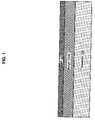
- FIG. 1illustrates a cross section of a silicon on insulator (SOI) substrate.
- SOI substratesare well known in the art to increase transistor performance by, among other features, reducing the capacitance that develops in a junction capacitance layer between impurity layers (e.g, impurity doped source and drain regions of a planar MOS structure) and a substrate.
- substrate 100comprises silicon.
- Atop substrate 100is a buried oxide 101 .
- the buried oxidecomprises silicon dioxide.
- Atop the buried oxide 101is silicon 102 .
- the SOI substratesgenerally include silicon 102 layers that are approximately 500 angstroms thick.
- An embodimentto further reduce the junction capacitance area, planarizes and polishes (e.g., by chemical mechanical polishing or CMP) the silicon 102 to approximately between 20 and 100 angstroms. It is to be understood, however, that the SOI combination of substrate 100 , buried oxide 101 and silicon 102 may also be prepared by separation by implanted oxygen (SIMOX), bonded and etched back (BESOI) or hydrogen implant before BESOI process (Smart Cut) as is understood in the art.
- SIMOXimplanted oxygen
- BESOIbonded and etched back
- Smart CutSmart Cut
- FIG. 2illustrates the substrate 100 cross section of FIG. 1 including strained silicon germanium 201 and silicon 202 prior to Smart Cut transfer of each to silicon 201 as is well known in the art and has been developed by SOITEC.
- a particular application of the Smart Cut methodinvolves growing a layer of strained silicon germanium 201 on silicon 202 as a separate substrate that includes a large sacrificial silicon 202 layer as illustrated by FIG. 2 .
- a high dose (i.e., 10 17 /cm 2 ) of hydrogenis implanted to a depth either in the silicon 202 adjacent to the strained silicon germanium 201 or to a depth within the silicon germanium layer 201 as illustrated by hydrogen implant 203 (shown deposited within silicon 202 ).
- the separate substrate comprised of silicon 202 and strained silicon germanium 201is brought into contact with the substrate 100 that includes buried oxide 101 and silicon 102 .
- the surfaces of silicon 102 and strained silicon germanium 201are joined by chemical hydrophobic bonding after a high temperature anneal.
- the strained silicon germanium 201bonds by covalent forces to the silicon 102 .
- the annealis approximately between 800° C. and 900° C. for approximately 1 hour.
- the annealfurther produces, based on the high dose hydrogen implant 203 in silicon 202 , an in-depth weakened layer of silicon 202 .
- the sacrificial portion of silicon 202(or of silicon germanium 201 and silicon 202 if the hydrogen implant 203 resides in the silicon germanium 201 ) can be cleaved, leaving behind the structure illustrated by FIG. 3 .
- the remaining silicon 202(or silicon germanium 201 ) may be chemically mechanically polished to form a suitable silicon 202 (or silicon germanium 201 ) surface for subsequent processing steps.
- Silicon and germaniumhave the same lattice structure; however, the lattice constant of germanium is 4.2% greater than the lattice constant of germanium (the lattice constant of silicon is 5.43 angstroms while the lattice constant of germanium is 5.66 angstroms).
- a silicon germanium alloy Si 1 ⁇ x Ge x , x0.0 to 1.0, has a monotonically increasing lattice constant a x increases from 0.0 to 1.0.
- Depositing a thin layer of silicon over silicon germaniumproduces, as the underlying silicon germanium lattice structure coerces the lattice thinly deposited layer of silicon, a silicon layer with tensile strain as the smaller silicon lattice aligns with the larger silicon germanium lattice.
- a thin silicon germanium layercan be grown with compressive strain on a layer of silicon. However, as the deposited layers of strained materials thicken, they tend to relax to their intrinsic lattice structure.
- FIG. 4illustrates the substrate 100 cross section of FIG. 3 following a high temperature, long duration anneal.
- the annealis approximately between 800° C. and 1100° C. for approximately 1 second to 3 hours.
- the temperatureis approximately 1000° C. and the duration is approximately 2 hours.
- the germanium in the strained silicon germanium 201diffuses into the silicon 102 and silicon 202 .
- the germaniumdiffuses to an approximate constant concentration throughout the strained silicon 201 , silicon 102 , and silicon 202 , it forms relaxed silicon germanium 401 .
- the lattice constant of the relaxed silicon germanium 401increases based on the germanium concentration in the relaxed silicon germanium 401 .
- the relaxed silicon germanium 401has a germanium concentration range of approximately 5% to 80% (i.e., approximately 5% to 80% of the silicon lattice sites are occupied by germanium). In an embodiment, the relaxed silicon germanium 401 has a germanium concentration approximately 15%.
- the relaxed silicon germanium 401may, based on the pre-anneal doping of silicon 102 , strained silicon germanium 201 , silicon 202 , or a combination thereof (or in an embodiment, a separate relaxed silicon germanium 401 doping process) may be p-doped with any p-dopant known in the art.
- the p-dopant concentration level of a relaxed silicon germanium 401 embodimentmay be approximately between undoped and 6*10 19 /cm 3 .
- the p-type dopant concentration level of relaxed silicon germanium 401is approximately 10 17 /cm 3 .
- FIG. 5illustrates a cross section of the substrate 100 of FIG. 4 following the lithographic patterning of the relaxed silicon germanium 401 to form a relaxed silicon germanium fin 501 .
- the relaxed silicon germanium fin 501may be patterned by any method known in the art to pattern silicon germanium. In an embodiment, the relaxed silicon germanium fin is patterned by any dry silicon etch process known in the art. Following the lithographic patterning, relaxed silicon germanium fin 501 of an embodiment has an approximately rectangular cross section as the lithographic patterning is substantially anisotropic and creates substantially vertical relaxed silicon germanium fin 501 sidewalls.
- the relaxed silicon germanium fin 501has a substantially trapezoidal cross section, with its top surface spanning a smaller lateral distance than its base adjacent to the buried oxide 101 .
- the relaxed silicon germanium fin 501comprises a top and two sidewalls whose width and height dimensions are approximately between 25% and 100% of the transistor gate length, and can have any shape from substantially tall and thin to substantially short and wide.
- the relaxed silicon germanium fin 501has other geometrical cross sections that may include additional sidewalls or may be substantially hemispherical.
- FIG. 6illustrates a cross section of the substrate 100 of FIG. 5 following the deposition of strained silicon 601 .
- the lattice constant of the relaxed silicon germanium fin 501is larger than the lattice constant of silicon.
- the silicon latticewill align with the relaxed silicon germanium fin 501 lattice to form strained silicon 601 .
- the relaxed silicon germanium fm 501 lattice constantis larger than that of silicon
- the subsequently formed strained silicon 601exhibits tensile strain as the smaller silicon lattice stretches to conform with the relaxed silicon germanium fin 501 lattice.
- the tensile strainincreases the carrier mobility in the strained silicon 601 that comprises the channel region of a non-planar MOS transistor of an embodiment.
- Strained silicon 601can be deposited by any method known in the art to deposit crystalline silicon.
- the strained silicon 601is deposited with selective epitaxy such that the silicon grows only on the surface of the relaxed silicon germanium fin 401 and not on the surface of the buried oxide 101 exposed during the pattering of relaxed silicon germanium fin 501 .
- a low pressure chemical vapor deposition process of an embodimentutilizes silane (SiH 4 ), disilane (Si 2 H 4 ), dichlorol silane (SiH 2 Cl 2 ), and trichlorol silane (SiHCl 3 ) as a silicon source and HCL as an etching gas for selective growth.
- the pressure of the deposition chamberis approximately between 500 millitorr and 500 torr
- the temperature of the substrate 100is approximately between 400° C. and 1100° C.
- the total precursor gas flow rateis approximately between 10 sccm and 1000 sccm. It is to be understood that the deposition conditions may vary depending on the size of the deposition chamber. It is to be further understood that the epitaxial deposition forms substantially a single crystal stained silicon 601 .
- the strained silicon 601is doped with a p-type dopant.
- the p-type dopant concentration level of strained silicon 601ranges from approximately undoped to 6*10 19 /cm 3 .
- the strained silicon 601may be doped by any doping method known in the art.
- the strained silicon 601may be doped in situ during its deposition by incorporating dopant precursors in the low pressure chemical deposition process of an embodiment.
- the strained silicon 601may alternatively be doped by out diffusion or implant.
- the cross section of the relaxed silicon germanium fin 501 of an embodimenthas a top and two sidewalls. It is important to note that the strained silicon 601 be deposited on the top and on both sidewalls of relaxed silicon germanium fin 501 with substantially uniform thickness for each surface.
- the strained silicon 601 of an embodiment on the top and sidewallshas a substantially uniform thickness of approximately between 2 nanometers and 10 nanometers In an embodiment, the strained silicon 601 thickness is approximately between 4 and 5 nanometers. In an embodiment, the strained silicon 601 thickness permits deeply depleted or fully depleted channel conditions as is understood in the art.
- FIG. 7illustrates a cross section of the substrate 100 of FIG. 6 following the deposition of a gate dielectric 701 and gate 702 to illustrate a non-planar, tri-gate transistor cross section.
- gate dielectric 701comprises silicon dioxide.
- gate dielectric 701comprises a high dielectric constant material like hafnium oxide, hafnium silicate, lanthanum oxide, lanthanum aluminate, zirconium oxide, zirconium silicate, tantalum oxide, titanium oxide, barium strontium titanate, barium titanate, strontium titanate, yttrium oxide, aluminum oxide, lead scandium tantanate, or lead zinc niobate.
- the gate dielectric 701may be deposited my any method known in the art to deposit a gate dielectric 701 material.
- the gate dielectric 701 depositionis a blanket deposition. Following the deposition of gate dielectric 701 , a gate 702 is deposited.
- the gate 702comprises polysilicon, polysilicon with a layer of metal at the high-k gate dielectric 701 interface, or a complete metal gate.
- the gate 702 depositionis a blanket deposition.
- eachis etched to expose areas of strained silicon 601 that will thereafter form the source and drain of the tri-gate non-planar transistor of an embodiment.
- the gate 702 and underlying gate dielectric 701 of an embodimentextend over all sides (in an embodiment, the top and both sidewalls) of the relaxed silicon germanium fin 501 including strained silicon 601 formed thereon.
- the gate 702is only adjacent to the. sidewalls of the relaxed silicon germanium fin 501 and does not extend across the top of the relaxed silicon germanium fin 501 .
- the strained silicon 601may be formed over the entire exposed surface (i.e., top and both sidewalls) of the relaxed silicon germanium fin 501 or may just be formed on the two sidewalls of the silicon germanium fin 501 .
- the gate dielectric 701may be formed over the entire exposed surface (i.e., top and both sidewalls) of the strained silicon 601 formed atop the relaxed silicon germanium fin 501 or may just be formed on the two sidewalls of strained silicon 601 .
- the non-planar transistor of an embodimentresembles a FinFET including strained silicon 601 channel regions.
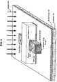
- FIG. 8is an illustration of a perspective view of the substrate 100 of FIG. 7 including buried oxide 101 , relaxed silicon germanium fin 501 , strained silicon 601 , gate dielectric 701 and gate 702 .
- the blanket deposition of gate dielectric 701 and gate 702have been etched to expose the relaxed silicon germanium fin 501 as described above. It is to be understood that one relaxed silicon germanium fin 501 can operate for many gates 702 and one gate 702 may operate with many relaxed silicon germanium fins 501 to create an array of non-planar, tri-gate MOS transistors.
- FIG. 9is an illustration of the perspective view of FIG. 8 including an implant 901 to form a source 902 and a drain 903 .
- the implant 901e.g., an n-type dopant implant for an NMOS device
- the implant 901further decreases the contact resistivity between both the source 902 and drain 903 with subsequently fabricated metal contacts to improve the performance of the non-planar, tri-gate MOS transistor of an embodiment.
- the resulting structure of an embodimentis a non-planar, tri-gate MOS transistor that includes a strained silicon 601 channel.
- the tensile strain on the strained silicon 601 latticeincreases the electron and hole mobility within the strained silicon 601 lattice to fabricate an NMOS device with improved performance characteristics.
- the strained silicon 601 thicknesspermits deeply depleted or fully depleted conditions to mitigate leakage current while the NMOS device is in an off state (i.e., enhancement mode with zero gate voltage).
Landscapes
- Thin Film Transistor (AREA)
- Insulated Gate Type Field-Effect Transistor (AREA)
- Metal-Oxide And Bipolar Metal-Oxide Semiconductor Integrated Circuits (AREA)
Abstract
Description
This is a Divisional Application of Ser. No. 11/039,197 filed Jan. 18, 2005 now U.S. Pat. No. 7,193,279.
Embodiments of the invention relate to a transistor structure and in particular to a non-planar transistor structure that incorporates a strained channel.
Traditional planar metal oxide semiconductor (MOS) transistor technology is approaching fundamental physical limits for certain transistor features past which it will be necessary to employ alternate materials, processing techniques, and/or transistor structure to support continued transistor performance improvement according to Moore's Law.
One such paradigm shift is a non-planar MOS structure. One particular non-planar MOS structure is a non-planar tri-gate transistor. A tri-gate transistor employs a three-dimensional gate structure that permits electrical signals to conduct along the top of the transistor gate and along both vertical sidewalls of the gate. The conduction along three sides of the gates enables, among other improvements, higher drive currents, faster switching speeds, and shorter gate lengths, simultaneously increasing the performance of the transistor while occupying less substrate area versus a planar MOS structure. The tri-gate structure further decreases the amount of current leakage, a problem to which ever shrinking planar MOS devices are prone, by improving the short channel characteristics of the transistor.
Another paradigm shift involves using strained semiconductor material for various portions of a transistor. Adding tensile or compressive strain to a semiconductor (depending on the particular application) lattice increases the carrier mobility within the strained semiconductor. In particular, for an NMOS device imparting tensile strain to a semiconductor increases the electron mobility (i.e., dominant charge carrier in an NMOS device). The increased carrier mobility in turn allows for higher drive current and corresponding faster switching speeds.
Embodiments of a non-planar MOS transistor structure with a strained channel region will be described. Reference will now be made in detail to a description of these embodiments as illustrated in the drawings. While the embodiments will be described in connection with these drawings, there is no intent to limit them to drawings disclosed herein. On the contrary, the intent is to cover all alternatives, modifications, and equivalents within the spirit and scope of the described embodiments as defined by the accompanying claims.
Simply stated, an embodiment is a non-planar MOS transistor structure including a strained channel region. The combination of a non-planar MOS transistor structure, and in particular an NMOS tri-gate transistor, with the benefits of a strained channel yields improved transistor drive current, switching speed, and decreased leakage current for a given gate length, gate width, and operating voltage versus a non-planar MOS structure with an unstrained channel or planar MOS structure including a strained channel.
Silicon and germanium have the same lattice structure; however, the lattice constant of germanium is 4.2% greater than the lattice constant of germanium (the lattice constant of silicon is 5.43 angstroms while the lattice constant of germanium is 5.66 angstroms). A silicon germanium alloy Si1−xGex, x=0.0 to 1.0, has a monotonically increasing lattice constant a x increases from 0.0 to 1.0. Depositing a thin layer of silicon over silicon germanium produces, as the underlying silicon germanium lattice structure coerces the lattice thinly deposited layer of silicon, a silicon layer with tensile strain as the smaller silicon lattice aligns with the larger silicon germanium lattice. Similarly, a thin silicon germanium layer can be grown with compressive strain on a layer of silicon. However, as the deposited layers of strained materials thicken, they tend to relax to their intrinsic lattice structure.
In an embodiment, thestrained silicon 601 is doped with a p-type dopant. In an embodiment the p-type dopant concentration level ofstrained silicon 601 ranges from approximately undoped to 6*1019/cm3. It is to be understood that thestrained silicon 601 may be doped by any doping method known in the art. In particular, thestrained silicon 601 may be doped in situ during its deposition by incorporating dopant precursors in the low pressure chemical deposition process of an embodiment. Thestrained silicon 601 may alternatively be doped by out diffusion or implant.
As noted, the cross section of the relaxedsilicon germanium fin 501 of an embodiment has a top and two sidewalls. It is important to note that thestrained silicon 601 be deposited on the top and on both sidewalls of relaxedsilicon germanium fin 501 with substantially uniform thickness for each surface. Thestrained silicon 601 of an embodiment on the top and sidewalls has a substantially uniform thickness of approximately between 2 nanometers and 10 nanometers In an embodiment, thestrained silicon 601 thickness is approximately between 4 and 5 nanometers. In an embodiment, thestrained silicon 601 thickness permits deeply depleted or fully depleted channel conditions as is understood in the art.
In an embodiment, thegate dielectric 701 deposition is a blanket deposition. Following the deposition ofgate dielectric 701, agate 702 is deposited. In an embodiment thegate 702 comprises polysilicon, polysilicon with a layer of metal at the high-k gate dielectric 701 interface, or a complete metal gate. In an embodiment, thegate 702 deposition is a blanket deposition. In an embodiment for which thegate dielectric 701 andgate 702 depositions are blanket depositions, each is etched to expose areas ofstrained silicon 601 that will thereafter form the source and drain of the tri-gate non-planar transistor of an embodiment. Of note is that thegate 702 andunderlying gate dielectric 701 of an embodiment extend over all sides (in an embodiment, the top and both sidewalls) of the relaxedsilicon germanium fin 501 includingstrained silicon 601 formed thereon.
In an alternate embodiment (not illustrated), thegate 702 is only adjacent to the. sidewalls of the relaxedsilicon germanium fin 501 and does not extend across the top of the relaxedsilicon germanium fin 501. Thestrained silicon 601 may be formed over the entire exposed surface (i.e., top and both sidewalls) of the relaxedsilicon germanium fin 501 or may just be formed on the two sidewalls of thesilicon germanium fin 501. Similarly, thegate dielectric 701 may be formed over the entire exposed surface (i.e., top and both sidewalls) of thestrained silicon 601 formed atop the relaxedsilicon germanium fin 501 or may just be formed on the two sidewalls ofstrained silicon 601. With such an arrangement, the non-planar transistor of an embodiment resembles a FinFET includingstrained silicon 601 channel regions.
The resulting structure of an embodiment is a non-planar, tri-gate MOS transistor that includes astrained silicon 601 channel. As noted, the tensile strain on thestrained silicon 601 lattice increases the electron and hole mobility within thestrained silicon 601 lattice to fabricate an NMOS device with improved performance characteristics. Further, in an embodiment, thestrained silicon 601 thickness permits deeply depleted or fully depleted conditions to mitigate leakage current while the NMOS device is in an off state (i.e., enhancement mode with zero gate voltage).
One skilled in the art will recognize the elegance of an embodiment as it combines a non-planar MOS transistor structure with a strained channel material to improve transistor performance.
Claims (3)
1. A method comprising:
providing a silicon film on an insulating substrate;
growing a silicon germanium film on a silicon substrate;
bonding the silicon germanium film to the silicon film of said insulating substrate;
removing a portion of said silicon substrate so as to leave a layer of silicon from said silicon substrate on said silicon germanium film on said insulating wafer;
annealing said insulating substrate so as to diffuse germanium from said silicon germanium film into said silicon film on said insulating substrate and into said layer of silicon from said silicon substrate so as to form a relaxed silicon germanium film from said silicon film on said insulating substrate, said silicon germanium film and said layer of silicon from said silicon substrate;
forming a fin having a top surface and two sidewalls from said relaxed said silicon germanium film;
forming a strained silicon layer on said top surface and said sidewalls of said fin;
forming a gate dielectric layer on said strained silicon layer; and
forming a gate electrode on said gate dielectric.
2. The method ofclaim 1 wherein said annealing produces a substantially uniform composition of germanium in said relaxed silicon germanium film.
3. The method ofclaim 1 wherein said strained silicon film is doped.
Priority Applications (1)
| Application Number | Priority Date | Filing Date | Title |
|---|---|---|---|
| US11/373,776US7531393B2 (en) | 2005-01-18 | 2006-03-09 | Non-planar MOS structure with a strained channel region |
Applications Claiming Priority (2)
| Application Number | Priority Date | Filing Date | Title |
|---|---|---|---|
| US11/039,197US7193279B2 (en) | 2005-01-18 | 2005-01-18 | Non-planar MOS structure with a strained channel region |
| US11/373,776US7531393B2 (en) | 2005-01-18 | 2006-03-09 | Non-planar MOS structure with a strained channel region |
Related Parent Applications (1)
| Application Number | Title | Priority Date | Filing Date |
|---|---|---|---|
| US11/039,197DivisionUS7193279B2 (en) | 2005-01-18 | 2005-01-18 | Non-planar MOS structure with a strained channel region |
Publications (2)
| Publication Number | Publication Date |
|---|---|
| US20060157794A1 US20060157794A1 (en) | 2006-07-20 |
| US7531393B2true US7531393B2 (en) | 2009-05-12 |
Family
ID=36295351
Family Applications (2)
| Application Number | Title | Priority Date | Filing Date |
|---|---|---|---|
| US11/039,197Expired - Fee RelatedUS7193279B2 (en) | 2005-01-18 | 2005-01-18 | Non-planar MOS structure with a strained channel region |
| US11/373,776Expired - Fee RelatedUS7531393B2 (en) | 2005-01-18 | 2006-03-09 | Non-planar MOS structure with a strained channel region |
Family Applications Before (1)
| Application Number | Title | Priority Date | Filing Date |
|---|---|---|---|
| US11/039,197Expired - Fee RelatedUS7193279B2 (en) | 2005-01-18 | 2005-01-18 | Non-planar MOS structure with a strained channel region |
Country Status (8)
| Country | Link |
|---|---|
| US (2) | US7193279B2 (en) |
| JP (1) | JP5408880B2 (en) |
| KR (1) | KR100903902B1 (en) |
| CN (1) | CN101142688B (en) |
| DE (1) | DE112006000229B4 (en) |
| GB (1) | GB2437867B (en) |
| TW (1) | TWI309091B (en) |
| WO (1) | WO2006078469A1 (en) |
Cited By (59)
| Publication number | Priority date | Publication date | Assignee | Title |
|---|---|---|---|---|
| US20080014721A1 (en)* | 2006-07-11 | 2008-01-17 | Matthias Bauer | Dual channel heterostructure |
| US20090079023A1 (en)* | 2007-09-24 | 2009-03-26 | Joerg Berthold | Method of fabricating an integrated circuit with stress enhancement |
| US8377783B2 (en) | 2010-09-30 | 2013-02-19 | Suvolta, Inc. | Method for reducing punch-through in a transistor device |
| US8400219B2 (en) | 2011-03-24 | 2013-03-19 | Suvolta, Inc. | Analog circuits having improved transistors, and methods therefor |
| US8404551B2 (en) | 2010-12-03 | 2013-03-26 | Suvolta, Inc. | Source/drain extension control for advanced transistors |
| US8421162B2 (en) | 2009-09-30 | 2013-04-16 | Suvolta, Inc. | Advanced transistors with punch through suppression |
| US8461875B1 (en) | 2011-02-18 | 2013-06-11 | Suvolta, Inc. | Digital circuits having improved transistors, and methods therefor |
| US8525271B2 (en) | 2011-03-03 | 2013-09-03 | Suvolta, Inc. | Semiconductor structure with improved channel stack and method for fabrication thereof |
| US8569156B1 (en) | 2011-05-16 | 2013-10-29 | Suvolta, Inc. | Reducing or eliminating pre-amorphization in transistor manufacture |
| US8569128B2 (en) | 2010-06-21 | 2013-10-29 | Suvolta, Inc. | Semiconductor structure and method of fabrication thereof with mixed metal types |
| US8599623B1 (en) | 2011-12-23 | 2013-12-03 | Suvolta, Inc. | Circuits and methods for measuring circuit elements in an integrated circuit device |
| US8614128B1 (en) | 2011-08-23 | 2013-12-24 | Suvolta, Inc. | CMOS structures and processes based on selective thinning |
| US8629016B1 (en) | 2011-07-26 | 2014-01-14 | Suvolta, Inc. | Multiple transistor types formed in a common epitaxial layer by differential out-diffusion from a doped underlayer |
| US8637955B1 (en) | 2012-08-31 | 2014-01-28 | Suvolta, Inc. | Semiconductor structure with reduced junction leakage and method of fabrication thereof |
| US8645878B1 (en) | 2011-08-23 | 2014-02-04 | Suvolta, Inc. | Porting a circuit design from a first semiconductor process to a second semiconductor process |
| US8713511B1 (en) | 2011-09-16 | 2014-04-29 | Suvolta, Inc. | Tools and methods for yield-aware semiconductor manufacturing process target generation |
| US8735987B1 (en) | 2011-06-06 | 2014-05-27 | Suvolta, Inc. | CMOS gate stack structures and processes |
| US8748986B1 (en) | 2011-08-05 | 2014-06-10 | Suvolta, Inc. | Electronic device with controlled threshold voltage |
| US8748270B1 (en) | 2011-03-30 | 2014-06-10 | Suvolta, Inc. | Process for manufacturing an improved analog transistor |
| US8796048B1 (en) | 2011-05-11 | 2014-08-05 | Suvolta, Inc. | Monitoring and measurement of thin film layers |
| US8811068B1 (en) | 2011-05-13 | 2014-08-19 | Suvolta, Inc. | Integrated circuit devices and methods |
| US8819603B1 (en) | 2011-12-15 | 2014-08-26 | Suvolta, Inc. | Memory circuits and methods of making and designing the same |
| US8816754B1 (en) | 2012-11-02 | 2014-08-26 | Suvolta, Inc. | Body bias circuits and methods |
| US8863064B1 (en) | 2012-03-23 | 2014-10-14 | Suvolta, Inc. | SRAM cell layout structure and devices therefrom |
| US8877619B1 (en) | 2012-01-23 | 2014-11-04 | Suvolta, Inc. | Process for manufacture of integrated circuits with different channel doping transistor architectures and devices therefrom |
| US8883600B1 (en) | 2011-12-22 | 2014-11-11 | Suvolta, Inc. | Transistor having reduced junction leakage and methods of forming thereof |
| US8895327B1 (en) | 2011-12-09 | 2014-11-25 | Suvolta, Inc. | Tipless transistors, short-tip transistors, and methods and circuits therefor |
| US8951850B1 (en) | 2013-08-21 | 2015-02-10 | International Business Machines Corporation | FinFET formed over dielectric |
| US8970289B1 (en) | 2012-01-23 | 2015-03-03 | Suvolta, Inc. | Circuits and devices for generating bi-directional body bias voltages, and methods therefor |
| US8976575B1 (en) | 2013-08-29 | 2015-03-10 | Suvolta, Inc. | SRAM performance monitor |
| US8988153B1 (en) | 2013-03-09 | 2015-03-24 | Suvolta, Inc. | Ring oscillator with NMOS or PMOS variation insensitivity |
| US8995204B2 (en) | 2011-06-23 | 2015-03-31 | Suvolta, Inc. | Circuit devices and methods having adjustable transistor body bias |
| US8994415B1 (en) | 2013-03-01 | 2015-03-31 | Suvolta, Inc. | Multiple VDD clock buffer |
| US8999861B1 (en) | 2011-05-11 | 2015-04-07 | Suvolta, Inc. | Semiconductor structure with substitutional boron and method for fabrication thereof |
| US9041126B2 (en) | 2012-09-21 | 2015-05-26 | Mie Fujitsu Semiconductor Limited | Deeply depleted MOS transistors having a screening layer and methods thereof |
| US9054219B1 (en) | 2011-08-05 | 2015-06-09 | Mie Fujitsu Semiconductor Limited | Semiconductor devices having fin structures and fabrication methods thereof |
| US9070477B1 (en) | 2012-12-12 | 2015-06-30 | Mie Fujitsu Semiconductor Limited | Bit interleaved low voltage static random access memory (SRAM) and related methods |
| US9093997B1 (en) | 2012-11-15 | 2015-07-28 | Mie Fujitsu Semiconductor Limited | Slew based process and bias monitors and related methods |
| US9093550B1 (en) | 2012-01-31 | 2015-07-28 | Mie Fujitsu Semiconductor Limited | Integrated circuits having a plurality of high-K metal gate FETs with various combinations of channel foundation structure and gate stack structure and methods of making same |
| US20150228755A1 (en)* | 2014-02-11 | 2015-08-13 | GlobalFoundries, Inc. | Integrated circuits with relaxed silicon / germanium fins |
| US9112057B1 (en) | 2012-09-18 | 2015-08-18 | Mie Fujitsu Semiconductor Limited | Semiconductor devices with dopant migration suppression and method of fabrication thereof |
| US9112484B1 (en) | 2012-12-20 | 2015-08-18 | Mie Fujitsu Semiconductor Limited | Integrated circuit process and bias monitors and related methods |
| US9112495B1 (en) | 2013-03-15 | 2015-08-18 | Mie Fujitsu Semiconductor Limited | Integrated circuit device body bias circuits and methods |
| US20150255555A1 (en)* | 2014-03-05 | 2015-09-10 | Globalfoundries Inc. | Methods of forming a non-planar ultra-thin body device |
| US9236466B1 (en) | 2011-10-07 | 2016-01-12 | Mie Fujitsu Semiconductor Limited | Analog circuits having improved insulated gate transistors, and methods therefor |
| US9268885B1 (en) | 2013-02-28 | 2016-02-23 | Mie Fujitsu Semiconductor Limited | Integrated circuit device methods and models with predicted device metric variations |
| US9299801B1 (en) | 2013-03-14 | 2016-03-29 | Mie Fujitsu Semiconductor Limited | Method for fabricating a transistor device with a tuned dopant profile |
| US9299698B2 (en) | 2012-06-27 | 2016-03-29 | Mie Fujitsu Semiconductor Limited | Semiconductor structure with multiple transistors having various threshold voltages |
| US9319013B2 (en) | 2014-08-19 | 2016-04-19 | Mie Fujitsu Semiconductor Limited | Operational amplifier input offset correction with transistor threshold voltage adjustment |
| US9406567B1 (en) | 2012-02-28 | 2016-08-02 | Mie Fujitsu Semiconductor Limited | Method for fabricating multiple transistor devices on a substrate with varying threshold voltages |
| US9431068B2 (en) | 2012-10-31 | 2016-08-30 | Mie Fujitsu Semiconductor Limited | Dynamic random access memory (DRAM) with low variation transistor peripheral circuits |
| US9443963B2 (en) | 2014-04-07 | 2016-09-13 | International Business Machines Corporation | SiGe FinFET with improved junction doping control |
| US9449967B1 (en) | 2013-03-15 | 2016-09-20 | Fujitsu Semiconductor Limited | Transistor array structure |
| US9478571B1 (en) | 2013-05-24 | 2016-10-25 | Mie Fujitsu Semiconductor Limited | Buried channel deeply depleted channel transistor |
| US9710006B2 (en) | 2014-07-25 | 2017-07-18 | Mie Fujitsu Semiconductor Limited | Power up body bias circuits and methods |
| US9871139B2 (en)* | 2016-05-23 | 2018-01-16 | Samsung Electronics Co., Ltd. | Sacrificial epitaxial gate stressors |
| US9985030B2 (en) | 2014-04-07 | 2018-05-29 | International Business Machines Corporation | FinFET semiconductor device having integrated SiGe fin |
| US10074568B2 (en) | 2009-09-30 | 2018-09-11 | Mie Fujitsu Semiconductor Limited | Electronic devices and systems, and methods for making and using same |
| US10692973B2 (en)* | 2017-04-01 | 2020-06-23 | Intel Corporation | Germanium-rich channel transistors including one or more dopant diffusion barrier elements |
Families Citing this family (84)
| Publication number | Priority date | Publication date | Assignee | Title |
|---|---|---|---|---|
| US6909151B2 (en) | 2003-06-27 | 2005-06-21 | Intel Corporation | Nonplanar device with stress incorporation layer and method of fabrication |
| KR100625175B1 (en)* | 2004-05-25 | 2006-09-20 | 삼성전자주식회사 | Semiconductor device having channel layer and method of manufacturing same |
| US7422946B2 (en) | 2004-09-29 | 2008-09-09 | Intel Corporation | Independently accessed double-gate and tri-gate transistors in same process flow |
| US20060086977A1 (en) | 2004-10-25 | 2006-04-27 | Uday Shah | Nonplanar device with thinned lower body portion and method of fabrication |
| US7470951B2 (en)* | 2005-01-31 | 2008-12-30 | Freescale Semiconductor, Inc. | Hybrid-FET and its application as SRAM |
| FR2881877B1 (en)* | 2005-02-04 | 2007-08-31 | Soitec Silicon On Insulator | MULTI-LAYER CHANNEL FIELD EFFECT TRANSISTOR WITH MULTI-LAYER CHANNEL |
| US7518196B2 (en) | 2005-02-23 | 2009-04-14 | Intel Corporation | Field effect transistor with narrow bandgap source and drain regions and method of fabrication |
| US7538351B2 (en)* | 2005-03-23 | 2009-05-26 | Taiwan Semiconductor Manufacturing Co., Ltd. | Method for forming an SOI structure with improved carrier mobility and ESD protection |
| FR2885733B1 (en)* | 2005-05-16 | 2008-03-07 | St Microelectronics Crolles 2 | THREE-GRID TRANSISTOR STRUCTURE |
| US7858481B2 (en) | 2005-06-15 | 2010-12-28 | Intel Corporation | Method for fabricating transistor with thinned channel |
| US7960791B2 (en)* | 2005-06-24 | 2011-06-14 | International Business Machines Corporation | Dense pitch bulk FinFET process by selective EPI and etch |
| US7400031B2 (en)* | 2005-09-19 | 2008-07-15 | International Business Machines Corporation | Asymmetrically stressed CMOS FinFET |
| US7452768B2 (en)* | 2005-10-25 | 2008-11-18 | Freescale Semiconductor, Inc. | Multiple device types including an inverted-T channel transistor and method therefor |
| US8513066B2 (en)* | 2005-10-25 | 2013-08-20 | Freescale Semiconductor, Inc. | Method of making an inverted-T channel transistor |
| US7615806B2 (en) | 2005-10-31 | 2009-11-10 | Freescale Semiconductor, Inc. | Method for forming a semiconductor structure and structure thereof |
| US7575975B2 (en)* | 2005-10-31 | 2009-08-18 | Freescale Semiconductor, Inc. | Method for forming a planar and vertical semiconductor structure having a strained semiconductor layer |
| US7341916B2 (en)* | 2005-11-10 | 2008-03-11 | Atmel Corporation | Self-aligned nanometer-level transistor defined without lithography |
| KR100734304B1 (en)* | 2006-01-16 | 2007-07-02 | 삼성전자주식회사 | Manufacturing method of transistor |
| EP1833094B1 (en)* | 2006-03-06 | 2011-02-02 | STMicroelectronics (Crolles 2) SAS | Formation of shallow SiGe conduction channel |
| JP2007299951A (en)* | 2006-04-28 | 2007-11-15 | Toshiba Corp | Semiconductor device and manufacturing method thereof |
| US7999251B2 (en)* | 2006-09-11 | 2011-08-16 | International Business Machines Corporation | Nanowire MOSFET with doped epitaxial contacts for source and drain |
| US7452758B2 (en)* | 2007-03-14 | 2008-11-18 | International Business Machines Corporation | Process for making FinFET device with body contact and buried oxide junction isolation |
| US7821061B2 (en)* | 2007-03-29 | 2010-10-26 | Intel Corporation | Silicon germanium and germanium multigate and nanowire structures for logic and multilevel memory applications |
| CN100570823C (en)* | 2007-11-06 | 2009-12-16 | 清华大学 | A Method for Obtaining Low Dislocation Density Epitaxial Thin Films Using Necked Epitaxy |
| US7629643B2 (en)* | 2007-11-30 | 2009-12-08 | Intel Corporation | Independent n-tips for multi-gate transistors |
| KR100920047B1 (en)* | 2007-12-20 | 2009-10-07 | 주식회사 하이닉스반도체 | Vertical transistors and their formation |
| US8129749B2 (en)* | 2008-03-28 | 2012-03-06 | Intel Corporation | Double quantum well structures for transistors |
| US8278687B2 (en)* | 2008-03-28 | 2012-10-02 | Intel Corporation | Semiconductor heterostructures to reduce short channel effects |
| KR101505494B1 (en)* | 2008-04-30 | 2015-03-24 | 한양대학교 산학협력단 | Cap-less memory device |
| US8362566B2 (en) | 2008-06-23 | 2013-01-29 | Intel Corporation | Stress in trigate devices using complimentary gate fill materials |
| US8053838B2 (en)* | 2008-06-26 | 2011-11-08 | International Business Machines Corporation | Structures, fabrication methods, design structures for strained fin field effect transistors (FinFets) |
| US7833891B2 (en)* | 2008-07-23 | 2010-11-16 | International Business Machines Corporation | Semiconductor device manufacturing method using oxygen diffusion barrier layer between buried oxide layer and high K dielectric layer |
| US7884354B2 (en)* | 2008-07-31 | 2011-02-08 | Intel Corporation | Germanium on insulator (GOI) semiconductor substrates |
| US7781283B2 (en)* | 2008-08-15 | 2010-08-24 | International Business Machines Corporation | Split-gate DRAM with MuGFET, design structure, and method of manufacture |
| US7979836B2 (en)* | 2008-08-15 | 2011-07-12 | International Business Machines Corporation | Split-gate DRAM with MuGFET, design structure, and method of manufacture |
| US8237195B2 (en)* | 2008-09-29 | 2012-08-07 | Fairchild Semiconductor Corporation | Power MOSFET having a strained channel in a semiconductor heterostructure on metal substrate |
| US8184472B2 (en)* | 2009-03-13 | 2012-05-22 | International Business Machines Corporation | Split-gate DRAM with lateral control-gate MuGFET |
| JP5645368B2 (en)* | 2009-04-14 | 2014-12-24 | 株式会社日立製作所 | Semiconductor device and manufacturing method thereof |
| KR101089659B1 (en) | 2009-06-03 | 2011-12-06 | 서울대학교산학협력단 | Memory cell having a protruding body as a storage node and a method of manufacturing the same |
| CN102640269B (en)* | 2009-09-30 | 2015-08-12 | 苏沃塔公司 | Electronic installation and system and production and preparation method thereof |
| US8021949B2 (en)* | 2009-12-01 | 2011-09-20 | International Business Machines Corporation | Method and structure for forming finFETs with multiple doping regions on a same chip |
| US8440998B2 (en) | 2009-12-21 | 2013-05-14 | Intel Corporation | Increasing carrier injection velocity for integrated circuit devices |
| US8633470B2 (en)* | 2009-12-23 | 2014-01-21 | Intel Corporation | Techniques and configurations to impart strain to integrated circuit devices |
| US8530286B2 (en) | 2010-04-12 | 2013-09-10 | Suvolta, Inc. | Low power semiconductor transistor structure and method of fabrication thereof |
| US8759872B2 (en) | 2010-06-22 | 2014-06-24 | Suvolta, Inc. | Transistor with threshold voltage set notch and method of fabrication thereof |
| CN102468303B (en)* | 2010-11-10 | 2015-05-13 | 中国科学院微电子研究所 | Semiconductor memory cell, device and preparation method thereof |
| TWI499006B (en)* | 2011-10-07 | 2015-09-01 | Etron Technology Inc | Dynamic memory structure |
| CN103137671B (en)* | 2011-12-02 | 2015-06-24 | 中芯国际集成电路制造(上海)有限公司 | Multi-grid field effect transistor and manufacturing method thereof |
| KR101835655B1 (en) | 2012-03-06 | 2018-03-07 | 삼성전자주식회사 | FinFET and method of fabricating the same |
| US8872284B2 (en)* | 2012-03-20 | 2014-10-28 | Taiwan Semiconductor Manufacturing Company, Ltd. | FinFET with metal gate stressor |
| CN103367432B (en)* | 2012-03-31 | 2016-02-03 | 中芯国际集成电路制造(上海)有限公司 | Multiple gate field effect transistor and manufacture method thereof |
| CN103515209B (en)* | 2012-06-19 | 2017-07-14 | 中芯国际集成电路制造(上海)有限公司 | Fin field effect pipe and forming method thereof |
| CN103515420B (en)* | 2012-06-26 | 2016-06-29 | 中芯国际集成电路制造(上海)有限公司 | Semiconductor device and forming method thereof |
| US9136383B2 (en) | 2012-08-09 | 2015-09-15 | Taiwan Semiconductor Manufacturing Company, Ltd. | Contact structure of semiconductor device |
| US9817928B2 (en) | 2012-08-31 | 2017-11-14 | Synopsys, Inc. | Latch-up suppression and substrate noise coupling reduction through a substrate back-tie for 3D integrated circuits |
| US9190346B2 (en) | 2012-08-31 | 2015-11-17 | Synopsys, Inc. | Latch-up suppression and substrate noise coupling reduction through a substrate back-tie for 3D integrated circuits |
| US9379018B2 (en) | 2012-12-17 | 2016-06-28 | Synopsys, Inc. | Increasing Ion/Ioff ratio in FinFETs and nano-wires |
| US8847324B2 (en) | 2012-12-17 | 2014-09-30 | Synopsys, Inc. | Increasing ION /IOFF ratio in FinFETs and nano-wires |
| US8957476B2 (en) | 2012-12-20 | 2015-02-17 | Intel Corporation | Conversion of thin transistor elements from silicon to silicon germanium |
| CN103915483B (en)* | 2012-12-28 | 2019-06-14 | 瑞萨电子株式会社 | Field effect transistor with channel core modified to reduce leakage current and method of making |
| US8951870B2 (en)* | 2013-03-14 | 2015-02-10 | International Business Machines Corporation | Forming strained and relaxed silicon and silicon germanium fins on the same wafer |
| GB2549911A (en)* | 2013-06-26 | 2017-11-01 | Intel Corp | Conversion of thin transistor elements from silicon to silicon germanium |
| CN103413828A (en)* | 2013-07-18 | 2013-11-27 | 清华大学 | Polygon channel layer multiple-grid structure tunneling transistor and forming method thereof |
| US8952420B1 (en) | 2013-07-29 | 2015-02-10 | Stmicroelectronics, Inc. | Method to induce strain in 3-D microfabricated structures |
| US9496397B2 (en) | 2013-08-20 | 2016-11-15 | Taiwan Semiconductor Manufacturing Co., Ltd. | FinFet device with channel epitaxial region |
| US9099559B2 (en) | 2013-09-16 | 2015-08-04 | Stmicroelectronics, Inc. | Method to induce strain in finFET channels from an adjacent region |
| JP6235325B2 (en)* | 2013-12-10 | 2017-11-22 | 株式会社東芝 | Field effect transistor and manufacturing method thereof, semiconductor device and manufacturing method thereof |
| KR102145262B1 (en)* | 2013-12-16 | 2020-08-18 | 인텔 코포레이션 | Dual strained cladding layers for semiconductor devices |
| KR101628197B1 (en) | 2014-08-22 | 2016-06-09 | 삼성전자주식회사 | Method of fabricating the semiconductor device |
| KR102255174B1 (en)* | 2014-10-10 | 2021-05-24 | 삼성전자주식회사 | Semiconductor device having active region and method of forming the same |
| WO2016060337A1 (en)* | 2014-10-13 | 2016-04-21 | 한국과학기술원 | Field effect transistor manufacturing method |
| US9614057B2 (en)* | 2014-12-30 | 2017-04-04 | International Business Machines Corporation | Enriched, high mobility strained fin having bottom dielectric isolation |
| US9543323B2 (en)* | 2015-01-13 | 2017-01-10 | International Business Machines Corporation | Strain release in PFET regions |
| KR102310080B1 (en)* | 2015-03-02 | 2021-10-12 | 삼성전자주식회사 | Semiconductor devices and methods of manufacturing semiconductor devices |
| US9954107B2 (en) | 2015-05-05 | 2018-04-24 | International Business Machines Corporation | Strained FinFET source drain isolation |
| US9607901B2 (en) | 2015-05-06 | 2017-03-28 | Stmicroelectronics, Inc. | Integrated tensile strained silicon NFET and compressive strained silicon-germanium PFET implemented in FINFET technology |
| FR3036847A1 (en)* | 2015-05-27 | 2016-12-02 | St Microelectronics Crolles 2 Sas | METHOD FOR MAKING MOS TRANSISTORS WITH INCREASED CHANNEL WIDTH FROM SOI-TYPE SUBSTRATE, ESPECIALLY FDSOI, AND CORRESPONDING INTEGRATED CIRCUIT |
| US10833175B2 (en)* | 2015-06-04 | 2020-11-10 | International Business Machines Corporation | Formation of dislocation-free SiGe finFET using porous silicon |
| US9680018B2 (en)* | 2015-09-21 | 2017-06-13 | International Business Machines Corporation | Method of forming high-germanium content silicon germanium alloy fins on insulator |
| US9601385B1 (en)* | 2016-01-27 | 2017-03-21 | International Business Machines Corporation | Method of making a dual strained channel semiconductor device |
| US9748404B1 (en)* | 2016-02-29 | 2017-08-29 | International Business Machines Corporation | Method for fabricating a semiconductor device including gate-to-bulk substrate isolation |
| CN108010880A (en)* | 2016-10-31 | 2018-05-08 | 中芯国际集成电路制造(上海)有限公司 | Semiconductor device and its manufacture method |
| WO2020150482A1 (en)* | 2019-01-16 | 2020-07-23 | The Regents Of The University Of California | Wafer bonding for embedding active regions with relaxed nanofeatures |
| CN111509048A (en)* | 2020-04-28 | 2020-08-07 | 上海华力集成电路制造有限公司 | N-type fin transistor and its manufacturing method |
Citations (88)
| Publication number | Priority date | Publication date | Assignee | Title |
|---|---|---|---|---|
| US5124777A (en) | 1990-07-02 | 1992-06-23 | Samsung Electronics Co., Ltd. | Dielectric medium for capacitor of semiconductor device |
| US5338959A (en) | 1992-03-30 | 1994-08-16 | Samsung Electronics Co., Ltd. | Thin film transistor with three dimensional multichannel structure |
| US5346839A (en) | 1991-06-10 | 1994-09-13 | Texas Instruments Incorporated | Sidewall doping technique for SOI transistors |
| EP0623963A1 (en) | 1993-05-06 | 1994-11-09 | Siemens Aktiengesellschaft | MOSFET on SOI substrate |
| US5466621A (en) | 1988-11-21 | 1995-11-14 | Hitachi, Ltd. | Method of manufacturing a semiconductor device having silicon islands |
| US5545586A (en) | 1990-11-27 | 1996-08-13 | Nec Corporation | Method of making a transistor having easily controllable impurity profile |
| US5563077A (en) | 1992-04-24 | 1996-10-08 | Hyundai Electronics Industries Co., Ltd. | Method of fabricating a thin film transistor having vertical channel |
| US5578513A (en) | 1993-09-17 | 1996-11-26 | Mitsubishi Denki Kabushiki Kaisha | Method of making a semiconductor device having a gate all around type of thin film transistor |
| US5658806A (en) | 1995-10-26 | 1997-08-19 | National Science Council | Method for fabricating thin-film transistor with bottom-gate or dual-gate configuration |
| US5701016A (en) | 1994-11-24 | 1997-12-23 | Kabushiki Kaisha Toshiba | Semiconductor device and method for its manufacture |
| US5716879A (en) | 1994-12-15 | 1998-02-10 | Goldstar Electron Company, Ltd. | Method of making a thin film transistor |
| US5827769A (en) | 1996-11-20 | 1998-10-27 | Intel Corporation | Method for fabricating a transistor with increased hot carrier resistance by nitridizing and annealing the sidewall oxide of the gate electrode |
| US5905285A (en) | 1996-09-12 | 1999-05-18 | Advanced Micro Devices, Inc. | Ultra short trench transistors and process for making same |
| US6251751B1 (en) | 1997-10-16 | 2001-06-26 | International Business Machines Corporation | Bulk and strained silicon on insulator using local selective oxidation |
| US6252284B1 (en) | 1999-12-09 | 2001-06-26 | International Business Machines Corporation | Planarized silicon fin device |
| US20020011612A1 (en) | 2000-07-31 | 2002-01-31 | Kabushiki Kaisha Toshiba | Semiconductor device and method for manufacturing the same |
| US20020036290A1 (en) | 2000-09-28 | 2002-03-28 | Kabushiki Kaisha Toshiba | Semiconductor device having MIS field effect transistors or three-dimensional structure |
| US6376317B1 (en) | 1998-03-30 | 2002-04-23 | Micron Technology, Inc. | Methods for dual-gated transistors |
| EP1202335A2 (en) | 2000-10-18 | 2002-05-02 | International Business Machines Corporation | Method of fabricating semiconductor side wall fin |
| US6396108B1 (en) | 2000-11-13 | 2002-05-28 | Advanced Micro Devices, Inc. | Self-aligned double gate silicon-on-insulator (SOI) device |
| WO2002043151A1 (en) | 2000-11-22 | 2002-05-30 | Hitachi, Ltd | Semiconductor device and method for fabricating the same |
| US20020081794A1 (en) | 2000-12-26 | 2002-06-27 | Nec Corporation | Enhanced deposition control in fabricating devices in a semiconductor wafer |
| US6413802B1 (en) | 2000-10-23 | 2002-07-02 | The Regents Of The University Of California | Finfet transistor structures having a double gate channel extending vertically from a substrate and methods of manufacture |
| US6475869B1 (en) | 2001-02-26 | 2002-11-05 | Advanced Micro Devices, Inc. | Method of forming a double gate transistor having an epitaxial silicon/germanium channel region |
| US6475890B1 (en) | 2001-02-12 | 2002-11-05 | Advanced Micro Devices, Inc. | Fabrication of a field effect transistor with an upside down T-shaped semiconductor pillar in SOI technology |
| US20020166838A1 (en) | 2001-05-10 | 2002-11-14 | Institute Of Microelectronics | Sloped trench etching process |
| US20020167007A1 (en) | 1998-12-29 | 2002-11-14 | Semiconductor Energy Laboratory Co., Ltd. | Semiconductor device and method of fabricating the same |
| US6483156B1 (en) | 2000-03-16 | 2002-11-19 | International Business Machines Corporation | Double planar gated SOI MOSFET structure |
| US20030057486A1 (en) | 2001-09-27 | 2003-03-27 | International Business Machines Corporation | Fin field effect transistor with self-aligned gate |
| US20030085194A1 (en) | 2001-11-07 | 2003-05-08 | Hopkins Dean A. | Method for fabricating close spaced mirror arrays |
| US6562665B1 (en) | 2000-10-16 | 2003-05-13 | Advanced Micro Devices, Inc. | Fabrication of a field effect transistor with a recess in a semiconductor pillar in SOI technology |
| US20030098488A1 (en) | 2001-11-27 | 2003-05-29 | O'keeffe James | Band-structure modulation of nano-structures in an electric field |
| US20030102497A1 (en) | 2001-12-04 | 2003-06-05 | International Business Machines Corporation | Multiple-plane finFET CMOS |
| US20030111686A1 (en) | 2001-12-13 | 2003-06-19 | Nowak Edward J. | Method for forming asymmetric dual gate transistor |
| US20030122186A1 (en) | 2001-03-13 | 2003-07-03 | Nat'l. Inst. Of Advanced Indust'l Sci. And Tech. | Double-gate field-effect transistor, integrated circuit using the transistor and method of manufacturing the same |
| US20030143791A1 (en) | 2002-01-29 | 2003-07-31 | Samsung Electronics Co., Ltd. | Methods for fabricating MOS transistors with notched gate electrodes |
| US20030151077A1 (en) | 2002-02-13 | 2003-08-14 | Leo Mathew | Method of forming a vertical double gate semiconductor device and structure thereof |
| US6611029B1 (en) | 2002-11-08 | 2003-08-26 | Advanced Micro Devices, Inc. | Double gate semiconductor device having separate gates |
| JP2003298051A (en) | 2002-01-30 | 2003-10-17 | Soko Lee | Double gate FET device and method of manufacturing the same |
| US6635909B2 (en) | 2002-03-19 | 2003-10-21 | International Business Machines Corporation | Strained fin FETs structure and method |
| US6645797B1 (en) | 2002-12-06 | 2003-11-11 | Advanced Micro Devices, Inc. | Method for forming fins in a FinFET device using sacrificial carbon layer |
| US20030227036A1 (en) | 2002-02-22 | 2003-12-11 | Naoharu Sugiyama | Semiconductor device |
| US6680240B1 (en) | 2002-06-25 | 2004-01-20 | Advanced Micro Devices, Inc. | Silicon-on-insulator device with strained device film and method for making the same with partial replacement of isolation oxide |
| US20040031979A1 (en) | 2002-06-07 | 2004-02-19 | Amberwave Systems Corporation | Strained-semiconductor-on-insulator device structures |
| US20040036127A1 (en) | 2002-08-23 | 2004-02-26 | Chau Robert S. | Tri-gate devices and methods of fabrication |
| US20040036118A1 (en) | 2002-08-26 | 2004-02-26 | International Business Machines Corporation | Concurrent Fin-FET and thick-body device fabrication |
| US6706571B1 (en) | 2002-10-22 | 2004-03-16 | Advanced Micro Devices, Inc. | Method for forming multiple structures in a semiconductor device |
| US6709982B1 (en) | 2002-11-26 | 2004-03-23 | Advanced Micro Devices, Inc. | Double spacer FinFET formation |
| US20040061178A1 (en) | 2002-09-30 | 2004-04-01 | Advanced Micro Devices Inc. | Finfet having improved carrier mobility and method of its formation |
| US6716690B1 (en) | 2003-03-12 | 2004-04-06 | Advanced Micro Devices, Inc. | Uniformly doped source/drain junction in a double-gate MOSFET |
| US6716684B1 (en) | 2000-11-13 | 2004-04-06 | Advanced Micro Devices, Inc. | Method of making a self-aligned triple gate silicon-on-insulator device |
| US6730964B2 (en) | 1997-07-22 | 2004-05-04 | Hitachi, Ltd. | Semiconductor device and method of producing the same |
| US20040092067A1 (en) | 2001-05-24 | 2004-05-13 | International Business Machines Corporation | Damascene double-gate MOSFET with vertical channel regions |
| US20040092062A1 (en) | 2002-11-08 | 2004-05-13 | Ahmed Shibly S. | Planarizing gate material to improve gate critical dimension in semiconductor devices |
| US20040110097A1 (en) | 2002-12-06 | 2004-06-10 | Ahmed Shibly S. | Double gate semiconductor device having a metal gate |
| US20040119100A1 (en) | 2002-12-19 | 2004-06-24 | International Business Machines Corporation | Dense dual-plane devices |
| US6756657B1 (en) | 1993-06-25 | 2004-06-29 | Semiconductor Energy Laboratory Co., Ltd. | Method of preparing a semiconductor having controlled crystal orientation |
| WO2004059726A1 (en) | 2002-12-20 | 2004-07-15 | International Business Machines Corporation | Integrated antifuse structure for finfet and cmos devices |
| US6764884B1 (en) | 2003-04-03 | 2004-07-20 | Advanced Micro Devices, Inc. | Method for forming a gate in a FinFET device and thinning a fin in a channel region of the FinFET device |
| US20040145019A1 (en) | 2003-01-23 | 2004-07-29 | Srikanteswara Dakshina-Murthy | Strained channel finfet |
| US20040166642A1 (en) | 2003-02-20 | 2004-08-26 | Hao-Yu Chen | Semiconductor nano-rod devices |
| US20040173846A1 (en) | 2003-03-05 | 2004-09-09 | Hergenrother John Michael | Diffused MOS devices with strained silicon portions and methods for forming same |
| US20040173815A1 (en) | 2003-03-04 | 2004-09-09 | Yee-Chia Yeo | Strained-channel transistor structure with lattice-mismatched zone |
| US20040180491A1 (en) | 2003-03-13 | 2004-09-16 | Nobutoshi Arai | Memory function body, particle forming method therefor and, memory device, semiconductor device, and electronic equipment having the memory function body |
| US20040191980A1 (en) | 2003-03-27 | 2004-09-30 | Rafael Rios | Multi-corner FET for better immunity from short channel effects |
| US20040198003A1 (en) | 2003-03-26 | 2004-10-07 | Taiwan Semiconductor Manufacturing Co., Ltd. | Multiple-gate transistors with improved gate control |
| US20040195624A1 (en) | 2003-04-04 | 2004-10-07 | National Taiwan University | Strained silicon fin field effect transistor |
| US20040227187A1 (en) | 2003-02-13 | 2004-11-18 | Zhiyuan Cheng | Integrated semiconductor device and method to make same |
| US20040238887A1 (en) | 2001-07-05 | 2004-12-02 | Fumiyuki Nihey | Field-effect transistor constituting channel by carbon nano tubes |
| US20040253792A1 (en) | 2003-06-13 | 2004-12-16 | International Business Machines Corporation | Strained-silicon-on-insulator single-and double-gate MOSFET and method for forming the same |
| US20040256647A1 (en) | 2003-06-23 | 2004-12-23 | Sharp Laboratories Of America Inc. | Strained silicon finFET device |
| US6835618B1 (en) | 2003-08-05 | 2004-12-28 | Advanced Micro Devices, Inc. | Epitaxially grown fin for FinFET |
| US20040262683A1 (en) | 2003-06-27 | 2004-12-30 | Bohr Mark T. | PMOS transistor strain optimization with raised junction regions |
| US20040262699A1 (en) | 2003-06-30 | 2004-12-30 | Rafael Rios | N-gate transistor |
| US20050040444A1 (en)* | 2003-08-22 | 2005-02-24 | International Business Machines Corporation | Strained-channel fin field effect transistor (FET) with a uniform channel thickness and separate gates |
| US6884154B2 (en) | 2000-02-23 | 2005-04-26 | Shin-Etsu Handotai Co., Ltd. | Method for apparatus for polishing outer peripheral chamfered part of wafer |
| US20050093154A1 (en) | 2003-07-25 | 2005-05-05 | Interuniversitair Microelektronica Centrum (Imec Vzw) | Multiple gate semiconductor device and method for forming same |
| US20050118790A1 (en) | 2003-12-01 | 2005-06-02 | Taiwan Semiconductor Manufacturing Company, Ltd. | Method for dicing semiconductor wafers |
| US20050127362A1 (en) | 2003-12-10 | 2005-06-16 | Ying Zhang | Sectional field effect devices and method of fabrication |
| US20050145941A1 (en) | 2004-01-07 | 2005-07-07 | International Business Machines Corporation | High performance strained silicon FinFETs device and method for forming same |
| US6921982B2 (en) | 2003-07-21 | 2005-07-26 | International Business Machines Corporation | FET channel having a strained lattice structure along multiple surfaces |
| EP1566844A2 (en) | 2004-02-20 | 2005-08-24 | Samsung Electronics Co., Ltd. | Multi-gate transistor and method for manufacturing the same |
| US20050184316A1 (en) | 2003-07-23 | 2005-08-25 | Kim Young-Pil | Fin field effect transistors having multi-layer fin patterns and methods of forming the same |
| US20050227498A1 (en) | 2004-03-31 | 2005-10-13 | International Business Machines Corporation | Method for fabricating strained silicon-on-insulator structures and strained silicon-on insulator structures formed thereby |
| US20050224797A1 (en) | 2004-04-01 | 2005-10-13 | Taiwan Semiconductor Manufacturing Company, Ltd. | CMOS fabricated on different crystallographic orientation substrates |
| US20050230763A1 (en) | 2004-04-15 | 2005-10-20 | Taiwan Semiconductor Manufacturing Co., Ltd. | Method of manufacturing a microelectronic device with electrode perturbing sill |
| US20060014338A1 (en) | 2004-06-30 | 2006-01-19 | International Business Machines Corporation | Method and structure for strained finfet devices |
| US7348284B2 (en)* | 2004-08-10 | 2008-03-25 | Intel Corporation | Non-planar pMOS structure with a strained channel region and an integrated strained CMOS flow |
Family Cites Families (21)
| Publication number | Priority date | Publication date | Assignee | Title |
|---|---|---|---|---|
| JP3376211B2 (en)* | 1996-05-29 | 2003-02-10 | 株式会社東芝 | Semiconductor device, method of manufacturing semiconductor substrate, and method of manufacturing semiconductor device |
| US6351040B1 (en)* | 1998-01-22 | 2002-02-26 | Micron Technology, Inc. | Method and apparatus for implementing selected functionality on an integrated circuit device |
| JP3488914B2 (en)* | 2001-01-19 | 2004-01-19 | 名古屋大学長 | Semiconductor device manufacturing method |
| JP2002298051A (en) | 2001-03-30 | 2002-10-11 | Mizuho Bank Ltd | Point exchange service system |
| US6960806B2 (en)* | 2001-06-21 | 2005-11-01 | International Business Machines Corporation | Double gated vertical transistor with different first and second gate materials |
| JP2003158250A (en)* | 2001-10-30 | 2003-05-30 | Sharp Corp | SiGe / SOI CMOS and manufacturing method thereof |
| JP2004079887A (en)* | 2002-08-21 | 2004-03-11 | Renesas Technology Corp | Semiconductor device |
| JP4546021B2 (en)* | 2002-10-02 | 2010-09-15 | ルネサスエレクトロニクス株式会社 | Insulated gate field effect transistor and semiconductor device |
| US6855990B2 (en)* | 2002-11-26 | 2005-02-15 | Taiwan Semiconductor Manufacturing Co., Ltd | Strained-channel multiple-gate transistor |
| US6762483B1 (en)* | 2003-01-23 | 2004-07-13 | Advanced Micro Devices, Inc. | Narrow fin FinFET |
| JP3835759B2 (en)* | 2003-04-08 | 2006-10-18 | 株式会社日立製作所 | Facility outside vehicle / communication between vehicles, facility outside vehicle / communication between vehicles, and communication method using facility outside vehicle / communication between vehicles |
| US6867433B2 (en)* | 2003-04-30 | 2005-03-15 | Taiwan Semiconductor Manufacturing Company, Ltd. | Semiconductor-on-insulator chip incorporating strained-channel partially-depleted, fully-depleted, and multiple-gate transistors |
| US6838322B2 (en)* | 2003-05-01 | 2005-01-04 | Freescale Semiconductor, Inc. | Method for forming a double-gated semiconductor device |
| JP4105044B2 (en)* | 2003-06-13 | 2008-06-18 | 株式会社東芝 | Field effect transistor |
| US6955969B2 (en)* | 2003-09-03 | 2005-10-18 | Advanced Micro Devices, Inc. | Method of growing as a channel region to reduce source/drain junction capacitance |
| US7385247B2 (en)* | 2004-01-17 | 2008-06-10 | Samsung Electronics Co., Ltd. | At least penta-sided-channel type of FinFET transistor |
| US7060539B2 (en)* | 2004-03-01 | 2006-06-13 | International Business Machines Corporation | Method of manufacture of FinFET devices with T-shaped fins and devices manufactured thereby |
| US6881635B1 (en)* | 2004-03-23 | 2005-04-19 | International Business Machines Corporation | Strained silicon NMOS devices with embedded source/drain |
| US7154118B2 (en)* | 2004-03-31 | 2006-12-26 | Intel Corporation | Bulk non-planar transistor having strained enhanced mobility and methods of fabrication |
| US7023018B2 (en)* | 2004-04-06 | 2006-04-04 | Texas Instruments Incorporated | SiGe transistor with strained layers |
| CA2589539A1 (en)* | 2004-12-07 | 2006-06-15 | Thunderbird Technologies, Inc. | Strained silicon, gate engineered fermi-fets |
- 2005
- 2005-01-18USUS11/039,197patent/US7193279B2/ennot_activeExpired - Fee Related
- 2006
- 2006-01-04GBGB0714637Apatent/GB2437867B/ennot_activeExpired - Fee Related
- 2006-01-04KRKR1020077016441Apatent/KR100903902B1/ennot_activeExpired - Fee Related
- 2006-01-04CNCN2006800087117Apatent/CN101142688B/ennot_activeExpired - Fee Related
- 2006-01-04DEDE112006000229.5Tpatent/DE112006000229B4/ennot_activeExpired - Fee Related
- 2006-01-04WOPCT/US2006/000378patent/WO2006078469A1/enactiveApplication Filing
- 2006-01-04JPJP2007551294Apatent/JP5408880B2/ennot_activeExpired - Fee Related
- 2006-01-06TWTW095100641Apatent/TWI309091B/ennot_activeIP Right Cessation
- 2006-03-09USUS11/373,776patent/US7531393B2/ennot_activeExpired - Fee Related
Patent Citations (93)
| Publication number | Priority date | Publication date | Assignee | Title |
|---|---|---|---|---|
| US5466621A (en) | 1988-11-21 | 1995-11-14 | Hitachi, Ltd. | Method of manufacturing a semiconductor device having silicon islands |
| US5124777A (en) | 1990-07-02 | 1992-06-23 | Samsung Electronics Co., Ltd. | Dielectric medium for capacitor of semiconductor device |
| US5545586A (en) | 1990-11-27 | 1996-08-13 | Nec Corporation | Method of making a transistor having easily controllable impurity profile |
| US5346839A (en) | 1991-06-10 | 1994-09-13 | Texas Instruments Incorporated | Sidewall doping technique for SOI transistors |
| US5338959A (en) | 1992-03-30 | 1994-08-16 | Samsung Electronics Co., Ltd. | Thin film transistor with three dimensional multichannel structure |
| US5563077A (en) | 1992-04-24 | 1996-10-08 | Hyundai Electronics Industries Co., Ltd. | Method of fabricating a thin film transistor having vertical channel |
| EP0623963A1 (en) | 1993-05-06 | 1994-11-09 | Siemens Aktiengesellschaft | MOSFET on SOI substrate |
| US6756657B1 (en) | 1993-06-25 | 2004-06-29 | Semiconductor Energy Laboratory Co., Ltd. | Method of preparing a semiconductor having controlled crystal orientation |
| US5578513A (en) | 1993-09-17 | 1996-11-26 | Mitsubishi Denki Kabushiki Kaisha | Method of making a semiconductor device having a gate all around type of thin film transistor |
| US5701016A (en) | 1994-11-24 | 1997-12-23 | Kabushiki Kaisha Toshiba | Semiconductor device and method for its manufacture |
| US5716879A (en) | 1994-12-15 | 1998-02-10 | Goldstar Electron Company, Ltd. | Method of making a thin film transistor |
| US5658806A (en) | 1995-10-26 | 1997-08-19 | National Science Council | Method for fabricating thin-film transistor with bottom-gate or dual-gate configuration |
| US5905285A (en) | 1996-09-12 | 1999-05-18 | Advanced Micro Devices, Inc. | Ultra short trench transistors and process for making same |
| US5827769A (en) | 1996-11-20 | 1998-10-27 | Intel Corporation | Method for fabricating a transistor with increased hot carrier resistance by nitridizing and annealing the sidewall oxide of the gate electrode |
| US6730964B2 (en) | 1997-07-22 | 2004-05-04 | Hitachi, Ltd. | Semiconductor device and method of producing the same |
| US6251751B1 (en) | 1997-10-16 | 2001-06-26 | International Business Machines Corporation | Bulk and strained silicon on insulator using local selective oxidation |
| US6376317B1 (en) | 1998-03-30 | 2002-04-23 | Micron Technology, Inc. | Methods for dual-gated transistors |
| US20020167007A1 (en) | 1998-12-29 | 2002-11-14 | Semiconductor Energy Laboratory Co., Ltd. | Semiconductor device and method of fabricating the same |
| US6252284B1 (en) | 1999-12-09 | 2001-06-26 | International Business Machines Corporation | Planarized silicon fin device |
| US6884154B2 (en) | 2000-02-23 | 2005-04-26 | Shin-Etsu Handotai Co., Ltd. | Method for apparatus for polishing outer peripheral chamfered part of wafer |
| US6483156B1 (en) | 2000-03-16 | 2002-11-19 | International Business Machines Corporation | Double planar gated SOI MOSFET structure |
| US20020011612A1 (en) | 2000-07-31 | 2002-01-31 | Kabushiki Kaisha Toshiba | Semiconductor device and method for manufacturing the same |
| US20020036290A1 (en) | 2000-09-28 | 2002-03-28 | Kabushiki Kaisha Toshiba | Semiconductor device having MIS field effect transistors or three-dimensional structure |
| US6525403B2 (en) | 2000-09-28 | 2003-02-25 | Kabushiki Kaisha Toshiba | Semiconductor device having MIS field effect transistors or three-dimensional structure |
| US6562665B1 (en) | 2000-10-16 | 2003-05-13 | Advanced Micro Devices, Inc. | Fabrication of a field effect transistor with a recess in a semiconductor pillar in SOI technology |
| EP1202335A2 (en) | 2000-10-18 | 2002-05-02 | International Business Machines Corporation | Method of fabricating semiconductor side wall fin |
| US6413802B1 (en) | 2000-10-23 | 2002-07-02 | The Regents Of The University Of California | Finfet transistor structures having a double gate channel extending vertically from a substrate and methods of manufacture |
| US6716684B1 (en) | 2000-11-13 | 2004-04-06 | Advanced Micro Devices, Inc. | Method of making a self-aligned triple gate silicon-on-insulator device |
| US6396108B1 (en) | 2000-11-13 | 2002-05-28 | Advanced Micro Devices, Inc. | Self-aligned double gate silicon-on-insulator (SOI) device |
| WO2002043151A1 (en) | 2000-11-22 | 2002-05-30 | Hitachi, Ltd | Semiconductor device and method for fabricating the same |
| US20020081794A1 (en) | 2000-12-26 | 2002-06-27 | Nec Corporation | Enhanced deposition control in fabricating devices in a semiconductor wafer |
| US6475890B1 (en) | 2001-02-12 | 2002-11-05 | Advanced Micro Devices, Inc. | Fabrication of a field effect transistor with an upside down T-shaped semiconductor pillar in SOI technology |
| US6475869B1 (en) | 2001-02-26 | 2002-11-05 | Advanced Micro Devices, Inc. | Method of forming a double gate transistor having an epitaxial silicon/germanium channel region |
| US20030122186A1 (en) | 2001-03-13 | 2003-07-03 | Nat'l. Inst. Of Advanced Indust'l Sci. And Tech. | Double-gate field-effect transistor, integrated circuit using the transistor and method of manufacturing the same |
| US20020166838A1 (en) | 2001-05-10 | 2002-11-14 | Institute Of Microelectronics | Sloped trench etching process |
| US20040092067A1 (en) | 2001-05-24 | 2004-05-13 | International Business Machines Corporation | Damascene double-gate MOSFET with vertical channel regions |
| US20040238887A1 (en) | 2001-07-05 | 2004-12-02 | Fumiyuki Nihey | Field-effect transistor constituting channel by carbon nano tubes |
| US20030057486A1 (en) | 2001-09-27 | 2003-03-27 | International Business Machines Corporation | Fin field effect transistor with self-aligned gate |
| US20030085194A1 (en) | 2001-11-07 | 2003-05-08 | Hopkins Dean A. | Method for fabricating close spaced mirror arrays |
| US20030098488A1 (en) | 2001-11-27 | 2003-05-29 | O'keeffe James | Band-structure modulation of nano-structures in an electric field |
| US20030102497A1 (en) | 2001-12-04 | 2003-06-05 | International Business Machines Corporation | Multiple-plane finFET CMOS |
| US20030111686A1 (en) | 2001-12-13 | 2003-06-19 | Nowak Edward J. | Method for forming asymmetric dual gate transistor |
| US20030143791A1 (en) | 2002-01-29 | 2003-07-31 | Samsung Electronics Co., Ltd. | Methods for fabricating MOS transistors with notched gate electrodes |
| JP2003298051A (en) | 2002-01-30 | 2003-10-17 | Soko Lee | Double gate FET device and method of manufacturing the same |
| US20030151077A1 (en) | 2002-02-13 | 2003-08-14 | Leo Mathew | Method of forming a vertical double gate semiconductor device and structure thereof |
| US20030227036A1 (en) | 2002-02-22 | 2003-12-11 | Naoharu Sugiyama | Semiconductor device |
| US20030201458A1 (en) | 2002-03-19 | 2003-10-30 | Clark William F. | Strained fin fets structure and method |
| US6635909B2 (en) | 2002-03-19 | 2003-10-21 | International Business Machines Corporation | Strained fin FETs structure and method |
| US20040031979A1 (en) | 2002-06-07 | 2004-02-19 | Amberwave Systems Corporation | Strained-semiconductor-on-insulator device structures |
| US6680240B1 (en) | 2002-06-25 | 2004-01-20 | Advanced Micro Devices, Inc. | Silicon-on-insulator device with strained device film and method for making the same with partial replacement of isolation oxide |
| US20040036127A1 (en) | 2002-08-23 | 2004-02-26 | Chau Robert S. | Tri-gate devices and methods of fabrication |
| US20040094807A1 (en) | 2002-08-23 | 2004-05-20 | Chau Robert S. | Tri-gate devices and methods of fabrication |
| US6858478B2 (en) | 2002-08-23 | 2005-02-22 | Intel Corporation | Tri-gate devices and methods of fabrication |
| US20040036118A1 (en) | 2002-08-26 | 2004-02-26 | International Business Machines Corporation | Concurrent Fin-FET and thick-body device fabrication |
| US20040061178A1 (en) | 2002-09-30 | 2004-04-01 | Advanced Micro Devices Inc. | Finfet having improved carrier mobility and method of its formation |
| US6706571B1 (en) | 2002-10-22 | 2004-03-16 | Advanced Micro Devices, Inc. | Method for forming multiple structures in a semiconductor device |
| US20040126975A1 (en) | 2002-11-08 | 2004-07-01 | Ahmed Shibly S. | Double gate semiconductor device having separate gates |
| US20040092062A1 (en) | 2002-11-08 | 2004-05-13 | Ahmed Shibly S. | Planarizing gate material to improve gate critical dimension in semiconductor devices |
| US6611029B1 (en) | 2002-11-08 | 2003-08-26 | Advanced Micro Devices, Inc. | Double gate semiconductor device having separate gates |
| US6709982B1 (en) | 2002-11-26 | 2004-03-23 | Advanced Micro Devices, Inc. | Double spacer FinFET formation |
| US20040110097A1 (en) | 2002-12-06 | 2004-06-10 | Ahmed Shibly S. | Double gate semiconductor device having a metal gate |
| US6645797B1 (en) | 2002-12-06 | 2003-11-11 | Advanced Micro Devices, Inc. | Method for forming fins in a FinFET device using sacrificial carbon layer |
| US20040119100A1 (en) | 2002-12-19 | 2004-06-24 | International Business Machines Corporation | Dense dual-plane devices |
| WO2004059726A1 (en) | 2002-12-20 | 2004-07-15 | International Business Machines Corporation | Integrated antifuse structure for finfet and cmos devices |
| US20040145019A1 (en) | 2003-01-23 | 2004-07-29 | Srikanteswara Dakshina-Murthy | Strained channel finfet |
| US20040227187A1 (en) | 2003-02-13 | 2004-11-18 | Zhiyuan Cheng | Integrated semiconductor device and method to make same |
| US20040166642A1 (en) | 2003-02-20 | 2004-08-26 | Hao-Yu Chen | Semiconductor nano-rod devices |
| US20040173815A1 (en) | 2003-03-04 | 2004-09-09 | Yee-Chia Yeo | Strained-channel transistor structure with lattice-mismatched zone |
| US20040173846A1 (en) | 2003-03-05 | 2004-09-09 | Hergenrother John Michael | Diffused MOS devices with strained silicon portions and methods for forming same |
| US6716690B1 (en) | 2003-03-12 | 2004-04-06 | Advanced Micro Devices, Inc. | Uniformly doped source/drain junction in a double-gate MOSFET |
| US20040180491A1 (en) | 2003-03-13 | 2004-09-16 | Nobutoshi Arai | Memory function body, particle forming method therefor and, memory device, semiconductor device, and electronic equipment having the memory function body |
| US20040198003A1 (en) | 2003-03-26 | 2004-10-07 | Taiwan Semiconductor Manufacturing Co., Ltd. | Multiple-gate transistors with improved gate control |
| US20040191980A1 (en) | 2003-03-27 | 2004-09-30 | Rafael Rios | Multi-corner FET for better immunity from short channel effects |
| US6764884B1 (en) | 2003-04-03 | 2004-07-20 | Advanced Micro Devices, Inc. | Method for forming a gate in a FinFET device and thinning a fin in a channel region of the FinFET device |
| US20040195624A1 (en) | 2003-04-04 | 2004-10-07 | National Taiwan University | Strained silicon fin field effect transistor |
| US20040253792A1 (en) | 2003-06-13 | 2004-12-16 | International Business Machines Corporation | Strained-silicon-on-insulator single-and double-gate MOSFET and method for forming the same |
| US20040256647A1 (en) | 2003-06-23 | 2004-12-23 | Sharp Laboratories Of America Inc. | Strained silicon finFET device |
| US20040262683A1 (en) | 2003-06-27 | 2004-12-30 | Bohr Mark T. | PMOS transistor strain optimization with raised junction regions |
| US20040262699A1 (en) | 2003-06-30 | 2004-12-30 | Rafael Rios | N-gate transistor |
| US6921982B2 (en) | 2003-07-21 | 2005-07-26 | International Business Machines Corporation | FET channel having a strained lattice structure along multiple surfaces |
| US20050184316A1 (en) | 2003-07-23 | 2005-08-25 | Kim Young-Pil | Fin field effect transistors having multi-layer fin patterns and methods of forming the same |
| US20050093154A1 (en) | 2003-07-25 | 2005-05-05 | Interuniversitair Microelektronica Centrum (Imec Vzw) | Multiple gate semiconductor device and method for forming same |
| US6835618B1 (en) | 2003-08-05 | 2004-12-28 | Advanced Micro Devices, Inc. | Epitaxially grown fin for FinFET |
| US20050040444A1 (en)* | 2003-08-22 | 2005-02-24 | International Business Machines Corporation | Strained-channel fin field effect transistor (FET) with a uniform channel thickness and separate gates |
| US20050118790A1 (en) | 2003-12-01 | 2005-06-02 | Taiwan Semiconductor Manufacturing Company, Ltd. | Method for dicing semiconductor wafers |
| US20050127362A1 (en) | 2003-12-10 | 2005-06-16 | Ying Zhang | Sectional field effect devices and method of fabrication |
| US20050145941A1 (en) | 2004-01-07 | 2005-07-07 | International Business Machines Corporation | High performance strained silicon FinFETs device and method for forming same |
| EP1566844A2 (en) | 2004-02-20 | 2005-08-24 | Samsung Electronics Co., Ltd. | Multi-gate transistor and method for manufacturing the same |
| US20050227498A1 (en) | 2004-03-31 | 2005-10-13 | International Business Machines Corporation | Method for fabricating strained silicon-on-insulator structures and strained silicon-on insulator structures formed thereby |
| US20050224797A1 (en) | 2004-04-01 | 2005-10-13 | Taiwan Semiconductor Manufacturing Company, Ltd. | CMOS fabricated on different crystallographic orientation substrates |
| US20050230763A1 (en) | 2004-04-15 | 2005-10-20 | Taiwan Semiconductor Manufacturing Co., Ltd. | Method of manufacturing a microelectronic device with electrode perturbing sill |
| US20060014338A1 (en) | 2004-06-30 | 2006-01-19 | International Business Machines Corporation | Method and structure for strained finfet devices |
| US7348284B2 (en)* | 2004-08-10 | 2008-03-25 | Intel Corporation | Non-planar pMOS structure with a strained channel region and an integrated strained CMOS flow |
Non-Patent Citations (37)
| Title |
|---|
| A. Burenkov et al., "Corner Effect in Double and Tripe Gate FinFets", IEEE 2003, pp. 135-138. |
| Ali Javey et al., "High-K Dielectrics for Advanced Carbon-Nanotube Transistors and Logic Gates", Advance Online Publication, Published online, pp. 1-6 (Nov. 17, 2002). |
| Auth et al., "Vertical, Fully-Depleted, Surroundings Gate MOSFETS On sub-0.1um Thick Silicon Pillars", 1996 54th Annual Device Research Conference Digest, pp. 108-109 (1996). |
| Fried, David M. et al., "Improved Independent Gate N-Type FinFET Fabrication and Characterization", IEEE Electron Device Letters, vol. 24, No. 9, Sep. 2003, pp. 592-594. |
| Fried, David M. et al., High-Performance P-type Independent-Gate FinFETs, IEEE Electron Device Letters, vol. 25, No. 4, Apr. 2004, pp. 199-201. |
| Fu-Liang Yang, et al., "5nm-Gate Nanowire FinFET" 2004 Symposium on VLSI Technology Digest of Technical Papers, 2004 IEEE, pp. 196-197. |
| Hisamoto et al., "A Folded-channel MOSFET for Deep sub-tenth Micron Era", 1998 IEEE International Electron Device Meeting Technical Digest, pp. 1032-1034 (1998). |
| Hisamoto et al., "A Fully Depleted Lean-Channel Transistor (DELTA)-A Novel Vertical Ultrathin SOI MOSFET", IEEE Electron Device Letters, V. 11(1), pp. 36-38 (1990). |
| Hisamoto, Digh et al. "FinFET-A Self-Aligned Double-Gate MOSFET Scalable to 20 nm", IEEE Transactions on Electron Devices, vol. 47, No. 12, Dec. 2000, pp. 2320-2325. |
| Huang et al., "Sub 50-nm FinFET: PMOS", 1999 IEEE International Electron Device Meeting Technical Digest, pp. 67-70 (1999). |
| International Search Report for PCT Application No. PCT/US2006/000378, Mailed May 24, 2006, 5 pgs. |
| International Search Report PCT/US 03/26242. |
| International Search Report PCT/US 03/39727. |
| International Search Report PCT/US 03/40320. |
| International Search Report PCT/US2005/000947. |
| International Search Report PCT/US2005/010505. |
| International Search Report PCT/US2005/020339. |
| International Search Report PCT/US2005/033439, mailed Jan. 31, 2006 (7 pgs.). |
| International Search Report PCT/US2005/035380. |
| International Search Report PCT/US2005/037169, mailed Feb. 23, 2006 (11 pgs.). |
| International Written Opinion for PCT Application No. PCT/US2006/000378, Mailed May 24, 2006, 6 pgs. |
| Jing Guo et al. "Performance Projections for Ballistic Carbon Nanotube Field-Effect Transistors" Applied Physics Letters, vol. 80, No. 17, pp. 3192-2194 (Apr. 29, 2002). |
| Jong-Tae Park et al., "Pi-Gate SOI MOSFET" IEEE Electron Device Letters, vol. 22, No. 8, Aug. 2001, pp. 405-406. |
| Kuo, Charles et al. "A Capacitorless Double Gate DRAM Technology for Sub-100-nm Embedded and Stand-Alone Memory Applications, IEEE Transactions on Electron Devices", vol. 50, No. 12, Dec. 2003, pp. 2408-2416. |
| Kuo, Charles et al., "A Capacitorless Double-Gate DRAM Cell Design for High Density Applications", 2002 IEEE International Electron Devices Meeting Technical Digest, Dec. 2002, pp. 843-846. |
| Office Action TW Search Report of Appl. 095100641, dated Jul. 31, 2008. |
| Ohsawa, Takashi et al., "Memory Design Using a One-Transistor Gain Cell on SOI", IEEE Journal of Solid-State Circuits, vol. 37, No. 11, Nov. 2002, pp. 1510-1522. |
| Richard Martel et al., "Carbon Nanotube Field Effect Transistors for Logic Applications" IBM, T.J. Watson Research Center, 2001 IEEE, IEDM 01, pp. 159-162. |
| S.T. Chang et al., "3-D Simulation of Strained Si/SiGe Heterojunction FinFETs", pp. 176-177. |
| Sung Min Kim, et al., A Novel Multi-channel Field Effect Transistr (McFET) on Bulk Si for High Performance Sub-80nm Application, IEDM 04-639, 2004 IEEE, pp. 27.4.1-27.4.4. |
| T. Park et al., "Fabrication of Body-Tied FinFETs (Omega MOSFETS) Using Bulk Si Wafers", 2003 Symposia on VLSI Technology Digest of Technical Papers, Jun. 2003, pp. 135-136. |
| T.M. Mayer et al. "Chemical Vapor Deposition of Fluoroalkylsilane Monolayer Films for Adhesion Control in Microelectromechanical Systems" 2000 American Vacuum Society B 18(5), Sep./Oct. 2000, pp. 2433-2440. |
| Tanaka, T. et al., Scalability Study on a Capacitorless 1T-DRAM: From Single-Gate PD-SOI to Double-Gate FinDram, 2004 IEEE International Electron Devices Meeting Technical Digest, Dec. 2004, 4 pages. |
| V. Subramanian et al., "A Bulk-Si-Compatible Ultrathin-body SOI Technology for Sub-100m MOSFETS" Proceedings of the 57th Annual Device Research Conference, pp. 28-29 (1999). |
| W. Xiong, et al., "Corner Effect in Multiple-Gate SOI MOSFETs" 2003 IEEE, pp. 111-113. |
| Weize Xiong, et al., "Improvement of FinFET Electrical Characteristics by Hydrogen Annealing" IEEE Electron Device Letters, vol. 25, No. 8, Aug. 2004, XP-001198998, pp. 541-543. |
| Yang-Kyu Choi, et al., "A Spacer Patterning Technology for Nanoscale CMOS" IEEE Transactions on Electron Devices, vol. 49, No. 3, Mar. 2002, pp. 436-441. |
Cited By (121)
| Publication number | Priority date | Publication date | Assignee | Title |
|---|---|---|---|---|
| US20080014721A1 (en)* | 2006-07-11 | 2008-01-17 | Matthias Bauer | Dual channel heterostructure |
| US7648853B2 (en)* | 2006-07-11 | 2010-01-19 | Asm America, Inc. | Dual channel heterostructure |
| US20090079023A1 (en)* | 2007-09-24 | 2009-03-26 | Joerg Berthold | Method of fabricating an integrated circuit with stress enhancement |
| US7932542B2 (en) | 2007-09-24 | 2011-04-26 | Infineon Technologies Ag | Method of fabricating an integrated circuit with stress enhancement |
| US9263523B2 (en) | 2009-09-30 | 2016-02-16 | Mie Fujitsu Semiconductor Limited | Advanced transistors with punch through suppression |
| US11062950B2 (en) | 2009-09-30 | 2021-07-13 | United Semiconductor Japan Co., Ltd. | Electronic devices and systems, and methods for making and using the same |
| US8421162B2 (en) | 2009-09-30 | 2013-04-16 | Suvolta, Inc. | Advanced transistors with punch through suppression |
| US10325986B2 (en) | 2009-09-30 | 2019-06-18 | Mie Fujitsu Semiconductor Limited | Advanced transistors with punch through suppression |
| US10224244B2 (en) | 2009-09-30 | 2019-03-05 | Mie Fujitsu Semiconductor Limited | Electronic devices and systems, and methods for making and using the same |
| US9508800B2 (en) | 2009-09-30 | 2016-11-29 | Mie Fujitsu Semiconductor Limited | Advanced transistors with punch through suppression |
| US10217668B2 (en) | 2009-09-30 | 2019-02-26 | Mie Fujitsu Semiconductor Limited | Electronic devices and systems, and methods for making and using the same |
| US10074568B2 (en) | 2009-09-30 | 2018-09-11 | Mie Fujitsu Semiconductor Limited | Electronic devices and systems, and methods for making and using same |
| US11887895B2 (en) | 2009-09-30 | 2024-01-30 | United Semiconductor Japan Co., Ltd. | Electronic devices and systems, and methods for making and using the same |
| US8569128B2 (en) | 2010-06-21 | 2013-10-29 | Suvolta, Inc. | Semiconductor structure and method of fabrication thereof with mixed metal types |
| US9224733B2 (en) | 2010-06-21 | 2015-12-29 | Mie Fujitsu Semiconductor Limited | Semiconductor structure and method of fabrication thereof with mixed metal types |
| US8377783B2 (en) | 2010-09-30 | 2013-02-19 | Suvolta, Inc. | Method for reducing punch-through in a transistor device |
| US8563384B2 (en) | 2010-12-03 | 2013-10-22 | Suvolta, Inc. | Source/drain extension control for advanced transistors |
| US8686511B2 (en) | 2010-12-03 | 2014-04-01 | Suvolta, Inc. | Source/drain extension control for advanced transistors |
| US9006843B2 (en) | 2010-12-03 | 2015-04-14 | Suvolta, Inc. | Source/drain extension control for advanced transistors |
| US8404551B2 (en) | 2010-12-03 | 2013-03-26 | Suvolta, Inc. | Source/drain extension control for advanced transistors |
| US9184750B1 (en) | 2011-02-18 | 2015-11-10 | Mie Fujitsu Semiconductor Limited | Digital circuits having improved transistors, and methods therefor |
| US9985631B2 (en) | 2011-02-18 | 2018-05-29 | Mie Fujitsu Semiconductor Limited | Digital circuits having improved transistors, and methods therefor |
| US9838012B2 (en) | 2011-02-18 | 2017-12-05 | Mie Fujitsu Semiconductor Limited | Digital circuits having improved transistors, and methods therefor |
| US9680470B2 (en) | 2011-02-18 | 2017-06-13 | Mie Fujitsu Semiconductor Limited | Digital circuits having improved transistors, and methods therefor |
| US10250257B2 (en) | 2011-02-18 | 2019-04-02 | Mie Fujitsu Semiconductor Limited | Digital circuits having improved transistors, and methods therefor |
| US8461875B1 (en) | 2011-02-18 | 2013-06-11 | Suvolta, Inc. | Digital circuits having improved transistors, and methods therefor |
| US9111785B2 (en) | 2011-03-03 | 2015-08-18 | Mie Fujitsu Semiconductor Limited | Semiconductor structure with improved channel stack and method for fabrication thereof |
| US8525271B2 (en) | 2011-03-03 | 2013-09-03 | Suvolta, Inc. | Semiconductor structure with improved channel stack and method for fabrication thereof |
| US9231541B2 (en) | 2011-03-24 | 2016-01-05 | Mie Fujitsu Semiconductor Limited | Analog circuits having improved transistors, and methods therefor |
| US8400219B2 (en) | 2011-03-24 | 2013-03-19 | Suvolta, Inc. | Analog circuits having improved transistors, and methods therefor |
| US8847684B2 (en) | 2011-03-24 | 2014-09-30 | Suvolta, Inc. | Analog circuits having improved transistors, and methods therefor |
| US8748270B1 (en) | 2011-03-30 | 2014-06-10 | Suvolta, Inc. | Process for manufacturing an improved analog transistor |
| US9093469B2 (en) | 2011-03-30 | 2015-07-28 | Mie Fujitsu Semiconductor Limited | Analog transistor |
| US8999861B1 (en) | 2011-05-11 | 2015-04-07 | Suvolta, Inc. | Semiconductor structure with substitutional boron and method for fabrication thereof |
| US8796048B1 (en) | 2011-05-11 | 2014-08-05 | Suvolta, Inc. | Monitoring and measurement of thin film layers |
| US9362291B1 (en) | 2011-05-13 | 2016-06-07 | Mie Fujitsu Semiconductor Limited | Integrated circuit devices and methods |
| US9741428B2 (en) | 2011-05-13 | 2017-08-22 | Mie Fujitsu Semiconductor Limited | Integrated circuit devices and methods |
| US9966130B2 (en) | 2011-05-13 | 2018-05-08 | Mie Fujitsu Semiconductor Limited | Integrated circuit devices and methods |
| US8811068B1 (en) | 2011-05-13 | 2014-08-19 | Suvolta, Inc. | Integrated circuit devices and methods |
| US8937005B2 (en) | 2011-05-16 | 2015-01-20 | Suvolta, Inc. | Reducing or eliminating pre-amorphization in transistor manufacture |
| US9514940B2 (en) | 2011-05-16 | 2016-12-06 | Mie Fujitsu Semiconductor Limited | Reducing or eliminating pre-amorphization in transistor manufacture |
| US9793172B2 (en) | 2011-05-16 | 2017-10-17 | Mie Fujitsu Semiconductor Limited | Reducing or eliminating pre-amorphization in transistor manufacture |
| US8569156B1 (en) | 2011-05-16 | 2013-10-29 | Suvolta, Inc. | Reducing or eliminating pre-amorphization in transistor manufacture |
| US9281248B1 (en) | 2011-06-06 | 2016-03-08 | Mie Fujitsu Semiconductor Limited | CMOS gate stack structures and processes |
| US8735987B1 (en) | 2011-06-06 | 2014-05-27 | Suvolta, Inc. | CMOS gate stack structures and processes |
| US9508728B2 (en) | 2011-06-06 | 2016-11-29 | Mie Fujitsu Semiconductor Limited | CMOS gate stack structures and processes |
| US8995204B2 (en) | 2011-06-23 | 2015-03-31 | Suvolta, Inc. | Circuit devices and methods having adjustable transistor body bias |
| US8653604B1 (en) | 2011-07-26 | 2014-02-18 | Suvolta, Inc. | Multiple transistor types formed in a common epitaxial layer by differential out-diffusion from a doped underlayer |
| US8916937B1 (en) | 2011-07-26 | 2014-12-23 | Suvolta, Inc. | Multiple transistor types formed in a common epitaxial layer by differential out-diffusion from a doped underlayer |
| US8629016B1 (en) | 2011-07-26 | 2014-01-14 | Suvolta, Inc. | Multiple transistor types formed in a common epitaxial layer by differential out-diffusion from a doped underlayer |
| US9054219B1 (en) | 2011-08-05 | 2015-06-09 | Mie Fujitsu Semiconductor Limited | Semiconductor devices having fin structures and fabrication methods thereof |
| US8748986B1 (en) | 2011-08-05 | 2014-06-10 | Suvolta, Inc. | Electronic device with controlled threshold voltage |
| US8963249B1 (en) | 2011-08-05 | 2015-02-24 | Suvolta, Inc. | Electronic device with controlled threshold voltage |
| US9391076B1 (en) | 2011-08-23 | 2016-07-12 | Mie Fujitsu Semiconductor Limited | CMOS structures and processes based on selective thinning |
| US8806395B1 (en) | 2011-08-23 | 2014-08-12 | Suvolta, Inc. | Porting a circuit design from a first semiconductor process to a second semiconductor process |
| US8645878B1 (en) | 2011-08-23 | 2014-02-04 | Suvolta, Inc. | Porting a circuit design from a first semiconductor process to a second semiconductor process |
| US8614128B1 (en) | 2011-08-23 | 2013-12-24 | Suvolta, Inc. | CMOS structures and processes based on selective thinning |
| US9117746B1 (en) | 2011-08-23 | 2015-08-25 | Mie Fujitsu Semiconductor Limited | Porting a circuit design from a first semiconductor process to a second semiconductor process |
| US8713511B1 (en) | 2011-09-16 | 2014-04-29 | Suvolta, Inc. | Tools and methods for yield-aware semiconductor manufacturing process target generation |
| US9236466B1 (en) | 2011-10-07 | 2016-01-12 | Mie Fujitsu Semiconductor Limited | Analog circuits having improved insulated gate transistors, and methods therefor |
| US8895327B1 (en) | 2011-12-09 | 2014-11-25 | Suvolta, Inc. | Tipless transistors, short-tip transistors, and methods and circuits therefor |
| US9953974B2 (en) | 2011-12-09 | 2018-04-24 | Mie Fujitsu Semiconductor Limited | Tipless transistors, short-tip transistors, and methods and circuits therefor |
| US11145647B2 (en) | 2011-12-09 | 2021-10-12 | United Semiconductor Japan Co., Ltd. | Tipless transistors, short-tip transistors, and methods and circuits therefor |
| US9583484B2 (en) | 2011-12-09 | 2017-02-28 | Mie Fujitsu Semiconductor Limited | Tipless transistors, short-tip transistors, and methods and circuits therefor |
| US9385121B1 (en) | 2011-12-09 | 2016-07-05 | Mie Fujitsu Semiconductor Limited | Tipless transistors, short-tip transistors, and methods and circuits therefor |
| US10573644B2 (en) | 2011-12-09 | 2020-02-25 | Mie Fujitsu Semiconductor Limited | Tipless transistors, short-tip transistors, and methods and circuits therefor |
| US8819603B1 (en) | 2011-12-15 | 2014-08-26 | Suvolta, Inc. | Memory circuits and methods of making and designing the same |
| US9368624B2 (en) | 2011-12-22 | 2016-06-14 | Mie Fujitsu Semiconductor Limited | Method for fabricating a transistor with reduced junction leakage current |
| US8883600B1 (en) | 2011-12-22 | 2014-11-11 | Suvolta, Inc. | Transistor having reduced junction leakage and methods of forming thereof |
| US9196727B2 (en) | 2011-12-22 | 2015-11-24 | Mie Fujitsu Semiconductor Limited | High uniformity screen and epitaxial layers for CMOS devices |
| US9297850B1 (en) | 2011-12-23 | 2016-03-29 | Mie Fujitsu Semiconductor Limited | Circuits and methods for measuring circuit elements in an integrated circuit device |
| US8599623B1 (en) | 2011-12-23 | 2013-12-03 | Suvolta, Inc. | Circuits and methods for measuring circuit elements in an integrated circuit device |
| US8877619B1 (en) | 2012-01-23 | 2014-11-04 | Suvolta, Inc. | Process for manufacture of integrated circuits with different channel doping transistor architectures and devices therefrom |
| US8970289B1 (en) | 2012-01-23 | 2015-03-03 | Suvolta, Inc. | Circuits and devices for generating bi-directional body bias voltages, and methods therefor |
| US9385047B2 (en) | 2012-01-31 | 2016-07-05 | Mie Fujitsu Semiconductor Limited | Integrated circuits having a plurality of high-K metal gate FETs with various combinations of channel foundation structure and gate stack structure and methods of making same |
| US9093550B1 (en) | 2012-01-31 | 2015-07-28 | Mie Fujitsu Semiconductor Limited | Integrated circuits having a plurality of high-K metal gate FETs with various combinations of channel foundation structure and gate stack structure and methods of making same |
| US9406567B1 (en) | 2012-02-28 | 2016-08-02 | Mie Fujitsu Semiconductor Limited | Method for fabricating multiple transistor devices on a substrate with varying threshold voltages |
| US9424385B1 (en) | 2012-03-23 | 2016-08-23 | Mie Fujitsu Semiconductor Limited | SRAM cell layout structure and devices therefrom |
| US8863064B1 (en) | 2012-03-23 | 2014-10-14 | Suvolta, Inc. | SRAM cell layout structure and devices therefrom |
| US9812550B2 (en) | 2012-06-27 | 2017-11-07 | Mie Fujitsu Semiconductor Limited | Semiconductor structure with multiple transistors having various threshold voltages |
| US10014387B2 (en) | 2012-06-27 | 2018-07-03 | Mie Fujitsu Semiconductor Limited | Semiconductor structure with multiple transistors having various threshold voltages |
| US9299698B2 (en) | 2012-06-27 | 2016-03-29 | Mie Fujitsu Semiconductor Limited | Semiconductor structure with multiple transistors having various threshold voltages |
| US10217838B2 (en) | 2012-06-27 | 2019-02-26 | Mie Fujitsu Semiconductor Limited | Semiconductor structure with multiple transistors having various threshold voltages |
| US8637955B1 (en) | 2012-08-31 | 2014-01-28 | Suvolta, Inc. | Semiconductor structure with reduced junction leakage and method of fabrication thereof |
| US9105711B2 (en) | 2012-08-31 | 2015-08-11 | Mie Fujitsu Semiconductor Limited | Semiconductor structure with reduced junction leakage and method of fabrication thereof |
| US9112057B1 (en) | 2012-09-18 | 2015-08-18 | Mie Fujitsu Semiconductor Limited | Semiconductor devices with dopant migration suppression and method of fabrication thereof |
| US9041126B2 (en) | 2012-09-21 | 2015-05-26 | Mie Fujitsu Semiconductor Limited | Deeply depleted MOS transistors having a screening layer and methods thereof |
| US9431068B2 (en) | 2012-10-31 | 2016-08-30 | Mie Fujitsu Semiconductor Limited | Dynamic random access memory (DRAM) with low variation transistor peripheral circuits |
| US9154123B1 (en) | 2012-11-02 | 2015-10-06 | Mie Fujitsu Semiconductor Limited | Body bias circuits and methods |
| US8816754B1 (en) | 2012-11-02 | 2014-08-26 | Suvolta, Inc. | Body bias circuits and methods |
| US9319034B2 (en) | 2012-11-15 | 2016-04-19 | Mie Fujitsu Semiconductor Limited | Slew based process and bias monitors and related methods |
| US9093997B1 (en) | 2012-11-15 | 2015-07-28 | Mie Fujitsu Semiconductor Limited | Slew based process and bias monitors and related methods |
| US9070477B1 (en) | 2012-12-12 | 2015-06-30 | Mie Fujitsu Semiconductor Limited | Bit interleaved low voltage static random access memory (SRAM) and related methods |
| US9276561B2 (en) | 2012-12-20 | 2016-03-01 | Mie Fujitsu Semiconductor Limited | Integrated circuit process and bias monitors and related methods |
| US9112484B1 (en) | 2012-12-20 | 2015-08-18 | Mie Fujitsu Semiconductor Limited | Integrated circuit process and bias monitors and related methods |
| US9268885B1 (en) | 2013-02-28 | 2016-02-23 | Mie Fujitsu Semiconductor Limited | Integrated circuit device methods and models with predicted device metric variations |
| US8994415B1 (en) | 2013-03-01 | 2015-03-31 | Suvolta, Inc. | Multiple VDD clock buffer |
| US8988153B1 (en) | 2013-03-09 | 2015-03-24 | Suvolta, Inc. | Ring oscillator with NMOS or PMOS variation insensitivity |
| US9577041B2 (en) | 2013-03-14 | 2017-02-21 | Mie Fujitsu Semiconductor Limited | Method for fabricating a transistor device with a tuned dopant profile |
| US9893148B2 (en) | 2013-03-14 | 2018-02-13 | Mie Fujitsu Semiconductor Limited | Method for fabricating a transistor device with a tuned dopant profile |
| US9299801B1 (en) | 2013-03-14 | 2016-03-29 | Mie Fujitsu Semiconductor Limited | Method for fabricating a transistor device with a tuned dopant profile |
| US9112495B1 (en) | 2013-03-15 | 2015-08-18 | Mie Fujitsu Semiconductor Limited | Integrated circuit device body bias circuits and methods |
| US9853019B2 (en) | 2013-03-15 | 2017-12-26 | Mie Fujitsu Semiconductor Limited | Integrated circuit device body bias circuits and methods |
| US9548086B2 (en) | 2013-03-15 | 2017-01-17 | Mie Fujitsu Semiconductor Limited | Integrated circuit device body bias circuits and methods |
| US9449967B1 (en) | 2013-03-15 | 2016-09-20 | Fujitsu Semiconductor Limited | Transistor array structure |
| US9786703B2 (en) | 2013-05-24 | 2017-10-10 | Mie Fujitsu Semiconductor Limited | Buried channel deeply depleted channel transistor |
| US9478571B1 (en) | 2013-05-24 | 2016-10-25 | Mie Fujitsu Semiconductor Limited | Buried channel deeply depleted channel transistor |
| US9991300B2 (en) | 2013-05-24 | 2018-06-05 | Mie Fujitsu Semiconductor Limited | Buried channel deeply depleted channel transistor |
| US9041094B2 (en) | 2013-08-21 | 2015-05-26 | International Business Machines Corporation | Finfet formed over dielectric |
| US8951850B1 (en) | 2013-08-21 | 2015-02-10 | International Business Machines Corporation | FinFET formed over dielectric |
| US8976575B1 (en) | 2013-08-29 | 2015-03-10 | Suvolta, Inc. | SRAM performance monitor |
| US20150228755A1 (en)* | 2014-02-11 | 2015-08-13 | GlobalFoundries, Inc. | Integrated circuits with relaxed silicon / germanium fins |
| US9196710B2 (en)* | 2014-02-11 | 2015-11-24 | GlobalFoundries, Inc. | Integrated circuits with relaxed silicon / germanium fins |
| US20150255555A1 (en)* | 2014-03-05 | 2015-09-10 | Globalfoundries Inc. | Methods of forming a non-planar ultra-thin body device |
| US9985030B2 (en) | 2014-04-07 | 2018-05-29 | International Business Machines Corporation | FinFET semiconductor device having integrated SiGe fin |
| US9443963B2 (en) | 2014-04-07 | 2016-09-13 | International Business Machines Corporation | SiGe FinFET with improved junction doping control |
| US9710006B2 (en) | 2014-07-25 | 2017-07-18 | Mie Fujitsu Semiconductor Limited | Power up body bias circuits and methods |
| US9319013B2 (en) | 2014-08-19 | 2016-04-19 | Mie Fujitsu Semiconductor Limited | Operational amplifier input offset correction with transistor threshold voltage adjustment |
| US9871139B2 (en)* | 2016-05-23 | 2018-01-16 | Samsung Electronics Co., Ltd. | Sacrificial epitaxial gate stressors |
| US10692973B2 (en)* | 2017-04-01 | 2020-06-23 | Intel Corporation | Germanium-rich channel transistors including one or more dopant diffusion barrier elements |
| US11101350B2 (en) | 2017-04-01 | 2021-08-24 | Intel Corporation | Integrated circuit with germanium-rich channel transistors including one or more dopant diffusion barrier elements |
Also Published As
| Publication number | Publication date |
|---|---|
| GB2437867B (en) | 2008-07-09 |
| KR100903902B1 (en) | 2009-06-19 |
| US7193279B2 (en) | 2007-03-20 |
| TW200711157A (en) | 2007-03-16 |
| JP2008527742A (en) | 2008-07-24 |
| GB0714637D0 (en) | 2007-09-05 |
| CN101142688A (en) | 2008-03-12 |
| CN101142688B (en) | 2012-05-23 |
| KR20070089743A (en) | 2007-08-31 |
| TWI309091B (en) | 2009-04-21 |
| WO2006078469A1 (en) | 2006-07-27 |
| US20060157794A1 (en) | 2006-07-20 |
| US20060157687A1 (en) | 2006-07-20 |
| JP5408880B2 (en) | 2014-02-05 |
| DE112006000229B4 (en) | 2016-04-14 |
| DE112006000229T5 (en) | 2007-11-08 |
| GB2437867A (en) | 2007-11-07 |
Similar Documents
| Publication | Publication Date | Title |
|---|---|---|
| US7531393B2 (en) | Non-planar MOS structure with a strained channel region | |
| US7781771B2 (en) | Bulk non-planar transistor having strained enhanced mobility and methods of fabrication | |
| US10032773B2 (en) | FinFET with reduced capacitance | |
| US9373704B2 (en) | Multiple-gate semiconductor device and method | |
| US6849884B2 (en) | Strained Fin FETs structure and method | |
| US7411243B2 (en) | Nonvolatile semiconductor device and method of fabricating the same | |
| US7358122B2 (en) | High performance FET devices and methods thereof | |
| US7625806B2 (en) | Method of fabricating a non-floating body device with enhanced performance | |
| CN110957275A (en) | Integrated circuit and method of manufacturing the same | |
| EP2472587A1 (en) | Nonplanar device with stress incorporation layer and method of fabrication | |
| US7514739B2 (en) | Nonvolatile semiconductor device and method of fabricating the same | |
| CN1518771A (en) | Tri-gate device and method of fabricating the same | |
| US8853035B2 (en) | Tucked active region without dummy poly for performance boost and variation reduction | |
| US20200111870A1 (en) | Epitaxial semiconductor material grown with enhanced local isotropy |
Legal Events
| Date | Code | Title | Description |
|---|---|---|---|
| STCF | Information on status: patent grant | Free format text:PATENTED CASE | |
| FPAY | Fee payment | Year of fee payment:4 | |
| FPAY | Fee payment | Year of fee payment:8 | |
| FEPP | Fee payment procedure | Free format text:MAINTENANCE FEE REMINDER MAILED (ORIGINAL EVENT CODE: REM.); ENTITY STATUS OF PATENT OWNER: LARGE ENTITY | |
| LAPS | Lapse for failure to pay maintenance fees | Free format text:PATENT EXPIRED FOR FAILURE TO PAY MAINTENANCE FEES (ORIGINAL EVENT CODE: EXP.); ENTITY STATUS OF PATENT OWNER: LARGE ENTITY | |
| STCH | Information on status: patent discontinuation | Free format text:PATENT EXPIRED DUE TO NONPAYMENT OF MAINTENANCE FEES UNDER 37 CFR 1.362 | |
| FP | Lapsed due to failure to pay maintenance fee | Effective date:20210512 |