US7527995B2 - Method of making prestructure for MEMS systems - Google Patents
Method of making prestructure for MEMS systemsDownload PDFInfo
- Publication number
- US7527995B2 US7527995B2US11/134,490US13449005AUS7527995B2US 7527995 B2US7527995 B2US 7527995B2US 13449005 AUS13449005 AUS 13449005AUS 7527995 B2US7527995 B2US 7527995B2
- Authority
- US
- United States
- Prior art keywords
- layer
- over
- forming
- mechanical
- sacrificial
- Prior art date
- Legal status (The legal status is an assumption and is not a legal conclusion. Google has not performed a legal analysis and makes no representation as to the accuracy of the status listed.)
- Expired - Fee Related, expires
Links
Images


Classifications
- G—PHYSICS
- G02—OPTICS
- G02B—OPTICAL ELEMENTS, SYSTEMS OR APPARATUS
- G02B26/00—Optical devices or arrangements for the control of light using movable or deformable optical elements
- G02B26/001—Optical devices or arrangements for the control of light using movable or deformable optical elements based on interference in an adjustable optical cavity
- H—ELECTRICITY
- H10—SEMICONDUCTOR DEVICES; ELECTRIC SOLID-STATE DEVICES NOT OTHERWISE PROVIDED FOR
- H10D—INORGANIC ELECTRIC SEMICONDUCTOR DEVICES
- H10D99/00—Subject matter not provided for in other groups of this subclass
- B—PERFORMING OPERATIONS; TRANSPORTING
- B81—MICROSTRUCTURAL TECHNOLOGY
- B81C—PROCESSES OR APPARATUS SPECIALLY ADAPTED FOR THE MANUFACTURE OR TREATMENT OF MICROSTRUCTURAL DEVICES OR SYSTEMS
- B81C1/00—Manufacture or treatment of devices or systems in or on a substrate
- B81C1/00015—Manufacture or treatment of devices or systems in or on a substrate for manufacturing microsystems
- B81C1/00134—Manufacture or treatment of devices or systems in or on a substrate for manufacturing microsystems comprising flexible or deformable structures
- B81C1/00158—Diaphragms, membranes
- B—PERFORMING OPERATIONS; TRANSPORTING
- B81—MICROSTRUCTURAL TECHNOLOGY
- B81B—MICROSTRUCTURAL DEVICES OR SYSTEMS, e.g. MICROMECHANICAL DEVICES
- B81B2201/00—Specific applications of microelectromechanical systems
- B81B2201/04—Optical MEMS
- B81B2201/047—Optical MEMS not provided for in B81B2201/042 - B81B2201/045
- B—PERFORMING OPERATIONS; TRANSPORTING
- B81—MICROSTRUCTURAL TECHNOLOGY
- B81B—MICROSTRUCTURAL DEVICES OR SYSTEMS, e.g. MICROMECHANICAL DEVICES
- B81B2203/00—Basic microelectromechanical structures
- B81B2203/03—Static structures
- B81B2203/0361—Tips, pillars
Definitions
- the field of the inventionrelates to microelectromechanical systems (MEMS).
- MEMSmicroelectromechanical systems
- Microelectromechanical systemsinclude micro mechanical elements, actuators, and electronics. Micromechanical elements may be created using deposition, etching, and or other micromachining processes that etch away parts of substrates and/or deposited material layers or that add layers to form electrical and electromechanical devices.
- One type of MEMS deviceis called an interferometric modulator.
- interferometric modulator or interferometric light modulatorrefers to a device that selectively absorbs and/or reflects light using the principles of optical interference.
- an interferometric modulatormay comprise a pair of conductive plates, one or both of which may be transparent and/or reflective in whole or part and capable of relative motion upon application of an appropriate electrical signal.
- one platemay comprise a stationary layer deposited on a substrate and the other plate may comprise a metallic membrane separated from the stationary layer by an air gap.
- the position of one plate in relation to anothercan change the optical interference of light incident on the interferometric modulator.
- Such deviceshave a wide range of applications, and it would be beneficial in the art to utilize and/or modify the characteristics of these types of devices so that their features can be exploited in improving existing products and creating new products that have not yet been developed.
- a method of forming an interferometric display elementincluding providing a substrate, depositing a layer of support post material over the substrate, patterning the layer of support post material to form at least two support posts, forming an electrode layer over the substrate, where the forming of the electrode layer is done after the forming of the at least two support posts, forming at least a first sacrificial layer over the electrode layer, and forming a mechanical layer over the sacrificial layer, where the mechanical layer covers a portion of each of the at least two support posts.
- an apparatusincluding a plurality of interferometric modulator elements, where the interferometric modulator elements include an electrode layer located over the substrate, at least two support posts located on the substrate, and a mechanical layer located over the electrode layer, where the mechanical layer is supported by at least two support posts.
- a method of forming an interferometric display elementincluding providing a substrate, forming an electrode layer over the substrate, forming at least two support posts over the substrate, wherein the forming of the at least two support posts is done after the forming of the electrode layer, forming at least a first sacrificial layer over the electrode layer, and forming a mechanical layer over the sacrificial layer, where the mechanical layer covers a portion of each of the at least two support posts.
- a display including a plurality of interferometric display elementswhere said interferometric display elements include a substrate, an electrode layer located over the substrate, at least two support posts located on the electrode layer, where the posts include planarization material, and a mechanical layer located over the electrode layer, said mechanical layer being supported by the at least two support posts.
- a display containing a plurality of interferometric modulatorswhere the interferometric modulators are formed by a method including providing a substrate, depositing a layer of support post material over the substrate, patterning the layer of support post material to form at least two support posts, forming an electrode layer over the substrate, where the forming of the electrode layer is done after the forming of the at least two support posts, forming at least a first sacrificial layer over the electrode layer, and forming a mechanical layer over the sacrificial layer, where the mechanical layer covers a portion of each of the at least two support posts.
- a method of making an interferometric display elementincluding providing a substrate, forming support posts over the substrate, forming an electrode layer over the substrate, depositing a sacrificial layer over the electrode layer forming a substantially planar surface over the sacrificial layer, forming a mechanical layer over the substantially planar surface, forming an insulator layer over at least part of the mechanical layer; and forming a substantially rigid support layer over the insulation layer.
- an apparatusincluding a substrate, an electrode layer located over the substrate, a plurality of support posts located over the substrate, a rigid cap member located over each of at least some of the plurality of support posts, where the rigid cap member includes an insulator layer, and a mechanical layer located over the partially reflective electrode layer, where said mechanical layer is attached to the insulator layers of at least two rigid cap members.
- a method of making a display elementincluding depositing an electrode layer on a substrate, patterning the electrode layer, depositing a layer of sacrificial material over the electrode layer, patterning the layer of sacrificial material to form apertures, forming support posts in the apertures, forming a flexible layer over the layer of sacrificial material, depositing an insulator layer over the flexible layer, depositing a rigid support layer over the insulator layer; and removing the sacrificial material; thereby permitting movement of the flexible layer relative to the substrate.
- a method of making a display elementincluding depositing an electrode layer on a substrate, patterning the electrode layer, depositing a layer of sacrificial material over the electrode layer, patterning the layer of sacrificial material to form apertures, depositing a layer of non-planarizing support post material on the sacrificial material, and patterning the non-planarizing support post material so as to remove support post material located away from the apertures, forming support posts, forming a flexible layer over the support posts, and removing the sacrificial material; permitting movement of the flexible layer relative to the substrate.
- a display containing a plurality of interferometric modulatorswhere the interferometric modulators are formed by a method including providing a substrate, forming support posts over the substrate forming an electrode layer over the substrate, depositing a sacrificial layer over the electrode layer, forming a substantially planar surface over the sacrificial layer, forming a mechanical layer over the substantially planar surface, forming an insulator layer over at least part of the mechanical layer, and forming a substantially rigid support layer over the insulation layer.
- FIG. 1is an isometric view depicting a portion of one embodiment of an interferometric modulator display in which a movable reflective layer of a first interferometric modulator is in a released position and a movable reflective layer of a second interferometric modulator is in an actuated position.
- FIG. 2is a system block diagram illustrating one embodiment of an electronic device incorporating a 3 ⁇ 3 interferometric modulator display.
- FIG. 3is a diagram of movable mirror position versus applied voltage for one exemplary embodiment of an interferometric modulator of FIG. 1 .
- FIG. 4is an illustration of a set of row and column voltages that may be used to drive an interferometric modulator display.
- FIGS. 5A and 5Billustrate one exemplary timing diagram for row and column signals that may be used to write a frame of display data to the 3 ⁇ 3 interferometric modulator display of FIG. 2 .
- FIG. 6Ais a cross section of the device of FIG. 1 .
- FIG. 6Bis a cross section of an alternative embodiment of an interferometric modulator.
- FIG. 6Cis a cross section of another alternative embodiment of an interferometric modulator.
- FIG. 7is a cross section of an embodiment of an interferometric modulator element, similar to the interferometric modulator of FIG. 6C .
- FIGS. 8A-8Iare cross sectional views illustrating certain steps of one embodiment of a method of making one embodiment of an interferometric modulator element, such as depicted in FIG. 7 .
- FIGS. 9A-9Eare cross-sectional views illustrating certain steps of one embodiment of a method of making one embodiment of an interferometric modulator element in which the deformable layer serves as the movable mirror.
- FIGS. 10A-10Gare cross sectional views illustrating certain steps of another embodiment of a method of making one embodiment of an interferometric modulator element, such as depicted in FIG. 7 .
- FIGS. 11A-11Kare cross sectional views illustrating certain steps of one embodiment of a method of making one embodiment of an interferometric modulator element, such as depicted in FIG. 7 , including steps for forming a post prestructure on a substrate.
- FIGS. 12A-12Eare cross sectional views illustrating certain steps of another embodiment of a method of making one embodiment of an interferometric modulator element, such as depicted in FIG. 7 , including steps for forming a post prestructure on a substrate.
- FIGS. 13A-13Fare cross-sectional views illustrating certain steps of one embodiment of a method of making another embodiment of an interferometric modulator element in which the deformable layer serves as the movable mirror, such as depicted in FIG. 6A .
- FIGS. 14A-14Dare cross sectional views illustrating certain steps of an embodiment of a method of making one embodiment of an interferometric modulator element, in which cap structures are located at the tops of the support posts.
- FIGS. 15A-15Care cross sectional views illustrating certain steps of another embodiment of a method of making one embodiment of an interferometric modulator element, in which cap structures are located at the tops of the support posts.
- FIGS. 16A-16Care cross sectional views illustrating certain steps of another embodiment of a method of making one embodiment of an interferometric modulator element, in which cap structures are located at the tops of the support posts.
- FIGS. 17A-17Fare cross sectional views illustrating certain steps of another embodiment of a method of making one embodiment of an interterometric modulator element, in which cap structures are located at the tops of the support posts.
- FIGS. 18A-18Bare system block diagrams illustrating an embodiment of a display device.
- An embodiment of the inventionis an interferometric modulator element which includes an upper mechanical layer supported by at least two support posts.
- these support postsare formed on a substrate before other layers are deposited on the substrate.
- Such a methodadvantageously permits the use of spin-on glass support posts, and other materials which must be annealed at a temperature high enough to damage other components of the interferometric modulator if those components were deposited before the annealing of the post.
- support posts made from materials with lower annealing temperaturesmay be formed after the deposition of certain layers of materials having higher annealing temperatures, permitting the creation of support posts over these layers.
- Such an embodimentadvantageously minimizes or eliminates the need for a masking layer between the posts and the viewer, as the layers on which the support posts rest may prevent the support posts from reflecting light back to the viewer.
- an interferometric modulator elementwhich includes a rigid cap portion atop at least two support posts.
- the methodmay also include providing a substantially planar surface on which the mechanical layer can be formed.
- the use of a cap portionadvantageously provides additional rigidity to the support posts.
- the use of a rigid cap portionadvantageously permits the use of thin support posts, providing the necessary surface area to support and electrically isolate adjacent mechanical layers.
- the use of a substantially flat mechanical layeradvantageously prevents problems such as delamination between the support post and the mechanical layer, or damage to the edge of the support post, which might otherwise occur over time as a result of the residual tensile stresses in a non-flat mechanical layer.
- this inventionprovides a modulator having improved greater color accuracy over a longer period of time.
- the embodimentsmay be implemented in or associated with a variety of electronic devices such as, but not limited to, mobile telephones, wireless devices, personal data assistants (PDAs), hand-held or portable computers, GPS receivers/navigators, cameras, MP3 players, camcorders, game consoles, wrist watches, clocks, calculators, television monitors, flat panel displays, computer monitors, auto displays (e.g., odometer display, etc.), cockpit controls and/or displays, display of camera views (e.g., display of a rear view camera in a vehicle), electronic photographs, electronic billboards or signs, projectors, architectural structures, packaging, and aesthetic structures (e.g., display of images on a piece of jewelry).
- MEMS devices of similar structure to those described hereincan also be used in non-display applications such as in electronic switching devices.
- FIG. 1One interferometric modulator display embodiment comprising an interferometric MEMS display element is illustrated in FIG. 1 .
- the pixelsare in either a bright or dark state.
- the display elementIn the bright (“on” or “open”) state, the display element reflects a large portion of incident visible light to a user.
- the dark (“off” or “closed”) stateWhen in the dark (“off” or “closed”) state, the display element reflects little incident visible light to the user.
- the light reflectance properties of the “on” and “off” statesmay be reversed.
- MEMS pixelscan be configured to reflect predominantly at selected colors, allowing for a color display in addition to black and white.
- FIG. 1is an isometric view depicting two adjacent pixels in a series of pixels of a visual display, wherein each pixel comprises a MEMS interferometric modulator.
- an interferometric modulator displaycomprises a row/column array of these interferometric modulators.
- Each interferometric modulatorincludes a pair of reflective layers positioned at a variable and controllable distance from each other to form a resonant optical cavity with at least one variable dimension.
- one of the reflective layersmay be moved between two positions. In the first position, referred to herein as the relaxed, the movable layer is positioned at a relatively large distance from a fixed partially reflective layer.
- the movable layerIn the second position, the movable layer is positioned more closely adjacent to the partially reflective layer. Incident light that reflects from the two layers interferes constructively or destructively depending on the position of the movable reflective layer, producing either an overall reflective or non-reflective state for each pixel.
- the depicted portion of the pixel array in FIG. 1includes two adjacent interferometric modulators 12 a and 12 b.
- a movable and highly reflective layer 14 ais illustrated in a relaxed position at a predetermined distance from a fixed partially reflective layer 16 a.
- the movable highly reflective layer 14 bis illustrated in an actuated position adjacent to the fixed partially reflective layer 16 b.
- the fixed layers 16 a, 16 bare electrically conductive, partially transparent and partially reflective, and may be fabricated, for example, by depositing one or more layers each of chromium and indium-tin-oxide onto a transparent substrate 20 .
- the layersare patterned into parallel strips, and may form row electrodes in a display device as described further below.
- the movable layers 14 a, 14 bmay be formed as a series of parallel strips of a deposited metal layer or layers (orthogonal to the row electrodes 16 a, 16 b ) deposited on top of posts 18 and an intervening sacrificial material deposited between the posts 18 .
- the deformable metal layers 14 a, 14 bare separated from the fixed metal layers by a defined gap 19 .
- a highly conductive and reflective materialsuch as aluminum may be used for the deformable layers, and these strips may form column electrodes in a display device.
- the cavity 19remains between the layers 14 a, 16 a and the deformable layer is in a mechanically relaxed state as illustrated by the pixel 12 a in FIG. 1 .
- the capacitor formed at the intersection of the row and column electrodes at the corresponding pixelbecomes charged, and electrostatic forces pull the electrodes together.
- the movable layeris deformed and is forced against the fixed layer (a dielectric material which is not illustrated in this Figure may be deposited on the fixed layer to prevent shorting and control the separation distance) as illustrated by the pixel 12 b on the right in FIG. 1 .
- the behavioris the same regardless of the polarity of the applied potential difference. In this way, row/column actuation that can control the reflective vs. non-reflective pixel states is analogous in many ways to that used in conventional LCD and other display technologies.
- FIGS. 2 through 5illustrate one exemplary process and system for using an array of interferometric modulators in a display application.
- FIG. 2is a system block diagram illustrating one embodiment of an electronic device that may incorporate aspects of the invention.
- the electronic deviceincludes a processor 21 which may be any general purpose single- or multi-chip microprocessor such as an ARM, Pentium®, Pentium II®, Pentium III®, Pentium IV®, Pentium® Pro, an 8051, a MIPS®, a Power PC®, an ALPHA®, or any special purpose microprocessor such as a digital signal processor, microcontroller, or a programmable gate array.
- the processor 21may be configured to execute one or more software modules.
- the processormay be configured to execute one or more software applications, including a web browser, a telephone application, an email program, or any other software application.
- the processor 21is also configured to communicate with an array controller 22 .
- the array controller 22includes a row driver circuit 24 and a column driver circuit 26 that provide signals to a display array or panel 30 .
- the cross section of the array illustrated in FIG. 1is shown by the lines 1 - 1 in FIG. 2 .
- the row/column actuation protocolmay take advantage of a hysteresis property of these devices illustrated in FIG. 3 . It may require, for example, a 10 volt potential difference to cause a movable layer to deform from the relaxed state to the actuated state. However, when the voltage is reduced from that value, the movable layer maintains its state as the voltage drops back below 10 volts.
- the movable layerdoes not relax completely until the voltage drops below 2 volts.
- There is thus a range of voltage, about 3 to 7 V in the example illustrated in FIG. 3where there exists a window of applied voltage within which the device is stable in either the relaxed or actuated state. This is referred to herein as the “hysteresis window” or “stability window.”
- hysteresis windowor “stability window.”
- the row/column actuation protocolcan be designed such that during row strobing, pixels in the strobed row that are to be actuated are exposed to a voltage difference of about 10 volts, and pixels that are to be relaxed are exposed to a voltage difference of close to zero volts. After the strobe, the pixels are exposed to a steady state voltage difference of about 5 volts such that they remain in whatever state the row strobe put them in. After being written, each pixel sees a potential difference within the “stability window” of 3-7 volts in this example. This feature makes the pixel design illustrated in FIG. 1 stable under the same applied voltage conditions in either an actuated or relaxed pre-existing state.
- each pixel of the interferometric modulatoris essentially a capacitor formed by the fixed and moving reflective layers, this stable state can be held at a voltage within the hysteresis window with almost no power dissipation. Essentially no current flows into the pixel if the applied potential is fixed.
- a display framemay be created by asserting the set of column electrodes in accordance with the desired set of actuated pixels in the first row.
- a row pulseis then applied to the row 1 electrode, actuating the pixels corresponding to the asserted column lines.
- the asserted set of column electrodesis then changed to correspond to the desired set of actuated pixels in the second row.
- a pulseis then applied to the row 2 electrode, actuating the appropriate pixels in row 2 in accordance with the asserted column electrodes.
- the row 1 pixelsare unaffected by the row 2 pulse, and remain in the state they were set to during the row 1 pulse. This may be repeated for the entire series of rows in a sequential fashion to produce the frame.
- the framesare refreshed and/or updated with new display data by continually repeating this process at some desired number of frames per second.
- protocols for driving row and column electrodes of pixel arrays to produce display framesare also well known and may be used in conjunction with the present invention.
- FIGS. 4 and 5illustrate one possible actuation protocol for creating a display frame on the 3 ⁇ 3 array of FIG. 2 .
- FIG. 4illustrates a possible set of column and row voltage levels that may be used for pixels exhibiting the hysteresis curves of FIG. 3 .
- actuating a pixelinvolves setting the appropriate column to ⁇ V bias , and the appropriate row to + ⁇ V, which may correspond to ⁇ 5 volts and +5 volts respectively Relaxing the pixel is accomplished by setting the appropriate column to +V bias , and the appropriate row to the same + ⁇ V, producing a zero volt potential difference across the pixel.
- the pixelsare stable in whatever state they were originally in, regardless of whether the column is at +V bias , or ⁇ V bias .
- voltages of opposite polarity than those described abovecan be used, e.g., actuating a pixel can involve setting the appropriate column to +V bias , and the appropriate row to ⁇ V.
- releasing the pixelis accomplished by setting the appropriate column to ⁇ V bias , and the appropriate row to the same ⁇ V, producing a zero volt potential difference across the pixel.
- FIG. 5Bis a timing diagram showing a series of row and column signals applied to the 3 ⁇ 3 array of FIG. 2 which will result in the display arrangement illustrated in FIG. 5A , where actuated pixels are non-reflective.
- the pixelsPrior to writing the frame illustrated in FIG. 5A , the pixels can be in any state, and in this example, all the rows are at 0 volts, and all the columns are at +5 volts. With these applied voltages, all pixels are stable in their existing actuated or relaxed states.
- pixels ( 1 , 1 ), ( 1 , 2 ), ( 2 , 2 ), ( 3 , 2 ) and ( 3 , 3 )are actuated.
- columns 1 and 2are set to ⁇ 5 volts
- column 3is set to +5 volts. This does not change the state of any pixels, because all the pixels remain in the 3-7 volt stability window.
- Row 1is then strobed with a pulse that goes from 0, up to 5 volts, and back to zero. This actuates the ( 1 , 1 ) and ( 1 , 2 ) pixels and relaxes the ( 1 , 3 ) pixel. No other pixels in the array are affected.
- row 2is set to ⁇ 5 volts, and columns 1 and 3 are set to +5 volts.
- the same strobe applied to row 2will then actuate pixel ( 2 , 2 ) and relax pixels ( 2 , 1 ) and ( 2 , 3 ). Again, no other pixels of the array are affected.
- Row 3is similarly set by setting columns 2 and 3 to ⁇ 5 volts, and column 1 to +5 volts.
- the row 3strobe sets the row 3 pixels as shown in FIG. 5A . After writing the frame, the row potentials are zero, and the column potentials can remain at either +5 or ⁇ 5 volts, and the display is then stable in the arrangement of FIG. 5A .
- FIGS. 18A and 18Bare system block diagrams illustrating an embodiment of a display device 40 .
- the display device 40can be, for example, a cellular or mobile telephone.
- the same components of display device 40 or slight variations thereofare also illustrative of various types of display devices such as televisions and portable media players.
- the display device 40includes a housing 41 , a display 30 , an antenna 43 , a speaker 44 , an input device 48 , and a microphone 46 .
- the housing 41is generally formed from any of a variety of manufacturing processes as are well known to those of skill in the art, including injection molding, and vacuum forming.
- the housing 41may be made from any of a variety of materials, including but not limited to plastic, metal, glass, rubber, and ceramic, or a combination thereof.
- the housing 41includes removable portions (not shown) that may be interchanged with other removable portions of different color, or containing different logos, pictures, or symbols.
- the display 30 of exemplary display device 40may be any of a variety of displays, including a bi-stable display, as described herein.
- the display 30includes a flat-panel display, such as plasma, EL, OLED, STN LCD, or TFT LCD as described above, or a non-flat-panel display, such as a CRT or other tube device, as is well known to those of skill in the art.
- the display 30includes an interferometric modulator display, as described herein.
- the components of one embodiment of exemplary display device 40are schematically illustrated in FIG. 18B .
- the illustrated exemplary display device 40includes a housing 41 and can include additional components at least partially enclosed therein.
- the exemplary display device 40includes a network interface 27 that includes an antenna 43 which is coupled to a transceiver 47 .
- the transceiver 47is connected to a processor 21 , which is connected to conditioning hardware 52 .
- the conditioning hardware 52may be configured to condition a signal (e.g. filter a signal).]
- the conditioning hardware 52is connected to a speaker 44 and a microphone 46 .
- the processor 21is also connected to an input device 48 and a driver controller 29 .
- the driver controller 29is coupled to a frame buffer 28 , and to an array driver 22 , which in turn is coupled to a display array 30 .
- a power supply 50provides power to all components as required by the particular exemplary display device 40 design.
- the network interface 27includes the antenna 43 and the transceiver 47 so that the exemplary display device 40 can communicate with one ore more devices over a network. In one embodiment the network interface 27 may also have some processing capabilities to relieve requirements of the processor 21 .
- the antenna 43is any antenna known to those of skill in the art for transmitting and receiving signals. In one embodiment, the antenna transmits and receives RF signals according to the IEEE 802.11 standard, including IEEE 802.11(a), (b), or (g). In another embodiment, the antenna transmits and receives RF signals according to the BLUETOOTH standard. In the case of a cellular telephone, the antenna is designed to receive CDMA, GSM, AMPS or other known signals that are used to communicate within a wireless cell phone network.
- the transceiver 47pre-processes the signals received from the antenna 43 so that they may be received by and further manipulated by the processor 21 .
- the transceiver 47also processes signals received from the processor 21 so that they may be transmitted from the exemplary display device 40 via the antenna 43 .
- the transceiver 47can be replaced by a receiver.
- network interface 27can be replaced by an image source, which can store or generate image data to be sent to the processor 21 .
- the image sourcecan be a digital video disc (DVD) or a hard-disc drive that contains image data, or a software module that generates image data.
- Processor 21generally controls the overall operation of the exemplary display device 40 .
- the processor 21receives data, such as compressed image data from the network interface 27 or an image source, and processes the data into raw image data or into a format that is readily processed into raw image data.
- the processor 21then sends the processed data to the driver controller 29 or to frame buffer 28 for storage.
- Raw datatypically refers to the information that identifies the image characteristics at each location within an image. For example, such image characteristics can include color, saturation, and gray-scale level.
- the processor 21includes a microcontroller, CPU, or logic unit to control operation of the exemplary display device 40 .
- Conditioning hardware 52generally includes amplifiers and filters for transmitting signals to the speaker 44 , and for receiving signals from the microphone 46 .
- Conditioning hardware 52may be discrete components within the exemplary display device 40 , or may be incorporated within the processor 21 or other components.
- the driver controller 29takes the raw image data generated by the processor 21 either directly from the processor 21 or from the frame buffer 28 and reformats the raw image data appropriately for high speed transmission to the array driver 22 . Specifically, the driver controller 29 reformats the raw image data into a data flow having a raster-like format, such that it has a time order suitable for scanning across the display array 30 . Then the driver controller 29 sends the formatted information to the array driver 22 .
- a driver controller 29such as a LCD controller, is often associated with the system processor 21 as a stand-alone Integrated Circuit (IC), such controllers may be implemented in many ways. They may be embedded in the processor 21 as hardware, embedded in the processor 21 as software, or fully integrated in hardware with the array driver 22 .
- the array driver 22receives the formatted information from the driver controller 29 and reformats the video data into a parallel set of waveforms that are applied many times per second to the hundreds and sometimes thousands of leads coming from the display's x-y matrix of pixels.
- driver controller 29is a conventional display controller or a bi-stable display controller (e.g., an interferometric modulator controller).
- array driver 22is a conventional driver or a bi-stable display driver (e.g., an interferometric modulator display).
- a driver controller 29is integrated with the array driver 22 .
- display array 30is a typical display array or a bi-stable display array (e.g., a display including an array of interferometric modulators).
- the input device 48allows a user to control the operation of the exemplary display device 40 .
- input device 48includes a keypad, such as a QWERTY keyboard or a telephone keypad, a button, a switch, a touch-sensitive screen, a pressure- or heat-sensitive membrane.
- the microphone 46is an input device for the exemplary display device 40 . When the microphone 46 is used to input data to the device, voice commands may be provided by a user for controlling operations of the exemplary display device 40 .
- Power supply 50can include a variety of energy storage devices as are well known in the art.
- power supply 50is a rechargeable battery, such as a nickel-cadmium battery or a lithium ion battery.
- power supply 50is a renewable energy source, a capacitor, or a solar cell, including a plastic solar cell, and solar-cell paint.
- power supply 50is configured to receive power from a wall outlet.
- control programmabilityresides, as described above, in a driver controller which can be located in several places in the electronic display system. In some cases control programmability resides in the array driver 22 . Those of skill in the art will recognize that the above-described optimization may be implemented in any number of hardware and/or software components and in various configurations.
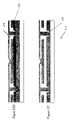
- FIGS. 6A-6Cillustrate three different embodiments of the moving mirror structure.
- FIG. 6Ais a cross section of the embodiment of FIG. 1 , where a strip of metal material 14 is deposited on orthogonally extending supports 18 .
- the moveable reflective material 14is attached to supports at the corners only, on tethers 32 .
- the moveable reflective material 14is suspended from a deformable layer 34 .
- This embodimenthas benefits because the structural design and materials used for the reflective material 14 can be optimized with respect to the optical properties, and the structural design and materials used for the deformable layer 34 can be optimized with respect to desired mechanical properties.
- FIG. 7is a cross-sectional illustration of an embodiment of an interferometric modulator element 112 , which is similar in structure to the modulator element of FIG. 6C .
- the modulator element 112includes a fixed mirror layer within an optical stack 116 formed on a transparent substrate 120 .
- the optical stack 116may comprise two or more distinct layers.
- the optical stack 116comprises an indium tin oxide (ITO) layer underneath a layer of chrome.
- the optical stack 116may comprise an oxide layer located over the chrome layer.
- the optical stack 116is alternately referred to herein as the electrode layer.
- posts 118extend upward from the substrate 120 and support a flexible layer 134 , alternately referred to herein as a deformable layer or a mechanical layer.
- the flexible layer 134is electrically and physically connected to a movable mirror layer 114 via a conductive member 124 .
- An interferometric cavity 119is thus formed between the movable mirror 114 and the fixed mirror within the optical stack 116 .
- the application of a voltage to both the movable mirror 114 and the fixed mirrorwill result in an electrostatic force between layers 114 and 116 causing the flexible layer 134 to deflect, so as to permit the movable mirror 114 to move closer to the optical stack 116 .
- the movable mirror 114can move closer or further from the optical stack 116 , depending on the change in voltage. It is desirable that the posts 118 that support the flexible layer 134 be sufficiently stiff that the posts 118 not bend or deflect when the flexible layer 134 deflects.
- support postssuch as post 118 of FIG. 7 may not be located directly on substrate 120 .
- the support posts 118may instead be located on top of one or more of the layers which form the optical stack 116 , or on top of a masking layer.
- the existence of layers underlying the support postswill depend in part on the particular methods and materials used to create the interferometric modulator.
- support postencompasses not only the variety of post structures depicted or described with respect to the various embodiments disclosed in the application, but also encompasses any structure suitable for providing support for the flexible layer 134 , or similar components of an interferometric modulator element.
- these structuresmay comprise wall-like structures which are substantially longer in one dimension than they are wide in another.
- two intersecting wall structuresmay serve as a single support post, such that if the structures were to be viewed from above, they would form a cross.
- Such alternate structureswhich may provide necessary spacing between components supported by such structures, may advantageously also increase the functional area of the display.
- the term support postis used herein to refer to any of these support-providing structures.
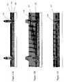
- FIGS. 8A-8Idepict certain steps of one embodiment of a method of making one embodiment of an interferometric modulator element 112 , such as depicted in FIG. 7 .
- Each of FIGS. 8A-8Iis a side cross section view of the element 112 illustrating changes as additional layers are deposited, patterned, and etched in forming the interferometric modulator element 112 .
- the substrate 120 of FIG. 7onto which the element 112 is formed, includes a glass substrate 220 .
- Each of the layers described hereinmay comprise any suitable material known in the art.
- an indium tin oxide (ITO) layer 240and a chrome layer 242 can be deposited onto the glass substrate 220 .
- ITOindium tin oxide
- chrome layer 242can be deposited onto the glass substrate 220 .
- addressing electrodesfor individual modulator elements.
- postswill be formed in the apertures 244 between the electrodes.
- layers of oxide 250 , sacrificial material 252 , and mirror metal 254are deposited over the layer 242 .
- a mask layer 256can be deposited, patterned, and etched to define a post region 258 in the mask layer 256 .
- layers 254 and 252are etched using the mask layer 256 of FIG. 8C to form a hole or opening 260 extending through the layers 254 and 252 down to the oxide layer 250 , after which the mask layer 256 is removed. While the profile of the opening 260 is depicted as v-shaped in the illustrated embodiment, it is to be recognized that the shape of the opening 260 may vary in other embodiments based on details of the photomasks used or on other details of the photolithography and etching processes used in an embodiment.
- a second sacrificial layer 262is deposited onto exposed portions of the layers.
- the sacrificial layers 252 and 262include molybdenum. As discussed above, the process in other embodiments may use any suitable material known in the art to accomplish the steps set forth above.
- a resist layer 272is deposited on the exposed portions of the layers, patterned, and etched to define an aperture 274 in the resist layer 272 .
- the aperture 274corresponds to the location of the conductive member 108 that physically and electrically couples the movable mirror 114 to the deflectable membrane 134 of the interferometric modulator element 112 (See FIG. 7 ).
- the sacrificial layer 262is etched to define an opening corresponding to the conductive member 124 .
- the resist layeris then removed, and a mechanical layer 282 is deposited on the exposed portions of the layers to form the conductive member 124 and the flexible layer 134 of FIG. 7 .
- a resist layer 292is deposited on the mechanical layer 282 and masked to define other structures (not shown) of the mechanical layer.
- the sacrificial layers 252 and 262are removed to define the optical cavity of the interferometric modulator element 112 and to separate the movable mirror 114 from the layers below it and, except for conductive member 124 , from the layers above it as well.
- a xenon diflouride based processis used to remove the sacrificial layers.
- the post 118 in this embodimentis formed above another layer of material, rather than directly on the substrate as depicted in FIG. 7 .
- the post 118is formed over a portion of the oxide layer 250 , rather than directly on the substrate 220 .
- the post 118is thus formed by the mechanical layer 282 of FIG. 8H .
- forming the post opening 260 (as shown in FIG. 8D ), as well as forming the mechanical layer 282 into the post opening(as shown in FIG. 8G ), requires precise process control that can limit the types of fabrication facility and fabrication equipment that can be used to fabricate the interferometric modulator element 112 .
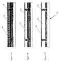
- FIGS. 9A-9Eare cross-sectional views of certain steps of a method of making an alternate embodiment of an interferometric modulator in which a reflective surface is located on the underside of the flexible layer.
- a layer 240 of ITOis deposited on a substrate 220
- a layer 242 of chromeis deposited above the ITO layer 240 .
- Layers 240 and 242are then subsequently patterned and etched to define addressing electrodes for individual modulator elements.
- postswill be formed in the apertures 244 between the electrodes.
- layers 240 and 242are etched so as to form addressing electrodes but leave material at the post locations, such that the posts will overlie this residual material.
- FIG. 9Bit can be seen that a layer 250 of oxide is deposited on top of the chrome layer 242 , and a layer of sacrificial material 252 is deposited above the oxide layer 250 .
- FIG. 9Cit can be seen that a mask layer 356 has been deposited and patterned to form apertures 358 .
- sacrificial layer 252is then etched, using the mask layer 356 as a guide, to form a hole or opening 360 in the sacrificial layer 252 .
- the mask layer 356is removed.
- a mechanical layer 382is then deposited over the sacrificial layer, and along the edges of hole 360 , forming both the deformable layer and the support post structure.
- this mechanical layer 382may be made of a reflective material, such that the layer 382 itself will serve as the movable reflective layer.
- a reflective layer(not shown) may be deposited on the sacrificial layer 252 prior to the deposition of mechanical layer 382 , such that mechanical layer 382 is deposited on top of the reflective layer.
- the mechanical layer 382may then be patterned and etched to form various features (not shown).
- a release etchis then performed to remove the layer 252 of sacrificial material, forming an interferometric cavity 319 , as seen in FIG. 9E .
- An interferometric modulator 312is thus formed in which the underside of the deformable layer 382 serves as the movable reflective surface.
- FIGS. 10A-10Gare cross-sectional views illustrating certain steps of another embodiment of a method of making one embodiment of the interferometric modulator element 112 , such as depicted in FIG. 7 .
- the methodincludes the steps depicted in FIGS. 8A-8E .
- a resist layer 272is deposited on the sacrificial layer 262 and patterned and etched to define apertures 274 and the post openings 260 .
- the apertures 274define the location of the conductive member 124
- the post openings 260define the location of the posts 118 .
- the sacrificial layers 252 and 262are etched using the resist layer 272 as a mask to define an opening 276 for the conductive member 124 and openings 260 for the support post 118 .
- a planararization layer 294is deposited on exposed portions of the layers.
- the planarization layer 294can be formed of organic or polymer materials, or any other suitable photo-patternable material such as are known in the art.
- the planarization layer 294is formed of a photoresist material.
- the planarization layer 294can be formed of spin-on materials, such as spin-on-glass.
- the planarization layer 294is patterned and etched in the form of the post 118 .
- the planarization layer 294 of FIG. 10Dis hardened to increase its rigidity, as more fully explained below.
- the hardened planarization materialthus has increased strength and other improved physical properties as compared to the resist material from which it was originally formed. These improved properties enable the post 118 formed from the hardened material to provide improved support for a flexible layer, such as flexible layer 134 of FIG. 7 .
- the planarization materialin which the planarization material is a photoresist material, the planarization material can be hardened using exposure to high temperatures to heavily cross link, and harden, the photoresist material.
- the mechanical layer 282is desirably deposited over the posts 118 and the sacrificial layer 262 .
- a resist layer 292is deposited and masked to define other structures (not shown) of the mechanical layer 282 .
- the sacrificial layers 252 and 262are removed to define the optical cavity of the interferometric modulator element 112 and to separate the movable mirror 114 from the mechanical layer 134 located above the mirror and the optical stack 116 located below the mirror.
- the planarization materialforms the post 118 . While the planarization material will generally have sufficient hardness to function as a support post over the lifetime of an interferometric display, some slight shift in the color reflected by a particular modulator may occur over time, because the planarization material may never become fully hardened.
- support posts made from planarization materialsmay not be desirable.
- the hardening processtypically undesirably exposes the other layers, e.g., the ITO layer, to high temperatures.
- the modulator elements structureis designed to support the flexible layer 134 in as close to a single plane as is possible.
- the position of the flexible layer 134depends upon residual tensile stresses within the flexible layer, which pull the flexible layer toward a substantially flat position.
- the existence and magnitude of these residual tensile forcesmay be controlled, and depend on factors such as the materials and the parameters of the deposition process, such as the temperature at which the material is deposited and the rate of deposition.
- the effect of these residual tensile forcesis illustrated in in FIG. 10G , wherein the unattached portion of the flexible layer 10 G is substantially flat.
- the resulting flexible layer 134 provided by the process of FIGS. 10A-10Gdoes not lie in a single plane. Rather, the shape of the mechanical layer 282 is affected by the curved upper surface of the posts 118 . In addition, it can be seen that the thickness of the support post 118 underlying the mechanical layer 134 becomes very narrow along the lip 119 of the support post 118 .
- the post 118must exert a restraining force on the flexible layer 134 . Due to the thinness of the support post 118 in the region underlying the flexible layer 134 at the tip 119 of the support post, there is the potential for mechanical failure at the tip 119 .
- This failurecan take the form of partial delamination between the layer 134 and the upper surface of the support post 118 , which may permit the layer 134 to move further away from the fixed mirror within the optical stack 116 , thereby affecting the interferometric properties of the cavity.
- an increased range of movementcould be the result of one or more fractures within the tip 119 of the support post 118 , which would allow the flexible layer 134 to move further upward. If such a mechanical failure occurs, this slight mechanical failure may not occur until a point in time well into the useful lifetime of the interferometric modulator element, and may not result in an easily perceivable shift in the reflected wavelength of the modulator element.
- a flexible layer 134which is slightly curved is suitable. However, this same curvature increases the fragility of the post lips, so over long periods of time, a partially curved mechanical layer may be undesirable.
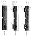
- FIGS. 11A-11Killustrate certain steps of one embodiment of a method of making one embodiment of an interferometric modulator element 112 , such as depicted in FIG. 7 , including steps for forming a post prestructure on the substrate 120 .
- the substrate 120 of FIG. 7includes the glass substrate 220 of FIG. 11A .
- FIG. 11Adepicts an early step in a method of forming an interferometric modulator element 112 wherein a spin on glass (SOG) layer 402 is deposited on a glass substrate 220 and a resist layer 404 is deposited on the SOG layer 402 .
- the layer 402may be formed using other deposition techniques such as by performing physical vapor deposition (PVD), chemical vapor deposition (CVD), plasma chemical vapor deposition (PVCD), or any other suitable process known in the art.
- a masking layermay be deposited on substrate 220 , patterned, and etched prior to the deposition of the layer 402 , which will form posts 118 .
- this masking layeris patterned and etched such that once the interferometric modulator 112 is formed, the masking layer exists only under the support posts 118 .
- the masking layerprevents light from entering the interferometric modulating element in a non-functional area. Subsequent undesired reflections of such stray light can negatively impact the image quality of an interferometric modulator-based display.
- preformed support postssuch as posts 118 of FIG. 11B may be formed of different materials, or in different positions, than the spin-on glass posts of FIG. 11B .
- preformed posts comprising silicon oxide, another oxide material, or metalmay be formed by depositing a layer of oxide via physical vapor deposition (PVD) on the transparent substrate, and then patterning and etching the layer of oxide to form support posts.
- PVDphysical vapor deposition
- support postsparticularly those formed of a material which does not require annealing at temperatures as high as spin-on glass, can be formed after certain other layers have been deposited.
- support posts made of oxide, metal, planarization material, or any other suitable materialare formed after the ITO and chrome layers are deposited on the substrate.
- the placement of support posts above the electrode layer, particularly those support posts made from reflective materialmay advantageously reduce or eliminate the need for a masking layer to hide the reflective lower surface of the post from the viewer, as discussed above.
- the resist layer 404is patterned and developed to yield a mask that allows an etch process to form the post structures 118 from SOG layer 402 of FIG. 11A .
- the post structures 118include at least two posts. Remaining portions of the resist layer form post masks 404 on top of the post structures.
- the mask layer 404can be a lift-off resist, such as a lift-off resist material made by MicroChem Corp, of Newton, Mass.
- the SOG layer 402thus forms a post prestructure on the substrate 220 .
- the ITO layer 240 and chrome layer 242are deposited on the glass substrate 220 , then patterned and etched to form portions of the optical stack 116 of FIG. 7 .
- the rigid glass layer 402 of FIG. 10Ais applied before the ITO 240 and chrome layer 242 , allowing a rigid post 118 to be formed without needing to expose any other layers to high temperature processes that would typically tend to damage materials such as are in the ITO layer 240 .
- the oxide layer 250 , sacrificial layer 252 , and mirror metal layer 254are deposited onto exposed portions of the layers. Note that these layers can also be deposited onto the post mask 404 .
- subsequent layerssuch as the oxide layer 250 are typically shadowed by the post 118 .
- This shadowingcauses the oxides 250 to taper off to the post. This taper is not so severe as to cause the oxide to fail to cover the underlying ITO 240 and chrome 242 layers and not so extensive as to extend beyond the minimum feature size gap that would normally exist between the post and the mirror. Thus the shadowing effect does not impact the optical performance or percent active area of the modulator.
- the mirror metal layer 254is patterned and etched away from the posts 118 to define gaps 460 between the post 118 and the mirror layer 254 .
- another sacrificial layer 462is deposited on exposed portions of the layers.
- the sacrificial layers 252 and 462are molybdenum.
- the post mask 404and the residual layers that have been deposited on top of it, are removed using techniques such as those well known in the art.
- the lift-off resist removal techniqueis used.
- a planarization matieralwhich in this case is a resist layer 472 , is deposited on exposed portions of the layers, patterned, and etched to define a cavity 474 .
- the sacrificial layer 462is etched to further define the cavity 474 .
- the cavity 474defines the form of the conductive connector 124 that extends between the flexible layer 134 and the mirror 114 (see FIG. 7 ).
- etch-back planarizationis performed to etch the resist layer 472 back to the sacrificial layer 462 so that the top of the post 118 , the remaining resist 472 and the sacrificial layer 462 define a substantially planar surface.
- a mechanical layer 492is deposited on this substantially planar surface. The mechanical layer 492 also fills the cavity 474 to form the conductive connector 124 . At this point, pattern and etch steps are performed on the mechanical layer 492 .
- the remaining resist layer 472is removed, for example, by using an asher, e.g., a barrel etcher or a plasma etcher, to oxidize the resist layer 472 to form a cavity 476 .
- an ashere.g., a barrel etcher or a plasma etcher
- the sacrificial layersare removed.
- xenon difluorideis used to remove the sacrificial layers 252 and 462 .
- the movable mirror 114 and the deflectable membrane 134are thus separated from the fixed members of the element 112 .
- embodimentsmay include other processing steps.
- other features in the mechanical layer 492can be formed during the pattern and etch of this layer.
- the post materialmay be deposited as a layer 402 which is then etched to form support posts 118 , as seen in FIGS. 11A and 11B , greater control over the shape of the upper surface of the posts 118 is available than in the case where the posts are formed after other material has been deposited on the substrate.
- flexible layerswhich are substantially flat along the upper surface of the support posts can be formed, and the post can be made of more robust material than can be deposited later in the process.
- etch-back planarization processto provide a substantially flat surface (as seen in FIG. 11H ) prior to forming the mechanical layer also permits, in conjunction with the flat support posts discussed above, the formation on that surface of a substantially flat mechanical layer.
- the mechanical layerneed not be completely flat, particularly due to the deposition of the mechanical layer in the cavity 474 .
- the substantially flat flexible layer resulting from the deposition of this mechanical layeris far less likely to undergo mechanical failure of the type discussed above, than is the embodiment of FIG. 10G .
- the flexible layer 134is formed in, and tends to dwell in, a state in which the entire layer 134 is substantially flat, the residual tensile forces will not contribute to mechanical failure which permits movement of the flexible layer 134 father upward than is already permitted. Specifically, because the residual tensile forces are pulling in a direction parallel to the upper surface of the support posts 118 when the flexible layer 134 is in the unactuated state, there will be significantly less risk of delamination between the flexible layer 134 and the support post 118 than if the surface was oriented in a direction not parallel to the tensile force. Similarly, because the support posts 118 of FIG. 11K do not have a thin edge portion such as the lip 119 of FIG.
- FIGS. 12A-12Eare cross-sectional views illustrating certain steps of another embodiment of a method of making one embodiment of the interferometric modulator element 112 , such as depicted in FIG. 7 , including steps for forming a post prestructure on the substrate 120 .
- This embodimentincludes the steps depicted in FIGS. 11A-11E .
- FIG. 12Arather than depositing the second sacrificial layer 462 on the mirror metal layer 254 and exposed portions of other layers, as is done in the steps described with respect to FIG.
- the residual layersare stripped from the tops of the posts 118 and planarization material, which in this embodiment is a resist layer 502 , is deposited in place of the second sacficifial layer 462 of FIG. 11F .
- the resist layer 502is patterned and etched to define the region 474 into which the conductor 124 can be formed.
- etch back planarizationis performed on the resist layer 502 so that the resist layer and the post 118 define a substantially planar surface.
- the mechanical layer 492is deposited as in the embodiment depicted in FIG. 11I .
- the mechanical layer 492is subsequently patterned and etched.
- an asheris used to oxidize away the resist layer 502 (shown in FIG. 12C ) to define the open region 476 .
- the region 476is larger than in the embodiment depicted in FIG. 11I because the region 476 in this embodiment also includes the volume that was occupied by the sacrificial layer 462 in FIG. 11I .
- the sacrificial layer 252 of FIG. 11Dis removed to define the interferometric modulator element 112 .
- the embodiment depicted in FIGS. 12A-12Edesirably uses the photoresist layer 502 , which is also used to pattern the aperture 474 for the conductor 124 , as the second sacrificial layer 462 so as to reduce the total number of process steps as compared to the embodiment depicted in FIGS. 10A-10K .
- planarization materialis used to provide the upper sacrificial layer, etch-back planarization can be performed, permitting the formation of a modulator element which, as discussed with respect to FIG. 11K , is less susceptible to changes in its interferometric properties over time.
- preformed posts 118can be used to support a combination mechanical/reflective layer, such as layer 382 of FIG. 9G , creating an interferometric modulator similar to the modulator of FIG. 6A .
- a method of fabricating such an embodimentincludes steps of FIGS. 11A-11C . Following these steps, as illustrated in FIG. 13A , an oxide layer 250 is deposited over the chrome layer 242 , and a layer of sacrificial material 252 is deposited over the oxide layer 250 .
- FIG. 13Bit can be seen that the remnants of previously deposited layers overlying the support posts 118 are stripped from the top of the posts, and a resist layer 512 is deposited over the sacrificial layer 252 .
- FIG. 13Cetch-back planarization is performed on the resist layer 512 such that the remaining resist layer 512 and support posts 118 define a substantially planar surface.
- a mechanical layer 492is then deposited over the substantially planar surface provided by the resist layer 512 and the support posts 118 .
- this mechanical layer 492may be made of a reflective material, such that the layer itself will serve as the movable reflective layer.
- a reflective layer(not shown) may be deposited on the resist layer 512 prior to the deposition of mechanical layer 492 , such that mechanical layer 492 is deposited on top of the reflective layer.
- the mechanical layer 492is then patterned and etched to form various features (not shown).
- an asheris used to oxidize away the resist layer 512 (shown in FIG. 13D ) to define an open region 476 .
- a release etchis then performed to remove the layer 252 of sacrificial material, forming an interferometric cavity 519 , as seen in FIG. 13F .
- An interferometric modulator 512 in which the underside of the deformable layer 492 serves as the movable reflective surfaceis thus formed.
- any residual tensile forces within the deformable layer 492will not tend to cause mechanical failures of the type discussed above, but will instead bias the deformable layer 492 to return to the position depicted in FIG. 13F .
- a method for forming cap structures above postsincludes the steps of FIG. 11A-11I , wherein preformed support posts comprising a material such as spin-on glass are fabricated, a planarization layer is used to provide a substantially flat surface, and a mechanical layer is deposited over the substantially flat surface and etched to form various features (not depicted), as discussed above.
- a layer of insulating material 740is deposited over the mechanical layer 492 .
- a layer of rigid material 750is then deposited over the insulating layer 740 .
- the layer of rigid materialmay not be necessary, if the layer of insulating material 740 is sufficiently thick and/or rigid.
- the layer of insulating material 740may comprise, in one embodiment, an oxide such as silicon oxide, but any suitable material which can serve as an electrical insulator may be used.
- the layer of rigid material 750may be any suitable material, and the use of an insulating layer 740 in contact with the patterned mechanical layer 492 enables the use of electrically conductive material in the rigid layer 750 , as the rigid layer is electrically isolated from the mechanical layer.
- the rigid layer 750comprises the same material used in the mechanical layer 492 .
- both the mechanical layer 492 and the rigid layer 750comprise nickel.
- one or both of the layers 492 and 750may comprise aluminum.
- a wide range of materialsmay be suitable for use in the rigid layer 750 , as depositing a sufficiently thick layer of these materials may provide the necessary rigidity.
- FIG. 14Bit can be seen that the rigid layer 750 has been etched, using the insulator layer 740 as an etch stop.
- the insulator layer 740has itself then been etched, using the mechanical layer 492 and the underlying sacrificial layer 462 and the remnants of the resist layer 472 as etch stops.
- cap structures 760 having a rigid layer 750 overlying an insulating layer 740are formed above posts 118 .
- the resist layer 472is removed, such as by using an asher, as discussed previously, leaving cavities 474 .
- a release etchis performed to remove the sacrificial layers 462 and 452 , separating the mirror layer 114 from the flexible layer 134 above the mirror and the optical stack 116 below the mirror, thereby forming a modulator element 712 . If the mechanical layer 492 (see FIG. 14C ) was previously etched so as to totally remove the mechanical layer from above the posts 118 , a mechanical layer 492 (see FIG. 14C ) forms a flexible layer 134 wherein the flexible layer is suspended from the insulated underside of the caps 760 .
- the caps 760extend at least partially over the mirrors 114 , the surface area required for electrical isolation does not negatively impact the amount of functional area in the modulator element 712 .
- the caps 760may be formed solely of insulating material 740 , if the insulating material has sufficient thickness or rigidity to support the flexible layer 134 .
- the preformed support postsmay comprise a column of conductive material such that the top of the post 118 may be placed in electrical communication with an element located below the post.
- the insulating layer 740may be etched over the support post so as to expose the conductive material within the post 118 without exposing the patterned mechanical layer 492 .
- the layer of rigid material 750is deposited over the insulating layer 740 , the cavity in the insulating layer is filled, and provided the rigid material 750 is electrically conductive, an electrical connection can be made between the top of the resulting cap 760 and an element underlying the post 118 .
- Overlying support materialmay be formed above the other types of support posts discussed in this application.
- a method of providing an overlying cap structureincludes the steps depicted in FIGS. 10A-10F .
- a layer of insulating material 740is deposited over the patterned mechanical layer 282 , and a layer of rigid support material 750 is then deposited over the insulating layer 740 , as can be seen in FIG. 15A .
- cap structures 760have been created by etching the rigid support layer 750 , using the insulating layer 740 as an etch stop.
- the insulating layer 740has then been etched, using the underlying mechanical layer 282 and sacrificial layer 262 as etch stops.
- an interferometric modulator element 712is formed, by etching the sacrificial material 252 and 262 to release the mirror 114 , as discussed above.
- the interferometric modulator element 712comprises posts 188 made from planarization material, and an overlying cap 760 , which provides additional support for the flexible layer 134 .
- the mechanical layer 282may be etched so as to completely remove the mechanical layer overlying the curved upper surface of the posts 188 .
- the caps 760can then extend sufficiently beyond the edges of the post 188 to support the flexible layer 134 .
- FIGS. 8A-8HAnother method of providing additional support for support posts, such as the support posts 118 of FIG. 8I , includes the steps of FIGS. 8A-8H .
- an insulating layer 740 and a support layer 750are deposited above the patterned mechanical layer 282 , as seen in FIG. 16A .
- the rigid support layer 750is first etched, followed by the insulator layer 740 , forming a cap structure 760 of additional support material.
- an interferometric modulator 712is formed by performing a release etch, removing the sacrificial layers 262 and 252 , releasing the mirror 114 , as discussed above.
- FIG. 17FAnother method of forming cap structures includes forming an interferometric modulator comprising freestanding support posts 652 (see FIG. 17F ). This method includes the process of FIGS. 8A-8E . Following that process, in FIG. 17A , a resist layer 640 is deposited over the sacrificial layer 262 . However, unlike the resist mask 272 of FIG. 8F , the resist mask 640 of FIG. 17A need not have an aperture 274 for etching. Rather, the resist mask 640 need only provide apertures within the post holes 260 , for etching the portion of sacrificial layer 262 exposed by the resist mask 640 .
- FIG. 17Bit can be seen that the resist mask has been used to etch the sacrificial layer 262 to expose the oxide layer 250 underneath the post hole 260 of FIG. 17A .
- a layer of support post material 650is then deposited.
- the support post materialis non-planarizing, and thus the deposited layer conforms to the shape of the underlying layers, leaving part of the post hole 260 unfilled, rather than filling the entirety of the post hole.
- the layer of support post material 650may comprise material suitable for use as a mechanical layer, it will be understood that the selection of support post material need not be so limited. Rather, the support post material 650 may advantageously be a material which has significant rigidity, rather than the flexibility desirable in mechanical layer material. Additionally, the support post material 650 is desirably selectively etchable relative to the sacrificial layer 262 .
- support post material 650has been patterned and etched such that certain support post material beyond the vicinity of the post holes 260 (see FIG. 17A ) has been removed, leaving support posts 652 .
- these support postsare roughly symmetrical about a central axis, and are thus substantially conical in shape in the center, having a wide, substantially flat outer edge area.
- the support postsmay be wider in one direction than in another, and are thus substantially wedge-shaped.
- a layer of insulating material 840is deposited over the support posts 652 and the exposed underlying sacrificial layer 262 .
- the insulating material 840is then patterned and etched so as to remove certain insulating material 840 overlying the sacrificial material 262 , leaving insulating material only in the area around the support posts 652 .
- An aperture 874is then etched in the sacrificial layer, exposing the underlying mirror layer 254 .
- FIG. 17Eit can be seen that a mechanical layer 860 is then deposited, such that it overlies the insulating material 840 and fills the aperture 874 .
- the mechanical layer 860is then patterned and etched to form features (not shown).
- FIG. 17Fit can be seen that a release etch has been performed to remove the sacrificial material 262 and 252 , separating the mirror 114 from the surrounding material, as discussed above.
- An interferometric modulator element 812is thus formed, having cap structures formed from insulating material 840 , which are located above posts 652 and provide support for the flexible layer 134 . In the depicted embodiment, no additional rigid support layer may be necessary, as the wide underlying support post 652 may provide sufficient rigidity.
- the order of layers and the materials forming these layers in the above embodimentsare merely exemplary.
- no sacrificial layerneed be deposited.
- the planarization layercan serve as the entire sacrificial material, which will then be removed to form the cavity between the deformable upper layer and the optical stack.
- other layersnot shown, may be deposited and processed to form portions of the interferometric modulator element 112 or to form other structures on the substrate.
- these layersmay be formed using alternative deposition materials, may be deposited in different order, or composed of different materials, as would be known to one of skill in the art, or as also discussed in more detail in the patents and applications discussed above.
- cap structures discussed abovemay be utilized in embodiments in which the flexible layer serves as the movable reflective layer.
- the embodiment depicted in FIG. 13Fmay be modified to include cap structures at the top of the support posts, from which the flexible reflective layer is suspended.
- Other embodiments having a combination movable/reflective layermay be similarly modified to provide additional support, improved mechanical characteristics, and increased functional area within the display.
Landscapes
- Physics & Mathematics (AREA)
- Engineering & Computer Science (AREA)
- Manufacturing & Machinery (AREA)
- Spectroscopy & Molecular Physics (AREA)
- General Physics & Mathematics (AREA)
- Optics & Photonics (AREA)
- Microelectronics & Electronic Packaging (AREA)
- Mechanical Light Control Or Optical Switches (AREA)
- Micromachines (AREA)
Abstract
Description
This application claims priority under 35 U.S.C. § 119(e) to U.S. Provisional Application Ser. No. 60/613,411, filed on Sep. 27, 2004, which is hereby incorporated by reference in its entirety.
1. Field of the Invention
The field of the invention relates to microelectromechanical systems (MEMS).
2. Description of the Related Technology
Microelectromechanical systems (MEMS) include micro mechanical elements, actuators, and electronics. Micromechanical elements may be created using deposition, etching, and or other micromachining processes that etch away parts of substrates and/or deposited material layers or that add layers to form electrical and electromechanical devices. One type of MEMS device is called an interferometric modulator. As used herein, the term interferometric modulator or interferometric light modulator refers to a device that selectively absorbs and/or reflects light using the principles of optical interference. In certain embodiments, an interferometric modulator may comprise a pair of conductive plates, one or both of which may be transparent and/or reflective in whole or part and capable of relative motion upon application of an appropriate electrical signal. In a particular embodiment, one plate may comprise a stationary layer deposited on a substrate and the other plate may comprise a metallic membrane separated from the stationary layer by an air gap. As described herein in more detail, the position of one plate in relation to another can change the optical interference of light incident on the interferometric modulator. Such devices have a wide range of applications, and it would be beneficial in the art to utilize and/or modify the characteristics of these types of devices so that their features can be exploited in improving existing products and creating new products that have not yet been developed.
In one embodiment, a method of forming an interferometric display element is provided, including providing a substrate, depositing a layer of support post material over the substrate, patterning the layer of support post material to form at least two support posts, forming an electrode layer over the substrate, where the forming of the electrode layer is done after the forming of the at least two support posts, forming at least a first sacrificial layer over the electrode layer, and forming a mechanical layer over the sacrificial layer, where the mechanical layer covers a portion of each of the at least two support posts.
In another embodiment, an apparatus including a plurality of interferometric modulator elements is provided, where the interferometric modulator elements include an electrode layer located over the substrate, at least two support posts located on the substrate, and a mechanical layer located over the electrode layer, where the mechanical layer is supported by at least two support posts.
In another embodiment, a method of forming an interferometric display element is provided, including providing a substrate, forming an electrode layer over the substrate, forming at least two support posts over the substrate, wherein the forming of the at least two support posts is done after the forming of the electrode layer, forming at least a first sacrificial layer over the electrode layer, and forming a mechanical layer over the sacrificial layer, where the mechanical layer covers a portion of each of the at least two support posts.
In another embodiment, a display including a plurality of interferometric display elements is provided, where said interferometric display elements include a substrate, an electrode layer located over the substrate, at least two support posts located on the electrode layer, where the posts include planarization material, and a mechanical layer located over the electrode layer, said mechanical layer being supported by the at least two support posts.
In another embodiment, a display containing a plurality of interferometric modulators is provided, where the interferometric modulators are formed by a method including providing a substrate, depositing a layer of support post material over the substrate, patterning the layer of support post material to form at least two support posts, forming an electrode layer over the substrate, where the forming of the electrode layer is done after the forming of the at least two support posts, forming at least a first sacrificial layer over the electrode layer, and forming a mechanical layer over the sacrificial layer, where the mechanical layer covers a portion of each of the at least two support posts.
In another embodiment, a method of making an interferometric display element is provided, including providing a substrate, forming support posts over the substrate, forming an electrode layer over the substrate, depositing a sacrificial layer over the electrode layer forming a substantially planar surface over the sacrificial layer, forming a mechanical layer over the substantially planar surface, forming an insulator layer over at least part of the mechanical layer; and forming a substantially rigid support layer over the insulation layer.
In another embodiment, an apparatus is provided, including a substrate, an electrode layer located over the substrate, a plurality of support posts located over the substrate, a rigid cap member located over each of at least some of the plurality of support posts, where the rigid cap member includes an insulator layer, and a mechanical layer located over the partially reflective electrode layer, where said mechanical layer is attached to the insulator layers of at least two rigid cap members.
In another embodiment, a method of making a display element is provided, including depositing an electrode layer on a substrate, patterning the electrode layer, depositing a layer of sacrificial material over the electrode layer, patterning the layer of sacrificial material to form apertures, forming support posts in the apertures, forming a flexible layer over the layer of sacrificial material, depositing an insulator layer over the flexible layer, depositing a rigid support layer over the insulator layer; and removing the sacrificial material; thereby permitting movement of the flexible layer relative to the substrate.
In yet another embodiment, a method of making a display element is provided, including depositing an electrode layer on a substrate, patterning the electrode layer, depositing a layer of sacrificial material over the electrode layer, patterning the layer of sacrificial material to form apertures, depositing a layer of non-planarizing support post material on the sacrificial material, and patterning the non-planarizing support post material so as to remove support post material located away from the apertures, forming support posts, forming a flexible layer over the support posts, and removing the sacrificial material; permitting movement of the flexible layer relative to the substrate.
In yet another embodiment, a display containing a plurality of interferometric modulators is provided, where the interferometric modulators are formed by a method including providing a substrate, forming support posts over the substrate forming an electrode layer over the substrate, depositing a sacrificial layer over the electrode layer, forming a substantially planar surface over the sacrificial layer, forming a mechanical layer over the substantially planar surface, forming an insulator layer over at least part of the mechanical layer, and forming a substantially rigid support layer over the insulation layer.
An embodiment of the invention, as discussed in greater detail below, is an interferometric modulator element which includes an upper mechanical layer supported by at least two support posts. In one embodiment, these support posts are formed on a substrate before other layers are deposited on the substrate. Such a method advantageously permits the use of spin-on glass support posts, and other materials which must be annealed at a temperature high enough to damage other components of the interferometric modulator if those components were deposited before the annealing of the post.
In other embodiments, support posts made from materials with lower annealing temperatures may be formed after the deposition of certain layers of materials having higher annealing temperatures, permitting the creation of support posts over these layers. Such an embodiment advantageously minimizes or eliminates the need for a masking layer between the posts and the viewer, as the layers on which the support posts rest may prevent the support posts from reflecting light back to the viewer.
Another embodiment of the invention, as discussed in greater detail below, is a method of making an interferometric modulator element which includes a rigid cap portion atop at least two support posts. The method may also include providing a substantially planar surface on which the mechanical layer can be formed. The use of a cap portion advantageously provides additional rigidity to the support posts. In addition, the use of a rigid cap portion advantageously permits the use of thin support posts, providing the necessary surface area to support and electrically isolate adjacent mechanical layers. The use of a substantially flat mechanical layer advantageously prevents problems such as delamination between the support post and the mechanical layer, or damage to the edge of the support post, which might otherwise occur over time as a result of the residual tensile stresses in a non-flat mechanical layer. Thus, this invention provides a modulator having improved greater color accuracy over a longer period of time.
The following detailed description is directed to certain specific embodiments of the invention. However, the invention can be embodied in a multitude of different ways. In this description, reference is made to the drawings wherein like parts are designated with like numerals throughout. As will be apparent from the following description, the embodiments may be implemented in any device that is configured to display an image, whether in motion (e.g., video) or stationary (e.g., still image), and whether textual or pictorial. More particularly, it is contemplated that the embodiments may be implemented in or associated with a variety of electronic devices such as, but not limited to, mobile telephones, wireless devices, personal data assistants (PDAs), hand-held or portable computers, GPS receivers/navigators, cameras, MP3 players, camcorders, game consoles, wrist watches, clocks, calculators, television monitors, flat panel displays, computer monitors, auto displays (e.g., odometer display, etc.), cockpit controls and/or displays, display of camera views (e.g., display of a rear view camera in a vehicle), electronic photographs, electronic billboards or signs, projectors, architectural structures, packaging, and aesthetic structures (e.g., display of images on a piece of jewelry). MEMS devices of similar structure to those described herein can also be used in non-display applications such as in electronic switching devices.
One interferometric modulator display embodiment comprising an interferometric MEMS display element is illustrated inFIG. 1 . In these devices, the pixels are in either a bright or dark state. In the bright (“on” or “open”) state, the display element reflects a large portion of incident visible light to a user. When in the dark (“off” or “closed”) state, the display element reflects little incident visible light to the user. Depending on the embodiment, the light reflectance properties of the “on” and “off” states may be reversed. MEMS pixels can be configured to reflect predominantly at selected colors, allowing for a color display in addition to black and white.
The depicted portion of the pixel array inFIG. 1 includes two adjacentinterferometric modulators interferometric modulator 12aon the left, a movable and highlyreflective layer 14ais illustrated in a relaxed position at a predetermined distance from a fixed partiallyreflective layer 16a.In theinterferometric modulator 12bon the right, the movable highlyreflective layer 14bis illustrated in an actuated position adjacent to the fixed partiallyreflective layer 16b.
The fixed layers16a,16bare electrically conductive, partially transparent and partially reflective, and may be fabricated, for example, by depositing one or more layers each of chromium and indium-tin-oxide onto atransparent substrate 20. The layers are patterned into parallel strips, and may form row electrodes in a display device as described further below. Themovable layers row electrodes posts 18 and an intervening sacrificial material deposited between theposts 18. When the sacrificial material is etched away, the deformable metal layers14a,14bare separated from the fixed metal layers by a definedgap 19. A highly conductive and reflective material such as aluminum may be used for the deformable layers, and these strips may form column electrodes in a display device.
With no applied voltage, thecavity 19 remains between thelayers pixel 12ainFIG. 1 . However, when a potential difference is applied to a selected row and column, the capacitor formed at the intersection of the row and column electrodes at the corresponding pixel becomes charged, and electrostatic forces pull the electrodes together. If the voltage is high enough, the movable layer is deformed and is forced against the fixed layer (a dielectric material which is not illustrated in this Figure may be deposited on the fixed layer to prevent shorting and control the separation distance) as illustrated by thepixel 12bon the right inFIG. 1 . The behavior is the same regardless of the polarity of the applied potential difference. In this way, row/column actuation that can control the reflective vs. non-reflective pixel states is analogous in many ways to that used in conventional LCD and other display technologies.
In one embodiment, theprocessor 21 is also configured to communicate with anarray controller 22. In one embodiment, thearray controller 22 includes arow driver circuit 24 and acolumn driver circuit 26 that provide signals to a display array orpanel 30. The cross section of the array illustrated inFIG. 1 is shown by the lines1-1 inFIG. 2 . For MEMS interferometric modulators, the row/column actuation protocol may take advantage of a hysteresis property of these devices illustrated inFIG. 3 . It may require, for example, a 10 volt potential difference to cause a movable layer to deform from the relaxed state to the actuated state. However, when the voltage is reduced from that value, the movable layer maintains its state as the voltage drops back below 10 volts. In the exemplary embodiment ofFIG. 3 , the movable layer does not relax completely until the voltage drops below 2 volts. There is thus a range of voltage, about 3 to 7 V in the example illustrated inFIG. 3 , where there exists a window of applied voltage within which the device is stable in either the relaxed or actuated state. This is referred to herein as the “hysteresis window” or “stability window.” For a display array having the hysteresis characteristics ofFIG. 3 , the row/column actuation protocol can be designed such that during row strobing, pixels in the strobed row that are to be actuated are exposed to a voltage difference of about 10 volts, and pixels that are to be relaxed are exposed to a voltage difference of close to zero volts. After the strobe, the pixels are exposed to a steady state voltage difference of about 5 volts such that they remain in whatever state the row strobe put them in. After being written, each pixel sees a potential difference within the “stability window” of 3-7 volts in this example. This feature makes the pixel design illustrated inFIG. 1 stable under the same applied voltage conditions in either an actuated or relaxed pre-existing state. Since each pixel of the interferometric modulator, whether in the actuated or relaxed state, is essentially a capacitor formed by the fixed and moving reflective layers, this stable state can be held at a voltage within the hysteresis window with almost no power dissipation. Essentially no current flows into the pixel if the applied potential is fixed.
In typical applications, a display frame may be created by asserting the set of column electrodes in accordance with the desired set of actuated pixels in the first row. A row pulse is then applied to therow 1 electrode, actuating the pixels corresponding to the asserted column lines. The asserted set of column electrodes is then changed to correspond to the desired set of actuated pixels in the second row. A pulse is then applied to therow 2 electrode, actuating the appropriate pixels inrow 2 in accordance with the asserted column electrodes. Therow 1 pixels are unaffected by therow 2 pulse, and remain in the state they were set to during therow 1 pulse. This may be repeated for the entire series of rows in a sequential fashion to produce the frame. Generally, the frames are refreshed and/or updated with new display data by continually repeating this process at some desired number of frames per second. A wide variety of protocols for driving row and column electrodes of pixel arrays to produce display frames are also well known and may be used in conjunction with the present invention.
In theFIG. 5A frame, pixels (1,1), (1,2), (2,2), (3,2) and (3,3) are actuated. To accomplish this, during a “line time” forrow 1,columns column 3 is set to +5 volts. This does not change the state of any pixels, because all the pixels remain in the 3-7 volt stability window.Row 1 is then strobed with a pulse that goes from 0, up to 5 volts, and back to zero. This actuates the (1,1) and (1,2) pixels and relaxes the (1,3) pixel. No other pixels in the array are affected. To setrow 2 as desired,column 2 is set to −5 volts, andcolumns Row 3 is similarly set by settingcolumns column 1 to +5 volts. Therow 3 strobe sets therow 3 pixels as shown inFIG. 5A . After writing the frame, the row potentials are zero, and the column potentials can remain at either +5 or −5 volts, and the display is then stable in the arrangement ofFIG. 5A . It will be appreciated that the same procedure can be employed for arrays of dozens or hundreds of rows and columns. It will also be appreciated that the timing, sequence, and levels of voltages used to perform row and column actuation can be varied widely within the general principles outlined above, and the above example is exemplary only, and any actuation voltage method can be used with the systems and methods described herein.
Thedisplay device 40 includes ahousing 41, adisplay 30, anantenna 43, aspeaker 44, aninput device 48, and amicrophone 46. Thehousing 41 is generally formed from any of a variety of manufacturing processes as are well known to those of skill in the art, including injection molding, and vacuum forming. In addition, thehousing 41 may be made from any of a variety of materials, including but not limited to plastic, metal, glass, rubber, and ceramic, or a combination thereof. In one embodiment thehousing 41 includes removable portions (not shown) that may be interchanged with other removable portions of different color, or containing different logos, pictures, or symbols.
Thedisplay 30 ofexemplary display device 40 may be any of a variety of displays, including a bi-stable display, as described herein. In other embodiments, thedisplay 30 includes a flat-panel display, such as plasma, EL, OLED, STN LCD, or TFT LCD as described above, or a non-flat-panel display, such as a CRT or other tube device, as is well known to those of skill in the art. However, for purposes of describing the present embodiment, thedisplay 30 includes an interferometric modulator display, as described herein.
The components of one embodiment ofexemplary display device 40 are schematically illustrated inFIG. 18B . The illustratedexemplary display device 40 includes ahousing 41 and can include additional components at least partially enclosed therein. For example, in one embodiment, theexemplary display device 40 includes a network interface27 that includes anantenna 43 which is coupled to atransceiver 47. Thetransceiver 47 is connected to aprocessor 21, which is connected toconditioning hardware 52. [Theconditioning hardware 52 may be configured to condition a signal (e.g. filter a signal).] Theconditioning hardware 52 is connected to aspeaker 44 and amicrophone 46. Theprocessor 21 is also connected to aninput device 48 and adriver controller 29. Thedriver controller 29 is coupled to aframe buffer 28, and to anarray driver 22, which in turn is coupled to adisplay array 30. Apower supply 50 provides power to all components as required by the particularexemplary display device 40 design.
The network interface27 includes theantenna 43 and thetransceiver 47 so that theexemplary display device 40 can communicate with one ore more devices over a network. In one embodiment the network interface27 may also have some processing capabilities to relieve requirements of theprocessor 21. Theantenna 43 is any antenna known to those of skill in the art for transmitting and receiving signals. In one embodiment, the antenna transmits and receives RF signals according to the IEEE 802.11 standard, including IEEE 802.11(a), (b), or (g). In another embodiment, the antenna transmits and receives RF signals according to the BLUETOOTH standard. In the case of a cellular telephone, the antenna is designed to receive CDMA, GSM, AMPS or other known signals that are used to communicate within a wireless cell phone network. Thetransceiver 47 pre-processes the signals received from theantenna 43 so that they may be received by and further manipulated by theprocessor 21. Thetransceiver 47 also processes signals received from theprocessor 21 so that they may be transmitted from theexemplary display device 40 via theantenna 43.
In an alternative embodiment, thetransceiver 47 can be replaced by a receiver. In yet another alternative embodiment, network interface27 can be replaced by an image source, which can store or generate image data to be sent to theprocessor 21. For example, the image source can be a digital video disc (DVD) or a hard-disc drive that contains image data, or a software module that generates image data.
In one embodiment, theprocessor 21 includes a microcontroller, CPU, or logic unit to control operation of theexemplary display device 40.Conditioning hardware 52 generally includes amplifiers and filters for transmitting signals to thespeaker 44, and for receiving signals from themicrophone 46.Conditioning hardware 52 may be discrete components within theexemplary display device 40, or may be incorporated within theprocessor 21 or other components.
Thedriver controller 29 takes the raw image data generated by theprocessor 21 either directly from theprocessor 21 or from theframe buffer 28 and reformats the raw image data appropriately for high speed transmission to thearray driver 22. Specifically, thedriver controller 29 reformats the raw image data into a data flow having a raster-like format, such that it has a time order suitable for scanning across thedisplay array 30. Then thedriver controller 29 sends the formatted information to thearray driver 22. Although adriver controller 29, such as a LCD controller, is often associated with thesystem processor 21 as a stand-alone Integrated Circuit (IC), such controllers may be implemented in many ways. They may be embedded in theprocessor 21 as hardware, embedded in theprocessor 21 as software, or fully integrated in hardware with thearray driver 22.
Typically, thearray driver 22 receives the formatted information from thedriver controller 29 and reformats the video data into a parallel set of waveforms that are applied many times per second to the hundreds and sometimes thousands of leads coming from the display's x-y matrix of pixels.
In one embodiment, thedriver controller 29,array driver 22, anddisplay array 30 are appropriate for any of the types of displays described herein. For example, in one embodiment,driver controller 29 is a conventional display controller or a bi-stable display controller (e.g., an interferometric modulator controller). In another embodiment,array driver 22 is a conventional driver or a bi-stable display driver (e.g., an interferometric modulator display). In one embodiment, adriver controller 29 is integrated with thearray driver 22. Such an embodiment is common in highly integrated systems such as cellular phones, watches, and other small area displays. In yet another embodiment,display array 30 is a typical display array or a bi-stable display array (e.g., a display including an array of interferometric modulators).
Theinput device 48 allows a user to control the operation of theexemplary display device 40. In one embodiment,input device 48 includes a keypad, such as a QWERTY keyboard or a telephone keypad, a button, a switch, a touch-sensitive screen, a pressure- or heat-sensitive membrane. In one embodiment, themicrophone 46 is an input device for theexemplary display device 40. When themicrophone 46 is used to input data to the device, voice commands may be provided by a user for controlling operations of theexemplary display device 40.
In some implementations control programmability resides, as described above, in a driver controller which can be located in several places in the electronic display system. In some cases control programmability resides in thearray driver 22. Those of skill in the art will recognize that the above-described optimization may be implemented in any number of hardware and/or software components and in various configurations.
The details of the structure of interferometric modulators that operate in accordance with the principles set forth above may vary widely. For example,FIGS. 6A-6C illustrate three different embodiments of the moving mirror structure.FIG. 6A is a cross section of the embodiment ofFIG. 1 , where a strip ofmetal material 14 is deposited on orthogonally extending supports18. InFIG. 6B , the moveablereflective material 14 is attached to supports at the corners only, ontethers 32. InFIG. 6C , the moveablereflective material 14 is suspended from adeformable layer 34. This embodiment has benefits because the structural design and materials used for thereflective material 14 can be optimized with respect to the optical properties, and the structural design and materials used for thedeformable layer 34 can be optimized with respect to desired mechanical properties. The production of various types of interferometric devices is described in a variety of published documents, including, for example, U.S. Published Application 2004/0051929. A wide variety of known techniques may be used to produce the above described structures involving a series of material deposition, patterning, and etching steps.
As discussed with respect to previous embodiments, the application of a voltage to both themovable mirror 114 and the fixed mirror will result in an electrostatic force betweenlayers flexible layer 134 to deflect, so as to permit themovable mirror 114 to move closer to theoptical stack 116. When the applied voltage is changed, themovable mirror 114 can move closer or further from theoptical stack 116, depending on the change in voltage. It is desirable that theposts 118 that support theflexible layer 134 be sufficiently stiff that theposts 118 not bend or deflect when theflexible layer 134 deflects.
As will be explained in greater detail below, support posts such aspost 118 ofFIG. 7 may not be located directly onsubstrate 120. Although not shown inFIG. 7 , the support posts118 may instead be located on top of one or more of the layers which form theoptical stack 116, or on top of a masking layer. As will be apparent from the following detailed description, the existence of layers underlying the support posts will depend in part on the particular methods and materials used to create the interferometric modulator.
The term “support post” encompasses not only the variety of post structures depicted or described with respect to the various embodiments disclosed in the application, but also encompasses any structure suitable for providing support for theflexible layer 134, or similar components of an interferometric modulator element. For example, in certain embodiments, these structures may comprise wall-like structures which are substantially longer in one dimension than they are wide in another. In a further embodiment, two intersecting wall structures may serve as a single support post, such that if the structures were to be viewed from above, they would form a cross. Such alternate structures, which may provide necessary spacing between components supported by such structures, may advantageously also increase the functional area of the display. For convenience, the term support post is used herein to refer to any of these support-providing structures.
Proceeding toFIG. 8D , layers254 and252 are etched using themask layer 256 ofFIG. 8C to form a hole oropening 260 extending through thelayers oxide layer 250, after which themask layer 256 is removed. While the profile of theopening 260 is depicted as v-shaped in the illustrated embodiment, it is to be recognized that the shape of theopening 260 may vary in other embodiments based on details of the photomasks used or on other details of the photolithography and etching processes used in an embodiment. Next atFIG. 8E , a secondsacrificial layer 262 is deposited onto exposed portions of the layers. In one embodiment, thesacrificial layers
Next inFIG. 8F , a resistlayer 272 is deposited on the exposed portions of the layers, patterned, and etched to define anaperture 274 in the resistlayer 272. Theaperture 274 corresponds to the location of the conductive member108 that physically and electrically couples themovable mirror 114 to thedeflectable membrane 134 of the interferometric modulator element112 (SeeFIG. 7 ). Proceeding toFIG. 8G , thesacrificial layer 262 is etched to define an opening corresponding to theconductive member 124. The resist layer is then removed, and amechanical layer 282 is deposited on the exposed portions of the layers to form theconductive member 124 and theflexible layer 134 ofFIG. 7 .
Moving toFIG. 8H , a resistlayer 292 is deposited on themechanical layer 282 and masked to define other structures (not shown) of the mechanical layer. Next atFIG. 8I , thesacrificial layers 252 and262 (seeFIG. 8H ) are removed to define the optical cavity of theinterferometric modulator element 112 and to separate themovable mirror 114 from the layers below it and, except forconductive member 124, from the layers above it as well. In one embodiment, a xenon diflouride based process is used to remove the sacrificial layers.
As noted above, thepost 118 in this embodiment is formed above another layer of material, rather than directly on the substrate as depicted inFIG. 7 . In this embodiment, thepost 118 is formed over a portion of theoxide layer 250, rather than directly on thesubstrate 220. Thepost 118 is thus formed by themechanical layer 282 ofFIG. 8H . However, forming the post opening260 (as shown inFIG. 8D ), as well as forming themechanical layer 282 into the post opening (as shown inFIG. 8G ), requires precise process control that can limit the types of fabrication facility and fabrication equipment that can be used to fabricate theinterferometric modulator element 112.
InFIG. 9C , it can be seen that amask layer 356 has been deposited and patterned to formapertures 358. As seen inFIG. 9D ,sacrificial layer 252 is then etched, using themask layer 356 as a guide, to form a hole or opening360 in thesacrificial layer 252. At this point, themask layer 356 is removed. Amechanical layer 382 is then deposited over the sacrificial layer, and along the edges ofhole 360, forming both the deformable layer and the support post structure. In some embodiments, thismechanical layer 382 may be made of a reflective material, such that thelayer 382 itself will serve as the movable reflective layer. In alternative embodiments, a reflective layer (not shown) may be deposited on thesacrificial layer 252 prior to the deposition ofmechanical layer 382, such thatmechanical layer 382 is deposited on top of the reflective layer. Themechanical layer 382 may then be patterned and etched to form various features (not shown). A release etch is then performed to remove thelayer 252 of sacrificial material, forming aninterferometric cavity 319, as seen inFIG. 9E . Aninterferometric modulator 312 is thus formed in which the underside of thedeformable layer 382 serves as the movable reflective surface.
Proceeding toFIG. 10C , aplanararization layer 294 is deposited on exposed portions of the layers. Theplanarization layer 294 can be formed of organic or polymer materials, or any other suitable photo-patternable material such as are known in the art. In one embodiment, theplanarization layer 294 is formed of a photoresist material. In other embodiments, theplanarization layer 294 can be formed of spin-on materials, such as spin-on-glass. As illustrated inFIG. 10D , theplanarization layer 294 is patterned and etched in the form of thepost 118. Next, as depicted inFIG. 10E , theplanarization layer 294 ofFIG. 10D is hardened to increase its rigidity, as more fully explained below. The hardened planarization material thus has increased strength and other improved physical properties as compared to the resist material from which it was originally formed. These improved properties enable thepost 118 formed from the hardened material to provide improved support for a flexible layer, such asflexible layer 134 ofFIG. 7 . In one embodiment, in which the planarization material is a photoresist material, the planarization material can be hardened using exposure to high temperatures to heavily cross link, and harden, the photoresist material. Themechanical layer 282 is desirably deposited over theposts 118 and thesacrificial layer 262.
Moving toFIG. 10F , a resistlayer 292 is deposited and masked to define other structures (not shown) of themechanical layer 282. Next, as depicted inFIG. 10G , thesacrificial layers interferometric modulator element 112 and to separate themovable mirror 114 from themechanical layer 134 located above the mirror and theoptical stack 116 located below the mirror. In this embodiment, the planarization material forms thepost 118. While the planarization material will generally have sufficient hardness to function as a support post over the lifetime of an interferometric display, some slight shift in the color reflected by a particular modulator may occur over time, because the planarization material may never become fully hardened. Thus, for applications in which significant accuracy in the reflected wavelength is required, support posts made from planarization materials may not be desirable. In addition, the hardening process typically undesirably exposes the other layers, e.g., the ITO layer, to high temperatures.
In certain embodiments ofinterferometric modulator elements 112 which comprisesupport posts 118, such as themodulator element 112 ofFIG. 7 , the modulator elements structure is designed to support theflexible layer 134 in as close to a single plane as is possible. In all embodiments, the position of theflexible layer 134 depends upon residual tensile stresses within the flexible layer, which pull the flexible layer toward a substantially flat position. The existence and magnitude of these residual tensile forces may be controlled, and depend on factors such as the materials and the parameters of the deposition process, such as the temperature at which the material is deposited and the rate of deposition. The effect of these residual tensile forces is illustrated in inFIG. 10G , wherein the unattached portion of the flexible layer10G is substantially flat. However, it can also be seen inFIG. 10G that the resultingflexible layer 134 provided by the process ofFIGS. 10A-10G does not lie in a single plane. Rather, the shape of themechanical layer 282 is affected by the curved upper surface of theposts 118. In addition, it can be seen that the thickness of thesupport post 118 underlying themechanical layer 134 becomes very narrow along thelip 119 of thesupport post 118.
Although the residual tensile forces pull theflexible layer 134 to return to an orientation that is approaching fully flat, theflexible layer 134 is prevented from returning to a completely flat position due to the attachment of portions of theflexible layer 134 to the curved upper surface of the support post. Thus, thepost 118 must exert a restraining force on theflexible layer 134. Due to the thinness of thesupport post 118 in the region underlying theflexible layer 134 at thetip 119 of the support post, there is the potential for mechanical failure at thetip 119. This failure can take the form of partial delamination between thelayer 134 and the upper surface of thesupport post 118, which may permit thelayer 134 to move further away from the fixed mirror within theoptical stack 116, thereby affecting the interferometric properties of the cavity. Similarly, an increased range of movement could be the result of one or more fractures within thetip 119 of thesupport post 118, which would allow theflexible layer 134 to move further upward. If such a mechanical failure occurs, this slight mechanical failure may not occur until a point in time well into the useful lifetime of the interferometric modulator element, and may not result in an easily perceivable shift in the reflected wavelength of the modulator element. Thus, for many applications, aflexible layer 134 which is slightly curved is suitable. However, this same curvature increases the fragility of the post lips, so over long periods of time, a partially curved mechanical layer may be undesirable.
A process for forming theposts 118 desirably does not require high temperatures or other extreme conditions, while still providing thepost 118 with sufficient rigidity to satisfy those embodiments of themodulator element 112 that require such additional rigidity. In addition, this process may advantageously utilize support posts having a substantially flat upper surface, and may also utilize a planarization layer to provide a substantially flat surface for deposition of a mechanical layer.FIGS. 11A-11K illustrate certain steps of one embodiment of a method of making one embodiment of aninterferometric modulator element 112, such as depicted inFIG. 7 , including steps for forming a post prestructure on thesubstrate 120. In one embodiment, thesubstrate 120 ofFIG. 7 includes theglass substrate 220 ofFIG. 11A .FIG. 11A depicts an early step in a method of forming aninterferometric modulator element 112 wherein a spin on glass (SOG)layer 402 is deposited on aglass substrate 220 and a resistlayer 404 is deposited on theSOG layer 402. In other embodiments, thelayer 402 may be formed using other deposition techniques such as by performing physical vapor deposition (PVD), chemical vapor deposition (CVD), plasma chemical vapor deposition (PVCD), or any other suitable process known in the art.
In certain embodiments, a masking layer (not shown), may be deposited onsubstrate 220, patterned, and etched prior to the deposition of thelayer 402, which will form posts118. Preferably, this masking layer is patterned and etched such that once theinterferometric modulator 112 is formed, the masking layer exists only under the support posts118. The masking layer prevents light from entering the interferometric modulating element in a non-functional area. Subsequent undesired reflections of such stray light can negatively impact the image quality of an interferometric modulator-based display.
In other embodiments (not shown), preformed support posts such asposts 118 ofFIG. 11B may be formed of different materials, or in different positions, than the spin-on glass posts ofFIG. 11B . For example, preformed posts comprising silicon oxide, another oxide material, or metal may be formed by depositing a layer of oxide via physical vapor deposition (PVD) on the transparent substrate, and then patterning and etching the layer of oxide to form support posts. In other embodiments, support posts, particularly those formed of a material which does not require annealing at temperatures as high as spin-on glass, can be formed after certain other layers have been deposited. In one embodiment, support posts made of oxide, metal, planarization material, or any other suitable material are formed after the ITO and chrome layers are deposited on the substrate. The placement of support posts above the electrode layer, particularly those support posts made from reflective material, may advantageously reduce or eliminate the need for a masking layer to hide the reflective lower surface of the post from the viewer, as discussed above.
As seen inFIG. 11B , the resistlayer 404 is patterned and developed to yield a mask that allows an etch process to form thepost structures 118 fromSOG layer 402 ofFIG. 11A . In one embodiment, thepost structures 118 include at least two posts. Remaining portions of the resist layer form post masks404 on top of the post structures. In one embodiment, themask layer 404 can be a lift-off resist, such as a lift-off resist material made by MicroChem Corp, of Newton, Mass. TheSOG layer 402 thus forms a post prestructure on thesubstrate 220. Next atFIG. 11C , theITO layer 240 andchrome layer 242 are deposited on theglass substrate 220, then patterned and etched to form portions of theoptical stack 116 ofFIG. 7 . Thus, in this embodiment, therigid glass layer 402 ofFIG. 10A is applied before theITO 240 andchrome layer 242, allowing arigid post 118 to be formed without needing to expose any other layers to high temperature processes that would typically tend to damage materials such as are in theITO layer 240.
Next, as depicted inFIG. 11D , theoxide layer 250,sacrificial layer 252, andmirror metal layer 254 are deposited onto exposed portions of the layers. Note that these layers can also be deposited onto thepost mask 404. With thepost 118 in place, subsequent layers such as theoxide layer 250 are typically shadowed by thepost 118. This shadowing causes theoxides 250 to taper off to the post. This taper is not so severe as to cause the oxide to fail to cover theunderlying ITO 240 andchrome 242 layers and not so extensive as to extend beyond the minimum feature size gap that would normally exist between the post and the mirror. Thus the shadowing effect does not impact the optical performance or percent active area of the modulator.
Next atFIG. 11E , themirror metal layer 254 is patterned and etched away from theposts 118 to definegaps 460 between thepost 118 and themirror layer 254. Moving toFIG. 10F , anothersacrificial layer 462 is deposited on exposed portions of the layers. In one embodiment, thesacrificial layers
Proceeding toFIG. 11G , thepost mask 404, and the residual layers that have been deposited on top of it, are removed using techniques such as those well known in the art. In one embodiment, the lift-off resist removal technique is used. A planarization matieral, which in this case is a resistlayer 472, is deposited on exposed portions of the layers, patterned, and etched to define acavity 474. Thesacrificial layer 462 is etched to further define thecavity 474. Thecavity 474 defines the form of theconductive connector 124 that extends between theflexible layer 134 and the mirror114 (seeFIG. 7 ).
Next atFIG. 11H , etch-back planarization is performed to etch the resistlayer 472 back to thesacrificial layer 462 so that the top of thepost 118, the remaining resist472 and thesacrificial layer 462 define a substantially planar surface. Next atFIG. 11I , amechanical layer 492 is deposited on this substantially planar surface. Themechanical layer 492 also fills thecavity 474 to form theconductive connector 124. At this point, pattern and etch steps are performed on themechanical layer 492.
Moving toFIG. 11J , the remaining resistlayer 472 is removed, for example, by using an asher, e.g., a barrel etcher or a plasma etcher, to oxidize the resistlayer 472 to form acavity 476. Next as depicted inFIG. 11K , the sacrificial layers are removed. In one embodiment, xenon difluoride is used to remove thesacrificial layers movable mirror 114 and thedeflectable membrane 134 are thus separated from the fixed members of theelement 112. It is to be recognized that embodiments may include other processing steps. For example, other features in themechanical layer 492 can be formed during the pattern and etch of this layer.
Because the post material may be deposited as alayer 402 which is then etched to form support posts118, as seen inFIGS. 11A and 11B , greater control over the shape of the upper surface of theposts 118 is available than in the case where the posts are formed after other material has been deposited on the substrate. Thus, flexible layers which are substantially flat along the upper surface of the support posts can be formed, and the post can be made of more robust material than can be deposited later in the process.
The use of an etch-back planarization process to provide a substantially flat surface (as seen inFIG. 11H ) prior to forming the mechanical layer also permits, in conjunction with the flat support posts discussed above, the formation on that surface of a substantially flat mechanical layer. It will be understood that the mechanical layer need not be completely flat, particularly due to the deposition of the mechanical layer in thecavity 474. However, the substantially flat flexible layer resulting from the deposition of this mechanical layer is far less likely to undergo mechanical failure of the type discussed above, than is the embodiment ofFIG. 10G .
Because theflexible layer 134 is formed in, and tends to dwell in, a state in which theentire layer 134 is substantially flat, the residual tensile forces will not contribute to mechanical failure which permits movement of theflexible layer 134 father upward than is already permitted. Specifically, because the residual tensile forces are pulling in a direction parallel to the upper surface of the support posts118 when theflexible layer 134 is in the unactuated state, there will be significantly less risk of delamination between theflexible layer 134 and thesupport post 118 than if the surface was oriented in a direction not parallel to the tensile force. Similarly, because the support posts118 ofFIG. 11K do not have a thin edge portion such as thelip 119 ofFIG. 10G , there is significantly less risk of fractures within the post material than if the support post had such a lip. In addition, even if any delamination or fractures occur for other reasons, the residual tensile stresses within the material will not result in movement of the flexible layer further upwards than depicted inFIG. 11K , because these residual stresses pull the flexible layer toward a substantially flat position.
Next as depicted inFIG. 12D , an asher is used to oxidize away the resist layer502 (shown inFIG. 12C ) to define theopen region 476. In this embodiment, theregion 476 is larger than in the embodiment depicted inFIG. 11I because theregion 476 in this embodiment also includes the volume that was occupied by thesacrificial layer 462 inFIG. 11I . Next, as depicted inFIG. 12E , thesacrificial layer 252 ofFIG. 11D is removed to define theinterferometric modulator element 112.
Thus, the embodiment depicted inFIGS. 12A-12E desirably uses thephotoresist layer 502, which is also used to pattern theaperture 474 for theconductor 124, as the secondsacrificial layer 462 so as to reduce the total number of process steps as compared to the embodiment depicted inFIGS. 10A-10K . Because planarization material is used to provide the upper sacrificial layer, etch-back planarization can be performed, permitting the formation of a modulator element which, as discussed with respect toFIG. 11K , is less susceptible to changes in its interferometric properties over time.
In an alternate embodiment, shown inFIGS. 13A-13F , preformedposts 118 can be used to support a combination mechanical/reflective layer, such aslayer 382 ofFIG. 9G , creating an interferometric modulator similar to the modulator ofFIG. 6A . In one embodiment, a method of fabricating such an embodiment includes steps ofFIGS. 11A-11C . Following these steps, as illustrated inFIG. 13A , anoxide layer 250 is deposited over thechrome layer 242, and a layer ofsacrificial material 252 is deposited over theoxide layer 250.
InFIG. 13B , it can be seen that the remnants of previously deposited layers overlying the support posts118 are stripped from the top of the posts, and a resistlayer 512 is deposited over thesacrificial layer 252. Next, inFIG. 13C , etch-back planarization is performed on the resistlayer 512 such that the remaining resistlayer 512 andsupport posts 118 define a substantially planar surface.
As seen inFIG. 13D , amechanical layer 492 is then deposited over the substantially planar surface provided by the resistlayer 512 and the support posts118. In some embodiments, thismechanical layer 492 may be made of a reflective material, such that the layer itself will serve as the movable reflective layer. In alternative embodiments, a reflective layer (not shown) may be deposited on the resistlayer 512 prior to the deposition ofmechanical layer 492, such thatmechanical layer 492 is deposited on top of the reflective layer. Themechanical layer 492 is then patterned and etched to form various features (not shown).
InFIG. 13E , an asher is used to oxidize away the resist layer512 (shown inFIG. 13D ) to define anopen region 476. A release etch is then performed to remove thelayer 252 of sacrificial material, forming aninterferometric cavity 519, as seen inFIG. 13F . Aninterferometric modulator 512 in which the underside of thedeformable layer 492 serves as the movable reflective surface is thus formed. As with theinterferometric modulator 112 ofFIG. 11K , any residual tensile forces within thedeformable layer 492 will not tend to cause mechanical failures of the type discussed above, but will instead bias thedeformable layer 492 to return to the position depicted inFIG. 13F .
In further embodiments, additional layers or structures can be formed aboveposts 118 in order to provide additional rigidity to the posts, and/or to provide a larger amount of surface area for the mechanical layer and other features. In one embodiment, a method for forming cap structures above posts includes the steps ofFIG. 11A-11I , wherein preformed support posts comprising a material such as spin-on glass are fabricated, a planarization layer is used to provide a substantially flat surface, and a mechanical layer is deposited over the substantially flat surface and etched to form various features (not depicted), as discussed above.
Next, inFIG. 14A , a layer of insulatingmaterial 740 is deposited over themechanical layer 492. In the depicted embodiment, a layer ofrigid material 750 is then deposited over the insulatinglayer 740. However, as will be discussed in greater detail below, in certain embodiments, the layer of rigid material may not be necessary, if the layer of insulatingmaterial 740 is sufficiently thick and/or rigid. The layer of insulatingmaterial 740 may comprise, in one embodiment, an oxide such as silicon oxide, but any suitable material which can serve as an electrical insulator may be used. The layer ofrigid material 750 may be any suitable material, and the use of an insulatinglayer 740 in contact with the patternedmechanical layer 492 enables the use of electrically conductive material in therigid layer 750, as the rigid layer is electrically isolated from the mechanical layer. In one embodiment, therigid layer 750 comprises the same material used in themechanical layer 492. In one embodiment, both themechanical layer 492 and therigid layer 750 comprise nickel. In alternate embodiments, one or both of thelayers mechanical layer 492 will be formed of a material which permits flexure, and additional rigidity may be desired for therigid layer 750. A wide range of materials may be suitable for use in therigid layer 750, as depositing a sufficiently thick layer of these materials may provide the necessary rigidity.
InFIG. 14B , it can be seen that therigid layer 750 has been etched, using theinsulator layer 740 as an etch stop. Theinsulator layer 740 has itself then been etched, using themechanical layer 492 and the underlyingsacrificial layer 462 and the remnants of the resistlayer 472 as etch stops. By these etches,cap structures 760 having arigid layer 750 overlying an insulatinglayer 740 are formed aboveposts 118.
Next, as seen inFIG. 14C , the resistlayer 472 is removed, such as by using an asher, as discussed previously, leavingcavities 474. InFIG. 14D , a release etch is performed to remove thesacrificial layers mirror layer 114 from theflexible layer 134 above the mirror and theoptical stack 116 below the mirror, thereby forming amodulator element 712. If the mechanical layer492 (seeFIG. 14C ) was previously etched so as to totally remove the mechanical layer from above theposts 118, a mechanical layer492 (seeFIG. 14C ) forms aflexible layer 134 wherein the flexible layer is suspended from the insulated underside of thecaps 760. This enables the creation of very thin supporting posts, as the thickness required for the purposes of physical support may be significantly less than the amount of surface area required at the top of the post to provide the necessary electrical isolation between the various features of theflexible layer 134. Because thecaps 760 extend at least partially over themirrors 114, the surface area required for electrical isolation does not negatively impact the amount of functional area in themodulator element 712. In alternate embodiments, as discussed above, thecaps 760 may be formed solely of insulatingmaterial 740, if the insulating material has sufficient thickness or rigidity to support theflexible layer 134.
In further embodiments, the preformed support posts may comprise a column of conductive material such that the top of thepost 118 may be placed in electrical communication with an element located below the post. In such a situation, upon deposition of the insulatinglayer 740, the insulatinglayer 740 may be etched over the support post so as to expose the conductive material within thepost 118 without exposing the patternedmechanical layer 492. When the layer ofrigid material 750 is deposited over the insulatinglayer 740, the cavity in the insulating layer is filled, and provided therigid material 750 is electrically conductive, an electrical connection can be made between the top of the resultingcap 760 and an element underlying thepost 118.
Overlying support material may be formed above the other types of support posts discussed in this application. For instance, a method of providing an overlying cap structure includes the steps depicted inFIGS. 10A-10F . However, in the embodiment ofFIG. 15 , after themechanical layer 282 has been etched and the resist layer292 (seeFIG. 10F ) has been removed, a layer of insulatingmaterial 740 is deposited over the patternedmechanical layer 282, and a layer ofrigid support material 750 is then deposited over the insulatinglayer 740, as can be seen inFIG. 15A .
Moving toFIG. 15B , it can be seen thatcap structures 760 have been created by etching therigid support layer 750, using the insulatinglayer 740 as an etch stop. The insulatinglayer 740 has then been etched, using the underlyingmechanical layer 282 andsacrificial layer 262 as etch stops.
Then, inFIG. 15C , it can be seen that aninterferometric modulator element 712 is formed, by etching thesacrificial material mirror 114, as discussed above. Thus, theinterferometric modulator element 712 comprises posts188 made from planarization material, and anoverlying cap 760, which provides additional support for theflexible layer 134. In alternate embodiments, themechanical layer 282 may be etched so as to completely remove the mechanical layer overlying the curved upper surface of the posts188. Thecaps 760 can then extend sufficiently beyond the edges of the post188 to support theflexible layer 134.
Another method of providing additional support for support posts, such as the support posts118 ofFIG. 8I , includes the steps ofFIGS. 8A-8H . Once themechanical layer 282 has been patterned and the resist layer292 (seeFIG. 8H ) has been removed, as described with respect toFIGS. 8H and 8I , an insulatinglayer 740 and asupport layer 750 are deposited above the patternedmechanical layer 282, as seen inFIG. 16A . Next, inFIG. 16B , therigid support layer 750 is first etched, followed by theinsulator layer 740, forming acap structure 760 of additional support material. InFIG. 16C , aninterferometric modulator 712 is formed by performing a release etch, removing thesacrificial layers mirror 114, as discussed above.
Another method of forming cap structures includes forming an interferometric modulator comprising freestanding support posts652 (seeFIG. 17F ). This method includes the process ofFIGS. 8A-8E . Following that process, inFIG. 17A , a resistlayer 640 is deposited over thesacrificial layer 262. However, unlike the resistmask 272 ofFIG. 8F , the resistmask 640 ofFIG. 17A need not have anaperture 274 for etching. Rather, the resistmask 640 need only provide apertures within the post holes260, for etching the portion ofsacrificial layer 262 exposed by the resistmask 640.
InFIG. 17B , it can be seen that the resist mask has been used to etch thesacrificial layer 262 to expose theoxide layer 250 underneath thepost hole 260 ofFIG. 17A . A layer ofsupport post material 650 is then deposited. In this embodiment, it can be seen that the support post material is non-planarizing, and thus the deposited layer conforms to the shape of the underlying layers, leaving part of thepost hole 260 unfilled, rather than filling the entirety of the post hole. While in some embodiments the layer ofsupport post material 650 may comprise material suitable for use as a mechanical layer, it will be understood that the selection of support post material need not be so limited. Rather, thesupport post material 650 may advantageously be a material which has significant rigidity, rather than the flexibility desirable in mechanical layer material. Additionally, thesupport post material 650 is desirably selectively etchable relative to thesacrificial layer 262.
InFIG. 17C , it can be seen that thesupport post material 650 has been patterned and etched such that certain support post material beyond the vicinity of the post holes260 (seeFIG. 17A ) has been removed, leaving support posts652. In one embodiment, these support posts are roughly symmetrical about a central axis, and are thus substantially conical in shape in the center, having a wide, substantially flat outer edge area. In another embodiment, the support posts may be wider in one direction than in another, and are thus substantially wedge-shaped.
Next, inFIG. 17D , a layer of insulatingmaterial 840 is deposited over the support posts652 and the exposed underlyingsacrificial layer 262. The insulatingmaterial 840 is then patterned and etched so as to remove certain insulatingmaterial 840 overlying thesacrificial material 262, leaving insulating material only in the area around the support posts652. Anaperture 874 is then etched in the sacrificial layer, exposing theunderlying mirror layer 254. InFIG. 17E , it can be seen that amechanical layer 860 is then deposited, such that it overlies the insulatingmaterial 840 and fills theaperture 874. Themechanical layer 860 is then patterned and etched to form features (not shown).
InFIG. 17F , it can be seen that a release etch has been performed to remove thesacrificial material mirror 114 from the surrounding material, as discussed above. Aninterferometric modulator element 812 is thus formed, having cap structures formed from insulatingmaterial 840, which are located aboveposts 652 and provide support for theflexible layer 134. In the depicted embodiment, no additional rigid support layer may be necessary, as the wideunderlying support post 652 may provide sufficient rigidity.
It is to be recognized, that the order of layers and the materials forming these layers in the above embodiments are merely exemplary. As an example, in the method ofFIGS. 13A-13F , no sacrificial layer need be deposited. Rather, the planarization layer can serve as the entire sacrificial material, which will then be removed to form the cavity between the deformable upper layer and the optical stack. Moreover, in some embodiments, other layers, not shown, may be deposited and processed to form portions of theinterferometric modulator element 112 or to form other structures on the substrate. In other embodiments, these layers may be formed using alternative deposition materials, may be deposited in different order, or composed of different materials, as would be known to one of skill in the art, or as also discussed in more detail in the patents and applications discussed above.
As another example, the cap structures discussed above may be utilized in embodiments in which the flexible layer serves as the movable reflective layer. For instance, the embodiment depicted inFIG. 13F may be modified to include cap structures at the top of the support posts, from which the flexible reflective layer is suspended. Other embodiments having a combination movable/reflective layer may be similarly modified to provide additional support, improved mechanical characteristics, and increased functional area within the display.
It is also to be recognized that, depending on the embodiment, the acts or events of any methods described herein can be performed in other sequences, may be added, merged, or left out all together (e.g., not all acts or events are necessary for the practice of the methods), unless the text specifically and clearly states otherwise.
While the above detailed description has shown, described, and pointed out novel features of the invention as applied to various embodiments, it will be understood that various omissions, substitutions, and changes in the form and details of the device or process illustrated may be made by those skilled in the art without departing from the spirit of the invention. As will be recognized, the present invention may be embodied within a form that does not provide all of the features and benefits set forth herein, as some features may be used or practiced separately from others.
Claims (18)
1. A method of forming an interferometric display element, comprising:
providing a substrate;
depositing a layer of support post material over the substrate;
patterning the layer of support post material to form at least two support posts;
depositing an electrode layer over the substrate, wherein the depositing of the electrode layer is performed after the forming of the at least two support posts, and wherein at least a first portion of the electrode layer is located between the at least two support posts;
forming at least a first sacrificial layer over at least the first portion of the electrode layer;
forming a mechanical layer over the sacrificial layer, wherein the mechanical layer covers a portion of each of the at least two support posts; and
removing at least a portion of the first sacrificial layer after formation of the mechanical layer, wherein removal of at least a portion of the first sacrificial layer allows a portion of the mechanical layer extending between the at least two support posts to be displaced with respect to the first portion of the electrode layer.
2. The method ofclaim 1 , wherein the support post material comprises spin-on glass.
3. The method ofclaim 1 , wherein the support post material comprises an insulator.
4. The method ofclaim 3 , wherein the insulator comprises silicon oxide.
5. The method ofclaim 1 , wherein the support post material comprises a metal.
6. The method ofclaim 1 , wherein the mechanical layer comprises a reflective surface on a side of the mechanical layer facing the first portion of the electrode layer.
7. The method ofclaim 1 , additionally comprising:
forming a mirror layer over the electrode layer; and
patterning the mirror layer to form a mirror.
8. The method ofclaim 7 , additionally comprising:
depositing a second layer of sacrificial material over the mirror; and
patterning the second layer of sacrificial material, thereby forming at least one hole in said second layer of sacrificial material, said hole being located over the mirror element.
9. The method ofclaim 1 , wherein forming a mechanical layer over the sacrificial layer comprises:
forming a planarization layer over the sacrificial layer;
etching back the planarization layer to provide a substantially planar surface; and
forming a mechanical layer over the planarization layer.
10. The method ofclaim 1 , additionally comprising:
patterning the mechanical layer, thereby exposing at least a portion of an underlying layer, wherein pattering the mechanical layer is performed prior to removing at least a portion of the first sacrificial layer.
11. The method ofclaim 1 , wherein the mechanical layer is electrostatically displaceable towards the first portion of the electrode layer upon removal of at least a portion of the first sacrificial layer.
12. The method ofclaim 1 , wherein a second portion of the electrode layer overlies a portion of one of the at least two support posts after deposition of the electrode layer, the method additionally comprising removing the second portion of the electrode layer prior to formation of the mechanical layer.
13. The method ofclaim 12 , additionally comprising depositing a layer of liftoff material over the layer of support post material prior to patterning the layer of support post material, wherein the second portion of the electrode layer is located over the liftoff material, and wherein removing the second portion of the electrode layer comprises removing the layer of liftoff material using a liftoff process.
14. A method of forming a micromechanical system (MEMS) element, comprising:
forming at least two support posts located over a substrate;
depositing an electrode layer over the substrate after the formation of the support posts, wherein at least a portion of the electrode layer is located over a support post of the at least two support posts;
forming at least a first sacrificial layer over the electrode layer;
removing the portion of the electrode layer;
forming a movable layer extending over the at least two support posts and the first sacrificial layer, wherein forming the movable layer is performed after removing the portion of the electrode layer; and
removing the first sacrificial layer after forming the movable layer.
15. The method ofclaim 14 , wherein forming at least two support posts comprises:
depositing a layer of support post material over the substrate;
depositing a layer of liftoff material over the layer of support post material; and
patterning the layer of liftoff material and layer of support post material.
16. The method ofclaim 15 , wherein removing the portion of the electrode layer comprises removing liftoff material from over the at least two support posts.
17. The method ofclaim 14 , wherein the at least two support posts comprise an insulating material.
18. The method ofclaim 14 , wherein the at least two support posts comprise spin-on glass.
Priority Applications (12)
| Application Number | Priority Date | Filing Date | Title |
|---|---|---|---|
| US11/134,490US7527995B2 (en) | 2004-09-27 | 2005-05-20 | Method of making prestructure for MEMS systems |
| AU2005205849AAU2005205849A1 (en) | 2004-09-27 | 2005-09-07 | Method of making prestructure for MEMS systems |
| JP2005265550AJP2006099104A (en) | 2004-09-27 | 2005-09-13 | Method for forming a pre-structure for a MEMS system |
| EP05255697AEP1640319A3 (en) | 2004-09-27 | 2005-09-14 | Method of making micromechanical interferometric apparatus element |
| SG200505913ASG121135A1 (en) | 2004-09-27 | 2005-09-14 | Method of making prestructure for mems systems |
| TW094132370ATW200626487A (en) | 2004-09-27 | 2005-09-19 | Method of making prestructure for MEMS systems |
| CA002520376ACA2520376A1 (en) | 2004-09-27 | 2005-09-21 | Method of making prestructure for mems systems |
| BRPI0503941-0ABRPI0503941A (en) | 2004-09-27 | 2005-09-23 | Prefabrication method for mems systems |
| MXPA05010240AMXPA05010240A (en) | 2004-09-27 | 2005-09-23 | METHOD FOR PREPARING PRE-STRUCTURE FOR MEMS SYSTEMS. |
| RU2005129862/28ARU2005129862A (en) | 2004-09-27 | 2005-09-26 | METHOD FOR MANUFACTURING PRELIMINARY STRUCTURE FOR MEMS SYSTEMS |
| KR1020050090009AKR20060092926A (en) | 2004-09-27 | 2005-09-27 | Method of manufacturing preliminary structures for micromechanical systems |
| US12/436,000US8081370B2 (en) | 2004-09-27 | 2009-05-05 | Support structures for electromechanical systems and methods of fabricating the same |
Applications Claiming Priority (2)
| Application Number | Priority Date | Filing Date | Title |
|---|---|---|---|
| US61341104P | 2004-09-27 | 2004-09-27 | |
| US11/134,490US7527995B2 (en) | 2004-09-27 | 2005-05-20 | Method of making prestructure for MEMS systems |
Related Child Applications (1)
| Application Number | Title | Priority Date | Filing Date |
|---|---|---|---|
| US12/436,000ContinuationUS8081370B2 (en) | 2004-09-27 | 2009-05-05 | Support structures for electromechanical systems and methods of fabricating the same |
Publications (2)
| Publication Number | Publication Date |
|---|---|
| US20060079048A1 US20060079048A1 (en) | 2006-04-13 |
| US7527995B2true US7527995B2 (en) | 2009-05-05 |
Family
ID=35197959
Family Applications (2)
| Application Number | Title | Priority Date | Filing Date |
|---|---|---|---|
| US11/134,490Expired - Fee RelatedUS7527995B2 (en) | 2004-09-27 | 2005-05-20 | Method of making prestructure for MEMS systems |
| US12/436,000Expired - Fee RelatedUS8081370B2 (en) | 2004-09-27 | 2009-05-05 | Support structures for electromechanical systems and methods of fabricating the same |
Family Applications After (1)
| Application Number | Title | Priority Date | Filing Date |
|---|---|---|---|
| US12/436,000Expired - Fee RelatedUS8081370B2 (en) | 2004-09-27 | 2009-05-05 | Support structures for electromechanical systems and methods of fabricating the same |
Country Status (11)
| Country | Link |
|---|---|
| US (2) | US7527995B2 (en) |
| EP (1) | EP1640319A3 (en) |
| JP (1) | JP2006099104A (en) |
| KR (1) | KR20060092926A (en) |
| AU (1) | AU2005205849A1 (en) |
| BR (1) | BRPI0503941A (en) |
| CA (1) | CA2520376A1 (en) |
| MX (1) | MXPA05010240A (en) |
| RU (1) | RU2005129862A (en) |
| SG (1) | SG121135A1 (en) |
| TW (1) | TW200626487A (en) |
Cited By (40)
| Publication number | Priority date | Publication date | Assignee | Title |
|---|---|---|---|---|
| US7629197B2 (en) | 2006-10-18 | 2009-12-08 | Qualcomm Mems Technologies, Inc. | Spatial light modulator |
| US20100271688A1 (en)* | 2005-12-29 | 2010-10-28 | Qualcomm Mems Technologies, Inc. | Method of creating mems device cavities by a non-etching process |
| US7859740B2 (en) | 2008-07-11 | 2010-12-28 | Qualcomm Mems Technologies, Inc. | Stiction mitigation with integrated mech micro-cantilevers through vertical stress gradient control |
| US7889417B2 (en) | 2007-05-09 | 2011-02-15 | Qualcomm Mems Technologies, Inc. | Electromechanical system having a dielectric movable membrane |
| US7920319B2 (en) | 2007-07-02 | 2011-04-05 | Qualcomm Mems Technologies, Inc. | Electromechanical device with optical function separated from mechanical and electrical function |
| US7944604B2 (en) | 2008-03-07 | 2011-05-17 | Qualcomm Mems Technologies, Inc. | Interferometric modulator in transmission mode |
| US20110115762A1 (en)* | 2005-07-22 | 2011-05-19 | Qualcomm Mems Technologies, Inc. | Mems devices having overlying support structures and methods of fabricating the same |
| US7952787B2 (en) | 2006-06-30 | 2011-05-31 | Qualcomm Mems Technologies, Inc. | Method of manufacturing MEMS devices providing air gap control |
| US20110235155A1 (en)* | 2010-03-25 | 2011-09-29 | Qualcomm Mems Technologies, Inc. | Mechanical layer and methods of shaping the same |
| WO2011130715A2 (en) | 2010-04-16 | 2011-10-20 | Flex Lighting Ii, Llc | Illumination device comprising a film-based lightguide |
| WO2011130718A2 (en) | 2010-04-16 | 2011-10-20 | Flex Lighting Ii, Llc | Front illumination device comprising a film-based lightguide |
| US8058549B2 (en) | 2007-10-19 | 2011-11-15 | Qualcomm Mems Technologies, Inc. | Photovoltaic devices with integrated color interferometric film stacks |
| US8068269B2 (en) | 2008-03-27 | 2011-11-29 | Qualcomm Mems Technologies, Inc. | Microelectromechanical device with spacing layer |
| US8081373B2 (en) | 2007-07-31 | 2011-12-20 | Qualcomm Mems Technologies, Inc. | Devices and methods for enhancing color shift of interferometric modulators |
| US8098416B2 (en) | 2006-06-01 | 2012-01-17 | Qualcomm Mems Technologies, Inc. | Analog interferometric modulator device with electrostatic actuation and release |
| US20120057216A1 (en)* | 2007-09-28 | 2012-03-08 | Qualcomm Mems Technologies, Inc. | Multicomponent sacrificial structure |
| US8222066B2 (en) | 2007-04-04 | 2012-07-17 | Qualcomm Mems Technologies, Inc. | Eliminate release etch attack by interface modification in sacrificial layers |
| US8270056B2 (en) | 2009-03-23 | 2012-09-18 | Qualcomm Mems Technologies, Inc. | Display device with openings between sub-pixels and method of making same |
| US8270062B2 (en) | 2009-09-17 | 2012-09-18 | Qualcomm Mems Technologies, Inc. | Display device with at least one movable stop element |
| US8358266B2 (en) | 2008-09-02 | 2013-01-22 | Qualcomm Mems Technologies, Inc. | Light turning device with prismatic light turning features |
| US8488228B2 (en) | 2009-09-28 | 2013-07-16 | Qualcomm Mems Technologies, Inc. | Interferometric display with interferometric reflector |
| US8659816B2 (en) | 2011-04-25 | 2014-02-25 | Qualcomm Mems Technologies, Inc. | Mechanical layer and methods of making the same |
| US8736939B2 (en) | 2011-11-04 | 2014-05-27 | Qualcomm Mems Technologies, Inc. | Matching layer thin-films for an electromechanical systems reflective display device |
| US8797628B2 (en) | 2007-10-19 | 2014-08-05 | Qualcomm Memstechnologies, Inc. | Display with integrated photovoltaic device |
| US8797632B2 (en) | 2010-08-17 | 2014-08-05 | Qualcomm Mems Technologies, Inc. | Actuation and calibration of charge neutral electrode of a display device |
| US8817357B2 (en) | 2010-04-09 | 2014-08-26 | Qualcomm Mems Technologies, Inc. | Mechanical layer and methods of forming the same |
| US8830557B2 (en) | 2007-05-11 | 2014-09-09 | Qualcomm Mems Technologies, Inc. | Methods of fabricating MEMS with spacers between plates and devices formed by same |
| US8885244B2 (en) | 2004-09-27 | 2014-11-11 | Qualcomm Mems Technologies, Inc. | Display device |
| US8928967B2 (en) | 1998-04-08 | 2015-01-06 | Qualcomm Mems Technologies, Inc. | Method and device for modulating light |
| US8941631B2 (en) | 2007-11-16 | 2015-01-27 | Qualcomm Mems Technologies, Inc. | Simultaneous light collection and illumination on an active display |
| US8963159B2 (en) | 2011-04-04 | 2015-02-24 | Qualcomm Mems Technologies, Inc. | Pixel via and methods of forming the same |
| US8970939B2 (en) | 2004-09-27 | 2015-03-03 | Qualcomm Mems Technologies, Inc. | Method and device for multistate interferometric light modulation |
| US8971675B2 (en) | 2006-01-13 | 2015-03-03 | Qualcomm Mems Technologies, Inc. | Interconnect structure for MEMS device |
| US8979349B2 (en) | 2009-05-29 | 2015-03-17 | Qualcomm Mems Technologies, Inc. | Illumination devices and methods of fabrication thereof |
| US9001412B2 (en) | 2004-09-27 | 2015-04-07 | Qualcomm Mems Technologies, Inc. | Electromechanical device with optical function separated from mechanical and electrical function |
| US9057872B2 (en) | 2010-08-31 | 2015-06-16 | Qualcomm Mems Technologies, Inc. | Dielectric enhanced mirror for IMOD display |
| US9110289B2 (en) | 1998-04-08 | 2015-08-18 | Qualcomm Mems Technologies, Inc. | Device for modulating light with multiple electrodes |
| US9134527B2 (en) | 2011-04-04 | 2015-09-15 | Qualcomm Mems Technologies, Inc. | Pixel via and methods of forming the same |
| US9554213B2 (en) | 2012-10-01 | 2017-01-24 | The Research Foundation For The State University Of New York | Hinged MEMS diaphragm |
| US20180011384A1 (en)* | 2016-07-11 | 2018-01-11 | Electronics And Telecommunications Research Institute | Optical modulators |
Families Citing this family (63)
| Publication number | Priority date | Publication date | Assignee | Title |
|---|---|---|---|---|
| US7123216B1 (en) | 1994-05-05 | 2006-10-17 | Idc, Llc | Photonic MEMS and structures |
| US7532377B2 (en)* | 1998-04-08 | 2009-05-12 | Idc, Llc | Movable micro-electromechanical device |
| WO2003007049A1 (en) | 1999-10-05 | 2003-01-23 | Iridigm Display Corporation | Photonic mems and structures |
| US6574033B1 (en) | 2002-02-27 | 2003-06-03 | Iridigm Display Corporation | Microelectromechanical systems device and method for fabricating same |
| TWI289708B (en) | 2002-12-25 | 2007-11-11 | Qualcomm Mems Technologies Inc | Optical interference type color display |
| US7342705B2 (en) | 2004-02-03 | 2008-03-11 | Idc, Llc | Spatial light modulator with integrated optical compensation structure |
| EP2246726B1 (en) | 2004-07-29 | 2013-04-03 | QUALCOMM MEMS Technologies, Inc. | System and method for micro-electromechanical operating of an interferometric modulator |
| US8008736B2 (en) | 2004-09-27 | 2011-08-30 | Qualcomm Mems Technologies, Inc. | Analog interferometric modulator device |
| US7936497B2 (en) | 2004-09-27 | 2011-05-03 | Qualcomm Mems Technologies, Inc. | MEMS device having deformable membrane characterized by mechanical persistence |
| US7630119B2 (en) | 2004-09-27 | 2009-12-08 | Qualcomm Mems Technologies, Inc. | Apparatus and method for reducing slippage between structures in an interferometric modulator |
| US7554714B2 (en) | 2004-09-27 | 2009-06-30 | Idc, Llc | Device and method for manipulation of thermal response in a modulator |
| US7719500B2 (en) | 2004-09-27 | 2010-05-18 | Qualcomm Mems Technologies, Inc. | Reflective display pixels arranged in non-rectangular arrays |
| US7304784B2 (en) | 2004-09-27 | 2007-12-04 | Idc, Llc | Reflective display device having viewable display on both sides |
| US7327510B2 (en)* | 2004-09-27 | 2008-02-05 | Idc, Llc | Process for modifying offset voltage characteristics of an interferometric modulator |
| US7564612B2 (en) | 2004-09-27 | 2009-07-21 | Idc, Llc | Photonic MEMS and structures |
| US7884989B2 (en) | 2005-05-27 | 2011-02-08 | Qualcomm Mems Technologies, Inc. | White interferometric modulators and methods for forming the same |
| US7460292B2 (en)* | 2005-06-03 | 2008-12-02 | Qualcomm Mems Technologies, Inc. | Interferometric modulator with internal polarization and drive method |
| CN101228091A (en)* | 2005-07-22 | 2008-07-23 | 高通股份有限公司 | Support structures and methods for MEMS devices |
| KR20080041663A (en) | 2005-07-22 | 2008-05-13 | 콸콤 인코포레이티드 | Supporting structures for MEMS devices and methods thereof |
| EP2495212A3 (en) | 2005-07-22 | 2012-10-31 | QUALCOMM MEMS Technologies, Inc. | Mems devices having support structures and methods of fabricating the same |
| US7550810B2 (en) | 2006-02-23 | 2009-06-23 | Qualcomm Mems Technologies, Inc. | MEMS device having a layer movable at asymmetric rates |
| US7450295B2 (en)* | 2006-03-02 | 2008-11-11 | Qualcomm Mems Technologies, Inc. | Methods for producing MEMS with protective coatings using multi-component sacrificial layers |
| US20070268201A1 (en)* | 2006-05-22 | 2007-11-22 | Sampsell Jeffrey B | Back-to-back displays |
| US7405863B2 (en)* | 2006-06-01 | 2008-07-29 | Qualcomm Mems Technologies, Inc. | Patterning of mechanical layer in MEMS to reduce stresses at supports |
| US7321457B2 (en) | 2006-06-01 | 2008-01-22 | Qualcomm Incorporated | Process and structure for fabrication of MEMS device having isolated edge posts |
| US7471442B2 (en) | 2006-06-15 | 2008-12-30 | Qualcomm Mems Technologies, Inc. | Method and apparatus for low range bit depth enhancements for MEMS display architectures |
| US7835061B2 (en) | 2006-06-28 | 2010-11-16 | Qualcomm Mems Technologies, Inc. | Support structures for free-standing electromechanical devices |
| US7385744B2 (en)* | 2006-06-28 | 2008-06-10 | Qualcomm Mems Technologies, Inc. | Support structure for free-standing MEMS device and methods for forming the same |
| EP1943555B1 (en) | 2006-10-06 | 2012-05-02 | QUALCOMM MEMS Technologies, Inc. | Optical loss structure integrated in an illumination apparatus of a display |
| EP1943551A2 (en) | 2006-10-06 | 2008-07-16 | Qualcomm Mems Technologies, Inc. | Light guide |
| US7545552B2 (en) | 2006-10-19 | 2009-06-09 | Qualcomm Mems Technologies, Inc. | Sacrificial spacer process and resultant structure for MEMS support structure |
| US20080180783A1 (en)* | 2007-01-25 | 2008-07-31 | Li-Ming Wang | Critical dimension control for photolithography for microelectromechanical systems devices |
| US8115987B2 (en) | 2007-02-01 | 2012-02-14 | Qualcomm Mems Technologies, Inc. | Modulating the intensity of light from an interferometric reflector |
| US7742220B2 (en)* | 2007-03-28 | 2010-06-22 | Qualcomm Mems Technologies, Inc. | Microelectromechanical device and method utilizing conducting layers separated by stops |
| US7715085B2 (en)* | 2007-05-09 | 2010-05-11 | Qualcomm Mems Technologies, Inc. | Electromechanical system having a dielectric movable membrane and a mirror |
| US7625825B2 (en)* | 2007-06-14 | 2009-12-01 | Qualcomm Mems Technologies, Inc. | Method of patterning mechanical layer for MEMS structures |
| US7643199B2 (en)* | 2007-06-19 | 2010-01-05 | Qualcomm Mems Technologies, Inc. | High aperture-ratio top-reflective AM-iMod displays |
| US7782517B2 (en)* | 2007-06-21 | 2010-08-24 | Qualcomm Mems Technologies, Inc. | Infrared and dual mode displays |
| US8068268B2 (en) | 2007-07-03 | 2011-11-29 | Qualcomm Mems Technologies, Inc. | MEMS devices having improved uniformity and methods for making them |
| US8072402B2 (en) | 2007-08-29 | 2011-12-06 | Qualcomm Mems Technologies, Inc. | Interferometric optical modulator with broadband reflection characteristics |
| US7847999B2 (en) | 2007-09-14 | 2010-12-07 | Qualcomm Mems Technologies, Inc. | Interferometric modulator display devices |
| US7773286B2 (en)* | 2007-09-14 | 2010-08-10 | Qualcomm Mems Technologies, Inc. | Periodic dimple array |
| EP2203765A1 (en) | 2007-10-23 | 2010-07-07 | Qualcomm Mems Technologies, Inc. | Adjustably transmissive mems-based devices |
| US7715079B2 (en)* | 2007-12-07 | 2010-05-11 | Qualcomm Mems Technologies, Inc. | MEMS devices requiring no mechanical support |
| US8068710B2 (en)* | 2007-12-07 | 2011-11-29 | Qualcomm Mems Technologies, Inc. | Decoupled holographic film and diffuser |
| US8999851B2 (en)* | 2007-12-14 | 2015-04-07 | Oned Material Llc | Methods for formation of substrate elements |
| US7863079B2 (en) | 2008-02-05 | 2011-01-04 | Qualcomm Mems Technologies, Inc. | Methods of reducing CD loss in a microelectromechanical device |
| US8164821B2 (en) | 2008-02-22 | 2012-04-24 | Qualcomm Mems Technologies, Inc. | Microelectromechanical device with thermal expansion balancing layer or stiffening layer |
| US7898723B2 (en) | 2008-04-02 | 2011-03-01 | Qualcomm Mems Technologies, Inc. | Microelectromechanical systems display element with photovoltaic structure |
| US7969638B2 (en) | 2008-04-10 | 2011-06-28 | Qualcomm Mems Technologies, Inc. | Device having thin black mask and method of fabricating the same |
| US8023167B2 (en) | 2008-06-25 | 2011-09-20 | Qualcomm Mems Technologies, Inc. | Backlight displays |
| US7746539B2 (en)* | 2008-06-25 | 2010-06-29 | Qualcomm Mems Technologies, Inc. | Method for packing a display device and the device obtained thereof |
| US7768690B2 (en) | 2008-06-25 | 2010-08-03 | Qualcomm Mems Technologies, Inc. | Backlight displays |
| US7855826B2 (en) | 2008-08-12 | 2010-12-21 | Qualcomm Mems Technologies, Inc. | Method and apparatus to reduce or eliminate stiction and image retention in interferometric modulator devices |
| US20120194496A1 (en)* | 2011-02-01 | 2012-08-02 | Qualcomm Mems Technologies, Inc. | Apparatus and method for supporting a mechanical layer |
| US9045332B2 (en) | 2011-11-29 | 2015-06-02 | Qualcomm Mems Technologies, Inc. | Thin back glass interconnect |
| US10349543B2 (en) | 2013-02-22 | 2019-07-09 | Vibrant Composites Inc. | Layered assemblies |
| WO2014130967A2 (en)* | 2013-02-22 | 2014-08-28 | Pratheev Sreetharan | Layered assemblies |
| CN104716081B (en) | 2015-03-26 | 2017-09-15 | 京东方科技集团股份有限公司 | Flexible apparatus and preparation method thereof |
| WO2016176735A1 (en)* | 2015-05-05 | 2016-11-10 | University Of Western Australia | Microelectromechanical systems (mems) and methods |
| DE102018200378A1 (en)* | 2018-01-11 | 2019-07-11 | Robert Bosch Gmbh | Interferometer and method of making an interferometer |
| CN113380144B (en)* | 2021-06-07 | 2022-11-25 | 武汉天马微电子有限公司 | Display panel and display device |
| CN115403004B (en)* | 2022-09-28 | 2024-09-10 | 武汉高芯科技有限公司 | Infrared detector and preparation method thereof |
Citations (423)
| Publication number | Priority date | Publication date | Assignee | Title |
|---|---|---|---|---|
| US2534846A (en) | 1946-06-20 | 1950-12-19 | Emi Ltd | Color filter |
| US3439973A (en) | 1963-06-28 | 1969-04-22 | Siemens Ag | Polarizing reflector for electromagnetic wave radiation in the micron wavelength |
| US3653741A (en) | 1970-02-16 | 1972-04-04 | Alvin M Marks | Electro-optical dipolar material |
| US3656836A (en) | 1968-07-05 | 1972-04-18 | Thomson Csf | Light modulator |
| US3725868A (en) | 1970-10-19 | 1973-04-03 | Burroughs Corp | Small reconfigurable processor for a variety of data processing applications |
| US3728030A (en) | 1970-06-22 | 1973-04-17 | Cary Instruments | Polarization interferometer |
| US3813265A (en) | 1970-02-16 | 1974-05-28 | A Marks | Electro-optical dipolar material |
| US3955190A (en) | 1972-09-11 | 1976-05-04 | Kabushiki Kaisha Suwa Seikosha | Electro-optical digital display |
| US3955880A (en) | 1973-07-20 | 1976-05-11 | Organisation Europeenne De Recherches Spatiales | Infrared radiation modulator |
| US4099854A (en) | 1976-10-12 | 1978-07-11 | The Unites States Of America As Represented By The Secretary Of The Navy | Optical notch filter utilizing electric dipole resonance absorption |
| US4196396A (en) | 1976-10-15 | 1980-04-01 | Bell Telephone Laboratories, Incorporated | Interferometer apparatus using electro-optic material with feedback |
| US4228437A (en) | 1979-06-26 | 1980-10-14 | The United States Of America As Represented By The Secretary Of The Navy | Wideband polarization-transforming electromagnetic mirror |
| US4377324A (en) | 1980-08-04 | 1983-03-22 | Honeywell Inc. | Graded index Fabry-Perot optical filter device |
| US4389096A (en) | 1977-12-27 | 1983-06-21 | Matsushita Electric Industrial Co., Ltd. | Image display apparatus of liquid crystal valve projection type |
| US4392711A (en) | 1980-03-28 | 1983-07-12 | Hoechst Aktiengesellschaft | Process and apparatus for rendering visible charge images |
| US4403248A (en) | 1980-03-04 | 1983-09-06 | U.S. Philips Corporation | Display device with deformable reflective medium |
| US4441791A (en) | 1980-09-02 | 1984-04-10 | Texas Instruments Incorporated | Deformable mirror light modulator |
| US4445050A (en) | 1981-12-15 | 1984-04-24 | Marks Alvin M | Device for conversion of light power to electric power |
| US4482213A (en) | 1982-11-23 | 1984-11-13 | Texas Instruments Incorporated | Perimeter seal reinforcement holes for plastic LCDs |
| US4500171A (en) | 1982-06-02 | 1985-02-19 | Texas Instruments Incorporated | Process for plastic LCD fill hole sealing |
| US4519676A (en) | 1982-02-01 | 1985-05-28 | U.S. Philips Corporation | Passive display device |
| US4531126A (en) | 1981-05-18 | 1985-07-23 | Societe D'etude Du Radant | Method and device for analyzing a very high frequency radiation beam of electromagnetic waves |
| US4566935A (en) | 1984-07-31 | 1986-01-28 | Texas Instruments Incorporated | Spatial light modulator and method |
| US4571603A (en) | 1981-11-03 | 1986-02-18 | Texas Instruments Incorporated | Deformable mirror electrostatic printer |
| US4596992A (en) | 1984-08-31 | 1986-06-24 | Texas Instruments Incorporated | Linear spatial light modulator and printer |
| US4615595A (en) | 1984-10-10 | 1986-10-07 | Texas Instruments Incorporated | Frame addressed spatial light modulator |
| US4663083A (en) | 1978-05-26 | 1987-05-05 | Marks Alvin M | Electro-optical dipole suspension with reflective-absorptive-transmissive characteristics |
| US4662746A (en) | 1985-10-30 | 1987-05-05 | Texas Instruments Incorporated | Spatial light modulator and method |
| US4666254A (en) | 1984-01-30 | 1987-05-19 | Sharp Kabushiki Kaisha | Liquid crystal display panel with a metal plate in its terminal portion |
| JPS6282454U (en) | 1985-11-13 | 1987-05-26 | ||
| US4681403A (en) | 1981-07-16 | 1987-07-21 | U.S. Philips Corporation | Display device with micromechanical leaf spring switches |
| US4710732A (en) | 1984-07-31 | 1987-12-01 | Texas Instruments Incorporated | Spatial light modulator and method |
| US4748366A (en) | 1986-09-02 | 1988-05-31 | Taylor George W | Novel uses of piezoelectric materials for creating optical effects |
| US4786128A (en) | 1986-12-02 | 1988-11-22 | Quantum Diagnostics, Ltd. | Device for modulating and reflecting electromagnetic radiation employing electro-optic layer having a variable index of refraction |
| US4790635A (en) | 1986-04-25 | 1988-12-13 | The Secretary Of State For Defence In Her Brittanic Majesty's Government Of The United Kingdom Of Great Britain And Northern Ireland | Electro-optical device |
| EP0310176A2 (en) | 1987-09-30 | 1989-04-05 | Philips Electronics Uk Limited | Method of and arrangement for generating a two-dimensional image |
| US4857978A (en) | 1987-08-11 | 1989-08-15 | North American Philips Corporation | Solid state light modulator incorporating metallized gel and method of metallization |
| US4856863A (en) | 1988-06-22 | 1989-08-15 | Texas Instruments Incorporated | Optical fiber interconnection network including spatial light modulator |
| US4859060A (en) | 1985-11-26 | 1989-08-22 | 501 Sharp Kabushiki Kaisha | Variable interferometric device and a process for the production of the same |
| US4900395A (en) | 1989-04-07 | 1990-02-13 | Fsi International, Inc. | HF gas etching of wafers in an acid processor |
| US4900136A (en) | 1987-08-11 | 1990-02-13 | North American Philips Corporation | Method of metallizing silica-containing gel and solid state light modulator incorporating the metallized gel |
| US4937496A (en) | 1987-05-16 | 1990-06-26 | W. C. Heraeus Gmbh | Xenon short arc discharge lamp |
| US4954789A (en) | 1989-09-28 | 1990-09-04 | Texas Instruments Incorporated | Spatial light modulator |
| US4956619A (en) | 1988-02-19 | 1990-09-11 | Texas Instruments Incorporated | Spatial light modulator |
| US4965562A (en) | 1987-05-13 | 1990-10-23 | U.S. Philips Corporation | Electroscopic display device |
| US4982184A (en) | 1989-01-03 | 1991-01-01 | General Electric Company | Electrocrystallochromic display and element |
| US5018256A (en) | 1990-06-29 | 1991-05-28 | Texas Instruments Incorporated | Architecture and process for integrating DMD with control circuit substrates |
| US5022745A (en) | 1989-09-07 | 1991-06-11 | Massachusetts Institute Of Technology | Electrostatically deformable single crystal dielectrically coated mirror |
| US5028939A (en) | 1988-08-23 | 1991-07-02 | Texas Instruments Incorporated | Spatial light modulator system |
| US5037173A (en) | 1989-11-22 | 1991-08-06 | Texas Instruments Incorporated | Optical interconnection network |
| US5044736A (en) | 1990-11-06 | 1991-09-03 | Motorola, Inc. | Configurable optical filter or display |
| US5061049A (en) | 1984-08-31 | 1991-10-29 | Texas Instruments Incorporated | Spatial light modulator and method |
| US5075796A (en) | 1990-05-31 | 1991-12-24 | Eastman Kodak Company | Optical article for multicolor imaging |
| US5078479A (en) | 1990-04-20 | 1992-01-07 | Centre Suisse D'electronique Et De Microtechnique Sa | Light modulation device with matrix addressing |
| US5079544A (en) | 1989-02-27 | 1992-01-07 | Texas Instruments Incorporated | Standard independent digitized video system |
| US5083857A (en) | 1990-06-29 | 1992-01-28 | Texas Instruments Incorporated | Multi-level deformable mirror device |
| US5091983A (en) | 1987-06-04 | 1992-02-25 | Walter Lukosz | Optical modulation apparatus and measurement method |
| US5096279A (en) | 1984-08-31 | 1992-03-17 | Texas Instruments Incorporated | Spatial light modulator and method |
| US5099353A (en) | 1990-06-29 | 1992-03-24 | Texas Instruments Incorporated | Architecture and process for integrating DMD with control circuit substrates |
| US5124834A (en) | 1989-11-16 | 1992-06-23 | General Electric Company | Transferrable, self-supporting pellicle for elastomer light valve displays and method for making the same |
| US5136669A (en) | 1991-03-15 | 1992-08-04 | Sperry Marine Inc. | Variable ratio fiber optic coupler optical signal processing element |
| US5142405A (en) | 1990-06-29 | 1992-08-25 | Texas Instruments Incorporated | Bistable dmd addressing circuit and method |
| US5142414A (en) | 1991-04-22 | 1992-08-25 | Koehler Dale R | Electrically actuatable temporal tristimulus-color device |
| DE4108966A1 (en) | 1991-03-19 | 1992-09-24 | Iot Entwicklungsgesellschaft F | Electro-optical interferometric light modulator - uses single crystal with three flat face sides, refractive index being variable by application of electrical or magnetic field |
| US5153771A (en) | 1990-07-18 | 1992-10-06 | Northrop Corporation | Coherent light modulation and detector |
| US5162787A (en) | 1989-02-27 | 1992-11-10 | Texas Instruments Incorporated | Apparatus and method for digitized video system utilizing a moving display surface |
| US5168406A (en) | 1991-07-31 | 1992-12-01 | Texas Instruments Incorporated | Color deformable mirror device and method for manufacture |
| US5170156A (en) | 1989-02-27 | 1992-12-08 | Texas Instruments Incorporated | Multi-frequency two dimensional display system |
| US5172262A (en) | 1985-10-30 | 1992-12-15 | Texas Instruments Incorporated | Spatial light modulator and method |
| US5179274A (en) | 1991-07-12 | 1993-01-12 | Texas Instruments Incorporated | Method for controlling operation of optical systems and devices |
| US5192395A (en) | 1990-10-12 | 1993-03-09 | Texas Instruments Incorporated | Method of making a digital flexure beam accelerometer |
| US5192946A (en) | 1989-02-27 | 1993-03-09 | Texas Instruments Incorporated | Digitized color video display system |
| US5206629A (en) | 1989-02-27 | 1993-04-27 | Texas Instruments Incorporated | Spatial light modulator and memory for digitized video display |
| US5212582A (en) | 1992-03-04 | 1993-05-18 | Texas Instruments Incorporated | Electrostatically controlled beam steering device and method |
| US5214419A (en) | 1989-02-27 | 1993-05-25 | Texas Instruments Incorporated | Planarized true three dimensional display |
| US5214420A (en) | 1989-02-27 | 1993-05-25 | Texas Instruments Incorporated | Spatial light modulator projection system with random polarity light |
| US5216537A (en) | 1990-06-29 | 1993-06-01 | Texas Instruments Incorporated | Architecture and process for integrating DMD with control circuit substrates |
| US5226099A (en) | 1991-04-26 | 1993-07-06 | Texas Instruments Incorporated | Digital micromirror shutter device |
| US5228013A (en) | 1992-01-10 | 1993-07-13 | Bik Russell J | Clock-painting device and method for indicating the time-of-day with a non-traditional, now analog artistic panel of digital electronic visual displays |
| US5231532A (en) | 1992-02-05 | 1993-07-27 | Texas Instruments Incorporated | Switchable resonant filter for optical radiation |
| US5233459A (en) | 1991-03-06 | 1993-08-03 | Massachusetts Institute Of Technology | Electric display device |
| US5233385A (en) | 1991-12-18 | 1993-08-03 | Texas Instruments Incorporated | White light enhanced color field sequential projection |
| US5233456A (en) | 1991-12-20 | 1993-08-03 | Texas Instruments Incorporated | Resonant mirror and method of manufacture |
| US5254980A (en) | 1991-09-06 | 1993-10-19 | Texas Instruments Incorporated | DMD display system controller |
| JPH05275401A (en) | 1992-03-24 | 1993-10-22 | Yokogawa Electric Corp | Etching method for sacrifice layer |
| US5272473A (en) | 1989-02-27 | 1993-12-21 | Texas Instruments Incorporated | Reduced-speckle display system |
| US5278652A (en) | 1991-04-01 | 1994-01-11 | Texas Instruments Incorporated | DMD architecture and timing for use in a pulse width modulated display system |
| US5280277A (en) | 1990-06-29 | 1994-01-18 | Texas Instruments Incorporated | Field updated deformable mirror device |
| US5287096A (en) | 1989-02-27 | 1994-02-15 | Texas Instruments Incorporated | Variable luminosity display system |
| US5293272A (en) | 1992-08-24 | 1994-03-08 | Physical Optics Corporation | High finesse holographic fabry-perot etalon and method of fabricating |
| US5296950A (en) | 1992-01-31 | 1994-03-22 | Texas Instruments Incorporated | Optical signal free-space conversion board |
| US5311360A (en) | 1992-04-28 | 1994-05-10 | The Board Of Trustees Of The Leland Stanford, Junior University | Method and apparatus for modulating a light beam |
| US5312513A (en) | 1992-04-03 | 1994-05-17 | Texas Instruments Incorporated | Methods of forming multiple phase light modulators |
| US5315370A (en) | 1991-10-23 | 1994-05-24 | Bulow Jeffrey A | Interferometric modulator for optical signal processing |
| US5323002A (en) | 1992-03-25 | 1994-06-21 | Texas Instruments Incorporated | Spatial light modulator based optical calibration system |
| US5325116A (en) | 1992-09-18 | 1994-06-28 | Texas Instruments Incorporated | Device for writing to and reading from optical storage media |
| US5324683A (en) | 1993-06-02 | 1994-06-28 | Motorola, Inc. | Method of forming a semiconductor structure having an air region |
| US5326430A (en) | 1992-09-24 | 1994-07-05 | International Business Machines Corporation | Cooling microfan arrangements and process |
| US5327286A (en) | 1992-08-31 | 1994-07-05 | Texas Instruments Incorporated | Real time optical correlation system |
| US5331454A (en) | 1990-11-13 | 1994-07-19 | Texas Instruments Incorporated | Low reset voltage process for DMD |
| US5345328A (en) | 1992-08-12 | 1994-09-06 | Sandia Corporation | Tandem resonator reflectance modulator |
| US5355357A (en) | 1990-01-20 | 1994-10-11 | Sony Corporation | Disc player and disc loading device |
| US5358601A (en) | 1991-09-24 | 1994-10-25 | Micron Technology, Inc. | Process for isotropically etching semiconductor devices |
| US5365283A (en) | 1993-07-19 | 1994-11-15 | Texas Instruments Incorporated | Color phase control for projection display using spatial light modulator |
| US5381232A (en) | 1992-05-19 | 1995-01-10 | Akzo Nobel N.V. | Fabry-perot with device mirrors including a dielectric coating outside the resonant cavity |
| US5381253A (en) | 1991-11-14 | 1995-01-10 | Board Of Regents Of University Of Colorado | Chiral smectic liquid crystal optical modulators having variable retardation |
| US5401983A (en) | 1992-04-08 | 1995-03-28 | Georgia Tech Research Corporation | Processes for lift-off of thin film materials or devices for fabricating three dimensional integrated circuits, optical detectors, and micromechanical devices |
| EP0667548A1 (en) | 1994-01-27 | 1995-08-16 | AT&T Corp. | Micromechanical modulator |
| US5444566A (en) | 1994-03-07 | 1995-08-22 | Texas Instruments Incorporated | Optimized electronic operation of digital micromirror devices |
| US5446479A (en) | 1989-02-27 | 1995-08-29 | Texas Instruments Incorporated | Multi-dimensional array video processor system |
| US5448314A (en) | 1994-01-07 | 1995-09-05 | Texas Instruments | Method and apparatus for sequential color imaging |
| US5452024A (en) | 1993-11-01 | 1995-09-19 | Texas Instruments Incorporated | DMD display system |
| US5454906A (en) | 1994-06-21 | 1995-10-03 | Texas Instruments Inc. | Method of providing sacrificial spacer for micro-mechanical devices |
| US5457566A (en) | 1991-11-22 | 1995-10-10 | Texas Instruments Incorporated | DMD scanner |
| US5457493A (en) | 1993-09-15 | 1995-10-10 | Texas Instruments Incorporated | Digital micro-mirror based image simulation system |
| US5459602A (en) | 1993-10-29 | 1995-10-17 | Texas Instruments | Micro-mechanical optical shutter |
| US5461411A (en) | 1993-03-29 | 1995-10-24 | Texas Instruments Incorporated | Process and architecture for digital micromirror printer |
| WO1995030924A1 (en) | 1994-05-05 | 1995-11-16 | Etalon, Inc. | Visible spectrum modulator arrays |
| US5474865A (en) | 1994-11-21 | 1995-12-12 | Sematech, Inc. | Globally planarized binary optical mask using buried absorbers |
| EP0361981B1 (en) | 1988-09-30 | 1995-12-20 | Sharp Kabushiki Kaisha | Liquid crystal display device for display with grey levels |
| US5489952A (en) | 1993-07-14 | 1996-02-06 | Texas Instruments Incorporated | Method and device for multi-format television |
| US5497172A (en) | 1994-06-13 | 1996-03-05 | Texas Instruments Incorporated | Pulse width modulation for spatial light modulator with split reset addressing |
| US5497197A (en) | 1993-11-04 | 1996-03-05 | Texas Instruments Incorporated | System and method for packaging data into video processor |
| US5499062A (en) | 1994-06-23 | 1996-03-12 | Texas Instruments Incorporated | Multiplexed memory timing with block reset and secondary memory |
| US5500635A (en) | 1990-02-20 | 1996-03-19 | Mott; Jonathan C. | Products incorporating piezoelectric material |
| US5506597A (en) | 1989-02-27 | 1996-04-09 | Texas Instruments Incorporated | Apparatus and method for image projection |
| US5517347A (en) | 1993-12-01 | 1996-05-14 | Texas Instruments Incorporated | Direct view deformable mirror device |
| US5526051A (en) | 1993-10-27 | 1996-06-11 | Texas Instruments Incorporated | Digital television system |
| US5526172A (en) | 1993-07-27 | 1996-06-11 | Texas Instruments Incorporated | Microminiature, monolithic, variable electrical signal processor and apparatus including same |
| US5526327A (en) | 1994-03-15 | 1996-06-11 | Cordova, Jr.; David J. | Spatial displacement time display |
| US5526688A (en) | 1990-10-12 | 1996-06-18 | Texas Instruments Incorporated | Digital flexure beam accelerometer and method |
| US5535047A (en) | 1995-04-18 | 1996-07-09 | Texas Instruments Incorporated | Active yoke hidden hinge digital micromirror device |
| US5548301A (en) | 1993-01-11 | 1996-08-20 | Texas Instruments Incorporated | Pixel control circuitry for spatial light modulator |
| US5552924A (en) | 1994-11-14 | 1996-09-03 | Texas Instruments Incorporated | Micromechanical device having an improved beam |
| US5552925A (en) | 1993-09-07 | 1996-09-03 | John M. Baker | Electro-micro-mechanical shutters on transparent substrates |
| US5559358A (en) | 1993-05-25 | 1996-09-24 | Honeywell Inc. | Opto-electro-mechanical device or filter, process for making, and sensors made therefrom |
| US5563398A (en) | 1991-10-31 | 1996-10-08 | Texas Instruments Incorporated | Spatial light modulator scanning system |
| US5567334A (en) | 1995-02-27 | 1996-10-22 | Texas Instruments Incorporated | Method for creating a digital micromirror device using an aluminum hard mask |
| US5579149A (en) | 1993-09-13 | 1996-11-26 | Csem Centre Suisse D'electronique Et De Microtechnique Sa | Miniature network of light obturators |
| US5581272A (en) | 1993-08-25 | 1996-12-03 | Texas Instruments Incorporated | Signal generator for controlling a spatial light modulator |
| US5583688A (en) | 1993-12-21 | 1996-12-10 | Texas Instruments Incorporated | Multi-level digital micromirror device |
| US5597736A (en) | 1992-08-11 | 1997-01-28 | Texas Instruments Incorporated | High-yield spatial light modulator with light blocking layer |
| US5602671A (en) | 1990-11-13 | 1997-02-11 | Texas Instruments Incorporated | Low surface energy passivation layer for micromechanical devices |
| US5610625A (en) | 1992-05-20 | 1997-03-11 | Texas Instruments Incorporated | Monolithic spatial light modulator and memory package |
| US5610624A (en) | 1994-11-30 | 1997-03-11 | Texas Instruments Incorporated | Spatial light modulator with reduced possibility of an on state defect |
| US5610438A (en) | 1995-03-08 | 1997-03-11 | Texas Instruments Incorporated | Micro-mechanical device with non-evaporable getter |
| US5614937A (en) | 1993-07-26 | 1997-03-25 | Texas Instruments Incorporated | Method for high resolution printing |
| US5619059A (en) | 1994-09-28 | 1997-04-08 | National Research Council Of Canada | Color deformable mirror device having optical thin film interference color coatings |
| US5619366A (en) | 1992-06-08 | 1997-04-08 | Texas Instruments Incorporated | Controllable surface filter |
| US5629790A (en) | 1993-10-18 | 1997-05-13 | Neukermans; Armand P. | Micromachined torsional scanner |
| WO1997017628A1 (en) | 1995-11-06 | 1997-05-15 | Etalon, Inc. | Interferometric modulation |
| JPH09127439A (en) | 1995-09-29 | 1997-05-16 | Texas Instr Inc <Ti> | Optical switch with analog beam for optical operation |
| US5633652A (en) | 1984-02-17 | 1997-05-27 | Canon Kabushiki Kaisha | Method for driving optical modulation device |
| US5636185A (en) | 1995-03-10 | 1997-06-03 | Boit Incorporated | Dynamically changing liquid crystal display timekeeping apparatus |
| US5636052A (en) | 1994-07-29 | 1997-06-03 | Lucent Technologies Inc. | Direct view display based on a micromechanical modulation |
| US5638084A (en) | 1992-05-22 | 1997-06-10 | Dielectric Systems International, Inc. | Lighting-independent color video display |
| US5638946A (en) | 1996-01-11 | 1997-06-17 | Northeastern University | Micromechanical switch with insulated switch contact |
| US5641391A (en) | 1995-05-15 | 1997-06-24 | Hunter; Ian W. | Three dimensional microfabrication by localized electrodeposition and etching |
| US5646729A (en) | 1993-01-13 | 1997-07-08 | Vaisala Oy | Single-channel gas concentration measurement method and apparatus using a short-resonator Fabry-Perot interferometer |
| US5646768A (en) | 1994-07-29 | 1997-07-08 | Texas Instruments Incorporated | Support posts for micro-mechanical devices |
| US5650881A (en) | 1994-11-02 | 1997-07-22 | Texas Instruments Incorporated | Support post architecture for micromechanical devices |
| US5654741A (en) | 1994-05-17 | 1997-08-05 | Texas Instruments Incorporation | Spatial light modulator display pointing device |
| EP0788005A2 (en) | 1996-02-01 | 1997-08-06 | AT&T Corp. | Micromechanical optical modulator and method for making the same |
| US5659374A (en) | 1992-10-23 | 1997-08-19 | Texas Instruments Incorporated | Method of repairing defective pixels |
| US5661592A (en) | 1995-06-07 | 1997-08-26 | Silicon Light Machines | Method of making and an apparatus for a flat diffraction grating light valve |
| US5665997A (en) | 1994-03-31 | 1997-09-09 | Texas Instruments Incorporated | Grated landing area to eliminate sticking of micro-mechanical devices |
| US5673139A (en) | 1993-07-19 | 1997-09-30 | Medcom, Inc. | Microelectromechanical television scanning device and method for making the same |
| US5683591A (en) | 1993-05-25 | 1997-11-04 | Robert Bosch Gmbh | Process for producing surface micromechanical structures |
| US5703710A (en) | 1994-09-09 | 1997-12-30 | Deacon Research | Method for manipulating optical energy using poled structure |
| US5710656A (en) | 1996-07-30 | 1998-01-20 | Lucent Technologies Inc. | Micromechanical optical modulator having a reduced-mass composite membrane |
| US5726480A (en) | 1995-01-27 | 1998-03-10 | The Regents Of The University Of California | Etchants for use in micromachining of CMOS Microaccelerometers and microelectromechanical devices and method of making the same |
| US5739945A (en) | 1995-09-29 | 1998-04-14 | Tayebati; Parviz | Electrically tunable optical filter utilizing a deformable multi-layer mirror |
| US5740150A (en) | 1995-11-24 | 1998-04-14 | Kabushiki Kaisha Toshiba | Galvanomirror and optical disk drive using the same |
| US5745281A (en) | 1995-12-29 | 1998-04-28 | Hewlett-Packard Company | Electrostatically-driven light modulator and display |
| US5771116A (en) | 1996-10-21 | 1998-06-23 | Texas Instruments Incorporated | Multiple bias level reset waveform for enhanced DMD control |
| US5784190A (en) | 1995-04-27 | 1998-07-21 | John M. Baker | Electro-micro-mechanical shutters on transparent substrates |
| US5786927A (en) | 1997-03-12 | 1998-07-28 | Lucent Technologies Inc. | Gas-damped micromechanical structure |
| US5793504A (en) | 1996-08-07 | 1998-08-11 | Northrop Grumman Corporation | Hybrid angular/spatial holographic multiplexer |
| US5808780A (en) | 1997-06-09 | 1998-09-15 | Texas Instruments Incorporated | Non-contacting micromechanical optical switch |
| US5825528A (en) | 1995-12-26 | 1998-10-20 | Lucent Technologies Inc. | Phase-mismatched fabry-perot cavity micromechanical modulator |
| US5838484A (en) | 1996-08-19 | 1998-11-17 | Lucent Technologies Inc. | Micromechanical optical modulator with linear operating characteristic |
| US5842088A (en) | 1994-06-17 | 1998-11-24 | Texas Instruments Incorporated | Method of calibrating a spatial light modulator printing system |
| US5867302A (en) | 1997-08-07 | 1999-02-02 | Sandia Corporation | Bistable microelectromechanical actuator |
| US5905482A (en) | 1994-04-11 | 1999-05-18 | The Secretary Of State For Defence In Her Britannic Majesty's Government Of The United Kingdom Of Great Britain And Northern Ireland | Ferroelectric liquid crystal displays with digital greyscale |
| US5912758A (en) | 1996-09-11 | 1999-06-15 | Texas Instruments Incorporated | Bipolar reset for spatial light modulators |
| JPH11211999A (en) | 1998-01-28 | 1999-08-06 | Teijin Ltd | Optical modulating element and display device |
| US5943158A (en) | 1998-05-05 | 1999-08-24 | Lucent Technologies Inc. | Micro-mechanical, anti-reflection, switched optical modulator array and fabrication method |
| WO1999052006A2 (en) | 1998-04-08 | 1999-10-14 | Etalon, Inc. | Interferometric modulation of radiation |
| US5994174A (en) | 1997-09-29 | 1999-11-30 | The Regents Of The University Of California | Method of fabrication of display pixels driven by silicon thin film transistors |
| US6028689A (en)* | 1997-01-24 | 2000-02-22 | The United States Of America As Represented By The Secretary Of The Air Force | Multi-motion micromirror |
| US6028690A (en) | 1997-11-26 | 2000-02-22 | Texas Instruments Incorporated | Reduced micromirror mirror gaps for improved contrast ratio |
| US6038056A (en) | 1997-05-08 | 2000-03-14 | Texas Instruments Incorporated | Spatial light modulator having improved contrast ratio |
| US6040937A (en) | 1994-05-05 | 2000-03-21 | Etalon, Inc. | Interferometric modulation |
| US6046840A (en) | 1995-06-19 | 2000-04-04 | Reflectivity, Inc. | Double substrate reflective spatial light modulator with self-limiting micro-mechanical elements |
| US6049702A (en)* | 1997-12-04 | 2000-04-11 | Rockwell Science Center, Llc | Integrated passive transceiver section |
| US6051858A (en)* | 1996-07-26 | 2000-04-18 | Symetrix Corporation | Ferroelectric/high dielectric constant integrated circuit and method of fabricating same |
| US6056406A (en) | 1997-08-19 | 2000-05-02 | Samsung Electronics Co., Ltd. | Projection system having multiple screens |
| US6061075A (en) | 1992-01-23 | 2000-05-09 | Texas Instruments Incorporated | Non-systolic time delay and integration printing |
| US6097145A (en) | 1998-04-27 | 2000-08-01 | Copytele, Inc. | Aerogel-based phase transition flat panel display |
| US6100872A (en) | 1993-05-25 | 2000-08-08 | Canon Kabushiki Kaisha | Display control method and apparatus |
| US6099132A (en) | 1994-09-23 | 2000-08-08 | Texas Instruments Incorporated | Manufacture method for micromechanical devices |
| US6113239A (en) | 1998-09-04 | 2000-09-05 | Sharp Laboratories Of America, Inc. | Projection display system for reflective light valves |
| JP2000306515A (en) | 1999-02-19 | 2000-11-02 | Fujitsu Ltd | Plasma display panel |
| US6147790A (en) | 1998-06-02 | 2000-11-14 | Texas Instruments Incorporated | Spring-ring micromechanical device |
| US6158156A (en) | 1995-10-30 | 2000-12-12 | John Mcgavigan Limited | Display panels |
| US6160833A (en) | 1998-05-06 | 2000-12-12 | Xerox Corporation | Blue vertical cavity surface emitting laser |
| US6171945B1 (en) | 1998-10-22 | 2001-01-09 | Applied Materials, Inc. | CVD nanoporous silica low dielectric constant films |
| US6180428B1 (en) | 1997-12-12 | 2001-01-30 | Xerox Corporation | Monolithic scanning light emitting devices using micromachining |
| US6195196B1 (en) | 1998-03-13 | 2001-02-27 | Fuji Photo Film Co., Ltd. | Array-type exposing device and flat type display incorporating light modulator and driving method thereof |
| US6201633B1 (en) | 1999-06-07 | 2001-03-13 | Xerox Corporation | Micro-electromechanical based bistable color display sheets |
| US6215221B1 (en) | 1998-12-29 | 2001-04-10 | Honeywell International Inc. | Electrostatic/pneumatic actuators for active surfaces |
| US6232936B1 (en) | 1993-12-03 | 2001-05-15 | Texas Instruments Incorporated | DMD Architecture to improve horizontal resolution |
| US6239777B1 (en) | 1997-07-22 | 2001-05-29 | Kabushiki Kaisha Toshiba | Display device |
| US6243149B1 (en) | 1994-10-27 | 2001-06-05 | Massachusetts Institute Of Technology | Method of imaging using a liquid crystal display device |
| US20010003487A1 (en) | 1996-11-05 | 2001-06-14 | Mark W. Miles | Visible spectrum modulator arrays |
| JP2001221913A (en) | 2000-02-08 | 2001-08-17 | Yokogawa Electric Corp | Fabry-Perot filter and infrared gas analyzer |
| US6282010B1 (en) | 1998-05-14 | 2001-08-28 | Texas Instruments Incorporated | Anti-reflective coatings for spatial light modulators |
| US6288824B1 (en) | 1998-11-03 | 2001-09-11 | Alex Kastalsky | Display device based on grating electromechanical shutter |
| US6295154B1 (en) | 1998-06-05 | 2001-09-25 | Texas Instruments Incorporated | Optical switching apparatus |
| US20010028503A1 (en) | 2000-03-03 | 2001-10-11 | Flanders Dale C. | Integrated tunable fabry-perot filter and method of making same |
| US20010043171A1 (en) | 2000-02-24 | 2001-11-22 | Van Gorkom Gerardus Gegorius Petrus | Display device comprising a light guide |
| US6323982B1 (en) | 1998-05-22 | 2001-11-27 | Texas Instruments Incorporated | Yield superstructure for digital micromirror device |
| US6327071B1 (en) | 1998-10-16 | 2001-12-04 | Fuji Photo Film Co., Ltd. | Drive methods of array-type light modulation element and flat-panel display |
| US6331909B1 (en) | 1999-08-05 | 2001-12-18 | Microvision, Inc. | Frequency tunable resonant scanner |
| US6335831B2 (en) | 1998-12-18 | 2002-01-01 | Eastman Kodak Company | Multilevel mechanical grating device |
| US20020014579A1 (en) | 1999-08-05 | 2002-02-07 | Microvision, Inc. | Frequency tunable resonant scanner |
| US20020015215A1 (en) | 1994-05-05 | 2002-02-07 | Iridigm Display Corporation, A Delaware Corporation | Interferometric modulation of radiation |
| US20020021485A1 (en) | 2000-07-13 | 2002-02-21 | Nissim Pilossof | Blazed micro-mechanical light modulator and array thereof |
| US20020024711A1 (en) | 1994-05-05 | 2002-02-28 | Iridigm Display Corporation, A Delaware Corporation | Interferometric modulation of radiation |
| JP2002062490A (en) | 2000-08-14 | 2002-02-28 | Canon Inc | Interferometric modulator |
| US20020027636A1 (en) | 2000-09-04 | 2002-03-07 | Jun Yamada | Non-flat liquid crystal display element and method of producing the same |
| US6356254B1 (en) | 1998-09-25 | 2002-03-12 | Fuji Photo Film Co., Ltd. | Array-type light modulating device and method of operating flat display unit |
| US6358021B1 (en) | 1998-12-29 | 2002-03-19 | Honeywell International Inc. | Electrostatic actuators for active surfaces |
| US6376787B1 (en) | 2000-08-24 | 2002-04-23 | Texas Instruments Incorporated | Microelectromechanical switch with fixed metal electrode/dielectric interface with a protective cap layer |
| US6384952B1 (en) | 1997-03-27 | 2002-05-07 | Mems Optical Inc. | Vertical comb drive actuated deformable mirror device and method |
| US20020054424A1 (en) | 1994-05-05 | 2002-05-09 | Etalon, Inc. | Photonic mems and structures |
| US20020070931A1 (en) | 2000-07-03 | 2002-06-13 | Hiroichi Ishikawa | Optical multilayer structure, optical switching device, and image display |
| US6407851B1 (en) | 2000-08-01 | 2002-06-18 | Mohammed N. Islam | Micromechanical optical switch |
| US6417868B1 (en) | 1998-09-03 | 2002-07-09 | Sharp Kabushiki Kaisha | Switchable display devices |
| JP2002221678A (en) | 2001-01-25 | 2002-08-09 | Seiko Epson Corp | Optical switching device, manufacturing method thereof, and image display device |
| US6433917B1 (en) | 2000-11-22 | 2002-08-13 | Ball Semiconductor, Inc. | Light modulation device and system |
| US6438282B1 (en) | 1998-01-20 | 2002-08-20 | Seiko Epson Corporation | Optical switching device and image display device |
| US20020114558A1 (en) | 2000-12-07 | 2002-08-22 | Yael Nemirovsky | Integrated actuator for optical switch mirror array |
| US6449084B1 (en) | 1999-05-10 | 2002-09-10 | Yanping Guo | Optical deflector |
| US6452712B2 (en) | 1995-12-01 | 2002-09-17 | Seiko Epson Corporation | Method of manufacturing spatial light modulator and electronic device employing it |
| US6456190B1 (en) | 1997-10-29 | 2002-09-24 | Imego Ab | Device for micromechanical switching of signals |
| US6456420B1 (en) | 2000-07-27 | 2002-09-24 | Mcnc | Microelectromechanical elevating structures |
| JP2002277771A (en) | 2001-03-21 | 2002-09-25 | Ricoh Co Ltd | Light modulator |
| US20020139981A1 (en) | 2001-04-03 | 2002-10-03 | Koninklijke Philips Electronics N.V. | Matrix array devices with flexible substrates |
| US20020146200A1 (en) | 2001-03-16 | 2002-10-10 | Kudrle Thomas David | Electrostatically actuated micro-electro-mechanical devices and method of manufacture |
| US6466190B1 (en) | 2000-06-19 | 2002-10-15 | Koninklijke Philips Electronics N.V. | Flexible color modulation tables of ratios for generating color modulation patterns |
| US6466358B2 (en) | 1999-12-30 | 2002-10-15 | Texas Instruments Incorporated | Analog pulse width modulation cell for digital micromechanical device |
| US6466354B1 (en) | 2000-09-19 | 2002-10-15 | Silicon Light Machines | Method and apparatus for interferometric modulation of light |
| US6465355B1 (en) | 2001-04-27 | 2002-10-15 | Hewlett-Packard Company | Method of fabricating suspended microstructures |
| US20020149828A1 (en) | 1994-05-05 | 2002-10-17 | Miles Mark W. | Controlling micro-electro-mechanical cavities |
| US20020149850A1 (en) | 2001-04-17 | 2002-10-17 | E-Tek Dynamics, Inc. | Tunable optical filter |
| US6473072B1 (en) | 1998-05-12 | 2002-10-29 | E Ink Corporation | Microencapsulated electrophoretic electrostatically-addressed media for drawing device applications |
| US6473274B1 (en) | 2000-06-28 | 2002-10-29 | Texas Instruments Incorporated | Symmetrical microactuator structure for use in mass data storage devices, or the like |
| US6480177B2 (en) | 1997-06-04 | 2002-11-12 | Texas Instruments Incorporated | Blocked stepped address voltage for micromechanical devices |
| US20020167072A1 (en) | 2001-03-16 | 2002-11-14 | Andosca Robert George | Electrostatically actuated micro-electro-mechanical devices and method of manufacture |
| US20020167730A1 (en) | 2001-05-02 | 2002-11-14 | Anthony Needham | Wavelength selectable optical filter |
| US20020186483A1 (en) | 2001-06-11 | 2002-12-12 | Hagelin Paul Merritt | Optical mirror system with multi-axis rotational control |
| US6496122B2 (en) | 1998-06-26 | 2002-12-17 | Sharp Laboratories Of America, Inc. | Image display and remote control system capable of displaying two distinct images |
| US20030016428A1 (en) | 2001-07-11 | 2003-01-23 | Takahisa Kato | Light deflector, method of manufacturing light deflector, optical device using light deflector, and torsion oscillating member |
| WO2003007049A1 (en) | 1999-10-05 | 2003-01-23 | Iridigm Display Corporation | Photonic mems and structures |
| US20030015936A1 (en) | 2001-07-18 | 2003-01-23 | Korea Advanced Institute Of Science And Technology | Electrostatic actuator |
| US20030029705A1 (en) | 2001-01-19 | 2003-02-13 | Massachusetts Institute Of Technology | Bistable actuation techniques, mechanisms, and applications |
| WO2003014789A2 (en) | 2001-07-05 | 2003-02-20 | International Business Machines Coporation | Microsystem switches |
| US20030053078A1 (en) | 2001-09-17 | 2003-03-20 | Mark Missey | Microelectromechanical tunable fabry-perot wavelength monitor with thermal actuators |
| US6545335B1 (en) | 1999-12-27 | 2003-04-08 | Xerox Corporation | Structure and method for electrical isolation of optoelectronic integrated circuits |
| US6549338B1 (en) | 1999-11-12 | 2003-04-15 | Texas Instruments Incorporated | Bandpass filter to reduce thermal impact of dichroic light shift |
| US6548908B2 (en) | 1999-12-27 | 2003-04-15 | Xerox Corporation | Structure and method for planar lateral oxidation in passive devices |
| US6552840B2 (en) | 1999-12-03 | 2003-04-22 | Texas Instruments Incorporated | Electrostatic efficiency of micromechanical devices |
| US6574033B1 (en) | 2002-02-27 | 2003-06-03 | Iridigm Display Corporation | Microelectromechanical systems device and method for fabricating same |
| WO2003054925A2 (en) | 2001-10-25 | 2003-07-03 | The Regents Of The University Of Michigan | Method and system for locally sealing a vacuum microcavity, methods and systems for monitoring and controlling pressure and method and system for trimming resonant frequency of a microstructure therein |
| US6589625B1 (en) | 2001-08-01 | 2003-07-08 | Iridigm Display Corporation | Hermetic seal and method to create the same |
| JP2003195201A (en) | 2001-12-27 | 2003-07-09 | Fuji Photo Film Co Ltd | Optical modulation element, optical modulation element array and exposure device using the same |
| US6597490B2 (en) | 1995-09-29 | 2003-07-22 | Coretek, Inc. | Electrically tunable fabry-perot structure utilizing a deformable multi-layer mirror and method of making the same |
| US6600201B2 (en) | 2001-08-03 | 2003-07-29 | Hewlett-Packard Development Company, L.P. | Systems with high density packing of micromachines |
| US6606175B1 (en) | 1999-03-16 | 2003-08-12 | Sharp Laboratories Of America, Inc. | Multi-segment light-emitting diode |
| US6608268B1 (en) | 2002-02-05 | 2003-08-19 | Memtronics, A Division Of Cogent Solutions, Inc. | Proximity micro-electro-mechanical system |
| WO2003069404A1 (en) | 2002-02-15 | 2003-08-21 | Bridgestone Corporation | Image display unit |
| WO2003069413A1 (en) | 2002-02-12 | 2003-08-21 | Iridigm Display Corporation | A method for fabricating a structure for a microelectromechanical systems (mems) device |
| US20030156315A1 (en) | 2002-02-20 | 2003-08-21 | Kebin Li | Piecewise linear spatial phase modulator using dual-mode micromirror arrays for temporal and diffractive fourier optics |
| US6625047B2 (en) | 2000-12-31 | 2003-09-23 | Texas Instruments Incorporated | Micromechanical memory element |
| US6624944B1 (en) | 1996-03-29 | 2003-09-23 | Texas Instruments Incorporated | Fluorinated coating for an optical element |
| US6630786B2 (en) | 2001-03-30 | 2003-10-07 | Candescent Technologies Corporation | Light-emitting device having light-reflective layer formed with, or/and adjacent to, material that enhances device performance |
| US6632698B2 (en) | 2001-08-07 | 2003-10-14 | Hewlett-Packard Development Company, L.P. | Microelectromechanical device having a stiffened support beam, and methods of forming stiffened support beams in MEMS |
| WO2003085728A1 (en) | 2002-04-11 | 2003-10-16 | Koninklijke Philips Electronics N.V. | Carrier, method of manufacturing a carrier and an electronic device |
| US6635919B1 (en) | 2000-08-17 | 2003-10-21 | Texas Instruments Incorporated | High Q-large tuning range micro-electro mechanical system (MEMS) varactor for broadband applications |
| US20030202264A1 (en) | 2002-04-30 | 2003-10-30 | Weber Timothy L. | Micro-mirror device |
| US20030202266A1 (en) | 2002-04-30 | 2003-10-30 | Ring James W. | Micro-mirror device with light angle amplification |
| US20030202265A1 (en) | 2002-04-30 | 2003-10-30 | Reboa Paul F. | Micro-mirror device including dielectrophoretic liquid |
| US6643069B2 (en) | 2000-08-31 | 2003-11-04 | Texas Instruments Incorporated | SLM-base color projection display having multiple SLM's and multiple projection lenses |
| US20030210851A1 (en) | 2000-12-01 | 2003-11-13 | Fu Xiaodong R. | Mems optical switch actuator |
| US6657832B2 (en) | 2001-04-26 | 2003-12-02 | Texas Instruments Incorporated | Mechanically assisted restoring force support for micromachined membranes |
| US6660656B2 (en) | 1998-02-11 | 2003-12-09 | Applied Materials Inc. | Plasma processes for depositing low dielectric constant films |
| US6661561B2 (en) | 2001-03-26 | 2003-12-09 | Creo Inc. | High frequency deformable mirror device |
| US6666561B1 (en) | 2002-10-28 | 2003-12-23 | Hewlett-Packard Development Company, L.P. | Continuously variable analog micro-mirror device |
| US6674090B1 (en) | 1999-12-27 | 2004-01-06 | Xerox Corporation | Structure and method for planar lateral oxidation in active |
| US6674563B2 (en) | 2000-04-13 | 2004-01-06 | Lightconnect, Inc. | Method and apparatus for device linearization |
| US20040008438A1 (en) | 2002-06-04 | 2004-01-15 | Nec Corporation | Tunable filter, manufacturing method thereof and optical switching device comprising the tunable filter |
| US20040008396A1 (en) | 2002-01-09 | 2004-01-15 | The Regents Of The University Of California | Differentially-driven MEMS spatial light modulator |
| WO2004006003A1 (en) | 2002-07-02 | 2004-01-15 | Iridigm Display Corporation | A device having a light-absorbing mask a method for fabricating same |
| DE10228946A1 (en) | 2002-06-28 | 2004-01-22 | Universität Bremen | Optical modulator, used in projection displays, comprises a base layer arranged on a substrate, a membrane layer, and devices for applying an electrical voltage between the membrane layer and the substrate |
| US20040027671A1 (en) | 2002-08-09 | 2004-02-12 | Xingtao Wu | Tunable optical filter |
| US20040027701A1 (en) | 2001-07-12 | 2004-02-12 | Hiroichi Ishikawa | Optical multilayer structure and its production method, optical switching device, and image display |
| US6698295B1 (en) | 2000-03-31 | 2004-03-02 | Shipley Company, L.L.C. | Microstructures comprising silicon nitride layer and thin conductive polysilicon layer |
| US20040043552A1 (en)* | 2000-12-15 | 2004-03-04 | Strumpell Mark H. | Surface micro-planarization for enhanced optical efficiency and pixel performance in SLM devices |
| US20040051929A1 (en) | 1994-05-05 | 2004-03-18 | Sampsell Jeffrey Brian | Separable modulator |
| US20040056742A1 (en) | 2000-12-11 | 2004-03-25 | Dabbaj Rad H. | Electrostatic device |
| US20040058532A1 (en) | 2002-09-20 | 2004-03-25 | Miles Mark W. | Controlling electromechanical behavior of structures within a microelectromechanical systems device |
| US20040075967A1 (en) | 2002-10-21 | 2004-04-22 | Hrl Laboratories, Llc | Variable capacitance membrane actuator for wide band tuning of microstrip resonators and filters |
| US20040080807A1 (en) | 2002-10-24 | 2004-04-29 | Zhizhang Chen | Mems-actuated color light modulator and methods |
| US20040080035A1 (en) | 2002-10-24 | 2004-04-29 | Commissariat A L'energie Atomique | Integrated electromechanical microstructure comprising pressure adjusting means in a sealed cavity and pressure adjustment process |
| US6741383B2 (en) | 2000-08-11 | 2004-05-25 | Reflectivity, Inc. | Deflectable micromirrors with stopping mechanisms |
| US6741384B1 (en) | 2003-04-30 | 2004-05-25 | Hewlett-Packard Development Company, L.P. | Control of MEMS and light modulator arrays |
| US6741503B1 (en) | 2002-12-04 | 2004-05-25 | Texas Instruments Incorporated | SLM display data address mapping for four bank frame buffer |
| US20040100680A1 (en) | 2002-11-26 | 2004-05-27 | Reflectivity, Inc., California Corporation | Spatial light modulators with light absorbing areas |
| US20040100594A1 (en) | 2002-11-26 | 2004-05-27 | Reflectivity, Inc., A California Corporation | Spatial light modulators with light absorbing areas |
| US20040100677A1 (en) | 2000-12-07 | 2004-05-27 | Reflectivity, Inc., A California Corporation | Spatial light modulators with light blocking/absorbing areas |
| JP2004157527A (en) | 2002-10-16 | 2004-06-03 | Olympus Corp | Variable shape reflecting mirror and manufacturing method thereof |
| US6747800B1 (en) | 2002-12-27 | 2004-06-08 | Prime View International Co., Ltd. | Optical interference type panel and the manufacturing method thereof |
| US20040124483A1 (en) | 2002-12-31 | 2004-07-01 | Aaron Partridge | Gap tuning for surface micromachined structures in an epitaxial reactor |
| US20040125282A1 (en) | 2002-12-27 | 2004-07-01 | Wen-Jian Lin | Optical interference color display and optical interference modulator |
| US20040125347A1 (en) | 2003-01-29 | 2004-07-01 | Patel Satyadev R. | Micromirrors and off-diagonal hinge structures for micromirror arrays in projection displays |
| US20040125281A1 (en) | 2002-12-25 | 2004-07-01 | Wen-Jian Lin | Optical interference type of color display |
| US20040136045A1 (en) | 2003-01-15 | 2004-07-15 | Tran Alex T. | Mirror for an integrated device |
| US20040140557A1 (en) | 2003-01-21 | 2004-07-22 | United Test & Assembly Center Limited | Wl-bga for MEMS/MOEMS devices |
| US20040147056A1 (en) | 2003-01-29 | 2004-07-29 | Mckinnell James C. | Micro-fabricated device and method of making |
| US20040145049A1 (en) | 2003-01-29 | 2004-07-29 | Mckinnell James C. | Micro-fabricated device with thermoelectric device and method of making |
| US20040145811A1 (en) | 2003-01-29 | 2004-07-29 | Prime View International Co., Ltd. | Optical-interference type reflective panel and method for making the same |
| US20040147198A1 (en) | 2003-01-29 | 2004-07-29 | Prime View International Co., Ltd. | Optical-interference type display panel and method for making the same |
| US20040148009A1 (en) | 2001-10-12 | 2004-07-29 | Jon Buzzard | Locking handle deployment mechanism for medical device and method |
| JP2004212638A (en) | 2002-12-27 | 2004-07-29 | Fuji Photo Film Co Ltd | Optical modulator and plane display element |
| JP2004212680A (en) | 2002-12-27 | 2004-07-29 | Fuji Photo Film Co Ltd | Optical modulator array and method of manufacturing same |
| US20040150939A1 (en) | 2002-11-20 | 2004-08-05 | Corporation For National Research Initiatives | MEMS-based variable capacitor |
| US6775174B2 (en) | 2000-12-28 | 2004-08-10 | Texas Instruments Incorporated | Memory architecture for micromirror cell |
| US6778155B2 (en) | 2000-07-31 | 2004-08-17 | Texas Instruments Incorporated | Display operation with inserted block clears |
| JP2004235465A (en) | 2003-01-30 | 2004-08-19 | Tokyo Electron Ltd | Bonding method, bonding device and sealant |
| US20040159629A1 (en)* | 2003-02-19 | 2004-08-19 | Cabot Microelectronics Corporation | MEM device processing with multiple material sacrificial layers |
| US20040160143A1 (en) | 2003-02-14 | 2004-08-19 | Shreeve Robert W. | Micro-mirror device with increased mirror tilt |
| US20040175577A1 (en) | 2003-03-05 | 2004-09-09 | Prime View International Co., Ltd. | Structure of a light-incidence electrode of an optical interference display plate |
| US20040179445A1 (en) | 2003-03-13 | 2004-09-16 | Park Yong Cheol | Write-once recording medium and defective area management method and apparatus for write-once recording medium |
| US20040179281A1 (en) | 2003-03-12 | 2004-09-16 | Reboa Paul F. | Micro-mirror device including dielectrophoretic liquid |
| US20040184766A1 (en) | 2003-03-17 | 2004-09-23 | Lg Electronics Inc. | Apparatus and method for processing image data in an interactive media player |
| JP2004286825A (en) | 2003-03-19 | 2004-10-14 | Fuji Photo Film Co Ltd | Flat panel display device |
| US20040201908A1 (en) | 2002-10-16 | 2004-10-14 | Olympus Corporation | Variable-shape reflection mirror and method of manufacturing the same |
| US20040207897A1 (en) | 2003-04-21 | 2004-10-21 | Wen-Jian Lin | Method for fabricating an interference display unit |
| US20040209192A1 (en) | 2003-04-21 | 2004-10-21 | Prime View International Co., Ltd. | Method for fabricating an interference display unit |
| US20040209195A1 (en) | 2003-04-21 | 2004-10-21 | Wen-Jian Lin | Method for fabricating an interference display unit |
| US6809788B2 (en) | 2000-06-30 | 2004-10-26 | Minolta Co., Ltd. | Liquid crystal display element with different ratios of polydomain and monodomain states |
| US20040212026A1 (en) | 2002-05-07 | 2004-10-28 | Hewlett-Packard Company | MEMS device having time-varying control |
| US6811267B1 (en) | 2003-06-09 | 2004-11-02 | Hewlett-Packard Development Company, L.P. | Display system with nonvisible data projection |
| EP1473691A2 (en) | 2003-04-30 | 2004-11-03 | Hewlett-Packard Development Company, L.P. | Charge control of micro-electromechanical device |
| EP1473581A2 (en) | 2003-04-30 | 2004-11-03 | Hewlett-Packard Development Company, L.P. | Optical interference pixel display with charge control |
| US20040217919A1 (en) | 2003-04-30 | 2004-11-04 | Arthur Piehl | Self-packaged optical interference display device having anti-stiction bumps, integral micro-lens, and reflection-absorbing layers |
| US20040218334A1 (en) | 2003-04-30 | 2004-11-04 | Martin Eric T | Selective update of micro-electromechanical device |
| US20040217378A1 (en) | 2003-04-30 | 2004-11-04 | Martin Eric T. | Charge control circuit for a micro-electromechanical device |
| US6819469B1 (en) | 2003-05-05 | 2004-11-16 | Igor M. Koba | High-resolution spatial light modulator for 3-dimensional holographic display |
| US20040227493A1 (en) | 2003-04-30 | 2004-11-18 | Van Brocklin Andrew L. | System and a method of driving a parallel-plate variable micro-electromechanical capacitor |
| US6822628B2 (en) | 2001-06-28 | 2004-11-23 | Candescent Intellectual Property Services, Inc. | Methods and systems for compensating row-to-row brightness variations of a field emission display |
| US20040233503A1 (en) | 2003-05-23 | 2004-11-25 | Fuji Photo Film Co., Ltd. | Transmissive spatial light modulator and method of manufacturing the same |
| US20040240138A1 (en) | 2003-05-14 | 2004-12-02 | Eric Martin | Charge control circuit |
| US20040245588A1 (en) | 2003-06-03 | 2004-12-09 | Nikkel Eric L. | MEMS device and method of forming MEMS device |
| US20040263944A1 (en) | 2003-06-24 | 2004-12-30 | Miles Mark W. | Thin film precursor stack for MEMS manufacturing |
| US20050003667A1 (en) | 2003-05-26 | 2005-01-06 | Prime View International Co., Ltd. | Method for fabricating optical interference display cell |
| US6841081B2 (en)* | 2003-06-09 | 2005-01-11 | Taiwan Semiconductor Manufacturing Co. Ltd | Method for manufacturing reflective spatial light modulator mirror devices |
| WO2005006364A1 (en) | 2003-07-01 | 2005-01-20 | Commissariat A L'energie Atomique | Low power consumption bistable microswitch |
| US6853129B1 (en) | 2000-07-28 | 2005-02-08 | Candescent Technologies Corporation | Protected substrate structure for a field emission display device |
| US6855610B2 (en) | 2002-09-18 | 2005-02-15 | Promos Technologies, Inc. | Method of forming self-aligned contact structure with locally etched gate conductive layer |
| US20050036192A1 (en) | 2003-08-15 | 2005-02-17 | Wen-Jian Lin | Optical interference display panel |
| US20050036095A1 (en) | 2003-08-15 | 2005-02-17 | Jia-Jiun Yeh | Color-changeable pixels of an optical interference display panel |
| US20050035699A1 (en) | 2003-08-15 | 2005-02-17 | Hsiung-Kuang Tsai | Optical interference display panel |
| US20050038950A1 (en) | 2003-08-13 | 2005-02-17 | Adelmann Todd C. | Storage device having a probe and a storage cell with moveable parts |
| US6859218B1 (en) | 2000-11-07 | 2005-02-22 | Hewlett-Packard Development Company, L.P. | Electronic display devices and methods |
| US20050042117A1 (en) | 2003-08-18 | 2005-02-24 | Wen-Jian Lin | Optical interference display panel and manufacturing method thereof |
| US6862022B2 (en) | 2001-07-20 | 2005-03-01 | Hewlett-Packard Development Company, L.P. | Method and system for automatically selecting a vertical refresh rate for a video display monitor |
| US6862029B1 (en) | 1999-07-27 | 2005-03-01 | Hewlett-Packard Development Company, L.P. | Color display system |
| US6861277B1 (en) | 2003-10-02 | 2005-03-01 | Hewlett-Packard Development Company, L.P. | Method of forming MEMS device |
| US20050046948A1 (en) | 2003-08-26 | 2005-03-03 | Wen-Jian Lin | Interference display cell and fabrication method thereof |
| US20050046919A1 (en) | 2003-08-29 | 2005-03-03 | Sharp Kabushiki Kaisha | Interferometric modulator and display unit |
| US20050046922A1 (en) | 2003-09-03 | 2005-03-03 | Wen-Jian Lin | Interferometric modulation pixels and manufacturing method thereof |
| US20050057442A1 (en) | 2003-08-28 | 2005-03-17 | Olan Way | Adjacent display of sequential sub-images |
| US6870654B2 (en) | 2003-05-26 | 2005-03-22 | Prime View International Co., Ltd. | Structure of a structure release and a method for manufacturing the same |
| US6870581B2 (en) | 2001-10-30 | 2005-03-22 | Sharp Laboratories Of America, Inc. | Single panel color video projection display using reflective banded color falling-raster illumination |
| US20050069209A1 (en) | 2003-09-26 | 2005-03-31 | Niranjan Damera-Venkata | Generating and displaying spatially offset sub-frames |
| US20050068605A1 (en) | 2003-09-26 | 2005-03-31 | Prime View International Co., Ltd. | Color changeable pixel |
| US20050068583A1 (en) | 2003-09-30 | 2005-03-31 | Gutkowski Lawrence J. | Organizing a digital image |
| US20050078348A1 (en) | 2003-09-30 | 2005-04-14 | Wen-Jian Lin | Structure of a micro electro mechanical system and the manufacturing method thereof |
| US6882458B2 (en) | 2003-04-21 | 2005-04-19 | Prime View International Co., Ltd. | Structure of an optical interference display cell |
| US6882461B1 (en) | 2004-02-18 | 2005-04-19 | Prime View International Co., Ltd | Micro electro mechanical system display cell and method for fabricating thereof |
| US6891658B2 (en) | 2002-03-04 | 2005-05-10 | The University Of British Columbia | Wide viewing angle reflective display |
| US20050157364A1 (en) | 2004-01-20 | 2005-07-21 | Wen-Jian Lin | Structure of an optical interference display unit |
| US20050195462A1 (en) | 2004-03-05 | 2005-09-08 | Prime View International Co., Ltd. | Interference display plate and manufacturing method thereof |
| US20050195467A1 (en) | 2004-03-03 | 2005-09-08 | Manish Kothari | Altering temporal response of microelectromechanical elements |
| US20050202649A1 (en) | 2004-03-10 | 2005-09-15 | Po-Chung Hung | Optical interference reflective element and repairing and manufacturing methods thereof |
| US6952303B2 (en) | 2003-08-29 | 2005-10-04 | Prime View International Co., Ltd | Interferometric modulation pixels and manufacturing method thereof |
| US6959990B2 (en) | 2001-12-31 | 2005-11-01 | Texas Instruments Incorporated | Prism for high contrast projection |
| US20050249966A1 (en) | 2004-05-04 | 2005-11-10 | Ming-Hau Tung | Method of manufacture for microelectromechanical devices |
| US20060007517A1 (en) | 2004-07-09 | 2006-01-12 | Prime View International Co., Ltd. | Structure of a micro electro mechanical system |
| WO2006014929A1 (en) | 2004-07-29 | 2006-02-09 | Idc, Llc | System and method for micro-electromechanical operating of an interferometric modulator |
| US20060044654A1 (en) | 2004-09-01 | 2006-03-02 | Krist Vandorpe | Prism assembly |
| US7008812B1 (en) | 2000-05-30 | 2006-03-07 | Ic Mechanics, Inc. | Manufacture of MEMS structures in sealed cavity using dry-release MEMS device encapsulation |
| US20060066935A1 (en) | 2004-09-27 | 2006-03-30 | Cummings William J | Process for modifying offset voltage characteristics of an interferometric modulator |
| US20060066599A1 (en) | 2004-09-27 | 2006-03-30 | Clarence Chui | Reflective display pixels arranged in non-rectangular arrays |
| US20060066640A1 (en) | 2004-09-27 | 2006-03-30 | Manish Kothari | Display region architectures |
| US20060067643A1 (en) | 2004-09-27 | 2006-03-30 | Clarence Chui | System and method for multi-level brightness in interferometric modulation |
| US20060077507A1 (en) | 2004-09-27 | 2006-04-13 | Clarence Chui | Conductive bus structure for interferometric modulator array |
| US20060077515A1 (en) | 2004-09-27 | 2006-04-13 | Cummings William J | Method and device for corner interferometric modulation |
| US20060077533A1 (en) | 2004-09-27 | 2006-04-13 | Miles Mark W | Method and system for packaging a MEMS device |
| US20060077516A1 (en) | 2004-09-27 | 2006-04-13 | Manish Kothari | Device having a conductive light absorbing mask and method for fabricating same |
| US20060077508A1 (en) | 2004-09-27 | 2006-04-13 | Clarence Chui | Method and device for multistate interferometric light modulation |
| US20060077155A1 (en) | 2004-09-27 | 2006-04-13 | Clarence Chui | Reflective display device having viewable display on both sides |
| US7053737B2 (en) | 2001-09-21 | 2006-05-30 | Hrl Laboratories, Llc | Stress bimorph MEMS switches and methods of making same |
| US7075700B2 (en) | 2004-06-25 | 2006-07-11 | The Boeing Company | Mirror actuator position sensor systems and methods |
| US20060268388A1 (en) | 1998-04-08 | 2006-11-30 | Miles Mark W | Movable micro-electromechanical device |
| US20080037093A1 (en) | 1994-05-05 | 2008-02-14 | Idc, Llc | Method and device for multi-color interferometric modulation |
| US20080088912A1 (en) | 1994-05-05 | 2008-04-17 | Idc, Llc | System and method for a mems device |
| US20080088911A1 (en) | 1994-05-05 | 2008-04-17 | Idc, Llc | System and method for a mems device |
| US20080088904A1 (en) | 1993-03-17 | 2008-04-17 | Idc, Llc | Method and device for modulating light with semiconductor substrate |
| US20080088910A1 (en) | 1994-05-05 | 2008-04-17 | Idc, Llc | System and method for a mems device |
| US20080106782A1 (en) | 1994-05-05 | 2008-05-08 | Idc, Llc | System and method for a mems device |
Family Cites Families (111)
| Publication number | Priority date | Publication date | Assignee | Title |
|---|---|---|---|---|
| US66926A (en)* | 1867-07-16 | Improved snow-plough | ||
| US138669A (en)* | 1873-05-06 | Improvement in safety-platforms for cars | ||
| US154422A (en)* | 1874-08-25 | Improvement in rein-holders | ||
| US441789A (en)* | 1890-12-02 | Joseph- l | ||
| US119221A (en)* | 1871-09-26 | Improvement in horse-powers | ||
| US2006A (en)* | 1841-03-16 | Clamp for crimping leather | ||
| US39370A (en)* | 1863-08-04 | Improvement in manufacture of boots and shoes | ||
| US2007A (en)* | 1841-03-16 | Improvement in the mode of harvesting grain | ||
| US2590906A (en)* | 1946-11-22 | 1952-04-01 | Farrand Optical Co Inc | Reflection interference filter |
| US2677714A (en)* | 1951-09-21 | 1954-05-04 | Alois Vogt Dr | Optical-electrical conversion device comprising a light-permeable metal electrode |
| US3247392A (en)* | 1961-05-17 | 1966-04-19 | Optical Coating Laboratory Inc | Optical coating and assembly used as a band pass interference filter reflecting in the ultraviolet and infrared |
| US3679313A (en)* | 1970-10-23 | 1972-07-25 | Bell Telephone Labor Inc | Dispersive element for optical pulse compression |
| US3886310A (en)* | 1973-08-22 | 1975-05-27 | Westinghouse Electric Corp | Electrostatically deflectable light valve with improved diffraction properties |
| DE3109653A1 (en) | 1980-03-31 | 1982-01-28 | Jenoptik Jena Gmbh, Ddr 6900 Jena | "RESONANCE ABSORBER" |
| US4421381A (en)* | 1980-04-04 | 1983-12-20 | Yokogawa Hokushin Electric Corp. | Mechanical vibrating element |
| US4497974A (en)* | 1982-11-22 | 1985-02-05 | Exxon Research & Engineering Co. | Realization of a thin film solar cell with a detached reflector |
| US4498953A (en)* | 1983-07-27 | 1985-02-12 | At&T Bell Laboratories | Etching techniques |
| US4560435A (en)* | 1984-10-01 | 1985-12-24 | International Business Machines Corporation | Composite back-etch/lift-off stencil for proximity effect minimization |
| US4655554A (en)* | 1985-03-06 | 1987-04-07 | The United States Of America As Represented By The Secretary Of The Air Force | Spatial light modulator having a capacitively coupled photoconductor |
| US4925789A (en)* | 1986-06-30 | 1990-05-15 | Edberg Stephen C | Method and medium for use in detecting target microbes in situ in a specimen sample of a possibly contaminated material |
| GB8621438D0 (en)* | 1986-09-05 | 1986-10-15 | Secr Defence | Electro-optic device |
| US4925259A (en)* | 1988-10-20 | 1990-05-15 | The United States Of America As Represented By The United States Department Of Energy | Multilayer optical dielectric coating |
| US4973131A (en)* | 1989-02-03 | 1990-11-27 | Mcdonnell Douglas Corporation | Modulator mirror |
| US5062689A (en)* | 1990-08-21 | 1991-11-05 | Koehler Dale R | Electrostatically actuatable light modulating device |
| US5287215A (en) | 1991-07-17 | 1994-02-15 | Optron Systems, Inc. | Membrane light modulation systems |
| US5170283A (en) | 1991-07-24 | 1992-12-08 | Northrop Corporation | Silicon spatial light modulator |
| US5240818A (en) | 1991-07-31 | 1993-08-31 | Texas Instruments Incorporated | Method for manufacturing a color filter for deformable mirror device |
| US6381022B1 (en)* | 1992-01-22 | 2002-04-30 | Northeastern University | Light modulating device |
| FI94804C (en)* | 1994-02-17 | 1995-10-25 | Vaisala Oy | Electrically adjustable surface micromechanical Fabry-Perot interferometer for optical material analysis |
| US5920418A (en) | 1994-06-21 | 1999-07-06 | Matsushita Electric Industrial Co., Ltd. | Diffractive optical modulator and method for producing the same, infrared sensor including such a diffractive optical modulator and method for producing the same, and display device including such a diffractive optical modulator |
| FR2726960B1 (en)* | 1994-11-10 | 1996-12-13 | Thomson Csf | PROCESS FOR PRODUCING MAGNETORESISTIVE TRANSDUCERS |
| JPH08153700A (en)* | 1994-11-25 | 1996-06-11 | Semiconductor Energy Lab Co Ltd | Anisotropic etching of electrically conductive coating |
| US5550373A (en)* | 1994-12-30 | 1996-08-27 | Honeywell Inc. | Fabry-Perot micro filter-detector |
| US7898722B2 (en)* | 1995-05-01 | 2011-03-01 | Qualcomm Mems Technologies, Inc. | Microelectromechanical device with restoring electrode |
| US5835256A (en)* | 1995-06-19 | 1998-11-10 | Reflectivity, Inc. | Reflective spatial light modulator with encapsulated micro-mechanical elements |
| US6849471B2 (en)* | 2003-03-28 | 2005-02-01 | Reflectivity, Inc. | Barrier layers for microelectromechanical systems |
| US6124851A (en)* | 1995-07-20 | 2000-09-26 | E Ink Corporation | Electronic book with multiple page displays |
| KR100213026B1 (en)* | 1995-07-27 | 1999-08-02 | 윤종용 | Dmd and fabrication method for dmd |
| JPH09127551A (en)* | 1995-10-31 | 1997-05-16 | Sharp Corp | Semiconductor device and active matrix substrate |
| GB9619781D0 (en) | 1996-09-23 | 1996-11-06 | Secr Defence | Multi layer interference coatings |
| US7830588B2 (en)* | 1996-12-19 | 2010-11-09 | Qualcomm Mems Technologies, Inc. | Method of making a light modulating display device and associated transistor circuitry and structures thereof |
| EP0879991A3 (en) | 1997-05-13 | 1999-04-21 | Matsushita Electric Industrial Co., Ltd. | Illuminating system |
| US5870221A (en)* | 1997-07-25 | 1999-02-09 | Lucent Technologies, Inc. | Micromechanical modulator having enhanced performance |
| US6031653A (en)* | 1997-08-28 | 2000-02-29 | California Institute Of Technology | Low-cost thin-metal-film interference filters |
| US5914804A (en) | 1998-01-28 | 1999-06-22 | Lucent Technologies Inc | Double-cavity micromechanical optical modulator with plural multilayer mirrors |
| US6100861A (en)* | 1998-02-17 | 2000-08-08 | Rainbow Displays, Inc. | Tiled flat panel display with improved color gamut |
| US6262697B1 (en) | 1998-03-20 | 2001-07-17 | Eastman Kodak Company | Display having viewable and conductive images |
| US8928967B2 (en)* | 1998-04-08 | 2015-01-06 | Qualcomm Mems Technologies, Inc. | Method and device for modulating light |
| US6046659A (en)* | 1998-05-15 | 2000-04-04 | Hughes Electronics Corporation | Design and fabrication of broadband surface-micromachined micro-electro-mechanical switches for microwave and millimeter-wave applications |
| US6242989B1 (en) | 1998-09-12 | 2001-06-05 | Agere Systems Guardian Corp. | Article comprising a multi-port variable capacitor |
| US6323834B1 (en)* | 1998-10-08 | 2001-11-27 | International Business Machines Corporation | Micromechanical displays and fabrication method |
| JP2000147262A (en) | 1998-11-11 | 2000-05-26 | Nobuyuki Higuchi | Converging device and photovoltaic power generation system utilizing the device |
| US6188519B1 (en)* | 1999-01-05 | 2001-02-13 | Kenneth Carlisle Johnson | Bigrating light valve |
| US6242932B1 (en)* | 1999-02-19 | 2001-06-05 | Micron Technology, Inc. | Interposer for semiconductor components having contact balls |
| US6323987B1 (en)* | 1999-05-14 | 2001-11-27 | Agere Systems Optoelectronics Guardian Corp. | Controlled multi-wavelength etalon |
| US6335235B1 (en)* | 1999-08-17 | 2002-01-01 | Advanced Micro Devices, Inc. | Simplified method of patterning field dielectric regions in a semiconductor device |
| US6351329B1 (en)* | 1999-10-08 | 2002-02-26 | Lucent Technologies Inc. | Optical attenuator |
| US6960305B2 (en)* | 1999-10-26 | 2005-11-01 | Reflectivity, Inc | Methods for forming and releasing microelectromechanical structures |
| US6519073B1 (en)* | 2000-01-10 | 2003-02-11 | Lucent Technologies Inc. | Micromechanical modulator and methods for fabricating the same |
| JP2003520986A (en)* | 2000-01-21 | 2003-07-08 | フレックス プロダクツ インコーポレイテッド | Optical modulation security device |
| US6307663B1 (en)* | 2000-01-26 | 2001-10-23 | Eastman Kodak Company | Spatial light modulator with conformal grating device |
| GB2359636B (en) | 2000-02-22 | 2002-05-01 | Marconi Comm Ltd | Wavelength selective optical filter |
| US6747775B2 (en)* | 2000-03-20 | 2004-06-08 | Np Photonics, Inc. | Detunable Fabry-Perot interferometer and an add/drop multiplexer using the same |
| US6400738B1 (en)* | 2000-04-14 | 2002-06-04 | Agilent Technologies, Inc. | Tunable Fabry-Perot filters and lasers |
| FR2811139B1 (en)* | 2000-06-29 | 2003-10-17 | Centre Nat Rech Scient | OPTOELECTRONIC DEVICE WITH INTEGRATED WAVELENGTH FILTERING |
| US6714565B1 (en) | 2000-11-01 | 2004-03-30 | Agilent Technologies, Inc. | Optically tunable Fabry Perot microelectromechanical resonator |
| US6556338B2 (en) | 2000-11-03 | 2003-04-29 | Intpax, Inc. | MEMS based variable optical attenuator (MBVOA) |
| US20020149834A1 (en)* | 2000-12-22 | 2002-10-17 | Ball Semiconductor, Inc. | Light modulation device and system |
| DE10064616C2 (en) | 2000-12-22 | 2003-02-06 | Ovd Kinegram Ag Zug | Decorative film and method for labeling the decorative film |
| US6600587B2 (en) | 2001-04-23 | 2003-07-29 | Memx, Inc. | Surface micromachined optical system with reinforced mirror microstructure |
| US6800210B2 (en)* | 2001-05-22 | 2004-10-05 | Reflectivity, Inc. | Method for making a micromechanical device by removing a sacrificial layer with multiple sequential etchants |
| US6594059B2 (en)* | 2001-07-16 | 2003-07-15 | Axsun Technologies, Inc. | Tilt mirror fabry-perot filter system, fabrication process therefor, and method of operation thereof |
| US6661562B2 (en) | 2001-08-17 | 2003-12-09 | Lucent Technologies Inc. | Optical modulator and method of manufacture thereof |
| US7015457B2 (en)* | 2002-03-18 | 2006-03-21 | Honeywell International Inc. | Spectrally tunable detector |
| DE60229675D1 (en) | 2001-11-09 | 2008-12-11 | Wispry Inc | Three-layer beam MEMS device and related methods |
| TWI234157B (en) | 2001-12-07 | 2005-06-11 | Matsushita Electric Industrial Co Ltd | Information recording medium and method for producing the same |
| JP2003177336A (en) | 2001-12-11 | 2003-06-27 | Fuji Photo Film Co Ltd | Optical modulating element, optical modulating element array, and exposure device using the same |
| WO2003075617A1 (en)* | 2002-03-01 | 2003-09-12 | Sharp Kabushiki Kaisha | Light emitting device and display unit using the light emitting device and reading device |
| US7145143B2 (en)* | 2002-03-18 | 2006-12-05 | Honeywell International Inc. | Tunable sensor |
| US6768555B2 (en)* | 2002-03-21 | 2004-07-27 | Industrial Technology Research Institute | Fabry-Perot filter apparatus with enhanced optical discrimination |
| US6965468B2 (en)* | 2003-07-03 | 2005-11-15 | Reflectivity, Inc | Micromirror array having reduced gap between adjacent micromirrors of the micromirror array |
| JP2003340795A (en)* | 2002-05-20 | 2003-12-02 | Sony Corp | Electrostatic drive type mems element and manufacturing method therefor, optical mems element, optical modulator, glv device and laser display |
| US6813059B2 (en) | 2002-06-28 | 2004-11-02 | Silicon Light Machines, Inc. | Reduced formation of asperities in contact micro-structures |
| US6738194B1 (en)* | 2002-07-22 | 2004-05-18 | The United States Of America As Represented By The Secretary Of The Navy | Resonance tunable optical filter |
| US6674033B1 (en)* | 2002-08-21 | 2004-01-06 | Ming-Shan Wang | Press button type safety switch |
| AU2003260825A1 (en)* | 2002-09-19 | 2004-04-08 | Koninklijke Philips Electronics N.V. | Switchable optical element |
| JP4057871B2 (en)* | 2002-09-19 | 2008-03-05 | 東芝松下ディスプレイテクノロジー株式会社 | Liquid crystal display |
| KR100512960B1 (en) | 2002-09-26 | 2005-09-07 | 삼성전자주식회사 | Flexible MEMS transducer and its manufacturing method, and flexible MEMS wireless microphone |
| JP2004219843A (en)* | 2003-01-16 | 2004-08-05 | Seiko Epson Corp | Optical modulator, display device and manufacturing method thereof |
| US7459402B2 (en)* | 2003-02-12 | 2008-12-02 | Texas Instruments Incorporated | Protection layers in micromirror array devices |
| US6913942B2 (en)* | 2003-03-28 | 2005-07-05 | Reflectvity, Inc | Sacrificial layers for use in fabrications of microelectromechanical devices |
| US7447891B2 (en) | 2003-04-30 | 2008-11-04 | Hewlett-Packard Development Company, L.P. | Light modulator with concentric control-electrode structure |
| US6940630B2 (en) | 2003-05-01 | 2005-09-06 | University Of Florida Research Foundation, Inc. | Vertical displacement device |
| JP4075678B2 (en)* | 2003-05-06 | 2008-04-16 | ソニー株式会社 | Solid-state image sensor |
| JP2007027150A (en) | 2003-06-23 | 2007-02-01 | Hitachi Chem Co Ltd | Concentrating photovoltaic system |
| US6862127B1 (en)* | 2003-11-01 | 2005-03-01 | Fusao Ishii | High performance micromirror arrays and methods of manufacturing the same |
| JP3786106B2 (en)* | 2003-08-11 | 2006-06-14 | セイコーエプソン株式会社 | Wavelength tunable optical filter and manufacturing method thereof |
| US7027204B2 (en)* | 2003-09-26 | 2006-04-11 | Silicon Light Machines Corporation | High-density spatial light modulator |
| JP2005121906A (en) | 2003-10-16 | 2005-05-12 | Fuji Photo Film Co Ltd | Reflection type optical modulation array element and exposure device |
| US7782523B2 (en)* | 2003-11-01 | 2010-08-24 | Fusao Ishii | Analog micromirror devices with continuous intermediate states |
| TW200524236A (en)* | 2003-12-01 | 2005-07-16 | Nl Nanosemiconductor Gmbh | Optoelectronic device incorporating an interference filter |
| ATE552521T1 (en)* | 2003-12-19 | 2012-04-15 | Barco Nv | BROADBAND REFLECTIVE DISPLAY DEVICE |
| WO2005089098A2 (en)* | 2004-01-14 | 2005-09-29 | The Regents Of The University Of California | Ultra broadband mirror using subwavelength grating |
| JP4581453B2 (en) | 2004-03-29 | 2010-11-17 | ソニー株式会社 | MEMS element, optical MEMS element, diffractive optical MEMS element, and laser display |
| JP2005308871A (en) | 2004-04-19 | 2005-11-04 | Aterio Design Kk | Interference color filter |
| US7245285B2 (en)* | 2004-04-28 | 2007-07-17 | Hewlett-Packard Development Company, L.P. | Pixel device |
| US7787170B2 (en)* | 2004-06-15 | 2010-08-31 | Texas Instruments Incorporated | Micromirror array assembly with in-array pillars |
| WO2006017129A2 (en)* | 2004-07-09 | 2006-02-16 | University Of Cincinnati | Display capable electrowetting light valve |
| US7372348B2 (en)* | 2004-08-20 | 2008-05-13 | Palo Alto Research Center Incorporated | Stressed material and shape memory material MEMS devices and methods for manufacturing |
| US7684104B2 (en) | 2004-09-27 | 2010-03-23 | Idc, Llc | MEMS using filler material and method |
| US7417746B2 (en)* | 2005-12-29 | 2008-08-26 | Xerox Corporation | Fabry-perot tunable filter systems and methods |
- 2005
- 2005-05-20USUS11/134,490patent/US7527995B2/ennot_activeExpired - Fee Related
- 2005-09-07AUAU2005205849Apatent/AU2005205849A1/ennot_activeAbandoned
- 2005-09-13JPJP2005265550Apatent/JP2006099104A/enactivePending
- 2005-09-14SGSG200505913Apatent/SG121135A1/enunknown
- 2005-09-14EPEP05255697Apatent/EP1640319A3/ennot_activeWithdrawn
- 2005-09-19TWTW094132370Apatent/TW200626487A/enunknown
- 2005-09-21CACA002520376Apatent/CA2520376A1/ennot_activeAbandoned
- 2005-09-23MXMXPA05010240Apatent/MXPA05010240A/ennot_activeApplication Discontinuation
- 2005-09-23BRBRPI0503941-0Apatent/BRPI0503941A/ennot_activeApplication Discontinuation
- 2005-09-26RURU2005129862/28Apatent/RU2005129862A/ennot_activeApplication Discontinuation
- 2005-09-27KRKR1020050090009Apatent/KR20060092926A/ennot_activeWithdrawn
- 2009
- 2009-05-05USUS12/436,000patent/US8081370B2/ennot_activeExpired - Fee Related
Patent Citations (500)
| Publication number | Priority date | Publication date | Assignee | Title |
|---|---|---|---|---|
| US2534846A (en) | 1946-06-20 | 1950-12-19 | Emi Ltd | Color filter |
| US3439973A (en) | 1963-06-28 | 1969-04-22 | Siemens Ag | Polarizing reflector for electromagnetic wave radiation in the micron wavelength |
| US3443854A (en) | 1963-06-28 | 1969-05-13 | Siemens Ag | Dipole device for electromagnetic wave radiation in micron wavelength ranges |
| US3656836A (en) | 1968-07-05 | 1972-04-18 | Thomson Csf | Light modulator |
| US3653741A (en) | 1970-02-16 | 1972-04-04 | Alvin M Marks | Electro-optical dipolar material |
| US3813265A (en) | 1970-02-16 | 1974-05-28 | A Marks | Electro-optical dipolar material |
| US3728030A (en) | 1970-06-22 | 1973-04-17 | Cary Instruments | Polarization interferometer |
| US3725868A (en) | 1970-10-19 | 1973-04-03 | Burroughs Corp | Small reconfigurable processor for a variety of data processing applications |
| US3955190A (en) | 1972-09-11 | 1976-05-04 | Kabushiki Kaisha Suwa Seikosha | Electro-optical digital display |
| US3955880A (en) | 1973-07-20 | 1976-05-11 | Organisation Europeenne De Recherches Spatiales | Infrared radiation modulator |
| US4099854A (en) | 1976-10-12 | 1978-07-11 | The Unites States Of America As Represented By The Secretary Of The Navy | Optical notch filter utilizing electric dipole resonance absorption |
| US4196396A (en) | 1976-10-15 | 1980-04-01 | Bell Telephone Laboratories, Incorporated | Interferometer apparatus using electro-optic material with feedback |
| US4389096A (en) | 1977-12-27 | 1983-06-21 | Matsushita Electric Industrial Co., Ltd. | Image display apparatus of liquid crystal valve projection type |
| US4663083A (en) | 1978-05-26 | 1987-05-05 | Marks Alvin M | Electro-optical dipole suspension with reflective-absorptive-transmissive characteristics |
| US4228437A (en) | 1979-06-26 | 1980-10-14 | The United States Of America As Represented By The Secretary Of The Navy | Wideband polarization-transforming electromagnetic mirror |
| US4403248A (en) | 1980-03-04 | 1983-09-06 | U.S. Philips Corporation | Display device with deformable reflective medium |
| US4459182A (en) | 1980-03-04 | 1984-07-10 | U.S. Philips Corporation | Method of manufacturing a display device |
| US4392711A (en) | 1980-03-28 | 1983-07-12 | Hoechst Aktiengesellschaft | Process and apparatus for rendering visible charge images |
| US4377324A (en) | 1980-08-04 | 1983-03-22 | Honeywell Inc. | Graded index Fabry-Perot optical filter device |
| US4441791A (en) | 1980-09-02 | 1984-04-10 | Texas Instruments Incorporated | Deformable mirror light modulator |
| US4531126A (en) | 1981-05-18 | 1985-07-23 | Societe D'etude Du Radant | Method and device for analyzing a very high frequency radiation beam of electromagnetic waves |
| US4681403A (en) | 1981-07-16 | 1987-07-21 | U.S. Philips Corporation | Display device with micromechanical leaf spring switches |
| US4571603A (en) | 1981-11-03 | 1986-02-18 | Texas Instruments Incorporated | Deformable mirror electrostatic printer |
| US4445050A (en) | 1981-12-15 | 1984-04-24 | Marks Alvin M | Device for conversion of light power to electric power |
| US4519676A (en) | 1982-02-01 | 1985-05-28 | U.S. Philips Corporation | Passive display device |
| US4500171A (en) | 1982-06-02 | 1985-02-19 | Texas Instruments Incorporated | Process for plastic LCD fill hole sealing |
| US4482213A (en) | 1982-11-23 | 1984-11-13 | Texas Instruments Incorporated | Perimeter seal reinforcement holes for plastic LCDs |
| US4666254A (en) | 1984-01-30 | 1987-05-19 | Sharp Kabushiki Kaisha | Liquid crystal display panel with a metal plate in its terminal portion |
| US5633652A (en) | 1984-02-17 | 1997-05-27 | Canon Kabushiki Kaisha | Method for driving optical modulation device |
| US4566935A (en) | 1984-07-31 | 1986-01-28 | Texas Instruments Incorporated | Spatial light modulator and method |
| US4710732A (en) | 1984-07-31 | 1987-12-01 | Texas Instruments Incorporated | Spatial light modulator and method |
| US4596992A (en) | 1984-08-31 | 1986-06-24 | Texas Instruments Incorporated | Linear spatial light modulator and printer |
| US5096279A (en) | 1984-08-31 | 1992-03-17 | Texas Instruments Incorporated | Spatial light modulator and method |
| US5061049A (en) | 1984-08-31 | 1991-10-29 | Texas Instruments Incorporated | Spatial light modulator and method |
| US4615595A (en) | 1984-10-10 | 1986-10-07 | Texas Instruments Incorporated | Frame addressed spatial light modulator |
| US4662746A (en) | 1985-10-30 | 1987-05-05 | Texas Instruments Incorporated | Spatial light modulator and method |
| US5172262A (en) | 1985-10-30 | 1992-12-15 | Texas Instruments Incorporated | Spatial light modulator and method |
| JPS6282454U (en) | 1985-11-13 | 1987-05-26 | ||
| US4859060A (en) | 1985-11-26 | 1989-08-22 | 501 Sharp Kabushiki Kaisha | Variable interferometric device and a process for the production of the same |
| US5835255A (en) | 1986-04-23 | 1998-11-10 | Etalon, Inc. | Visible spectrum modulator arrays |
| US4790635A (en) | 1986-04-25 | 1988-12-13 | The Secretary Of State For Defence In Her Brittanic Majesty's Government Of The United Kingdom Of Great Britain And Northern Ireland | Electro-optical device |
| US4748366A (en) | 1986-09-02 | 1988-05-31 | Taylor George W | Novel uses of piezoelectric materials for creating optical effects |
| US4786128A (en) | 1986-12-02 | 1988-11-22 | Quantum Diagnostics, Ltd. | Device for modulating and reflecting electromagnetic radiation employing electro-optic layer having a variable index of refraction |
| US4965562A (en) | 1987-05-13 | 1990-10-23 | U.S. Philips Corporation | Electroscopic display device |
| US4937496A (en) | 1987-05-16 | 1990-06-26 | W. C. Heraeus Gmbh | Xenon short arc discharge lamp |
| US5091983A (en) | 1987-06-04 | 1992-02-25 | Walter Lukosz | Optical modulation apparatus and measurement method |
| US4857978A (en) | 1987-08-11 | 1989-08-15 | North American Philips Corporation | Solid state light modulator incorporating metallized gel and method of metallization |
| US4900136A (en) | 1987-08-11 | 1990-02-13 | North American Philips Corporation | Method of metallizing silica-containing gel and solid state light modulator incorporating the metallized gel |
| EP0310176A2 (en) | 1987-09-30 | 1989-04-05 | Philips Electronics Uk Limited | Method of and arrangement for generating a two-dimensional image |
| US4956619A (en) | 1988-02-19 | 1990-09-11 | Texas Instruments Incorporated | Spatial light modulator |
| US4856863A (en) | 1988-06-22 | 1989-08-15 | Texas Instruments Incorporated | Optical fiber interconnection network including spatial light modulator |
| US5028939A (en) | 1988-08-23 | 1991-07-02 | Texas Instruments Incorporated | Spatial light modulator system |
| US5499037A (en) | 1988-09-30 | 1996-03-12 | Sharp Kabushiki Kaisha | Liquid crystal display device for display with gray levels |
| EP0361981B1 (en) | 1988-09-30 | 1995-12-20 | Sharp Kabushiki Kaisha | Liquid crystal display device for display with grey levels |
| US4982184A (en) | 1989-01-03 | 1991-01-01 | General Electric Company | Electrocrystallochromic display and element |
| US5515076A (en) | 1989-02-27 | 1996-05-07 | Texas Instruments Incorporated | Multi-dimensional array video processor system |
| US5192946A (en) | 1989-02-27 | 1993-03-09 | Texas Instruments Incorporated | Digitized color video display system |
| US5170156A (en) | 1989-02-27 | 1992-12-08 | Texas Instruments Incorporated | Multi-frequency two dimensional display system |
| US5589852A (en) | 1989-02-27 | 1996-12-31 | Texas Instruments Incorporated | Apparatus and method for image projection with pixel intensity control |
| US5287096A (en) | 1989-02-27 | 1994-02-15 | Texas Instruments Incorporated | Variable luminosity display system |
| US5506597A (en) | 1989-02-27 | 1996-04-09 | Texas Instruments Incorporated | Apparatus and method for image projection |
| US5206629A (en) | 1989-02-27 | 1993-04-27 | Texas Instruments Incorporated | Spatial light modulator and memory for digitized video display |
| US5079544A (en) | 1989-02-27 | 1992-01-07 | Texas Instruments Incorporated | Standard independent digitized video system |
| US5272473A (en) | 1989-02-27 | 1993-12-21 | Texas Instruments Incorporated | Reduced-speckle display system |
| US5214419A (en) | 1989-02-27 | 1993-05-25 | Texas Instruments Incorporated | Planarized true three dimensional display |
| US5214420A (en) | 1989-02-27 | 1993-05-25 | Texas Instruments Incorporated | Spatial light modulator projection system with random polarity light |
| US6049317A (en) | 1989-02-27 | 2000-04-11 | Texas Instruments Incorporated | System for imaging of light-sensitive media |
| US5162787A (en) | 1989-02-27 | 1992-11-10 | Texas Instruments Incorporated | Apparatus and method for digitized video system utilizing a moving display surface |
| US5446479A (en) | 1989-02-27 | 1995-08-29 | Texas Instruments Incorporated | Multi-dimensional array video processor system |
| US4900395A (en) | 1989-04-07 | 1990-02-13 | Fsi International, Inc. | HF gas etching of wafers in an acid processor |
| US5022745A (en) | 1989-09-07 | 1991-06-11 | Massachusetts Institute Of Technology | Electrostatically deformable single crystal dielectrically coated mirror |
| US4954789A (en) | 1989-09-28 | 1990-09-04 | Texas Instruments Incorporated | Spatial light modulator |
| US5124834A (en) | 1989-11-16 | 1992-06-23 | General Electric Company | Transferrable, self-supporting pellicle for elastomer light valve displays and method for making the same |
| US5037173A (en) | 1989-11-22 | 1991-08-06 | Texas Instruments Incorporated | Optical interconnection network |
| US5355357A (en) | 1990-01-20 | 1994-10-11 | Sony Corporation | Disc player and disc loading device |
| US5500635A (en) | 1990-02-20 | 1996-03-19 | Mott; Jonathan C. | Products incorporating piezoelectric material |
| US5078479A (en) | 1990-04-20 | 1992-01-07 | Centre Suisse D'electronique Et De Microtechnique Sa | Light modulation device with matrix addressing |
| US5075796A (en) | 1990-05-31 | 1991-12-24 | Eastman Kodak Company | Optical article for multicolor imaging |
| US5216537A (en) | 1990-06-29 | 1993-06-01 | Texas Instruments Incorporated | Architecture and process for integrating DMD with control circuit substrates |
| US5018256A (en) | 1990-06-29 | 1991-05-28 | Texas Instruments Incorporated | Architecture and process for integrating DMD with control circuit substrates |
| US5600383A (en) | 1990-06-29 | 1997-02-04 | Texas Instruments Incorporated | Multi-level deformable mirror device with torsion hinges placed in a layer different from the torsion beam layer |
| US5142405A (en) | 1990-06-29 | 1992-08-25 | Texas Instruments Incorporated | Bistable dmd addressing circuit and method |
| US5099353A (en) | 1990-06-29 | 1992-03-24 | Texas Instruments Incorporated | Architecture and process for integrating DMD with control circuit substrates |
| US5083857A (en) | 1990-06-29 | 1992-01-28 | Texas Instruments Incorporated | Multi-level deformable mirror device |
| US5280277A (en) | 1990-06-29 | 1994-01-18 | Texas Instruments Incorporated | Field updated deformable mirror device |
| US5153771A (en) | 1990-07-18 | 1992-10-06 | Northrop Corporation | Coherent light modulation and detector |
| US5526688A (en) | 1990-10-12 | 1996-06-18 | Texas Instruments Incorporated | Digital flexure beam accelerometer and method |
| US5305640A (en) | 1990-10-12 | 1994-04-26 | Texas Instruments Incorporated | Digital flexure beam accelerometer |
| US5551293A (en) | 1990-10-12 | 1996-09-03 | Texas Instruments Incorporated | Micro-machined accelerometer array with shield plane |
| US5192395A (en) | 1990-10-12 | 1993-03-09 | Texas Instruments Incorporated | Method of making a digital flexure beam accelerometer |
| US5044736A (en) | 1990-11-06 | 1991-09-03 | Motorola, Inc. | Configurable optical filter or display |
| US5602671A (en) | 1990-11-13 | 1997-02-11 | Texas Instruments Incorporated | Low surface energy passivation layer for micromechanical devices |
| US5331454A (en) | 1990-11-13 | 1994-07-19 | Texas Instruments Incorporated | Low reset voltage process for DMD |
| US5411769A (en) | 1990-11-13 | 1995-05-02 | Texas Instruments Incorporated | Method of producing micromechanical devices |
| US5959763A (en) | 1991-03-06 | 1999-09-28 | Massachusetts Institute Of Technology | Spatial light modulator |
| US5233459A (en) | 1991-03-06 | 1993-08-03 | Massachusetts Institute Of Technology | Electric display device |
| US5136669A (en) | 1991-03-15 | 1992-08-04 | Sperry Marine Inc. | Variable ratio fiber optic coupler optical signal processing element |
| DE4108966A1 (en) | 1991-03-19 | 1992-09-24 | Iot Entwicklungsgesellschaft F | Electro-optical interferometric light modulator - uses single crystal with three flat face sides, refractive index being variable by application of electrical or magnetic field |
| US5745193A (en) | 1991-04-01 | 1998-04-28 | Texas Instruments Incorporated | DMD architecture and timing for use in a pulse-width modulated display system |
| US5339116A (en) | 1991-04-01 | 1994-08-16 | Texas Instruments Incorporated | DMD architecture and timing for use in a pulse-width modulated display system |
| US5523803A (en) | 1991-04-01 | 1996-06-04 | Texas Instruments Incorporated | DMD architecture and timing for use in a pulse-width modulated display system |
| US5278652A (en) | 1991-04-01 | 1994-01-11 | Texas Instruments Incorporated | DMD architecture and timing for use in a pulse width modulated display system |
| US5142414A (en) | 1991-04-22 | 1992-08-25 | Koehler Dale R | Electrically actuatable temporal tristimulus-color device |
| US5226099A (en) | 1991-04-26 | 1993-07-06 | Texas Instruments Incorporated | Digital micromirror shutter device |
| US5179274A (en) | 1991-07-12 | 1993-01-12 | Texas Instruments Incorporated | Method for controlling operation of optical systems and devices |
| US5168406A (en) | 1991-07-31 | 1992-12-01 | Texas Instruments Incorporated | Color deformable mirror device and method for manufacture |
| US5254980A (en) | 1991-09-06 | 1993-10-19 | Texas Instruments Incorporated | DMD display system controller |
| US5358601A (en) | 1991-09-24 | 1994-10-25 | Micron Technology, Inc. | Process for isotropically etching semiconductor devices |
| US5315370A (en) | 1991-10-23 | 1994-05-24 | Bulow Jeffrey A | Interferometric modulator for optical signal processing |
| US5563398A (en) | 1991-10-31 | 1996-10-08 | Texas Instruments Incorporated | Spatial light modulator scanning system |
| US5381253A (en) | 1991-11-14 | 1995-01-10 | Board Of Regents Of University Of Colorado | Chiral smectic liquid crystal optical modulators having variable retardation |
| US5457566A (en) | 1991-11-22 | 1995-10-10 | Texas Instruments Incorporated | DMD scanner |
| US5233385A (en) | 1991-12-18 | 1993-08-03 | Texas Instruments Incorporated | White light enhanced color field sequential projection |
| US5233456A (en) | 1991-12-20 | 1993-08-03 | Texas Instruments Incorporated | Resonant mirror and method of manufacture |
| US5228013A (en) | 1992-01-10 | 1993-07-13 | Bik Russell J | Clock-painting device and method for indicating the time-of-day with a non-traditional, now analog artistic panel of digital electronic visual displays |
| US6061075A (en) | 1992-01-23 | 2000-05-09 | Texas Instruments Incorporated | Non-systolic time delay and integration printing |
| US5296950A (en) | 1992-01-31 | 1994-03-22 | Texas Instruments Incorporated | Optical signal free-space conversion board |
| US5231532A (en) | 1992-02-05 | 1993-07-27 | Texas Instruments Incorporated | Switchable resonant filter for optical radiation |
| US5212582A (en) | 1992-03-04 | 1993-05-18 | Texas Instruments Incorporated | Electrostatically controlled beam steering device and method |
| JPH05275401A (en) | 1992-03-24 | 1993-10-22 | Yokogawa Electric Corp | Etching method for sacrifice layer |
| US5323002A (en) | 1992-03-25 | 1994-06-21 | Texas Instruments Incorporated | Spatial light modulator based optical calibration system |
| US5312513A (en) | 1992-04-03 | 1994-05-17 | Texas Instruments Incorporated | Methods of forming multiple phase light modulators |
| US5606441A (en) | 1992-04-03 | 1997-02-25 | Texas Instruments Incorporated | Multiple phase light modulation using binary addressing |
| US5401983A (en) | 1992-04-08 | 1995-03-28 | Georgia Tech Research Corporation | Processes for lift-off of thin film materials or devices for fabricating three dimensional integrated circuits, optical detectors, and micromechanical devices |
| US5459610A (en) | 1992-04-28 | 1995-10-17 | The Board Of Trustees Of The Leland Stanford, Junior University | Deformable grating apparatus for modulating a light beam and including means for obviating stiction between grating elements and underlying substrate |
| US5311360A (en) | 1992-04-28 | 1994-05-10 | The Board Of Trustees Of The Leland Stanford, Junior University | Method and apparatus for modulating a light beam |
| US5381232A (en) | 1992-05-19 | 1995-01-10 | Akzo Nobel N.V. | Fabry-perot with device mirrors including a dielectric coating outside the resonant cavity |
| US5610625A (en) | 1992-05-20 | 1997-03-11 | Texas Instruments Incorporated | Monolithic spatial light modulator and memory package |
| US5638084A (en) | 1992-05-22 | 1997-06-10 | Dielectric Systems International, Inc. | Lighting-independent color video display |
| US5619366A (en) | 1992-06-08 | 1997-04-08 | Texas Instruments Incorporated | Controllable surface filter |
| US5619365A (en) | 1992-06-08 | 1997-04-08 | Texas Instruments Incorporated | Elecronically tunable optical periodic surface filters with an alterable resonant frequency |
| US5818095A (en) | 1992-08-11 | 1998-10-06 | Texas Instruments Incorporated | High-yield spatial light modulator with light blocking layer |
| US5597736A (en) | 1992-08-11 | 1997-01-28 | Texas Instruments Incorporated | High-yield spatial light modulator with light blocking layer |
| US5345328A (en) | 1992-08-12 | 1994-09-06 | Sandia Corporation | Tandem resonator reflectance modulator |
| US5293272A (en) | 1992-08-24 | 1994-03-08 | Physical Optics Corporation | High finesse holographic fabry-perot etalon and method of fabricating |
| US5327286A (en) | 1992-08-31 | 1994-07-05 | Texas Instruments Incorporated | Real time optical correlation system |
| US5325116A (en) | 1992-09-18 | 1994-06-28 | Texas Instruments Incorporated | Device for writing to and reading from optical storage media |
| US5326430A (en) | 1992-09-24 | 1994-07-05 | International Business Machines Corporation | Cooling microfan arrangements and process |
| US5659374A (en) | 1992-10-23 | 1997-08-19 | Texas Instruments Incorporated | Method of repairing defective pixels |
| US5548301A (en) | 1993-01-11 | 1996-08-20 | Texas Instruments Incorporated | Pixel control circuitry for spatial light modulator |
| US5646729A (en) | 1993-01-13 | 1997-07-08 | Vaisala Oy | Single-channel gas concentration measurement method and apparatus using a short-resonator Fabry-Perot interferometer |
| US5986796A (en) | 1993-03-17 | 1999-11-16 | Etalon Inc. | Visible spectrum modulator arrays |
| US20080088904A1 (en) | 1993-03-17 | 2008-04-17 | Idc, Llc | Method and device for modulating light with semiconductor substrate |
| US5461411A (en) | 1993-03-29 | 1995-10-24 | Texas Instruments Incorporated | Process and architecture for digital micromirror printer |
| US5683591A (en) | 1993-05-25 | 1997-11-04 | Robert Bosch Gmbh | Process for producing surface micromechanical structures |
| US5559358A (en) | 1993-05-25 | 1996-09-24 | Honeywell Inc. | Opto-electro-mechanical device or filter, process for making, and sensors made therefrom |
| US6100872A (en) | 1993-05-25 | 2000-08-08 | Canon Kabushiki Kaisha | Display control method and apparatus |
| US5324683A (en) | 1993-06-02 | 1994-06-28 | Motorola, Inc. | Method of forming a semiconductor structure having an air region |
| US5489952A (en) | 1993-07-14 | 1996-02-06 | Texas Instruments Incorporated | Method and device for multi-format television |
| US5570135A (en) | 1993-07-14 | 1996-10-29 | Texas Instruments Incorporated | Method and device for multi-format television |
| US5608468A (en) | 1993-07-14 | 1997-03-04 | Texas Instruments Incorporated | Method and device for multi-format television |
| US5365283A (en) | 1993-07-19 | 1994-11-15 | Texas Instruments Incorporated | Color phase control for projection display using spatial light modulator |
| US5657099A (en) | 1993-07-19 | 1997-08-12 | Texas Instruments Incorporated | Color phase control for projection display using spatial light modulator |
| US5673139A (en) | 1993-07-19 | 1997-09-30 | Medcom, Inc. | Microelectromechanical television scanning device and method for making the same |
| US5614937A (en) | 1993-07-26 | 1997-03-25 | Texas Instruments Incorporated | Method for high resolution printing |
| US5526172A (en) | 1993-07-27 | 1996-06-11 | Texas Instruments Incorporated | Microminiature, monolithic, variable electrical signal processor and apparatus including same |
| US5581272A (en) | 1993-08-25 | 1996-12-03 | Texas Instruments Incorporated | Signal generator for controlling a spatial light modulator |
| US5552925A (en) | 1993-09-07 | 1996-09-03 | John M. Baker | Electro-micro-mechanical shutters on transparent substrates |
| US5579149A (en) | 1993-09-13 | 1996-11-26 | Csem Centre Suisse D'electronique Et De Microtechnique Sa | Miniature network of light obturators |
| US5457493A (en) | 1993-09-15 | 1995-10-10 | Texas Instruments Incorporated | Digital micro-mirror based image simulation system |
| US5629790A (en) | 1993-10-18 | 1997-05-13 | Neukermans; Armand P. | Micromachined torsional scanner |
| US5526051A (en) | 1993-10-27 | 1996-06-11 | Texas Instruments Incorporated | Digital television system |
| US5459602A (en) | 1993-10-29 | 1995-10-17 | Texas Instruments | Micro-mechanical optical shutter |
| US5452024A (en) | 1993-11-01 | 1995-09-19 | Texas Instruments Incorporated | DMD display system |
| US5497197A (en) | 1993-11-04 | 1996-03-05 | Texas Instruments Incorporated | System and method for packaging data into video processor |
| US5517347A (en) | 1993-12-01 | 1996-05-14 | Texas Instruments Incorporated | Direct view deformable mirror device |
| US6232936B1 (en) | 1993-12-03 | 2001-05-15 | Texas Instruments Incorporated | DMD Architecture to improve horizontal resolution |
| US5583688A (en) | 1993-12-21 | 1996-12-10 | Texas Instruments Incorporated | Multi-level digital micromirror device |
| US5448314A (en) | 1994-01-07 | 1995-09-05 | Texas Instruments | Method and apparatus for sequential color imaging |
| EP0667548A1 (en) | 1994-01-27 | 1995-08-16 | AT&T Corp. | Micromechanical modulator |
| US5500761A (en) | 1994-01-27 | 1996-03-19 | At&T Corp. | Micromechanical modulator |
| US5444566A (en) | 1994-03-07 | 1995-08-22 | Texas Instruments Incorporated | Optimized electronic operation of digital micromirror devices |
| US5526327A (en) | 1994-03-15 | 1996-06-11 | Cordova, Jr.; David J. | Spatial displacement time display |
| US5665997A (en) | 1994-03-31 | 1997-09-09 | Texas Instruments Incorporated | Grated landing area to eliminate sticking of micro-mechanical devices |
| US5905482A (en) | 1994-04-11 | 1999-05-18 | The Secretary Of State For Defence In Her Britannic Majesty's Government Of The United Kingdom Of Great Britain And Northern Ireland | Ferroelectric liquid crystal displays with digital greyscale |
| US20020075555A1 (en) | 1994-05-05 | 2002-06-20 | Iridigm Display Corporation | Interferometric modulation of radiation |
| US20040240032A1 (en) | 1994-05-05 | 2004-12-02 | Miles Mark W. | Interferometric modulation of radiation |
| US20020015215A1 (en) | 1994-05-05 | 2002-02-07 | Iridigm Display Corporation, A Delaware Corporation | Interferometric modulation of radiation |
| US6650455B2 (en) | 1994-05-05 | 2003-11-18 | Iridigm Display Corporation | Photonic mems and structures |
| US20060274074A1 (en) | 1994-05-05 | 2006-12-07 | Miles Mark W | Display device having a movable structure for modulating light and method thereof |
| US7123216B1 (en) | 1994-05-05 | 2006-10-17 | Idc, Llc | Photonic MEMS and structures |
| US20020054424A1 (en) | 1994-05-05 | 2002-05-09 | Etalon, Inc. | Photonic mems and structures |
| US20080037093A1 (en) | 1994-05-05 | 2008-02-14 | Idc, Llc | Method and device for multi-color interferometric modulation |
| US20080088912A1 (en) | 1994-05-05 | 2008-04-17 | Idc, Llc | System and method for a mems device |
| US6867896B2 (en) | 1994-05-05 | 2005-03-15 | Idc, Llc | Interferometric modulation of radiation |
| US20050002082A1 (en) | 1994-05-05 | 2005-01-06 | Miles Mark W. | Interferometric modulation of radiation |
| WO1995030924A1 (en) | 1994-05-05 | 1995-11-16 | Etalon, Inc. | Visible spectrum modulator arrays |
| US20080088911A1 (en) | 1994-05-05 | 2008-04-17 | Idc, Llc | System and method for a mems device |
| US20020024711A1 (en) | 1994-05-05 | 2002-02-28 | Iridigm Display Corporation, A Delaware Corporation | Interferometric modulation of radiation |
| US6710908B2 (en) | 1994-05-05 | 2004-03-23 | Iridigm Display Corporation | Controlling micro-electro-mechanical cavities |
| US20080088910A1 (en) | 1994-05-05 | 2008-04-17 | Idc, Llc | System and method for a mems device |
| US20080106782A1 (en) | 1994-05-05 | 2008-05-08 | Idc, Llc | System and method for a mems device |
| US7372619B2 (en) | 1994-05-05 | 2008-05-13 | Idc, Llc | Display device having a movable structure for modulating light and method thereof |
| US6674562B1 (en) | 1994-05-05 | 2004-01-06 | Iridigm Display Corporation | Interferometric modulation of radiation |
| US20040051929A1 (en) | 1994-05-05 | 2004-03-18 | Sampsell Jeffrey Brian | Separable modulator |
| US20020149828A1 (en) | 1994-05-05 | 2002-10-17 | Miles Mark W. | Controlling micro-electro-mechanical cavities |
| US6055090A (en) | 1994-05-05 | 2000-04-25 | Etalon, Inc. | Interferometric modulation |
| US6680792B2 (en) | 1994-05-05 | 2004-01-20 | Iridigm Display Corporation | Interferometric modulation of radiation |
| US6040937A (en) | 1994-05-05 | 2000-03-21 | Etalon, Inc. | Interferometric modulation |
| US20020126364A1 (en) | 1994-05-05 | 2002-09-12 | Iridigm Display Corporation, A Delaware Corporation | Interferometric modulation of radiation |
| US5654741A (en) | 1994-05-17 | 1997-08-05 | Texas Instruments Incorporation | Spatial light modulator display pointing device |
| US5497172A (en) | 1994-06-13 | 1996-03-05 | Texas Instruments Incorporated | Pulse width modulation for spatial light modulator with split reset addressing |
| US5842088A (en) | 1994-06-17 | 1998-11-24 | Texas Instruments Incorporated | Method of calibrating a spatial light modulator printing system |
| US5454906A (en) | 1994-06-21 | 1995-10-03 | Texas Instruments Inc. | Method of providing sacrificial spacer for micro-mechanical devices |
| US5499062A (en) | 1994-06-23 | 1996-03-12 | Texas Instruments Incorporated | Multiplexed memory timing with block reset and secondary memory |
| US5636052A (en) | 1994-07-29 | 1997-06-03 | Lucent Technologies Inc. | Direct view display based on a micromechanical modulation |
| US5646768A (en) | 1994-07-29 | 1997-07-08 | Texas Instruments Incorporated | Support posts for micro-mechanical devices |
| US5703710A (en) | 1994-09-09 | 1997-12-30 | Deacon Research | Method for manipulating optical energy using poled structure |
| US6099132A (en) | 1994-09-23 | 2000-08-08 | Texas Instruments Incorporated | Manufacture method for micromechanical devices |
| US5619059A (en) | 1994-09-28 | 1997-04-08 | National Research Council Of Canada | Color deformable mirror device having optical thin film interference color coatings |
| US6243149B1 (en) | 1994-10-27 | 2001-06-05 | Massachusetts Institute Of Technology | Method of imaging using a liquid crystal display device |
| US5650881A (en) | 1994-11-02 | 1997-07-22 | Texas Instruments Incorporated | Support post architecture for micromechanical devices |
| US6447126B1 (en) | 1994-11-02 | 2002-09-10 | Texas Instruments Incorporated | Support post architecture for micromechanical devices |
| US5784212A (en) | 1994-11-02 | 1998-07-21 | Texas Instruments Incorporated | Method of making a support post for a micromechanical device |
| US5552924A (en) | 1994-11-14 | 1996-09-03 | Texas Instruments Incorporated | Micromechanical device having an improved beam |
| US5474865A (en) | 1994-11-21 | 1995-12-12 | Sematech, Inc. | Globally planarized binary optical mask using buried absorbers |
| US5610624A (en) | 1994-11-30 | 1997-03-11 | Texas Instruments Incorporated | Spatial light modulator with reduced possibility of an on state defect |
| US5726480A (en) | 1995-01-27 | 1998-03-10 | The Regents Of The University Of California | Etchants for use in micromachining of CMOS Microaccelerometers and microelectromechanical devices and method of making the same |
| US5567334A (en) | 1995-02-27 | 1996-10-22 | Texas Instruments Incorporated | Method for creating a digital micromirror device using an aluminum hard mask |
| US5610438A (en) | 1995-03-08 | 1997-03-11 | Texas Instruments Incorporated | Micro-mechanical device with non-evaporable getter |
| US5636185A (en) | 1995-03-10 | 1997-06-03 | Boit Incorporated | Dynamically changing liquid crystal display timekeeping apparatus |
| US5535047A (en) | 1995-04-18 | 1996-07-09 | Texas Instruments Incorporated | Active yoke hidden hinge digital micromirror device |
| US5784190A (en) | 1995-04-27 | 1998-07-21 | John M. Baker | Electro-micro-mechanical shutters on transparent substrates |
| US20060139723A9 (en) | 1995-05-01 | 2006-06-29 | Iridigm Display Corporation, A Delaware Corporation | Visible spectrum modulator arrays |
| US20030072070A1 (en) | 1995-05-01 | 2003-04-17 | Etalon, Inc., A Ma Corporation | Visible spectrum modulator arrays |
| US7236284B2 (en) | 1995-05-01 | 2007-06-26 | Idc, Llc | Photonic MEMS and structures |
| US5641391A (en) | 1995-05-15 | 1997-06-24 | Hunter; Ian W. | Three dimensional microfabrication by localized electrodeposition and etching |
| US5661592A (en) | 1995-06-07 | 1997-08-26 | Silicon Light Machines | Method of making and an apparatus for a flat diffraction grating light valve |
| US6947200B2 (en) | 1995-06-19 | 2005-09-20 | Reflectivity, Inc | Double substrate reflective spatial light modulator with self-limiting micro-mechanical elements |
| US6046840A (en) | 1995-06-19 | 2000-04-04 | Reflectivity, Inc. | Double substrate reflective spatial light modulator with self-limiting micro-mechanical elements |
| US6356378B1 (en) | 1995-06-19 | 2002-03-12 | Reflectivity, Inc. | Double substrate reflective spatial light modulator |
| US6172797B1 (en) | 1995-06-19 | 2001-01-09 | Reflectivity, Inc. | Double substrate reflective spatial light modulator with self-limiting micro-mechanical elements |
| US5661591A (en) | 1995-09-29 | 1997-08-26 | Texas Instruments Incorporated | Optical switch having an analog beam for steering light |
| US5739945A (en) | 1995-09-29 | 1998-04-14 | Tayebati; Parviz | Electrically tunable optical filter utilizing a deformable multi-layer mirror |
| JPH09127439A (en) | 1995-09-29 | 1997-05-16 | Texas Instr Inc <Ti> | Optical switch with analog beam for optical operation |
| US6597490B2 (en) | 1995-09-29 | 2003-07-22 | Coretek, Inc. | Electrically tunable fabry-perot structure utilizing a deformable multi-layer mirror and method of making the same |
| US6158156A (en) | 1995-10-30 | 2000-12-12 | John Mcgavigan Limited | Display panels |
| WO1997017628A1 (en) | 1995-11-06 | 1997-05-15 | Etalon, Inc. | Interferometric modulation |
| US5740150A (en) | 1995-11-24 | 1998-04-14 | Kabushiki Kaisha Toshiba | Galvanomirror and optical disk drive using the same |
| US6452712B2 (en) | 1995-12-01 | 2002-09-17 | Seiko Epson Corporation | Method of manufacturing spatial light modulator and electronic device employing it |
| US5825528A (en) | 1995-12-26 | 1998-10-20 | Lucent Technologies Inc. | Phase-mismatched fabry-perot cavity micromechanical modulator |
| US5745281A (en) | 1995-12-29 | 1998-04-28 | Hewlett-Packard Company | Electrostatically-driven light modulator and display |
| US5638946A (en) | 1996-01-11 | 1997-06-17 | Northeastern University | Micromechanical switch with insulated switch contact |
| EP0788005A2 (en) | 1996-02-01 | 1997-08-06 | AT&T Corp. | Micromechanical optical modulator and method for making the same |
| US5751469A (en) | 1996-02-01 | 1998-05-12 | Lucent Technologies Inc. | Method and apparatus for an improved micromechanical modulator |
| US5808781A (en) | 1996-02-01 | 1998-09-15 | Lucent Technologies Inc. | Method and apparatus for an improved micromechanical modulator |
| US6624944B1 (en) | 1996-03-29 | 2003-09-23 | Texas Instruments Incorporated | Fluorinated coating for an optical element |
| US6051858A (en)* | 1996-07-26 | 2000-04-18 | Symetrix Corporation | Ferroelectric/high dielectric constant integrated circuit and method of fabricating same |
| US5710656A (en) | 1996-07-30 | 1998-01-20 | Lucent Technologies Inc. | Micromechanical optical modulator having a reduced-mass composite membrane |
| US5793504A (en) | 1996-08-07 | 1998-08-11 | Northrop Grumman Corporation | Hybrid angular/spatial holographic multiplexer |
| US5838484A (en) | 1996-08-19 | 1998-11-17 | Lucent Technologies Inc. | Micromechanical optical modulator with linear operating characteristic |
| US5912758A (en) | 1996-09-11 | 1999-06-15 | Texas Instruments Incorporated | Bipolar reset for spatial light modulators |
| US5771116A (en) | 1996-10-21 | 1998-06-23 | Texas Instruments Incorporated | Multiple bias level reset waveform for enhanced DMD control |
| US20010003487A1 (en) | 1996-11-05 | 2001-06-14 | Mark W. Miles | Visible spectrum modulator arrays |
| US6028689A (en)* | 1997-01-24 | 2000-02-22 | The United States Of America As Represented By The Secretary Of The Air Force | Multi-motion micromirror |
| US5786927A (en) | 1997-03-12 | 1998-07-28 | Lucent Technologies Inc. | Gas-damped micromechanical structure |
| US6384952B1 (en) | 1997-03-27 | 2002-05-07 | Mems Optical Inc. | Vertical comb drive actuated deformable mirror device and method |
| US6038056A (en) | 1997-05-08 | 2000-03-14 | Texas Instruments Incorporated | Spatial light modulator having improved contrast ratio |
| US6480177B2 (en) | 1997-06-04 | 2002-11-12 | Texas Instruments Incorporated | Blocked stepped address voltage for micromechanical devices |
| US5808780A (en) | 1997-06-09 | 1998-09-15 | Texas Instruments Incorporated | Non-contacting micromechanical optical switch |
| US6239777B1 (en) | 1997-07-22 | 2001-05-29 | Kabushiki Kaisha Toshiba | Display device |
| US5867302A (en) | 1997-08-07 | 1999-02-02 | Sandia Corporation | Bistable microelectromechanical actuator |
| US6056406A (en) | 1997-08-19 | 2000-05-02 | Samsung Electronics Co., Ltd. | Projection system having multiple screens |
| US5994174A (en) | 1997-09-29 | 1999-11-30 | The Regents Of The University Of California | Method of fabrication of display pixels driven by silicon thin film transistors |
| US6456190B1 (en) | 1997-10-29 | 2002-09-24 | Imego Ab | Device for micromechanical switching of signals |
| US6028690A (en) | 1997-11-26 | 2000-02-22 | Texas Instruments Incorporated | Reduced micromirror mirror gaps for improved contrast ratio |
| US6049702A (en)* | 1997-12-04 | 2000-04-11 | Rockwell Science Center, Llc | Integrated passive transceiver section |
| US6180428B1 (en) | 1997-12-12 | 2001-01-30 | Xerox Corporation | Monolithic scanning light emitting devices using micromachining |
| US6438282B1 (en) | 1998-01-20 | 2002-08-20 | Seiko Epson Corporation | Optical switching device and image display device |
| JPH11211999A (en) | 1998-01-28 | 1999-08-06 | Teijin Ltd | Optical modulating element and display device |
| US6660656B2 (en) | 1998-02-11 | 2003-12-09 | Applied Materials Inc. | Plasma processes for depositing low dielectric constant films |
| US6195196B1 (en) | 1998-03-13 | 2001-02-27 | Fuji Photo Film Co., Ltd. | Array-type exposing device and flat type display incorporating light modulator and driving method thereof |
| US20060262380A1 (en) | 1998-04-08 | 2006-11-23 | Idc, Llc A Delaware Limited Liability Company | MEMS devices with stiction bumps |
| US20060268388A1 (en) | 1998-04-08 | 2006-11-30 | Miles Mark W | Movable micro-electromechanical device |
| US20070177247A1 (en) | 1998-04-08 | 2007-08-02 | Miles Mark W | Method and device for modulating light with multiple electrodes |
| WO1999052006A3 (en) | 1998-04-08 | 1999-12-29 | Etalon Inc | Interferometric modulation of radiation |
| WO1999052006A2 (en) | 1998-04-08 | 1999-10-14 | Etalon, Inc. | Interferometric modulation of radiation |
| US6097145A (en) | 1998-04-27 | 2000-08-01 | Copytele, Inc. | Aerogel-based phase transition flat panel display |
| US5943158A (en) | 1998-05-05 | 1999-08-24 | Lucent Technologies Inc. | Micro-mechanical, anti-reflection, switched optical modulator array and fabrication method |
| US6160833A (en) | 1998-05-06 | 2000-12-12 | Xerox Corporation | Blue vertical cavity surface emitting laser |
| US6473072B1 (en) | 1998-05-12 | 2002-10-29 | E Ink Corporation | Microencapsulated electrophoretic electrostatically-addressed media for drawing device applications |
| US6282010B1 (en) | 1998-05-14 | 2001-08-28 | Texas Instruments Incorporated | Anti-reflective coatings for spatial light modulators |
| US6323982B1 (en) | 1998-05-22 | 2001-11-27 | Texas Instruments Incorporated | Yield superstructure for digital micromirror device |
| US6147790A (en) | 1998-06-02 | 2000-11-14 | Texas Instruments Incorporated | Spring-ring micromechanical device |
| US6295154B1 (en) | 1998-06-05 | 2001-09-25 | Texas Instruments Incorporated | Optical switching apparatus |
| US6496122B2 (en) | 1998-06-26 | 2002-12-17 | Sharp Laboratories Of America, Inc. | Image display and remote control system capable of displaying two distinct images |
| US6417868B1 (en) | 1998-09-03 | 2002-07-09 | Sharp Kabushiki Kaisha | Switchable display devices |
| US6113239A (en) | 1998-09-04 | 2000-09-05 | Sharp Laboratories Of America, Inc. | Projection display system for reflective light valves |
| US6356254B1 (en) | 1998-09-25 | 2002-03-12 | Fuji Photo Film Co., Ltd. | Array-type light modulating device and method of operating flat display unit |
| US6327071B1 (en) | 1998-10-16 | 2001-12-04 | Fuji Photo Film Co., Ltd. | Drive methods of array-type light modulation element and flat-panel display |
| US6171945B1 (en) | 1998-10-22 | 2001-01-09 | Applied Materials, Inc. | CVD nanoporous silica low dielectric constant films |
| US6288824B1 (en) | 1998-11-03 | 2001-09-11 | Alex Kastalsky | Display device based on grating electromechanical shutter |
| US6335831B2 (en) | 1998-12-18 | 2002-01-01 | Eastman Kodak Company | Multilevel mechanical grating device |
| US6358021B1 (en) | 1998-12-29 | 2002-03-19 | Honeywell International Inc. | Electrostatic actuators for active surfaces |
| US6215221B1 (en) | 1998-12-29 | 2001-04-10 | Honeywell International Inc. | Electrostatic/pneumatic actuators for active surfaces |
| US6288472B1 (en) | 1998-12-29 | 2001-09-11 | Honeywell International Inc. | Electrostatic/pneumatic actuators for active surfaces |
| JP2000306515A (en) | 1999-02-19 | 2000-11-02 | Fujitsu Ltd | Plasma display panel |
| US6606175B1 (en) | 1999-03-16 | 2003-08-12 | Sharp Laboratories Of America, Inc. | Multi-segment light-emitting diode |
| US6449084B1 (en) | 1999-05-10 | 2002-09-10 | Yanping Guo | Optical deflector |
| US6201633B1 (en) | 1999-06-07 | 2001-03-13 | Xerox Corporation | Micro-electromechanical based bistable color display sheets |
| US6862029B1 (en) | 1999-07-27 | 2005-03-01 | Hewlett-Packard Development Company, L.P. | Color display system |
| US6331909B1 (en) | 1999-08-05 | 2001-12-18 | Microvision, Inc. | Frequency tunable resonant scanner |
| US20020014579A1 (en) | 1999-08-05 | 2002-02-07 | Microvision, Inc. | Frequency tunable resonant scanner |
| WO2003007049A1 (en) | 1999-10-05 | 2003-01-23 | Iridigm Display Corporation | Photonic mems and structures |
| US20060262126A1 (en) | 1999-10-05 | 2006-11-23 | Idc, Llc A Delaware Limited Liability Company | Transparent thin films |
| US20030043157A1 (en) | 1999-10-05 | 2003-03-06 | Iridigm Display Corporation | Photonic MEMS and structures |
| US6549338B1 (en) | 1999-11-12 | 2003-04-15 | Texas Instruments Incorporated | Bandpass filter to reduce thermal impact of dichroic light shift |
| US6552840B2 (en) | 1999-12-03 | 2003-04-22 | Texas Instruments Incorporated | Electrostatic efficiency of micromechanical devices |
| US6548908B2 (en) | 1999-12-27 | 2003-04-15 | Xerox Corporation | Structure and method for planar lateral oxidation in passive devices |
| US6545335B1 (en) | 1999-12-27 | 2003-04-08 | Xerox Corporation | Structure and method for electrical isolation of optoelectronic integrated circuits |
| US6674090B1 (en) | 1999-12-27 | 2004-01-06 | Xerox Corporation | Structure and method for planar lateral oxidation in active |
| US6466358B2 (en) | 1999-12-30 | 2002-10-15 | Texas Instruments Incorporated | Analog pulse width modulation cell for digital micromechanical device |
| JP2001221913A (en) | 2000-02-08 | 2001-08-17 | Yokogawa Electric Corp | Fabry-Perot filter and infrared gas analyzer |
| US20010043171A1 (en) | 2000-02-24 | 2001-11-22 | Van Gorkom Gerardus Gegorius Petrus | Display device comprising a light guide |
| US20010028503A1 (en) | 2000-03-03 | 2001-10-11 | Flanders Dale C. | Integrated tunable fabry-perot filter and method of making same |
| US6698295B1 (en) | 2000-03-31 | 2004-03-02 | Shipley Company, L.L.C. | Microstructures comprising silicon nitride layer and thin conductive polysilicon layer |
| US6674563B2 (en) | 2000-04-13 | 2004-01-06 | Lightconnect, Inc. | Method and apparatus for device linearization |
| US7008812B1 (en) | 2000-05-30 | 2006-03-07 | Ic Mechanics, Inc. | Manufacture of MEMS structures in sealed cavity using dry-release MEMS device encapsulation |
| US6466190B1 (en) | 2000-06-19 | 2002-10-15 | Koninklijke Philips Electronics N.V. | Flexible color modulation tables of ratios for generating color modulation patterns |
| US6473274B1 (en) | 2000-06-28 | 2002-10-29 | Texas Instruments Incorporated | Symmetrical microactuator structure for use in mass data storage devices, or the like |
| US6809788B2 (en) | 2000-06-30 | 2004-10-26 | Minolta Co., Ltd. | Liquid crystal display element with different ratios of polydomain and monodomain states |
| US20020070931A1 (en) | 2000-07-03 | 2002-06-13 | Hiroichi Ishikawa | Optical multilayer structure, optical switching device, and image display |
| US20020021485A1 (en) | 2000-07-13 | 2002-02-21 | Nissim Pilossof | Blazed micro-mechanical light modulator and array thereof |
| US6456420B1 (en) | 2000-07-27 | 2002-09-24 | Mcnc | Microelectromechanical elevating structures |
| US6853129B1 (en) | 2000-07-28 | 2005-02-08 | Candescent Technologies Corporation | Protected substrate structure for a field emission display device |
| US6778155B2 (en) | 2000-07-31 | 2004-08-17 | Texas Instruments Incorporated | Display operation with inserted block clears |
| US6407851B1 (en) | 2000-08-01 | 2002-06-18 | Mohammed N. Islam | Micromechanical optical switch |
| US6741383B2 (en) | 2000-08-11 | 2004-05-25 | Reflectivity, Inc. | Deflectable micromirrors with stopping mechanisms |
| JP2002062490A (en) | 2000-08-14 | 2002-02-28 | Canon Inc | Interferometric modulator |
| US6635919B1 (en) | 2000-08-17 | 2003-10-21 | Texas Instruments Incorporated | High Q-large tuning range micro-electro mechanical system (MEMS) varactor for broadband applications |
| US6376787B1 (en) | 2000-08-24 | 2002-04-23 | Texas Instruments Incorporated | Microelectromechanical switch with fixed metal electrode/dielectric interface with a protective cap layer |
| US6643069B2 (en) | 2000-08-31 | 2003-11-04 | Texas Instruments Incorporated | SLM-base color projection display having multiple SLM's and multiple projection lenses |
| US20020027636A1 (en) | 2000-09-04 | 2002-03-07 | Jun Yamada | Non-flat liquid crystal display element and method of producing the same |
| US6466354B1 (en) | 2000-09-19 | 2002-10-15 | Silicon Light Machines | Method and apparatus for interferometric modulation of light |
| US6859218B1 (en) | 2000-11-07 | 2005-02-22 | Hewlett-Packard Development Company, L.P. | Electronic display devices and methods |
| US6433917B1 (en) | 2000-11-22 | 2002-08-13 | Ball Semiconductor, Inc. | Light modulation device and system |
| US20030210851A1 (en) | 2000-12-01 | 2003-11-13 | Fu Xiaodong R. | Mems optical switch actuator |
| US20020114558A1 (en) | 2000-12-07 | 2002-08-22 | Yael Nemirovsky | Integrated actuator for optical switch mirror array |
| US20040100677A1 (en) | 2000-12-07 | 2004-05-27 | Reflectivity, Inc., A California Corporation | Spatial light modulators with light blocking/absorbing areas |
| US20040056742A1 (en) | 2000-12-11 | 2004-03-25 | Dabbaj Rad H. | Electrostatic device |
| US20040043552A1 (en)* | 2000-12-15 | 2004-03-04 | Strumpell Mark H. | Surface micro-planarization for enhanced optical efficiency and pixel performance in SLM devices |
| US6775174B2 (en) | 2000-12-28 | 2004-08-10 | Texas Instruments Incorporated | Memory architecture for micromirror cell |
| US6625047B2 (en) | 2000-12-31 | 2003-09-23 | Texas Instruments Incorporated | Micromechanical memory element |
| US20030029705A1 (en) | 2001-01-19 | 2003-02-13 | Massachusetts Institute Of Technology | Bistable actuation techniques, mechanisms, and applications |
| JP2002221678A (en) | 2001-01-25 | 2002-08-09 | Seiko Epson Corp | Optical switching device, manufacturing method thereof, and image display device |
| US20020167072A1 (en) | 2001-03-16 | 2002-11-14 | Andosca Robert George | Electrostatically actuated micro-electro-mechanical devices and method of manufacture |
| US20020146200A1 (en) | 2001-03-16 | 2002-10-10 | Kudrle Thomas David | Electrostatically actuated micro-electro-mechanical devices and method of manufacture |
| WO2002079853A1 (en) | 2001-03-16 | 2002-10-10 | Corning Intellisense Corporation | Electrostatically actuated micro-electro-mechanical devices and method of manufacture |
| JP2002277771A (en) | 2001-03-21 | 2002-09-25 | Ricoh Co Ltd | Light modulator |
| US6661561B2 (en) | 2001-03-26 | 2003-12-09 | Creo Inc. | High frequency deformable mirror device |
| US6630786B2 (en) | 2001-03-30 | 2003-10-07 | Candescent Technologies Corporation | Light-emitting device having light-reflective layer formed with, or/and adjacent to, material that enhances device performance |
| US20020139981A1 (en) | 2001-04-03 | 2002-10-03 | Koninklijke Philips Electronics N.V. | Matrix array devices with flexible substrates |
| US20020149850A1 (en) | 2001-04-17 | 2002-10-17 | E-Tek Dynamics, Inc. | Tunable optical filter |
| US6657832B2 (en) | 2001-04-26 | 2003-12-02 | Texas Instruments Incorporated | Mechanically assisted restoring force support for micromachined membranes |
| US6465355B1 (en) | 2001-04-27 | 2002-10-15 | Hewlett-Packard Company | Method of fabricating suspended microstructures |
| US20020167730A1 (en) | 2001-05-02 | 2002-11-14 | Anthony Needham | Wavelength selectable optical filter |
| US20020186483A1 (en) | 2001-06-11 | 2002-12-12 | Hagelin Paul Merritt | Optical mirror system with multi-axis rotational control |
| US6822628B2 (en) | 2001-06-28 | 2004-11-23 | Candescent Intellectual Property Services, Inc. | Methods and systems for compensating row-to-row brightness variations of a field emission display |
| WO2003014789A2 (en) | 2001-07-05 | 2003-02-20 | International Business Machines Coporation | Microsystem switches |
| EP1275997B1 (en) | 2001-07-11 | 2007-06-20 | Canon Kabushiki Kaisha | Light deflector, method of manufacturing light deflector, optical device using light deflector, and torsion oscillating member |
| US20030016428A1 (en) | 2001-07-11 | 2003-01-23 | Takahisa Kato | Light deflector, method of manufacturing light deflector, optical device using light deflector, and torsion oscillating member |
| US20040027701A1 (en) | 2001-07-12 | 2004-02-12 | Hiroichi Ishikawa | Optical multilayer structure and its production method, optical switching device, and image display |
| US20030015936A1 (en) | 2001-07-18 | 2003-01-23 | Korea Advanced Institute Of Science And Technology | Electrostatic actuator |
| US6862022B2 (en) | 2001-07-20 | 2005-03-01 | Hewlett-Packard Development Company, L.P. | Method and system for automatically selecting a vertical refresh rate for a video display monitor |
| US6589625B1 (en) | 2001-08-01 | 2003-07-08 | Iridigm Display Corporation | Hermetic seal and method to create the same |
| US6600201B2 (en) | 2001-08-03 | 2003-07-29 | Hewlett-Packard Development Company, L.P. | Systems with high density packing of micromachines |
| US6632698B2 (en) | 2001-08-07 | 2003-10-14 | Hewlett-Packard Development Company, L.P. | Microelectromechanical device having a stiffened support beam, and methods of forming stiffened support beams in MEMS |
| US20030053078A1 (en) | 2001-09-17 | 2003-03-20 | Mark Missey | Microelectromechanical tunable fabry-perot wavelength monitor with thermal actuators |
| US7053737B2 (en) | 2001-09-21 | 2006-05-30 | Hrl Laboratories, Llc | Stress bimorph MEMS switches and methods of making same |
| US20040148009A1 (en) | 2001-10-12 | 2004-07-29 | Jon Buzzard | Locking handle deployment mechanism for medical device and method |
| WO2003054925A2 (en) | 2001-10-25 | 2003-07-03 | The Regents Of The University Of Michigan | Method and system for locally sealing a vacuum microcavity, methods and systems for monitoring and controlling pressure and method and system for trimming resonant frequency of a microstructure therein |
| WO2003054925A3 (en) | 2001-10-25 | 2004-07-01 | Univ Michigan | Method and system for locally sealing a vacuum microcavity, methods and systems for monitoring and controlling pressure and method and system for trimming resonant frequency of a microstructure therein |
| US6870581B2 (en) | 2001-10-30 | 2005-03-22 | Sharp Laboratories Of America, Inc. | Single panel color video projection display using reflective banded color falling-raster illumination |
| JP2003195201A (en) | 2001-12-27 | 2003-07-09 | Fuji Photo Film Co Ltd | Optical modulation element, optical modulation element array and exposure device using the same |
| US6959990B2 (en) | 2001-12-31 | 2005-11-01 | Texas Instruments Incorporated | Prism for high contrast projection |
| US20040008396A1 (en) | 2002-01-09 | 2004-01-15 | The Regents Of The University Of California | Differentially-driven MEMS spatial light modulator |
| US6608268B1 (en) | 2002-02-05 | 2003-08-19 | Memtronics, A Division Of Cogent Solutions, Inc. | Proximity micro-electro-mechanical system |
| WO2003069413A1 (en) | 2002-02-12 | 2003-08-21 | Iridigm Display Corporation | A method for fabricating a structure for a microelectromechanical systems (mems) device |
| US6794119B2 (en) | 2002-02-12 | 2004-09-21 | Iridigm Display Corporation | Method for fabricating a structure for a microelectromechanical systems (MEMS) device |
| WO2003069404A1 (en) | 2002-02-15 | 2003-08-21 | Bridgestone Corporation | Image display unit |
| EP1484635A1 (en) | 2002-02-15 | 2004-12-08 | Bridgestone Corporation | Image display unit |
| US20030156315A1 (en) | 2002-02-20 | 2003-08-21 | Kebin Li | Piecewise linear spatial phase modulator using dual-mode micromirror arrays for temporal and diffractive fourier optics |
| WO2003073151A1 (en) | 2002-02-27 | 2003-09-04 | Iridigm Display Corporation | A microelectromechanical systems device and method for fabricating same |
| US6574033B1 (en) | 2002-02-27 | 2003-06-03 | Iridigm Display Corporation | Microelectromechanical systems device and method for fabricating same |
| US6891658B2 (en) | 2002-03-04 | 2005-05-10 | The University Of British Columbia | Wide viewing angle reflective display |
| WO2003085728A1 (en) | 2002-04-11 | 2003-10-16 | Koninklijke Philips Electronics N.V. | Carrier, method of manufacturing a carrier and an electronic device |
| US20030202264A1 (en) | 2002-04-30 | 2003-10-30 | Weber Timothy L. | Micro-mirror device |
| US20030202266A1 (en) | 2002-04-30 | 2003-10-30 | Ring James W. | Micro-mirror device with light angle amplification |
| US20030202265A1 (en) | 2002-04-30 | 2003-10-30 | Reboa Paul F. | Micro-mirror device including dielectrophoretic liquid |
| US20040212026A1 (en) | 2002-05-07 | 2004-10-28 | Hewlett-Packard Company | MEMS device having time-varying control |
| US20040008438A1 (en) | 2002-06-04 | 2004-01-15 | Nec Corporation | Tunable filter, manufacturing method thereof and optical switching device comprising the tunable filter |
| DE10228946A1 (en) | 2002-06-28 | 2004-01-22 | Universität Bremen | Optical modulator, used in projection displays, comprises a base layer arranged on a substrate, a membrane layer, and devices for applying an electrical voltage between the membrane layer and the substrate |
| WO2004006003A1 (en) | 2002-07-02 | 2004-01-15 | Iridigm Display Corporation | A device having a light-absorbing mask a method for fabricating same |
| US6741377B2 (en) | 2002-07-02 | 2004-05-25 | Iridigm Display Corporation | Device having a light-absorbing mask and a method for fabricating same |
| US20040027671A1 (en) | 2002-08-09 | 2004-02-12 | Xingtao Wu | Tunable optical filter |
| US6855610B2 (en) | 2002-09-18 | 2005-02-15 | Promos Technologies, Inc. | Method of forming self-aligned contact structure with locally etched gate conductive layer |
| US20040058532A1 (en) | 2002-09-20 | 2004-03-25 | Miles Mark W. | Controlling electromechanical behavior of structures within a microelectromechanical systems device |
| WO2004026757A2 (en) | 2002-09-20 | 2004-04-01 | Iridigm Display Corporation | Controlling electromechanical behavior of structures within a microelectromechanical systems device |
| US20040201908A1 (en) | 2002-10-16 | 2004-10-14 | Olympus Corporation | Variable-shape reflection mirror and method of manufacturing the same |
| JP2004157527A (en) | 2002-10-16 | 2004-06-03 | Olympus Corp | Variable shape reflecting mirror and manufacturing method thereof |
| US20040075967A1 (en) | 2002-10-21 | 2004-04-22 | Hrl Laboratories, Llc | Variable capacitance membrane actuator for wide band tuning of microstrip resonators and filters |
| US20040080035A1 (en) | 2002-10-24 | 2004-04-29 | Commissariat A L'energie Atomique | Integrated electromechanical microstructure comprising pressure adjusting means in a sealed cavity and pressure adjustment process |
| US6747785B2 (en) | 2002-10-24 | 2004-06-08 | Hewlett-Packard Development Company, L.P. | MEMS-actuated color light modulator and methods |
| US20040174583A1 (en) | 2002-10-24 | 2004-09-09 | Zhizhang Chen | MEMS-actuated color light modulator and methods |
| US20040080807A1 (en) | 2002-10-24 | 2004-04-29 | Zhizhang Chen | Mems-actuated color light modulator and methods |
| US6666561B1 (en) | 2002-10-28 | 2003-12-23 | Hewlett-Packard Development Company, L.P. | Continuously variable analog micro-mirror device |
| US20040150939A1 (en) | 2002-11-20 | 2004-08-05 | Corporation For National Research Initiatives | MEMS-based variable capacitor |
| US20040100680A1 (en) | 2002-11-26 | 2004-05-27 | Reflectivity, Inc., California Corporation | Spatial light modulators with light absorbing areas |
| US20040100594A1 (en) | 2002-11-26 | 2004-05-27 | Reflectivity, Inc., A California Corporation | Spatial light modulators with light absorbing areas |
| US6741503B1 (en) | 2002-12-04 | 2004-05-25 | Texas Instruments Incorporated | SLM display data address mapping for four bank frame buffer |
| US20050024557A1 (en) | 2002-12-25 | 2005-02-03 | Wen-Jian Lin | Optical interference type of color display |
| US20040125281A1 (en) | 2002-12-25 | 2004-07-01 | Wen-Jian Lin | Optical interference type of color display |
| US6912022B2 (en) | 2002-12-27 | 2005-06-28 | Prime View International Co., Ltd. | Optical interference color display and optical interference modulator |
| US20040125282A1 (en) | 2002-12-27 | 2004-07-01 | Wen-Jian Lin | Optical interference color display and optical interference modulator |
| US6747800B1 (en) | 2002-12-27 | 2004-06-08 | Prime View International Co., Ltd. | Optical interference type panel and the manufacturing method thereof |
| JP2004212680A (en) | 2002-12-27 | 2004-07-29 | Fuji Photo Film Co Ltd | Optical modulator array and method of manufacturing same |
| JP2004212638A (en) | 2002-12-27 | 2004-07-29 | Fuji Photo Film Co Ltd | Optical modulator and plane display element |
| US20050014374A1 (en) | 2002-12-31 | 2005-01-20 | Aaron Partridge | Gap tuning for surface micromachined structures in an epitaxial reactor |
| US20040124483A1 (en) | 2002-12-31 | 2004-07-01 | Aaron Partridge | Gap tuning for surface micromachined structures in an epitaxial reactor |
| EP1435336A2 (en) | 2002-12-31 | 2004-07-07 | Robert Bosch Gmbh | Gap tuning for surface micromachined structures in an epitaxial reactor |
| US20040136045A1 (en) | 2003-01-15 | 2004-07-15 | Tran Alex T. | Mirror for an integrated device |
| US20040140557A1 (en) | 2003-01-21 | 2004-07-22 | United Test & Assembly Center Limited | Wl-bga for MEMS/MOEMS devices |
| US20040147056A1 (en) | 2003-01-29 | 2004-07-29 | Mckinnell James C. | Micro-fabricated device and method of making |
| US20040145049A1 (en) | 2003-01-29 | 2004-07-29 | Mckinnell James C. | Micro-fabricated device with thermoelectric device and method of making |
| US20040145811A1 (en) | 2003-01-29 | 2004-07-29 | Prime View International Co., Ltd. | Optical-interference type reflective panel and method for making the same |
| US20040147198A1 (en) | 2003-01-29 | 2004-07-29 | Prime View International Co., Ltd. | Optical-interference type display panel and method for making the same |
| US20040125347A1 (en) | 2003-01-29 | 2004-07-01 | Patel Satyadev R. | Micromirrors and off-diagonal hinge structures for micromirror arrays in projection displays |
| JP2004235465A (en) | 2003-01-30 | 2004-08-19 | Tokyo Electron Ltd | Bonding method, bonding device and sealant |
| US20040160143A1 (en) | 2003-02-14 | 2004-08-19 | Shreeve Robert W. | Micro-mirror device with increased mirror tilt |
| US20040159629A1 (en)* | 2003-02-19 | 2004-08-19 | Cabot Microelectronics Corporation | MEM device processing with multiple material sacrificial layers |
| US20040175577A1 (en) | 2003-03-05 | 2004-09-09 | Prime View International Co., Ltd. | Structure of a light-incidence electrode of an optical interference display plate |
| US20040179281A1 (en) | 2003-03-12 | 2004-09-16 | Reboa Paul F. | Micro-mirror device including dielectrophoretic liquid |
| US20040179445A1 (en) | 2003-03-13 | 2004-09-16 | Park Yong Cheol | Write-once recording medium and defective area management method and apparatus for write-once recording medium |
| US20040184766A1 (en) | 2003-03-17 | 2004-09-23 | Lg Electronics Inc. | Apparatus and method for processing image data in an interactive media player |
| JP2004286825A (en) | 2003-03-19 | 2004-10-14 | Fuji Photo Film Co Ltd | Flat panel display device |
| US20040209195A1 (en) | 2003-04-21 | 2004-10-21 | Wen-Jian Lin | Method for fabricating an interference display unit |
| US20040207897A1 (en) | 2003-04-21 | 2004-10-21 | Wen-Jian Lin | Method for fabricating an interference display unit |
| US6882458B2 (en) | 2003-04-21 | 2005-04-19 | Prime View International Co., Ltd. | Structure of an optical interference display cell |
| US20050168849A1 (en) | 2003-04-21 | 2005-08-04 | Prime View International Co., Ltd. | Method for fabricating an interference display unit |
| US20040209192A1 (en) | 2003-04-21 | 2004-10-21 | Prime View International Co., Ltd. | Method for fabricating an interference display unit |
| US6741384B1 (en) | 2003-04-30 | 2004-05-25 | Hewlett-Packard Development Company, L.P. | Control of MEMS and light modulator arrays |
| EP1473581A2 (en) | 2003-04-30 | 2004-11-03 | Hewlett-Packard Development Company, L.P. | Optical interference pixel display with charge control |
| US20040217378A1 (en) | 2003-04-30 | 2004-11-04 | Martin Eric T. | Charge control circuit for a micro-electromechanical device |
| US20040218334A1 (en) | 2003-04-30 | 2004-11-04 | Martin Eric T | Selective update of micro-electromechanical device |
| US20040217919A1 (en) | 2003-04-30 | 2004-11-04 | Arthur Piehl | Self-packaged optical interference display device having anti-stiction bumps, integral micro-lens, and reflection-absorbing layers |
| US20050001828A1 (en) | 2003-04-30 | 2005-01-06 | Martin Eric T. | Charge control of micro-electromechanical device |
| US20040227493A1 (en) | 2003-04-30 | 2004-11-18 | Van Brocklin Andrew L. | System and a method of driving a parallel-plate variable micro-electromechanical capacitor |
| US20040218251A1 (en) | 2003-04-30 | 2004-11-04 | Arthur Piehl | Optical interference pixel display with charge control |
| EP1473691A2 (en) | 2003-04-30 | 2004-11-03 | Hewlett-Packard Development Company, L.P. | Charge control of micro-electromechanical device |
| US20040218341A1 (en) | 2003-04-30 | 2004-11-04 | Martin Eric T. | Charge control of micro-electromechanical device |
| US6829132B2 (en) | 2003-04-30 | 2004-12-07 | Hewlett-Packard Development Company, L.P. | Charge control of micro-electromechanical device |
| US6819469B1 (en) | 2003-05-05 | 2004-11-16 | Igor M. Koba | High-resolution spatial light modulator for 3-dimensional holographic display |
| US20040240138A1 (en) | 2003-05-14 | 2004-12-02 | Eric Martin | Charge control circuit |
| US20040233503A1 (en) | 2003-05-23 | 2004-11-25 | Fuji Photo Film Co., Ltd. | Transmissive spatial light modulator and method of manufacturing the same |
| US6870654B2 (en) | 2003-05-26 | 2005-03-22 | Prime View International Co., Ltd. | Structure of a structure release and a method for manufacturing the same |
| US20050003667A1 (en) | 2003-05-26 | 2005-01-06 | Prime View International Co., Ltd. | Method for fabricating optical interference display cell |
| US20040245588A1 (en) | 2003-06-03 | 2004-12-09 | Nikkel Eric L. | MEMS device and method of forming MEMS device |
| US6811267B1 (en) | 2003-06-09 | 2004-11-02 | Hewlett-Packard Development Company, L.P. | Display system with nonvisible data projection |
| US6841081B2 (en)* | 2003-06-09 | 2005-01-11 | Taiwan Semiconductor Manufacturing Co. Ltd | Method for manufacturing reflective spatial light modulator mirror devices |
| US20040263944A1 (en) | 2003-06-24 | 2004-12-30 | Miles Mark W. | Thin film precursor stack for MEMS manufacturing |
| WO2005006364A1 (en) | 2003-07-01 | 2005-01-20 | Commissariat A L'energie Atomique | Low power consumption bistable microswitch |
| US20050038950A1 (en) | 2003-08-13 | 2005-02-17 | Adelmann Todd C. | Storage device having a probe and a storage cell with moveable parts |
| US20050036192A1 (en) | 2003-08-15 | 2005-02-17 | Wen-Jian Lin | Optical interference display panel |
| US20050035699A1 (en) | 2003-08-15 | 2005-02-17 | Hsiung-Kuang Tsai | Optical interference display panel |
| US20050036095A1 (en) | 2003-08-15 | 2005-02-17 | Jia-Jiun Yeh | Color-changeable pixels of an optical interference display panel |
| US20050042117A1 (en) | 2003-08-18 | 2005-02-24 | Wen-Jian Lin | Optical interference display panel and manufacturing method thereof |
| US20060220160A1 (en) | 2003-08-19 | 2006-10-05 | Miles Mark W | Structure of a structure release and a method for manufacturing the same |
| US20050046948A1 (en) | 2003-08-26 | 2005-03-03 | Wen-Jian Lin | Interference display cell and fabrication method thereof |
| US20050057442A1 (en) | 2003-08-28 | 2005-03-17 | Olan Way | Adjacent display of sequential sub-images |
| US20050046919A1 (en) | 2003-08-29 | 2005-03-03 | Sharp Kabushiki Kaisha | Interferometric modulator and display unit |
| US6952303B2 (en) | 2003-08-29 | 2005-10-04 | Prime View International Co., Ltd | Interferometric modulation pixels and manufacturing method thereof |
| US20050046922A1 (en) | 2003-09-03 | 2005-03-03 | Wen-Jian Lin | Interferometric modulation pixels and manufacturing method thereof |
| US20050068606A1 (en) | 2003-09-26 | 2005-03-31 | Prime View International Co., Ltd. | Color changeable pixel |
| US20050069209A1 (en) | 2003-09-26 | 2005-03-31 | Niranjan Damera-Venkata | Generating and displaying spatially offset sub-frames |
| US20050068605A1 (en) | 2003-09-26 | 2005-03-31 | Prime View International Co., Ltd. | Color changeable pixel |
| US20050068583A1 (en) | 2003-09-30 | 2005-03-31 | Gutkowski Lawrence J. | Organizing a digital image |
| US20050078348A1 (en) | 2003-09-30 | 2005-04-14 | Wen-Jian Lin | Structure of a micro electro mechanical system and the manufacturing method thereof |
| US6861277B1 (en) | 2003-10-02 | 2005-03-01 | Hewlett-Packard Development Company, L.P. | Method of forming MEMS device |
| US20050157364A1 (en) | 2004-01-20 | 2005-07-21 | Wen-Jian Lin | Structure of an optical interference display unit |
| US6958847B2 (en) | 2004-01-20 | 2005-10-25 | Prime View International Co., Ltd. | Structure of an optical interference display unit |
| US6882461B1 (en) | 2004-02-18 | 2005-04-19 | Prime View International Co., Ltd | Micro electro mechanical system display cell and method for fabricating thereof |
| US20050195467A1 (en) | 2004-03-03 | 2005-09-08 | Manish Kothari | Altering temporal response of microelectromechanical elements |
| US20050195462A1 (en) | 2004-03-05 | 2005-09-08 | Prime View International Co., Ltd. | Interference display plate and manufacturing method thereof |
| US20050202649A1 (en) | 2004-03-10 | 2005-09-15 | Po-Chung Hung | Optical interference reflective element and repairing and manufacturing methods thereof |
| US6980350B2 (en) | 2004-03-10 | 2005-12-27 | Prime View International Co., Ltd. | Optical interference reflective element and repairing and manufacturing methods thereof |
| US20050249966A1 (en) | 2004-05-04 | 2005-11-10 | Ming-Hau Tung | Method of manufacture for microelectromechanical devices |
| US7075700B2 (en) | 2004-06-25 | 2006-07-11 | The Boeing Company | Mirror actuator position sensor systems and methods |
| US20060007517A1 (en) | 2004-07-09 | 2006-01-12 | Prime View International Co., Ltd. | Structure of a micro electro mechanical system |
| WO2006014929A1 (en) | 2004-07-29 | 2006-02-09 | Idc, Llc | System and method for micro-electromechanical operating of an interferometric modulator |
| US20060044654A1 (en) | 2004-09-01 | 2006-03-02 | Krist Vandorpe | Prism assembly |
| US20060077515A1 (en) | 2004-09-27 | 2006-04-13 | Cummings William J | Method and device for corner interferometric modulation |
| US20060066935A1 (en) | 2004-09-27 | 2006-03-30 | Cummings William J | Process for modifying offset voltage characteristics of an interferometric modulator |
| US20060066599A1 (en) | 2004-09-27 | 2006-03-30 | Clarence Chui | Reflective display pixels arranged in non-rectangular arrays |
| US20060066640A1 (en) | 2004-09-27 | 2006-03-30 | Manish Kothari | Display region architectures |
| US20060067643A1 (en) | 2004-09-27 | 2006-03-30 | Clarence Chui | System and method for multi-level brightness in interferometric modulation |
| US20060077507A1 (en) | 2004-09-27 | 2006-04-13 | Clarence Chui | Conductive bus structure for interferometric modulator array |
| US20060077155A1 (en) | 2004-09-27 | 2006-04-13 | Clarence Chui | Reflective display device having viewable display on both sides |
| US20060077508A1 (en) | 2004-09-27 | 2006-04-13 | Clarence Chui | Method and device for multistate interferometric light modulation |
| US20060077516A1 (en) | 2004-09-27 | 2006-04-13 | Manish Kothari | Device having a conductive light absorbing mask and method for fabricating same |
| US20060077533A1 (en) | 2004-09-27 | 2006-04-13 | Miles Mark W | Method and system for packaging a MEMS device |
Non-Patent Citations (58)
| Title |
|---|
| Akasaka, "Three-Dimensional IC Trends," Proceedings of IEEE, vol. 74, No. 12, pp. 1703-1714, (Dec. 1986). |
| Aratani et al., "Process and Design Considerations for Surface Micromachined Beams for a Tuneable Interferometer Array in Silicon," Proc. IEEE Microelectromechanical Workshop, Fort Lauderdale, FL, pp. 230-235 (Feb. 1993). |
| Aratani K., et al., "Surface micromachined tuneable interferometer array," Sensors and Actuators, pp. 17-23. (1994). |
| Austrian Search Report No. 140/2005, Dated Jul. 15, 2005. |
| Austrian Search Report No. 144/2005, Dated Aug. 11, 2005. |
| Austrian Search Report No. 150/2005, Dated Jul. 29, 2005. |
| Austrian Search Report No. 161/2005, Dated Jul. 15, 2005. |
| Austrian Search Report No. 162/2005, Dated Jul. 14, 2005. |
| Austrian Search Report No. 164/2005, Dated Jul. 4, 2005. |
| Austrian Search Report No. 66/2005, Dated May 9, 2005. |
| Bass, "Handbook of Optics, vol. 1, Fundamentals, Techniques, and Design, Second Edition," McGraw-Hill, Inc., New York, pp. 2.29-2.36 (1995). |
| Bulter et al., "An Embedded Overlay Concept for Microsystems Packaging," IEEE Transactions on Advanced Packaging IEEE USA, vol. 23, No. 4, pp. 617-622, XP002379648 (2000). |
| Chiou et al., "A Novel Capacitance Control Design of Tunable Capacitor Using Multiple Electrostatic Driving Electrodes," IEEE NANO 2001, M 3.1, Nanoelectronics and Giga-Scale Systems (Special Session), pp. 319-324, (Oct. 29, 2001). |
| Chunjun Wang et al., "Flexible curcuit-based RF MEMS Switches," MEMS. XP002379649 pp. 757-762, (Nov. 2001). |
| Circle, "Light over Matter," No. 36, ( Jun. 1993). |
| Conner, "Hybrid Color Display Using Optical Interference Filter Array," SID Digest, pp. 577-580 (1993). |
| European Search Report Application No. 05255693.3-2217, dated May 24, 2006. |
| European Search Report Application No. EP 05 25 5673 in 9 pages, dated Jan. 23, 2006. |
| European Search Report dated May 29, 2008 cited in European Patent Application No. 05255697.4, filed Sep. 14, 2005. |
| Fan et al., "Channel Drop Filters in Photonic Crystals," Optics Express, vol. 3, No. 1, 1998. |
| Giles et al., "A Silicon MEMS Optical Switch Attenuator and Its Use in Lightwave Subsystems," IEEE Journal of Selected Topics in Quantum Electronics, vol. 5, No. 1, pp. 18-25, (Jan./Feb. 1999). |
| Goossen et al., "Possible Display Applications of the Silicon Mechanical Anti-Reflection Switch," Society for Information Display, (1994). |
| Goossen et al., "Silicon Modulator Based on Mechanically-Active Anti-Reflection Layer with 1Mbit/sec Capability for Fiber-in-the-Loop Applications," IEEE Photonics Technology Letters, No. 9, pp. 1119-1121 (Sep. 1994). |
| Goossen, "MEMS-based variable optical interference devices," Optical MEMS, 2000 IEEE/LEDS Int'l. Conf. on Aug. 21-24, 2000, Piscatawny, NJ, pp. 17-18, (Aug. 21, 2000). |
| Gosch, "West Germany Grabs the Lead in X-Ray Lithography," Electronics, pp. 78-80, (Feb. 5, 1987). |
| Howard et al., "Nanometer-Scale Fabrication Techniques", VLSI Electronics: Microstructure Science, vol. 5, pp. 145-153 and pp. 166-173, (1982). |
| Ibbotson et al., "Comparison of XeF2 and F-atom reactions with Si and Si02," Applied Physics Letters, vol. 44, No. 12, pp. 1129-1131, (Jun. 1984). |
| International Search Report and Written Opinion of the International Searching Authority for PCT/US2005/005919 dated Aug. 24, 2005. |
| International Search Report Application No. PCT/US2005/026448, Dated Nov. 23, 2005. |
| International Search Report Application No. PCT/US2005/029820, Dated Dec. 27, 2005. |
| International Search Report Application No. PCT/US2005/030962, Dated Aug. 31, 2005. |
| International Search Report Application No. PCT/US2005/034465, Dated Sep. 23, 2005. |
| Jackson "Classical Electrodynamics", John Wiley & Sons Inc., pp. 568-573. (1998). |
| Jerman et al., "A miniature fabry-perot interferometer fabricated using silicon micromachining techniques," Technical Digest of the 1988 IEEE Solid-State Sensors Workshop, (1988). |
| Jerman et al., "A Miniature Fabry-Perot Interferometer with a Corrugated Silicon Diaphragm Support," IEEE, (1990). |
| Joannopoulos et al., "Molding the Flow of Light," Photonic Crystals. 1995. |
| Johnson "Optical Scanners", Microwave Scanning Antennas, R.C. Hansen ed., Academic Press, vol. 1, p. 251-261, (1964). |
| Kim et al., "Control of Optical Transmission Through metals Perforated With Subwave-Length Hole Arrays," Optic Letters, vol. 24, No. 4, Feb. 15, 1999, pp. 256-257. |
| Laser Focus World, "Newsbreaks: Quantum-trench devices might operate at terahertz frequencies," pp. 13, (May 1993). |
| Lin et al., "Free-Space Michromachined Optical Switches for Optical Networking," IEEE Journal of Selected Topics in Quantum Electronics, vol. 5, No. 1m Jan./Feb. 1999, pp. 4-9. |
| Little et al., "Vertically Coupled Microring Resonator Channel Dropping Filter," IEEE Photonics Technology Letters, vol. 11, No. 2, 1999. |
| Magel, "Integrated Optic Devices Using Micromachined Metal Membranes," SPIE vol. 2686, 0-8194-2060-3/1996. |
| Miles, Mark, W., "A New Reflective FPD Technology Using Interferometric Modulation," The Proceedings of the Society for Information Display (May 11-16, 1997). |
| Nagami et al., "Plastic Cell Architecture: Towards Reconfigurable Computing for General-Purpose," Proc. IEEE Workshop on FPGA-based Custom Computing Machines, (1998). |
| Oliner et al., "Radiating Elements and Mutual Coupling", Microwave Scanning Antennas, R.C. Hansen ed., Academic Press, vol. 2, pp. 131-194, (1966). |
| Peerlings et al., "Long Resonator Micromachined Tunable GaAs-A1As Fabry-Perot Filter," IEEE Photonics Technology Letters, IEEE Service Center, Piscatawny, NJ, vol. 9, No. 9, pp. 1235-1237, (Sep. 1997). |
| Raley et al., "A Fabry-Perot Microinterferometer for Visible Wavelengths," IEEE Solid-State Sensor and Actuator Workshop, Hilton Head, SC, pp. 170-173, (Jun. 1992). |
| Schnakenberg, et al., "TMAHW Etchants for Silicon Micromachining," 1991 International Conference on Solid State Sensors and Actuators-Digest of Technical Papers, pp. 815-818, (1991). |
| Science and Technology, The Economist, May 22, 1999, pp. 89-90. |
| Sperger et al., "High Performance Patterned All-Dielectric Interference Colour Filter for Display Applications," SID Digest, pp. 81-83, (1994). |
| Stone, "Radiation and Optics, An Introduction to the Classical Theory", McGraw-Hill, pp. 340-343, (1963). |
| Walker, et al., "Electron-beam-tunable Interference Filter Spatial Light Modulator," Optics Letters, vol. 13, No. 5, pp. 345-347, (May 1988). |
| Williams, et al., "Etch Rates for Micromachining Processing," Journal of Microelectromechanical Systems, vol. 5, No. 4, pp. 256-259, (Dec. 1996). |
| Winters, et al., "The etching of silicon with XeF2 vapor," Applied Physics Letters, vol. 34, No. 1, pp. 70-73, (Jan. 1979). |
| Winton, John M., "A novel way to capture solar energy", Chemical Week, (May 1985). |
| Wu, "Design of a Reflective Color LCD Using Optical Interference Reflectors," ASIA Display '95, pp. 929-931, (Oct. 1995). |
| Wu., "MEMS Designed for Tunable Capacitors," Microwave Symposium Digest, 1998 IEEE MTT-S Int'l., Baltimore, MD, vol. 1, pp. 127-129, (Jun. 7-12, 1998). |
| Zhou et al., "Waveguide Panel Display Using Electromechanical Spatial Modulators," SID Digest, vol. XXIX, 1998. |
Cited By (55)
| Publication number | Priority date | Publication date | Assignee | Title |
|---|---|---|---|---|
| US8928967B2 (en) | 1998-04-08 | 2015-01-06 | Qualcomm Mems Technologies, Inc. | Method and device for modulating light |
| US9110289B2 (en) | 1998-04-08 | 2015-08-18 | Qualcomm Mems Technologies, Inc. | Device for modulating light with multiple electrodes |
| US9001412B2 (en) | 2004-09-27 | 2015-04-07 | Qualcomm Mems Technologies, Inc. | Electromechanical device with optical function separated from mechanical and electrical function |
| US8970939B2 (en) | 2004-09-27 | 2015-03-03 | Qualcomm Mems Technologies, Inc. | Method and device for multistate interferometric light modulation |
| US8885244B2 (en) | 2004-09-27 | 2014-11-11 | Qualcomm Mems Technologies, Inc. | Display device |
| US20110115762A1 (en)* | 2005-07-22 | 2011-05-19 | Qualcomm Mems Technologies, Inc. | Mems devices having overlying support structures and methods of fabricating the same |
| US8120125B2 (en) | 2005-07-22 | 2012-02-21 | Qualcomm Mems Technologies, Inc. | MEMS devices having overlying support structures |
| US8394656B2 (en)* | 2005-12-29 | 2013-03-12 | Qualcomm Mems Technologies, Inc. | Method of creating MEMS device cavities by a non-etching process |
| US20100271688A1 (en)* | 2005-12-29 | 2010-10-28 | Qualcomm Mems Technologies, Inc. | Method of creating mems device cavities by a non-etching process |
| US8971675B2 (en) | 2006-01-13 | 2015-03-03 | Qualcomm Mems Technologies, Inc. | Interconnect structure for MEMS device |
| US8098416B2 (en) | 2006-06-01 | 2012-01-17 | Qualcomm Mems Technologies, Inc. | Analog interferometric modulator device with electrostatic actuation and release |
| US7952787B2 (en) | 2006-06-30 | 2011-05-31 | Qualcomm Mems Technologies, Inc. | Method of manufacturing MEMS devices providing air gap control |
| US8964280B2 (en) | 2006-06-30 | 2015-02-24 | Qualcomm Mems Technologies, Inc. | Method of manufacturing MEMS devices providing air gap control |
| US8102590B2 (en) | 2006-06-30 | 2012-01-24 | Qualcomm Mems Technologies, Inc. | Method of manufacturing MEMS devices providing air gap control |
| US7629197B2 (en) | 2006-10-18 | 2009-12-08 | Qualcomm Mems Technologies, Inc. | Spatial light modulator |
| US8222066B2 (en) | 2007-04-04 | 2012-07-17 | Qualcomm Mems Technologies, Inc. | Eliminate release etch attack by interface modification in sacrificial layers |
| US8098417B2 (en) | 2007-05-09 | 2012-01-17 | Qualcomm Mems Technologies, Inc. | Electromechanical system having a dielectric movable membrane |
| US7889417B2 (en) | 2007-05-09 | 2011-02-15 | Qualcomm Mems Technologies, Inc. | Electromechanical system having a dielectric movable membrane |
| US8830557B2 (en) | 2007-05-11 | 2014-09-09 | Qualcomm Mems Technologies, Inc. | Methods of fabricating MEMS with spacers between plates and devices formed by same |
| US7920319B2 (en) | 2007-07-02 | 2011-04-05 | Qualcomm Mems Technologies, Inc. | Electromechanical device with optical function separated from mechanical and electrical function |
| US8368997B2 (en) | 2007-07-02 | 2013-02-05 | Qualcomm Mems Technologies, Inc. | Electromechanical device with optical function separated from mechanical and electrical function |
| US8081373B2 (en) | 2007-07-31 | 2011-12-20 | Qualcomm Mems Technologies, Inc. | Devices and methods for enhancing color shift of interferometric modulators |
| US8736949B2 (en) | 2007-07-31 | 2014-05-27 | Qualcomm Mems Technologies, Inc. | Devices and methods for enhancing color shift of interferometric modulators |
| US20120057216A1 (en)* | 2007-09-28 | 2012-03-08 | Qualcomm Mems Technologies, Inc. | Multicomponent sacrificial structure |
| US8058549B2 (en) | 2007-10-19 | 2011-11-15 | Qualcomm Mems Technologies, Inc. | Photovoltaic devices with integrated color interferometric film stacks |
| US8797628B2 (en) | 2007-10-19 | 2014-08-05 | Qualcomm Memstechnologies, Inc. | Display with integrated photovoltaic device |
| US8941631B2 (en) | 2007-11-16 | 2015-01-27 | Qualcomm Mems Technologies, Inc. | Simultaneous light collection and illumination on an active display |
| US7944604B2 (en) | 2008-03-07 | 2011-05-17 | Qualcomm Mems Technologies, Inc. | Interferometric modulator in transmission mode |
| US8693084B2 (en) | 2008-03-07 | 2014-04-08 | Qualcomm Mems Technologies, Inc. | Interferometric modulator in transmission mode |
| US8174752B2 (en) | 2008-03-07 | 2012-05-08 | Qualcomm Mems Technologies, Inc. | Interferometric modulator in transmission mode |
| US8068269B2 (en) | 2008-03-27 | 2011-11-29 | Qualcomm Mems Technologies, Inc. | Microelectromechanical device with spacing layer |
| US7859740B2 (en) | 2008-07-11 | 2010-12-28 | Qualcomm Mems Technologies, Inc. | Stiction mitigation with integrated mech micro-cantilevers through vertical stress gradient control |
| US8358266B2 (en) | 2008-09-02 | 2013-01-22 | Qualcomm Mems Technologies, Inc. | Light turning device with prismatic light turning features |
| US8270056B2 (en) | 2009-03-23 | 2012-09-18 | Qualcomm Mems Technologies, Inc. | Display device with openings between sub-pixels and method of making same |
| US9121979B2 (en) | 2009-05-29 | 2015-09-01 | Qualcomm Mems Technologies, Inc. | Illumination devices and methods of fabrication thereof |
| US8979349B2 (en) | 2009-05-29 | 2015-03-17 | Qualcomm Mems Technologies, Inc. | Illumination devices and methods of fabrication thereof |
| US8270062B2 (en) | 2009-09-17 | 2012-09-18 | Qualcomm Mems Technologies, Inc. | Display device with at least one movable stop element |
| US8488228B2 (en) | 2009-09-28 | 2013-07-16 | Qualcomm Mems Technologies, Inc. | Interferometric display with interferometric reflector |
| US8547626B2 (en) | 2010-03-25 | 2013-10-01 | Qualcomm Mems Technologies, Inc. | Mechanical layer and methods of shaping the same |
| US20110235155A1 (en)* | 2010-03-25 | 2011-09-29 | Qualcomm Mems Technologies, Inc. | Mechanical layer and methods of shaping the same |
| US8817357B2 (en) | 2010-04-09 | 2014-08-26 | Qualcomm Mems Technologies, Inc. | Mechanical layer and methods of forming the same |
| WO2011130715A2 (en) | 2010-04-16 | 2011-10-20 | Flex Lighting Ii, Llc | Illumination device comprising a film-based lightguide |
| WO2011130718A2 (en) | 2010-04-16 | 2011-10-20 | Flex Lighting Ii, Llc | Front illumination device comprising a film-based lightguide |
| US9110200B2 (en) | 2010-04-16 | 2015-08-18 | Flex Lighting Ii, Llc | Illumination device comprising a film-based lightguide |
| US8797632B2 (en) | 2010-08-17 | 2014-08-05 | Qualcomm Mems Technologies, Inc. | Actuation and calibration of charge neutral electrode of a display device |
| US9057872B2 (en) | 2010-08-31 | 2015-06-16 | Qualcomm Mems Technologies, Inc. | Dielectric enhanced mirror for IMOD display |
| US8963159B2 (en) | 2011-04-04 | 2015-02-24 | Qualcomm Mems Technologies, Inc. | Pixel via and methods of forming the same |
| US9134527B2 (en) | 2011-04-04 | 2015-09-15 | Qualcomm Mems Technologies, Inc. | Pixel via and methods of forming the same |
| US8659816B2 (en) | 2011-04-25 | 2014-02-25 | Qualcomm Mems Technologies, Inc. | Mechanical layer and methods of making the same |
| US9081188B2 (en) | 2011-11-04 | 2015-07-14 | Qualcomm Mems Technologies, Inc. | Matching layer thin-films for an electromechanical systems reflective display device |
| US8736939B2 (en) | 2011-11-04 | 2014-05-27 | Qualcomm Mems Technologies, Inc. | Matching layer thin-films for an electromechanical systems reflective display device |
| US9554213B2 (en) | 2012-10-01 | 2017-01-24 | The Research Foundation For The State University Of New York | Hinged MEMS diaphragm |
| US9906869B2 (en) | 2012-10-01 | 2018-02-27 | The Research Foundation For The State University Of New York | Hinged MEMS diaphragm, and method of manufacture thereof |
| US20180011384A1 (en)* | 2016-07-11 | 2018-01-11 | Electronics And Telecommunications Research Institute | Optical modulators |
| US10012886B2 (en)* | 2016-07-11 | 2018-07-03 | Electronics And Telecommunications Research Institute | Optical modulators |
Also Published As
| Publication number | Publication date |
|---|---|
| JP2006099104A (en) | 2006-04-13 |
| MXPA05010240A (en) | 2006-03-29 |
| EP1640319A2 (en) | 2006-03-29 |
| TW200626487A (en) | 2006-08-01 |
| AU2005205849A1 (en) | 2006-04-13 |
| US8081370B2 (en) | 2011-12-20 |
| EP1640319A3 (en) | 2008-07-02 |
| SG121135A1 (en) | 2006-04-26 |
| US20060079048A1 (en) | 2006-04-13 |
| BRPI0503941A (en) | 2006-05-09 |
| KR20060092926A (en) | 2006-08-23 |
| RU2005129862A (en) | 2007-04-10 |
| CA2520376A1 (en) | 2006-03-27 |
| US20090213450A1 (en) | 2009-08-27 |
Similar Documents
| Publication | Publication Date | Title |
|---|---|---|
| US7527995B2 (en) | Method of making prestructure for MEMS systems | |
| US7373026B2 (en) | MEMS device fabricated on a pre-patterned substrate | |
| US7405863B2 (en) | Patterning of mechanical layer in MEMS to reduce stresses at supports | |
| US7684104B2 (en) | MEMS using filler material and method | |
| US7561321B2 (en) | Process and structure for fabrication of MEMS device having isolated edge posts | |
| US7747109B2 (en) | MEMS device having support structures configured to minimize stress-related deformation and methods for fabricating same | |
| US7630119B2 (en) | Apparatus and method for reducing slippage between structures in an interferometric modulator | |
| US7547568B2 (en) | Electrical conditioning of MEMS device and insulating layer thereof | |
| US7492502B2 (en) | Method of fabricating a free-standing microstructure | |
| US8068268B2 (en) | MEMS devices having improved uniformity and methods for making them | |
| US20080218834A1 (en) | Method and apparatus for providing a light absorbing mask in an interferometric modulator display | |
| US7625825B2 (en) | Method of patterning mechanical layer for MEMS structures | |
| US7556981B2 (en) | Switches for shorting during MEMS etch release |
Legal Events
| Date | Code | Title | Description |
|---|---|---|---|
| AS | Assignment | Owner name:IDC, LLC, CALIFORNIA Free format text:ASSIGNMENT OF ASSIGNORS INTEREST;ASSIGNOR:SAMPSELL, JEFFREY B.;REEL/FRAME:016596/0395 Effective date:20050520 | |
| AS | Assignment | Owner name:QUALCOMM MEMS TECHNOLOGIES, INC., CALIFORNIA Free format text:ASSIGNMENT OF ASSIGNORS INTEREST;ASSIGNOR:IDC,LLC;REEL/FRAME:023449/0614 Effective date:20090925 | |
| FEPP | Fee payment procedure | Free format text:PAYOR NUMBER ASSIGNED (ORIGINAL EVENT CODE: ASPN); ENTITY STATUS OF PATENT OWNER: LARGE ENTITY | |
| FPAY | Fee payment | Year of fee payment:4 | |
| AS | Assignment | Owner name:SNAPTRACK, INC., CALIFORNIA Free format text:ASSIGNMENT OF ASSIGNORS INTEREST;ASSIGNOR:QUALCOMM MEMS TECHNOLOGIES, INC.;REEL/FRAME:039891/0001 Effective date:20160830 | |
| REMI | Maintenance fee reminder mailed | ||
| LAPS | Lapse for failure to pay maintenance fees | ||
| STCH | Information on status: patent discontinuation | Free format text:PATENT EXPIRED DUE TO NONPAYMENT OF MAINTENANCE FEES UNDER 37 CFR 1.362 | |
| FP | Lapsed due to failure to pay maintenance fee | Effective date:20170505 |