US7524703B2 - Integrated circuit stacking system and method - Google Patents
Integrated circuit stacking system and methodDownload PDFInfo
- Publication number
- US7524703B2 US7524703B2US11/221,597US22159705AUS7524703B2US 7524703 B2US7524703 B2US 7524703B2US 22159705 AUS22159705 AUS 22159705AUS 7524703 B2US7524703 B2US 7524703B2
- Authority
- US
- United States
- Prior art keywords
- csp
- flex
- module
- form standard
- contacts
- Prior art date
- Legal status (The legal status is an assumption and is not a legal conclusion. Google has not performed a legal analysis and makes no representation as to the accuracy of the status listed.)
- Expired - Lifetime, expires
Links
Images


Classifications
- H—ELECTRICITY
- H01—ELECTRIC ELEMENTS
- H01L—SEMICONDUCTOR DEVICES NOT COVERED BY CLASS H10
- H01L23/00—Details of semiconductor or other solid state devices
- H01L23/28—Encapsulations, e.g. encapsulating layers, coatings, e.g. for protection
- H01L23/31—Encapsulations, e.g. encapsulating layers, coatings, e.g. for protection characterised by the arrangement or shape
- H01L23/3107—Encapsulations, e.g. encapsulating layers, coatings, e.g. for protection characterised by the arrangement or shape the device being completely enclosed
- H01L23/3114—Encapsulations, e.g. encapsulating layers, coatings, e.g. for protection characterised by the arrangement or shape the device being completely enclosed the device being a chip scale package, e.g. CSP
- H—ELECTRICITY
- H01—ELECTRIC ELEMENTS
- H01L—SEMICONDUCTOR DEVICES NOT COVERED BY CLASS H10
- H01L23/00—Details of semiconductor or other solid state devices
- H01L23/48—Arrangements for conducting electric current to or from the solid state body in operation, e.g. leads, terminal arrangements ; Selection of materials therefor
- H01L23/488—Arrangements for conducting electric current to or from the solid state body in operation, e.g. leads, terminal arrangements ; Selection of materials therefor consisting of soldered or bonded constructions
- H01L23/498—Leads, i.e. metallisations or lead-frames on insulating substrates, e.g. chip carriers
- H01L23/4985—Flexible insulating substrates
- H—ELECTRICITY
- H01—ELECTRIC ELEMENTS
- H01L—SEMICONDUCTOR DEVICES NOT COVERED BY CLASS H10
- H01L23/00—Details of semiconductor or other solid state devices
- H01L23/52—Arrangements for conducting electric current within the device in operation from one component to another, i.e. interconnections, e.g. wires, lead frames
- H01L23/538—Arrangements for conducting electric current within the device in operation from one component to another, i.e. interconnections, e.g. wires, lead frames the interconnection structure between a plurality of semiconductor chips being formed on, or in, insulating substrates
- H01L23/5386—Geometry or layout of the interconnection structure
- H—ELECTRICITY
- H01—ELECTRIC ELEMENTS
- H01L—SEMICONDUCTOR DEVICES NOT COVERED BY CLASS H10
- H01L23/00—Details of semiconductor or other solid state devices
- H01L23/52—Arrangements for conducting electric current within the device in operation from one component to another, i.e. interconnections, e.g. wires, lead frames
- H01L23/538—Arrangements for conducting electric current within the device in operation from one component to another, i.e. interconnections, e.g. wires, lead frames the interconnection structure between a plurality of semiconductor chips being formed on, or in, insulating substrates
- H01L23/5387—Flexible insulating substrates
- H—ELECTRICITY
- H01—ELECTRIC ELEMENTS
- H01L—SEMICONDUCTOR DEVICES NOT COVERED BY CLASS H10
- H01L25/00—Assemblies consisting of a plurality of semiconductor or other solid state devices
- H01L25/03—Assemblies consisting of a plurality of semiconductor or other solid state devices all the devices being of a type provided for in a single subclass of subclasses H10B, H10D, H10F, H10H, H10K or H10N, e.g. assemblies of rectifier diodes
- H01L25/10—Assemblies consisting of a plurality of semiconductor or other solid state devices all the devices being of a type provided for in a single subclass of subclasses H10B, H10D, H10F, H10H, H10K or H10N, e.g. assemblies of rectifier diodes the devices having separate containers
- H01L25/105—Assemblies consisting of a plurality of semiconductor or other solid state devices all the devices being of a type provided for in a single subclass of subclasses H10B, H10D, H10F, H10H, H10K or H10N, e.g. assemblies of rectifier diodes the devices having separate containers the devices being integrated devices of class H10
- H—ELECTRICITY
- H05—ELECTRIC TECHNIQUES NOT OTHERWISE PROVIDED FOR
- H05K—PRINTED CIRCUITS; CASINGS OR CONSTRUCTIONAL DETAILS OF ELECTRIC APPARATUS; MANUFACTURE OF ASSEMBLAGES OF ELECTRICAL COMPONENTS
- H05K1/00—Printed circuits
- H05K1/02—Details
- H05K1/14—Structural association of two or more printed circuits
- H05K1/141—One or more single auxiliary printed circuits mounted on a main printed circuit, e.g. modules, adapters
- H—ELECTRICITY
- H05—ELECTRIC TECHNIQUES NOT OTHERWISE PROVIDED FOR
- H05K—PRINTED CIRCUITS; CASINGS OR CONSTRUCTIONAL DETAILS OF ELECTRIC APPARATUS; MANUFACTURE OF ASSEMBLAGES OF ELECTRICAL COMPONENTS
- H05K1/00—Printed circuits
- H05K1/02—Details
- H05K1/14—Structural association of two or more printed circuits
- H05K1/147—Structural association of two or more printed circuits at least one of the printed circuits being bent or folded, e.g. by using a flexible printed circuit
- H—ELECTRICITY
- H01—ELECTRIC ELEMENTS
- H01L—SEMICONDUCTOR DEVICES NOT COVERED BY CLASS H10
- H01L2224/00—Indexing scheme for arrangements for connecting or disconnecting semiconductor or solid-state bodies and methods related thereto as covered by H01L24/00
- H01L2224/01—Means for bonding being attached to, or being formed on, the surface to be connected, e.g. chip-to-package, die-attach, "first-level" interconnects; Manufacturing methods related thereto
- H01L2224/10—Bump connectors; Manufacturing methods related thereto
- H01L2224/15—Structure, shape, material or disposition of the bump connectors after the connecting process
- H01L2224/16—Structure, shape, material or disposition of the bump connectors after the connecting process of an individual bump connector
- H01L2224/161—Disposition
- H01L2224/16151—Disposition the bump connector connecting between a semiconductor or solid-state body and an item not being a semiconductor or solid-state body, e.g. chip-to-substrate, chip-to-passive
- H01L2224/16221—Disposition the bump connector connecting between a semiconductor or solid-state body and an item not being a semiconductor or solid-state body, e.g. chip-to-substrate, chip-to-passive the body and the item being stacked
- H01L2224/16225—Disposition the bump connector connecting between a semiconductor or solid-state body and an item not being a semiconductor or solid-state body, e.g. chip-to-substrate, chip-to-passive the body and the item being stacked the item being non-metallic, e.g. insulating substrate with or without metallisation
- H01L2224/16237—Disposition the bump connector connecting between a semiconductor or solid-state body and an item not being a semiconductor or solid-state body, e.g. chip-to-substrate, chip-to-passive the body and the item being stacked the item being non-metallic, e.g. insulating substrate with or without metallisation the bump connector connecting to a bonding area disposed in a recess of the surface of the item
- H—ELECTRICITY
- H01—ELECTRIC ELEMENTS
- H01L—SEMICONDUCTOR DEVICES NOT COVERED BY CLASS H10
- H01L2224/00—Indexing scheme for arrangements for connecting or disconnecting semiconductor or solid-state bodies and methods related thereto as covered by H01L24/00
- H01L2224/01—Means for bonding being attached to, or being formed on, the surface to be connected, e.g. chip-to-package, die-attach, "first-level" interconnects; Manufacturing methods related thereto
- H01L2224/26—Layer connectors, e.g. plate connectors, solder or adhesive layers; Manufacturing methods related thereto
- H01L2224/31—Structure, shape, material or disposition of the layer connectors after the connecting process
- H01L2224/32—Structure, shape, material or disposition of the layer connectors after the connecting process of an individual layer connector
- H01L2224/321—Disposition
- H01L2224/32135—Disposition the layer connector connecting between different semiconductor or solid-state bodies, i.e. chip-to-chip
- H01L2224/32145—Disposition the layer connector connecting between different semiconductor or solid-state bodies, i.e. chip-to-chip the bodies being stacked
- H—ELECTRICITY
- H01—ELECTRIC ELEMENTS
- H01L—SEMICONDUCTOR DEVICES NOT COVERED BY CLASS H10
- H01L2224/00—Indexing scheme for arrangements for connecting or disconnecting semiconductor or solid-state bodies and methods related thereto as covered by H01L24/00
- H01L2224/01—Means for bonding being attached to, or being formed on, the surface to be connected, e.g. chip-to-package, die-attach, "first-level" interconnects; Manufacturing methods related thereto
- H01L2224/26—Layer connectors, e.g. plate connectors, solder or adhesive layers; Manufacturing methods related thereto
- H01L2224/31—Structure, shape, material or disposition of the layer connectors after the connecting process
- H01L2224/32—Structure, shape, material or disposition of the layer connectors after the connecting process of an individual layer connector
- H01L2224/321—Disposition
- H01L2224/32151—Disposition the layer connector connecting between a semiconductor or solid-state body and an item not being a semiconductor or solid-state body, e.g. chip-to-substrate, chip-to-passive
- H01L2224/32221—Disposition the layer connector connecting between a semiconductor or solid-state body and an item not being a semiconductor or solid-state body, e.g. chip-to-substrate, chip-to-passive the body and the item being stacked
- H01L2224/32225—Disposition the layer connector connecting between a semiconductor or solid-state body and an item not being a semiconductor or solid-state body, e.g. chip-to-substrate, chip-to-passive the body and the item being stacked the item being non-metallic, e.g. insulating substrate with or without metallisation
- H—ELECTRICITY
- H01—ELECTRIC ELEMENTS
- H01L—SEMICONDUCTOR DEVICES NOT COVERED BY CLASS H10
- H01L2224/00—Indexing scheme for arrangements for connecting or disconnecting semiconductor or solid-state bodies and methods related thereto as covered by H01L24/00
- H01L2224/01—Means for bonding being attached to, or being formed on, the surface to be connected, e.g. chip-to-package, die-attach, "first-level" interconnects; Manufacturing methods related thereto
- H01L2224/26—Layer connectors, e.g. plate connectors, solder or adhesive layers; Manufacturing methods related thereto
- H01L2224/31—Structure, shape, material or disposition of the layer connectors after the connecting process
- H01L2224/32—Structure, shape, material or disposition of the layer connectors after the connecting process of an individual layer connector
- H01L2224/321—Disposition
- H01L2224/32151—Disposition the layer connector connecting between a semiconductor or solid-state body and an item not being a semiconductor or solid-state body, e.g. chip-to-substrate, chip-to-passive
- H01L2224/32221—Disposition the layer connector connecting between a semiconductor or solid-state body and an item not being a semiconductor or solid-state body, e.g. chip-to-substrate, chip-to-passive the body and the item being stacked
- H01L2224/32245—Disposition the layer connector connecting between a semiconductor or solid-state body and an item not being a semiconductor or solid-state body, e.g. chip-to-substrate, chip-to-passive the body and the item being stacked the item being metallic
- H—ELECTRICITY
- H01—ELECTRIC ELEMENTS
- H01L—SEMICONDUCTOR DEVICES NOT COVERED BY CLASS H10
- H01L2224/00—Indexing scheme for arrangements for connecting or disconnecting semiconductor or solid-state bodies and methods related thereto as covered by H01L24/00
- H01L2224/73—Means for bonding being of different types provided for in two or more of groups H01L2224/10, H01L2224/18, H01L2224/26, H01L2224/34, H01L2224/42, H01L2224/50, H01L2224/63, H01L2224/71
- H01L2224/732—Location after the connecting process
- H01L2224/73201—Location after the connecting process on the same surface
- H01L2224/73203—Bump and layer connectors
- H01L2224/73204—Bump and layer connectors the bump connector being embedded into the layer connector
- H—ELECTRICITY
- H01—ELECTRIC ELEMENTS
- H01L—SEMICONDUCTOR DEVICES NOT COVERED BY CLASS H10
- H01L2224/00—Indexing scheme for arrangements for connecting or disconnecting semiconductor or solid-state bodies and methods related thereto as covered by H01L24/00
- H01L2224/73—Means for bonding being of different types provided for in two or more of groups H01L2224/10, H01L2224/18, H01L2224/26, H01L2224/34, H01L2224/42, H01L2224/50, H01L2224/63, H01L2224/71
- H01L2224/732—Location after the connecting process
- H01L2224/73251—Location after the connecting process on different surfaces
- H01L2224/73253—Bump and layer connectors
- H—ELECTRICITY
- H01—ELECTRIC ELEMENTS
- H01L—SEMICONDUCTOR DEVICES NOT COVERED BY CLASS H10
- H01L2225/00—Details relating to assemblies covered by the group H01L25/00 but not provided for in its subgroups
- H01L2225/03—All the devices being of a type provided for in the same main group of the same subclass of class H10, e.g. assemblies of rectifier diodes
- H01L2225/04—All the devices being of a type provided for in the same main group of the same subclass of class H10, e.g. assemblies of rectifier diodes the devices not having separate containers
- H01L2225/065—All the devices being of a type provided for in the same main group of the same subclass of class H10
- H01L2225/06503—Stacked arrangements of devices
- H01L2225/06517—Bump or bump-like direct electrical connections from device to substrate
- H—ELECTRICITY
- H01—ELECTRIC ELEMENTS
- H01L—SEMICONDUCTOR DEVICES NOT COVERED BY CLASS H10
- H01L2225/00—Details relating to assemblies covered by the group H01L25/00 but not provided for in its subgroups
- H01L2225/03—All the devices being of a type provided for in the same main group of the same subclass of class H10, e.g. assemblies of rectifier diodes
- H01L2225/04—All the devices being of a type provided for in the same main group of the same subclass of class H10, e.g. assemblies of rectifier diodes the devices not having separate containers
- H01L2225/065—All the devices being of a type provided for in the same main group of the same subclass of class H10
- H01L2225/06503—Stacked arrangements of devices
- H01L2225/06541—Conductive via connections through the device, e.g. vertical interconnects, through silicon via [TSV]
- H—ELECTRICITY
- H01—ELECTRIC ELEMENTS
- H01L—SEMICONDUCTOR DEVICES NOT COVERED BY CLASS H10
- H01L2225/00—Details relating to assemblies covered by the group H01L25/00 but not provided for in its subgroups
- H01L2225/03—All the devices being of a type provided for in the same main group of the same subclass of class H10, e.g. assemblies of rectifier diodes
- H01L2225/04—All the devices being of a type provided for in the same main group of the same subclass of class H10, e.g. assemblies of rectifier diodes the devices not having separate containers
- H01L2225/065—All the devices being of a type provided for in the same main group of the same subclass of class H10
- H01L2225/06503—Stacked arrangements of devices
- H01L2225/06579—TAB carriers; beam leads
- H—ELECTRICITY
- H01—ELECTRIC ELEMENTS
- H01L—SEMICONDUCTOR DEVICES NOT COVERED BY CLASS H10
- H01L2225/00—Details relating to assemblies covered by the group H01L25/00 but not provided for in its subgroups
- H01L2225/03—All the devices being of a type provided for in the same main group of the same subclass of class H10, e.g. assemblies of rectifier diodes
- H01L2225/04—All the devices being of a type provided for in the same main group of the same subclass of class H10, e.g. assemblies of rectifier diodes the devices not having separate containers
- H01L2225/065—All the devices being of a type provided for in the same main group of the same subclass of class H10
- H01L2225/06503—Stacked arrangements of devices
- H01L2225/06582—Housing for the assembly, e.g. chip scale package [CSP]
- H01L2225/06586—Housing with external bump or bump-like connectors
- H—ELECTRICITY
- H01—ELECTRIC ELEMENTS
- H01L—SEMICONDUCTOR DEVICES NOT COVERED BY CLASS H10
- H01L2225/00—Details relating to assemblies covered by the group H01L25/00 but not provided for in its subgroups
- H01L2225/03—All the devices being of a type provided for in the same main group of the same subclass of class H10, e.g. assemblies of rectifier diodes
- H01L2225/04—All the devices being of a type provided for in the same main group of the same subclass of class H10, e.g. assemblies of rectifier diodes the devices not having separate containers
- H01L2225/065—All the devices being of a type provided for in the same main group of the same subclass of class H10
- H01L2225/06503—Stacked arrangements of devices
- H01L2225/06589—Thermal management, e.g. cooling
- H—ELECTRICITY
- H01—ELECTRIC ELEMENTS
- H01L—SEMICONDUCTOR DEVICES NOT COVERED BY CLASS H10
- H01L2225/00—Details relating to assemblies covered by the group H01L25/00 but not provided for in its subgroups
- H01L2225/03—All the devices being of a type provided for in the same main group of the same subclass of class H10, e.g. assemblies of rectifier diodes
- H01L2225/10—All the devices being of a type provided for in the same main group of the same subclass of class H10, e.g. assemblies of rectifier diodes the devices having separate containers
- H01L2225/1005—All the devices being of a type provided for in the same main group of the same subclass of class H10, e.g. assemblies of rectifier diodes the devices having separate containers the devices being integrated devices of class H10
- H01L2225/1011—All the devices being of a type provided for in the same main group of the same subclass of class H10, e.g. assemblies of rectifier diodes the devices having separate containers the devices being integrated devices of class H10 the containers being in a stacked arrangement
- H01L2225/1047—Details of electrical connections between containers
- H01L2225/107—Indirect electrical connections, e.g. via an interposer, a flexible substrate, using TAB
- H—ELECTRICITY
- H01—ELECTRIC ELEMENTS
- H01L—SEMICONDUCTOR DEVICES NOT COVERED BY CLASS H10
- H01L2924/00—Indexing scheme for arrangements or methods for connecting or disconnecting semiconductor or solid-state bodies as covered by H01L24/00
- H01L2924/0001—Technical content checked by a classifier
- H01L2924/00014—Technical content checked by a classifier the subject-matter covered by the group, the symbol of which is combined with the symbol of this group, being disclosed without further technical details
- H—ELECTRICITY
- H01—ELECTRIC ELEMENTS
- H01L—SEMICONDUCTOR DEVICES NOT COVERED BY CLASS H10
- H01L2924/00—Indexing scheme for arrangements or methods for connecting or disconnecting semiconductor or solid-state bodies as covered by H01L24/00
- H01L2924/01—Chemical elements
- H01L2924/01055—Cesium [Cs]
- H—ELECTRICITY
- H01—ELECTRIC ELEMENTS
- H01L—SEMICONDUCTOR DEVICES NOT COVERED BY CLASS H10
- H01L2924/00—Indexing scheme for arrangements or methods for connecting or disconnecting semiconductor or solid-state bodies as covered by H01L24/00
- H01L2924/30—Technical effects
- H01L2924/301—Electrical effects
- H01L2924/3011—Impedance
- H—ELECTRICITY
- H05—ELECTRIC TECHNIQUES NOT OTHERWISE PROVIDED FOR
- H05K—PRINTED CIRCUITS; CASINGS OR CONSTRUCTIONAL DETAILS OF ELECTRIC APPARATUS; MANUFACTURE OF ASSEMBLAGES OF ELECTRICAL COMPONENTS
- H05K1/00—Printed circuits
- H05K1/18—Printed circuits structurally associated with non-printed electric components
- H05K1/189—Printed circuits structurally associated with non-printed electric components characterised by the use of a flexible or folded printed circuit
- H—ELECTRICITY
- H05—ELECTRIC TECHNIQUES NOT OTHERWISE PROVIDED FOR
- H05K—PRINTED CIRCUITS; CASINGS OR CONSTRUCTIONAL DETAILS OF ELECTRIC APPARATUS; MANUFACTURE OF ASSEMBLAGES OF ELECTRICAL COMPONENTS
- H05K2201/00—Indexing scheme relating to printed circuits covered by H05K1/00
- H05K2201/05—Flexible printed circuits [FPCs]
- H05K2201/056—Folded around rigid support or component
- H—ELECTRICITY
- H05—ELECTRIC TECHNIQUES NOT OTHERWISE PROVIDED FOR
- H05K—PRINTED CIRCUITS; CASINGS OR CONSTRUCTIONAL DETAILS OF ELECTRIC APPARATUS; MANUFACTURE OF ASSEMBLAGES OF ELECTRICAL COMPONENTS
- H05K2201/00—Indexing scheme relating to printed circuits covered by H05K1/00
- H05K2201/10—Details of components or other objects attached to or integrated in a printed circuit board
- H05K2201/10613—Details of electrical connections of non-printed components, e.g. special leads
- H05K2201/10621—Components characterised by their electrical contacts
- H05K2201/10689—Leaded Integrated Circuit [IC] package, e.g. dual-in-line [DIL]
- H—ELECTRICITY
- H05—ELECTRIC TECHNIQUES NOT OTHERWISE PROVIDED FOR
- H05K—PRINTED CIRCUITS; CASINGS OR CONSTRUCTIONAL DETAILS OF ELECTRIC APPARATUS; MANUFACTURE OF ASSEMBLAGES OF ELECTRICAL COMPONENTS
- H05K2201/00—Indexing scheme relating to printed circuits covered by H05K1/00
- H05K2201/10—Details of components or other objects attached to or integrated in a printed circuit board
- H05K2201/10613—Details of electrical connections of non-printed components, e.g. special leads
- H05K2201/10621—Components characterised by their electrical contacts
- H05K2201/10734—Ball grid array [BGA]; Bump grid array
- H—ELECTRICITY
- H05—ELECTRIC TECHNIQUES NOT OTHERWISE PROVIDED FOR
- H05K—PRINTED CIRCUITS; CASINGS OR CONSTRUCTIONAL DETAILS OF ELECTRIC APPARATUS; MANUFACTURE OF ASSEMBLAGES OF ELECTRICAL COMPONENTS
- H05K3/00—Apparatus or processes for manufacturing printed circuits
- H05K3/36—Assembling printed circuits with other printed circuits
- H05K3/361—Assembling flexible printed circuits with other printed circuits
- H05K3/363—Assembling flexible printed circuits with other printed circuits by soldering
Definitions
- the present inventionrelates to aggregating integrated circuits and, in particular, to stacking integrated circuits in chip-scale packages and providing such stacked integrated circuits on boards.
- a variety of techniquesare used to stack packaged integrated circuits. Some methods require special packages, while other techniques stack conventional packages. In some stacks, the leads of the packaged integrated circuits are used to create a stack, while in other systems, added structures such as rails provide all or part of the interconnection between packages. In still other techniques, flexible conductors with certain characteristics are used to selectively interconnect packaged integrated circuits.
- a predominant package configuration employed during the past decadehas encapsulated an integrated circuit (IC) in a plastic surround typically having a rectangular configuration.
- the enveloped integrated circuitis connected to the application environment through leads emergent from the edge periphery of the plastic encapsulation.
- Such “leaded packages”have been the constituent elements most commonly employed by techniques for stacking packaged integrated circuits.
- Leaded packagesplay an important role in electronics, but efforts to miniaturize electronic components and assemblies have driven development of technologies that preserve circuit board surface area. Because leaded packages have leads emergent from peripheral sides of the package, leaded packages occupy more than a minimal amount of circuit board surface area. Consequently, alternatives to leaded packages known as chip scale packaging or “CSP” have recently gained market share.
- CSPchip scale packaging
- CSPrefers generally to packages that provide connection to an integrated circuit through a set of contacts (often embodied as “bumps” or “balls”) arrayed across a major surface of the package. Instead of leads emergent from a peripheral side of the package, contacts are placed on a major surface and typically emerge from the planar bottom surface of the package.
- CSPCSP leads or contacts do not typically extend beyond the outline perimeter of the package.
- the absence of “leads” on package sidesrenders most stacking techniques devised for leaded packages inapplicable for CSP stacking.
- the assignee of the present inventionhas developed previous systems for aggregating FBGA packages in space saving topologies.
- the assignee of the present inventionhas systems for stacking BGA packages on a DIMM in a RAMBUS environment.
- U.S. Pat. No. 6,262,895 B1 to Forthun(the “Forthun patent”) purports to disclose a technique for stacking chip scale packaged ICs.
- the Forthun patentdiscloses a “package” that exhibits a flex circuit wrapped partially about a CSP.
- the flex circuitis said to have pad arrays on upper and lower surfaces of the flex.
- the flex circuit of the Forthun “package”has a pad array on its upper surface and a pad array centrally located upon its lower surface. On the lower surface of the flex there are third and fourth arrays on opposite sides from the central lower surface pad array.
- a CSPcontacts the pad array located on the upper surface of the flex circuit. As described in the Forthun patent, the contacts on the lower surface of the CSP are pushed through “slits” in the upper surface pads and advanced through the flex to protrude from the pads of the lower surface array and, therefore, the bottom surface of the package. Thus, the contacts of the CSP serve as the contacts for the package.
- the sides of the flexare partially wrapped about the CSP to adjacently place the third and fourth pad arrays above the upper major surface of the CSP to create from the combination of the third and fourth pad arrays, a fifth pad array for connection to another such package.
- a stacked module of CSPs created with the described packageswill exhibit a flex circuit wrapped about each CSP in the module.
- Memory expansionis one of the many fields in which stacked module solutions provide advantages.
- the well-known DIMM boardis frequently populated with stacked modules from those such as the assignee of the present invention. This adds capacity to the board without adding sockets.
- a memory expansion boardsuch as a DIMM, for example, provides plural sites for memory IC placement (i.e., sockets) arranged along both major surfaces of a board having an array of contacts dispersed along at least one board edge.
- stackingreduces interconnect length per unit of memory, and thus takes advantage of the general rule that interconnects that are less than half the spatial extent of the leading edge of a signal operate as a lumped element more than a transmission line, it does increase the raw number of devices on a DIMM board. Consequently, despite the reduction in interconnect length per unit of memory, signals accessing data stored in memory circuits physically placed on the DIMM board are typically presented with relatively high impedance as the number of devices on the bus is increased by stacking.
- the present inventionstacks integrated circuits (ICs) into modules that conserve PWB or other board surface area.
- ICsintegrated circuits
- the present inventioncan be used to advantage with CSP or leaded packages of a variety of sizes and configurations ranging from larger packaged base elements having many dozens of contacts to smaller packages such as, for example, die-sized packages such as DSBGA.
- CSPsmay be stacked in accordance with the present invention.
- a four-high CSP stacked moduleis preferred for use with the disclosed high performance memory access system while, for many applications, a two-high CSP stack or module devised in accordance with a preferred embodiment of the present invention is preferred.
- the ICs employed in stacked modules devised in accordance with the present inventionare connected with flex circuitry. That flex circuitry may exhibit one or two or more conductive layers with preferred embodiments having two conductive layers.
- a form standardprovides a physical form that allows many of the varying package sizes found in the broad family of CSP packages to be used to advantage while employing a standard connective flex circuitry design.
- the flex circuitryis partially wrapped about a form standard.
- the form standardcan take many configurations and may be used where flex circuitry is used to connect ICs to one another in stacked modules having two or more constituent ICs. For example, in stacked modules that include four levels of CSPs, three form standards are employed in preferred embodiments, although fewer may be used.
- the form standardwill be devised of heat transference material, a metal for example, such as copper would be preferred, to improve thermal performance.
- a base element IC and one or more support element ICsare aggregated through a flex circuit having two conductive layers that are patterned to selectively connect the two IC elements.
- Simpler embodimentsmay use a one conductive layer flex.
- a portion of the flex circuit connected to the support elementis folded over the base element and about the form standard to dispose the support element(s) above the base element while reducing the overall footprint occupied by the ICs.
- the flex circuitconnects the ICs and provides a thermal and electrical connection path between the module and an application environment such as a printed wiring board (PWB).
- PWBprinted wiring board
- the inventionprovides a lower capacitance memory expansion addressing system and method and preferably with the CSP stacked modules provided herein.
- four-high stacked CSP modulesare disposed on a memory expansion board(s) in accordance with the memory expansion system and methods of the present invention which may be employed with CSP or other IC stacked modules.
- a high speed switching systemselects a data line associated with each level of a stacked module to reduce the loading effect upon data signals in memory access. This favorably changes the impedance characteristics exhibited by the board loading.
- the high speed DQ selection switchmay be implemented, in a preferred embodiment, for example, with a high speed FET switch.
- FET multiplexersfor example, under logic control, select particular data lines associated with particular levels of the DIMM-populated stacked modules for connection to a controlling chip set in a memory expansion system in accordance with a preferred embodiment.
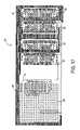
- FIG. 1is an elevation view of a high-density circuit module devised in accordance with a preferred four-high embodiment of the present invention.
- FIG. 2is an elevation view of a stacked high-density circuit module devised in accordance with a preferred two-high embodiment of the present invention.
- FIG. 3depicts, in enlarged view, the area marked “A” in FIG. 2 .
- FIG. 4depicts in enlarged view, the area marked “B” in FIG. 2 .
- FIG. 5is an enlarged depiction of an exemplar connection area in a stacked module devised in accordance with a preferred embodiment.
- FIG. 6depicts a flexible circuit connective set of flex circuits that has a single conductive layer.
- FIG. 7depicts a four-high stacked module mounted on a memory expansion board in accordance with a preferred embodiment of the present invention.
- FIG. 8depicts a memory expansion board or DIMM mounted with four-high modules.
- FIG. 9depicts a memory system devised in accordance with the present invention.
- FIG. 10is an elevation view of a module illustrating features of an alternative preferred embodiment of the present invention.
- FIG. 11is an elevation view of a module depicting features of an alternative preferred embodiment of the present invention.
- FIG. 12is an elevation view of a module depicting features of an alternative preferred embodiment.
- FIG. 13is another view depicting features of an alternative preferred embodiment of the present invention.
- FIG. 14is an elevation view of a module that depicts an alternative preferred embodiment of the present invention.
- FIG. 15depicts, in enlarged view, the area marked “C” in FIG. 14 .
- FIG. 16depicts in enlarged view, an alternative connection strategy between constituent elements of a module and a flex in a preferred embodiment in accordance with the present invention.
- FIG. 17depicts an exemplar first conductive layer of a flex employed in a preferred embodiment of the invention.
- FIG. 18depicts an exemplar second conductive layer of a flex employed in a preferred embodiment of the invention.
- FIG. 19depicts another alternative embodiment of the present invention.
- FIG. 20is a side view of the embodiment of the invention depicted in FIG. 19 taken along the direction of the arrow marked 200 .
- FIG. 21depicts an early assembly stage of another embodiment of the present invention.
- FIG. 22depicts an assembly stage, later than that depicted in FIG. 21 , of another embodiment of the present invention.
- FIG. 23depicts an assembly stage, later than that depicted in FIG. 22 , of another embodiment of the present invention.
- FIG. 24depicts an assembly stage, later than that depicted in FIG. 23 , of another embodiment of the present invention.
- FIG. 25depicts an early assembly stage of yet another embodiment of the present invention.
- FIG. 26depicts an assembly stage, later than that depicted in FIG. 25 , of another embodiment of the present invention.
- FIG. 27depicts an assembly stage, later than that depicted in FIG. 26 , of another embodiment of the present invention.
- FIG. 28depicts an assembly stage, later than that depicted in FIG. 27 , of another embodiment of the present invention.
- FIG. 29depicts an early assembly stage of yet another embodiment of the present invention.
- FIG. 30depicts an assembly stage, later than that depicted in FIG. 29 , of another embodiment of the present invention.
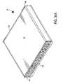
- FIG. 31depicts the alternative embodiment of the present invention depicted in FIG. 30 , from another perspective slightly below module 10 .
- FIG. 32depicts an early assembly stage of another embodiment of the present invention.
- FIG. 33depicts an assembly stage, later than that depicted in FIG. 32 , of another embodiment of the present invention.
- FIG. 34depicts an assembly stage, later than that depicted in FIG. 33 , of another embodiment of the present invention
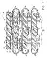
- FIG. 1is an elevation view of module 10 devised in accordance with a preferred embodiment of the present invention.
- Module 10is comprised of four CSPs: level four CSP 12 , level three CSP 14 , level two CSP 16 , and level one CSP 18 .
- Each of the CSPshas an upper surface 20 and a lower surface 22 and opposite lateral edges 24 and 26 and typically include at least one integrated circuit surrounded by a plastic body 27 .
- the bodyneed not be plastic, but a large majority of packages in CSP technologies are plastic.
- the present inventionmay be devised to create modules with different size CSPs and that the constituent CSPs may be of different types within the same module 10 .
- one of the constituent CSPsmay be a typical CSP having lateral edges 24 and 26 that have an appreciable height to present a “side” while other constituent CSPs of the same module 10 may be devised in packages that have lateral edges 24 and 26 that are more in the character of an edge rather than a side having appreciable height.
- CSPchip scale packaged integrated circuits
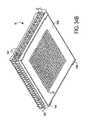
- FIGS. 1 and 2are depicted with CSPs of a particular profile known to those in the art, but it should be understood that the figures are exemplary only.
- Typical CSPssuch as, for example, ball-grid-array (“BGA”), micro-ball-grid array, and fine-pitch ball grid array (“FBGA”) packages have an array of connective contacts embodied, for example, as leads, bumps, solder balls, or balls that extend from lower surface 22 of a plastic casing in any of several patterns and pitches. An external portion of the connective contacts is often finished with a ball of solder. Shown in FIG. 1 are contacts 28 along lower surfaces 22 of the illustrated constituent CSPs 12 , 14 , 16 , and 18 . Contacts 28 provide connection to the integrated circuit or circuits within the respective packages.
- BGAball-grid-array
- FBGAfine-pitch ball grid array
- module 10may be devised to present a lower profile by stripping from the respective CSPs, the balls depicted in FIG. 1 as contacts 28 and providing a connection facility at contact 28 that results from solder paste that is applied either to the pad contact of the CSP that is typically present under or within the typical ball contacts provided on CSP devices or to the contact sites on the flex circuitry to be connected to contact 28 .
- flex circuits(“flex”, “flex circuits” or “flexible circuit structures”) 30 and 32 are shown connecting various constituent CSPs. Some embodiments may employ more than one flex.
- the entire flex circuitmay be flexible or, as those of skill in the art will recognize, a PCB structure made flexible in certain areas to allow conformability in some areas and rigid in other areas for planarity along contact surfaces may be employed as an alternative flex circuit in the present invention. For example, structures known as rigid-flex may be employed.
- Form standard 34is shown disposed adjacent to upper surface 20 of each of the CSPs below level four CSP 12 .
- Form standard 34may be fixed to upper surface 20 of the respective CSP with an adhesive 35 which preferably is thermally conductive.
- Form standard 34may also, in alternative embodiments, merely lay on upper surface 20 or be separated from upper surface 20 by an air gap or medium such as a thermal slug or non-thermal layer.
- form standard 34may be inverted relative to the corresponding CSP so that, for example, it would be opened over the upper surface 20 of CSP 18 .
- a form standardmay be employed on each CSP in module 10 for heat extraction enhancement.
- form standard 34is a thermally conductive material such as the copper that is employed in a preferred embodiment, layers or gaps interposed between form standard 34 and the respective CSP (other than thermally conductive layers such as adhesive) are not highly preferred.
- Form standard 34is, in a preferred embodiment, devised from copper to create, as shown in the depicted preferred embodiment of FIG. 1 , a mandrel that mitigates thermal accumulation while providing a standard sized form about which flex circuitry is disposed.
- Form standard 34may take other shapes and forms such as for example, an angular “cap” that rests upon the respective CSP body or as another example, it may be folded to increase its cooling surface area while providing an appropriate axial form for the flex that is wrapped about a part of form standard 34 as shown in later FIG. 14 . It also need not be thermally enhancing although such attributes are preferable.
- the form standard 34allows the invention to be employed with CSPs of varying sizes, while articulating a single set of connective structures useable with the varying sizes of CSPs.
- a single set of connective structuressuch as flex circuits 30 and 32 (or a single flexible circuit in the mode where a single flex is used in place of the flex circuit pair 30 and 32 ) may be devised and used with the form standard 34 method and/or systems disclosed herein to create stacked modules with CSPs having different sized packages.
- portions of flex circuits 30 and 32are fixed to form standard 34 by adhesive 35 which is preferably a tape adhesive, but may be a liquid adhesive or may be placed in discrete locations across the package.
- adhesive 35is thermally conductive.
- flex circuits 30 and 32are multi-layer flexible circuit structures that have at least two conductive layers. Other embodiments may, however, employ flex circuitry, either as one circuit or two flex circuits, that have only a single conductive layer.
- the conductive layersare metal such as alloy 110 .
- the use of plural conductive layersprovides advantages and the creation of a distributed capacitance across module 10 intended to reduce noise or bounce effects that can, particularly at higher frequencies, degrade signal integrity, as those of skill in the art will recognize.
- Module 10 of FIG. 1has plural module contacts 38 collectively identified as module array 40 . Connections between flex circuits are shown as being implemented with inter-flex contacts 43 which are shown as balls but may be low profile contacts constructed with pads and/or rings that are connected with solder paste applications to appropriate connections. Appropriate fills such as those indicated by conformal media reference 41 can provide added structural stability and coplanarity where desired. Media 41 is shown only as to CSPs 14 and 16 and only on one side to preserve clarity of view.
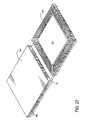
- FIG. 2shows a two-high module 10 devised in accordance with a preferred embodiment of the invention.
- FIG. 2has an area marked “A” that is subsequently shown in enlarged depiction in FIG. 3 and an area marked “B” that is shown subsequently in enlarged depiction in FIG. 4 .
- FIG. 3depicts in enlarged view, the area marked “A” in FIG. 2 .
- FIG. 3illustrates in a preferred embodiment, one arrangement of a form standard 34 and its relation to flex circuitry 32 in a two-high module 10 .
- the internal layer constructions of flex circuitry 32are not shown in this figure.
- adhesives 35 between flex circuit 32 and form standard 34are also shown in this figure.
- adhesive 35is not required but is preferred and the site of its application may be determined as being best for this embodiment in the area between CSPs with a smaller amount near the terminal point of form standard 34 as shown in FIG. 3 .
- Also shown in FIG. 3is an application of adhesive 36 between form standard 34 and CSP 18 .
- FIG. 4illustrates the connection between example contact 28 and module contact 38 through a lower flex contact 44 to illustrate a preferred solid metal path from level one CSP 18 to module contact 38 and, therefore, to an application PWB or memory expansion board to which the module is connectable.
- lower flex contact 44is preferably comprised from metal at the level of second conductive layer 58 interior to second outer surface 52 . As those of skill in the art will understand, heat transference from module 10 is thereby encouraged.
- Flex circuitry 30is shown in FIG. 4 to be comprised of multiple layers. This is merely an exemplar flexible circuitry that may be employed with the present invention. Single conductive layer and other variations on the described flexible circuitry may, as those of skill will recognize, be employed to advantage in the present invention.
- Flex circuitry 30has a first outer surface 50 and a second outer surface 52 . Flex circuit 30 has at least two conductive layers interior to first and second outer surfaces 50 and 52 . There may be more than two conductive layers in flex circuitry 30 and flex 32 . In the depicted preferred embodiment, first conductive layer or plane 54 and second conductive layer or plane 58 are interior to first and second outer surfaces 50 and 52 . Intermediate layer 56 lies between first conductive layer 54 and second conductive layer 58 . There may be more than one intermediate layer, but one intermediate layer of polyimide is preferred.
- FIG. 5is an enlarged depiction of an exemplar area around a lower flex contact 44 in a preferred embodiment.
- Windows 60 and 62are opened in first and second outer surface layers 50 and 52 respectively, to provide access to particular lower flex contacts 44 residing at the level of second conductive layer 58 in the flex.
- the upper flex contacts 42are contacted by contacts 28 of second level CSP 16 .
- lower flex contacts 44 and upper flex contacts 42are particular areas of conductive material (preferably metal such as alloy 110 ) at the level of second conductive layer 58 in the flex.
- Upper flex contacts 42 and lower flex contacts 44are demarked in second conductive layer 58 and may be connected to or isolated from the conductive plane of second conductive layer 58 . Demarking a lower flex contact 44 from second conductive layer 58 is represented in FIG. 5 by demarcation gap 63 shown at second conductive layer 58 . Where an upper or lower flex contact 42 or 44 is not completely isolated from second conductive layer 58 , demarcation gaps do not extend completely around the flex contact.
- Contacts 28 of first level CSP 18pass through a window 60 opened through first outer surface layer 50 , first conductive layer 54 , and intermediate layer 56 , to contact an appropriate lower flex contact 44 .
- Window 62is opened through second outer surface layer 52 through which module contacts 38 pass to contact the appropriate lower flex contact 44 .
- Respective ones of contacts 28 of second level CSP 16 and first level CSP 18are connected at the second conductive layer 58 level in flex circuits 30 and 32 to interconnect appropriate signal and voltage contacts of the two CSPs.
- respective contacts 28 of second level CSP 16 and first level CSP 18 that convey ground (VSS) signalsare connected at the first conductive layer 54 level in flex circuits 30 and 32 by vias that pass through intermediate layer 56 to connect the levels as will subsequently be described in further detail.
- CSPs 16 and 18are connected. Consequently, when flex circuits 30 and 32 are in place about first level CSP 18 , respective contacts 28 of each of CSPs 16 and 18 are in contact with upper and lower flex contacts 42 and 44 , respectively. Selected ones of upper flex contacts 42 and lower flex contacts 44 are connected. Consequently, by being in contact with lower flex contacts 44 , module contacts 38 are in contact with both CSPs 16 and 18 .
- module contacts 38pass through windows 62 opened in second outer layer 52 to contact lower CSP contacts 44 .
- module 10will exhibit a module contact array that has a greater number of contacts than do the constituent CSPs of module 10 .
- some of module contacts 38may contact lower flex contacts 44 that do not contact one of the contacts 28 of first level CSP 18 but are connected to contacts 28 of second level CSP 16 . This allows module 10 to express a wider datapath than that expressed by the constituent CSPs.
- a module contact 38may also be in contact with a lower flex contact 44 to provide a location through which different ICs in the module may be enabled when no unused contacts are available or convenient for that purpose.
- first conductive layer 54is employed as a ground plane, while second conductive layer 58 provides the functions of being a signal conduction layer and a voltage conduction layer.
- first and second conductive layersmay be reversed with attendant changes in windowing and use of commensurate interconnections.
- FIG. 6depicts a flexible circuit connective set of flex circuits 30 and 32 that has a single conductive layer 64 .
- flex circuits 30 and 32extend further than shown and have portions which are, in the construction of module 10 brought about the curvature areas 66 of form standard 34 that mark the lateral extent of this example of a preferred form standard and are then disposed above the body of CSP 18 or the respective CSP of the module and therefore, the form standard.
- first and second outer layers 50 and 52 and intermediate layer 56there are shown in this single conductive layer flex embodiment of module 10 .
- FIG. 6are a set of single layer lower flex contacts 68 demarked at the level of conductive layer 64 .
- Form standard 34is shown attached to the body 27 of first level CSP 18 through an adhesive. In some embodiments, it may also be positioned to directly contact body 27 of the respective CSP.
- Form standard 34may take many different configurations to allow a connective flex circuitry to be prepared exhibiting a single set of dimensions which may, when used in conjunction with form standard 34 , be employed to create stacked modules 10 from CSPs of a variety of different dimensions. In a preferred embodiment, form standard 34 will present a lateral extent broader than the upper major surface of the CSP over which it is disposed. Thus, the CSPs from one manufacturer may be aggregated into a stacked module 10 with the same flex circuitry used to aggregate CSPs from another manufacturer into a different stacked module 10 despite the CSPs from the two different manufacturers having different dimensions.
- heat transferencecan be improved with use of a form standard 34 comprised of heat transference material such as a metal or preferably, copper or a copper compound or alloy to provide a significant sink for thermal energy.
- a form standard 34comprised of heat transference material such as a metal or preferably, copper or a copper compound or alloy to provide a significant sink for thermal energy.
- Such thermal enhancement of module 10particularly presents opportunities for improvement of thermal performance where larger numbers of CSPs are aggregated in a single stacked module 10 .
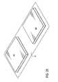
- FIG. 7depicts a four-high stacked module 10 mounted on a memory expansion board 70 in accordance with a preferred embodiment of the present invention.
- expansion board 70 shown in FIG. 7has a set of contacts along one edge that as depicted are set in socket connector 72 . Those contacts connect module 10 to a logic system on or connected to board 74 on which expansion board 70 is mounted. It should be understood that in a preferred embodiment of the memory expansion system and method provided herein, expansion board 70 will be populated with nine such modules 10 per side for a total of 72 devices if the stacked modules are each comprised from four devices.
- FIG. 8depicts memory expansion board 70 mounted with four-high modules 10 .
- using four-high stacked modules on expansion board 70reduces the interconnect length for the number of devices accessed but increase the total number of devices and, therefore, the impedance and particularly, the capacitive loading presented by a densely populated DIMM board.
- FIG. 9depicts a memory system 80 devised in accordance with the present invention.
- system 80is employed with stacked modules 10 devised in accordance with the present invention.
- the preferred embodimentis for a DDRII registered DIMM populated with 4 high stacked modules 10 although it may be employed with an equivalent number of DRAMs, i.e., 72 devices of either leaded or CSP packaging aggregated in stacks of any number of levels.
- Chipset 82 depicted in FIG. 9typically includes a microprocessor or memory controller that controls the memory access with system 80 .
- Clock 84is provided to decode logic 86 on each of depicted memory expansion boards 70 (1) , 70 (2) , 70 (3) , and 70 (4) .
- system 80 and its methodsmay be employed with one or more DIMMs or other memory expansion boards 70 . It may also be employed off a memory expansion board to access separately, the integrated circuits from which stacked circuit modules are comprised.
- Decode logic 86 on each of memory expansion boards 70 (1) , 70 (2) , 70 (3) , and 70 (4)provides a decoding of the respective CS signals provided to the respective memory expansion boards 70 as shown in FIG. 9 .
- the particular interconnection employed in the systemshould preferably be devised to minimize and balance power consumption across the circuit modules employed in the system.
- CS 0 , CS 1 , CS 2 , and CS 3are provided to memory expansion board 70 (1) from chipset 82 while CS 4 , CS 5 , CS 6 , and CS 7 are provided to memory expansion board 70 (2) as are CS 8 , CS 9 , CS 10 , and CS 11 provided to memory expansion board 70 (3) and CS 12 , CS 13 , CS 14 , and CS 15 are provided to memory expansion board 70 (4) .
- memory expansion boards 70are populated with nine four high CSP modules 10 per side.
- the depiction of FIG. 9shows, however, only one module 10 per memory expansion board 70 to preserve clarity of the view.
- the shown module 10is exploded to depict the four levels of module 10 which, in a preferred construction of module 10 include CSPs 18 , 16 , 14 , and 12 with the form standard 34 .
- decode logic 86may, on the appropriate signal from clock 84 , generate a level select signal which, in a preferred embodiment, is a multi-bit signal that controls a multiplexing switch 90 associated with several data lines.
- Switch 90is, in a preferred embodiment, a high speed switch and a FET muliplexer would provide a preferred multiplexing switch 90 in the practice of a preferred mode of the invention.
- the fan-out of multiplexing switch 90may be any that provides a selection capability to a variety of device data lines from a DQ line from chipset 82 .
- the DQ lines between chipset 82 and switches 90are depicted by double-headed arrows 94 ( 1 ), 94 ( 2 ), 94 ( 3 ) and 94 ( 4 ).
- multiple multiplexing switches 90are employed in practice of the depicted preferred embodiment of the invention.
- the number of multiplexing switches 90will depend upon the fan-out ratios. For example, use of nine 8:32 multiplexing switches 90 would be preferred (if available) or 4:8 or 1:4 multiplexing switches 90 will also provide advantages as an example. It should be understood that there are merely examples and that a variety of multiplexing switches and ratios may be employed for multiplexing switches 90 , although the type of switch and the ratios will affect the loading figures. Consequently, a FET mux is preferred for multiplexing switch 90 and a ratio of 1:4 is one of the preferred ratios to employ.
- FIG. 9The depiction in FIG. 9 is illustrative only and not meant to be limiting.
- a single DIMM board or expansion board 70may be employed in a system 80 in accordance with the present invention as well as larger numbers of expansion boards 70 .
- the number of expansion boards 70 that may function in system 80is partially a function of the access speeds required and the signal conformity.
- An exemplar multiplexing switch 90has multiple inputs 92 ( a ), 92 ( b ), 92 ( c ), and 92 ( d ) to provide independent data lines for each level of an exemplar module 10 populated upon the respective memory expansion board 70 .
- a 1:4 switch 90there will be 18 iterations of multiplexing switch 90 , one for each of the 18 four-high module 110 's populating memory expansion board 70 ( 1 ).
- the system 80 shown in FIG. 9presents a total of 288 memory devices. It should be noted that system 80 may be employed with ICs of any package type and need not be limited to DDR or DDRII or even CSP.
- the data line of each level of the constituent CSPs of each module 10is connected to one input 92 of a corresponding exemplar multiplexing switch 90 .
- multiplexing switch 90connects the appropriate one of the DQ signals 94 to one of the four levels of a module 10 on that memory expansion board 70 .
- This switching of the data bus through multiplexing switch 90may, in some systems, required further control signal connections as those of skill in the art will recognize to accommodate the data latency of one or more clocks cycles, CAS latency, and burst length, for example.
- expansion board 70may keep all the constituent devices of the modules 10 as if each constituent device of the modules 10 were the target, instead of having to switch terminations each time a different CS is chosen. In some applications it may be preferred to terminate the end of the data line past the last DIMM expansion board 70 . Other features may enable improvements to the efficiency of system 80 such as creating more CS banks by decoding the chip select lines.
- the capacitive load presented to chipset 82would be approximately the combination of the input capacitance of switching multiplexer 90 times the number of DIMM slots plus one DRAM device load plus one times the output capacitance of the multiplexing switch 90 . In large systems, this will reduce capacitive loading by a notable amount, thus allowing more DIMM slots at higher speeds and/or more densely populated DIMMs.
- Memory access system 80provides an opportunity to improve high speed memory performance and allows use of memory expansion configurations that might not otherwise be available due to capacitive loading in conventional DIMM systems.
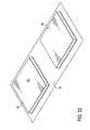
- FIG. 10is an elevation view of a module that depicts features of an alternative preferred embodiment of the present invention.
- the depicted module 10is comprised of a base element 120 and support elements 140 and 160 .
- base element 120 and support elements 140 and 160are shown as CSP devices, but the invention is not limited to arrangements of CSPs and may be employed to aggregate a variety of package types.
- Base element 120 and support elements 140 and 160each have, in the depicted embodiment, upper surfaces 20 and lower surfaces 22 and peripheral or lateral sides or edges 24 and 26 that may be in the character of sides or may, if the CSP is especially thin, be in the character of an edge.
- FIG. 10depicts base element 120 and support elements 140 and 160 in a stacked disposition with upper major surfaces of the constituent elements being proximally located in this back to back configuration. Between upper surfaces 20 of support elements 140 and 160 and upper surface 20 of base element 120 is shown adhesive layer 35 shown in exaggerated scale for clarity of depiction. Contacts 28 are emergent from lower surface 22 of base element 120 and support elements 140 and 160 . Module contacts 38 are shown depicted along the bottom of module 10 and provide connection for the module to a PWB or PCB or other mounting site.
- Support elements 140 and 160are preferably fixed to upper surface 20 of base element 120 by adhesive 35 which is shown as a tape adhesive, but may be a liquid adhesive or may be placed in discrete locations across the package.
- adhesive 35is thermally conductive.
- Adhesives that include a fluxmay be used to advantage in assembly of module 10 .
- Layer 35may also be a thermally conductive medium to encourage heat flow between the elements of module 10 .
- a mechanical clamp or clampsmay be used to hold the base and support elements together.
- the contacts for the module itselfmay be closer to either the base element or the support element(s) of the module although more typically and preferably, the module contacts will be closer to the base element.
- the support elementsmay also extend over the edges of the base element or may be disposed within the perimeter of the base element.
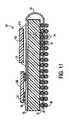
- FIG. 11illustrates the aggregation of a leaded package device having leads 310 (i.e., as support element 160 in this embodiment) with base element 120 and support element 140 .
- FIG. 11further depicts the placement of flex circuitry 30 attached to the upper side of base element 120 with the placement of support elements 140 and 160 in a position relatively above flex circuitry 30 rather than below as earlier shown in FIG. 10 .
- Flex circuitry 30is preferably attached to upper surface 20 of base element 120 with a thermally conductive adhesive depicted by reference 35 in FIG. 11 .
- a conformal media 41is indicated in FIG. 11 as being placed between contacts 28 to assist in creating conformality of structural areas of module 10 .
- conformal media 41is thermally conductive and is placed along the lower surface 22 of base element 120 although to preserve clarity of the view, its placement between only a few contacts 28 of base element 120 is shown in FIG. 11 .
- FIG. 12depicts another alternative embodiment of the present invention. Shown are base element 120 and support element 140 . In the place of previously shown single package support element 160 is leaded stack 170 , consisting of upper IC 190 and lower IC 210 .
- FIG. 13depicts a module that employs a CSP base element 120 and CSP support elements 140 and 160 interconnected with flex circuitry 30 .
- Heat sink 340is disposed between base element 120 and support elements 140 and 160 . As shown in FIG. 13 , heat sink 340 is in contact with a portion of casing 36 of an application in which module 10 is employed.
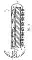
- FIG. 14is an alternative preferred embodiment of the present invention. Depicted in FIG. 14 are base element 120 and support elements 140 and 160 with all of the depicted ICs being packaged in CSP with support elements 140 and 160 extending beyond the physical boundaries of base element 120 .
- Form standard 34provides a standard form about which flex circuit 30 arcs. As earlier described, form standards may take a variety of forms and, in this embodiment, form standard 34 is folded to increase cooling surface area while providing an appropriate axial circumference and standard form for flex circuitry 30 . Also shown is extensive and preferred use of conformal underfill 41 .
- FIG. 15illustrates in enlarged perspective, detail of the area marked “C” in FIG. 14 and illustrates an exemplar connection between example contacts 28 of a support element and support flex contacts 57 of flex circuitry 30 .
- support flex contacts 57are shown as being at the level of first conductive layer 54 of flex circuitry 30 .
- FIG. 15illustrates a via 59 between the support flex contact 57 in contact with the right-most depicted contact 28 and second conductive layer 58 .
- the use of vias between conductive layer levelsallows flexibility in strategies employed to connect base element 120 with support elements and allows, for example, the connection of a contact from support elements 140 or 160 to a selected module contact 38 .
- support elements 140 and/or 160will have signals that are not directly connected to base element 120 , but which have functionality relevant to the operation of entire module 10 .
- a module contact 38provides that signal connection to support element 140 or 160 without a corresponding direct connection to base element 120 .
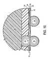
- Such a connection strategyis shown in FIG. 16 .
- FIG. 17illustrates an abstraction of the plot employed for the conductive areas at the level of first conductive plane 54 for a preferred embodiment similar to that depicted in FIG. 14 .
- the connective fields identified with references 65roughly correspond to connective areas for support element 140 while connective fields identified with references 67 roughly correspond to support element 160 as shown in FIG. 14 .
- Connective field 69provides connections for base element 120 .
- the connective fields 65 and 67provide support flex contacts 57 as well as traces that, combined with vias 59 , provide part of the connective facility for interconnecting support elements 140 and 160 to base element 120 .
- the viewis abstracted with many of the actual routing lines removed to assist in the clarity of the view.
- FIG. 18illustrates an abstraction of the routing plot employed for conductive areas at the level of second conductive surface or plane 58 for a preferred embodiment similar to that depicted in FIG. 14 .
- FIGS. 17 and 18employed to connect base element 120 , there is illustrated an example of using vias 59 to more fully employ the two conductive layers of the preferred embodiments.
- Connective fields 55 and 61indicate vias 59 as well as traces (that are not shown in the depiction for clarity of view) that provide part of the connective facility for interconnecting support elements 140 and 160 to base element 120 .
- base element 120On the depiction of FIG. 18 , there is found the identification of a lower flex contact 44 that may be employed by base element 120 .
- base element 120has a contact 28 that passes through window 60 and therefore, first conductive layer 54 to contact the identified lower flex contact 44 at the level of the second conductive layer as shown in FIG. 18 . It should be understood that this is a heuristic explanation and meant to be merely an example illustrating a feature found in some preferred embodiments of the invention.
- the identified lower flex contact 54 at the level of second conductive layer 58is connected to a via 59 by a trace 71 .
- Via 59passes in a relatively upward direction toward the body of base element 120 .
- via 59passes upwardly through flex circuitry 30 , it contacts a conductive area at the level of first conductive layer 54 as shown in FIG. 17 by the identification of via 59 in the field 69 .
- the identified via 59is then connected to trace 73 that provides a connection network to a variety of other contacts in the depicted embodiment.
- the use of two conductive layersis given an added flexibility by the illustrated use of vias through an intermediate layer.
- Vias that route through intermediate layer 56 to interconnect traces or flex contacts or conductive areas at different conductive layersmay be “on-pad” or coincident with the support or base flex contact to which they are connected. Such vias may also be “off-pad” and located near windows associated with the flex contacts from which signals are to be conveyed to another conductive layer. This provides added flexibility to connection schemes and layout routing.
- FIG. 19depicts another alternative embodiment of the present invention. Depicted in FIG. 19 are base element 120 with support element 140 in an inverted position with respect to base element 120 .
- Form standard 34is shown positioned between base element 120 and support element 140 (referred to together, with reference to this embodiment, “the depicted CSPs”), with radiating form portions 192 extending upwards and downwards in an area outside the lateral extent of base element 120 .
- radiating form portions 192may take various shapes and forms.
- radiating form portions 192extend partially around the circumference of the depicted CSPs, base element 120 and support element 140 , or may be disposed only on one or more lateral sides of the depicted CSPs or may extend fully around the circumference of the depicted CSPs.
- radiating form portions 192may have voids or fins or other non-contiguous features devised to increase their surface area.
- heat spreader portion 194is a central portion of form standard 34 , which is disposed between the depicted CSPs and may extend past the lateral extent of one or both of the designated ICs, as shown by the dotted lines.
- Heat spreader portion 194 and radiating form portions 192may be composed of similar materials or they may be composed of a different suitable heat-conducting materials. Further heat spreader portion 194 and radiating form portions 192 may be made in a variety of ways.
- the depicted IC'smay first be attached to flex circuitry 30 in a flat configuration with a radiating form portion 192 placed about each depicted IC, then heat spreader portion 194 placed atop base element 120 and the selected radiating for portion 192 , and affixed with adhesive or other suitable attachment methods such as, for example, tape adhesive, liquid adhesive, soldering, welding, or clamping. Subsequently, flex circuitry 30 may be folded to produce the relative positions shown in FIG. 19 . Adhesive or other suitable attachment methods may be used to secure radiating form portion 192 associated with support element 140 to heat spreader portion 194 .
- radiating form portions 192 and heat spreader portion 194may be separate pieces that are placed adjacent to each other in a manner devised to achieve a form standard 34 . Further, as those of skill will understand, in an alternative embodiment, radiating form portions 192 may be disposed around one or both of the depicted CSPs without the presence of heat spreader 194 between the depicted CSPs.
- flex circuitry 30is connected to base element 120 through contacts 28 and wrapped around one side of form standard 34 to connect to contacts 28 of support element 140 .
- radiating form portions 192 of form standard 34have curved edges 196 devised to provide an appropriate axial form for the flex circuitry 30 that is wrapped about a part of form standard 34 .
- form standard 34is provided with mounting feet 198 which are disposed on radiating form portions 192 outside of the lateral extent of flex circuitry 30 .
- the use of conformal underfillis not shown to simplify the depiction, however some embodiments may use conformal underfill as described with reference to FIG. 14 .
- FIG. 20is a side view of the embodiment of the invention depicted in FIG. 19 taken along the direction of the arrow marked 200 .
- Flex circuitry 30is shown wrapped around the curved edges 196 of form standard 34 .
- Module contacts 38are provided on flex circuitry 30 for connection of module 10 to its operating environment.
- flex circuitry 30is a multi-layer flexible circuit structures that has at least two conductive layers. Other embodiments may, however, employ flex circuitry, either as one circuit or two flex circuits, that have only a single conductive layer.
- Mounting feet 198extend outside of the lateral extent of flex circuitry 30 in a manner devised to provide stability and mechanical connectivity of module 10 to its operating environment.
- FIGS. 21-24depict another embodiment of the present invention in the process of assembly.
- FIG. 21depicts an early assembly stage of another embodiment of the present invention.
- Base element 120 and support element 140are preferably CSPs.
- Flex circuit 30is shown with base element 120 and support element 140 connected.
- the connectionis achieved by a variety of means be achieved by other means such as, for example, soldering, solder paste with later reflow, adhesives, laminate adhesives, and/or combinations of these and other known connection schemes.
- base element 120 and support element 140may, in other embodiments, be attached at a later stage and may at this stage be held in place with other schemes such as, for example, adhesive or pastes.
- FIG. 22depicts an assembly stage, later than that depicted in FIG. 21 , of another embodiment of the present invention. While a preferred scheme of assembling an exemplar embodiment of the invention is depicted by this and related Figures, the order is not limiting and, as those of skill will realize after appreciating this specification, various embodiments of the present invention may be assembled in various orders.
- Base element 120has upper surface 224 .
- Radiating form portions 192are shown disposed around base element 120 and support element 140 (“the depicted CSPs”). In this embodiment, radiating form portions 192 have heat radiating fins 222 formed therein. Preferably, there is thermal conduction between radiating form portions 192 and the depicted CSPs.
- radiating form portions 192may placed adjacent to or in contact with the depicted CSPs, or may be attached by adhesive, or interference fit, or may be attached to flex circuitry 30 . In other embodiments, radiating form portions 192 may be near but not touch the depicted CSPs. A distance ‘D’ separates the proximal edges of radiating form portions 192 . Distance D is devised to facilitate folding of flex at a later stage of assembly of module 10 . In certain embodiments, distance D may be devised by finding the added height of form portions 192 or of the depicted CSPs, whichever is greater.
- This summed heightmay be increased by the height of heat spreader portion 194 , if the particular embodiment contains a heat spreader portion 194 . Further, distance D may be increased by factors such as the additional distance needed to wrap about curved edges 196 (an example of which is described with reference to FIG. 24 ), or ‘slack’ needed for folding and assembly, if any, or desired ‘slack’ after assembly, if any.
- FIG. 23depicts an assembly stage, later than that depicted in FIG. 22 , of another embodiment of the present invention.
- heat spreader portion 194is shown placed on upper surface 224 of base element IC 120 .
- form standard 34may be assembled in a different order, such as, for example, placing heat spreader portion 194 of form standard 34 on either of the depicted CSPs or, as an another alternative exemplar assembly order, placing two or more pieces on top of either or both of the depicted CSPs.
- Heat spreader portion 194 of form standard 34may be fixed to upper surface 224 of the respective CSP with an adhesive which preferably is thermally conductive.
- Heat spreader portion 194may also, in alternative embodiments, merely lay on upper surface 224 or be separated from upper surface 224 by an air gap or medium such as a thermal slug or non-thermal layer.
- the lateral extent of heat spreader portion 194is preferably greater than the lateral extent of one or both of the depicted CSPs, and preferably, in this embodiment, equal to the largest lateral extent of radiating form portions 192 in each lateral direction. However, in other embodiments, the lateral extent of heat spreader portion 194 may be greater than that of radiating form portions 192 in either direction or less than that of the depicted CSPs in either direction.
- FIG. 24depicts an assembly stage, later than that depicted in FIG. 23 , of another embodiment of the present invention.
- the depiction in FIG. 24( a )is from a perspective slightly above module 10 , viewed after flex circuitry 30 has been folded to place support element 140 in a stacked, inverted position over base element 120 .
- flex circuitry 30is depicted with a portion in a curved disposition over curved edges 196 of radiating form portions 192 .
- Module 10may be secured in this configuration by a number of schemes such as, for example, adhesive, laminate adhesive, and soldering.
- the depiction in FIG. 24( b )is from a perspective slightly below module 10 .
- Mounting feet 198are depicted extending from radiating form portions 192 .
- Module contacts 38are present on the bottom surface 242 of module 10 for connection of module 10 to its operating environment.
- mounting feet 198are sized such that they extend the same distance as module contacts 38 in a perpendicular direction from bottom surface 242 . In other embodiments, however, mounting feet may extend less or more than module contacts 38 .
- FIGS. 25-28depict another embodiment of the present invention in various stages of assembly.
- FIG. 25depicts an early assembly stage of yet another embodiment of the present invention. This stage is similar to that described with regard to FIG. 21 , with base element 120 and support element 140 attached to flex circuitry 30 .
- FIG. 26depicts an assembly stage, later than that depicted in FIG. 25 , of another embodiment of the present invention. While a preferred scheme of assembling an exemplar embodiment of the invention is depicted by this and related Figures, the order is not limiting and, as those of skill will realize after appreciating this specification, various embodiments of the present invention may be assembled in various orders.
- Base element 120has upper surface 224 .
- Radiating form portions 192are shown disposed around base element 120 and support element 140 (“the depicted CSPs”). The separation distance D and the connection of radiating form portions 194 to flex circuitry 30 and may follow the description made with regard to FIG. 22 .
- radiating form portions 194 of form standard 34are metal pieces with form curves 262 and form tabs 264 , which will be further described with reference to FIG. 27 .
- radiating form portions 194may be made of suitably rigid and heat conducting materials such as, for example, various metals, alloys, and composites.
- FIG. 27depicts an assembly stage, later than that depicted in FIG. 25 , of another embodiment of the present invention.
- heat spreader portion 194is made of copper and has a thickness of approximately 1 mm. The depiction in FIG. 27 has the same orientation as that in FIG. 26 .
- heat spreader portion 194is shown placed on upper surface 224 of base element IC 120 .
- Heat spreader portion 194 of form standard 34may be fixed to upper surface 224 of the respective CSP with an adhesive which preferably is thermally conductive.
- Heat spreader portion 194may also, in alternative embodiments, merely lay on upper surface 224 or be separated from upper surface 224 by an air gap or medium such as a thermal slug or non-thermal layer.
- the lateral extent of heat spreader portion 194is preferably greater than the lateral extent of one or both of the depicted CSPs, and preferably, in this embodiment, greater than the largest lateral extent of radiating form portions 192 in each of the three lateral directions shown in which heat spreader portion 194 has a mount 272 .
- mount 272has thermally conductive properties.
- heat spreader portion 194has mounts 272 extending from three of its four sides. The fourth side, in this embodiment, has no mount 272 and instead presents a side edge 276 that is preferably flush with the outside edge presented by the adjacent form curve 262 .
- heat spreader 194touches form curve 262 in a manner devised to promote thermal conduction.
- Mounts 272preferably extend in a downward direction with respect to upper surface 224 of base element 120 ( FIG. 26 ), and preferably extend past the radiating form portions 192 .
- Flex circuitry 30has portion ‘F’ that is folded in a later stage of assembly from that depicted in FIG. 27 .
- Form tabs 264 of the radiating form element 192 that is underneath heat spreader 194are preferably in contact with the lower surface of heat spreader 194 (not visible in this depiction) in a manner devised to provide mechanical support and heat conductivity.
- FIG. 28depicts an assembly stage, later than that depicted in FIG. 27 , of another embodiment of the present invention.
- the depiction in FIG. 28( a )is from a perspective slightly above module 10 , viewed after flex circuitry 30 has been folded at portion F to place support element 140 in a stacked, inverted position over base element 120 .
- flex circuitry 30is depicted with a portion in a curved disposition over form curves 262 of radiating form portions 192 .
- Module 10may be secured in this configuration by a number of schemes such as, for example, adhesive, laminate adhesive, welding, clamping, and soldering.
- the depiction in FIG. 28( b )is from a perspective slightly below module 10 .
- Mounts 272are depicted extending from radiating form portions 192 .
- Module contacts 38are present on the bottom surface 242 of module 10 for connection of module 10 to its operating environment.
- mounts 272extend the same distance as module contacts 38 downward in a direction perpendicular to bottom surface 242 , but preferably outside the lateral extent of base element 120 . In other embodiments, however, mounts 272 may extend less or more than module contacts 38 depending on the packaging scheme and operating environment.
- Bottom mounting surfaces 274 of mounts 272are preferably soldered to a ground plane of the circuit board used in module 10 's operating environment.
- mounts 272have different shapes that extent in different directions and mounts 272 may be welded or soldered or rest on a variety of surfaces in module 10 's operating environment, such as, for example, circuit boards, mounts formed on circuit boards, chassis, walls or other interior surfaces of hermetic packaging containers, etc.
- module 10may be packaged in various forms of sealed electronic packages devised to provide high-reliability under severe operating conditions.
- FIGS. 29-31depict another embodiment of the present invention in various stages of assembly.
- FIG. 29depicts an early assembly stage of yet another embodiment of the present invention.
- flex circuitry 30flex circuitry 30 is has flex extensions 292 and 294 .
- Support elements 140 and 160are disposed on flex extension 292 and 294 , and may, at the depicted stage of assembly, be attached by various ways such as, for example, soldering, solder paste, adhesives, and laminate adhesives.
- FIG. 30depicts an assembly stage, later than that depicted in FIG. 29 , of another embodiment of the present invention. While a preferred scheme of assembling an exemplar embodiment of the invention is depicted by this and related Figures, the order is not limiting and, as those of skill will realize after appreciating this specification, various embodiments of the present invention may be assembled in various orders.
- flex extensions 292 and 294are depicted wrapped about form standard 34 .
- Base element 120not visible in this depiction, is underneath form standard 34 with its upper surface 224 adjacent to form standard 34 .
- form standard 34has folded portions 304 and 306 , devised to present support and heat absorption surfaces on which support elements 140 and 160 rest.
- support elements 140 and 160are inverted with respect to their depiction in FIG. 29 , due to the folding of flex extensions 292 and 294 .
- flex circuitry 30is shown with two flex extensions, this is not limiting and other embodiments may contain one or two or three or more flex extensions which may be devised to provide flexible circuit connectivity to each other and/or base element 120 and/or the operating environment of module 10 .
- form standard 34has two folded portions 304 and 306
- other embodimentsmay have one or two or three or more folded portions, and such portions may be devised to provide support and/or heat absorption for support elements 140 and 160 , and may be devised to present surfaces for attachment and/or support and/or heat absorption for support elements 140 and/or 160 that may be horizontal or vertical or disposed at other angles with respect to base element 120 .
- folded portions 304 and 306are shown in this embodiment, form standard 34 may be made in a folded configuration or be made of solid material or material shaped with voids of various shapes devised to provide heat radiation and/or ease of manufacturing.
- folded portion 206is shaped with a contour to provide for support elements 140 and 160 that may have different heights.
- Form standard 34has radiating portions 302 disposed partially around its outside edges.
- FIG. 31depicts the alternative embodiment of the present invention depicted in FIG. 30 , from another perspective slightly below module 10 .
- FIGS. 32-34depict another embodiment of the present invention in the process of assembly.
- FIG. 32depicts an early assembly stage of another embodiment of the present invention. Flex circuit 30 is shown with base element 120 and support element 140 connected.
- FIG. 33depicts an assembly stage, later than that depicted in FIG. 32 , of another embodiment of the present invention. While a preferred scheme of assembling an exemplar embodiment of the invention is depicted by this and related Figures, the order is not limiting and, as those of skill will realize after appreciating this specification, various embodiments of the present invention may be assembled in various orders.
- Radiating form portions 192are shown disposed around base element 120 and support element 140 (“the depicted CSPs”).
- heat spreader portion 194is shown placed on upper surface 224 of base element IC 120 and atop of the respective radiating form portion 192 .
- heat spreader portion 194is provided with radiating pins 332 , devised to present increased surface area for heat radiation and to provide mechanical support for form standard 34 and the assembled module 10 .
- those radiating pins 332 disposed about the interior portion of heat spreader 194are provided with flat internal edges 334 to provide a flush surface for placement in contact with or near support element 140 when flex circuitry 30 is folded (at a later stage of assembly) to place module 10 in its completed configuration.
- More radiating pins 332are provided underneath central surface 336 of heat spreading portion 194 .
- radiating pins 332are depicted as having uniform size and spacing, however, this is not limiting and radiating pins 332 may have different sizes and spacing, and may extend in different directions.
- FIG. 34depicts an assembly stage, later than that depicted in FIG. 33 , of another embodiment of the present invention.
- the depiction in FIG. 34( a )is from a perspective slightly above module 10 , viewed after flex circuitry 30 has been folded to place support element 140 in a stacked, inverted position over base element 120 .
- flex circuitry 30is depicted with a portion in a curved disposition over curved edges 196 of radiating form portions 192 .
- the depiction in FIG. 34( b )is from a perspective slightly below module 10 .
- Mounting feet 198are depicted extending from radiating form portions 192 .
- Module contacts 38are present on the bottom surface 242 of module 10 for connection of module 10 to its operating environment.
- radiating pins 332have flat edges 342 devised to present a flat profile at the lateral extent of module 10 .
- a flat profilemay enhance heat transfer characteristics when module 10 is placed in abutment to a wall of a packaging unit or other surface that may be present in the operating environment of module 10 .
Landscapes
- Engineering & Computer Science (AREA)
- Microelectronics & Electronic Packaging (AREA)
- Physics & Mathematics (AREA)
- Power Engineering (AREA)
- Condensed Matter Physics & Semiconductors (AREA)
- General Physics & Mathematics (AREA)
- Computer Hardware Design (AREA)
- Geometry (AREA)
- Structure Of Printed Boards (AREA)
- Semiconductor Memories (AREA)
- Cooling Or The Like Of Semiconductors Or Solid State Devices (AREA)
Abstract
Description
Claims (13)
Priority Applications (1)
| Application Number | Priority Date | Filing Date | Title |
|---|---|---|---|
| US11/221,597US7524703B2 (en) | 2001-10-26 | 2005-09-07 | Integrated circuit stacking system and method |
Applications Claiming Priority (5)
| Application Number | Priority Date | Filing Date | Title |
|---|---|---|---|
| US10/005,581US6576992B1 (en) | 2001-10-26 | 2001-10-26 | Chip scale stacking system and method |
| US10/453,398US6914324B2 (en) | 2001-10-26 | 2003-06-03 | Memory expansion and chip scale stacking system and method |
| PCT/US2003/029000WO2004109802A1 (en) | 2003-06-03 | 2003-09-15 | Memory expansion and integrated circuit stacking system and method |
| US10/814,532US6956284B2 (en) | 2001-10-26 | 2004-03-31 | Integrated circuit stacking system and method |
| US11/221,597US7524703B2 (en) | 2001-10-26 | 2005-09-07 | Integrated circuit stacking system and method |
Related Parent Applications (1)
| Application Number | Title | Priority Date | Filing Date |
|---|---|---|---|
| US10/814,532DivisionUS6956284B2 (en) | 2001-10-26 | 2004-03-31 | Integrated circuit stacking system and method |
Publications (2)
| Publication Number | Publication Date |
|---|---|
| US20060008945A1 US20060008945A1 (en) | 2006-01-12 |
| US7524703B2true US7524703B2 (en) | 2009-04-28 |
Family
ID=35125773
Family Applications (4)
| Application Number | Title | Priority Date | Filing Date |
|---|---|---|---|
| US10/814,532Expired - LifetimeUS6956284B2 (en) | 2001-10-26 | 2004-03-31 | Integrated circuit stacking system and method |
| US10/872,897AbandonedUS20040235222A1 (en) | 2001-10-26 | 2004-06-21 | Integrated circuit stacking system and method |
| US11/173,445Expired - LifetimeUS7595550B2 (en) | 2001-10-26 | 2005-07-01 | Flex-based circuit module |
| US11/221,597Expired - LifetimeUS7524703B2 (en) | 2001-10-26 | 2005-09-07 | Integrated circuit stacking system and method |
Family Applications Before (3)
| Application Number | Title | Priority Date | Filing Date |
|---|---|---|---|
| US10/814,532Expired - LifetimeUS6956284B2 (en) | 2001-10-26 | 2004-03-31 | Integrated circuit stacking system and method |
| US10/872,897AbandonedUS20040235222A1 (en) | 2001-10-26 | 2004-06-21 | Integrated circuit stacking system and method |
| US11/173,445Expired - LifetimeUS7595550B2 (en) | 2001-10-26 | 2005-07-01 | Flex-based circuit module |
Country Status (5)
| Country | Link |
|---|---|
| US (4) | US6956284B2 (en) |
| EP (1) | EP1730774A4 (en) |
| JP (1) | JP2007532004A (en) |
| CN (1) | CN1961421A (en) |
| WO (1) | WO2005098941A2 (en) |
Cited By (3)
| Publication number | Priority date | Publication date | Assignee | Title |
|---|---|---|---|---|
| US20090084597A1 (en)* | 2006-03-20 | 2009-04-02 | Sumitomo Bakelite Co., Ltd. | Circuit board and connection substrate |
| US20110266696A1 (en)* | 2008-03-03 | 2011-11-03 | Micron Technology, Inc. | Semiconductor device packages including a semiconductor device and a redistribution element |
| US20130044442A1 (en)* | 2010-01-19 | 2013-02-21 | Tristan Jobert | Sensor having damping |
Families Citing this family (78)
| Publication number | Priority date | Publication date | Assignee | Title |
|---|---|---|---|---|
| US7505862B2 (en)* | 2003-03-07 | 2009-03-17 | Salmon Technologies, Llc | Apparatus and method for testing electronic systems |
| US7408258B2 (en)* | 2003-08-20 | 2008-08-05 | Salmon Technologies, Llc | Interconnection circuit and electronic module utilizing same |
| US20050184376A1 (en)* | 2004-02-19 | 2005-08-25 | Salmon Peter C. | System in package |
| US7254036B2 (en) | 2004-04-09 | 2007-08-07 | Netlist, Inc. | High density memory module using stacked printed circuit boards |
| US20050255722A1 (en)* | 2004-05-07 | 2005-11-17 | Salmon Peter C | Micro blade assembly |
| WO2005119765A2 (en)* | 2004-06-02 | 2005-12-15 | Tessera, Inc. | Assembly including vertical and horizontal joined circuit panels |
| US7423885B2 (en) | 2004-09-03 | 2008-09-09 | Entorian Technologies, Lp | Die module system |
| US20060050492A1 (en) | 2004-09-03 | 2006-03-09 | Staktek Group, L.P. | Thin module system and method |
| US7324352B2 (en) | 2004-09-03 | 2008-01-29 | Staktek Group L.P. | High capacity thin module system and method |
| US7443023B2 (en) | 2004-09-03 | 2008-10-28 | Entorian Technologies, Lp | High capacity thin module system |
| US7511968B2 (en) | 2004-09-03 | 2009-03-31 | Entorian Technologies, Lp | Buffered thin module system and method |
| US7522421B2 (en) | 2004-09-03 | 2009-04-21 | Entorian Technologies, Lp | Split core circuit module |
| US7446410B2 (en)* | 2004-09-03 | 2008-11-04 | Entorian Technologies, Lp | Circuit module with thermal casing systems |
| US7289327B2 (en) | 2006-02-27 | 2007-10-30 | Stakick Group L.P. | Active cooling methods and apparatus for modules |
| US7606040B2 (en) | 2004-09-03 | 2009-10-20 | Entorian Technologies, Lp | Memory module system and method |
| US7542297B2 (en) | 2004-09-03 | 2009-06-02 | Entorian Technologies, Lp | Optimized mounting area circuit module system and method |
| US7616452B2 (en) | 2004-09-03 | 2009-11-10 | Entorian Technologies, Lp | Flex circuit constructions for high capacity circuit module systems and methods |
| US7579687B2 (en)* | 2004-09-03 | 2009-08-25 | Entorian Technologies, Lp | Circuit module turbulence enhancement systems and methods |
| US7606050B2 (en) | 2004-09-03 | 2009-10-20 | Entorian Technologies, Lp | Compact module system and method |
| US7468893B2 (en) | 2004-09-03 | 2008-12-23 | Entorian Technologies, Lp | Thin module system and method |
| US7760513B2 (en) | 2004-09-03 | 2010-07-20 | Entorian Technologies Lp | Modified core for circuit module system and method |
| US7606049B2 (en) | 2004-09-03 | 2009-10-20 | Entorian Technologies, Lp | Module thermal management system and method |
| US7163830B2 (en)* | 2004-10-12 | 2007-01-16 | Salmon Peter C | Method for temporarily engaging electronic component for test |
| US7427809B2 (en)* | 2004-12-16 | 2008-09-23 | Salmon Technologies, Llc | Repairable three-dimensional semiconductor subsystem |
| US7709943B2 (en)* | 2005-02-14 | 2010-05-04 | Daniel Michaels | Stacked ball grid array package module utilizing one or more interposer layers |
| US7675166B2 (en) | 2005-05-11 | 2010-03-09 | Maxim Integrated Products, Inc. | Integrated circuit package device comprising electrical contacts making solderless and bondless electrical-mechanical connection |
| US7033861B1 (en)* | 2005-05-18 | 2006-04-25 | Staktek Group L.P. | Stacked module systems and method |
| US20070023904A1 (en)* | 2005-08-01 | 2007-02-01 | Salmon Peter C | Electro-optic interconnection apparatus and method |
| US7586747B2 (en) | 2005-08-01 | 2009-09-08 | Salmon Technologies, Llc. | Scalable subsystem architecture having integrated cooling channels |
| US7442050B1 (en) | 2005-08-29 | 2008-10-28 | Netlist, Inc. | Circuit card with flexible connection for memory module with heat spreader |
| US7511969B2 (en) | 2006-02-02 | 2009-03-31 | Entorian Technologies, Lp | Composite core circuit module system and method |
| US8810018B2 (en)* | 2006-02-03 | 2014-08-19 | Stats Chippac Ltd. | Stacked integrated circuit package system with face to face stack configuration |
| US7619893B1 (en) | 2006-02-17 | 2009-11-17 | Netlist, Inc. | Heat spreader for electronic modules |
| US8803299B2 (en)* | 2006-02-27 | 2014-08-12 | Stats Chippac Ltd. | Stacked integrated circuit package system |
| US7829986B2 (en) | 2006-04-01 | 2010-11-09 | Stats Chippac Ltd. | Integrated circuit package system with net spacer |
| US7710735B2 (en)* | 2006-04-01 | 2010-05-04 | Stats Chippac Ltd. | Multichip package system |
| US20100148335A1 (en)* | 2006-06-06 | 2010-06-17 | Nec Corporation | Semiconductor package, method of manufacturing same, semiconductor device and electronic device |
| US7888185B2 (en) | 2006-08-17 | 2011-02-15 | Micron Technology, Inc. | Semiconductor device assemblies and systems including at least one conductive pathway extending around a side of at least one semiconductor device |
| US7425758B2 (en)* | 2006-08-28 | 2008-09-16 | Micron Technology, Inc. | Metal core foldover package structures |
| WO2008029813A1 (en)* | 2006-09-04 | 2008-03-13 | Nec Corporation | Wiring board composite body, semiconductor device, and method for manufacturing the wiring board composite body and the semiconductor device |
| US7691668B2 (en)* | 2006-12-19 | 2010-04-06 | Spansion Llc | Method and apparatus for multi-chip packaging |
| US8018723B1 (en) | 2008-04-30 | 2011-09-13 | Netlist, Inc. | Heat dissipation for electronic modules |
| GB2459751A (en)* | 2008-05-06 | 2009-11-11 | Ibm | Self contained memory subsystem |
| KR101485582B1 (en)* | 2008-08-13 | 2015-01-23 | 삼성전자주식회사 | Semiconductor package and manufacturing method thereof |
| US8385073B2 (en)* | 2009-07-08 | 2013-02-26 | Flextronics Ap, Llc | Folded system-in-package with heat spreader |
| US8670588B2 (en)* | 2009-09-08 | 2014-03-11 | Apple Inc. | Handheld device assembly |
| US8027162B2 (en)* | 2009-09-24 | 2011-09-27 | International Business Machines Corporation | Liquid-cooled electronics apparatus and methods of fabrication |
| US8541886B2 (en)* | 2010-03-09 | 2013-09-24 | Stats Chippac Ltd. | Integrated circuit packaging system with via and method of manufacture thereof |
| TWI406376B (en)* | 2010-06-15 | 2013-08-21 | Powertech Technology Inc | Semiconductor chip package |
| US9027360B2 (en) | 2011-05-06 | 2015-05-12 | International Business Machines Corporation | Thermoelectric-enhanced, liquid-based cooling of a multi-component electronic system |
| US8493738B2 (en) | 2011-05-06 | 2013-07-23 | International Business Machines Corporation | Cooled electronic system with thermal spreaders coupling electronics cards to cold rails |
| US9307674B2 (en) | 2011-05-06 | 2016-04-05 | International Business Machines Corporation | Cooled electronic system with liquid-cooled cold plate and thermal spreader coupled to electronic component |
| US8687364B2 (en) | 2011-10-28 | 2014-04-01 | International Business Machines Corporation | Directly connected heat exchanger tube section and coolant-cooled structure |
| US9043035B2 (en) | 2011-11-29 | 2015-05-26 | International Business Machines Corporation | Dynamically limiting energy consumed by cooling apparatus |
| CN102522380B (en)* | 2011-12-21 | 2014-12-03 | 华为技术有限公司 | PoP packaging structure |
| US8736048B2 (en)* | 2012-02-16 | 2014-05-27 | International Business Machines Corporation | Flexible heat sink with lateral compliance |
| US9273906B2 (en) | 2012-06-14 | 2016-03-01 | International Business Machines Corporation | Modular pumping unit(s) facilitating cooling of electronic system(s) |
| US8913384B2 (en) | 2012-06-20 | 2014-12-16 | International Business Machines Corporation | Thermal transfer structures coupling electronics card(s) to coolant-cooled structure(s) |
| US9110476B2 (en) | 2012-06-20 | 2015-08-18 | International Business Machines Corporation | Controlled cooling of an electronic system based on projected conditions |
| US9879926B2 (en) | 2012-06-20 | 2018-01-30 | International Business Machines Corporation | Controlled cooling of an electronic system for reduced energy consumption |
| US9313930B2 (en) | 2013-01-21 | 2016-04-12 | International Business Machines Corporation | Multi-level redundant cooling system for continuous cooling of an electronic system(s) |
| CN203225947U (en)* | 2013-03-28 | 2013-10-02 | 富士康(昆山)电脑接插件有限公司 | Printed circuit board assembly |
| US9519319B2 (en)* | 2014-03-14 | 2016-12-13 | Sandisk Technologies Llc | Self-supporting thermal tube structure for electronic assemblies |
| TW201611675A (en)* | 2014-09-01 | 2016-03-16 | 廣達電腦股份有限公司 | Improved method for structure of circuit board |
| TWD189071S (en)* | 2017-02-17 | 2018-03-11 | 三星電子股份有限公司 | Ssd storage device |
| TWD189065S (en)* | 2017-02-17 | 2018-03-11 | 三星電子股份有限公司 | Ssd storage device |
| TWD189067S (en)* | 2017-02-17 | 2018-03-11 | 三星電子股份有限公司 | Ssd storage device |
| TWD189068S (en)* | 2017-02-17 | 2018-03-11 | 三星電子股份有限公司 | Ssd storage device |
| TWD189066S (en)* | 2017-02-17 | 2018-03-11 | 三星電子股份有限公司 | Ssd storage device |
| TWD189070S (en)* | 2017-02-17 | 2018-03-11 | 三星電子股份有限公司 | Ssd storage device |
| TWD190983S (en)* | 2017-02-17 | 2018-06-11 | 三星電子股份有限公司 | Ssd storage device |
| TWD189069S (en)* | 2017-02-17 | 2018-03-11 | 三星電子股份有限公司 | Ssd storage device |
| USD869469S1 (en)* | 2018-04-09 | 2019-12-10 | Samsung Electronics Co., Ltd. | SSD storage device |
| USD869470S1 (en)* | 2018-04-09 | 2019-12-10 | Samsung Electronics Co., Ltd. | SSD storage device |
| US10594100B1 (en) | 2018-06-11 | 2020-03-17 | Western Digital Technologies, Inc. | Flexible type electrical feed-through connector assembly |
| US11026324B2 (en) | 2019-02-19 | 2021-06-01 | International Business Machines Corporation | Creating a secure volume |
| CN113056148A (en)* | 2019-12-26 | 2021-06-29 | 鸿富锦精密工业(武汉)有限公司 | Stack type mainboard and electronic equipment |
| US11404351B2 (en) | 2020-04-21 | 2022-08-02 | Toyota Motor Engineering & Manufacturing North America, Inc. | Chip-on-chip power card with embedded direct liquid cooling |
Citations (327)
| Publication number | Priority date | Publication date | Assignee | Title |
|---|---|---|---|---|
| US3411122A (en) | 1966-01-13 | 1968-11-12 | Ibm | Electrical resistance element and method of fabricating |
| US3436604A (en) | 1966-04-25 | 1969-04-01 | Texas Instruments Inc | Complex integrated circuit array and method for fabricating same |
| US3654394A (en) | 1969-07-08 | 1972-04-04 | Gordon Eng Co | Field effect transistor switch, particularly for multiplexing |
| US3746934A (en) | 1971-05-06 | 1973-07-17 | Siemens Ag | Stack arrangement of semiconductor chips |
| US3766439A (en) | 1972-01-12 | 1973-10-16 | Gen Electric | Electronic module using flexible printed circuit board with heat sink means |
| US3772776A (en) | 1969-12-03 | 1973-11-20 | Thomas & Betts Corp | Method of interconnecting memory plane boards |
| US3806767A (en) | 1973-03-15 | 1974-04-23 | Tek Wave Inc | Interboard connector |
| US3983547A (en) | 1974-06-27 | 1976-09-28 | International Business Machines - Ibm | Three-dimensional bubble device |
| US4079511A (en) | 1976-07-30 | 1978-03-21 | Amp Incorporated | Method for packaging hermetically sealed integrated circuit chips on lead frames |
| US4288841A (en) | 1979-09-20 | 1981-09-08 | Bell Telephone Laboratories, Incorporated | Double cavity semiconductor chip carrier |
| US4381421A (en) | 1980-07-01 | 1983-04-26 | Tektronix, Inc. | Electromagnetic shield for electronic equipment |
| US4406508A (en) | 1981-07-02 | 1983-09-27 | Thomas & Betts Corporation | Dual-in-line package assembly |
| US4420794A (en) | 1981-09-10 | 1983-12-13 | Research, Incorporated | Integrated circuit switch |
| US4437235A (en) | 1980-12-29 | 1984-03-20 | Honeywell Information Systems Inc. | Integrated circuit package |
| US4513368A (en) | 1981-05-22 | 1985-04-23 | Data General Corporation | Digital data processing system having object-based logical memory addressing and self-structuring modular memory |
| JPS60254762A (en) | 1984-05-31 | 1985-12-16 | Fujitsu Ltd | Semiconductor device package |
| US4587596A (en) | 1984-04-09 | 1986-05-06 | Amp Incorporated | High density mother/daughter circuit board connector |
| US4645944A (en) | 1983-09-05 | 1987-02-24 | Matsushita Electric Industrial Co., Ltd. | MOS register for selecting among various data inputs |
| US4696525A (en) | 1985-12-13 | 1987-09-29 | Amp Incorporated | Socket for stacking integrated circuit packages |
| US4712129A (en) | 1983-12-12 | 1987-12-08 | Texas Instruments Incorporated | Integrated circuit device with textured bar cover |
| US4722691A (en) | 1986-02-03 | 1988-02-02 | General Motors Corporation | Header assembly for a printed circuit board |
| US4733461A (en) | 1984-12-28 | 1988-03-29 | Micro Co., Ltd. | Method of stacking printed circuit boards |
| US4758875A (en) | 1981-04-30 | 1988-07-19 | Hitachi, Ltd. | Resin encapsulated semiconductor device |
| US4763188A (en) | 1986-08-08 | 1988-08-09 | Thomas Johnson | Packaging system for multiple semiconductor devices |
| US4821007A (en) | 1987-02-06 | 1989-04-11 | Tektronix, Inc. | Strip line circuit component and method of manufacture |
| US4823234A (en) | 1985-08-16 | 1989-04-18 | Dai-Ichi Seiko Co., Ltd. | Semiconductor device and its manufacture |
| US4833568A (en) | 1988-01-29 | 1989-05-23 | Berhold G Mark | Three-dimensional circuit component assembly and method corresponding thereto |
| US4839717A (en) | 1986-12-19 | 1989-06-13 | Fairchild Semiconductor Corporation | Ceramic package for high frequency semiconductor devices |
| US4862249A (en) | 1987-04-17 | 1989-08-29 | Xoc Devices, Inc. | Packaging system for stacking integrated circuits |
| US4884237A (en) | 1984-03-28 | 1989-11-28 | International Business Machines Corporation | Stacked double density memory module using industry standard memory chips |
| US4891789A (en) | 1988-03-03 | 1990-01-02 | Bull Hn Information Systems, Inc. | Surface mounted multilayer memory printed circuit board |
| US4903169A (en) | 1986-04-03 | 1990-02-20 | Matsushita Electric Industrial Co., Ltd. | Shielded high frequency apparatus having partitioned shield case, and method of manufacture thereof |
| US4911643A (en) | 1988-10-11 | 1990-03-27 | Beta Phase, Inc. | High density and high signal integrity connector |
| US4953060A (en) | 1989-05-05 | 1990-08-28 | Ncr Corporation | Stackable integrated circuit chip package with improved heat removal |
| US4956694A (en) | 1988-11-04 | 1990-09-11 | Dense-Pac Microsystems, Inc. | Integrated circuit chip stacking |
| US4983533A (en) | 1987-10-28 | 1991-01-08 | Irvine Sensors Corporation | High-density electronic modules - process and product |
| US4985703A (en) | 1988-02-03 | 1991-01-15 | Nec Corporation | Analog multiplexer |
| US5012323A (en) | 1989-11-20 | 1991-04-30 | Micron Technology, Inc. | Double-die semiconductor package having a back-bonded die and a face-bonded die interconnected on a single leadframe |
| US5016138A (en) | 1987-10-27 | 1991-05-14 | Woodman John K | Three dimensional integrated circuit package |
| US5034350A (en) | 1987-09-23 | 1991-07-23 | Sgs Thomson Microelectronics S.R.L. | Semiconductor device package with dies mounted on both sides of the central pad of a metal frame |
| US5041015A (en) | 1990-03-30 | 1991-08-20 | Cal Flex, Inc. | Electrical jumper assembly |
| US5041902A (en) | 1989-12-14 | 1991-08-20 | Motorola, Inc. | Molded electronic package with compression structures |
| US5050039A (en) | 1990-06-26 | 1991-09-17 | Digital Equipment Corporation | Multiple circuit chip mounting and cooling arrangement |
| US5057903A (en) | 1989-07-17 | 1991-10-15 | Microelectronics And Computer Technology Corporation | Thermal heat sink encapsulated integrated circuit |
| US5064782A (en) | 1989-04-17 | 1991-11-12 | Sumitomo Electric Industries, Ltd. | Method of adhesively and hermetically sealing a semiconductor package lid by scrubbing |
| US5068708A (en) | 1989-10-02 | 1991-11-26 | Advanced Micro Devices, Inc. | Ground plane for plastic encapsulated integrated circuit die packages |
| US5081067A (en) | 1989-02-10 | 1992-01-14 | Fujitsu Limited | Ceramic package type semiconductor device and method of assembling the same |
| US5099393A (en) | 1991-03-25 | 1992-03-24 | International Business Machines Corporation | Electronic package for high density applications |
| US5104820A (en) | 1989-07-07 | 1992-04-14 | Irvine Sensors Corporation | Method of fabricating electronic circuitry unit containing stacked IC layers having lead rerouting |
| US5117282A (en) | 1990-10-29 | 1992-05-26 | Harris Corporation | Stacked configuration for integrated circuit devices |
| US5122862A (en) | 1989-03-15 | 1992-06-16 | Ngk Insulators, Ltd. | Ceramic lid for sealing semiconductor element and method of manufacturing the same |
| US5138430A (en) | 1991-06-06 | 1992-08-11 | International Business Machines Corporation | High performance versatile thermally enhanced IC chip mounting |
| US5138434A (en) | 1991-01-22 | 1992-08-11 | Micron Technology, Inc. | Packaging for semiconductor logic devices |
| US5158912A (en) | 1991-04-09 | 1992-10-27 | Digital Equipment Corporation | Integral heatsink semiconductor package |
| US5159434A (en) | 1990-02-01 | 1992-10-27 | Hitachi, Ltd. | Semiconductor device having a particular chip pad structure |
| US5159535A (en) | 1987-03-11 | 1992-10-27 | International Business Machines Corporation | Method and apparatus for mounting a flexible film semiconductor chip carrier on a circuitized substrate |
| DE4215467A1 (en) | 1991-05-11 | 1992-11-12 | Gold Star Electronics | MULTI-CHIP SEMICONDUCTOR PACKS AND METHOD FOR THE PRODUCTION OF SUCH PACKAGES |
| DE4214102A1 (en) | 1991-06-01 | 1992-12-03 | Gold Star Electronics | Multi-chip semiconductor module e.g. of LOC-TSOP type - has two blank chips which are interconnected by solder, while several TAB strips have each inner and outer leads |
| US5168926A (en) | 1991-09-25 | 1992-12-08 | Intel Corporation | Heat sink design integrating interface material |
| US5198888A (en) | 1987-12-28 | 1993-03-30 | Hitachi, Ltd. | Semiconductor stacked device |
| US5198965A (en) | 1991-12-18 | 1993-03-30 | International Business Machines Corporation | Free form packaging of specific functions within a computer system |
| US5214307A (en) | 1991-07-08 | 1993-05-25 | Micron Technology, Inc. | Lead frame for semiconductor devices having improved adhesive bond line control |
| US5219794A (en) | 1991-03-14 | 1993-06-15 | Hitachi, Ltd. | Semiconductor integrated circuit device and method of fabricating same |
| US5222014A (en) | 1992-03-02 | 1993-06-22 | Motorola, Inc. | Three-dimensional multi-chip pad array carrier |
| US5224023A (en) | 1992-02-10 | 1993-06-29 | Smith Gary W | Foldable electronic assembly module |
| US5229641A (en) | 1989-11-25 | 1993-07-20 | Hitachi Maxell, Ltd. | Semiconductor card and manufacturing method therefor |
| US5229916A (en) | 1992-03-04 | 1993-07-20 | International Business Machines Corporation | Chip edge interconnect overlay element |
| US5239198A (en) | 1989-09-06 | 1993-08-24 | Motorola, Inc. | Overmolded semiconductor device having solder ball and edge lead connective structure |
| US5241454A (en) | 1992-01-22 | 1993-08-31 | International Business Machines Corporation | Mutlilayered flexible circuit package |
| US5240588A (en) | 1991-08-27 | 1993-08-31 | Nec Corporation | Method for electroplating the lead pins of a semiconductor device pin grid array package |
| US5243133A (en) | 1992-02-18 | 1993-09-07 | International Business Machines, Inc. | Ceramic chip carrier with lead frame or edge clip |
| US5247423A (en) | 1992-05-26 | 1993-09-21 | Motorola, Inc. | Stacking three dimensional leadless multi-chip module and method for making the same |
| US5252857A (en) | 1991-08-05 | 1993-10-12 | International Business Machines Corporation | Stacked DCA memory chips |
| US5252855A (en) | 1990-10-25 | 1993-10-12 | Mitsubishi Denki Kabushiki Kaisha | Lead frame having an anodic oxide film coating |
| US5261068A (en) | 1990-05-25 | 1993-11-09 | Dell Usa L.P. | Dual path memory retrieval system for an interleaved dynamic RAM memory unit |
| US5259770A (en) | 1992-03-19 | 1993-11-09 | Amp Incorporated | Impedance controlled elastomeric connector |
| US5262927A (en) | 1992-02-07 | 1993-11-16 | Lsi Logic Corporation | Partially-molded, PCB chip carrier package |
| US5276418A (en) | 1988-11-16 | 1994-01-04 | Motorola, Inc. | Flexible substrate electronic assembly |
| US5281852A (en) | 1991-12-10 | 1994-01-25 | Normington Peter J C | Semiconductor device including stacked die |
| US5289062A (en) | 1991-03-18 | 1994-02-22 | Quality Semiconductor, Inc. | Fast transmission gate switch |
| US5289346A (en) | 1991-02-26 | 1994-02-22 | Microelectronics And Computer Technology Corporation | Peripheral to area adapter with protective bumper for an integrated circuit chip |
| US5313097A (en) | 1992-11-16 | 1994-05-17 | International Business Machines, Corp. | High density memory module |
| US5337388A (en) | 1993-08-03 | 1994-08-09 | International Business Machines Corporation | Matrix of pluggable connectors for connecting large numbers of clustered electrical and/or opticcal cables to a module |
| US5343366A (en) | 1992-06-24 | 1994-08-30 | International Business Machines Corporation | Packages for stacked integrated circuit chip cubes |
| US5345205A (en) | 1990-04-05 | 1994-09-06 | General Electric Company | Compact high density interconnected microwave system |
| US5347159A (en) | 1990-09-24 | 1994-09-13 | Tessera, Inc. | Semiconductor chip assemblies with face-up mounting and rear-surface connection to substrate |
| US5347428A (en) | 1992-12-03 | 1994-09-13 | Irvine Sensors Corporation | Module comprising IC memory stack dedicated to and structurally combined with an IC microprocessor chip |
| US5357478A (en) | 1990-10-05 | 1994-10-18 | Mitsubishi Denki Kabushiki Kaisha | Semiconductor integrated circuit device including a plurality of cell array blocks |
| US5361228A (en) | 1992-04-30 | 1994-11-01 | Fuji Photo Film Co., Ltd. | IC memory card system having a common data and address bus |
| US5362656A (en) | 1992-12-02 | 1994-11-08 | Intel Corporation | Method of making an electronic assembly having a flexible circuit wrapped around a substrate |
| US5384690A (en) | 1993-07-27 | 1995-01-24 | International Business Machines Corporation | Flex laminate package for a parallel processor |
| US5386341A (en) | 1993-11-01 | 1995-01-31 | Motorola, Inc. | Flexible substrate folded in a U-shape with a rigidizer plate located in the notch of the U-shape |
| US5394303A (en) | 1992-09-11 | 1995-02-28 | Kabushiki Kaisha Toshiba | Semiconductor device |
| US5396573A (en) | 1993-08-03 | 1995-03-07 | International Business Machines Corporation | Pluggable connectors for connecting large numbers of electrical and/or optical cables to a module through a seal |
| US5397916A (en) | 1991-12-10 | 1995-03-14 | Normington; Peter J. C. | Semiconductor device including stacked die |
| US5428190A (en) | 1993-07-02 | 1995-06-27 | Sheldahl, Inc. | Rigid-flex board with anisotropic interconnect and method of manufacture |
| US5432630A (en) | 1992-09-11 | 1995-07-11 | Motorola, Inc. | Optical bus with optical transceiver modules and method of manufacture |
| US5438224A (en) | 1992-04-23 | 1995-08-01 | Motorola, Inc. | Integrated circuit package having a face-to-face IC chip arrangement |
| US5448511A (en) | 1994-06-01 | 1995-09-05 | Storage Technology Corporation | Memory stack with an integrated interconnect and mounting structure |
| US5477082A (en) | 1994-01-11 | 1995-12-19 | Exponential Technology, Inc. | Bi-planar multi-chip module |
| US5484959A (en) | 1992-12-11 | 1996-01-16 | Staktek Corporation | High density lead-on-package fabrication method and apparatus |
| US5502333A (en) | 1994-03-30 | 1996-03-26 | International Business Machines Corporation | Semiconductor stack structures and fabrication/sparing methods utilizing programmable spare circuit |
| US5509197A (en) | 1994-06-10 | 1996-04-23 | Xetel Corporation | Method of making substrate edge connector |
| US5516989A (en) | 1994-05-16 | 1996-05-14 | Nippon Mektron, Ltd. | Structure of the flexing section of a multilayer flexible circuit board |
| US5523695A (en) | 1994-08-26 | 1996-06-04 | Vlsi Technology, Inc. | Universal test socket for exposing the active surface of an integrated circuit in a die-down package |
| US5523619A (en) | 1993-11-03 | 1996-06-04 | International Business Machines Corporation | High density memory structure |
| US5572065A (en) | 1992-06-26 | 1996-11-05 | Staktek Corporation | Hermetically sealed ceramic integrated circuit heat dissipating package |
| US5588205A (en) | 1995-01-24 | 1996-12-31 | Staktek Corporation | Method of manufacturing a high density integrated circuit module having complex electrical interconnect rails |
| US5594275A (en) | 1993-11-18 | 1997-01-14 | Samsung Electronics Co., Ltd. | J-leaded semiconductor package having a plurality of stacked ball grid array packages |
| US5610833A (en) | 1992-06-02 | 1997-03-11 | Hewlett-Packard Company | Computer-aided design methods and apparatus for multilevel interconnect technologies |
| US5612570A (en) | 1995-04-13 | 1997-03-18 | Dense-Pac Microsystems, Inc. | Chip stack and method of making same |
| US5642055A (en) | 1990-02-14 | 1997-06-24 | Particle Interconnect, Inc. | Electrical interconnect using particle enhanced joining of metal surfaces |
| US5644839A (en) | 1994-06-10 | 1997-07-08 | Xetel Corporation | Surface mountable substrate edge terminal |
| US5646446A (en) | 1995-12-22 | 1997-07-08 | Fairchild Space And Defense Corporation | Three-dimensional flexible assembly of integrated circuits |
| US5654877A (en) | 1991-08-15 | 1997-08-05 | Staktek Corporation | Lead-on-chip integrated circuit apparatus |
| US5657537A (en) | 1995-05-30 | 1997-08-19 | General Electric Company | Method for fabricating a stack of two dimensional circuit modules |
| US5677569A (en) | 1994-10-27 | 1997-10-14 | Samsung Electronics Co., Ltd. | Semiconductor multi-package stack |
| WO1997044824A1 (en) | 1996-05-20 | 1997-11-27 | Ibm Corporation | High-density, integrated circuit chip package |
| US5717556A (en) | 1995-04-26 | 1998-02-10 | Nec Corporation | Printed-wiring board having plural parallel-connected interconnections |
| US5729894A (en) | 1992-07-21 | 1998-03-24 | Lsi Logic Corporation | Method of assembling ball bump grid array semiconductor packages |
| US5744827A (en) | 1995-11-28 | 1998-04-28 | Samsung Electronics Co., Ltd. | Three dimensional stack package device having exposed coupling lead portions and vertical interconnection elements |
| US5751553A (en) | 1992-09-16 | 1998-05-12 | Clayton; James E. | Thin multichip module including a connector frame socket having first and second apertures |
| US5763296A (en) | 1991-11-21 | 1998-06-09 | Sgs-Thomson Microelectronics S.R.L. | Method for fabricating an electronic device structure with studs locating lead frame on backing plate |
| US5764497A (en) | 1995-11-13 | 1998-06-09 | Minolta Co, Ltd. | Circuit board connection method and connection structure |
| US5778522A (en) | 1996-05-20 | 1998-07-14 | Staktek Corporation | Method of manufacturing a high density integrated circuit module with complex electrical interconnect rails having electrical interconnect strain relief |
| US5783464A (en) | 1992-06-26 | 1998-07-21 | Staktek Corporation | Method of forming a hermetically sealed circuit lead-on package |
| US5789815A (en) | 1996-04-23 | 1998-08-04 | Motorola, Inc. | Three dimensional semiconductor package having flexible appendages |
| US5801439A (en) | 1994-04-20 | 1998-09-01 | Fujitsu Limited | Semiconductor device and semiconductor device unit for a stack arrangement |
| US5805422A (en) | 1994-09-21 | 1998-09-08 | Nec Corporation | Semiconductor package with flexible board and method of fabricating the same |
| US5835988A (en) | 1996-03-27 | 1998-11-10 | Mitsubishi Denki Kabushiki Kaisha | Packed semiconductor device with wrap around external leads |
| US5841721A (en) | 1994-09-03 | 1998-11-24 | Samsung Electronics Co., Ltd | Multi-block erase and verification circuit in a nonvolatile semiconductor memory device and a method thereof |
| US5852326A (en) | 1990-09-24 | 1998-12-22 | Tessera, Inc. | Face-up semiconductor chip assembly |
| US5869353A (en) | 1997-11-17 | 1999-02-09 | Dense-Pac Microsystems, Inc. | Modular panel stacking process |
| US5895970A (en) | 1997-05-02 | 1999-04-20 | Nec Corporation | Semiconductor package having semiconductor element, mounting structure of semiconductor package mounted on circuit board, and method of assembling semiconductor package |
| US5895969A (en) | 1992-05-25 | 1999-04-20 | Hitachi, Ltd. And Hitachi Vlsi Engineering Corp. | Thin type semiconductor device, module structure using the device and method of mounting the device on board |
| US5899705A (en) | 1997-11-20 | 1999-05-04 | Akram; Salman | Stacked leads-over chip multi-chip module |
| US5917709A (en) | 1997-06-16 | 1999-06-29 | Eastman Kodak Company | Multiple circuit board assembly having an interconnect mechanism that includes a flex connector |
| US5922061A (en) | 1995-10-20 | 1999-07-13 | Iq Systems | Methods and apparatus for implementing high speed data communications |
| US5926369A (en) | 1998-01-22 | 1999-07-20 | International Business Machines Corporation | Vertically integrated multi-chip circuit package with heat-sink support |
| US5925934A (en) | 1995-10-28 | 1999-07-20 | Institute Of Microelectronics | Low cost and highly reliable chip-sized package |
| US5933712A (en) | 1997-03-19 | 1999-08-03 | The Regents Of The University Of California | Attachment method for stacked integrated circuit (IC) chips |
| US5949657A (en) | 1997-12-01 | 1999-09-07 | Karabatsos; Chris | Bottom or top jumpered foldable electronic assembly |
| US5953215A (en) | 1997-12-01 | 1999-09-14 | Karabatsos; Chris | Apparatus and method for improving computer memory speed and capacity |
| US5959839A (en) | 1997-01-02 | 1999-09-28 | At&T Corp | Apparatus for heat removal using a flexible backplane |
| US5963427A (en) | 1997-12-11 | 1999-10-05 | Sun Microsystems, Inc. | Multi-chip module with flexible circuit board |
| US5973395A (en) | 1996-04-30 | 1999-10-26 | Yamaichi Electronics Co., Ltd. | IC package having a single wiring sheet with a lead pattern disposed thereon |
| US5995370A (en) | 1997-09-01 | 1999-11-30 | Sharp Kabushiki Kaisha | Heat-sinking arrangement for circuit elements |
| US6002589A (en) | 1997-07-21 | 1999-12-14 | Rambus Inc. | Integrated circuit package for coupling to a printed circuit board |
| US6002167A (en) | 1995-09-22 | 1999-12-14 | Hitachi Cable, Ltd. | Semiconductor device having lead on chip structure |
| US6014316A (en) | 1997-06-13 | 2000-01-11 | Irvine Sensors Corporation | IC stack utilizing BGA contacts |
| US6013948A (en) | 1995-11-27 | 2000-01-11 | Micron Technology, Inc. | Stackable chip scale semiconductor package with mating contacts on opposed surfaces |
| US6028365A (en) | 1998-03-30 | 2000-02-22 | Micron Technology, Inc. | Integrated circuit package and method of fabrication |
| US6028352A (en) | 1997-06-13 | 2000-02-22 | Irvine Sensors Corporation | IC stack utilizing secondary leadframes |
| US6034878A (en) | 1996-12-16 | 2000-03-07 | Hitachi, Ltd. | Source-clock-synchronized memory system and memory unit |
| US6040624A (en) | 1997-10-02 | 2000-03-21 | Motorola, Inc. | Semiconductor device package and method |
| JP2000088921A (en) | 1998-09-08 | 2000-03-31 | Sony Corp | Semiconductor device |
| US6072233A (en) | 1998-05-04 | 2000-06-06 | Micron Technology, Inc. | Stackable ball grid array package |
| US6084778A (en) | 1997-04-29 | 2000-07-04 | Texas Instruments Incorporated | Three dimensional assembly using flexible wiring board |
| US6084294A (en) | 1998-08-26 | 2000-07-04 | Mitsubishi Denki Kabushiki Kaisha | Semiconductor device comprising stacked semiconductor elements |
| US6084293A (en) | 1997-07-25 | 2000-07-04 | Oki Electric Industry Co., Ltd. | Stacked semiconductor device |
| US6097087A (en) | 1997-10-31 | 2000-08-01 | Micron Technology, Inc. | Semiconductor package including flex circuit, interconnects and dense array external contacts |
| US6102710A (en) | 1992-08-05 | 2000-08-15 | Fujitsu Limited | Controlled impedance interposer substrate and method of making |
| US6111761A (en) | 1999-08-23 | 2000-08-29 | Motorola, Inc. | Electronic assembly |
| US6114763A (en) | 1997-05-30 | 2000-09-05 | Tessera, Inc. | Semiconductor package with translator for connection to an external substrate |
| US6121676A (en) | 1996-12-13 | 2000-09-19 | Tessera, Inc. | Stacked microelectronic assembly and method therefor |
| US6130477A (en) | 1999-03-17 | 2000-10-10 | Chen; Tsung-Chieh | Thin enhanced TAB BGA package having improved heat dissipation |
| USRE36916E (en) | 1995-03-21 | 2000-10-17 | Simple Technology Incorporated | Apparatus for stacking semiconductor chips |
| US6157541A (en) | 1997-12-30 | 2000-12-05 | Siemens Aktiengesellschaft | Stack arrangement for two semiconductor memory chips and printed board for accepting a plurality of such stack arrangements |
| US6166443A (en) | 1998-04-30 | 2000-12-26 | Nec Corporation | Semiconductor device with reduced thickness |
| US6172874B1 (en) | 1998-04-06 | 2001-01-09 | Silicon Graphics, Inc. | System for stacking of integrated circuit packages |
| US6178093B1 (en) | 1996-06-28 | 2001-01-23 | International Business Machines Corporation | Information handling system with circuit assembly having holes filled with filler material |
| US6187652B1 (en) | 1998-09-14 | 2001-02-13 | Fujitsu Limited | Method of fabrication of multiple-layer high density substrate |
| US6186106B1 (en) | 1997-12-29 | 2001-02-13 | Visteon Global Technologies, Inc. | Apparatus for routing electrical signals in an engine |
| US6208521B1 (en) | 1997-05-19 | 2001-03-27 | Nitto Denko Corporation | Film carrier and laminate type mounting structure using same |
| US6205654B1 (en) | 1992-12-11 | 2001-03-27 | Staktek Group L.P. | Method of manufacturing a surface mount package |
| US6218731B1 (en) | 1999-05-21 | 2001-04-17 | Siliconware Precision Industries Co., Ltd. | Tiny ball grid array package |
| US6222737B1 (en) | 1999-04-23 | 2001-04-24 | Dense-Pac Microsystems, Inc. | Universal package and method of forming the same |
| US6225688B1 (en) | 1997-12-11 | 2001-05-01 | Tessera, Inc. | Stacked microelectronic assembly and method therefor |
| US6233650B1 (en) | 1998-04-01 | 2001-05-15 | Intel Corporation | Using FET switches for large memory arrays |
| US6234820B1 (en) | 1997-07-21 | 2001-05-22 | Rambus Inc. | Method and apparatus for joining printed circuit boards |
| US6236565B1 (en) | 2000-06-15 | 2001-05-22 | Mark G. Gordon | Chip stack with active cooling system |
| US6262895B1 (en) | 2000-01-13 | 2001-07-17 | John A. Forthun | Stackable chip package with flex carrier |
| US6266252B1 (en) | 1997-12-01 | 2001-07-24 | Chris Karabatsos | Apparatus and method for terminating a computer memory bus |
| US6265660B1 (en) | 1997-07-09 | 2001-07-24 | Micron Technology, Inc. | Package stack via bottom leaded plastic (BLP) packaging |
| US6265766B1 (en) | 1995-12-19 | 2001-07-24 | Micron Technology, Inc. | Flip chip adaptor package for bare die |
| US6271058B1 (en) | 1998-01-06 | 2001-08-07 | Nec Corporation | Method of manufacturing semiconductor device in which semiconductor chip is mounted facedown on board |
| US6272741B1 (en) | 1998-07-24 | 2001-08-14 | Autosplice, Inc. | Hybrid solder ball and pin grid array circuit board interconnect system and method |
| US20010013423A1 (en) | 1996-10-31 | 2001-08-16 | Hormazdyar M. Dalal | Flip chip attach on flexible circuit carrier using chip with metallic cap on solder |
| US6281577B1 (en) | 1996-06-28 | 2001-08-28 | Pac Tech-Packaging Technologies Gmbh | Chips arranged in plurality of planes and electrically connected to one another |
| US6285560B1 (en) | 1999-09-20 | 2001-09-04 | Texas Instruments Incorporated | Method for increasing device reliability by selectively depopulating solder balls from a foot print of a ball grid array (BGA) package, and device so modified |
| US6300679B1 (en) | 1998-06-01 | 2001-10-09 | Semiconductor Components Industries, Llc | Flexible substrate for packaging a semiconductor component |
| US6303981B1 (en) | 1999-09-01 | 2001-10-16 | Micron Technology, Inc. | Semiconductor package having stacked dice and leadframes and method of fabrication |
| US6310392B1 (en) | 1998-12-28 | 2001-10-30 | Staktek Group, L.P. | Stacked micro ball grid array packages |
| US20010035572A1 (en) | 1999-05-05 | 2001-11-01 | Isaak Harlan R. | Stackable flex circuit chip package and method of making same |
| US6313998B1 (en) | 1999-04-02 | 2001-11-06 | Legacy Electronics, Inc. | Circuit board assembly having a three dimensional array of integrated circuit packages |
| US6316825B1 (en) | 1998-05-15 | 2001-11-13 | Hyundai Electronics Industries Co., Ltd. | Chip stack package utilizing a connecting hole to improve electrical connection between leadframes |
| US20010040793A1 (en) | 2000-02-01 | 2001-11-15 | Tetsuya Inaba | Electronic device and method of producing the same |
| US6320137B1 (en) | 2000-04-11 | 2001-11-20 | 3M Innovative Properties Company | Flexible circuit with coverplate layer and overlapping protective layer |
| US6323060B1 (en) | 1999-05-05 | 2001-11-27 | Dense-Pac Microsystems, Inc. | Stackable flex circuit IC package and method of making same |
| US6329708B1 (en) | 1999-04-26 | 2001-12-11 | Oki Electric Industry Co. Ltd. | Micro ball grid array semiconductor device and semiconductor module |
| US6336262B1 (en) | 1996-10-31 | 2002-01-08 | International Business Machines Corporation | Process of forming a capacitor with multi-level interconnection technology |
| US20020006032A1 (en) | 2000-05-23 | 2002-01-17 | Chris Karabatsos | Low-profile registered DIMM |
| US20020030995A1 (en) | 2000-08-07 | 2002-03-14 | Masao Shoji | Headlight |
| US6360935B1 (en) | 1999-01-26 | 2002-03-26 | Board Of Regents Of The University Of Texas System | Apparatus and method for assessing solderability |
| US20020044423A1 (en) | 1999-05-14 | 2002-04-18 | Primavera Anthony A. | Method and apparatus for mounting and packaging electronic components |
| US6376769B1 (en) | 1999-05-18 | 2002-04-23 | Amerasia International Technology, Inc. | High-density electronic package, and method for making same |
| US6384339B1 (en) | 1998-04-30 | 2002-05-07 | Sheldahl, Inc. | Printed circuit board assembly having adhesive joint |
| US6392162B1 (en) | 2000-11-10 | 2002-05-21 | Chris Karabatsos | Double-sided flexible jumper assembly and method of manufacture |
| US6395391B1 (en)* | 1997-07-23 | 2002-05-28 | Tomoegawa Paper Co., Ltd. | Adhesive tape for electronic parts |
| US20020076919A1 (en) | 1998-11-13 | 2002-06-20 | Peters Michael G. | Composite interposer and method for producing a composite interposer |
| US6410857B1 (en) | 2001-03-01 | 2002-06-25 | Lockheed Martin Corporation | Signal cross-over interconnect for a double-sided circuit card assembly |
| US6414384B1 (en) | 2000-12-22 | 2002-07-02 | Silicon Precision Industries Co., Ltd. | Package structure stacking chips on front surface and back surface of substrate |
| US6423622B1 (en) | 1999-12-29 | 2002-07-23 | Advanced Semiconductor Engineering, Inc. | Lead-bond type chip package and manufacturing method thereof |
| US6426560B1 (en) | 1999-08-06 | 2002-07-30 | Hitachi, Ltd. | Semiconductor device and memory module |
| US20020101261A1 (en) | 2001-02-01 | 2002-08-01 | Chris Karabatsos | Tri-directional, high-speed bus switch |
| US6433418B1 (en) | 1998-07-24 | 2002-08-13 | Fujitsu Limited | Apparatus for a vertically accumulable semiconductor device with external leads secured by a positioning mechanism |
| US6437990B1 (en) | 2000-03-20 | 2002-08-20 | Agere Systems Guardian Corp. | Multi-chip ball grid array IC packages |
| US20020114143A1 (en) | 2000-12-28 | 2002-08-22 | Morrison Gary P. | Chip-scale packages stacked on folded interconnector for vertical assembly on substrates |
| US6446158B1 (en) | 1999-05-17 | 2002-09-03 | Chris Karabatsos | Memory system using FET switches to select memory banks |
| US6444921B1 (en) | 2000-02-03 | 2002-09-03 | Fujitsu Limited | Reduced stress and zero stress interposers for integrated-circuit chips, multichip substrates, and the like |
| US6444490B2 (en) | 1998-06-26 | 2002-09-03 | International Business Machines Corporation | Micro-flex technology in semiconductor packages |
| US6449159B1 (en) | 2000-05-03 | 2002-09-10 | Rambus Inc. | Semiconductor module with imbedded heat spreader |
| US20020126951A1 (en) | 2001-03-12 | 2002-09-12 | Sutherland Robert A. | Optical converter flex assemblies |
| US6452826B1 (en) | 2000-10-26 | 2002-09-17 | Samsung Electronics Co., Ltd. | Memory module system |
| US20020139577A1 (en) | 2001-03-27 | 2002-10-03 | Miller Charles A. | In-street integrated circuit wafer via |
| US6462423B1 (en) | 2000-08-31 | 2002-10-08 | Micron Technology, Inc. | Flip-chip with matched lines and ground plane |
| US6462408B1 (en) | 2001-03-27 | 2002-10-08 | Staktek Group, L.P. | Contact member stacking system and method |
| US6462412B2 (en) | 2000-01-18 | 2002-10-08 | Sony Corporation | Foldable, flexible laminate type semiconductor apparatus with reinforcing and heat-radiating plates |
| US6469377B1 (en)* | 2000-04-25 | 2002-10-22 | Seiko Epson Corporation | Semiconductor device |
| US20020164838A1 (en) | 2001-05-02 | 2002-11-07 | Moon Ow Chee | Flexible ball grid array chip scale packages and methods of fabrication |
| US6487078B2 (en) | 2000-03-13 | 2002-11-26 | Legacy Electronics, Inc. | Electronic module having a three dimensional array of carrier-mounted integrated circuit packages |
| US6486544B1 (en) | 1998-09-09 | 2002-11-26 | Seiko Epson Corporation | Semiconductor device and method manufacturing the same, circuit board, and electronic instrument |
| US6489687B1 (en) | 1999-10-01 | 2002-12-03 | Seiko Epson Corporation | Semiconductor device and method of manufacturing the same, manufacturing device, circuit board, and electronic equipment |
| US6489178B2 (en) | 2000-01-26 | 2002-12-03 | Texas Instruments Incorporated | Method of fabricating a molded package for micromechanical devices |
| US20020180022A1 (en) | 1999-10-20 | 2002-12-05 | Seiko Epson Corporation | Semiconductor device |
| US6492718B2 (en) | 1999-12-20 | 2002-12-10 | Kabushiki Kaisha Toshiba | Stacked semiconductor device and semiconductor system |
| US6500697B2 (en) | 1998-05-20 | 2002-12-31 | Micron Technology, Inc. | Leadframes including offsets extending from a major plane thereof, packaged semiconductor devices including same, and methods of designing and fabricating such leadframes |
| US6504104B2 (en) | 1997-12-10 | 2003-01-07 | Siemens Aktiengesellschaft | Flexible wiring for the transformation of a substrate with edge contacts into a ball grid array |
| US6509639B1 (en) | 2001-07-27 | 2003-01-21 | Charles W. C. Lin | Three-dimensional stacked semiconductor package |
| US20030016710A1 (en) | 2001-07-19 | 2003-01-23 | Satoshi Komoto | Semiconductor laser device including light receiving element for receiving monitoring laser beam |
| US6522018B1 (en) | 2000-05-16 | 2003-02-18 | Micron Technology, Inc. | Ball grid array chip packages having improved testing and stacking characteristics |
| US6528870B2 (en) | 2000-01-28 | 2003-03-04 | Kabushiki Kaisha Toshiba | Semiconductor device having a plurality of stacked wiring boards |
| US6532162B2 (en) | 2001-05-26 | 2003-03-11 | Intel Corporation | Reference plane of integrated circuit packages |
| US20030049886A1 (en) | 2001-09-07 | 2003-03-13 | Salmon Peter C. | Electronic system modules and method of fabrication |
| US6538895B2 (en) | 1999-07-15 | 2003-03-25 | Infineon Technologies Ag | TSOP memory chip housing configuration |
| US6549413B2 (en) | 2001-02-27 | 2003-04-15 | Chippac, Inc. | Tape ball grid array semiconductor package structure and assembly process |
| US6552910B1 (en) | 2000-06-28 | 2003-04-22 | Micron Technology, Inc. | Stacked-die assemblies with a plurality of microelectronic devices and methods of manufacture |
| WO2003037053A1 (en) | 2001-10-26 | 2003-05-01 | Staktek Group, L.P. | Chip scale stacking system and method |
| US20030081392A1 (en) | 2001-10-26 | 2003-05-01 | Staktek Group, L.P. | Integrated circuit stacking system and method |
| US6559521B2 (en) | 2000-08-31 | 2003-05-06 | Micron Technology, Inc. | Chip carrier with magnetic shielding |
| US6560117B2 (en) | 2000-06-28 | 2003-05-06 | Micron Technology, Inc. | Packaged microelectronic die assemblies and methods of manufacture |
| US6572387B2 (en) | 1999-09-24 | 2003-06-03 | Staktek Group, L.P. | Flexible circuit connector for stacked chip module |
| US20030109078A1 (en) | 1996-12-03 | 2003-06-12 | Yoshikazu Takahashi | Semiconductor device, method for manufacturing the same, and method for mounting the same |
| US20030107118A1 (en) | 2001-10-09 | 2003-06-12 | Tessera, Inc. | Stacked packages |
| US20030113998A1 (en) | 2001-12-17 | 2003-06-19 | Ross Andrew C. | Flex tab for use in stacking packaged integrated circuit chips |
| US6588095B2 (en) | 2001-04-27 | 2003-07-08 | Hewlett-Packard Development Company, Lp. | Method of processing a device by electrophoresis coating |
| US6590282B1 (en) | 2002-04-12 | 2003-07-08 | Industrial Technology Research Institute | Stacked semiconductor package formed on a substrate and method for fabrication |
| US6600222B1 (en) | 2002-07-17 | 2003-07-29 | Intel Corporation | Stacked microelectronic packages |
| US6608763B1 (en) | 2000-09-15 | 2003-08-19 | Staktek Group L.P. | Stacking system and method |
| US6614664B2 (en) | 2000-10-24 | 2003-09-02 | Samsung Electronics Co., Ltd. | Memory module having series-connected printed circuit boards |
| US20030164551A1 (en) | 2002-03-04 | 2003-09-04 | Lee Teck Kheng | Method and apparatus for flip-chip packaging providing testing capability |
| US6617510B2 (en) | 1997-10-29 | 2003-09-09 | Delphi Technologies, Inc. | Stress relief bend useful in an integrated circuit redistribution patch |
| US20030168725A1 (en) | 1996-12-13 | 2003-09-11 | Tessera, Inc. | Methods of making microelectronic assemblies including folded substrates |
| US6620651B2 (en) | 2001-10-23 | 2003-09-16 | National Starch And Chemical Investment Holding Corporation | Adhesive wafers for die attach application |
| US6624507B1 (en) | 2000-05-09 | 2003-09-23 | National Semiconductor Corporation | Miniature semiconductor package for opto-electronic devices |
| US6627984B2 (en) | 2001-07-24 | 2003-09-30 | Dense-Pac Microsystems, Inc. | Chip stack with differing chip package types |
| US6646333B1 (en) | 1999-05-21 | 2003-11-11 | Infineon Technologies Ag | Semiconductor module having interconnected semiconductor chips disposed one above the other |
| US6657134B2 (en) | 2001-11-30 | 2003-12-02 | Honeywell International Inc. | Stacked ball grid array |
| US6660561B2 (en) | 2000-06-15 | 2003-12-09 | Dpac Technologies Corp. | Method of assembling a stackable integrated circuit chip |
| US6670700B1 (en) | 1999-08-19 | 2003-12-30 | Seiko Epson Corporation | Interconnect substrate and semiconductor device electronic instrument |
| US20040000708A1 (en) | 2001-10-26 | 2004-01-01 | Staktek Group, L.P. | Memory expansion and chip scale stacking system and method |
| US6673651B2 (en) | 1999-07-01 | 2004-01-06 | Oki Electric Industry Co., Ltd. | Method of manufacturing semiconductor device including semiconductor elements mounted on base plate |
| US20040004281A1 (en) | 2002-07-03 | 2004-01-08 | Jin-Chuan Bai | Semiconductor package with heat sink |
| US6677670B2 (en) | 2000-04-25 | 2004-01-13 | Seiko Epson Corporation | Semiconductor device |
| US6683377B1 (en) | 2000-05-30 | 2004-01-27 | Amkor Technology, Inc. | Multi-stacked memory package |
| US20040021211A1 (en) | 2002-08-05 | 2004-02-05 | Tessera, Inc. | Microelectronic adaptors, assemblies and methods |
| US6690584B2 (en) | 2000-08-14 | 2004-02-10 | Fujitsu Limited | Information-processing device having a crossbar-board connected to back panels on different sides |
| US6689634B1 (en) | 1999-09-22 | 2004-02-10 | Texas Instruments Incorporated | Modeling technique for selectively depopulating electrical contacts from a foot print of a grid array (BGA or LGA) package to increase device reliability |
| US20040031972A1 (en) | 2001-10-09 | 2004-02-19 | Tessera, Inc. | Stacked packages |
| US20040045159A1 (en) | 1996-12-13 | 2004-03-11 | Tessera, Inc. | Electrical connection with inwardly deformable contacts |
| US6707148B1 (en) | 2002-05-21 | 2004-03-16 | National Semiconductor Corporation | Bumped integrated circuits for optical applications |
| US6707684B1 (en) | 2001-04-02 | 2004-03-16 | Advanced Micro Devices, Inc. | Method and apparatus for direct connection between two integrated circuits via a connector |
| US6709893B2 (en) | 1998-05-11 | 2004-03-23 | Micron Technology, Inc. | Interconnections for a semiconductor device and method for forming same |
| US20040065963A1 (en) | 2002-09-17 | 2004-04-08 | Chippac, Inc. | Semiconductor multi-package module having wire bond interconnect between stacked packages and having electrical shield |
| US6724076B1 (en) | 1999-11-15 | 2004-04-20 | Infineon Technologies Ag | Package for a semiconductor chip |
| US20040075991A1 (en) | 1999-08-11 | 2004-04-22 | Tessera. Inc. | Vapor phase connection techniques |
| US20040099938A1 (en) | 2002-09-11 | 2004-05-27 | Tessera, Inc. | Assemblies having stacked semiconductor chips and methods of making same |
| US20040104470A1 (en) | 2002-08-16 | 2004-06-03 | Tessera, Inc. | Microelectronic packages with self-aligning features |
| US6746894B2 (en) | 2001-03-30 | 2004-06-08 | Micron Technology, Inc. | Ball grid array interposer, packages and methods |
| US20040115866A1 (en) | 2002-09-06 | 2004-06-17 | Tessera, Inc. | Methods of making microelectronic packages including folded substrates |
| US6762495B1 (en) | 2003-01-30 | 2004-07-13 | Qualcomm Incorporated | Area array package with non-electrically connected solder balls |
| US6763179B1 (en) | 1999-04-27 | 2004-07-13 | Samsung Electronics, Co., Ltd | Method for temporary deletion, search, restoration, and permanent deletion of stream object and a recording medium for storing additional information for restoration of stream object divided by temporary deletion |
| US6768660B2 (en) | 2001-01-08 | 2004-07-27 | Samsung Electronics Co. Ltd. | Multi-chip memory devices and modules including independent control of memory chips |
| US20040150107A1 (en) | 2002-12-31 | 2004-08-05 | Cha Ki Bon | Stack package and fabricating method thereof |
| US6773848B1 (en) | 1999-01-08 | 2004-08-10 | Danionics A/S | Arrangement of electrochemical cells and circuit board |
| US20040157362A1 (en) | 2002-06-27 | 2004-08-12 | Tessera, Inc. | Methods of making microelectronic packages including electrically and/or thermally conductive element |
| US6776797B1 (en) | 1992-01-10 | 2004-08-17 | Hansa Medical Products, Inc. | Method of inserting a flanged device into a human body |
| US6778404B1 (en) | 2000-06-02 | 2004-08-17 | Micron Technology Inc | Stackable ball grid array |
| US6781240B2 (en) | 2001-06-26 | 2004-08-24 | Samsung Electronics Co., Ltd. | Semiconductor package with semiconductor chips stacked therein and method of making the package |
| US6803651B1 (en) | 2002-01-09 | 2004-10-12 | Bridge Semiconductor Corporation | Optoelectronic semiconductor package device |
| US6812567B2 (en) | 2002-11-28 | 2004-11-02 | Samsung Electronics Co., Ltd. | Semiconductor package and package stack made thereof |
| US20040217471A1 (en) | 2003-02-27 | 2004-11-04 | Tessera, Inc. | Component and assemblies with ends offset downwardly |
| US6821029B1 (en) | 2002-09-10 | 2004-11-23 | Xilinx, Inc. | High speed serial I/O technology using an optical link |
| US20040238931A1 (en) | 2003-05-30 | 2004-12-02 | Tessera, Inc. | Assemblies having stacked semiconductor chips and methods of making same |
| US20040245617A1 (en) | 2003-05-06 | 2004-12-09 | Tessera, Inc. | Dense multichip module |
| US6833984B1 (en) | 2000-05-03 | 2004-12-21 | Rambus, Inc. | Semiconductor module with serial bus connection to multiple dies |
| US20040267409A1 (en) | 2003-06-25 | 2004-12-30 | De Lorenzo David S | Method and apparatus for memory bandwidth thermal budgetting |
| US6841855B2 (en) | 2003-04-28 | 2005-01-11 | Intel Corporation | Electronic package having a flexible substrate with ends connected to one another |
| US20050018495A1 (en) | 2004-01-29 | 2005-01-27 | Netlist, Inc. | Arrangement of integrated circuits in a memory module |
| US6849949B1 (en) | 1999-09-27 | 2005-02-01 | Samsung Electronics Co., Ltd. | Thin stacked package |
| US20050035440A1 (en) | 2001-08-22 | 2005-02-17 | Tessera, Inc. | Stacked chip assembly with stiffening layer |
| US20050040508A1 (en) | 2003-08-22 | 2005-02-24 | Jong-Joo Lee | Area array type package stack and manufacturing method thereof |
| US20050047250A1 (en) | 2003-08-29 | 2005-03-03 | Hermann Ruckerbauer | Semiconductor memory module |
| US6867496B1 (en) | 1999-10-01 | 2005-03-15 | Seiko Epson Corporation | Interconnect substrate, semiconductor device, methods of fabricating, inspecting, and mounting the semiconductor device, circuit board, and electronic instrument |
| US6869825B2 (en) | 2002-12-31 | 2005-03-22 | Intel Corporation | Folded BGA package design with shortened communication paths and more electrical routing flexibility |
| US6876074B2 (en) | 2001-10-10 | 2005-04-05 | Samsung Electronics Co., Ltd. | Stack package using flexible double wiring substrate |
| US6879047B1 (en) | 2003-02-19 | 2005-04-12 | Amkor Technology, Inc. | Stacking structure for semiconductor devices using a folded over flexible substrate and method therefor |
| US6884653B2 (en) | 2001-03-21 | 2005-04-26 | Micron Technology, Inc. | Folded interposer |
| US6891729B2 (en) | 2001-09-10 | 2005-05-10 | Samsung Electronics Co., Ltd. | Memory module |
| US6893897B2 (en) | 2002-09-11 | 2005-05-17 | International Business Machines Corporation | Stacked package for integrated circuits |
| US20050133897A1 (en) | 2003-12-17 | 2005-06-23 | Baek Joong-Hyun | Stack package with improved heat radiation and module having the stack package mounted thereon |
| US6965166B2 (en) | 1999-02-24 | 2005-11-15 | Rohm Co., Ltd. | Semiconductor device of chip-on-chip structure |
| US6998704B2 (en) | 2002-08-30 | 2006-02-14 | Nec Corporation | Semiconductor device and method for manufacturing the same, circuit board, electronic apparatus, and semiconductor device manufacturing apparatus |
| US7023701B2 (en) | 2003-05-05 | 2006-04-04 | Infineon Technologies, Ag | Device for cooling memory modules |
| US7081373B2 (en) | 2001-12-14 | 2006-07-25 | Staktek Group, L.P. | CSP chip stack with flex circuit |
| US7104804B2 (en) | 2000-07-03 | 2006-09-12 | Advanced Interconnect Solutions | Method and apparatus for memory module circuit interconnection |
| US7129571B2 (en) | 2003-11-18 | 2006-10-31 | Samsung Electronics Co., Ltd. | Semiconductor chip package having decoupling capacitor and manufacturing method thereof |
Family Cites Families (126)
| Publication number | Priority date | Publication date | Assignee | Title |
|---|---|---|---|---|
| US3294988A (en) | 1964-09-24 | 1966-12-27 | Hewlett Packard Co | Transducers |
| US3372310A (en)* | 1965-04-30 | 1968-03-05 | Radiation Inc | Universal modular packages for integrated circuits |
| US3704455A (en) | 1971-02-01 | 1972-11-28 | Alfred D Scarbrough | 3d-coaxial memory construction and method of making |
| US3727064A (en)* | 1971-03-17 | 1973-04-10 | Monsanto Co | Opto-isolator devices and method for the fabrication thereof |
| US3718842A (en)* | 1972-04-21 | 1973-02-27 | Texas Instruments Inc | Liquid crystal display mounting structure |
| NL7610306A (en) | 1976-09-16 | 1978-03-20 | Du Pont | CONTACT DEVICE FOR AN INTEGRATED CIRCUIT. |
| US4103318A (en) | 1977-05-06 | 1978-07-25 | Ford Motor Company | Electronic multichip module |
| US4342069A (en) | 1979-07-02 | 1982-07-27 | Mostek Corporation | Integrated circuit package |
| US4398235A (en) | 1980-09-11 | 1983-08-09 | General Motors Corporation | Vertical integrated circuit package integration |
| US4429349A (en)* | 1980-09-30 | 1984-01-31 | Burroughs Corporation | Coil connector |
| JPS5896756A (en) | 1981-12-04 | 1983-06-08 | Toshiba Corp | multi-chip package |
| JPS58112348A (en) | 1981-12-25 | 1983-07-04 | Fujitsu Ltd | semiconductor equipment |
| JPS58159360A (en) | 1982-03-17 | 1983-09-21 | Fujitsu Ltd | Semiconductor device |
| US4567543A (en)* | 1983-02-15 | 1986-01-28 | Motorola, Inc. | Double-sided flexible electronic circuit module |
| US4727513A (en)* | 1983-09-02 | 1988-02-23 | Wang Laboratories, Inc. | Signal in-line memory module |
| US4656605A (en) | 1983-09-02 | 1987-04-07 | Wang Laboratories, Inc. | Single in-line memory module |
| US4672421A (en) | 1984-04-02 | 1987-06-09 | Motorola, Inc. | Semiconductor packaging and method |
| US5014161A (en) | 1985-07-22 | 1991-05-07 | Digital Equipment Corporation | System for detachably mounting semiconductors on conductor substrate |
| US4724611A (en)* | 1985-08-23 | 1988-02-16 | Nec Corporation | Method for producing semiconductor module |
| US4850892A (en) | 1985-12-16 | 1989-07-25 | Wang Laboratories, Inc. | Connecting apparatus for electrically connecting memory modules to a printed circuit board |
| JPS62230027A (en) | 1986-03-31 | 1987-10-08 | Matsushita Electric Ind Co Ltd | Manufacture of semiconductor device |
| US4709300A (en) | 1986-05-05 | 1987-11-24 | Itt Gallium Arsenide Technology Center, A Division Of Itt Corporation | Jumper for a semiconductor assembly |
| US4855810A (en) | 1987-06-02 | 1989-08-08 | Gelb Allan S | Thermoelectric heat pump |
| KR970003915B1 (en)* | 1987-06-24 | 1997-03-22 | 미다 가쓰시게 | Semiconductor memory device and semiconductor memory module using same |
| US5014115A (en) | 1987-11-16 | 1991-05-07 | Motorola, Inc. | Coplanar waveguide semiconductor package |
| JPH025375A (en) | 1988-06-24 | 1990-01-10 | Toshiba Corp | How to mount electronic components |
| US5025306A (en) | 1988-08-09 | 1991-06-18 | Texas Instruments Incorporated | Assembly of semiconductor chips |
| US4992850A (en)* | 1989-02-15 | 1991-02-12 | Micron Technology, Inc. | Directly bonded simm module |
| US4992849A (en)* | 1989-02-15 | 1991-02-12 | Micron Technology, Inc. | Directly bonded board multiple integrated circuit module |
| US5119269A (en) | 1989-08-23 | 1992-06-02 | Seiko Epson Corporation | Semiconductor with a battery unit |
| US5191404A (en)* | 1989-12-20 | 1993-03-02 | Digital Equipment Corporation | High density memory array packaging |
| JP2602343B2 (en) | 1990-05-07 | 1997-04-23 | 三菱電機株式会社 | IC card |
| US5109318A (en) | 1990-05-07 | 1992-04-28 | International Business Machines Corporation | Pluggable electronic circuit package assembly with snap together heat sink housing |
| US5053853A (en) | 1990-05-08 | 1991-10-01 | International Business Machines Corporation | Modular electronic packaging system |
| US5241456A (en) | 1990-07-02 | 1993-08-31 | General Electric Company | Compact high density interconnect structure |
| US5065277A (en) | 1990-07-13 | 1991-11-12 | Sun Microsystems, Inc. | Three dimensional packaging arrangement for computer systems and the like |
| EP0509065A1 (en) | 1990-08-01 | 1992-10-21 | Staktek Corporation | Ultra high density integrated circuit packages, method and apparatus |
| US5446620A (en) | 1990-08-01 | 1995-08-29 | Staktek Corporation | Ultra high density integrated circuit packages |
| US5377077A (en) | 1990-08-01 | 1994-12-27 | Staktek Corporation | Ultra high density integrated circuit packages method and apparatus |
| US5499160A (en)* | 1990-08-01 | 1996-03-12 | Staktek Corporation | High density integrated circuit module with snap-on rail assemblies |
| US5475920A (en) | 1990-08-01 | 1995-12-19 | Burns; Carmen D. | Method of assembling ultra high density integrated circuit packages |
| US5140405A (en) | 1990-08-30 | 1992-08-18 | Micron Technology, Inc. | Semiconductor assembly utilizing elastomeric single axis conductive interconnect |
| JPH04284661A (en)* | 1991-03-13 | 1992-10-09 | Toshiba Corp | Semiconductor device |
| US5714802A (en)* | 1991-06-18 | 1998-02-03 | Micron Technology, Inc. | High-density electronic module |
| JPH0513666A (en) | 1991-06-29 | 1993-01-22 | Sony Corp | Complex semiconductor device |
| US5311401A (en) | 1991-07-09 | 1994-05-10 | Hughes Aircraft Company | Stacked chip assembly and manufacturing method therefor |
| US5219377A (en) | 1992-01-17 | 1993-06-15 | Texas Instruments Incorporated | High temperature co-fired ceramic integrated phased array package |
| US5268815A (en) | 1992-02-14 | 1993-12-07 | International Business Machines Corporation | High density, high performance memory circuit package |
| US5208729A (en) | 1992-02-14 | 1993-05-04 | International Business Machines Corporation | Multi-chip module |
| US5229917A (en) | 1992-07-24 | 1993-07-20 | The United States Of America As Represented By The Secretary Of The Air Force | VLSI integration into a 3-D WSI dual composite module |
| US5266912A (en)* | 1992-08-19 | 1993-11-30 | Micron Technology, Inc. | Inherently impedance matched multiple integrated circuit module |
| JPH0679990A (en)* | 1992-09-04 | 1994-03-22 | Mitsubishi Electric Corp | Ic memory card |
| JP3424929B2 (en) | 1992-09-16 | 2003-07-07 | クレイトン,ジェイムズ,イー. | Thin multi-chip module |
| US5402006A (en)* | 1992-11-10 | 1995-03-28 | Texas Instruments Incorporated | Semiconductor device with enhanced adhesion between heat spreader and leads and plastic mold compound |
| US5644161A (en) | 1993-03-29 | 1997-07-01 | Staktek Corporation | Ultra-high density warp-resistant memory module |
| US5455740A (en) | 1994-03-07 | 1995-10-03 | Staktek Corporation | Bus communication system for stacked high density integrated circuit packages |
| US5541812A (en) | 1995-05-22 | 1996-07-30 | Burns; Carmen D. | Bus communication system for stacked high density integrated circuit packages having an intermediate lead frame |
| US5801437A (en) | 1993-03-29 | 1998-09-01 | Staktek Corporation | Three-dimensional warp-resistant integrated circuit module method and apparatus |
| US5413970A (en)* | 1993-10-08 | 1995-05-09 | Texas Instruments Incorporated | Process for manufacturing a semiconductor package having two rows of interdigitated leads |
| TW381328B (en) | 1994-03-07 | 2000-02-01 | Ibm | Dual substrate package assembly for being electrically coupled to a conducting member |
| US5567654A (en)* | 1994-09-28 | 1996-10-22 | International Business Machines Corporation | Method and workpiece for connecting a thin layer to a monolithic electronic module's surface and associated module packaging |
| US5592364A (en)* | 1995-01-24 | 1997-01-07 | Staktek Corporation | High density integrated circuit module with complex electrical interconnect rails |
| US5491612A (en)* | 1995-02-21 | 1996-02-13 | Fairchild Space And Defense Corporation | Three-dimensional modular assembly of integrated circuits |
| US5783870A (en) | 1995-03-16 | 1998-07-21 | National Semiconductor Corporation | Method for connecting packages of a stacked ball grid array structure |
| DE19516272A1 (en) | 1995-05-08 | 1996-11-14 | Hermann Leguin | Primary element scanner for determining deflection of scanning pin or similar |
| IN188196B (en) | 1995-05-15 | 2002-08-31 | Silicon Graphics Inc | |
| US5686730A (en) | 1995-05-15 | 1997-11-11 | Silicon Graphics, Inc. | Dimm pair with data memory and state memory |
| US5872051A (en) | 1995-08-02 | 1999-02-16 | International Business Machines Corporation | Process for transferring material to semiconductor chip conductive pads using a transfer substrate |
| US6025642A (en)* | 1995-08-17 | 2000-02-15 | Staktek Corporation | Ultra high density integrated circuit packages |
| US5790380A (en) | 1995-12-15 | 1998-08-04 | International Business Machines Corporation | Method for fabricating a multiple chip module using orthogonal reorientation of connection planes |
| JP3718008B2 (en)* | 1996-02-26 | 2005-11-16 | 株式会社日立製作所 | Memory module and manufacturing method thereof |
| TW338180B (en) | 1996-03-29 | 1998-08-11 | Mitsubishi Electric Corp | Semiconductor and its manufacturing method |
| US5723907A (en) | 1996-06-25 | 1998-03-03 | Micron Technology, Inc. | Loc simm |
| US5802395A (en) | 1996-07-08 | 1998-09-01 | International Business Machines Corporation | High density memory modules with improved data bus performance |
| DE19638175C2 (en) | 1996-09-18 | 2000-05-25 | Siemens Ag | Integrated circuit (chip) with a housing and external configuration option |
| US6008538A (en)* | 1996-10-08 | 1999-12-28 | Micron Technology, Inc. | Method and apparatus providing redundancy for fabricating highly reliable memory modules |
| US5754409A (en) | 1996-11-06 | 1998-05-19 | Dynamem, Inc. | Foldable electronic assembly module |
| JPH1117099A (en)* | 1996-11-12 | 1999-01-22 | T I F:Kk | Memory module |
| JP3602939B2 (en) | 1996-11-19 | 2004-12-15 | 松下電器産業株式会社 | Semiconductor storage device |
| JPH10173122A (en)* | 1996-12-06 | 1998-06-26 | Mitsubishi Electric Corp | Memory module |
| JPH10270506A (en) | 1997-03-21 | 1998-10-09 | Mitsubishi Electric Corp | Semiconductor device |
| US6111757A (en) | 1998-01-16 | 2000-08-29 | International Business Machines Corp. | SIMM/DIMM memory module |
| US6222739B1 (en) | 1998-01-20 | 2001-04-24 | Viking Components | High-density computer module with stacked parallel-plane packaging |
| US6021048A (en)* | 1998-02-17 | 2000-02-01 | Smith; Gary W. | High speed memory module |
| WO1999048140A1 (en)* | 1998-03-19 | 1999-09-23 | The Regents Of The University Of California | Attachment method for stacked integrated circuit (ic) chips |
| JP3939429B2 (en)* | 1998-04-02 | 2007-07-04 | 沖電気工業株式会社 | Semiconductor device |
| US5870325A (en) | 1998-04-14 | 1999-02-09 | Silicon Graphics, Inc. | Memory system with multiple addressing and control busses |
| US6180881B1 (en)* | 1998-05-05 | 2001-01-30 | Harlan Ruben Isaak | Chip stack and method of making same |
| DE19833713C1 (en) | 1998-07-27 | 2000-05-04 | Siemens Ag | Laminate or stacked package arrangement based on at least two integrated circuits |
| US6153929A (en) | 1998-08-21 | 2000-11-28 | Micron Technology, Inc. | Low profile multi-IC package connector |
| US6347394B1 (en)* | 1998-11-04 | 2002-02-12 | Micron Technology, Inc. | Buffering circuit embedded in an integrated circuit device module used for buffering clocks and other input signals |
| TW511723U (en)* | 1998-12-28 | 2002-11-21 | Foxconn Prec Components Co Ltd | Memory bus module |
| JP3914651B2 (en) | 1999-02-26 | 2007-05-16 | エルピーダメモリ株式会社 | Memory module and manufacturing method thereof |
| US6315614B1 (en) | 1999-04-16 | 2001-11-13 | Sun Microsystems, Inc. | Memory module with offset notches for improved insertion and stability and memory module connector |
| JP2000340737A (en)* | 1999-05-31 | 2000-12-08 | Mitsubishi Electric Corp | Semiconductor package and its package |
| US6629855B1 (en) | 1999-07-01 | 2003-10-07 | Silicon Graphics, Inc. | Memory system including guides that receive memory modules |
| US6370668B1 (en)* | 1999-07-23 | 2002-04-09 | Rambus Inc | High speed memory system capable of selectively operating in non-chip-kill and chip-kill modes |
| JP2001077294A (en) | 1999-09-02 | 2001-03-23 | Nec Corp | Semiconductor device |
| JP2001085592A (en) | 1999-09-17 | 2001-03-30 | Seiko Epson Corp | Semiconductor device and its manufacturing method, circuit board, and electronic equipment |
| US6502161B1 (en) | 2000-01-05 | 2002-12-31 | Rambus Inc. | Memory system including a point-to-point linked memory subsystem |
| JP2001223323A (en) | 2000-02-10 | 2001-08-17 | Mitsubishi Electric Corp | Semiconductor device |
| JP2001274323A (en) | 2000-03-24 | 2001-10-05 | Hitachi Ltd | Semiconductor device, semiconductor module mounting the same, and method of manufacturing semiconductor device |
| JP2001332683A (en) | 2000-05-19 | 2001-11-30 | Nec Corp | Laminated semiconductor device and manufacturing method thereof |
| US6404043B1 (en) | 2000-06-21 | 2002-06-11 | Dense-Pac Microsystems, Inc. | Panel stacking of BGA devices to form three-dimensional modules |
| US6349050B1 (en) | 2000-10-10 | 2002-02-19 | Rambus, Inc. | Methods and systems for reducing heat flux in memory systems |
| US6712226B1 (en)* | 2001-03-13 | 2004-03-30 | James E. Williams, Jr. | Wall or ceiling mountable brackets for storing and displaying board-based recreational equipment |
| US6721185B2 (en) | 2001-05-01 | 2004-04-13 | Sun Microsystems, Inc. | Memory module having balanced data I/O contacts pads |
| DE20108758U1 (en) | 2001-05-25 | 2001-08-09 | Infineon Technologies AG, 81669 München | Arrangement of memory chip packages on DIMM board |
| US20030090879A1 (en) | 2001-06-14 | 2003-05-15 | Doblar Drew G. | Dual inline memory module |
| JP2003016613A (en) | 2001-06-28 | 2003-01-17 | Hitachi Ltd | Magnetic head |
| DE10131939B4 (en)* | 2001-07-02 | 2014-12-11 | Qimonda Ag | Electronic circuit board with a plurality of housing-type housing semiconductor memories |
| JP3808335B2 (en) | 2001-07-26 | 2006-08-09 | エルピーダメモリ株式会社 | Memory module |
| JP2003045179A (en)* | 2001-08-01 | 2003-02-14 | Mitsubishi Electric Corp | Semiconductor element and semiconductor memory module using the same |
| JP2003059297A (en)* | 2001-08-08 | 2003-02-28 | Mitsubishi Electric Corp | Semiconductor storage device and semiconductor module using the same |
| JP2003086760A (en) | 2001-09-12 | 2003-03-20 | Hitachi Ltd | Semiconductor device and method of manufacturing the same |
| JP3892259B2 (en) | 2001-09-14 | 2007-03-14 | カシオ計算機株式会社 | Manufacturing method of semiconductor device |
| US6674644B2 (en) | 2001-11-01 | 2004-01-06 | Sun Microsystems, Inc. | Module and connector having multiple contact rows |
| US6815818B2 (en) | 2001-11-19 | 2004-11-09 | Micron Technology, Inc. | Electrode structure for use in an integrated circuit |
| US6762769B2 (en) | 2002-01-23 | 2004-07-13 | Microsoft Corporation | System and method for real-time texture synthesis using patch-based sampling |
| US7238550B2 (en) | 2002-02-26 | 2007-07-03 | Tandon Group Ltd. | Methods and apparatus for fabricating Chip-on-Board modules |
| US6751113B2 (en)* | 2002-03-07 | 2004-06-15 | Netlist, Inc. | Arrangement of integrated circuits in a memory module |
| JP2003037246A (en) | 2002-05-29 | 2003-02-07 | Hitachi Ltd | Electronic components and electronic component modules |
| JP2004055009A (en)* | 2002-07-18 | 2004-02-19 | Renesas Technology Corp | Semiconductor memory module |
| US6760220B2 (en) | 2002-11-25 | 2004-07-06 | Lockheed Martin Corporation | Rugged modular PC 104 chassis with blind mate connector and forced convection cooling capabilities |
| JP3893363B2 (en) | 2003-05-12 | 2007-03-14 | 沖電気工業株式会社 | Semiconductor module |
| US7646649B2 (en) | 2003-11-18 | 2010-01-12 | International Business Machines Corporation | Memory device with programmable receivers to improve performance |
- 2004
- 2004-03-31USUS10/814,532patent/US6956284B2/ennot_activeExpired - Lifetime
- 2004-06-21USUS10/872,897patent/US20040235222A1/ennot_activeAbandoned
- 2005
- 2005-03-30EPEP05735041Apatent/EP1730774A4/ennot_activeWithdrawn
- 2005-03-30WOPCT/US2005/010756patent/WO2005098941A2/enactiveApplication Filing
- 2005-03-30CNCNA2005800174676Apatent/CN1961421A/enactivePending
- 2005-03-30JPJP2007506519Apatent/JP2007532004A/ennot_activeWithdrawn
- 2005-07-01USUS11/173,445patent/US7595550B2/ennot_activeExpired - Lifetime
- 2005-09-07USUS11/221,597patent/US7524703B2/ennot_activeExpired - Lifetime
Patent Citations (356)
| Publication number | Priority date | Publication date | Assignee | Title |
|---|---|---|---|---|
| US3411122A (en) | 1966-01-13 | 1968-11-12 | Ibm | Electrical resistance element and method of fabricating |
| US3436604A (en) | 1966-04-25 | 1969-04-01 | Texas Instruments Inc | Complex integrated circuit array and method for fabricating same |
| US3654394A (en) | 1969-07-08 | 1972-04-04 | Gordon Eng Co | Field effect transistor switch, particularly for multiplexing |
| US3772776A (en) | 1969-12-03 | 1973-11-20 | Thomas & Betts Corp | Method of interconnecting memory plane boards |
| US3746934A (en) | 1971-05-06 | 1973-07-17 | Siemens Ag | Stack arrangement of semiconductor chips |
| US3766439A (en) | 1972-01-12 | 1973-10-16 | Gen Electric | Electronic module using flexible printed circuit board with heat sink means |
| US3806767A (en) | 1973-03-15 | 1974-04-23 | Tek Wave Inc | Interboard connector |
| US3983547A (en) | 1974-06-27 | 1976-09-28 | International Business Machines - Ibm | Three-dimensional bubble device |
| US4079511A (en) | 1976-07-30 | 1978-03-21 | Amp Incorporated | Method for packaging hermetically sealed integrated circuit chips on lead frames |
| US4288841A (en) | 1979-09-20 | 1981-09-08 | Bell Telephone Laboratories, Incorporated | Double cavity semiconductor chip carrier |
| US4381421A (en) | 1980-07-01 | 1983-04-26 | Tektronix, Inc. | Electromagnetic shield for electronic equipment |
| US4437235A (en) | 1980-12-29 | 1984-03-20 | Honeywell Information Systems Inc. | Integrated circuit package |
| US4758875A (en) | 1981-04-30 | 1988-07-19 | Hitachi, Ltd. | Resin encapsulated semiconductor device |
| US4513368A (en) | 1981-05-22 | 1985-04-23 | Data General Corporation | Digital data processing system having object-based logical memory addressing and self-structuring modular memory |
| US4406508A (en) | 1981-07-02 | 1983-09-27 | Thomas & Betts Corporation | Dual-in-line package assembly |
| US4420794A (en) | 1981-09-10 | 1983-12-13 | Research, Incorporated | Integrated circuit switch |
| US4645944A (en) | 1983-09-05 | 1987-02-24 | Matsushita Electric Industrial Co., Ltd. | MOS register for selecting among various data inputs |
| US4712129A (en) | 1983-12-12 | 1987-12-08 | Texas Instruments Incorporated | Integrated circuit device with textured bar cover |
| US4884237A (en) | 1984-03-28 | 1989-11-28 | International Business Machines Corporation | Stacked double density memory module using industry standard memory chips |
| US4587596A (en) | 1984-04-09 | 1986-05-06 | Amp Incorporated | High density mother/daughter circuit board connector |
| JPS60254762A (en) | 1984-05-31 | 1985-12-16 | Fujitsu Ltd | Semiconductor device package |
| US4733461A (en) | 1984-12-28 | 1988-03-29 | Micro Co., Ltd. | Method of stacking printed circuit boards |
| US4823234A (en) | 1985-08-16 | 1989-04-18 | Dai-Ichi Seiko Co., Ltd. | Semiconductor device and its manufacture |
| US4696525A (en) | 1985-12-13 | 1987-09-29 | Amp Incorporated | Socket for stacking integrated circuit packages |
| US4722691A (en) | 1986-02-03 | 1988-02-02 | General Motors Corporation | Header assembly for a printed circuit board |
| US4903169A (en) | 1986-04-03 | 1990-02-20 | Matsushita Electric Industrial Co., Ltd. | Shielded high frequency apparatus having partitioned shield case, and method of manufacture thereof |
| US4763188A (en) | 1986-08-08 | 1988-08-09 | Thomas Johnson | Packaging system for multiple semiconductor devices |
| US4839717A (en) | 1986-12-19 | 1989-06-13 | Fairchild Semiconductor Corporation | Ceramic package for high frequency semiconductor devices |
| US4821007A (en) | 1987-02-06 | 1989-04-11 | Tektronix, Inc. | Strip line circuit component and method of manufacture |
| US5159535A (en) | 1987-03-11 | 1992-10-27 | International Business Machines Corporation | Method and apparatus for mounting a flexible film semiconductor chip carrier on a circuitized substrate |
| US4862249A (en) | 1987-04-17 | 1989-08-29 | Xoc Devices, Inc. | Packaging system for stacking integrated circuits |
| US5034350A (en) | 1987-09-23 | 1991-07-23 | Sgs Thomson Microelectronics S.R.L. | Semiconductor device package with dies mounted on both sides of the central pad of a metal frame |
| US5016138A (en) | 1987-10-27 | 1991-05-14 | Woodman John K | Three dimensional integrated circuit package |
| US4983533A (en) | 1987-10-28 | 1991-01-08 | Irvine Sensors Corporation | High-density electronic modules - process and product |
| US5198888A (en) | 1987-12-28 | 1993-03-30 | Hitachi, Ltd. | Semiconductor stacked device |
| US4833568A (en) | 1988-01-29 | 1989-05-23 | Berhold G Mark | Three-dimensional circuit component assembly and method corresponding thereto |
| US4985703A (en) | 1988-02-03 | 1991-01-15 | Nec Corporation | Analog multiplexer |
| US4891789A (en) | 1988-03-03 | 1990-01-02 | Bull Hn Information Systems, Inc. | Surface mounted multilayer memory printed circuit board |
| US4911643A (en) | 1988-10-11 | 1990-03-27 | Beta Phase, Inc. | High density and high signal integrity connector |
| US4956694A (en) | 1988-11-04 | 1990-09-11 | Dense-Pac Microsystems, Inc. | Integrated circuit chip stacking |
| US5276418A (en) | 1988-11-16 | 1994-01-04 | Motorola, Inc. | Flexible substrate electronic assembly |
| US5081067A (en) | 1989-02-10 | 1992-01-14 | Fujitsu Limited | Ceramic package type semiconductor device and method of assembling the same |
| US5122862A (en) | 1989-03-15 | 1992-06-16 | Ngk Insulators, Ltd. | Ceramic lid for sealing semiconductor element and method of manufacturing the same |
| US5064782A (en) | 1989-04-17 | 1991-11-12 | Sumitomo Electric Industries, Ltd. | Method of adhesively and hermetically sealing a semiconductor package lid by scrubbing |
| US4953060A (en) | 1989-05-05 | 1990-08-28 | Ncr Corporation | Stackable integrated circuit chip package with improved heat removal |
| US5104820A (en) | 1989-07-07 | 1992-04-14 | Irvine Sensors Corporation | Method of fabricating electronic circuitry unit containing stacked IC layers having lead rerouting |
| US5057903A (en) | 1989-07-17 | 1991-10-15 | Microelectronics And Computer Technology Corporation | Thermal heat sink encapsulated integrated circuit |
| US5239198A (en) | 1989-09-06 | 1993-08-24 | Motorola, Inc. | Overmolded semiconductor device having solder ball and edge lead connective structure |
| US5068708A (en) | 1989-10-02 | 1991-11-26 | Advanced Micro Devices, Inc. | Ground plane for plastic encapsulated integrated circuit die packages |
| US5012323A (en) | 1989-11-20 | 1991-04-30 | Micron Technology, Inc. | Double-die semiconductor package having a back-bonded die and a face-bonded die interconnected on a single leadframe |
| US5229641A (en) | 1989-11-25 | 1993-07-20 | Hitachi Maxell, Ltd. | Semiconductor card and manufacturing method therefor |
| US5041902A (en) | 1989-12-14 | 1991-08-20 | Motorola, Inc. | Molded electronic package with compression structures |
| US5159434A (en) | 1990-02-01 | 1992-10-27 | Hitachi, Ltd. | Semiconductor device having a particular chip pad structure |
| US5642055A (en) | 1990-02-14 | 1997-06-24 | Particle Interconnect, Inc. | Electrical interconnect using particle enhanced joining of metal surfaces |
| US5041015A (en) | 1990-03-30 | 1991-08-20 | Cal Flex, Inc. | Electrical jumper assembly |
| US5345205A (en) | 1990-04-05 | 1994-09-06 | General Electric Company | Compact high density interconnected microwave system |
| US5261068A (en) | 1990-05-25 | 1993-11-09 | Dell Usa L.P. | Dual path memory retrieval system for an interleaved dynamic RAM memory unit |
| US5050039A (en) | 1990-06-26 | 1991-09-17 | Digital Equipment Corporation | Multiple circuit chip mounting and cooling arrangement |
| US5347159A (en) | 1990-09-24 | 1994-09-13 | Tessera, Inc. | Semiconductor chip assemblies with face-up mounting and rear-surface connection to substrate |
| US6465893B1 (en) | 1990-09-24 | 2002-10-15 | Tessera, Inc. | Stacked chip assembly |
| US5852326A (en) | 1990-09-24 | 1998-12-22 | Tessera, Inc. | Face-up semiconductor chip assembly |
| US5357478A (en) | 1990-10-05 | 1994-10-18 | Mitsubishi Denki Kabushiki Kaisha | Semiconductor integrated circuit device including a plurality of cell array blocks |
| US5252855A (en) | 1990-10-25 | 1993-10-12 | Mitsubishi Denki Kabushiki Kaisha | Lead frame having an anodic oxide film coating |
| US5117282A (en) | 1990-10-29 | 1992-05-26 | Harris Corporation | Stacked configuration for integrated circuit devices |
| US5138434A (en) | 1991-01-22 | 1992-08-11 | Micron Technology, Inc. | Packaging for semiconductor logic devices |
| US5289346A (en) | 1991-02-26 | 1994-02-22 | Microelectronics And Computer Technology Corporation | Peripheral to area adapter with protective bumper for an integrated circuit chip |
| US5219794A (en) | 1991-03-14 | 1993-06-15 | Hitachi, Ltd. | Semiconductor integrated circuit device and method of fabricating same |
| US5289062A (en) | 1991-03-18 | 1994-02-22 | Quality Semiconductor, Inc. | Fast transmission gate switch |
| US5099393A (en) | 1991-03-25 | 1992-03-24 | International Business Machines Corporation | Electronic package for high density applications |
| US5158912A (en) | 1991-04-09 | 1992-10-27 | Digital Equipment Corporation | Integral heatsink semiconductor package |
| DE4215467A1 (en) | 1991-05-11 | 1992-11-12 | Gold Star Electronics | MULTI-CHIP SEMICONDUCTOR PACKS AND METHOD FOR THE PRODUCTION OF SUCH PACKAGES |
| DE4214102A1 (en) | 1991-06-01 | 1992-12-03 | Gold Star Electronics | Multi-chip semiconductor module e.g. of LOC-TSOP type - has two blank chips which are interconnected by solder, while several TAB strips have each inner and outer leads |
| US5138430A (en) | 1991-06-06 | 1992-08-11 | International Business Machines Corporation | High performance versatile thermally enhanced IC chip mounting |
| US5214307A (en) | 1991-07-08 | 1993-05-25 | Micron Technology, Inc. | Lead frame for semiconductor devices having improved adhesive bond line control |
| US5252857A (en) | 1991-08-05 | 1993-10-12 | International Business Machines Corporation | Stacked DCA memory chips |
| US5654877A (en) | 1991-08-15 | 1997-08-05 | Staktek Corporation | Lead-on-chip integrated circuit apparatus |
| US5240588A (en) | 1991-08-27 | 1993-08-31 | Nec Corporation | Method for electroplating the lead pins of a semiconductor device pin grid array package |
| US5168926A (en) | 1991-09-25 | 1992-12-08 | Intel Corporation | Heat sink design integrating interface material |
| US5763296A (en) | 1991-11-21 | 1998-06-09 | Sgs-Thomson Microelectronics S.R.L. | Method for fabricating an electronic device structure with studs locating lead frame on backing plate |
| US5397916A (en) | 1991-12-10 | 1995-03-14 | Normington; Peter J. C. | Semiconductor device including stacked die |
| US5281852A (en) | 1991-12-10 | 1994-01-25 | Normington Peter J C | Semiconductor device including stacked die |
| US5198965A (en) | 1991-12-18 | 1993-03-30 | International Business Machines Corporation | Free form packaging of specific functions within a computer system |
| US6776797B1 (en) | 1992-01-10 | 2004-08-17 | Hansa Medical Products, Inc. | Method of inserting a flanged device into a human body |
| US5241454A (en) | 1992-01-22 | 1993-08-31 | International Business Machines Corporation | Mutlilayered flexible circuit package |
| US5262927A (en) | 1992-02-07 | 1993-11-16 | Lsi Logic Corporation | Partially-molded, PCB chip carrier package |
| US5224023A (en) | 1992-02-10 | 1993-06-29 | Smith Gary W | Foldable electronic assembly module |
| US5243133A (en) | 1992-02-18 | 1993-09-07 | International Business Machines, Inc. | Ceramic chip carrier with lead frame or edge clip |
| US5222014A (en) | 1992-03-02 | 1993-06-22 | Motorola, Inc. | Three-dimensional multi-chip pad array carrier |
| US5229916A (en) | 1992-03-04 | 1993-07-20 | International Business Machines Corporation | Chip edge interconnect overlay element |
| US5259770A (en) | 1992-03-19 | 1993-11-09 | Amp Incorporated | Impedance controlled elastomeric connector |
| US5438224A (en) | 1992-04-23 | 1995-08-01 | Motorola, Inc. | Integrated circuit package having a face-to-face IC chip arrangement |
| US5361228A (en) | 1992-04-30 | 1994-11-01 | Fuji Photo Film Co., Ltd. | IC memory card system having a common data and address bus |
| US5895969A (en) | 1992-05-25 | 1999-04-20 | Hitachi, Ltd. And Hitachi Vlsi Engineering Corp. | Thin type semiconductor device, module structure using the device and method of mounting the device on board |
| US5247423A (en) | 1992-05-26 | 1993-09-21 | Motorola, Inc. | Stacking three dimensional leadless multi-chip module and method for making the same |
| US5610833A (en) | 1992-06-02 | 1997-03-11 | Hewlett-Packard Company | Computer-aided design methods and apparatus for multilevel interconnect technologies |
| US5343366A (en) | 1992-06-24 | 1994-08-30 | International Business Machines Corporation | Packages for stacked integrated circuit chip cubes |
| US5804870A (en) | 1992-06-26 | 1998-09-08 | Staktek Corporation | Hermetically sealed integrated circuit lead-on package configuration |
| US5783464A (en) | 1992-06-26 | 1998-07-21 | Staktek Corporation | Method of forming a hermetically sealed circuit lead-on package |
| US5572065A (en) | 1992-06-26 | 1996-11-05 | Staktek Corporation | Hermetically sealed ceramic integrated circuit heat dissipating package |
| US5729894A (en) | 1992-07-21 | 1998-03-24 | Lsi Logic Corporation | Method of assembling ball bump grid array semiconductor packages |
| US6102710A (en) | 1992-08-05 | 2000-08-15 | Fujitsu Limited | Controlled impedance interposer substrate and method of making |
| US5394303A (en) | 1992-09-11 | 1995-02-28 | Kabushiki Kaisha Toshiba | Semiconductor device |
| US5432630A (en) | 1992-09-11 | 1995-07-11 | Motorola, Inc. | Optical bus with optical transceiver modules and method of manufacture |
| US5751553A (en) | 1992-09-16 | 1998-05-12 | Clayton; James E. | Thin multichip module including a connector frame socket having first and second apertures |
| US5313097A (en) | 1992-11-16 | 1994-05-17 | International Business Machines, Corp. | High density memory module |
| US5375041A (en) | 1992-12-02 | 1994-12-20 | Intel Corporation | Ra-tab array bump tab tape based I.C. package |
| US5362656A (en) | 1992-12-02 | 1994-11-08 | Intel Corporation | Method of making an electronic assembly having a flexible circuit wrapped around a substrate |
| US5347428A (en) | 1992-12-03 | 1994-09-13 | Irvine Sensors Corporation | Module comprising IC memory stack dedicated to and structurally combined with an IC microprocessor chip |
| US6205654B1 (en) | 1992-12-11 | 2001-03-27 | Staktek Group L.P. | Method of manufacturing a surface mount package |
| US5484959A (en) | 1992-12-11 | 1996-01-16 | Staktek Corporation | High density lead-on-package fabrication method and apparatus |
| US6919626B2 (en) | 1992-12-11 | 2005-07-19 | Staktek Group L.P. | High density integrated circuit module |
| US5631193A (en) | 1992-12-11 | 1997-05-20 | Staktek Corporation | High density lead-on-package fabrication method |
| US5428190A (en) | 1993-07-02 | 1995-06-27 | Sheldahl, Inc. | Rigid-flex board with anisotropic interconnect and method of manufacture |
| US5620782A (en) | 1993-07-27 | 1997-04-15 | International Business Machines Corporation | Method of fabricating a flex laminate package |
| US5384690A (en) | 1993-07-27 | 1995-01-24 | International Business Machines Corporation | Flex laminate package for a parallel processor |
| US5337388A (en) | 1993-08-03 | 1994-08-09 | International Business Machines Corporation | Matrix of pluggable connectors for connecting large numbers of clustered electrical and/or opticcal cables to a module |
| US5396573A (en) | 1993-08-03 | 1995-03-07 | International Business Machines Corporation | Pluggable connectors for connecting large numbers of electrical and/or optical cables to a module through a seal |
| US5386341A (en) | 1993-11-01 | 1995-01-31 | Motorola, Inc. | Flexible substrate folded in a U-shape with a rigidizer plate located in the notch of the U-shape |
| US5523619A (en) | 1993-11-03 | 1996-06-04 | International Business Machines Corporation | High density memory structure |
| US5594275A (en) | 1993-11-18 | 1997-01-14 | Samsung Electronics Co., Ltd. | J-leaded semiconductor package having a plurality of stacked ball grid array packages |
| US5477082A (en) | 1994-01-11 | 1995-12-19 | Exponential Technology, Inc. | Bi-planar multi-chip module |
| US5502333A (en) | 1994-03-30 | 1996-03-26 | International Business Machines Corporation | Semiconductor stack structures and fabrication/sparing methods utilizing programmable spare circuit |
| US5801439A (en) | 1994-04-20 | 1998-09-01 | Fujitsu Limited | Semiconductor device and semiconductor device unit for a stack arrangement |
| US5516989A (en) | 1994-05-16 | 1996-05-14 | Nippon Mektron, Ltd. | Structure of the flexing section of a multilayer flexible circuit board |
| US5448511A (en) | 1994-06-01 | 1995-09-05 | Storage Technology Corporation | Memory stack with an integrated interconnect and mounting structure |
| US5509197A (en) | 1994-06-10 | 1996-04-23 | Xetel Corporation | Method of making substrate edge connector |
| US5644839A (en) | 1994-06-10 | 1997-07-08 | Xetel Corporation | Surface mountable substrate edge terminal |
| US5523695A (en) | 1994-08-26 | 1996-06-04 | Vlsi Technology, Inc. | Universal test socket for exposing the active surface of an integrated circuit in a die-down package |
| US5841721A (en) | 1994-09-03 | 1998-11-24 | Samsung Electronics Co., Ltd | Multi-block erase and verification circuit in a nonvolatile semiconductor memory device and a method thereof |
| US5805422A (en) | 1994-09-21 | 1998-09-08 | Nec Corporation | Semiconductor package with flexible board and method of fabricating the same |
| US5677569A (en) | 1994-10-27 | 1997-10-14 | Samsung Electronics Co., Ltd. | Semiconductor multi-package stack |
| US5588205A (en) | 1995-01-24 | 1996-12-31 | Staktek Corporation | Method of manufacturing a high density integrated circuit module having complex electrical interconnect rails |
| USRE36916E (en) | 1995-03-21 | 2000-10-17 | Simple Technology Incorporated | Apparatus for stacking semiconductor chips |
| US5612570A (en) | 1995-04-13 | 1997-03-18 | Dense-Pac Microsystems, Inc. | Chip stack and method of making same |
| US5717556A (en) | 1995-04-26 | 1998-02-10 | Nec Corporation | Printed-wiring board having plural parallel-connected interconnections |
| US5657537A (en) | 1995-05-30 | 1997-08-19 | General Electric Company | Method for fabricating a stack of two dimensional circuit modules |
| US6002167A (en) | 1995-09-22 | 1999-12-14 | Hitachi Cable, Ltd. | Semiconductor device having lead on chip structure |
| US5922061A (en) | 1995-10-20 | 1999-07-13 | Iq Systems | Methods and apparatus for implementing high speed data communications |
| US5925934A (en) | 1995-10-28 | 1999-07-20 | Institute Of Microelectronics | Low cost and highly reliable chip-sized package |
| US5764497A (en) | 1995-11-13 | 1998-06-09 | Minolta Co, Ltd. | Circuit board connection method and connection structure |
| US6013948A (en) | 1995-11-27 | 2000-01-11 | Micron Technology, Inc. | Stackable chip scale semiconductor package with mating contacts on opposed surfaces |
| US5744827A (en) | 1995-11-28 | 1998-04-28 | Samsung Electronics Co., Ltd. | Three dimensional stack package device having exposed coupling lead portions and vertical interconnection elements |
| US6265766B1 (en) | 1995-12-19 | 2001-07-24 | Micron Technology, Inc. | Flip chip adaptor package for bare die |
| US5776797A (en) | 1995-12-22 | 1998-07-07 | Fairchild Space And Defense Corporation | Three-dimensional flexible assembly of integrated circuits |
| US5646446A (en) | 1995-12-22 | 1997-07-08 | Fairchild Space And Defense Corporation | Three-dimensional flexible assembly of integrated circuits |
| US5835988A (en) | 1996-03-27 | 1998-11-10 | Mitsubishi Denki Kabushiki Kaisha | Packed semiconductor device with wrap around external leads |
| US5789815A (en) | 1996-04-23 | 1998-08-04 | Motorola, Inc. | Three dimensional semiconductor package having flexible appendages |
| US5973395A (en) | 1996-04-30 | 1999-10-26 | Yamaichi Electronics Co., Ltd. | IC package having a single wiring sheet with a lead pattern disposed thereon |
| WO1997044824A1 (en) | 1996-05-20 | 1997-11-27 | Ibm Corporation | High-density, integrated circuit chip package |
| US6288907B1 (en) | 1996-05-20 | 2001-09-11 | Staktek Group, L.P. | High density integrated circuit module with complex electrical interconnect rails having electrical interconnect strain relief |
| US5778522A (en) | 1996-05-20 | 1998-07-14 | Staktek Corporation | Method of manufacturing a high density integrated circuit module with complex electrical interconnect rails having electrical interconnect strain relief |
| US6281577B1 (en) | 1996-06-28 | 2001-08-28 | Pac Tech-Packaging Technologies Gmbh | Chips arranged in plurality of planes and electrically connected to one another |
| US6178093B1 (en) | 1996-06-28 | 2001-01-23 | International Business Machines Corporation | Information handling system with circuit assembly having holes filled with filler material |
| US6336262B1 (en) | 1996-10-31 | 2002-01-08 | International Business Machines Corporation | Process of forming a capacitor with multi-level interconnection technology |
| US20010013423A1 (en) | 1996-10-31 | 2001-08-16 | Hormazdyar M. Dalal | Flip chip attach on flexible circuit carrier using chip with metallic cap on solder |
| US20030109078A1 (en) | 1996-12-03 | 2003-06-12 | Yoshikazu Takahashi | Semiconductor device, method for manufacturing the same, and method for mounting the same |
| US20010006252A1 (en) | 1996-12-13 | 2001-07-05 | Young Kim | Stacked microelectronic assembly and method therefor |
| US20040045159A1 (en) | 1996-12-13 | 2004-03-11 | Tessera, Inc. | Electrical connection with inwardly deformable contacts |
| US6699730B2 (en) | 1996-12-13 | 2004-03-02 | Tessers, Inc. | Stacked microelectronic assembly and method therefor |
| US20030168725A1 (en) | 1996-12-13 | 2003-09-11 | Tessera, Inc. | Methods of making microelectronic assemblies including folded substrates |
| US6121676A (en) | 1996-12-13 | 2000-09-19 | Tessera, Inc. | Stacked microelectronic assembly and method therefor |
| US6034878A (en) | 1996-12-16 | 2000-03-07 | Hitachi, Ltd. | Source-clock-synchronized memory system and memory unit |
| US5959839A (en) | 1997-01-02 | 1999-09-28 | At&T Corp | Apparatus for heat removal using a flexible backplane |
| US5933712A (en) | 1997-03-19 | 1999-08-03 | The Regents Of The University Of California | Attachment method for stacked integrated circuit (IC) chips |
| US6084778A (en) | 1997-04-29 | 2000-07-04 | Texas Instruments Incorporated | Three dimensional assembly using flexible wiring board |
| US5895970A (en) | 1997-05-02 | 1999-04-20 | Nec Corporation | Semiconductor package having semiconductor element, mounting structure of semiconductor package mounted on circuit board, and method of assembling semiconductor package |
| US6208521B1 (en) | 1997-05-19 | 2001-03-27 | Nitto Denko Corporation | Film carrier and laminate type mounting structure using same |
| US6114763A (en) | 1997-05-30 | 2000-09-05 | Tessera, Inc. | Semiconductor package with translator for connection to an external substrate |
| US6028352A (en) | 1997-06-13 | 2000-02-22 | Irvine Sensors Corporation | IC stack utilizing secondary leadframes |
| US6014316A (en) | 1997-06-13 | 2000-01-11 | Irvine Sensors Corporation | IC stack utilizing BGA contacts |
| US5917709A (en) | 1997-06-16 | 1999-06-29 | Eastman Kodak Company | Multiple circuit board assembly having an interconnect mechanism that includes a flex connector |
| US6265660B1 (en) | 1997-07-09 | 2001-07-24 | Micron Technology, Inc. | Package stack via bottom leaded plastic (BLP) packaging |
| US6002589A (en) | 1997-07-21 | 1999-12-14 | Rambus Inc. | Integrated circuit package for coupling to a printed circuit board |
| US6447321B1 (en) | 1997-07-21 | 2002-09-10 | Rambus, Inc. | Socket for coupling an integrated circuit package to a printed circuit board |
| US6234820B1 (en) | 1997-07-21 | 2001-05-22 | Rambus Inc. | Method and apparatus for joining printed circuit boards |
| US6395391B1 (en)* | 1997-07-23 | 2002-05-28 | Tomoegawa Paper Co., Ltd. | Adhesive tape for electronic parts |
| US6084293A (en) | 1997-07-25 | 2000-07-04 | Oki Electric Industry Co., Ltd. | Stacked semiconductor device |
| US5995370A (en) | 1997-09-01 | 1999-11-30 | Sharp Kabushiki Kaisha | Heat-sinking arrangement for circuit elements |
| US6040624A (en) | 1997-10-02 | 2000-03-21 | Motorola, Inc. | Semiconductor device package and method |
| US6617510B2 (en) | 1997-10-29 | 2003-09-09 | Delphi Technologies, Inc. | Stress relief bend useful in an integrated circuit redistribution patch |
| US6465877B1 (en) | 1997-10-31 | 2002-10-15 | Micron Technology, Inc. | Semiconductor package including flex circuit, interconnects and dense array external contacts |
| US6368896B2 (en) | 1997-10-31 | 2002-04-09 | Micron Technology, Inc. | Method of wafer level chip scale packaging |
| US6097087A (en) | 1997-10-31 | 2000-08-01 | Micron Technology, Inc. | Semiconductor package including flex circuit, interconnects and dense array external contacts |
| US5869353A (en) | 1997-11-17 | 1999-02-09 | Dense-Pac Microsystems, Inc. | Modular panel stacking process |
| US5899705A (en) | 1997-11-20 | 1999-05-04 | Akram; Salman | Stacked leads-over chip multi-chip module |
| US5953215A (en) | 1997-12-01 | 1999-09-14 | Karabatsos; Chris | Apparatus and method for improving computer memory speed and capacity |
| US5949657A (en) | 1997-12-01 | 1999-09-07 | Karabatsos; Chris | Bottom or top jumpered foldable electronic assembly |
| US6266252B1 (en) | 1997-12-01 | 2001-07-24 | Chris Karabatsos | Apparatus and method for terminating a computer memory bus |
| US6504104B2 (en) | 1997-12-10 | 2003-01-07 | Siemens Aktiengesellschaft | Flexible wiring for the transformation of a substrate with edge contacts into a ball grid array |
| US6225688B1 (en) | 1997-12-11 | 2001-05-01 | Tessera, Inc. | Stacked microelectronic assembly and method therefor |
| US5963427A (en) | 1997-12-11 | 1999-10-05 | Sun Microsystems, Inc. | Multi-chip module with flexible circuit board |
| US6186106B1 (en) | 1997-12-29 | 2001-02-13 | Visteon Global Technologies, Inc. | Apparatus for routing electrical signals in an engine |
| US6157541A (en) | 1997-12-30 | 2000-12-05 | Siemens Aktiengesellschaft | Stack arrangement for two semiconductor memory chips and printed board for accepting a plurality of such stack arrangements |
| US6271058B1 (en) | 1998-01-06 | 2001-08-07 | Nec Corporation | Method of manufacturing semiconductor device in which semiconductor chip is mounted facedown on board |
| US5926369A (en) | 1998-01-22 | 1999-07-20 | International Business Machines Corporation | Vertically integrated multi-chip circuit package with heat-sink support |
| US6028365A (en) | 1998-03-30 | 2000-02-22 | Micron Technology, Inc. | Integrated circuit package and method of fabrication |
| US6165817A (en) | 1998-03-30 | 2000-12-26 | Micron Technology, Inc. | Method of bonding a flexible polymer tape to a substrate to reduce stresses on the electrical connections |
| US6233650B1 (en) | 1998-04-01 | 2001-05-15 | Intel Corporation | Using FET switches for large memory arrays |
| US6172874B1 (en) | 1998-04-06 | 2001-01-09 | Silicon Graphics, Inc. | System for stacking of integrated circuit packages |
| US6384339B1 (en) | 1998-04-30 | 2002-05-07 | Sheldahl, Inc. | Printed circuit board assembly having adhesive joint |
| US6166443A (en) | 1998-04-30 | 2000-12-26 | Nec Corporation | Semiconductor device with reduced thickness |
| US6072233A (en) | 1998-05-04 | 2000-06-06 | Micron Technology, Inc. | Stackable ball grid array package |
| US6709893B2 (en) | 1998-05-11 | 2004-03-23 | Micron Technology, Inc. | Interconnections for a semiconductor device and method for forming same |
| US6316825B1 (en) | 1998-05-15 | 2001-11-13 | Hyundai Electronics Industries Co., Ltd. | Chip stack package utilizing a connecting hole to improve electrical connection between leadframes |
| US6500697B2 (en) | 1998-05-20 | 2002-12-31 | Micron Technology, Inc. | Leadframes including offsets extending from a major plane thereof, packaged semiconductor devices including same, and methods of designing and fabricating such leadframes |
| US6300679B1 (en) | 1998-06-01 | 2001-10-09 | Semiconductor Components Industries, Llc | Flexible substrate for packaging a semiconductor component |
| US6444490B2 (en) | 1998-06-26 | 2002-09-03 | International Business Machines Corporation | Micro-flex technology in semiconductor packages |
| US6433418B1 (en) | 1998-07-24 | 2002-08-13 | Fujitsu Limited | Apparatus for a vertically accumulable semiconductor device with external leads secured by a positioning mechanism |
| US6272741B1 (en) | 1998-07-24 | 2001-08-14 | Autosplice, Inc. | Hybrid solder ball and pin grid array circuit board interconnect system and method |
| US6084294A (en) | 1998-08-26 | 2000-07-04 | Mitsubishi Denki Kabushiki Kaisha | Semiconductor device comprising stacked semiconductor elements |
| JP2000088921A (en) | 1998-09-08 | 2000-03-31 | Sony Corp | Semiconductor device |
| US6486544B1 (en) | 1998-09-09 | 2002-11-26 | Seiko Epson Corporation | Semiconductor device and method manufacturing the same, circuit board, and electronic instrument |
| US6187652B1 (en) | 1998-09-14 | 2001-02-13 | Fujitsu Limited | Method of fabrication of multiple-layer high density substrate |
| US20020076919A1 (en) | 1998-11-13 | 2002-06-20 | Peters Michael G. | Composite interposer and method for producing a composite interposer |
| US6310392B1 (en) | 1998-12-28 | 2001-10-30 | Staktek Group, L.P. | Stacked micro ball grid array packages |
| US6773848B1 (en) | 1999-01-08 | 2004-08-10 | Danionics A/S | Arrangement of electrochemical cells and circuit board |
| US6360935B1 (en) | 1999-01-26 | 2002-03-26 | Board Of Regents Of The University Of Texas System | Apparatus and method for assessing solderability |
| US6965166B2 (en) | 1999-02-24 | 2005-11-15 | Rohm Co., Ltd. | Semiconductor device of chip-on-chip structure |
| US6130477A (en) | 1999-03-17 | 2000-10-10 | Chen; Tsung-Chieh | Thin enhanced TAB BGA package having improved heat dissipation |
| US6313998B1 (en) | 1999-04-02 | 2001-11-06 | Legacy Electronics, Inc. | Circuit board assembly having a three dimensional array of integrated circuit packages |
| US6360433B1 (en) | 1999-04-23 | 2002-03-26 | Andrew C. Ross | Universal package and method of forming the same |
| US6222737B1 (en) | 1999-04-23 | 2001-04-24 | Dense-Pac Microsystems, Inc. | Universal package and method of forming the same |
| US6329708B1 (en) | 1999-04-26 | 2001-12-11 | Oki Electric Industry Co. Ltd. | Micro ball grid array semiconductor device and semiconductor module |
| US6763179B1 (en) | 1999-04-27 | 2004-07-13 | Samsung Electronics, Co., Ltd | Method for temporary deletion, search, restoration, and permanent deletion of stream object and a recording medium for storing additional information for restoration of stream object divided by temporary deletion |
| US20010035572A1 (en) | 1999-05-05 | 2001-11-01 | Isaak Harlan R. | Stackable flex circuit chip package and method of making same |
| US20020048849A1 (en) | 1999-05-05 | 2002-04-25 | Isaak Harlan R. | Stackable flex circuit IC package and method of making same |
| US6426549B1 (en) | 1999-05-05 | 2002-07-30 | Harlan R. Isaak | Stackable flex circuit IC package and method of making same |
| US6426240B2 (en) | 1999-05-05 | 2002-07-30 | Harlan R. Isaak | Stackable flex circuit chip package and method of making same |
| US6514793B2 (en) | 1999-05-05 | 2003-02-04 | Dpac Technologies Corp. | Stackable flex circuit IC package and method of making same |
| US6351029B1 (en) | 1999-05-05 | 2002-02-26 | Harlan R. Isaak | Stackable flex circuit chip package and method of making same |
| US6323060B1 (en) | 1999-05-05 | 2001-11-27 | Dense-Pac Microsystems, Inc. | Stackable flex circuit IC package and method of making same |
| US20020044423A1 (en) | 1999-05-14 | 2002-04-18 | Primavera Anthony A. | Method and apparatus for mounting and packaging electronic components |
| US6446158B1 (en) | 1999-05-17 | 2002-09-03 | Chris Karabatsos | Memory system using FET switches to select memory banks |
| US6376769B1 (en) | 1999-05-18 | 2002-04-23 | Amerasia International Technology, Inc. | High-density electronic package, and method for making same |
| US6646333B1 (en) | 1999-05-21 | 2003-11-11 | Infineon Technologies Ag | Semiconductor module having interconnected semiconductor chips disposed one above the other |
| US6218731B1 (en) | 1999-05-21 | 2001-04-17 | Siliconware Precision Industries Co., Ltd. | Tiny ball grid array package |
| US6673651B2 (en) | 1999-07-01 | 2004-01-06 | Oki Electric Industry Co., Ltd. | Method of manufacturing semiconductor device including semiconductor elements mounted on base plate |
| US6538895B2 (en) | 1999-07-15 | 2003-03-25 | Infineon Technologies Ag | TSOP memory chip housing configuration |
| US6426560B1 (en) | 1999-08-06 | 2002-07-30 | Hitachi, Ltd. | Semiconductor device and memory module |
| US20040075991A1 (en) | 1999-08-11 | 2004-04-22 | Tessera. Inc. | Vapor phase connection techniques |
| US6670700B1 (en) | 1999-08-19 | 2003-12-30 | Seiko Epson Corporation | Interconnect substrate and semiconductor device electronic instrument |
| US6111761A (en) | 1999-08-23 | 2000-08-29 | Motorola, Inc. | Electronic assembly |
| US6303981B1 (en) | 1999-09-01 | 2001-10-16 | Micron Technology, Inc. | Semiconductor package having stacked dice and leadframes and method of fabrication |
| US6285560B1 (en) | 1999-09-20 | 2001-09-04 | Texas Instruments Incorporated | Method for increasing device reliability by selectively depopulating solder balls from a foot print of a ball grid array (BGA) package, and device so modified |
| US6689634B1 (en) | 1999-09-22 | 2004-02-10 | Texas Instruments Incorporated | Modeling technique for selectively depopulating electrical contacts from a foot print of a grid array (BGA or LGA) package to increase device reliability |
| US6572387B2 (en) | 1999-09-24 | 2003-06-03 | Staktek Group, L.P. | Flexible circuit connector for stacked chip module |
| US6849949B1 (en) | 1999-09-27 | 2005-02-01 | Samsung Electronics Co., Ltd. | Thin stacked package |
| US6867496B1 (en) | 1999-10-01 | 2005-03-15 | Seiko Epson Corporation | Interconnect substrate, semiconductor device, methods of fabricating, inspecting, and mounting the semiconductor device, circuit board, and electronic instrument |
| US6489687B1 (en) | 1999-10-01 | 2002-12-03 | Seiko Epson Corporation | Semiconductor device and method of manufacturing the same, manufacturing device, circuit board, and electronic equipment |
| US20020180022A1 (en) | 1999-10-20 | 2002-12-05 | Seiko Epson Corporation | Semiconductor device |
| US6724076B1 (en) | 1999-11-15 | 2004-04-20 | Infineon Technologies Ag | Package for a semiconductor chip |
| US6492718B2 (en) | 1999-12-20 | 2002-12-10 | Kabushiki Kaisha Toshiba | Stacked semiconductor device and semiconductor system |
| US6423622B1 (en) | 1999-12-29 | 2002-07-23 | Advanced Semiconductor Engineering, Inc. | Lead-bond type chip package and manufacturing method thereof |
| US20010015487A1 (en) | 2000-01-13 | 2001-08-23 | Forthun John A. | Stackable chip package with flex carrier |
| US6262895B1 (en) | 2000-01-13 | 2001-07-17 | John A. Forthun | Stackable chip package with flex carrier |
| US6473308B2 (en) | 2000-01-13 | 2002-10-29 | John A. Forthun | Stackable chip package with flex carrier |
| US6462412B2 (en) | 2000-01-18 | 2002-10-08 | Sony Corporation | Foldable, flexible laminate type semiconductor apparatus with reinforcing and heat-radiating plates |
| US6489178B2 (en) | 2000-01-26 | 2002-12-03 | Texas Instruments Incorporated | Method of fabricating a molded package for micromechanical devices |
| US20030045025A1 (en) | 2000-01-26 | 2003-03-06 | Coyle Anthony L. | Method of fabricating a molded package for micromechanical devices |
| US6528870B2 (en) | 2000-01-28 | 2003-03-04 | Kabushiki Kaisha Toshiba | Semiconductor device having a plurality of stacked wiring boards |
| US20010040793A1 (en) | 2000-02-01 | 2001-11-15 | Tetsuya Inaba | Electronic device and method of producing the same |
| US6444921B1 (en) | 2000-02-03 | 2002-09-03 | Fujitsu Limited | Reduced stress and zero stress interposers for integrated-circuit chips, multichip substrates, and the like |
| US6487078B2 (en) | 2000-03-13 | 2002-11-26 | Legacy Electronics, Inc. | Electronic module having a three dimensional array of carrier-mounted integrated circuit packages |
| US6437990B1 (en) | 2000-03-20 | 2002-08-20 | Agere Systems Guardian Corp. | Multi-chip ball grid array IC packages |
| US6320137B1 (en) | 2000-04-11 | 2001-11-20 | 3M Innovative Properties Company | Flexible circuit with coverplate layer and overlapping protective layer |
| US6469377B1 (en)* | 2000-04-25 | 2002-10-22 | Seiko Epson Corporation | Semiconductor device |
| US6677670B2 (en) | 2000-04-25 | 2004-01-13 | Seiko Epson Corporation | Semiconductor device |
| US6449159B1 (en) | 2000-05-03 | 2002-09-10 | Rambus Inc. | Semiconductor module with imbedded heat spreader |
| US6833984B1 (en) | 2000-05-03 | 2004-12-21 | Rambus, Inc. | Semiconductor module with serial bus connection to multiple dies |
| US6624507B1 (en) | 2000-05-09 | 2003-09-23 | National Semiconductor Corporation | Miniature semiconductor package for opto-electronic devices |
| US6522018B1 (en) | 2000-05-16 | 2003-02-18 | Micron Technology, Inc. | Ball grid array chip packages having improved testing and stacking characteristics |
| US20020006032A1 (en) | 2000-05-23 | 2002-01-17 | Chris Karabatsos | Low-profile registered DIMM |
| US6683377B1 (en) | 2000-05-30 | 2004-01-27 | Amkor Technology, Inc. | Multi-stacked memory package |
| US6778404B1 (en) | 2000-06-02 | 2004-08-17 | Micron Technology Inc | Stackable ball grid array |
| US6660561B2 (en) | 2000-06-15 | 2003-12-09 | Dpac Technologies Corp. | Method of assembling a stackable integrated circuit chip |
| US6236565B1 (en) | 2000-06-15 | 2001-05-22 | Mark G. Gordon | Chip stack with active cooling system |
| US6552910B1 (en) | 2000-06-28 | 2003-04-22 | Micron Technology, Inc. | Stacked-die assemblies with a plurality of microelectronic devices and methods of manufacture |
| US6560117B2 (en) | 2000-06-28 | 2003-05-06 | Micron Technology, Inc. | Packaged microelectronic die assemblies and methods of manufacture |
| US7104804B2 (en) | 2000-07-03 | 2006-09-12 | Advanced Interconnect Solutions | Method and apparatus for memory module circuit interconnection |
| US20020030995A1 (en) | 2000-08-07 | 2002-03-14 | Masao Shoji | Headlight |
| US6690584B2 (en) | 2000-08-14 | 2004-02-10 | Fujitsu Limited | Information-processing device having a crossbar-board connected to back panels on different sides |
| US6462423B1 (en) | 2000-08-31 | 2002-10-08 | Micron Technology, Inc. | Flip-chip with matched lines and ground plane |
| US6559521B2 (en) | 2000-08-31 | 2003-05-06 | Micron Technology, Inc. | Chip carrier with magnetic shielding |
| US6608763B1 (en) | 2000-09-15 | 2003-08-19 | Staktek Group L.P. | Stacking system and method |
| US6614664B2 (en) | 2000-10-24 | 2003-09-02 | Samsung Electronics Co., Ltd. | Memory module having series-connected printed circuit boards |
| US6452826B1 (en) | 2000-10-26 | 2002-09-17 | Samsung Electronics Co., Ltd. | Memory module system |
| US6392162B1 (en) | 2000-11-10 | 2002-05-21 | Chris Karabatsos | Double-sided flexible jumper assembly and method of manufacture |
| US6414384B1 (en) | 2000-12-22 | 2002-07-02 | Silicon Precision Industries Co., Ltd. | Package structure stacking chips on front surface and back surface of substrate |
| US20020114143A1 (en) | 2000-12-28 | 2002-08-22 | Morrison Gary P. | Chip-scale packages stacked on folded interconnector for vertical assembly on substrates |
| US6768660B2 (en) | 2001-01-08 | 2004-07-27 | Samsung Electronics Co. Ltd. | Multi-chip memory devices and modules including independent control of memory chips |
| US20020101261A1 (en) | 2001-02-01 | 2002-08-01 | Chris Karabatsos | Tri-directional, high-speed bus switch |
| US6549413B2 (en) | 2001-02-27 | 2003-04-15 | Chippac, Inc. | Tape ball grid array semiconductor package structure and assembly process |
| US6410857B1 (en) | 2001-03-01 | 2002-06-25 | Lockheed Martin Corporation | Signal cross-over interconnect for a double-sided circuit card assembly |
| US20020126951A1 (en) | 2001-03-12 | 2002-09-12 | Sutherland Robert A. | Optical converter flex assemblies |
| US6884653B2 (en) | 2001-03-21 | 2005-04-26 | Micron Technology, Inc. | Folded interposer |
| US20020139577A1 (en) | 2001-03-27 | 2002-10-03 | Miller Charles A. | In-street integrated circuit wafer via |
| US6462408B1 (en) | 2001-03-27 | 2002-10-08 | Staktek Group, L.P. | Contact member stacking system and method |
| US6746894B2 (en) | 2001-03-30 | 2004-06-08 | Micron Technology, Inc. | Ball grid array interposer, packages and methods |
| US6707684B1 (en) | 2001-04-02 | 2004-03-16 | Advanced Micro Devices, Inc. | Method and apparatus for direct connection between two integrated circuits via a connector |
| US6588095B2 (en) | 2001-04-27 | 2003-07-08 | Hewlett-Packard Development Company, Lp. | Method of processing a device by electrophoresis coating |
| US20020164838A1 (en) | 2001-05-02 | 2002-11-07 | Moon Ow Chee | Flexible ball grid array chip scale packages and methods of fabrication |
| US6532162B2 (en) | 2001-05-26 | 2003-03-11 | Intel Corporation | Reference plane of integrated circuit packages |
| US6781240B2 (en) | 2001-06-26 | 2004-08-24 | Samsung Electronics Co., Ltd. | Semiconductor package with semiconductor chips stacked therein and method of making the package |
| US20030016710A1 (en) | 2001-07-19 | 2003-01-23 | Satoshi Komoto | Semiconductor laser device including light receiving element for receiving monitoring laser beam |
| US6908792B2 (en) | 2001-07-24 | 2005-06-21 | Staktek Group L.P. | Chip stack with differing chip package types |
| US6627984B2 (en) | 2001-07-24 | 2003-09-30 | Dense-Pac Microsystems, Inc. | Chip stack with differing chip package types |
| US6509639B1 (en) | 2001-07-27 | 2003-01-21 | Charles W. C. Lin | Three-dimensional stacked semiconductor package |
| US20050035440A1 (en) | 2001-08-22 | 2005-02-17 | Tessera, Inc. | Stacked chip assembly with stiffening layer |
| US20030049886A1 (en) | 2001-09-07 | 2003-03-13 | Salmon Peter C. | Electronic system modules and method of fabrication |
| US6891729B2 (en) | 2001-09-10 | 2005-05-10 | Samsung Electronics Co., Ltd. | Memory module |
| US20030107118A1 (en) | 2001-10-09 | 2003-06-12 | Tessera, Inc. | Stacked packages |
| US20040203190A1 (en) | 2001-10-09 | 2004-10-14 | Tessera, Inc. | Stacked packages |
| US20040031972A1 (en) | 2001-10-09 | 2004-02-19 | Tessera, Inc. | Stacked packages |
| US6876074B2 (en) | 2001-10-10 | 2005-04-05 | Samsung Electronics Co., Ltd. | Stack package using flexible double wiring substrate |
| US6620651B2 (en) | 2001-10-23 | 2003-09-16 | National Starch And Chemical Investment Holding Corporation | Adhesive wafers for die attach application |
| US20030081392A1 (en) | 2001-10-26 | 2003-05-01 | Staktek Group, L.P. | Integrated circuit stacking system and method |
| US20040000708A1 (en) | 2001-10-26 | 2004-01-01 | Staktek Group, L.P. | Memory expansion and chip scale stacking system and method |
| US6576992B1 (en) | 2001-10-26 | 2003-06-10 | Staktek Group L.P. | Chip scale stacking system and method |
| US6914324B2 (en) | 2001-10-26 | 2005-07-05 | Staktek Group L.P. | Memory expansion and chip scale stacking system and method |
| WO2003037053A1 (en) | 2001-10-26 | 2003-05-01 | Staktek Group, L.P. | Chip scale stacking system and method |
| US6657134B2 (en) | 2001-11-30 | 2003-12-02 | Honeywell International Inc. | Stacked ball grid array |
| US7081373B2 (en) | 2001-12-14 | 2006-07-25 | Staktek Group, L.P. | CSP chip stack with flex circuit |
| US20030113998A1 (en) | 2001-12-17 | 2003-06-19 | Ross Andrew C. | Flex tab for use in stacking packaged integrated circuit chips |
| US6803651B1 (en) | 2002-01-09 | 2004-10-12 | Bridge Semiconductor Corporation | Optoelectronic semiconductor package device |
| US20030164551A1 (en) | 2002-03-04 | 2003-09-04 | Lee Teck Kheng | Method and apparatus for flip-chip packaging providing testing capability |
| US6590282B1 (en) | 2002-04-12 | 2003-07-08 | Industrial Technology Research Institute | Stacked semiconductor package formed on a substrate and method for fabrication |
| US6707148B1 (en) | 2002-05-21 | 2004-03-16 | National Semiconductor Corporation | Bumped integrated circuits for optical applications |
| US20040157362A1 (en) | 2002-06-27 | 2004-08-12 | Tessera, Inc. | Methods of making microelectronic packages including electrically and/or thermally conductive element |
| US20040004281A1 (en) | 2002-07-03 | 2004-01-08 | Jin-Chuan Bai | Semiconductor package with heat sink |
| US6600222B1 (en) | 2002-07-17 | 2003-07-29 | Intel Corporation | Stacked microelectronic packages |
| US20040217461A1 (en) | 2002-08-05 | 2004-11-04 | Tessera, Inc. | Microelectronic adaptors, assemblies and methods |
| US6765288B2 (en) | 2002-08-05 | 2004-07-20 | Tessera, Inc. | Microelectronic adaptors, assemblies and methods |
| US20040021211A1 (en) | 2002-08-05 | 2004-02-05 | Tessera, Inc. | Microelectronic adaptors, assemblies and methods |
| US20040104470A1 (en) | 2002-08-16 | 2004-06-03 | Tessera, Inc. | Microelectronic packages with self-aligning features |
| US6998704B2 (en) | 2002-08-30 | 2006-02-14 | Nec Corporation | Semiconductor device and method for manufacturing the same, circuit board, electronic apparatus, and semiconductor device manufacturing apparatus |
| US20040115866A1 (en) | 2002-09-06 | 2004-06-17 | Tessera, Inc. | Methods of making microelectronic packages including folded substrates |
| US6821029B1 (en) | 2002-09-10 | 2004-11-23 | Xilinx, Inc. | High speed serial I/O technology using an optical link |
| US20040099938A1 (en) | 2002-09-11 | 2004-05-27 | Tessera, Inc. | Assemblies having stacked semiconductor chips and methods of making same |
| US6893897B2 (en) | 2002-09-11 | 2005-05-17 | International Business Machines Corporation | Stacked package for integrated circuits |
| US20040065963A1 (en) | 2002-09-17 | 2004-04-08 | Chippac, Inc. | Semiconductor multi-package module having wire bond interconnect between stacked packages and having electrical shield |
| US6812567B2 (en) | 2002-11-28 | 2004-11-02 | Samsung Electronics Co., Ltd. | Semiconductor package and package stack made thereof |
| US20040150107A1 (en) | 2002-12-31 | 2004-08-05 | Cha Ki Bon | Stack package and fabricating method thereof |
| US6869825B2 (en) | 2002-12-31 | 2005-03-22 | Intel Corporation | Folded BGA package design with shortened communication paths and more electrical routing flexibility |
| US6762495B1 (en) | 2003-01-30 | 2004-07-13 | Qualcomm Incorporated | Area array package with non-electrically connected solder balls |
| US6879047B1 (en) | 2003-02-19 | 2005-04-12 | Amkor Technology, Inc. | Stacking structure for semiconductor devices using a folded over flexible substrate and method therefor |
| US20040217471A1 (en) | 2003-02-27 | 2004-11-04 | Tessera, Inc. | Component and assemblies with ends offset downwardly |
| US6841855B2 (en) | 2003-04-28 | 2005-01-11 | Intel Corporation | Electronic package having a flexible substrate with ends connected to one another |
| US7023701B2 (en) | 2003-05-05 | 2006-04-04 | Infineon Technologies, Ag | Device for cooling memory modules |
| US20040245617A1 (en) | 2003-05-06 | 2004-12-09 | Tessera, Inc. | Dense multichip module |
| US20040238931A1 (en) | 2003-05-30 | 2004-12-02 | Tessera, Inc. | Assemblies having stacked semiconductor chips and methods of making same |
| US20040267409A1 (en) | 2003-06-25 | 2004-12-30 | De Lorenzo David S | Method and apparatus for memory bandwidth thermal budgetting |
| US20050040508A1 (en) | 2003-08-22 | 2005-02-24 | Jong-Joo Lee | Area array type package stack and manufacturing method thereof |
| US20050047250A1 (en) | 2003-08-29 | 2005-03-03 | Hermann Ruckerbauer | Semiconductor memory module |
| US7129571B2 (en) | 2003-11-18 | 2006-10-31 | Samsung Electronics Co., Ltd. | Semiconductor chip package having decoupling capacitor and manufacturing method thereof |
| US20050133897A1 (en) | 2003-12-17 | 2005-06-23 | Baek Joong-Hyun | Stack package with improved heat radiation and module having the stack package mounted thereon |
| US20050018495A1 (en) | 2004-01-29 | 2005-01-27 | Netlist, Inc. | Arrangement of integrated circuits in a memory module |
Non-Patent Citations (34)
| Title |
|---|
| 1992 Proceedings; 42nd Electronic Components & Technology Conference, May 18-20, 1992. |
| 3D Interconnection for Ultra-Dense Multichip Modules, Christian VAL, Thomson-CSF DCS Computer Division, Thierry Lemoine, Thomson-CSF RCM Radar Countermeasures Division. |
| Chip Scale Packaging and Redistribution, Paul A. Magill, Glenn A. Rinne, J. Daniel Mis, Wayne C. Machon. Joseph W. Baggs, Unitive Electronics Inc. |
| Chip Scale Review Online-An Independent Journal Dedicated to the Advancement of Chip-Scale Electronics. (Webiste 9 pages) Fjelstad, Joseph, Pacific Consultants L.L.C., Published Jan. 2001 on internet. |
| Dense-Pac Microsystems, 16 Megabit High Speed CMOS SRAM DPS1MX18MKn3. |
| Dense-Pac Microsystems, 256 Megabyte CMOS DRAM DP3ED32MS72RW5. |
| Dense-Pac Microsystems, Breaking Space Barriers, 3-D Technology 1993. |
| Dense-Pac Microsystems, DPS512X16A3, Ceramic 512K X 16 CMOS SRAM Module. |
| Design Requirements for Outlines of Solid State and Related Products, Ball Grid Array Package (BGA), Sep. 2005, Jedec Publication 95. |
| Die Products: Ideal IC Packaging for Demanding Applications-Advanced packaging that's no bigger than the die itself brings together high performance and high reliability with small size and low cost. (Website 3 pages with 2 figures) Larry Gilg and Chris Windsor, Dec. 23, 2002. Published on Internet. |
| Flexible Printed Circuit Technology-A Versatile Interconnection Option. (Website 2 pages) Fjelstad, Joseph. Dec. 3, 2002. |
| Flexible Thinking: Examining the Flexible Circuit Tapes. (Website 2 pages) Fjelstad, Joseph., Published Apr. 20, 2000 on Internet. |
| High Density Memory Packaging Technology High Speed Imaging Applications, Dean Frew, Texas Instruments Incorporated. |
| Howard W. Markstein, Western Editor, Rigid-Flex; A Maturing Technology dated Feb. 1996, Electronic Packaging & Production. |
| IBM Preliminary 168 Pin SDRAM Registered DIMM Functional Description & Timing Diagrams. |
| IBM Technical Disclosure Bulletin, vol. 20, No. 11A, Apr. 1978. |
| IBM Technical Disclosure Bulletin, vol. 23, No. 12, May 1981. |
| IBM Technical Disclosure Bulletin, vol. 32, No. 38, Aug. 1989. |
| Orthogonal Chip Mount-A 3D Hybrid Wafer Scale Integration Technology, International Electron Device Meeting, IEDM Technical Digest, Washington, D.C., Dec. 6-9, 1987. |
| PCT/US2005/010756, International Preliminary Report on Patentability dated Apr. 12, 2007. |
| PCT/US2005/010756, International Search Report and Written Opinion dated Oct. 12, 2006. |
| PCT/US2005/013336, International Preliminary Report on Patentability dated Nov. 9, 2006. |
| PCT/US2005/013345, International Preliminary Report on Patentability dated Nov. 2, 2006. |
| PCT/US2005/016764; International Preliminary Report on Patentability dated Nov. 23, 2006. |
| PCT/US2005/039307, International Search Report and Written Opinion dated Sep. 26, 2006. |
| PCT/US2006/017015, International Search Report and Written Opinion dated Oct. 17, 2006. |
| Research Disclosure, Organic Card Device Carrier, 31316; May 1990, No. 313. |
| Ron Bauer, Intel. "Stacked-CSP Delivers Flexibility, Reliability, and Space-Saving Capabilities", vol. 3, Spring 2002. Published on the internet. |
| Tessera Introduces uZ ä-Ball Stacked Memory Package for Computing and Portable Electronic Products Joyce Smaragdis, Tessera Public Relations, Sandy Skees, MCA PR (www.tessera.com/news-events/press-coverage.cfm); 2 figures that purport to be directed to the uZ ä-Ball Stacked Memory Package. Published Jul. 17, 2002 in San Jose, CA. |
| Tessera Technologies, Inc.-Semiconductor Intellectual Property, Chip Scale Packaging-Website pages (3), internet. |
| Tessera uZ Ball Stack Package. 4 figures that purport to be directed to the uZ-Ball Stacked Memory, Published on the Internet. |
| Vertically-Intergrated Package, Alvin Weinberg, Pacesetter, Inc. and W. Kinzy Jones, Florida International University. |
| William R. Newberry, Design Techniques for Ball Grid Arrays. Xynetix Design Systems, Inc., Portland. Maine, Published on the internet. |
| William R. Newberry, Xynetix Design Systems, Inc., Design Techniques for Ball Grid Arrays, 1997 published on the Internet. |
Cited By (7)
| Publication number | Priority date | Publication date | Assignee | Title |
|---|---|---|---|---|
| US20090084597A1 (en)* | 2006-03-20 | 2009-04-02 | Sumitomo Bakelite Co., Ltd. | Circuit board and connection substrate |
| US20110266696A1 (en)* | 2008-03-03 | 2011-11-03 | Micron Technology, Inc. | Semiconductor device packages including a semiconductor device and a redistribution element |
| US8288859B2 (en)* | 2008-03-03 | 2012-10-16 | Micron Technology, Inc. | Semiconductor device packages including a semiconductor device and a redistribution element |
| US8486825B2 (en) | 2008-03-03 | 2013-07-16 | Micron Technology, Inc. | Methods of forming semiconductor device packages including a semiconductor device and a redistribution element, methods of forming redistribution elements and methods for packaging semiconductor devices |
| US8749050B2 (en) | 2008-03-03 | 2014-06-10 | Micron Technology, Inc. | Redistribution elements and semiconductor device packages including semiconductor devices and redistribution elements |
| US20130044442A1 (en)* | 2010-01-19 | 2013-02-21 | Tristan Jobert | Sensor having damping |
| US9263395B2 (en)* | 2010-01-19 | 2016-02-16 | Robert Bosch Gmbh | Sensor having damping |
Also Published As
| Publication number | Publication date |
|---|---|
| US20060008945A1 (en) | 2006-01-12 |
| EP1730774A2 (en) | 2006-12-13 |
| US20040183183A1 (en) | 2004-09-23 |
| US20050263872A1 (en) | 2005-12-01 |
| EP1730774A4 (en) | 2009-11-25 |
| WO2005098941A3 (en) | 2006-07-13 |
| US7595550B2 (en) | 2009-09-29 |
| US6956284B2 (en) | 2005-10-18 |
| JP2007532004A (en) | 2007-11-08 |
| US20040235222A1 (en) | 2004-11-25 |
| WO2005098941A2 (en) | 2005-10-20 |
| CN1961421A (en) | 2007-05-09 |
Similar Documents
| Publication | Publication Date | Title |
|---|---|---|
| US7524703B2 (en) | Integrated circuit stacking system and method | |
| US6955945B2 (en) | Memory expansion and chip scale stacking system and method | |
| US6940729B2 (en) | Integrated circuit stacking system and method | |
| US6576992B1 (en) | Chip scale stacking system and method | |
| US7737549B2 (en) | Circuit module with thermal casing systems | |
| US20080079132A1 (en) | Inverted CSP Stacking System and Method | |
| US20070115017A1 (en) | Thin Module System and Method | |
| US20080067662A1 (en) | Modularized Die Stacking System and Method | |
| US7542304B2 (en) | Memory expansion and integrated circuit stacking system and method | |
| JP2006074031A (en) | Circuit module system and method | |
| US7202555B2 (en) | Pitch change and chip scale stacking system and method | |
| US20060118936A1 (en) | Circuit module component mounting system and method | |
| HK1103475A (en) | Integrated circuit stacking system and method |
Legal Events
| Date | Code | Title | Description |
|---|---|---|---|
| AS | Assignment | Owner name:ENTORIAN TECHNOLOGIES, LP (FORMERLY STAKTEK GROUP, Free format text:ASSIGNMENT OF ASSIGNORS INTEREST;ASSIGNORS:CADY, JAMES W.;WILDER, JAMES;ROPER, DAVID L.;AND OTHERS;REEL/FRAME:021464/0032;SIGNING DATES FROM 20040330 TO 20040331 | |
| FEPP | Fee payment procedure | Free format text:PAYOR NUMBER ASSIGNED (ORIGINAL EVENT CODE: ASPN); ENTITY STATUS OF PATENT OWNER: LARGE ENTITY | |
| STCF | Information on status: patent grant | Free format text:PATENTED CASE | |
| CC | Certificate of correction | ||
| FPAY | Fee payment | Year of fee payment:4 | |
| AS | Assignment | Owner name:ENTORIAN GP LLC, TEXAS Free format text:MERGER;ASSIGNOR:ENTORIAN TECHNOLOGIES L.P.;REEL/FRAME:029195/0048 Effective date:20100714 Owner name:ENTORIAN TECHNOLOGIES INC., TEXAS Free format text:MERGER;ASSIGNOR:ENTORIAN GP LLC;REEL/FRAME:029195/0114 Effective date:20100714 | |
| FEPP | Fee payment procedure | Free format text:PAYER NUMBER DE-ASSIGNED (ORIGINAL EVENT CODE: RMPN); ENTITY STATUS OF PATENT OWNER: LARGE ENTITY Free format text:PAYOR NUMBER ASSIGNED (ORIGINAL EVENT CODE: ASPN); ENTITY STATUS OF PATENT OWNER: LARGE ENTITY | |
| AS | Assignment | Owner name:ENTORIAN TECHNOLOGIES L.P., TEXAS Free format text:CHANGE OF NAME;ASSIGNOR:STAKTEK GROUP, L.P.;REEL/FRAME:029395/0958 Effective date:20080229 Owner name:OVID DATA CO. LLC, DELAWARE Free format text:ASSIGNMENT OF ASSIGNORS INTEREST;ASSIGNOR:ENTORIAN TECHNOLOGIES INC.;REEL/FRAME:029389/0672 Effective date:20121031 | |
| AS | Assignment | Owner name:STAKTEK GROUP L.P., TEXAS Free format text:CORRECTION TO THE RECORDATION COVER SHEET OF THE ASSIGNMENT RECORDED AT 021464/0032. ASSIGNEE NAME IS STAKEK GROUP L.P. AND THE CORRECT NAME FOR THE FOURTH INVENTOR IS JAMES DOUGLAS WEHRLY, JR;ASSIGNORS:CADY, JAMES W.;WILDER, JAMES;ROPER, DAVID L.;AND OTHERS;SIGNING DATES FROM 20040330 TO 20040331;REEL/FRAME:029872/0570 | |
| AS | Assignment | Owner name:TAMIRAS PER PTE. LTD., LLC, DELAWARE Free format text:MERGER;ASSIGNOR:OVID DATA CO. LLC;REEL/FRAME:037373/0481 Effective date:20150903 | |
| FPAY | Fee payment | Year of fee payment:8 | |
| MAFP | Maintenance fee payment | Free format text:PAYMENT OF MAINTENANCE FEE, 12TH YEAR, LARGE ENTITY (ORIGINAL EVENT CODE: M1553); ENTITY STATUS OF PATENT OWNER: LARGE ENTITY Year of fee payment:12 |