US7523249B1 - Direct logical block addressing flash memory mass storage architecture - Google Patents
Direct logical block addressing flash memory mass storage architectureDownload PDFInfo
- Publication number
- US7523249B1 US7523249B1US11/165,864US16586405AUS7523249B1US 7523249 B1US7523249 B1US 7523249B1US 16586405 AUS16586405 AUS 16586405AUS 7523249 B1US7523249 B1US 7523249B1
- Authority
- US
- United States
- Prior art keywords
- block
- storage device
- data
- volatile memory
- nonvolatile
- Prior art date
- Legal status (The legal status is an assumption and is not a legal conclusion. Google has not performed a legal analysis and makes no representation as to the accuracy of the status listed.)
- Expired - Fee Related, expires
Links
Images


Classifications
- G—PHYSICS
- G11—INFORMATION STORAGE
- G11C—STATIC STORES
- G11C29/00—Checking stores for correct operation ; Subsequent repair; Testing stores during standby or offline operation
- G11C29/70—Masking faults in memories by using spares or by reconfiguring
- G11C29/76—Masking faults in memories by using spares or by reconfiguring using address translation or modifications
- G11C29/765—Masking faults in memories by using spares or by reconfiguring using address translation or modifications in solid state disks
- G—PHYSICS
- G06—COMPUTING OR CALCULATING; COUNTING
- G06F—ELECTRIC DIGITAL DATA PROCESSING
- G06F12/00—Accessing, addressing or allocating within memory systems or architectures
- G06F12/02—Addressing or allocation; Relocation
- G06F12/0223—User address space allocation, e.g. contiguous or non contiguous base addressing
- G06F12/023—Free address space management
- G06F12/0238—Memory management in non-volatile memory, e.g. resistive RAM or ferroelectric memory
- G06F12/0246—Memory management in non-volatile memory, e.g. resistive RAM or ferroelectric memory in block erasable memory, e.g. flash memory
- G—PHYSICS
- G06—COMPUTING OR CALCULATING; COUNTING
- G06F—ELECTRIC DIGITAL DATA PROCESSING
- G06F3/00—Input arrangements for transferring data to be processed into a form capable of being handled by the computer; Output arrangements for transferring data from processing unit to output unit, e.g. interface arrangements
- G06F3/06—Digital input from, or digital output to, record carriers, e.g. RAID, emulated record carriers or networked record carriers
- G06F3/0601—Interfaces specially adapted for storage systems
- G06F3/0602—Interfaces specially adapted for storage systems specifically adapted to achieve a particular effect
- G06F3/061—Improving I/O performance
- G06F3/0613—Improving I/O performance in relation to throughput
- G—PHYSICS
- G06—COMPUTING OR CALCULATING; COUNTING
- G06F—ELECTRIC DIGITAL DATA PROCESSING
- G06F3/00—Input arrangements for transferring data to be processed into a form capable of being handled by the computer; Output arrangements for transferring data from processing unit to output unit, e.g. interface arrangements
- G06F3/06—Digital input from, or digital output to, record carriers, e.g. RAID, emulated record carriers or networked record carriers
- G06F3/0601—Interfaces specially adapted for storage systems
- G06F3/0602—Interfaces specially adapted for storage systems specifically adapted to achieve a particular effect
- G06F3/0614—Improving the reliability of storage systems
- G06F3/0616—Improving the reliability of storage systems in relation to life time, e.g. increasing Mean Time Between Failures [MTBF]
- G—PHYSICS
- G06—COMPUTING OR CALCULATING; COUNTING
- G06F—ELECTRIC DIGITAL DATA PROCESSING
- G06F3/00—Input arrangements for transferring data to be processed into a form capable of being handled by the computer; Output arrangements for transferring data from processing unit to output unit, e.g. interface arrangements
- G06F3/06—Digital input from, or digital output to, record carriers, e.g. RAID, emulated record carriers or networked record carriers
- G06F3/0601—Interfaces specially adapted for storage systems
- G06F3/0628—Interfaces specially adapted for storage systems making use of a particular technique
- G06F3/0638—Organizing or formatting or addressing of data
- G06F3/064—Management of blocks
- G—PHYSICS
- G06—COMPUTING OR CALCULATING; COUNTING
- G06F—ELECTRIC DIGITAL DATA PROCESSING
- G06F3/00—Input arrangements for transferring data to be processed into a form capable of being handled by the computer; Output arrangements for transferring data from processing unit to output unit, e.g. interface arrangements
- G06F3/06—Digital input from, or digital output to, record carriers, e.g. RAID, emulated record carriers or networked record carriers
- G06F3/0601—Interfaces specially adapted for storage systems
- G06F3/0668—Interfaces specially adapted for storage systems adopting a particular infrastructure
- G06F3/0671—In-line storage system
- G06F3/0673—Single storage device
- G06F3/0679—Non-volatile semiconductor memory device, e.g. flash memory, one time programmable memory [OTP]
- G—PHYSICS
- G11—INFORMATION STORAGE
- G11C—STATIC STORES
- G11C16/00—Erasable programmable read-only memories
- G11C16/02—Erasable programmable read-only memories electrically programmable
- G11C16/06—Auxiliary circuits, e.g. for writing into memory
- G11C16/08—Address circuits; Decoders; Word-line control circuits
- G—PHYSICS
- G11—INFORMATION STORAGE
- G11C—STATIC STORES
- G11C16/00—Erasable programmable read-only memories
- G11C16/02—Erasable programmable read-only memories electrically programmable
- G11C16/06—Auxiliary circuits, e.g. for writing into memory
- G11C16/10—Programming or data input circuits
- G11C16/102—External programming circuits, e.g. EPROM programmers; In-circuit programming or reprogramming; EPROM emulators
- G—PHYSICS
- G11—INFORMATION STORAGE
- G11C—STATIC STORES
- G11C29/00—Checking stores for correct operation ; Subsequent repair; Testing stores during standby or offline operation
- G11C29/70—Masking faults in memories by using spares or by reconfiguring
- G11C29/78—Masking faults in memories by using spares or by reconfiguring using programmable devices
- G11C29/80—Masking faults in memories by using spares or by reconfiguring using programmable devices with improved layout
- G11C29/816—Masking faults in memories by using spares or by reconfiguring using programmable devices with improved layout for an application-specific layout
- G11C29/82—Masking faults in memories by using spares or by reconfiguring using programmable devices with improved layout for an application-specific layout for EEPROMs
- G—PHYSICS
- G06—COMPUTING OR CALCULATING; COUNTING
- G06F—ELECTRIC DIGITAL DATA PROCESSING
- G06F11/00—Error detection; Error correction; Monitoring
- G06F11/07—Responding to the occurrence of a fault, e.g. fault tolerance
- G06F11/08—Error detection or correction by redundancy in data representation, e.g. by using checking codes
- G06F11/10—Adding special bits or symbols to the coded information, e.g. parity check, casting out 9's or 11's
- G06F11/1008—Adding special bits or symbols to the coded information, e.g. parity check, casting out 9's or 11's in individual solid state devices
- G06F11/1068—Adding special bits or symbols to the coded information, e.g. parity check, casting out 9's or 11's in individual solid state devices in sector programmable memories, e.g. flash disk
Definitions
- This inventionrelates to the field of mass storage for computers. More particularly, this invention relates to an architecture for replacing a hard disk with a semiconductor nonvolatile memory and in particular flash memory.
- Solid state memoryis an ideal choice for replacing a hard disk drive for mass storage because it can resolve the problems cited above.
- Potential solutionshave been proposed for replacing a hard disk drive with a semiconductor memory.
- the memorymust be nonvolatile and alterable.
- the inventorshave determined that FLASH memory is preferred for such a replacement.
- FLASH memoryis a transistor memory cell which is programmable through hot electron, source injection, or tunneling, and erasable through Fowler-Nordheim tunneling.
- the programming and erasing of such a memory cellrequires current to pass through the dielectric surrounding floating gate electrode. Because of this, such types of memory have a finite number of erase-write cycles. Eventually, the dielectric deteriorates.
- Manufacturers of FLASH cell devicesspecify the limit for the number of erase-write cycles between 100.000 and 1.000.000.
- One requirement for a semiconductor mass storage device to be successfulis that its use in lieu of a rotating media hard disk mass storage device be transparent to the designer and the user of a system using such a device. In other words, the designer or user of a computer incorporating such a semiconductor mass storage device could simply remove the hard disk and replace it with a semiconductor mass storage device. All presently available commercial software should operate on a system employing such a semiconductor mass storage device without the necessity of any modification.
- SunDiskproposed an architecture for a semiconductor mass storage using FLASH memory at the Silicon Valley PC Design Conference on Jul. 9, 1991. That mass storage system included read-write block sizes of 512 Bytes to conform with commercial hard disk sector sizes.
- This processwould have a major deterioration on overall system throughput.
- a hostWhen a host writes a new data file to the storage media, it provides a logical block address to the peripheral storage device associated with this data file. The storage device then translates this given logical block address to an actual physical block address on the media and performs the write operation.
- the new datacan be written over the previous old data with no modification to the media. Therefore, once the physical block address is calculated from the given logical block address by the controller, it will simply write the data file into that location.
- solid state storageif the location associated with the calculated physical block address was previously programmed, before this block can be reprogrammed with the new data, it has to be erased.
- hard disk userstypically store two types of information, one is rarely modified and another which is frequently changed.
- a commercial spread sheet or word processing software program stored on a user's systemare rarely, if ever, changed.
- the spread sheet data files or word processing documentsare frequently changed.
- different sectors of a hard disktypically have dramatically different usage in terms of the number of times the information stored thereon is changed. While this disparity has no impact on a hard disk because of its insensitivity to data changes, in a FLASH memory device, this variance can cause sections of the mass storage to wear out and be unusable significantly sooner than other sections of the mass storage.
- the inventors' previous solutiondiscloses two primary algorithms and an associated hardware architecture for a semiconductor mass storage device.
- data filein this patent document refers to any computer file including commercial software, a user program, word processing software document, spread sheet file and the like.
- the first algorithm in the previous solutionprovides means for avoiding an erase operation when writing a modified data file back onto the mass storage device. Instead, no erase is performed and the modified data file is written onto an empty portion of the mass storage.
- the semiconductor mass storage architecturehas blocks sized to conform with commercial hard disk sector sizes.
- the blocksarc individually erasable.
- the semiconductor mass storagecan be substituted for a rotating hard disk with no impact to the user, so that such a substitution will be transparent. Means are provided for avoiding the erase-before-write cycle each time information stored in the mass storage is changed.
- erase cyclesare avoided by programming an altered data file into an empty block. This would ordinarily not be possible when using conventional mass storage because the central processor and commercial software available in conventional computer systems are not configured to track continually changing physical locations of data files.
- the previous solutionincludes a programmable map to maintain a correlation between the logical address and the physical address of the updated information files.
- All the flags, and the table correlating the logical block address to the physical block addressare maintained within an array of CAM cells.
- the use of the CAM cellsprovides very rapid determination of the physical address desired within the mass storage, generally within one or two clock cycles.
- CAM cellsrequire multiple transistors, typically six. Accordingly, an integrated circuit built for a particular size memory using CAM storage for the tables and flags will need to be significantly larger than a circuit using other means for just storing the memory.
- This additional previous solution invented by these same inventorsis also for a nonvolatile memory storage device.
- the deviceis also configured to avoid having to perform an erase-before-write each time a data file is changed by keeping a correlation between logical block address and physical block address in a volatile space management RAM. Further, this invention avoids the overhead associated with CAM cell approaches which require additional circuitry.
- the deviceincludes circuitry for performing the two primary algorithms and an associated hardware architecture for a semiconductor mass storage device.
- the CAM cellis avoided in this previous solution by using RAM cells.
- Readingis performed in this previous solutions by providing the logical block address to the memory storage.
- the systemsequentially compares the stored logical block addresses until it finds a match. That data file is then coupled to the digital system. Accordingly, the performance offered by this solution suffers because potentially all of the memory locations must be searched and compared to the desired logical block address before the physical location of the desired information can be determined.
- the present inventionis for a nonvolatile memory storage device.
- the deviceis configured to avoid having to perform an erase-before-write each time a data file is changed. Further, to avoid the overhead associated with CAM cells, this approach utilizes a RAM array.
- the host systemmaintains organization of the mass storage data by using a logical block address.
- the RAM arrayis arranged to be addressable by the same address as the logical block addresses of the host. Each such addressable location in the RAM includes a field which holds the physical address of the data in the nonvolatile mass storage expected by he host. This physical block address information must be shadowed in the nonvolatile memory to ensure that the device will still function after resuming operation after a power down because Rams are volatile memory devices.
- status flagsare also stored for each physical location. The status flags can be stored in either the nonvolatile media or in both the RAM and in the nonvolatile media.
- the deviceincludes circuitry for performing two primary algorithms and an associated hardware architecture for a semiconductor mass storage device.
- the ⁇ ⁇ first algorithmprovides a means for mapping of host logical block address to physical block address with much improved performance and minimal hardware assists.
- the second algorithmprovides means for avoiding an erase-before-write cycle when writing a modified data file back onto the mass storage device. Instead, no era-se is performed and the modified data file is written onto an empty portion of the mass storage.
- Readingis performed in the present invention by providing the logical block address to the memory storage.
- the RAM arrayis arranged so that the logical block address selects one RAM location. That location contains the physical block address of the data requested by the host or other external system. That data file is then read out to the host.
- erase cyclesare avoided by programming an altered data file into an empty mass storage block rather than itself after an erase cycle of the block as done on previous arts.
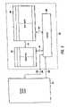
- FIG. 1shows a schematic block diagram of an architecture for a semiconductor mass storage according to the present invention.
- FIG. 2shows an alternative embodiment to the physical block address 102 of the RAM storage of FIG. 1 .
- FIG. 3shows a block diagram of a system incorporating the mass storage device of the present invention.
- FIGS. 4 through 8show the status of several of the flags and information for achieving the advantages of the present invention.
- FIG. 9shows a flow chart block diagram of the first algorithm according to the present invention.
- FIG. 1shows an architecture for implementation of a solid state storage media according to the present invention.
- the storage mediais for use with a host or other external digital system.
- the mass storageis partitioned into two portions, a volatile RAM array 100 and a nonvolatile array 104 .
- all of the nonvolatile memory storageis FLASH.
- the FLASHmay be replaced by EEPROM.
- the RAMcan be of any convenient type.
- the memory storage 104is arranged into N blocks of data from zero through N ⁇ 1.
- Each of the blocks of datais M Bytes long.
- each data blockis 512 Bytes long to correspond with a sector length in a commercially available hard disk drive plus the extra numbers of bytes to store the flags and logical block address information and the associated ECC.
- the memory 104can contain as much memory storage as a user desires.
- An example of a mass storage devicemight include 100 M Byte of addressable storage.
- Each RAM location 102is uniquely addressable by controller using an appropriate one of the logical block addresses provided by the host system or the actual physical address of the nonvolatile media.
- the RAM location 102contains the physical block address of the data associated with the logical block address and the flags associated with a physical block address on the nonvolatile media.
- the physical block addresscan be split into two fields as shown in FIG. 2 . These fields can be used for cluster addresses of a group of data blocks. The first such field 290 is used to select a cluster address and the second such field 292 can be used to select the start address of the logical block address associated with this cluster.
- a collection of information flagsis also stored for each nonvolatile memory location 106 . These flags include an old/new flag 110 , a used/free flag 112 , a defect flag, 114 , and a single/sector flag 116 . Additionally, there is also a data store 122 .
- a controllerdetermines the first available physical block for storing the data.
- the RAM location 102 corresponding to the logical block address selected by the hostis written with the physical block address where the data is actually stored within the nonvolatile memory array in 104 ( FIG. 1 ).
- the documentwill be stored in the mass storage system.
- the host systemwill assign it a logical block address.
- the mass storage system of the present inventionwill select a physical address of an unused block or blocks in the mass storage for storing the document.
- the address of the physical block addresswill be stored into the RAM location 102 corresponding to the logical block address.
- the system of the present inventionalso Sets the used/free flag 112 in 104 and 293 to indicate that this block location is used.
- One used/free flag 112is provided for each entry of the nonvolatile array 104 .
- the system of the present inventionprovides means for locating a block having its used/free flag 112 in 100 unset (not programmed) which indicates that the associated block is erased.
- the systemsets the used/free flag for the new block 112 of 106 and 293 of 100 and then stores the modified document in that new physical block location 106 in the nonvolatile array 104 .
- the address of the new physical block locationis also stored into the RAM location 102 corresponding the logical block address, thereby writing over the previous physical block location in 102 .
- the systemsets the old/new flag 110 of the previous version of the document indicating that this is an old unneeded version of the document in 110 of 104 and 293 of 100 In this way, the system of the present invention avoids the overhead of an erase cycle which is required in the erase-before-write of conventional systems to store a modified version of a previous document.
- the logical block address with the active physical block address in the mediais also stored as a shadow memory 108 in the nonvolatile array 104 . It will be understood the shadow information will be stored into the appropriate RAM locations 102 by the controller. During power up sequence, the RAM locations in 100 are appropriately updated from every physical locations in 104 , by reading the information 106 of 104 . The logical address 108 of 106 is used to address the RAM location of 100 to update the actual physical block address associated with the given logical block address.
- the flags 110 , 112 , 114 , and 116are updated in 293 of 102 with the physical block address of 106 in 100 . It will be apparent to one of ordinary skill in the art that the flags can be stored in either the appropriate nonvolatile memory location 106 or in both the nonvolatile memory location and also in the RAM location 102 associated with the physical block address.
- the controllerwill first reads the Flags 110 , 112 , 114 , and 116 portion of the nonvolatile memory 104 and updates the flags portion 293 in the volatile memory 100 . Then it reads the logical block address 108 of every physical block address of the nonvolatile media 104 and by tracking the flags of the given physical block address in the volatile memory 100 , and the read logical block address of the physical block address in the nonvolatile memory 104 , it can update the most recent physical block address assigned to the read logical block address in the volatile memory 100 .
- FIG. 3shows a block diagram of a system incorporating the mass storage device of the present invention.
- An external digital system 300such as a host computer, personal computer and the like is coupled to the mass storage device 302 of the present invention.
- a logical block addressis coupled via an address bus 306 to the volatile RAM array 100 and to a controller circuit 30 t Control signals are also coupled to the controller 304 via a control bus 308 .
- the volatile RAM array 100is coupled via data paths 140 for providing the physical block address to the nonvolatile RAM array 104 .
- the controller 304is coupled to control both the volatile RAM 100 , the nonvolatile array 104 , and for the generation of all flags.
- FIGS. 4 through 8A simplified example, showing the operation of the write operation according to the present invention is shown in FIGS. 4 through 8 . Not all the information flags are shown to avoid obscuring these features of the invention in excessive detail.
- the data entriesare shown using decimal numbers to further simplify the understanding of the invention. It will be apparent to one of ordinary skill in the art that in a preferred embodiment binary counting will be used.
- FIG. 4shows an eleven entry mass storage device according to the present invention. There is no valid nor usable data stored in the mass storage device of FIG. 4 . Accordingly, all the physical block addresses are empty. The data stored in the nonvolatile mass storage location ‘ 6 ’ is filled and old. Additionally, location ‘ 9 ’ is defective and cannot be used.
- the hostdirects the mass storage device of the example to write data pursuant to the logical block address ‘ 3 ’ and then to ‘ 4 ’
- the mass storage devicewill first write the data associated with the logical block address ‘ 3 ’.
- the devicedetermines which is the first unused location in the nonvolatile memory. In this example, the first empty location is location ‘ 0 ’. Accordingly, FIG. 5 shows that for the logical block address ‘ 3 ’, the corresponding physical block address ‘ 0 ’ is stored and the used flag is set in physical block address ‘ 0 ’. The next empty location is location ‘ 1 ’.
- FIG. 6shows that for the logical block address ‘ 4 ’, the corresponding physical block address ‘ 1 ’ is stored and the used flag is set in physical block address ‘ 1 ’.
- FIG. 7shows that the old flag in location ‘ 0 ’ is set to indicate that this data is no longer usable, the used flag is set in location ‘ 2 ’ and the physical block address in location ‘ 3 ’ is changed to ‘ 2 .
- FIG. 8shows that the old flag in location ‘ 1 ’ is set to indicate that this data is no longer usable, the used flag is set in location ‘ 3 ’ and the physical block address in location ‘ 4 ’ is changed to ‘ 3 ’. (Recall that there is generally no relation between the physical block address and the data stored in the same location.)
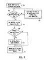
- FIG. 9shows algorithm 1 according to the present invention.
- the system of the present inventionreceives an instruction to program data into the mass storage (step 200 ), then the system attempts to locate a free block (step 202 ), i.e., a block having an unset (not programmed) used/free flag. If successful, the system sets the used/free flag for that block and programs the data into that block (step 206 ).
- the systemIf on the other hand, the system is unable to locate a block having an unset used/free flag, the system erases the flags (used/free and old/new) and data for all blocks having a set old/new flag and unset defect flag (step 204 ) and then searches for a block having an unset used/free flag (step 202 ). Such a block has just been formed by step 204 . The system then sets the used/flag for that block and programs the data file into that block (step 206 ).
- the systemdetermines whether the data file supersedes a previous data file (step 208 ). If so, the system sets the old/new flag associated with the superseded block (step 210 ). If on the other hand, the data file to be stored is a newly created data file, the step of setting the old/new flag (step 210 ) is skipped because there is no superseded block. Lastly, the map for correlating the logical address 108 to the physical address 130 is updated (step 2 t 2 i
- the programming of the flash memoryfollows the procedure commonly understood by those of ordinary skill in the art.
- the program impulsesare appropriately applied to the bits to be programmed and then compared to the data being programmed to ensure that proper programming has occurred.
- a defect flag 114(in FIG. 1 ) is set which prevent that block from being used again.
Landscapes
- Engineering & Computer Science (AREA)
- Theoretical Computer Science (AREA)
- Physics & Mathematics (AREA)
- General Engineering & Computer Science (AREA)
- General Physics & Mathematics (AREA)
- Human Computer Interaction (AREA)
- Techniques For Improving Reliability Of Storages (AREA)
- Read Only Memory (AREA)
Abstract
Description
Claims (22)
Priority Applications (3)
| Application Number | Priority Date | Filing Date | Title |
|---|---|---|---|
| US11/165,864US7523249B1 (en) | 1995-07-31 | 2005-06-24 | Direct logical block addressing flash memory mass storage architecture |
| US12/426,662US7774576B2 (en) | 1995-07-31 | 2009-04-20 | Direct logical block addressing flash memory mass storage architecture |
| US12/844,354US8032694B2 (en) | 1995-07-31 | 2010-07-27 | Direct logical block addressing flash memory mass storage architecture |
Applications Claiming Priority (6)
| Application Number | Priority Date | Filing Date | Title |
|---|---|---|---|
| US08/509,706US5845313A (en) | 1995-07-31 | 1995-07-31 | Direct logical block addressing flash memory mass storage architecture |
| US09/087,720US5924113A (en) | 1995-07-31 | 1998-05-29 | Direct logical block addressing flash memory mass storage architecture |
| US09/311,045US6115785A (en) | 1995-07-31 | 1999-05-13 | Direct logical block addressing flash memory mass storage architecture |
| US09/521,420US6230234B1 (en) | 1995-07-31 | 2000-03-08 | Direct logical block addressing flash memory mass storage architecture |
| US09/850,790US6912618B2 (en) | 1995-07-31 | 2001-05-07 | Direct logical block addressing flash memory mass storage architecture |
| US11/165,864US7523249B1 (en) | 1995-07-31 | 2005-06-24 | Direct logical block addressing flash memory mass storage architecture |
Related Parent Applications (1)
| Application Number | Title | Priority Date | Filing Date |
|---|---|---|---|
| US09/850,790ContinuationUS6912618B2 (en) | 1995-07-31 | 2001-05-07 | Direct logical block addressing flash memory mass storage architecture |
Related Child Applications (1)
| Application Number | Title | Priority Date | Filing Date |
|---|---|---|---|
| US12/426,662ContinuationUS7774576B2 (en) | 1995-07-31 | 2009-04-20 | Direct logical block addressing flash memory mass storage architecture |
Publications (1)
| Publication Number | Publication Date |
|---|---|
| US7523249B1true US7523249B1 (en) | 2009-04-21 |
Family
ID=24027781
Family Applications (8)
| Application Number | Title | Priority Date | Filing Date |
|---|---|---|---|
| US08/509,706Expired - LifetimeUS5845313A (en) | 1995-07-31 | 1995-07-31 | Direct logical block addressing flash memory mass storage architecture |
| US09/087,720Expired - LifetimeUS5924113A (en) | 1995-07-31 | 1998-05-29 | Direct logical block addressing flash memory mass storage architecture |
| US09/311,045Expired - LifetimeUS6115785A (en) | 1995-07-31 | 1999-05-13 | Direct logical block addressing flash memory mass storage architecture |
| US09/521,420Expired - LifetimeUS6230234B1 (en) | 1995-07-31 | 2000-03-08 | Direct logical block addressing flash memory mass storage architecture |
| US09/850,790Expired - Fee RelatedUS6912618B2 (en) | 1995-07-31 | 2001-05-07 | Direct logical block addressing flash memory mass storage architecture |
| US11/165,864Expired - Fee RelatedUS7523249B1 (en) | 1995-07-31 | 2005-06-24 | Direct logical block addressing flash memory mass storage architecture |
| US12/426,662Expired - Fee RelatedUS7774576B2 (en) | 1995-07-31 | 2009-04-20 | Direct logical block addressing flash memory mass storage architecture |
| US12/844,354Expired - Fee RelatedUS8032694B2 (en) | 1995-07-31 | 2010-07-27 | Direct logical block addressing flash memory mass storage architecture |
Family Applications Before (5)
| Application Number | Title | Priority Date | Filing Date |
|---|---|---|---|
| US08/509,706Expired - LifetimeUS5845313A (en) | 1995-07-31 | 1995-07-31 | Direct logical block addressing flash memory mass storage architecture |
| US09/087,720Expired - LifetimeUS5924113A (en) | 1995-07-31 | 1998-05-29 | Direct logical block addressing flash memory mass storage architecture |
| US09/311,045Expired - LifetimeUS6115785A (en) | 1995-07-31 | 1999-05-13 | Direct logical block addressing flash memory mass storage architecture |
| US09/521,420Expired - LifetimeUS6230234B1 (en) | 1995-07-31 | 2000-03-08 | Direct logical block addressing flash memory mass storage architecture |
| US09/850,790Expired - Fee RelatedUS6912618B2 (en) | 1995-07-31 | 2001-05-07 | Direct logical block addressing flash memory mass storage architecture |
Family Applications After (2)
| Application Number | Title | Priority Date | Filing Date |
|---|---|---|---|
| US12/426,662Expired - Fee RelatedUS7774576B2 (en) | 1995-07-31 | 2009-04-20 | Direct logical block addressing flash memory mass storage architecture |
| US12/844,354Expired - Fee RelatedUS8032694B2 (en) | 1995-07-31 | 2010-07-27 | Direct logical block addressing flash memory mass storage architecture |
Country Status (1)
| Country | Link |
|---|---|
| US (8) | US5845313A (en) |
Cited By (22)
| Publication number | Priority date | Publication date | Assignee | Title |
|---|---|---|---|---|
| US20080162796A1 (en)* | 2006-12-28 | 2008-07-03 | Genesys Logic, Inc. | Method for performing static wear leveling on flash memory |
| US20090182962A1 (en)* | 2008-01-16 | 2009-07-16 | Apple Inc. | Memory Subsystem Hibernation |
| US20110066808A1 (en)* | 2009-09-08 | 2011-03-17 | Fusion-Io, Inc. | Apparatus, System, and Method for Caching Data on a Solid-State Storage Device |
| US8189407B2 (en) | 2006-12-06 | 2012-05-29 | Fusion-Io, Inc. | Apparatus, system, and method for biasing data in a solid-state storage device |
| US8316277B2 (en) | 2007-12-06 | 2012-11-20 | Fusion-Io, Inc. | Apparatus, system, and method for ensuring data validity in a data storage process |
| US8443134B2 (en) | 2006-12-06 | 2013-05-14 | Fusion-Io, Inc. | Apparatus, system, and method for graceful cache device degradation |
| US8489817B2 (en) | 2007-12-06 | 2013-07-16 | Fusion-Io, Inc. | Apparatus, system, and method for caching data |
| US8706968B2 (en) | 2007-12-06 | 2014-04-22 | Fusion-Io, Inc. | Apparatus, system, and method for redundant write caching |
| US8782344B2 (en) | 2012-01-12 | 2014-07-15 | Fusion-Io, Inc. | Systems and methods for managing cache admission |
| US8825937B2 (en) | 2011-02-25 | 2014-09-02 | Fusion-Io, Inc. | Writing cached data forward on read |
| US8966184B2 (en) | 2011-01-31 | 2015-02-24 | Intelligent Intellectual Property Holdings 2, LLC. | Apparatus, system, and method for managing eviction of data |
| US9104599B2 (en) | 2007-12-06 | 2015-08-11 | Intelligent Intellectual Property Holdings 2 Llc | Apparatus, system, and method for destaging cached data |
| US9116823B2 (en) | 2006-12-06 | 2015-08-25 | Intelligent Intellectual Property Holdings 2 Llc | Systems and methods for adaptive error-correction coding |
| US9170754B2 (en) | 2007-12-06 | 2015-10-27 | Intelligent Intellectual Property Holdings 2 Llc | Apparatus, system, and method for coordinating storage requests in a multi-processor/multi-thread environment |
| US9251086B2 (en) | 2012-01-24 | 2016-02-02 | SanDisk Technologies, Inc. | Apparatus, system, and method for managing a cache |
| US9251052B2 (en) | 2012-01-12 | 2016-02-02 | Intelligent Intellectual Property Holdings 2 Llc | Systems and methods for profiling a non-volatile cache having a logical-to-physical translation layer |
| US9466383B2 (en) | 2013-12-30 | 2016-10-11 | Sandisk Technologies Llc | Non-volatile memory and method with adaptive logical groups |
| US9495241B2 (en) | 2006-12-06 | 2016-11-15 | Longitude Enterprise Flash S.A.R.L. | Systems and methods for adaptive data storage |
| US9519540B2 (en) | 2007-12-06 | 2016-12-13 | Sandisk Technologies Llc | Apparatus, system, and method for destaging cached data |
| US9767032B2 (en) | 2012-01-12 | 2017-09-19 | Sandisk Technologies Llc | Systems and methods for cache endurance |
| US10019353B2 (en) | 2012-03-02 | 2018-07-10 | Longitude Enterprise Flash S.A.R.L. | Systems and methods for referencing data on a storage medium |
| US10102117B2 (en) | 2012-01-12 | 2018-10-16 | Sandisk Technologies Llc | Systems and methods for cache and storage device coordination |
Families Citing this family (204)
| Publication number | Priority date | Publication date | Assignee | Title |
|---|---|---|---|---|
| US5430859A (en)* | 1991-07-26 | 1995-07-04 | Sundisk Corporation | Solid state memory system including plural memory chips and a serialized bus |
| JP3782840B2 (en) | 1995-07-14 | 2006-06-07 | 株式会社ルネサステクノロジ | External storage device and memory access control method thereof |
| US6728851B1 (en) | 1995-07-31 | 2004-04-27 | Lexar Media, Inc. | Increasing the memory performance of flash memory devices by writing sectors simultaneously to multiple flash memory devices |
| US5845313A (en) | 1995-07-31 | 1998-12-01 | Lexar | Direct logical block addressing flash memory mass storage architecture |
| US8171203B2 (en) | 1995-07-31 | 2012-05-01 | Micron Technology, Inc. | Faster write operations to nonvolatile memory using FSInfo sector manipulation |
| US6801979B1 (en) | 1995-07-31 | 2004-10-05 | Lexar Media, Inc. | Method and apparatus for memory control circuit |
| US6081878A (en) | 1997-03-31 | 2000-06-27 | Lexar Media, Inc. | Increasing the memory performance of flash memory devices by writing sectors simultaneously to multiple flash memory devices |
| US6757800B1 (en) | 1995-07-31 | 2004-06-29 | Lexar Media, Inc. | Increasing the memory performance of flash memory devices by writing sectors simultaneously to multiple flash memory devices |
| US6978342B1 (en) | 1995-07-31 | 2005-12-20 | Lexar Media, Inc. | Moving sectors within a block of information in a flash memory mass storage architecture |
| US6125435A (en)* | 1995-09-13 | 2000-09-26 | Lexar Media, Inc. | Alignment of cluster address to block addresses within a semiconductor non-volatile mass storage memory |
| US6035369A (en)* | 1995-10-19 | 2000-03-07 | Rambus Inc. | Method and apparatus for providing a memory with write enable information |
| JP3614173B2 (en) | 1996-02-29 | 2005-01-26 | 株式会社ルネサステクノロジ | Semiconductor memory device with partially defective memory |
| US5890192A (en)* | 1996-11-05 | 1999-03-30 | Sandisk Corporation | Concurrent write of multiple chunks of data into multiple subarrays of flash EEPROM |
| US5953737A (en)* | 1997-03-31 | 1999-09-14 | Lexar Media, Inc. | Method and apparatus for performing erase operations transparent to a solid state storage system |
| US6411546B1 (en) | 1997-03-31 | 2002-06-25 | Lexar Media, Inc. | Nonvolatile memory using flexible erasing methods and method and system for using same |
| KR100251636B1 (en)* | 1997-04-10 | 2000-05-01 | 윤종용 | Memory device for connecting in a accordance with scsi |
| JP3718578B2 (en)* | 1997-06-25 | 2005-11-24 | ソニー株式会社 | Memory management method and memory management device |
| JPH11110267A (en)* | 1997-10-02 | 1999-04-23 | Oki Electric Ind Co Ltd | Device and method for data storing and storage medium |
| JP3714969B2 (en) | 1998-03-02 | 2005-11-09 | レクサー・メディア・インコーポレイテッド | Flash memory card with improved operating mode detection and user-friendly interfacing system |
| WO2000013089A1 (en)* | 1998-08-31 | 2000-03-09 | Sony Corporation | Storage, processor, and processing method |
| CN1126037C (en) | 1998-09-04 | 2003-10-29 | 奥托·穆勒 | Method for access control of memory with limited deletion frequency |
| US6901457B1 (en) | 1998-11-04 | 2005-05-31 | Sandisk Corporation | Multiple mode communications system |
| AU1729100A (en) | 1998-11-17 | 2000-06-05 | Lexar Media, Inc. | Method and apparatus for memory control circuit |
| FR2787601A1 (en)* | 1998-12-22 | 2000-06-23 | Gemplus Card Int | Memory system with anti-wear memory management and method of managing an anti-wear memory so as to increase duration life of memory |
| US6345349B1 (en)* | 1998-12-30 | 2002-02-05 | Intel Corporation | Combined memory and mass storage device |
| JP2000227871A (en)* | 1999-02-05 | 2000-08-15 | Seiko Epson Corp | Nonvolatile storage device, control method therefor, and information recording medium |
| US6148354A (en)* | 1999-04-05 | 2000-11-14 | M-Systems Flash Disk Pioneers Ltd. | Architecture for a universal serial bus-based PC flash disk |
| US7102671B1 (en) | 2000-02-08 | 2006-09-05 | Lexar Media, Inc. | Enhanced compact flash memory card |
| US6606628B1 (en)* | 2000-02-14 | 2003-08-12 | Cisco Technology, Inc. | File system for nonvolatile memory |
| US6426893B1 (en) | 2000-02-17 | 2002-07-30 | Sandisk Corporation | Flash eeprom system with simultaneous multiple data sector programming and storage of physical block characteristics in other designated blocks |
| EP1130516A1 (en)* | 2000-03-01 | 2001-09-05 | Hewlett-Packard Company, A Delaware Corporation | Address mapping in solid state storage device |
| US7167944B1 (en) | 2000-07-21 | 2007-01-23 | Lexar Media, Inc. | Block management for mass storage |
| US7155559B1 (en) | 2000-08-25 | 2006-12-26 | Lexar Media, Inc. | Flash memory architecture with separate storage of overhead and user data |
| US6772274B1 (en) | 2000-09-13 | 2004-08-03 | Lexar Media, Inc. | Flash memory system and method implementing LBA to PBA correlation within flash memory array |
| US7113432B2 (en) | 2000-09-14 | 2006-09-26 | Sandisk Corporation | Compressed event counting technique and application to a flash memory system |
| US6763424B2 (en) | 2001-01-19 | 2004-07-13 | Sandisk Corporation | Partial block data programming and reading operations in a non-volatile memory |
| US20020108018A1 (en)* | 2001-02-05 | 2002-08-08 | Han-Ping Chen | Memory module control and status |
| KR100389867B1 (en)* | 2001-06-04 | 2003-07-04 | 삼성전자주식회사 | Flash memory management method |
| US7275135B2 (en)* | 2001-08-31 | 2007-09-25 | Intel Corporation | Hardware updated metadata for non-volatile mass storage cache |
| GB0123419D0 (en) | 2001-09-28 | 2001-11-21 | Memquest Ltd | Data handling system |
| GB0123415D0 (en) | 2001-09-28 | 2001-11-21 | Memquest Ltd | Method of writing data to non-volatile memory |
| GB0123416D0 (en) | 2001-09-28 | 2001-11-21 | Memquest Ltd | Non-volatile memory control |
| GB0123410D0 (en) | 2001-09-28 | 2001-11-21 | Memquest Ltd | Memory system for data storage and retrieval |
| GB0123421D0 (en) | 2001-09-28 | 2001-11-21 | Memquest Ltd | Power management system |
| GB0123417D0 (en) | 2001-09-28 | 2001-11-21 | Memquest Ltd | Improved data processing |
| US20030074524A1 (en)* | 2001-10-16 | 2003-04-17 | Intel Corporation | Mass storage caching processes for power reduction |
| US6977847B2 (en)* | 2001-11-23 | 2005-12-20 | M-Systems Flash Disk Pioneers Ltd. | Detecting partially erased units in flash devices |
| JP3967121B2 (en)* | 2001-12-11 | 2007-08-29 | 株式会社ルネサステクノロジ | File system, file system control method, and program for controlling file system |
| US6950918B1 (en) | 2002-01-18 | 2005-09-27 | Lexar Media, Inc. | File management of one-time-programmable nonvolatile memory devices |
| US6957295B1 (en) | 2002-01-18 | 2005-10-18 | Lexar Media, Inc. | File management of one-time-programmable nonvolatile memory devices |
| DE60332091D1 (en)* | 2002-01-31 | 2010-05-27 | Panasonic Corp | INFORMATION PROCESSING DEVICE, MEMORY MANAGEMENT DEVICE, MEMORY MANAGEMENT PROCESS AND INFORMATION PROCESSING METHOD |
| US6839826B2 (en) | 2002-02-06 | 2005-01-04 | Sandisk Corporation | Memory device with pointer structure to map logical to physical addresses |
| AU2003211154A1 (en) | 2002-02-22 | 2003-09-09 | Lexar Media, Inc. | Removable memory media with integral indicator light |
| US7231643B1 (en) | 2002-02-22 | 2007-06-12 | Lexar Media, Inc. | Image rescue system including direct communication between an application program and a device driver |
| JP2003256228A (en)* | 2002-02-28 | 2003-09-10 | Denso Corp | Program rewriting device |
| WO2004031961A1 (en)* | 2002-09-30 | 2004-04-15 | Insignia Solutions Plc | Efficient system and method for updating a memory device |
| EP1548602B1 (en)* | 2002-10-02 | 2008-03-12 | Matsushita Electric Industrial Co., Ltd. | Non-volatile storage device control method |
| US6985992B1 (en) | 2002-10-28 | 2006-01-10 | Sandisk Corporation | Wear-leveling in non-volatile storage systems |
| US7035967B2 (en)* | 2002-10-28 | 2006-04-25 | Sandisk Corporation | Maintaining an average erase count in a non-volatile storage system |
| US7039788B1 (en) | 2002-10-28 | 2006-05-02 | Sandisk Corporation | Method and apparatus for splitting a logical block |
| US7181611B2 (en)* | 2002-10-28 | 2007-02-20 | Sandisk Corporation | Power management block for use in a non-volatile memory system |
| US7103732B1 (en) | 2002-10-28 | 2006-09-05 | Sandisk Corporation | Method and apparatus for managing an erase count block |
| US7096313B1 (en) | 2002-10-28 | 2006-08-22 | Sandisk Corporation | Tracking the least frequently erased blocks in non-volatile memory systems |
| US6831865B2 (en)* | 2002-10-28 | 2004-12-14 | Sandisk Corporation | Maintaining erase counts in non-volatile storage systems |
| US7171536B2 (en)* | 2002-10-28 | 2007-01-30 | Sandisk Corporation | Unusable block management within a non-volatile memory system |
| US7254668B1 (en) | 2002-10-28 | 2007-08-07 | Sandisk Corporation | Method and apparatus for grouping pages within a block |
| US6973531B1 (en) | 2002-10-28 | 2005-12-06 | Sandisk Corporation | Tracking the most frequently erased blocks in non-volatile memory systems |
| US8412879B2 (en)* | 2002-10-28 | 2013-04-02 | Sandisk Technologies Inc. | Hybrid implementation for error correction codes within a non-volatile memory system |
| US20040083334A1 (en)* | 2002-10-28 | 2004-04-29 | Sandisk Corporation | Method and apparatus for managing the integrity of data in non-volatile memory system |
| US7174440B2 (en)* | 2002-10-28 | 2007-02-06 | Sandisk Corporation | Method and apparatus for performing block caching in a non-volatile memory system |
| US7526599B2 (en)* | 2002-10-28 | 2009-04-28 | Sandisk Corporation | Method and apparatus for effectively enabling an out of sequence write process within a non-volatile memory system |
| US7234036B1 (en) | 2002-10-28 | 2007-06-19 | Sandisk Corporation | Method and apparatus for resolving physical blocks associated with a common logical block |
| US6973519B1 (en) | 2003-06-03 | 2005-12-06 | Lexar Media, Inc. | Card identification compatibility |
| US7559004B1 (en) | 2003-10-01 | 2009-07-07 | Sandisk Corporation | Dynamic redundant area configuration in a non-volatile memory system |
| US7188228B1 (en) | 2003-10-01 | 2007-03-06 | Sandisk Corporation | Hybrid mapping implementation within a non-volatile memory system |
| US7032087B1 (en) | 2003-10-28 | 2006-04-18 | Sandisk Corporation | Erase count differential table within a non-volatile memory system |
| US8706990B2 (en) | 2003-10-28 | 2014-04-22 | Sandisk Technologies Inc. | Adaptive internal table backup for non-volatile memory system |
| US7089349B2 (en)* | 2003-10-28 | 2006-08-08 | Sandisk Corporation | Internal maintenance schedule request for non-volatile memory system |
| US7275686B2 (en) | 2003-12-17 | 2007-10-02 | Lexar Media, Inc. | Electronic equipment point-of-sale activation to avoid theft |
| JP2005190288A (en)* | 2003-12-26 | 2005-07-14 | Tdk Corp | Memory controller, flash memory system therewith, and method for controlling flash memory |
| US8504798B2 (en)* | 2003-12-30 | 2013-08-06 | Sandisk Technologies Inc. | Management of non-volatile memory systems having large erase blocks |
| US7631138B2 (en) | 2003-12-30 | 2009-12-08 | Sandisk Corporation | Adaptive mode switching of flash memory address mapping based on host usage characteristics |
| US7725628B1 (en) | 2004-04-20 | 2010-05-25 | Lexar Media, Inc. | Direct secondary device interface by a host |
| US7370166B1 (en) | 2004-04-30 | 2008-05-06 | Lexar Media, Inc. | Secure portable storage device |
| US7240065B2 (en)* | 2004-05-27 | 2007-07-03 | Oracle International Corporation | Providing mappings between logical time values and real time values |
| JP4253272B2 (en) | 2004-05-27 | 2009-04-08 | 株式会社東芝 | Memory card, semiconductor device, and control method of semiconductor memory |
| US7251660B2 (en) | 2004-06-10 | 2007-07-31 | Oracle International Corporation | Providing mappings between logical time values and real time values in a multinode system |
| US7492953B2 (en)* | 2004-06-17 | 2009-02-17 | Smith Micro Software, Inc. | Efficient method and system for reducing update requirements for a compressed binary image |
| US7594063B1 (en) | 2004-08-27 | 2009-09-22 | Lexar Media, Inc. | Storage capacity status |
| US7464306B1 (en) | 2004-08-27 | 2008-12-09 | Lexar Media, Inc. | Status of overall health of nonvolatile memory |
| KR100725390B1 (en)* | 2005-01-06 | 2007-06-07 | 삼성전자주식회사 | Apparatus and method for storing data in nonvolatile cache in consideration of modification frequency |
| JP2006227818A (en)* | 2005-02-16 | 2006-08-31 | Fujitsu Ltd | IDENTIFICATION INFORMATION DIAGNOSIS METHOD AND INPUT / OUTPUT DEVICE |
| US20070006000A1 (en)* | 2005-06-30 | 2007-01-04 | Sandeep Jain | Using fine-grained power management of physical system memory to improve system sleep |
| US8561049B2 (en)* | 2005-08-23 | 2013-10-15 | Red Bend Ltd. | Method and system for updating content stored in a storage device |
| US7652922B2 (en)* | 2005-09-30 | 2010-01-26 | Mosaid Technologies Incorporated | Multiple independent serial link memory |
| KR101293365B1 (en) | 2005-09-30 | 2013-08-05 | 모사이드 테크놀로지스 인코퍼레이티드 | Memory with output control |
| US11948629B2 (en) | 2005-09-30 | 2024-04-02 | Mosaid Technologies Incorporated | Non-volatile memory device with concurrent bank operations |
| US20070083697A1 (en)* | 2005-10-07 | 2007-04-12 | Microsoft Corporation | Flash memory management |
| US7631162B2 (en) | 2005-10-27 | 2009-12-08 | Sandisck Corporation | Non-volatile memory with adaptive handling of data writes |
| US7509471B2 (en)* | 2005-10-27 | 2009-03-24 | Sandisk Corporation | Methods for adaptively handling data writes in non-volatile memories |
| WO2007081598A2 (en)* | 2005-10-27 | 2007-07-19 | Sandisk Corporation | Adaptive handling data writes in non-volatile memories |
| US7831783B2 (en)* | 2005-12-22 | 2010-11-09 | Honeywell International Inc. | Effective wear-leveling and concurrent reclamation method for embedded linear flash file systems |
| US7464240B2 (en)* | 2006-05-23 | 2008-12-09 | Data Ram, Inc. | Hybrid solid state disk drive with controller |
| US7461229B2 (en)* | 2006-05-23 | 2008-12-02 | Dataram, Inc. | Software program for managing and protecting data written to a hybrid solid-state disk drive |
| US7783956B2 (en)* | 2006-07-12 | 2010-08-24 | Cronera Systems Incorporated | Data recorder |
| EP2045722A4 (en)* | 2006-07-20 | 2010-07-21 | Nec Corp | Memory access control device, memory access control method, data storage method, and memory access control program |
| US20080071968A1 (en)* | 2006-09-18 | 2008-03-20 | Phison Electronics Corp. | Method of managing blocks fo flash memory suitable for flexible correspondence between logic block and physical block |
| US8935302B2 (en)* | 2006-12-06 | 2015-01-13 | Intelligent Intellectual Property Holdings 2 Llc | Apparatus, system, and method for data block usage information synchronization for a non-volatile storage volume |
| WO2008087634A1 (en)* | 2007-01-18 | 2008-07-24 | Sandisk Il Ltd. | A method and system for facilitating fast wake-up of a flash memory system |
| US7721040B2 (en)* | 2007-01-18 | 2010-05-18 | Sandisk Il Ltd. | Method and system for facilitating fast wake-up of a flash memory system |
| US7814360B2 (en)* | 2007-01-25 | 2010-10-12 | Oralce International Corporation | Synchronizing cluster time to a master node with a faster clock |
| US20080189473A1 (en)* | 2007-02-07 | 2008-08-07 | Micron Technology, Inc | Mlc selected multi-program for system management |
| JP4874844B2 (en)* | 2007-03-26 | 2012-02-15 | 株式会社東芝 | Information recording apparatus and control method thereof |
| US8239639B2 (en)* | 2007-06-08 | 2012-08-07 | Sandisk Technologies Inc. | Method and apparatus for providing data type and host file information to a mass storage system |
| US20080307156A1 (en)* | 2007-06-08 | 2008-12-11 | Sinclair Alan W | System For Interfacing A Host Operating Through A Logical Address Space With A Direct File Storage Medium |
| US8713283B2 (en)* | 2007-06-08 | 2014-04-29 | Sandisk Technologies Inc. | Method of interfacing a host operating through a logical address space with a direct file storage medium |
| US8307180B2 (en) | 2008-02-28 | 2012-11-06 | Nokia Corporation | Extended utilization area for a memory device |
| JP5218228B2 (en)* | 2008-04-23 | 2013-06-26 | 新東工業株式会社 | Conveying device and blasting device |
| US8285919B2 (en)* | 2008-05-27 | 2012-10-09 | Initio Corporation | SSD with improved bad block management |
| WO2009149059A1 (en)* | 2008-06-04 | 2009-12-10 | Initio Corporation | Ssd with a controller accelerator |
| US8843691B2 (en)* | 2008-06-25 | 2014-09-23 | Stec, Inc. | Prioritized erasure of data blocks in a flash storage device |
| US8139390B2 (en)* | 2008-07-08 | 2012-03-20 | Mosaid Technologies Incorporated | Mixed data rates in memory devices and systems |
| US20100082903A1 (en)* | 2008-09-30 | 2010-04-01 | Kabushiki Kaisha Toshiba | Non-volatile semiconductor memory drive, information processing apparatus and data access control method of the non-volatile semiconductor memory drive |
| US9128821B2 (en) | 2008-10-10 | 2015-09-08 | Seagate Technology Llc | Data updating in non-volatile memory |
| US8169856B2 (en)* | 2008-10-24 | 2012-05-01 | Oracle International Corporation | Time synchronization in cluster systems |
| US9020993B2 (en) | 2008-12-16 | 2015-04-28 | Sandisk Il Ltd. | Download management of discardable files |
| US8849856B2 (en)* | 2008-12-16 | 2014-09-30 | Sandisk Il Ltd. | Discardable files |
| US8205060B2 (en)* | 2008-12-16 | 2012-06-19 | Sandisk Il Ltd. | Discardable files |
| US8375192B2 (en)* | 2008-12-16 | 2013-02-12 | Sandisk Il Ltd. | Discardable files |
| US9104686B2 (en) | 2008-12-16 | 2015-08-11 | Sandisk Technologies Inc. | System and method for host management of discardable objects |
| US20100153474A1 (en)* | 2008-12-16 | 2010-06-17 | Sandisk Il Ltd. | Discardable files |
| US9015209B2 (en) | 2008-12-16 | 2015-04-21 | Sandisk Il Ltd. | Download management of discardable files |
| US8180995B2 (en) | 2009-01-21 | 2012-05-15 | Micron Technology, Inc. | Logical address offset in response to detecting a memory formatting operation |
| US20100235329A1 (en)* | 2009-03-10 | 2010-09-16 | Sandisk Il Ltd. | System and method of embedding second content in first content |
| TWI457940B (en)* | 2009-05-15 | 2014-10-21 | Macronix Int Co Ltd | Byte-access in block-based flash memory |
| US8874824B2 (en) | 2009-06-04 | 2014-10-28 | Memory Technologies, LLC | Apparatus and method to share host system RAM with mass storage memory RAM |
| US9342445B2 (en) | 2009-07-23 | 2016-05-17 | Hgst Technologies Santa Ana, Inc. | System and method for performing a direct memory access at a predetermined address in a flash storage |
| KR101769883B1 (en) | 2009-09-09 | 2017-08-21 | 샌디스크 테크놀로지스 엘엘씨 | Apparatus, system, and method for allocating storage |
| US9122579B2 (en) | 2010-01-06 | 2015-09-01 | Intelligent Intellectual Property Holdings 2 Llc | Apparatus, system, and method for a storage layer |
| JP2011095916A (en)* | 2009-10-28 | 2011-05-12 | Canon Inc | Electronic apparatus |
| US9110594B2 (en)* | 2009-11-04 | 2015-08-18 | Seagate Technology Llc | File management system for devices containing solid-state media |
| US8443167B1 (en) | 2009-12-16 | 2013-05-14 | Western Digital Technologies, Inc. | Data storage device employing a run-length mapping table and a single address mapping table |
| WO2011096046A1 (en)* | 2010-02-02 | 2011-08-11 | 株式会社 東芝 | Communication device having storage function |
| US8194340B1 (en) | 2010-03-18 | 2012-06-05 | Western Digital Technologies, Inc. | Disk drive framing write data with in-line mapping data during write operations |
| US8699185B1 (en) | 2012-12-10 | 2014-04-15 | Western Digital Technologies, Inc. | Disk drive defining guard bands to support zone sequentiality when butterfly writing shingled data tracks |
| US8856438B1 (en) | 2011-12-09 | 2014-10-07 | Western Digital Technologies, Inc. | Disk drive with reduced-size translation table |
| US8693133B1 (en) | 2010-03-22 | 2014-04-08 | Western Digital Technologies, Inc. | Systems and methods for improving sequential data rate performance using sorted data zones for butterfly format |
| US9330715B1 (en) | 2010-03-22 | 2016-05-03 | Western Digital Technologies, Inc. | Mapping of shingled magnetic recording media |
| US8687306B1 (en) | 2010-03-22 | 2014-04-01 | Western Digital Technologies, Inc. | Systems and methods for improving sequential data rate performance using sorted data zones |
| US20110302224A1 (en)* | 2010-06-08 | 2011-12-08 | Rahav Yairi | Data storage device with preloaded content |
| TWI457941B (en)* | 2010-06-25 | 2014-10-21 | Macronix Int Co Ltd | Method and apparatus for high-speed byte-access in block-based flash memory |
| CN102314396B (en)* | 2010-07-06 | 2014-01-29 | 旺宏电子股份有限公司 | Method and device for byte access of block-based flash memory |
| US8239619B2 (en) | 2010-07-09 | 2012-08-07 | Macronix International Co., Ltd. | Method and apparatus for high-speed byte-access in block-based flash memory |
| US8549229B2 (en) | 2010-08-19 | 2013-10-01 | Sandisk Il Ltd. | Systems and methods for managing an upload of files in a shared cache storage system |
| US8463802B2 (en) | 2010-08-19 | 2013-06-11 | Sandisk Il Ltd. | Card-based management of discardable files |
| US8667248B1 (en) | 2010-08-31 | 2014-03-04 | Western Digital Technologies, Inc. | Data storage device using metadata and mapping table to identify valid user data on non-volatile media |
| US8954664B1 (en) | 2010-10-01 | 2015-02-10 | Western Digital Technologies, Inc. | Writing metadata files on a disk |
| US8756361B1 (en) | 2010-10-01 | 2014-06-17 | Western Digital Technologies, Inc. | Disk drive modifying metadata cached in a circular buffer when a write operation is aborted |
| US20120239860A1 (en) | 2010-12-17 | 2012-09-20 | Fusion-Io, Inc. | Apparatus, system, and method for persistent data management on a non-volatile storage media |
| US8874823B2 (en) | 2011-02-15 | 2014-10-28 | Intellectual Property Holdings 2 Llc | Systems and methods for managing data input/output operations |
| US9201677B2 (en) | 2011-05-23 | 2015-12-01 | Intelligent Intellectual Property Holdings 2 Llc | Managing data input/output operations |
| US9003104B2 (en) | 2011-02-15 | 2015-04-07 | Intelligent Intellectual Property Holdings 2 Llc | Systems and methods for a file-level cache |
| US8788849B2 (en) | 2011-02-28 | 2014-07-22 | Sandisk Technologies Inc. | Method and apparatus for protecting cached streams |
| US8966191B2 (en) | 2011-03-18 | 2015-02-24 | Fusion-Io, Inc. | Logical interface for contextual storage |
| US9563555B2 (en) | 2011-03-18 | 2017-02-07 | Sandisk Technologies Llc | Systems and methods for storage allocation |
| US8793429B1 (en) | 2011-06-03 | 2014-07-29 | Western Digital Technologies, Inc. | Solid-state drive with reduced power up time |
| US20120317377A1 (en)* | 2011-06-09 | 2012-12-13 | Alexander Palay | Dual flash translation layer |
| US8954948B2 (en)* | 2011-06-17 | 2015-02-10 | Bae Systems Controls Inc. | Obsolescence tolerant flash memory architecture and physical building block (PBB) implementation |
| US8756382B1 (en) | 2011-06-30 | 2014-06-17 | Western Digital Technologies, Inc. | Method for file based shingled data storage utilizing multiple media types |
| CN102231136B (en)* | 2011-07-12 | 2014-06-11 | 晨星软件研发(深圳)有限公司 | Data storage method and device for flash memory storage equipment |
| KR20130044657A (en)* | 2011-10-24 | 2013-05-03 | 삼성전자주식회사 | File system and method for controlling the same |
| US9069657B2 (en) | 2011-12-12 | 2015-06-30 | Apple Inc. | LBA bitmap usage |
| US9213493B1 (en) | 2011-12-16 | 2015-12-15 | Western Digital Technologies, Inc. | Sorted serpentine mapping for storage drives |
| US8819367B1 (en) | 2011-12-19 | 2014-08-26 | Western Digital Technologies, Inc. | Accelerated translation power recovery |
| US8612706B1 (en) | 2011-12-21 | 2013-12-17 | Western Digital Technologies, Inc. | Metadata recovery in a disk drive |
| US9274937B2 (en) | 2011-12-22 | 2016-03-01 | Longitude Enterprise Flash S.A.R.L. | Systems, methods, and interfaces for vector input/output operations |
| US10359972B2 (en) | 2012-08-31 | 2019-07-23 | Sandisk Technologies Llc | Systems, methods, and interfaces for adaptive persistence |
| US9116812B2 (en) | 2012-01-27 | 2015-08-25 | Intelligent Intellectual Property Holdings 2 Llc | Systems and methods for a de-duplication cache |
| US9311226B2 (en) | 2012-04-20 | 2016-04-12 | Memory Technologies Llc | Managing operational state data of a memory module using host memory in association with state change |
| US9164804B2 (en)* | 2012-06-20 | 2015-10-20 | Memory Technologies Llc | Virtual memory module |
| US8910017B2 (en) | 2012-07-02 | 2014-12-09 | Sandisk Technologies Inc. | Flash memory with random partition |
| US10339056B2 (en) | 2012-07-03 | 2019-07-02 | Sandisk Technologies Llc | Systems, methods and apparatus for cache transfers |
| US9612966B2 (en) | 2012-07-03 | 2017-04-04 | Sandisk Technologies Llc | Systems, methods and apparatus for a virtual machine cache |
| US9116820B2 (en) | 2012-08-28 | 2015-08-25 | Memory Technologies Llc | Dynamic central cache memory |
| US10509776B2 (en) | 2012-09-24 | 2019-12-17 | Sandisk Technologies Llc | Time sequence data management |
| US10318495B2 (en) | 2012-09-24 | 2019-06-11 | Sandisk Technologies Llc | Snapshots for a non-volatile device |
| JP6088837B2 (en) | 2013-02-12 | 2017-03-01 | 株式会社東芝 | Storage control device, storage control method, storage system, and program |
| US9842053B2 (en) | 2013-03-15 | 2017-12-12 | Sandisk Technologies Llc | Systems and methods for persistent cache logging |
| US10558561B2 (en) | 2013-04-16 | 2020-02-11 | Sandisk Technologies Llc | Systems and methods for storage metadata management |
| US10102144B2 (en) | 2013-04-16 | 2018-10-16 | Sandisk Technologies Llc | Systems, methods and interfaces for data virtualization |
| US9842128B2 (en) | 2013-08-01 | 2017-12-12 | Sandisk Technologies Llc | Systems and methods for atomic storage operations |
| US10019320B2 (en) | 2013-10-18 | 2018-07-10 | Sandisk Technologies Llc | Systems and methods for distributed atomic storage operations |
| US10073630B2 (en) | 2013-11-08 | 2018-09-11 | Sandisk Technologies Llc | Systems and methods for log coordination |
| CN103559144A (en)* | 2013-11-12 | 2014-02-05 | 上海华兴数字科技有限公司 | Method and device for secure data storage of embedded system |
| US8953269B1 (en) | 2014-07-18 | 2015-02-10 | Western Digital Technologies, Inc. | Management of data objects in a data object zone |
| US9875055B1 (en) | 2014-08-04 | 2018-01-23 | Western Digital Technologies, Inc. | Check-pointing of metadata |
| US9946607B2 (en) | 2015-03-04 | 2018-04-17 | Sandisk Technologies Llc | Systems and methods for storage error management |
| US10078567B2 (en)* | 2016-03-18 | 2018-09-18 | Alibaba Group Holding Limited | Implementing fault tolerance in computer system memory |
| US9996273B1 (en)* | 2016-06-30 | 2018-06-12 | EMC IP Holding Company LLC | Storage system with data durability signaling for directly-addressable storage devices |
| CN106201352B (en)* | 2016-07-07 | 2019-11-29 | 广东高云半导体科技股份有限公司 | The secrecy system and decryption method of non-volatile FPGA on piece data streaming file |
| US10684947B2 (en)* | 2018-04-20 | 2020-06-16 | International Business Machines Corporation | Increasing high performance data storage utilization by reducing write operations |
| US10754785B2 (en)* | 2018-06-28 | 2020-08-25 | Intel Corporation | Checkpointing for DRAM-less SSD |
| KR20220053376A (en)* | 2020-10-22 | 2022-04-29 | 에스케이하이닉스 주식회사 | Controller and operating method thereof |
| US11765100B1 (en) | 2022-04-19 | 2023-09-19 | Bank Of America Corporation | System for intelligent capacity planning for resources with high load variance |
Citations (278)
| Publication number | Priority date | Publication date | Assignee | Title |
|---|---|---|---|---|
| US4099069A (en) | 1976-10-08 | 1978-07-04 | Westinghouse Electric Corp. | Circuit producing a common clear signal for erasing selected arrays in a mnos memory system |
| US4130900A (en) | 1976-04-26 | 1978-12-19 | Tokyo Shibaura Electric Co., Ltd. | Memory with common read/write data line and write-in latch circuit |
| US4210959A (en) | 1978-05-10 | 1980-07-01 | Apple Computer, Inc. | Controller for magnetic disc, recorder, or the like |
| US4309627A (en) | 1978-04-14 | 1982-01-05 | Kabushiki Kaisha Daini Seikosha | Detecting circuit for a power source voltage |
| US4355376A (en) | 1980-09-30 | 1982-10-19 | Burroughs Corporation | Apparatus and method for utilizing partially defective memory devices |
| US4398248A (en) | 1980-10-20 | 1983-08-09 | Mcdonnell Douglas Corporation | Adaptive WSI/MNOS solid state memory system |
| US4405952A (en) | 1978-05-26 | 1983-09-20 | Cii Honeywell Bull | Apparatus for detecting faulty sectors and for allocating replacement sectors in a magnetic disc memory |
| US4414627A (en) | 1978-07-03 | 1983-11-08 | Nippon Electric Co., Ltd. | Main memory control system |
| JPS58215794A (en) | 1982-06-08 | 1983-12-15 | Toshiba Corp | Non-volatile memory device |
| JPS58215795A (en) | 1982-06-08 | 1983-12-15 | Toshiba Corp | Non-volatile memory device |
| WO1984000628A1 (en) | 1982-07-30 | 1984-02-16 | Western Electric Co | Management of defects in storage media |
| JPS5945695A (en) | 1982-09-07 | 1984-03-14 | Fujitsu Ltd | Ic memory |
| US4450559A (en) | 1981-12-24 | 1984-05-22 | International Business Machines Corporation | Memory system with selective assignment of spare locations |
| JPS5992483U (en) | 1982-12-13 | 1984-06-22 | 日本ビクター株式会社 | tape cassette |
| US4456971A (en) | 1981-02-09 | 1984-06-26 | Sony Corporation | Semiconductor RAM that is accessible in magnetic disc storage format |
| US4468730A (en) | 1981-11-27 | 1984-08-28 | Storage Technology Corporation | Detection of sequential data stream for improvements in cache data storage |
| JPS59162695A (en) | 1983-03-07 | 1984-09-13 | Nec Corp | Storage device |
| US4473878A (en) | 1981-11-23 | 1984-09-25 | Motorola, Inc. | Memory management unit |
| US4476526A (en) | 1981-11-27 | 1984-10-09 | Storage Technology Corporation | Cache buffered memory subsystem |
| US4525839A (en) | 1981-10-30 | 1985-06-25 | Hitachi, Ltd. | Method of controlling storage device |
| US4532590A (en) | 1980-04-25 | 1985-07-30 | Data General Corporation | Data processing system having a unique address translation unit |
| JPS60212900A (en) | 1984-04-09 | 1985-10-25 | Nec Corp | Semiconductor fixed memory |
| JPS6196598A (en) | 1984-10-17 | 1986-05-15 | Fuji Electric Co Ltd | Electrically erasable P-ROM count data storage method |
| US4609833A (en) | 1983-08-12 | 1986-09-02 | Thomson Components-Mostek Corporation | Simple NMOS voltage reference circuit |
| US4616311A (en) | 1980-10-03 | 1986-10-07 | Tokyo Shibaura Denki Kabushiki Kaisha | Data processing system |
| US4654847A (en) | 1984-12-28 | 1987-03-31 | International Business Machines | Apparatus for automatically correcting erroneous data and for storing the corrected data in a common pool alternate memory array |
| EP0220718A2 (en) | 1985-10-29 | 1987-05-06 | Toppan Printing Co., Ltd. | IC card |
| EP0243503A1 (en) | 1985-10-28 | 1987-11-04 | Matsushita Electric Industrial Co., Ltd. | Data recording/regenerating device |
| US4710871A (en) | 1982-11-01 | 1987-12-01 | Ncr Corporation | Data transmitting and receiving apparatus |
| JPS62283496A (en) | 1986-05-31 | 1987-12-09 | Canon Inc | Programmable read-only memory write count management method |
| JPS62283497A (en) | 1986-05-31 | 1987-12-09 | Canon Inc | Memory write control method |
| SU1388877A1 (en) | 1986-09-16 | 1988-04-15 | Таганрогский радиотехнический институт им.В.Д.Калмыкова | Device for addressing storage units |
| US4746998A (en) | 1985-11-20 | 1988-05-24 | Seagate Technology, Inc. | Method for mapping around defective sectors in a disc drive |
| SU1408439A1 (en) | 1986-10-20 | 1988-07-07 | Предприятие П/Я В-2129 | Addressing device for automatic configuration of computer memory |
| US4757474A (en) | 1986-01-28 | 1988-07-12 | Fujitsu Limited | Semiconductor memory device having redundancy circuit portion |
| JPS63183700A (en) | 1987-01-26 | 1988-07-29 | Mitsubishi Electric Corp | EEPROM access method |
| US4774700A (en) | 1985-03-12 | 1988-09-27 | Matsushita Electric Industrial Co., Ltd. | Information recording and reproducing apparatus with detection and management of defective sectors |
| US4780855A (en) | 1984-06-21 | 1988-10-25 | Nec Corporation | System for controlling a nonvolatile memory having a data portion and a corresponding indicator portion |
| US4788665A (en) | 1984-09-26 | 1988-11-29 | Hitachi, Ltd. | Semiconductor memory |
| US4797543A (en) | 1985-07-31 | 1989-01-10 | 501 Toppan Moore Company, Ltd. | Selectable data readout IC card |
| US4800520A (en) | 1985-10-29 | 1989-01-24 | Kabushiki Kaisha Toshiba | Portable electronic device with garbage collection function |
| US4829169A (en) | 1985-07-01 | 1989-05-09 | Toppan Moore Company, Inc. | IC card having state marker for record access |
| JPH01138694A (en) | 1987-11-25 | 1989-05-31 | Nec Corp | Memory device |
| US4843224A (en) | 1987-06-12 | 1989-06-27 | Oki Electric Industry Co., Ltd. | IC card |
| SU1515164A1 (en) | 1988-01-12 | 1989-10-15 | Предприятие П/Я Г-4493 | Device for addressing a memory |
| US4896262A (en) | 1984-02-24 | 1990-01-23 | Kabushiki Kaisha Meidensha | Emulation device for converting magnetic disc memory mode signal from computer into semiconductor memory access mode signal for semiconductor memory |
| SU1541619A1 (en) | 1988-05-30 | 1990-02-07 | Предприятие П/Я Г-4173 | Device for shaping address |
| US4914529A (en) | 1988-07-18 | 1990-04-03 | Western Digital Corp. | Data disk defect handling using relocation ID fields |
| US4920518A (en) | 1985-04-23 | 1990-04-24 | Hitachi, Ltd. | Semiconductor integrated circuit with nonvolatile memory |
| US4924331A (en) | 1985-11-20 | 1990-05-08 | Seagate Technology, Inc. | Method for mapping around defective sectors in a disc drive |
| SU1573458A2 (en) | 1988-09-26 | 1990-06-23 | Войсковая Часть 32103 | Addressing device |
| US4943745A (en) | 1987-11-25 | 1990-07-24 | Kabushiki Kaisha Toshiba | Delay circuit for semiconductor integrated circuit devices |
| US4953122A (en) | 1986-10-31 | 1990-08-28 | Laserdrive Ltd. | Pseudo-erasable and rewritable write-once optical disk memory system |
| EP0392895A2 (en) | 1989-04-13 | 1990-10-17 | Sundisk Corporation | Flash EEprom system |
| US4970642A (en) | 1987-09-14 | 1990-11-13 | Hudson Soft Co. Ltd. | An apparatus for accessing a memory |
| US4970727A (en) | 1987-11-17 | 1990-11-13 | Mitsubishi Denki Kabushiki Kaisha | Semiconductor integrated circuit having multiple self-test functions and operating method therefor |
| EP0424191A2 (en) | 1989-10-17 | 1991-04-24 | Sundisk Corporation | Device and method for defect handling in semi-conductor memory |
| JPH03228377A (en) | 1990-02-02 | 1991-10-09 | Toshiba Corp | Semiconductor device |
| SU1686449A2 (en) | 1989-10-23 | 1991-10-23 | Войсковая Часть 32103 | Addressing device |
| US5070474A (en) | 1988-07-26 | 1991-12-03 | Disk Emulation Systems, Inc. | Disk emulation system |
| US5093785A (en) | 1985-11-30 | 1992-03-03 | Kabushiki Kaisha Toshiba | Portable electronic device with memory having data pointers and circuitry for determining whether a next unwritten memory location exist |
| EP0489204A1 (en) | 1990-12-04 | 1992-06-10 | Hewlett-Packard Limited | Reprogrammable data storage device |
| JPH04254994A (en) | 1991-02-06 | 1992-09-10 | Toshiba Corp | Nonvolatile semiconductor storage device |
| JPH0457295B2 (en) | 1989-05-22 | 1992-09-11 | Masao Shiotani | |
| JPH04268284A (en) | 1991-02-22 | 1992-09-24 | Fuji Photo Film Co Ltd | Memory card |
| JPH04278297A (en) | 1991-03-07 | 1992-10-02 | Toshiba Corp | Non-volatile semiconductor memory device |
| JPH04332999A (en) | 1991-05-07 | 1992-11-19 | Hitachi Koki Co Ltd | Method of using memory |
| US5168465A (en) | 1988-06-08 | 1992-12-01 | Eliyahou Harari | Highly compact EPROM and flash EEPROM devices |
| EP0522780A2 (en) | 1991-07-12 | 1993-01-13 | International Business Machines Corporation | Control method for a computer memory device |
| US5198380A (en) | 1988-06-08 | 1993-03-30 | Sundisk Corporation | Method of highly compact EPROM and flash EEPROM devices |
| JPH05128877A (en) | 1991-11-07 | 1993-05-25 | Mitsubishi Electric Corp | Nonvolatile semiconductor memory device |
| EP0544252A2 (en) | 1991-11-28 | 1993-06-02 | Fujitsu Limited | Data management system for programming-limited type semiconductor memory and IC memory card having the data management system |
| US5218695A (en) | 1990-02-05 | 1993-06-08 | Epoch Systems, Inc. | File server system having high-speed write execution |
| US5220518A (en) | 1990-06-07 | 1993-06-15 | Vlsi Technology, Inc. | Integrated circuit memory with non-binary array configuration |
| US5226168A (en) | 1989-04-25 | 1993-07-06 | Seiko Epson Corporation | Semiconductor memory configured to emulate floppy and hard disk magnetic storage based upon a determined storage capacity of the semiconductor memory |
| US5227714A (en) | 1991-10-07 | 1993-07-13 | Brooktree Corporation | Voltage regulator |
| US5253351A (en) | 1988-08-11 | 1993-10-12 | Hitachi, Ltd. | Memory controller with a cache memory and control method of cache memory including steps of determining memory access threshold values |
| JPH05282883A (en) | 1992-03-31 | 1993-10-29 | Toshiba Corp | Nonvolatile semiconductor memory |
| US5267218A (en) | 1992-03-31 | 1993-11-30 | Intel Corporation | Nonvolatile memory card with a single power supply input |
| US5268318A (en) | 1988-06-08 | 1993-12-07 | Eliyahou Harari | Highly compact EPROM and flash EEPROM devices |
| US5268870A (en) | 1988-06-08 | 1993-12-07 | Eliyahou Harari | Flash EEPROM system and intelligent programming and erasing methods therefor |
| US5270979A (en) | 1991-03-15 | 1993-12-14 | Sundisk Corporation | Method for optimum erasing of EEPROM |
| JPH064399Y2 (en) | 1988-08-10 | 1994-02-02 | 株式会社セガ・エンタープライゼス | Sound generator |
| US5293560A (en) | 1988-06-08 | 1994-03-08 | Eliyahou Harari | Multi-state flash EEPROM system using incremental programing and erasing methods |
| US5303198A (en) | 1990-09-28 | 1994-04-12 | Fuji Photo Film Co., Ltd. | Method of recording data in memory card having EEPROM and memory card system using the same |
| US5305278A (en) | 1990-12-18 | 1994-04-19 | Mitsubishi Denki Kabushiki Kaisha | Semiconductor memory device having block write function |
| US5305276A (en) | 1991-09-11 | 1994-04-19 | Rohm Co., Ltd. | Non-volatile IC memory |
| JPH06124175A (en) | 1992-08-28 | 1994-05-06 | Sharp Corp | Semiconductor disk device |
| JPH06124231A (en) | 1992-10-14 | 1994-05-06 | Toshiba Corp | Semiconductor filing device |
| JPH06131889A (en) | 1992-10-14 | 1994-05-13 | Toshiba Corp | Semiconductor filing device |
| JPH06132747A (en) | 1992-10-20 | 1994-05-13 | Fujitsu Ltd | Semiconductor device |
| US5315541A (en) | 1992-07-24 | 1994-05-24 | Sundisk Corporation | Segmented column memory array |
| US5315558A (en) | 1991-10-25 | 1994-05-24 | Vlsi Technology, Inc. | Integrated circuit memory with non-binary array configuration |
| JPH06149395A (en) | 1992-11-12 | 1994-05-27 | Nec Corp | Semiconductor device |
| US5329491A (en) | 1993-06-30 | 1994-07-12 | Intel Corporation | Nonvolatile memory card with automatic power supply configuration |
| US5337275A (en) | 1992-10-30 | 1994-08-09 | Intel Corporation | Method for releasing space in flash EEPROM memory array to allow the storage of compressed data |
| US5341339A (en) | 1992-10-30 | 1994-08-23 | Intel Corporation | Method for wear leveling in a flash EEPROM memory |
| US5341341A (en) | 1992-03-26 | 1994-08-23 | Nec Corporation | Dynamic random access memory device having addressing section and/or data transferring path arranged in pipeline architecture |
| US5341330A (en) | 1992-10-30 | 1994-08-23 | Intel Corporation | Method for writing to a flash memory array during erase suspend intervals |
| EP0613151A2 (en) | 1993-02-26 | 1994-08-31 | Kabushiki Kaisha Toshiba | Semiconductor memory system including a flash EEPROM |
| WO1994020906A1 (en) | 1993-03-08 | 1994-09-15 | M-Systems Ltd. | Flash file system |
| JPH0636578Y2 (en) | 1987-04-10 | 1994-09-21 | 日本電気株式会社 | Semiconductor integrated circuit |
| JPH06266596A (en) | 1993-03-11 | 1994-09-22 | Hitachi Ltd | Flash memory file storage device and information processor |
| US5353256A (en) | 1993-06-30 | 1994-10-04 | Intel Corporation | Block specific status information in a memory device |
| EP0619541A2 (en) | 1993-04-08 | 1994-10-12 | Hitachi, Ltd. | Flash memory control method and information processing system therewith |
| GB2251323B (en) | 1990-12-31 | 1994-10-12 | Intel Corp | Disk emulation for a non-volatile semiconductor memory |
| US5357475A (en) | 1992-10-30 | 1994-10-18 | Intel Corporation | Method for detaching sectors in a flash EEPROM memory array |
| US5359569A (en) | 1991-10-29 | 1994-10-25 | Hitachi Ltd. | Semiconductor memory |
| US5365127A (en) | 1993-10-18 | 1994-11-15 | Hewlett-Packard Company | Circuit for conversion from CMOS voltage levels to shifted ECL voltage levels with process compensation |
| US5371702A (en) | 1992-03-05 | 1994-12-06 | Kabushiki Kaisha Toshiba | Block erasable nonvolatile memory device |
| US5381539A (en) | 1992-06-04 | 1995-01-10 | Emc Corporation | System and method for dynamically controlling cache management |
| US5382839A (en) | 1992-09-16 | 1995-01-17 | Mitsubishi Denki Kabushiki Kaisha | Power supply control circuit for use in IC memory card |
| US5384743A (en) | 1992-03-06 | 1995-01-24 | Sgs-Thomson Microelectronics, S.A. | Structure and method for flash eprom memory erasable by sectors |
| US5388083A (en) | 1993-03-26 | 1995-02-07 | Cirrus Logic, Inc. | Flash memory mass storage architecture |
| US5396468A (en) | 1991-03-15 | 1995-03-07 | Sundisk Corporation | Streamlined write operation for EEPROM system |
| US5406527A (en) | 1992-06-26 | 1995-04-11 | Kabushiki Kaisha Toshiba | Partial write transferable multiport memory |
| JPH07141258A (en) | 1993-11-15 | 1995-06-02 | Toshiba Corp | Data recording / reproducing device |
| US5422856A (en) | 1993-03-04 | 1995-06-06 | Hitachi, Ltd. | Non-volatile memory programming at arbitrary timing based on current requirements |
| US5422842A (en) | 1993-07-08 | 1995-06-06 | Sundisk Corporation | Method and circuit for simultaneously programming and verifying the programming of selected EEPROM cells |
| US5428621A (en) | 1992-09-21 | 1995-06-27 | Sundisk Corporation | Latent defect handling in EEPROM devices |
| US5430859A (en) | 1991-07-26 | 1995-07-04 | Sundisk Corporation | Solid state memory system including plural memory chips and a serialized bus |
| US5430682A (en) | 1993-01-22 | 1995-07-04 | Nec Corporation | Semiconductor integrated circuit device having internal step-down power voltage generator with auxiliary current path for keeping step-down power voltage constant |
| US5431330A (en) | 1992-06-11 | 1995-07-11 | Emitec Gesellschaft Fuer Emissionstechnologie Mbh | Method and apparatus for applying brazing material to a metal honeycomb body |
| EP0663636A1 (en) | 1994-01-12 | 1995-07-19 | Sun Microsystems, Inc. | Logically addressable physical memory for a virtual memory computer system that supports multiple page sizes |
| US5438573A (en) | 1991-09-13 | 1995-08-01 | Sundisk Corporation | Flash EEPROM array data and header file structure |
| JPH07235193A (en) | 1993-12-28 | 1995-09-05 | Toshiba Corp | Semiconductor memory device |
| JPH0784871B2 (en) | 1986-06-12 | 1995-09-13 | 株式会社日立製作所 | Vacuum exhaust device |
| JPH0793499B2 (en) | 1989-01-10 | 1995-10-09 | キヤノン株式会社 | Hole drilling method using laser |
| US5465235A (en) | 1993-09-02 | 1995-11-07 | Kabushiki Kaisha Toshiba | Non-volatile memory device with a sense amplifier capable of copying back |
| US5465338A (en) | 1993-08-24 | 1995-11-07 | Conner Peripherals, Inc. | Disk drive system interface architecture employing state machines |
| JPH07311708A (en) | 1994-05-18 | 1995-11-28 | Fuji Film Micro Device Kk | Memory card |
| US5473765A (en) | 1994-01-24 | 1995-12-05 | 3Com Corporation | Apparatus for using flash memory as a floppy disk emulator in a computer system |
| JPH07114499B2 (en) | 1986-12-24 | 1995-12-06 | 株式会社日立製作所 | Data encoding method |
| JPH07334996A (en) | 1994-06-06 | 1995-12-22 | Yamaha Corp | Semiconductor storage device |
| US5479638A (en) | 1993-03-26 | 1995-12-26 | Cirrus Logic, Inc. | Flash memory mass storage architecture incorporation wear leveling technique |
| US5485595A (en)* | 1993-03-26 | 1996-01-16 | Cirrus Logic, Inc. | Flash memory mass storage architecture incorporating wear leveling technique without using cam cells |
| US5490117A (en) | 1993-03-23 | 1996-02-06 | Seiko Epson Corporation | IC card with dual level power supply interface and method for operating the IC card |
| GB2291990A (en) | 1995-09-27 | 1996-02-07 | Memory Corp Plc | Flash-memory management system |
| GB2291991A (en) | 1995-09-27 | 1996-02-07 | Memory Corp Plc | Disk drive emulation with a block-erasable memory |
| JPH0818018B2 (en) | 1993-11-29 | 1996-02-28 | 英和 室谷 | Method and apparatus for controlling hydrogen sulfide in sewage by chemical injection |
| JPH0869696A (en) | 1994-08-31 | 1996-03-12 | Toshiba Corp | Semiconductor memory device |
| US5504760A (en) | 1991-03-15 | 1996-04-02 | Sandisk Corporation | Mixed data encoding EEPROM system |
| US5508971A (en) | 1994-10-17 | 1996-04-16 | Sandisk Corporation | Programmable power generation circuit for flash EEPROM memory systems |
| US5513138A (en) | 1993-05-13 | 1996-04-30 | Ricoh Co., Ltd. | Memory card having a plurality of EEPROM chips |
| US5519847A (en) | 1993-06-30 | 1996-05-21 | Intel Corporation | Method of pipelining sequential writes in a flash memory |
| US5530828A (en) | 1992-06-22 | 1996-06-25 | Hitachi, Ltd. | Semiconductor storage device including a controller for continuously writing data to and erasing data from a plurality of flash memories |
| US5530938A (en) | 1992-02-05 | 1996-06-25 | Seiko Instruments Inc. | Non-volatile memory card device having flash EEPROM memory chips with designated spare memory chips and the method of rewriting data into the memory card device |
| US5532962A (en) | 1992-05-20 | 1996-07-02 | Sandisk Corporation | Soft errors handling in EEPROM devices |
| US5534456A (en) | 1994-05-25 | 1996-07-09 | Sandisk Corporation | Method of making dense flash EEPROM cell array and peripheral supporting circuits formed in deposited field oxide with sidewall spacers |
| US5535328A (en) | 1989-04-13 | 1996-07-09 | Sandisk Corporation | Non-volatile memory system card with flash erasable sectors of EEprom cells including a mechanism for substituting defective cells |
| US5541551A (en) | 1994-12-23 | 1996-07-30 | Advinced Micro Devices, Inc. | Analog voltage reference generator system |
| US5544356A (en) | 1990-12-31 | 1996-08-06 | Intel Corporation | Block-erasable non-volatile semiconductor memory which tracks and stores the total number of write/erase cycles for each block |
| GB2297637A (en) | 1995-01-31 | 1996-08-07 | Mitsubishi Electric Corp | Semiconductor disk device |
| US5552698A (en) | 1995-06-29 | 1996-09-03 | United Microelectronics Corp. | Voltage supply system for IC chips |
| US5554553A (en) | 1988-06-08 | 1996-09-10 | Harari; Eliyahou | Highly compact EPROM and flash EEPROM devices |
| US5566314A (en) | 1993-08-30 | 1996-10-15 | Lucent Technologies Inc. | Flash memory device employing unused cell arrays to update files |
| US5572466A (en) | 1992-10-06 | 1996-11-05 | Kabushiki Kaisha Toshiba | Flash memory chips |
| US5579502A (en) | 1991-08-09 | 1996-11-26 | Kabushiki Kaisha Toshiba | Memory card apparatus using EEPROMS for storing data and an interface buffer for buffering data transfer between the EEPROMS and an external device |
| US5581723A (en)* | 1993-02-19 | 1996-12-03 | Intel Corporation | Method and apparatus for retaining flash block structure data during erase operations in a flash EEPROM memory array |
| US5592415A (en) | 1992-07-06 | 1997-01-07 | Hitachi, Ltd. | Non-volatile semiconductor memory |
| US5596526A (en) | 1995-08-15 | 1997-01-21 | Lexar Microsystems, Inc. | Non-volatile memory system of multi-level transistor cells and methods using same |
| US5598370A (en) | 1993-02-24 | 1997-01-28 | International Business Machines Corporation | Nonvolatile memory with cluster-erase flash capability and solid state file apparatus using the same |
| US5603001A (en)* | 1994-05-09 | 1997-02-11 | Kabushiki Kaisha Toshiba | Semiconductor disk system having a plurality of flash memories |
| US5606660A (en) | 1994-10-21 | 1997-02-25 | Lexar Microsystems, Inc. | Method and apparatus for combining controller firmware storage and controller logic in a mass storage system |
| US5611067A (en) | 1992-03-31 | 1997-03-11 | Kabushiki Kaisha Toshiba | Nonvolatile semiconductor memory device having means for selective transfer of memory block contents and for chaining together unused memory blocks |
| GB2304428A (en) | 1995-08-18 | 1997-03-19 | Mitsubishi Electric Corp | Flash memory device |
| JPH09147581A (en) | 1995-11-21 | 1997-06-06 | Hitachi Ltd | Semiconductor memory device and data processing device |
| US5640528A (en) | 1991-10-24 | 1997-06-17 | Intel Corporation | Method and apparatus for translating addresses using mask and replacement value registers |
| US5648929A (en) | 1995-03-23 | 1997-07-15 | Mitsubishi Electric Semiconductor Software Co., Ltd. | Flash memory card |
| US5663901A (en) | 1991-04-11 | 1997-09-02 | Sandisk Corporation | Computer memory cards using flash EEPROM integrated circuit chips and memory-controller systems |
| US5723990A (en) | 1995-06-21 | 1998-03-03 | Micron Quantum Devices, Inc. | Integrated circuit having high voltage detection circuit |
| US5734567A (en) | 1992-11-06 | 1998-03-31 | Siemens Aktiengesellschaft | Diagnosis system for a plant |
| US5745418A (en) | 1996-11-25 | 1998-04-28 | Macronix International Co., Ltd. | Flash memory mass storage system |
| US5754567A (en) | 1996-10-15 | 1998-05-19 | Micron Quantum Devices, Inc. | Write reduction in flash memory systems through ECC usage |
| US5757712A (en) | 1996-07-12 | 1998-05-26 | International Business Machines Corporation | Memory modules with voltage regulation and level translation |
| US5758100A (en) | 1996-07-01 | 1998-05-26 | Sun Microsystems, Inc. | Dual voltage module interconnect |
| US5761117A (en) | 1995-08-31 | 1998-06-02 | Sanyo Electric Co., Ltd. | Non-volatile multi-state memory device with memory cell capable of storing multi-state data |
| US5768190A (en) | 1991-09-24 | 1998-06-16 | Kabushiki Kaisha Toshiba | Electrically erasable and programmable non-volatile semiconductor memory with automatic write-verify controller |
| US5768195A (en) | 1993-09-24 | 1998-06-16 | Kabushiki Kaisha Toshiba | Semiconductor memory device |
| US5773901A (en) | 1995-07-21 | 1998-06-30 | Kantner; Edward A. | Universal PC card host |
| US5778418A (en) | 1991-09-27 | 1998-07-07 | Sandisk Corporation | Mass computer storage system having both solid state and rotating disk types of memory |
| US5781478A (en) | 1995-11-13 | 1998-07-14 | Kabushiki Kaisha Toshiba | Nonvolatile semiconductor memory device |
| US5787445A (en) | 1996-03-07 | 1998-07-28 | Norris Communications Corporation | Operating system including improved file management for use in devices utilizing flash memory as main memory |
| US5787484A (en) | 1996-08-08 | 1998-07-28 | Micron Technology, Inc. | System and method which compares data preread from memory cells to data to be written to the cells |
| USRE35881E (en) | 1989-10-31 | 1998-08-25 | Microsoft Corporation | Method and system for traversing linked list record based upon write-once predetermined bit value of secondary pointers |
| US5799168A (en) | 1996-01-05 | 1998-08-25 | M-Systems Flash Disk Pioneers Ltd. | Standardized flash controller |
| US5802551A (en) | 1993-10-01 | 1998-09-01 | Fujitsu Limited | Method and apparatus for controlling the writing and erasing of information in a memory device |
| US5809558A (en) | 1994-09-29 | 1998-09-15 | Intel Corporation | Method and data storage system for storing data in blocks without file reallocation before erasure |
| US5809560A (en) | 1995-10-13 | 1998-09-15 | Compaq Computer Corporation | Adaptive read-ahead disk cache |
| US5818350A (en) | 1995-04-11 | 1998-10-06 | Lexar Microsystems Inc. | High performance method of and system for selecting one of a plurality of IC chip while requiring minimal select lines |
| US5818781A (en) | 1995-11-13 | 1998-10-06 | Lexar | Automatic voltage detection in multiple voltage applications |
| US5822781A (en) | 1992-10-30 | 1998-10-13 | Intel Corporation | Sector-based storage device emulator having variable-sized sector |
| US5822252A (en) | 1996-03-29 | 1998-10-13 | Aplus Integrated Circuits, Inc. | Flash memory wordline decoder with overerase repair |
| US5822245A (en) | 1997-03-26 | 1998-10-13 | Atmel Corporation | Dual buffer flash memory architecture with multiple operating modes |
| US5831929A (en) | 1997-04-04 | 1998-11-03 | Micron Technology, Inc. | Memory device with staggered data paths |
| US5835935A (en) | 1995-09-13 | 1998-11-10 | Lexar Media, Inc. | Method of and architecture for controlling system data with automatic wear leveling in a semiconductor non-volatile mass storage memory |
| US5838614A (en) | 1995-07-31 | 1998-11-17 | Lexar Microsystems, Inc. | Identification and verification of a sector within a block of mass storage flash memory |
| US5845313A (en) | 1995-07-31 | 1998-12-01 | Lexar | Direct logical block addressing flash memory mass storage architecture |
| US5847552A (en) | 1995-01-24 | 1998-12-08 | Dell Usa, L.P. | Integrated circuit with determinate power source control |
| US5860083A (en) | 1996-11-26 | 1999-01-12 | Kabushiki Kaisha Toshiba | Data storage system having flash memory and disk drive |
| US5860124A (en) | 1996-09-30 | 1999-01-12 | Intel Corporation | Method for performing a continuous over-write of a file in nonvolatile memory |
| US5862099A (en) | 1996-02-15 | 1999-01-19 | Integrated Silicon Solution, Inc. | Non-volatile programmable memory having a buffering capability and method of operation thereof |
| US5890192A (en) | 1996-11-05 | 1999-03-30 | Sandisk Corporation | Concurrent write of multiple chunks of data into multiple subarrays of flash EEPROM |
| US5901086A (en) | 1996-12-26 | 1999-05-04 | Motorola, Inc. | Pipelined fast-access floating gate memory architecture and method of operation |
| US5907856A (en) | 1995-07-31 | 1999-05-25 | Lexar Media, Inc. | Moving sectors within a block of information in a flash memory mass storage architecture |
| US5909586A (en) | 1996-11-06 | 1999-06-01 | The Foxboro Company | Methods and systems for interfacing with an interface powered I/O device |
| US5920884A (en) | 1996-09-24 | 1999-07-06 | Hyundai Electronics America, Inc. | Nonvolatile memory interface protocol which selects a memory device, transmits an address, deselects the device, subsequently reselects the device and accesses data |
| US5928370A (en) | 1997-02-05 | 1999-07-27 | Lexar Media, Inc. | Method and apparatus for verifying erasure of memory blocks within a non-volatile memory structure |
| US5930815A (en) | 1995-07-31 | 1999-07-27 | Lexar Media, Inc. | Moving sequential sectors within a block of information in a flash memory mass storage architecture |
| US5933846A (en) | 1994-11-24 | 1999-08-03 | Nec Corporation | Rewritable ROM file device having read/write buffer access control via copy of rewritable area |
| US5937425A (en) | 1997-10-16 | 1999-08-10 | M-Systems Flash Disk Pioneers Ltd. | Flash file system optimized for page-mode flash technologies |
| US5953737A (en) | 1997-03-31 | 1999-09-14 | Lexar Media, Inc. | Method and apparatus for performing erase operations transparent to a solid state storage system |
| US5956473A (en) | 1996-11-25 | 1999-09-21 | Macronix International Co., Ltd. | Method and system for managing a flash memory mass storage system |
| US5959926A (en) | 1996-06-07 | 1999-09-28 | Dallas Semiconductor Corp. | Programmable power supply systems and methods providing a write protected memory having multiple interface capability |
| US5966727A (en) | 1996-07-12 | 1999-10-12 | Dux Inc. | Combination flash memory and dram memory board interleave-bypass memory access method, and memory access device incorporating both the same |
| US5987573A (en) | 1996-02-06 | 1999-11-16 | Tokyo Electron Limited | Memory apparatus and memory control method |
| US5987563A (en) | 1992-02-20 | 1999-11-16 | Fujitsu Limited | Flash memory accessed using only the logical address |
| US5986933A (en) | 1996-12-17 | 1999-11-16 | Kabushiki Kaisha Toshiba | Semiconductor memory device having variable number of selected cell pages and subcell arrays |
| US5991849A (en) | 1996-04-10 | 1999-11-23 | Sanyo Electric Co., Ltd | Rewriting protection of a size varying first region of a reprogrammable non-volatile memory |
| US6011322A (en) | 1997-07-28 | 2000-01-04 | Sony Corporation | Apparatus and method for providing power to circuitry implementing two different power sources |
| US6011323A (en) | 1997-09-30 | 2000-01-04 | International Business Machines Corporation | Apparatus, method and article of manufacture providing for auxiliary battery conservation in adapters |
| US6018265A (en) | 1997-12-10 | 2000-01-25 | Lexar Media, Inc. | Internal CMOS reference generator and voltage regulator |
| US6021408A (en) | 1996-09-12 | 2000-02-01 | Veritas Software Corp. | Methods for operating a log device |
| US6026027A (en) | 1994-01-31 | 2000-02-15 | Norand Corporation | Flash memory system having memory cache |
| US6026020A (en) | 1992-03-17 | 2000-02-15 | Hitachi, Ltd. | Data line disturbance free memory block divided flash memory and microcomputer having flash memory therein |
| US6035357A (en) | 1996-06-07 | 2000-03-07 | Kabushiki Kaisha Toshiba | IC card compatible with different supply voltages, IC card system comprising the same, and IC for the IC card |
| US6034897A (en) | 1999-04-01 | 2000-03-07 | Lexar Media, Inc. | Space management for managing high capacity nonvolatile memory |
| US6041001A (en) | 1999-02-25 | 2000-03-21 | Lexar Media, Inc. | Method of increasing data reliability of a flash memory device without compromising compatibility |
| US6040997A (en) | 1998-03-25 | 2000-03-21 | Lexar Media, Inc. | Flash memory leveling architecture having no external latch |
| US6047352A (en) | 1996-10-29 | 2000-04-04 | Micron Technology, Inc. | Memory system, method and predecoding circuit operable in different modes for selectively accessing multiple blocks of memory cells for simultaneous writing or erasure |
| US6055188A (en) | 1997-04-30 | 2000-04-25 | Kabushiki Kaishi Toshiba | Nonvolatile semiconductor memory device having a data circuit for erasing and writing operations |
| US6055184A (en) | 1998-09-02 | 2000-04-25 | Texas Instruments Incorporated | Semiconductor memory device having programmable parallel erase operation |
| US6072796A (en) | 1995-06-14 | 2000-06-06 | Avid Technology, Inc. | Apparatus and method for accessing memory in a TDM network |
| US6076137A (en) | 1997-12-11 | 2000-06-13 | Lexar Media, Inc. | Method and apparatus for storing location identification information within non-volatile memory devices |
| US6081878A (en) | 1997-03-31 | 2000-06-27 | Lexar Media, Inc. | Increasing the memory performance of flash memory devices by writing sectors simultaneously to multiple flash memory devices |
| US6081447A (en) | 1991-09-13 | 2000-06-27 | Western Digital Corporation | Wear leveling techniques for flash EEPROM systems |
| US6084483A (en) | 1999-03-10 | 2000-07-04 | Lexar Media, Inc. | Internal oscillator circuit including a ring oscillator controlled by a voltage regulator circuit |
| EP0897579B1 (en) | 1996-05-10 | 2000-07-26 | Memory Corporation plc | Memory device |
| US6097666A (en) | 1997-11-06 | 2000-08-01 | Kabushiki Kaisha Toshiba | Nonvolatile semiconductor memory device whose addresses are selected in a multiple access |
| US6122195A (en) | 1997-03-31 | 2000-09-19 | Lexar Media, Inc. | Method and apparatus for decreasing block write operation times performed on nonvolatile memory |
| US6125435A (en) | 1995-09-13 | 2000-09-26 | Lexar Media, Inc. | Alignment of cluster address to block addresses within a semiconductor non-volatile mass storage memory |
| US6134145A (en) | 1998-06-23 | 2000-10-17 | Sandisk Corporation | High data rate write process for non-volatile flash memories |
| US6141249A (en) | 1999-04-01 | 2000-10-31 | Lexar Media, Inc. | Organization of blocks within a nonvolatile memory unit to effectively decrease sector write operation time |
| EP0896699B1 (en) | 1996-04-02 | 2000-11-15 | Memory Corporation plc | Memory devices |
| EP0891580B1 (en) | 1996-04-02 | 2000-11-15 | Memory Corporation plc | Data storage devices |
| US6173362B1 (en) | 1996-12-24 | 2001-01-09 | Kabushiki Kaisha Toshiba | Storage system with selective optimization of data location |
| US6182162B1 (en) | 1998-03-02 | 2001-01-30 | Lexar Media, Inc. | Externally coupled compact flash memory card that configures itself one of a plurality of appropriate operating protocol modes of a host computer |
| US6181118B1 (en) | 1999-06-24 | 2001-01-30 | Analog Devices, Inc. | Control circuit for controlling a semi-conductor switch for selectively outputting an output voltage at two voltage levels |
| US6226708B1 (en) | 1997-08-18 | 2001-05-01 | Texas Instruments Incorporated | Method and system for efficiently programming non-volatile memory |
| US6262918B1 (en) | 1999-04-01 | 2001-07-17 | Lexar Media, Inc. | Space management for managing high capacity nonvolatile memory |
| US6279114B1 (en) | 1998-11-04 | 2001-08-21 | Sandisk Corporation | Voltage negotiation in a single host multiple cards system |
| US6279069B1 (en) | 1996-12-26 | 2001-08-21 | Intel Corporation | Interface for flash EEPROM memory arrays |
| US6285607B1 (en) | 1998-03-27 | 2001-09-04 | Memory Corporation Plc | Memory system |
| US6345367B1 (en) | 1996-07-11 | 2002-02-05 | Memory Corporation Plc | Defective memory block handling system by addressing a group of memory blocks for erasure and changing the content therewith |
| US6374337B1 (en) | 1998-11-17 | 2002-04-16 | Lexar Media, Inc. | Data pipelining method and apparatus for memory control circuit |
| US6411546B1 (en) | 1997-03-31 | 2002-06-25 | Lexar Media, Inc. | Nonvolatile memory using flexible erasing methods and method and system for using same |
| US6490649B2 (en) | 1998-11-10 | 2002-12-03 | Lexar Media, Inc. | Memory device |
| GB2348991B (en) | 1998-01-22 | 2002-12-31 | Memory Corp Plc | Flash memory system |
| US20030033471A1 (en) | 2001-08-07 | 2003-02-13 | Chun-Hung Lin | Window-based flash memory storage system and management and access methods thereof |
| US6567307B1 (en) | 2000-07-21 | 2003-05-20 | Lexar Media, Inc. | Block management for mass storage |
| GB2384337A (en) | 2001-09-28 | 2003-07-23 | Lexar Media Inc | System for handling data to stored in flash memory such that the identity of the bytes of data is hidden |
| GB2384883A (en) | 2001-09-28 | 2003-08-06 | Lexar Media Inc | Non-volatile memory control |
| US6711059B2 (en) | 2001-09-28 | 2004-03-23 | Lexar Media, Inc. | Memory controller |
| US6721819B2 (en) | 1998-03-02 | 2004-04-13 | Lexar Media, Inc. | Flash memory card with enhanced operating mode detection and user-friendly interfacing system |
| US6721843B1 (en) | 2000-07-07 | 2004-04-13 | Lexar Media, Inc. | Flash memory architecture implementing simultaneously programmable multiple flash memory banks that are host compatible |
| US6725321B1 (en) | 1999-02-17 | 2004-04-20 | Lexar Media, Inc. | Memory system |
| US6728851B1 (en) | 1995-07-31 | 2004-04-27 | Lexar Media, Inc. | Increasing the memory performance of flash memory devices by writing sectors simultaneously to multiple flash memory devices |
| EP0978040B1 (en) | 1996-06-21 | 2004-05-06 | Lexar Media, Inc. | Memory device |
| US6757800B1 (en) | 1995-07-31 | 2004-06-29 | Lexar Media, Inc. | Increasing the memory performance of flash memory devices by writing sectors simultaneously to multiple flash memory devices |
| US6772274B1 (en) | 2000-09-13 | 2004-08-03 | Lexar Media, Inc. | Flash memory system and method implementing LBA to PBA correlation within flash memory array |
| US6898662B2 (en) | 2001-09-28 | 2005-05-24 | Lexar Media, Inc. | Memory system sectors |
| US6950918B1 (en) | 2002-01-18 | 2005-09-27 | Lexar Media, Inc. | File management of one-time-programmable nonvolatile memory devices |
| US6957295B1 (en) | 2002-01-18 | 2005-10-18 | Lexar Media, Inc. | File management of one-time-programmable nonvolatile memory devices |
| GB2384338B (en) | 2001-09-28 | 2005-11-09 | Lexar Media Inc | Memory system for data storage and retrieval |
| US6973519B1 (en) | 2003-06-03 | 2005-12-06 | Lexar Media, Inc. | Card identification compatibility |
| GB2384072B (en) | 2001-09-28 | 2005-12-07 | Lexar Media Inc | Method of writing data to non-volatile memory |
| US6978342B1 (en) | 1995-07-31 | 2005-12-20 | Lexar Media, Inc. | Moving sectors within a block of information in a flash memory mass storage architecture |
| GB2411499B (en) | 2001-09-28 | 2006-02-08 | Lexar Media Inc | Method of writing data to non-volatile memory |
Family Cites Families (11)
| Publication number | Priority date | Publication date | Assignee | Title |
|---|---|---|---|---|
| US34881A (en)* | 1862-04-08 | Improved arrastra | ||
| AU557723B2 (en)* | 1982-12-17 | 1987-01-08 | Blue Circle Southern Cement Ltd. | Electronic memory system |
| US5428758A (en)* | 1991-05-10 | 1995-06-27 | Unisys Corporation | Method and system for remapping memory from one physical configuration to another physical configuration |
| JP3026869B2 (en)* | 1991-10-31 | 2000-03-27 | ローム株式会社 | Manufacturing method of semiconductor nonvolatile memory device |
| US5508975A (en)* | 1992-08-25 | 1996-04-16 | Industrial Sound Technologies, Inc. | Apparatus for degassing liquids |
| JP3228377B2 (en) | 1993-07-19 | 2001-11-12 | 東京電力株式会社 | Molten carbonate fuel cell cathode and method for suppressing its dissolution |
| JP4254994B2 (en) | 1995-05-29 | 2009-04-15 | 株式会社日立製作所 | Analytical equipment using a disposable reaction vessel |
| DE69823875T2 (en) | 1997-10-08 | 2005-04-21 | Hewlett Packard Co | ORIENTATION METHOD FOR LIQUID CRYSTAL DEVICE AND METHOD FOR MANUFACTURING THIS DEVICE |
| JP4268284B2 (en) | 1999-09-20 | 2009-05-27 | 積水化学工業株式会社 | Photocurable resin composition, liquid crystal inlet sealing agent and liquid crystal display cell |
| US6452054B2 (en) | 1999-12-21 | 2002-09-17 | Teva Pharmaceutical Industries Ltd. | Sertraline hydrochloride polymorphs, processes for preparing them, compositions containing them and methods of using them |
| JP4332999B2 (en) | 2000-06-08 | 2009-09-16 | 株式会社デンソー | Quiz game device and navigation device with quiz game function |
- 1995
- 1995-07-31USUS08/509,706patent/US5845313A/ennot_activeExpired - Lifetime
- 1998
- 1998-05-29USUS09/087,720patent/US5924113A/ennot_activeExpired - Lifetime
- 1999
- 1999-05-13USUS09/311,045patent/US6115785A/ennot_activeExpired - Lifetime
- 2000
- 2000-03-08USUS09/521,420patent/US6230234B1/ennot_activeExpired - Lifetime
- 2001
- 2001-05-07USUS09/850,790patent/US6912618B2/ennot_activeExpired - Fee Related
- 2005
- 2005-06-24USUS11/165,864patent/US7523249B1/ennot_activeExpired - Fee Related
- 2009
- 2009-04-20USUS12/426,662patent/US7774576B2/ennot_activeExpired - Fee Related
- 2010
- 2010-07-27USUS12/844,354patent/US8032694B2/ennot_activeExpired - Fee Related
Patent Citations (342)
| Publication number | Priority date | Publication date | Assignee | Title |
|---|---|---|---|---|
| US4130900A (en) | 1976-04-26 | 1978-12-19 | Tokyo Shibaura Electric Co., Ltd. | Memory with common read/write data line and write-in latch circuit |
| US4099069A (en) | 1976-10-08 | 1978-07-04 | Westinghouse Electric Corp. | Circuit producing a common clear signal for erasing selected arrays in a mnos memory system |
| US4309627A (en) | 1978-04-14 | 1982-01-05 | Kabushiki Kaisha Daini Seikosha | Detecting circuit for a power source voltage |
| US4210959A (en) | 1978-05-10 | 1980-07-01 | Apple Computer, Inc. | Controller for magnetic disc, recorder, or the like |
| US4405952A (en) | 1978-05-26 | 1983-09-20 | Cii Honeywell Bull | Apparatus for detecting faulty sectors and for allocating replacement sectors in a magnetic disc memory |
| US4414627A (en) | 1978-07-03 | 1983-11-08 | Nippon Electric Co., Ltd. | Main memory control system |
| US4532590A (en) | 1980-04-25 | 1985-07-30 | Data General Corporation | Data processing system having a unique address translation unit |
| US4355376A (en) | 1980-09-30 | 1982-10-19 | Burroughs Corporation | Apparatus and method for utilizing partially defective memory devices |
| US4616311A (en) | 1980-10-03 | 1986-10-07 | Tokyo Shibaura Denki Kabushiki Kaisha | Data processing system |
| US4398248A (en) | 1980-10-20 | 1983-08-09 | Mcdonnell Douglas Corporation | Adaptive WSI/MNOS solid state memory system |
| US4456971A (en) | 1981-02-09 | 1984-06-26 | Sony Corporation | Semiconductor RAM that is accessible in magnetic disc storage format |
| US4525839A (en) | 1981-10-30 | 1985-06-25 | Hitachi, Ltd. | Method of controlling storage device |
| US4473878A (en) | 1981-11-23 | 1984-09-25 | Motorola, Inc. | Memory management unit |
| US4468730A (en) | 1981-11-27 | 1984-08-28 | Storage Technology Corporation | Detection of sequential data stream for improvements in cache data storage |
| US4476526A (en) | 1981-11-27 | 1984-10-09 | Storage Technology Corporation | Cache buffered memory subsystem |
| US4450559A (en) | 1981-12-24 | 1984-05-22 | International Business Machines Corporation | Memory system with selective assignment of spare locations |
| JPS58215795A (en) | 1982-06-08 | 1983-12-15 | Toshiba Corp | Non-volatile memory device |
| JPS58215794A (en) | 1982-06-08 | 1983-12-15 | Toshiba Corp | Non-volatile memory device |
| US4498146A (en) | 1982-07-30 | 1985-02-05 | At&T Bell Laboratories | Management of defects in storage media |
| WO1984000628A1 (en) | 1982-07-30 | 1984-02-16 | Western Electric Co | Management of defects in storage media |
| JPS5945695A (en) | 1982-09-07 | 1984-03-14 | Fujitsu Ltd | Ic memory |
| US4710871A (en) | 1982-11-01 | 1987-12-01 | Ncr Corporation | Data transmitting and receiving apparatus |
| JPS5992483U (en) | 1982-12-13 | 1984-06-22 | 日本ビクター株式会社 | tape cassette |
| JPS59162695A (en) | 1983-03-07 | 1984-09-13 | Nec Corp | Storage device |
| US4609833A (en) | 1983-08-12 | 1986-09-02 | Thomson Components-Mostek Corporation | Simple NMOS voltage reference circuit |
| US4896262A (en) | 1984-02-24 | 1990-01-23 | Kabushiki Kaisha Meidensha | Emulation device for converting magnetic disc memory mode signal from computer into semiconductor memory access mode signal for semiconductor memory |
| JPS60212900A (en) | 1984-04-09 | 1985-10-25 | Nec Corp | Semiconductor fixed memory |
| US4780855A (en) | 1984-06-21 | 1988-10-25 | Nec Corporation | System for controlling a nonvolatile memory having a data portion and a corresponding indicator portion |
| US4788665A (en) | 1984-09-26 | 1988-11-29 | Hitachi, Ltd. | Semiconductor memory |
| JPS6196598A (en) | 1984-10-17 | 1986-05-15 | Fuji Electric Co Ltd | Electrically erasable P-ROM count data storage method |
| US4654847A (en) | 1984-12-28 | 1987-03-31 | International Business Machines | Apparatus for automatically correcting erroneous data and for storing the corrected data in a common pool alternate memory array |
| US4774700A (en) | 1985-03-12 | 1988-09-27 | Matsushita Electric Industrial Co., Ltd. | Information recording and reproducing apparatus with detection and management of defective sectors |
| US4920518A (en) | 1985-04-23 | 1990-04-24 | Hitachi, Ltd. | Semiconductor integrated circuit with nonvolatile memory |
| US4829169A (en) | 1985-07-01 | 1989-05-09 | Toppan Moore Company, Inc. | IC card having state marker for record access |
| US4797543A (en) | 1985-07-31 | 1989-01-10 | 501 Toppan Moore Company, Ltd. | Selectable data readout IC card |
| EP0243503A1 (en) | 1985-10-28 | 1987-11-04 | Matsushita Electric Industrial Co., Ltd. | Data recording/regenerating device |
| US4748320A (en) | 1985-10-29 | 1988-05-31 | Toppan Printing Co., Ltd. | IC card |
| EP0220718A2 (en) | 1985-10-29 | 1987-05-06 | Toppan Printing Co., Ltd. | IC card |
| US4800520A (en) | 1985-10-29 | 1989-01-24 | Kabushiki Kaisha Toshiba | Portable electronic device with garbage collection function |
| US4924331A (en) | 1985-11-20 | 1990-05-08 | Seagate Technology, Inc. | Method for mapping around defective sectors in a disc drive |
| US4746998A (en) | 1985-11-20 | 1988-05-24 | Seagate Technology, Inc. | Method for mapping around defective sectors in a disc drive |
| US5093785A (en) | 1985-11-30 | 1992-03-03 | Kabushiki Kaisha Toshiba | Portable electronic device with memory having data pointers and circuitry for determining whether a next unwritten memory location exist |
| US4757474A (en) | 1986-01-28 | 1988-07-12 | Fujitsu Limited | Semiconductor memory device having redundancy circuit portion |
| JPS62283497A (en) | 1986-05-31 | 1987-12-09 | Canon Inc | Memory write control method |
| JPS62283496A (en) | 1986-05-31 | 1987-12-09 | Canon Inc | Programmable read-only memory write count management method |
| JPH0784871B2 (en) | 1986-06-12 | 1995-09-13 | 株式会社日立製作所 | Vacuum exhaust device |
| SU1388877A1 (en) | 1986-09-16 | 1988-04-15 | Таганрогский радиотехнический институт им.В.Д.Калмыкова | Device for addressing storage units |
| SU1408439A1 (en) | 1986-10-20 | 1988-07-07 | Предприятие П/Я В-2129 | Addressing device for automatic configuration of computer memory |
| US4953122A (en) | 1986-10-31 | 1990-08-28 | Laserdrive Ltd. | Pseudo-erasable and rewritable write-once optical disk memory system |
| JPH07114499B2 (en) | 1986-12-24 | 1995-12-06 | 株式会社日立製作所 | Data encoding method |
| JPS63183700A (en) | 1987-01-26 | 1988-07-29 | Mitsubishi Electric Corp | EEPROM access method |
| JPH0636578Y2 (en) | 1987-04-10 | 1994-09-21 | 日本電気株式会社 | Semiconductor integrated circuit |
| US4843224A (en) | 1987-06-12 | 1989-06-27 | Oki Electric Industry Co., Ltd. | IC card |
| US4970642A (en) | 1987-09-14 | 1990-11-13 | Hudson Soft Co. Ltd. | An apparatus for accessing a memory |
| US4970727A (en) | 1987-11-17 | 1990-11-13 | Mitsubishi Denki Kabushiki Kaisha | Semiconductor integrated circuit having multiple self-test functions and operating method therefor |
| US4943745A (en) | 1987-11-25 | 1990-07-24 | Kabushiki Kaisha Toshiba | Delay circuit for semiconductor integrated circuit devices |
| JPH01138694A (en) | 1987-11-25 | 1989-05-31 | Nec Corp | Memory device |
| SU1515164A1 (en) | 1988-01-12 | 1989-10-15 | Предприятие П/Я Г-4493 | Device for addressing a memory |
| SU1541619A1 (en) | 1988-05-30 | 1990-02-07 | Предприятие П/Я Г-4173 | Device for shaping address |
| US5544118A (en) | 1988-06-08 | 1996-08-06 | Harari; Eliyahou | Flash EEPROM system cell array with defect management including an error correction scheme |
| US5434825A (en) | 1988-06-08 | 1995-07-18 | Harari; Eliyahou | Flash EEPROM system cell array with more than two storage states per memory cell |
| US5293560A (en) | 1988-06-08 | 1994-03-08 | Eliyahou Harari | Multi-state flash EEPROM system using incremental programing and erasing methods |
| US5268870A (en) | 1988-06-08 | 1993-12-07 | Eliyahou Harari | Flash EEPROM system and intelligent programming and erasing methods therefor |
| US5268318A (en) | 1988-06-08 | 1993-12-07 | Eliyahou Harari | Highly compact EPROM and flash EEPROM devices |
| US5712819A (en) | 1988-06-08 | 1998-01-27 | Harari; Eliyahou | Flash EEPROM system with storage of sector characteristic information within the sector |
| US5554553A (en) | 1988-06-08 | 1996-09-10 | Harari; Eliyahou | Highly compact EPROM and flash EEPROM devices |
| US5568439A (en) | 1988-06-08 | 1996-10-22 | Harari; Eliyahou | Flash EEPROM system which maintains individual memory block cycle counts |
| US5642312A (en) | 1988-06-08 | 1997-06-24 | Harari; Eliyahou | Flash EEPROM system cell array with more than two storage states per memory cell |
| US5198380A (en) | 1988-06-08 | 1993-03-30 | Sundisk Corporation | Method of highly compact EPROM and flash EEPROM devices |
| US5168465A (en) | 1988-06-08 | 1992-12-01 | Eliyahou Harari | Highly compact EPROM and flash EEPROM devices |
| US5583812A (en) | 1988-06-08 | 1996-12-10 | Harari; Eliyahou | Flash EEPROM system cell array with more than two storage states per memory cell |
| US4914529A (en) | 1988-07-18 | 1990-04-03 | Western Digital Corp. | Data disk defect handling using relocation ID fields |
| US5070474A (en) | 1988-07-26 | 1991-12-03 | Disk Emulation Systems, Inc. | Disk emulation system |
| JPH064399Y2 (en) | 1988-08-10 | 1994-02-02 | 株式会社セガ・エンタープライゼス | Sound generator |
| US5253351A (en) | 1988-08-11 | 1993-10-12 | Hitachi, Ltd. | Memory controller with a cache memory and control method of cache memory including steps of determining memory access threshold values |
| SU1573458A2 (en) | 1988-09-26 | 1990-06-23 | Войсковая Часть 32103 | Addressing device |
| JPH0793499B2 (en) | 1989-01-10 | 1995-10-09 | キヤノン株式会社 | Hole drilling method using laser |
| EP0617363A2 (en) | 1989-04-13 | 1994-09-28 | Sundisk Corporation | Defective cell substitution in EEprom array |
| US5719808A (en) | 1989-04-13 | 1998-02-17 | Sandisk Corporation | Flash EEPROM system |
| US5418752A (en) | 1989-04-13 | 1995-05-23 | Sundisk Corporation | Flash EEPROM system with erase sector select |
| US5602987A (en) | 1989-04-13 | 1997-02-11 | Sandisk Corporation | Flash EEprom system |
| US5297148A (en) | 1989-04-13 | 1994-03-22 | Sundisk Corporation | Flash eeprom system |
| US5936971A (en) | 1989-04-13 | 1999-08-10 | Sandisk Corporation | Multi-state flash EEprom system with cache memory |
| EP0392895A2 (en) | 1989-04-13 | 1990-10-17 | Sundisk Corporation | Flash EEprom system |
| US5535328A (en) | 1989-04-13 | 1996-07-09 | Sandisk Corporation | Non-volatile memory system card with flash erasable sectors of EEprom cells including a mechanism for substituting defective cells |
| US5226168A (en) | 1989-04-25 | 1993-07-06 | Seiko Epson Corporation | Semiconductor memory configured to emulate floppy and hard disk magnetic storage based upon a determined storage capacity of the semiconductor memory |
| JPH0457295B2 (en) | 1989-05-22 | 1992-09-11 | Masao Shiotani | |
| EP0424191A2 (en) | 1989-10-17 | 1991-04-24 | Sundisk Corporation | Device and method for defect handling in semi-conductor memory |
| US5200959A (en) | 1989-10-17 | 1993-04-06 | Sundisk Corporation | Device and method for defect handling in semi-conductor memory |
| SU1686449A2 (en) | 1989-10-23 | 1991-10-23 | Войсковая Часть 32103 | Addressing device |
| USRE35881E (en) | 1989-10-31 | 1998-08-25 | Microsoft Corporation | Method and system for traversing linked list record based upon write-once predetermined bit value of secondary pointers |
| JPH03228377A (en) | 1990-02-02 | 1991-10-09 | Toshiba Corp | Semiconductor device |
| US5218695A (en) | 1990-02-05 | 1993-06-08 | Epoch Systems, Inc. | File server system having high-speed write execution |
| US5220518A (en) | 1990-06-07 | 1993-06-15 | Vlsi Technology, Inc. | Integrated circuit memory with non-binary array configuration |
| US5303198A (en) | 1990-09-28 | 1994-04-12 | Fuji Photo Film Co., Ltd. | Method of recording data in memory card having EEPROM and memory card system using the same |
| EP0489204A1 (en) | 1990-12-04 | 1992-06-10 | Hewlett-Packard Limited | Reprogrammable data storage device |
| US5305278A (en) | 1990-12-18 | 1994-04-19 | Mitsubishi Denki Kabushiki Kaisha | Semiconductor memory device having block write function |
| US5544356A (en) | 1990-12-31 | 1996-08-06 | Intel Corporation | Block-erasable non-volatile semiconductor memory which tracks and stores the total number of write/erase cycles for each block |
| GB2251323B (en) | 1990-12-31 | 1994-10-12 | Intel Corp | Disk emulation for a non-volatile semiconductor memory |
| JPH04254994A (en) | 1991-02-06 | 1992-09-10 | Toshiba Corp | Nonvolatile semiconductor storage device |
| JPH04268284A (en) | 1991-02-22 | 1992-09-24 | Fuji Photo Film Co Ltd | Memory card |
| JPH04278297A (en) | 1991-03-07 | 1992-10-02 | Toshiba Corp | Non-volatile semiconductor memory device |
| US5270979A (en) | 1991-03-15 | 1993-12-14 | Sundisk Corporation | Method for optimum erasing of EEPROM |
| US5396468A (en) | 1991-03-15 | 1995-03-07 | Sundisk Corporation | Streamlined write operation for EEPROM system |
| US5369615A (en) | 1991-03-15 | 1994-11-29 | Sundisk Corporation | Method for optimum erasing of EEPROM |
| US5504760A (en) | 1991-03-15 | 1996-04-02 | Sandisk Corporation | Mixed data encoding EEPROM system |
| US5663901A (en) | 1991-04-11 | 1997-09-02 | Sandisk Corporation | Computer memory cards using flash EEPROM integrated circuit chips and memory-controller systems |
| JPH04332999A (en) | 1991-05-07 | 1992-11-19 | Hitachi Koki Co Ltd | Method of using memory |
| EP0522780B1 (en) | 1991-07-12 | 1997-11-26 | International Business Machines Corporation | Control method for a computer memory device |
| US5524230A (en) | 1991-07-12 | 1996-06-04 | International Business Machines Incorporated | External information storage system with a semiconductor memory |
| EP0522780A2 (en) | 1991-07-12 | 1993-01-13 | International Business Machines Corporation | Control method for a computer memory device |
| US5430859A (en) | 1991-07-26 | 1995-07-04 | Sundisk Corporation | Solid state memory system including plural memory chips and a serialized bus |
| US5579502A (en) | 1991-08-09 | 1996-11-26 | Kabushiki Kaisha Toshiba | Memory card apparatus using EEPROMS for storing data and an interface buffer for buffering data transfer between the EEPROMS and an external device |
| US5305276A (en) | 1991-09-11 | 1994-04-19 | Rohm Co., Ltd. | Non-volatile IC memory |
| US6081447A (en) | 1991-09-13 | 2000-06-27 | Western Digital Corporation | Wear leveling techniques for flash EEPROM systems |
| US5471478A (en) | 1991-09-13 | 1995-11-28 | Sundisk Corporation | Flash EEPROM array data and header file structure |
| US5438573A (en) | 1991-09-13 | 1995-08-01 | Sundisk Corporation | Flash EEPROM array data and header file structure |
| US5768190A (en) | 1991-09-24 | 1998-06-16 | Kabushiki Kaisha Toshiba | Electrically erasable and programmable non-volatile semiconductor memory with automatic write-verify controller |
| US5778418A (en) | 1991-09-27 | 1998-07-07 | Sandisk Corporation | Mass computer storage system having both solid state and rotating disk types of memory |
| US5227714A (en) | 1991-10-07 | 1993-07-13 | Brooktree Corporation | Voltage regulator |
| US5640528A (en) | 1991-10-24 | 1997-06-17 | Intel Corporation | Method and apparatus for translating addresses using mask and replacement value registers |
| US5315558A (en) | 1991-10-25 | 1994-05-24 | Vlsi Technology, Inc. | Integrated circuit memory with non-binary array configuration |
| US5515333A (en) | 1991-10-29 | 1996-05-07 | Hitachi, Ltd. | Semiconductor memory |
| US5359569A (en) | 1991-10-29 | 1994-10-25 | Hitachi Ltd. | Semiconductor memory |
| JPH05128877A (en) | 1991-11-07 | 1993-05-25 | Mitsubishi Electric Corp | Nonvolatile semiconductor memory device |
| EP0544252A2 (en) | 1991-11-28 | 1993-06-02 | Fujitsu Limited | Data management system for programming-limited type semiconductor memory and IC memory card having the data management system |
| EP0686976A2 (en) | 1991-11-28 | 1995-12-13 | Fujitsu Limited | Data management system for programming-limited type semiconductor memory and IC memory card having the data management system |
| US5530938A (en) | 1992-02-05 | 1996-06-25 | Seiko Instruments Inc. | Non-volatile memory card device having flash EEPROM memory chips with designated spare memory chips and the method of rewriting data into the memory card device |
| US5987563A (en) | 1992-02-20 | 1999-11-16 | Fujitsu Limited | Flash memory accessed using only the logical address |
| US5371702A (en) | 1992-03-05 | 1994-12-06 | Kabushiki Kaisha Toshiba | Block erasable nonvolatile memory device |
| US5384743A (en) | 1992-03-06 | 1995-01-24 | Sgs-Thomson Microelectronics, S.A. | Structure and method for flash eprom memory erasable by sectors |
| US6026020A (en) | 1992-03-17 | 2000-02-15 | Hitachi, Ltd. | Data line disturbance free memory block divided flash memory and microcomputer having flash memory therein |
| US5341341A (en) | 1992-03-26 | 1994-08-23 | Nec Corporation | Dynamic random access memory device having addressing section and/or data transferring path arranged in pipeline architecture |
| US5611067A (en) | 1992-03-31 | 1997-03-11 | Kabushiki Kaisha Toshiba | Nonvolatile semiconductor memory device having means for selective transfer of memory block contents and for chaining together unused memory blocks |
| JPH05282883A (en) | 1992-03-31 | 1993-10-29 | Toshiba Corp | Nonvolatile semiconductor memory |
| US5267218A (en) | 1992-03-31 | 1993-11-30 | Intel Corporation | Nonvolatile memory card with a single power supply input |
| US5532962A (en) | 1992-05-20 | 1996-07-02 | Sandisk Corporation | Soft errors handling in EEPROM devices |
| US5381539A (en) | 1992-06-04 | 1995-01-10 | Emc Corporation | System and method for dynamically controlling cache management |
| US5431330A (en) | 1992-06-11 | 1995-07-11 | Emitec Gesellschaft Fuer Emissionstechnologie Mbh | Method and apparatus for applying brazing material to a metal honeycomb body |
| US5530828A (en) | 1992-06-22 | 1996-06-25 | Hitachi, Ltd. | Semiconductor storage device including a controller for continuously writing data to and erasing data from a plurality of flash memories |
| US5809515A (en) | 1992-06-22 | 1998-09-15 | Hitachi, Ltd. | Semiconductor storage device in which instructions are sequentially fed to a plurality of flash memories to continuously write and erase data |
| US5406527A (en) | 1992-06-26 | 1995-04-11 | Kabushiki Kaisha Toshiba | Partial write transferable multiport memory |
| US5592415A (en) | 1992-07-06 | 1997-01-07 | Hitachi, Ltd. | Non-volatile semiconductor memory |
| US5315541A (en) | 1992-07-24 | 1994-05-24 | Sundisk Corporation | Segmented column memory array |
| JPH06124175A (en) | 1992-08-28 | 1994-05-06 | Sharp Corp | Semiconductor disk device |
| US5382839A (en) | 1992-09-16 | 1995-01-17 | Mitsubishi Denki Kabushiki Kaisha | Power supply control circuit for use in IC memory card |
| US5428621A (en) | 1992-09-21 | 1995-06-27 | Sundisk Corporation | Latent defect handling in EEPROM devices |
| US5572466A (en) | 1992-10-06 | 1996-11-05 | Kabushiki Kaisha Toshiba | Flash memory chips |
| JPH06124231A (en) | 1992-10-14 | 1994-05-06 | Toshiba Corp | Semiconductor filing device |
| JPH06131889A (en) | 1992-10-14 | 1994-05-13 | Toshiba Corp | Semiconductor filing device |
| JPH06132747A (en) | 1992-10-20 | 1994-05-13 | Fujitsu Ltd | Semiconductor device |
| US5357475A (en) | 1992-10-30 | 1994-10-18 | Intel Corporation | Method for detaching sectors in a flash EEPROM memory array |
| US5822781A (en) | 1992-10-30 | 1998-10-13 | Intel Corporation | Sector-based storage device emulator having variable-sized sector |
| US5337275A (en) | 1992-10-30 | 1994-08-09 | Intel Corporation | Method for releasing space in flash EEPROM memory array to allow the storage of compressed data |
| US5341339A (en) | 1992-10-30 | 1994-08-23 | Intel Corporation | Method for wear leveling in a flash EEPROM memory |
| US5341330A (en) | 1992-10-30 | 1994-08-23 | Intel Corporation | Method for writing to a flash memory array during erase suspend intervals |
| US5734567A (en) | 1992-11-06 | 1998-03-31 | Siemens Aktiengesellschaft | Diagnosis system for a plant |
| JPH06149395A (en) | 1992-11-12 | 1994-05-27 | Nec Corp | Semiconductor device |
| US5430682A (en) | 1993-01-22 | 1995-07-04 | Nec Corporation | Semiconductor integrated circuit device having internal step-down power voltage generator with auxiliary current path for keeping step-down power voltage constant |
| US5581723A (en)* | 1993-02-19 | 1996-12-03 | Intel Corporation | Method and apparatus for retaining flash block structure data during erase operations in a flash EEPROM memory array |
| US5598370A (en) | 1993-02-24 | 1997-01-28 | International Business Machines Corporation | Nonvolatile memory with cluster-erase flash capability and solid state file apparatus using the same |
| EP0613151A2 (en) | 1993-02-26 | 1994-08-31 | Kabushiki Kaisha Toshiba | Semiconductor memory system including a flash EEPROM |
| US5422856A (en) | 1993-03-04 | 1995-06-06 | Hitachi, Ltd. | Non-volatile memory programming at arbitrary timing based on current requirements |
| US5404485A (en) | 1993-03-08 | 1995-04-04 | M-Systems Flash Disk Pioneers Ltd. | Flash file system |
| WO1994020906A1 (en) | 1993-03-08 | 1994-09-15 | M-Systems Ltd. | Flash file system |
| JPH06266596A (en) | 1993-03-11 | 1994-09-22 | Hitachi Ltd | Flash memory file storage device and information processor |
| US6272610B1 (en) | 1993-03-11 | 2001-08-07 | Hitachi, Ltd. | File memory device using flash memories, and an information processing system using the same |
| US5490117A (en) | 1993-03-23 | 1996-02-06 | Seiko Epson Corporation | IC card with dual level power supply interface and method for operating the IC card |
| US5479638A (en) | 1993-03-26 | 1995-12-26 | Cirrus Logic, Inc. | Flash memory mass storage architecture incorporation wear leveling technique |
| US5485595A (en)* | 1993-03-26 | 1996-01-16 | Cirrus Logic, Inc. | Flash memory mass storage architecture incorporating wear leveling technique without using cam cells |
| US5388083A (en) | 1993-03-26 | 1995-02-07 | Cirrus Logic, Inc. | Flash memory mass storage architecture |
| EP0691008B1 (en) | 1993-03-26 | 2002-11-27 | Lexar Media, Inc. | Flash memory mass storage architecture |
| US6275436B1 (en) | 1993-04-08 | 2001-08-14 | Hitachi, Ltd | Flash memory control method and apparatus processing system therewith |
| US5530673A (en) | 1993-04-08 | 1996-06-25 | Hitachi, Ltd. | Flash memory control method and information processing system therewith |
| EP0619541A2 (en) | 1993-04-08 | 1994-10-12 | Hitachi, Ltd. | Flash memory control method and information processing system therewith |
| US5513138A (en) | 1993-05-13 | 1996-04-30 | Ricoh Co., Ltd. | Memory card having a plurality of EEPROM chips |
| US5353256A (en) | 1993-06-30 | 1994-10-04 | Intel Corporation | Block specific status information in a memory device |
| US5329491A (en) | 1993-06-30 | 1994-07-12 | Intel Corporation | Nonvolatile memory card with automatic power supply configuration |
| US5519847A (en) | 1993-06-30 | 1996-05-21 | Intel Corporation | Method of pipelining sequential writes in a flash memory |
| US5495442A (en) | 1993-07-08 | 1996-02-27 | Sandisk Corporation | Method and circuit for simultaneously programming and verifying the programming of selected EEPROM cells |
| US5532964A (en) | 1993-07-08 | 1996-07-02 | Sandisk Corporation | Method and circuit for simultaneously programming and verifying the programming of selected EEPROM cells |
| US5422842A (en) | 1993-07-08 | 1995-06-06 | Sundisk Corporation | Method and circuit for simultaneously programming and verifying the programming of selected EEPROM cells |
| US5465338A (en) | 1993-08-24 | 1995-11-07 | Conner Peripherals, Inc. | Disk drive system interface architecture employing state machines |
| US5566314A (en) | 1993-08-30 | 1996-10-15 | Lucent Technologies Inc. | Flash memory device employing unused cell arrays to update files |
| US5465235A (en) | 1993-09-02 | 1995-11-07 | Kabushiki Kaisha Toshiba | Non-volatile memory device with a sense amplifier capable of copying back |
| US5768195A (en) | 1993-09-24 | 1998-06-16 | Kabushiki Kaisha Toshiba | Semiconductor memory device |
| US5802551A (en) | 1993-10-01 | 1998-09-01 | Fujitsu Limited | Method and apparatus for controlling the writing and erasing of information in a memory device |
| US6125424A (en) | 1993-10-01 | 2000-09-26 | Fujitsu Limited | Method of writing, erasing, and controlling memory and memory device having erasing and moving components |
| EP0722585B1 (en) | 1993-10-04 | 2002-05-22 | Lexar Media, Inc. | Flash memory with reduced erasing and overwriting |
| US5365127A (en) | 1993-10-18 | 1994-11-15 | Hewlett-Packard Company | Circuit for conversion from CMOS voltage levels to shifted ECL voltage levels with process compensation |
| JPH07141258A (en) | 1993-11-15 | 1995-06-02 | Toshiba Corp | Data recording / reproducing device |
| JPH0818018B2 (en) | 1993-11-29 | 1996-02-28 | 英和 室谷 | Method and apparatus for controlling hydrogen sulfide in sewage by chemical injection |
| JPH07235193A (en) | 1993-12-28 | 1995-09-05 | Toshiba Corp | Semiconductor memory device |
| US5523980A (en) | 1993-12-28 | 1996-06-04 | Kabushiki Kaisha Toshiba | Semiconductor memory device |
| EP0663636A1 (en) | 1994-01-12 | 1995-07-19 | Sun Microsystems, Inc. | Logically addressable physical memory for a virtual memory computer system that supports multiple page sizes |
| US5473765A (en) | 1994-01-24 | 1995-12-05 | 3Com Corporation | Apparatus for using flash memory as a floppy disk emulator in a computer system |
| US6026027A (en) | 1994-01-31 | 2000-02-15 | Norand Corporation | Flash memory system having memory cache |
| US5603001A (en)* | 1994-05-09 | 1997-02-11 | Kabushiki Kaisha Toshiba | Semiconductor disk system having a plurality of flash memories |
| JPH07311708A (en) | 1994-05-18 | 1995-11-28 | Fuji Film Micro Device Kk | Memory card |
| US5534456A (en) | 1994-05-25 | 1996-07-09 | Sandisk Corporation | Method of making dense flash EEPROM cell array and peripheral supporting circuits formed in deposited field oxide with sidewall spacers |
| JPH07334996A (en) | 1994-06-06 | 1995-12-22 | Yamaha Corp | Semiconductor storage device |
| JPH0869696A (en) | 1994-08-31 | 1996-03-12 | Toshiba Corp | Semiconductor memory device |
| US5809558A (en) | 1994-09-29 | 1998-09-15 | Intel Corporation | Method and data storage system for storing data in blocks without file reallocation before erasure |
| US5693570A (en) | 1994-10-17 | 1997-12-02 | Sandisk Corporation | Process for manufacturing a programmable power generation circuit for flash EEPROM memory systems |
| US5592420A (en) | 1994-10-17 | 1997-01-07 | Sandisk Corporation | Programmable power generation circuit for flash EEPROM memory systems |
| US5508971A (en) | 1994-10-17 | 1996-04-16 | Sandisk Corporation | Programmable power generation circuit for flash EEPROM memory systems |
| US5563825A (en) | 1994-10-17 | 1996-10-08 | Sandisk Corporation | Programmable power generation circuit for flash eeprom memory systems |
| US5606660A (en) | 1994-10-21 | 1997-02-25 | Lexar Microsystems, Inc. | Method and apparatus for combining controller firmware storage and controller logic in a mass storage system |
| US5933846A (en) | 1994-11-24 | 1999-08-03 | Nec Corporation | Rewritable ROM file device having read/write buffer access control via copy of rewritable area |
| US5541551A (en) | 1994-12-23 | 1996-07-30 | Advinced Micro Devices, Inc. | Analog voltage reference generator system |
| US5847552A (en) | 1995-01-24 | 1998-12-08 | Dell Usa, L.P. | Integrated circuit with determinate power source control |
| GB2297637A (en) | 1995-01-31 | 1996-08-07 | Mitsubishi Electric Corp | Semiconductor disk device |
| US5648929A (en) | 1995-03-23 | 1997-07-15 | Mitsubishi Electric Semiconductor Software Co., Ltd. | Flash memory card |
| US5818350A (en) | 1995-04-11 | 1998-10-06 | Lexar Microsystems Inc. | High performance method of and system for selecting one of a plurality of IC chip while requiring minimal select lines |
| US6072796A (en) | 1995-06-14 | 2000-06-06 | Avid Technology, Inc. | Apparatus and method for accessing memory in a TDM network |
| US5723990A (en) | 1995-06-21 | 1998-03-03 | Micron Quantum Devices, Inc. | Integrated circuit having high voltage detection circuit |
| US5552698A (en) | 1995-06-29 | 1996-09-03 | United Microelectronics Corp. | Voltage supply system for IC chips |
| US5773901A (en) | 1995-07-21 | 1998-06-30 | Kantner; Edward A. | Universal PC card host |
| US5838614A (en) | 1995-07-31 | 1998-11-17 | Lexar Microsystems, Inc. | Identification and verification of a sector within a block of mass storage flash memory |
| US6115785A (en) | 1995-07-31 | 2000-09-05 | Lexar Media, Inc. | Direct logical block addressing flash memory mass storage architecture |
| US6912618B2 (en) | 1995-07-31 | 2005-06-28 | Lexar Media, Inc. | Direct logical block addressing flash memory mass storage architecture |
| US6172906B1 (en) | 1995-07-31 | 2001-01-09 | Lexar Media, Inc. | Increasing the memory performance of flash memory devices by writing sectors simultaneously to multiple flash memory devices |
| US6202138B1 (en) | 1995-07-31 | 2001-03-13 | Lexar Media, Inc | Increasing the memory performance of flash memory devices by writing sectors simultaneously to multiple flash memory devices |
| US6757800B1 (en) | 1995-07-31 | 2004-06-29 | Lexar Media, Inc. | Increasing the memory performance of flash memory devices by writing sectors simultaneously to multiple flash memory devices |
| US6223308B1 (en) | 1995-07-31 | 2001-04-24 | Lexar Media, Inc. | Identification and verification of a sector within a block of mass STO rage flash memory |
| US6145051A (en) | 1995-07-31 | 2000-11-07 | Lexar Media, Inc. | Moving sectors within a block of information in a flash memory mass storage architecture |
| US6128695A (en) | 1995-07-31 | 2000-10-03 | Lexar Media, Inc. | Identification and verification of a sector within a block of mass storage flash memory |
| US5845313A (en) | 1995-07-31 | 1998-12-01 | Lexar | Direct logical block addressing flash memory mass storage architecture |
| US6728851B1 (en) | 1995-07-31 | 2004-04-27 | Lexar Media, Inc. | Increasing the memory performance of flash memory devices by writing sectors simultaneously to multiple flash memory devices |
| US6397314B1 (en) | 1995-07-31 | 2002-05-28 | Lexar Media, Inc. | Increasing the memory performance of flash memory devices by writing sectors simultaneously to multiple flash memory devices |
| US6230234B1 (en) | 1995-07-31 | 2001-05-08 | Lexar Media, Inc. | Direct logical block addressing flash memory mass storage architecture |
| US6978342B1 (en) | 1995-07-31 | 2005-12-20 | Lexar Media, Inc. | Moving sectors within a block of information in a flash memory mass storage architecture |
| US6393513B2 (en) | 1995-07-31 | 2002-05-21 | Lexar Media, Inc. | Identification and verification of a sector within a block of mass storage flash memory |
| US5907856A (en) | 1995-07-31 | 1999-05-25 | Lexar Media, Inc. | Moving sectors within a block of information in a flash memory mass storage architecture |
| US5924113A (en) | 1995-07-31 | 1999-07-13 | Lexar Media, Inc. | Direct logical block addressing flash memory mass storage architecture |
| US5930815A (en) | 1995-07-31 | 1999-07-27 | Lexar Media, Inc. | Moving sequential sectors within a block of information in a flash memory mass storage architecture |
| US5596526A (en) | 1995-08-15 | 1997-01-21 | Lexar Microsystems, Inc. | Non-volatile memory system of multi-level transistor cells and methods using same |
| GB2304428A (en) | 1995-08-18 | 1997-03-19 | Mitsubishi Electric Corp | Flash memory device |
| US5761117A (en) | 1995-08-31 | 1998-06-02 | Sanyo Electric Co., Ltd. | Non-volatile multi-state memory device with memory cell capable of storing multi-state data |
| US6125435A (en) | 1995-09-13 | 2000-09-26 | Lexar Media, Inc. | Alignment of cluster address to block addresses within a semiconductor non-volatile mass storage memory |
| US5835935A (en) | 1995-09-13 | 1998-11-10 | Lexar Media, Inc. | Method of and architecture for controlling system data with automatic wear leveling in a semiconductor non-volatile mass storage memory |
| GB2291991A (en) | 1995-09-27 | 1996-02-07 | Memory Corp Plc | Disk drive emulation with a block-erasable memory |
| EP0852766B1 (en) | 1995-09-27 | 2001-05-09 | Memory Corporation plc | Memory systems |
| EP0852765B1 (en) | 1995-09-27 | 2001-09-19 | Memory Corporation plc | Memory management |
| GB2291990A (en) | 1995-09-27 | 1996-02-07 | Memory Corp Plc | Flash-memory management system |
| US6069827A (en) | 1995-09-27 | 2000-05-30 | Memory Corporation Plc | Memory system |
| US5809560A (en) | 1995-10-13 | 1998-09-15 | Compaq Computer Corporation | Adaptive read-ahead disk cache |
| US5781478A (en) | 1995-11-13 | 1998-07-14 | Kabushiki Kaisha Toshiba | Nonvolatile semiconductor memory device |
| EP0861468B1 (en) | 1995-11-13 | 2003-04-02 | Lexar Media, Inc. | Automatic voltage detection in multiple voltage applications |
| US5818781A (en) | 1995-11-13 | 1998-10-06 | Lexar | Automatic voltage detection in multiple voltage applications |
| JPH09147581A (en) | 1995-11-21 | 1997-06-06 | Hitachi Ltd | Semiconductor memory device and data processing device |
| US5799168A (en) | 1996-01-05 | 1998-08-25 | M-Systems Flash Disk Pioneers Ltd. | Standardized flash controller |
| US5987573A (en) | 1996-02-06 | 1999-11-16 | Tokyo Electron Limited | Memory apparatus and memory control method |
| US5862099A (en) | 1996-02-15 | 1999-01-19 | Integrated Silicon Solution, Inc. | Non-volatile programmable memory having a buffering capability and method of operation thereof |
| US5787445A (en) | 1996-03-07 | 1998-07-28 | Norris Communications Corporation | Operating system including improved file management for use in devices utilizing flash memory as main memory |
| US5822252A (en) | 1996-03-29 | 1998-10-13 | Aplus Integrated Circuits, Inc. | Flash memory wordline decoder with overerase repair |
| EP0896699B1 (en) | 1996-04-02 | 2000-11-15 | Memory Corporation plc | Memory devices |
| US6578127B1 (en) | 1996-04-02 | 2003-06-10 | Lexar Media, Inc. | Memory devices |
| EP0891580B1 (en) | 1996-04-02 | 2000-11-15 | Memory Corporation plc | Data storage devices |
| US6467021B1 (en) | 1996-04-02 | 2002-10-15 | Memquest, Inc. | Data storage system storing data of varying block size |
| US5991849A (en) | 1996-04-10 | 1999-11-23 | Sanyo Electric Co., Ltd | Rewriting protection of a size varying first region of a reprogrammable non-volatile memory |
| EP0897579B1 (en) | 1996-05-10 | 2000-07-26 | Memory Corporation plc | Memory device |
| US5959926A (en) | 1996-06-07 | 1999-09-28 | Dallas Semiconductor Corp. | Programmable power supply systems and methods providing a write protected memory having multiple interface capability |
| US6035357A (en) | 1996-06-07 | 2000-03-07 | Kabushiki Kaisha Toshiba | IC card compatible with different supply voltages, IC card system comprising the same, and IC for the IC card |
| EP0978040B1 (en) | 1996-06-21 | 2004-05-06 | Lexar Media, Inc. | Memory device |
| US5758100A (en) | 1996-07-01 | 1998-05-26 | Sun Microsystems, Inc. | Dual voltage module interconnect |
| EP0910826B1 (en) | 1996-07-11 | 2002-06-12 | MemQuest, Inc | Block erasable memory system defect handling |
| US6345367B1 (en) | 1996-07-11 | 2002-02-05 | Memory Corporation Plc | Defective memory block handling system by addressing a group of memory blocks for erasure and changing the content therewith |
| US5757712A (en) | 1996-07-12 | 1998-05-26 | International Business Machines Corporation | Memory modules with voltage regulation and level translation |
| US5966727A (en) | 1996-07-12 | 1999-10-12 | Dux Inc. | Combination flash memory and dram memory board interleave-bypass memory access method, and memory access device incorporating both the same |
| US5787484A (en) | 1996-08-08 | 1998-07-28 | Micron Technology, Inc. | System and method which compares data preread from memory cells to data to be written to the cells |
| US6021408A (en) | 1996-09-12 | 2000-02-01 | Veritas Software Corp. | Methods for operating a log device |
| US5920884A (en) | 1996-09-24 | 1999-07-06 | Hyundai Electronics America, Inc. | Nonvolatile memory interface protocol which selects a memory device, transmits an address, deselects the device, subsequently reselects the device and accesses data |
| US5860124A (en) | 1996-09-30 | 1999-01-12 | Intel Corporation | Method for performing a continuous over-write of a file in nonvolatile memory |
| US5754567A (en) | 1996-10-15 | 1998-05-19 | Micron Quantum Devices, Inc. | Write reduction in flash memory systems through ECC usage |
| US6047352A (en) | 1996-10-29 | 2000-04-04 | Micron Technology, Inc. | Memory system, method and predecoding circuit operable in different modes for selectively accessing multiple blocks of memory cells for simultaneous writing or erasure |
| US5890192A (en) | 1996-11-05 | 1999-03-30 | Sandisk Corporation | Concurrent write of multiple chunks of data into multiple subarrays of flash EEPROM |
| US5909586A (en) | 1996-11-06 | 1999-06-01 | The Foxboro Company | Methods and systems for interfacing with an interface powered I/O device |
| US5933368A (en) | 1996-11-25 | 1999-08-03 | Macronix International Co., Ltd. | Flash memory mass storage system |
| US5956473A (en) | 1996-11-25 | 1999-09-21 | Macronix International Co., Ltd. | Method and system for managing a flash memory mass storage system |
| US5745418A (en) | 1996-11-25 | 1998-04-28 | Macronix International Co., Ltd. | Flash memory mass storage system |
| US5860083A (en) | 1996-11-26 | 1999-01-12 | Kabushiki Kaisha Toshiba | Data storage system having flash memory and disk drive |
| US5986933A (en) | 1996-12-17 | 1999-11-16 | Kabushiki Kaisha Toshiba | Semiconductor memory device having variable number of selected cell pages and subcell arrays |
| US6173362B1 (en) | 1996-12-24 | 2001-01-09 | Kabushiki Kaisha Toshiba | Storage system with selective optimization of data location |
| US5901086A (en) | 1996-12-26 | 1999-05-04 | Motorola, Inc. | Pipelined fast-access floating gate memory architecture and method of operation |
| US6279069B1 (en) | 1996-12-26 | 2001-08-21 | Intel Corporation | Interface for flash EEPROM memory arrays |
| US5928370A (en) | 1997-02-05 | 1999-07-27 | Lexar Media, Inc. | Method and apparatus for verifying erasure of memory blocks within a non-volatile memory structure |
| US5822245A (en) | 1997-03-26 | 1998-10-13 | Atmel Corporation | Dual buffer flash memory architecture with multiple operating modes |
| US5953737A (en) | 1997-03-31 | 1999-09-14 | Lexar Media, Inc. | Method and apparatus for performing erase operations transparent to a solid state storage system |
| US6411546B1 (en) | 1997-03-31 | 2002-06-25 | Lexar Media, Inc. | Nonvolatile memory using flexible erasing methods and method and system for using same |
| US6587382B1 (en) | 1997-03-31 | 2003-07-01 | Lexar Media, Inc. | Nonvolatile memory using flexible erasing methods and method and system for using same |
| US6081878A (en) | 1997-03-31 | 2000-06-27 | Lexar Media, Inc. | Increasing the memory performance of flash memory devices by writing sectors simultaneously to multiple flash memory devices |
| US6122195A (en) | 1997-03-31 | 2000-09-19 | Lexar Media, Inc. | Method and apparatus for decreasing block write operation times performed on nonvolatile memory |
| US6151247A (en) | 1997-03-31 | 2000-11-21 | Lexar Media, Inc. | Method and apparatus for decreasing block write operation times performed on nonvolatile memory |
| US5831929A (en) | 1997-04-04 | 1998-11-03 | Micron Technology, Inc. | Memory device with staggered data paths |
| US6055188A (en) | 1997-04-30 | 2000-04-25 | Kabushiki Kaishi Toshiba | Nonvolatile semiconductor memory device having a data circuit for erasing and writing operations |
| US6011322A (en) | 1997-07-28 | 2000-01-04 | Sony Corporation | Apparatus and method for providing power to circuitry implementing two different power sources |
| US6226708B1 (en) | 1997-08-18 | 2001-05-01 | Texas Instruments Incorporated | Method and system for efficiently programming non-volatile memory |
| US6011323A (en) | 1997-09-30 | 2000-01-04 | International Business Machines Corporation | Apparatus, method and article of manufacture providing for auxiliary battery conservation in adapters |
| US5937425A (en) | 1997-10-16 | 1999-08-10 | M-Systems Flash Disk Pioneers Ltd. | Flash file system optimized for page-mode flash technologies |
| US6097666A (en) | 1997-11-06 | 2000-08-01 | Kabushiki Kaisha Toshiba | Nonvolatile semiconductor memory device whose addresses are selected in a multiple access |
| US6018265A (en) | 1997-12-10 | 2000-01-25 | Lexar Media, Inc. | Internal CMOS reference generator and voltage regulator |
| US6327639B1 (en) | 1997-12-11 | 2001-12-04 | Lexar Media, Inc. | Method and apparatus for storing location identification information within non-volatile memory devices |
| US6076137A (en) | 1997-12-11 | 2000-06-13 | Lexar Media, Inc. | Method and apparatus for storing location identification information within non-volatile memory devices |
| GB2348991B (en) | 1998-01-22 | 2002-12-31 | Memory Corp Plc | Flash memory system |
| US6813678B1 (en) | 1998-01-22 | 2004-11-02 | Lexar Media, Inc. | Flash memory system |
| US6385667B1 (en) | 1998-03-02 | 2002-05-07 | Lexar Media, Inc. | System for configuring a flash memory card with enhanced operating mode detection and user-friendly interfacing system |
| US6182162B1 (en) | 1998-03-02 | 2001-01-30 | Lexar Media, Inc. | Externally coupled compact flash memory card that configures itself one of a plurality of appropriate operating protocol modes of a host computer |
| US6721819B2 (en) | 1998-03-02 | 2004-04-13 | Lexar Media, Inc. | Flash memory card with enhanced operating mode detection and user-friendly interfacing system |
| US6040997A (en) | 1998-03-25 | 2000-03-21 | Lexar Media, Inc. | Flash memory leveling architecture having no external latch |
| US6285607B1 (en) | 1998-03-27 | 2001-09-04 | Memory Corporation Plc | Memory system |
| GB2351822B (en) | 1998-03-27 | 2003-01-22 | Memory Corp Plc | Memory system |
| US6134145A (en) | 1998-06-23 | 2000-10-17 | Sandisk Corporation | High data rate write process for non-volatile flash memories |
| US6055184A (en) | 1998-09-02 | 2000-04-25 | Texas Instruments Incorporated | Semiconductor memory device having programmable parallel erase operation |
| US6279114B1 (en) | 1998-11-04 | 2001-08-21 | Sandisk Corporation | Voltage negotiation in a single host multiple cards system |
| US6490649B2 (en) | 1998-11-10 | 2002-12-03 | Lexar Media, Inc. | Memory device |
| US6374337B1 (en) | 1998-11-17 | 2002-04-16 | Lexar Media, Inc. | Data pipelining method and apparatus for memory control circuit |
| EP1157328B1 (en) | 1999-02-17 | 2005-05-04 | Lexar Media, Inc. | Memory system |
| US6725321B1 (en) | 1999-02-17 | 2004-04-20 | Lexar Media, Inc. | Memory system |
| US6041001A (en) | 1999-02-25 | 2000-03-21 | Lexar Media, Inc. | Method of increasing data reliability of a flash memory device without compromising compatibility |
| US6084483A (en) | 1999-03-10 | 2000-07-04 | Lexar Media, Inc. | Internal oscillator circuit including a ring oscillator controlled by a voltage regulator circuit |
| US6262918B1 (en) | 1999-04-01 | 2001-07-17 | Lexar Media, Inc. | Space management for managing high capacity nonvolatile memory |
| US6134151A (en) | 1999-04-01 | 2000-10-17 | Lexar Media, Inc. | Space management for managing high capacity nonvolatile memory |
| US6141249A (en) | 1999-04-01 | 2000-10-31 | Lexar Media, Inc. | Organization of blocks within a nonvolatile memory unit to effectively decrease sector write operation time |
| US6034897A (en) | 1999-04-01 | 2000-03-07 | Lexar Media, Inc. | Space management for managing high capacity nonvolatile memory |
| US6181118B1 (en) | 1999-06-24 | 2001-01-30 | Analog Devices, Inc. | Control circuit for controlling a semi-conductor switch for selectively outputting an output voltage at two voltage levels |
| US6721843B1 (en) | 2000-07-07 | 2004-04-13 | Lexar Media, Inc. | Flash memory architecture implementing simultaneously programmable multiple flash memory banks that are host compatible |
| US6567307B1 (en) | 2000-07-21 | 2003-05-20 | Lexar Media, Inc. | Block management for mass storage |
| US6772274B1 (en) | 2000-09-13 | 2004-08-03 | Lexar Media, Inc. | Flash memory system and method implementing LBA to PBA correlation within flash memory array |
| US20030033471A1 (en) | 2001-08-07 | 2003-02-13 | Chun-Hung Lin | Window-based flash memory storage system and management and access methods thereof |
| US6751155B2 (en) | 2001-09-28 | 2004-06-15 | Lexar Media, Inc. | Non-volatile memory control |
| GB2384883A (en) | 2001-09-28 | 2003-08-06 | Lexar Media Inc | Non-volatile memory control |
| US6898662B2 (en) | 2001-09-28 | 2005-05-24 | Lexar Media, Inc. | Memory system sectors |
| GB2384337A (en) | 2001-09-28 | 2003-07-23 | Lexar Media Inc | System for handling data to stored in flash memory such that the identity of the bytes of data is hidden |
| GB2384338B (en) | 2001-09-28 | 2005-11-09 | Lexar Media Inc | Memory system for data storage and retrieval |
| GB2384072B (en) | 2001-09-28 | 2005-12-07 | Lexar Media Inc | Method of writing data to non-volatile memory |
| US6711059B2 (en) | 2001-09-28 | 2004-03-23 | Lexar Media, Inc. | Memory controller |
| GB2411499B (en) | 2001-09-28 | 2006-02-08 | Lexar Media Inc | Method of writing data to non-volatile memory |
| US7000064B2 (en) | 2001-09-28 | 2006-02-14 | Lexar Media, Inc. | Data handling system |
| US6950918B1 (en) | 2002-01-18 | 2005-09-27 | Lexar Media, Inc. | File management of one-time-programmable nonvolatile memory devices |
| US6957295B1 (en) | 2002-01-18 | 2005-10-18 | Lexar Media, Inc. | File management of one-time-programmable nonvolatile memory devices |
| US6973519B1 (en) | 2003-06-03 | 2005-12-06 | Lexar Media, Inc. | Card identification compatibility |
Non-Patent Citations (39)
| Title |
|---|
| 1992 Symposium of VLSI Circuits Digest of Technical Papers, "EEPROM for Solid State Disk Applications", S. Mehoura et al., SunDisk Corporation, Santa Clara, CA. R.W. Gregor et al., AT&T Bell Laboratories, Allentown, PA. pp. 24 and 25. |
| 35Nonvolatile Memory Technology Review, A Time of Change, Proceedings 1993 Conference, Jun. 22-24, 1993, Linthlcum Heights, MD USA. |
| Anthony Cataldo, New flash enhancements up ante. (Intel's 28F400BV-120 and 28F004BV-120, Atmel's AT29BV010 and AT29BV020, and Samsung Semiconductor's KM29V32000 *flash* memory* devices)(Product Announcement), article, Mar. 13, 1995, 4 pgs., Electronic News, v.41, n2056, The Gale Group. |
| Book-Computer Architecture and Parallel Processing, Kai Hwang & Faye A. Briggs, McGraw-Hill Book Co., (C) 1984, p. 64. |
| Book—Computer Architecture and Parallel Processing, Kai Hwang & Faye A. Briggs, McGraw-Hill Book Co., © 1984, p. 64. |
| Brian Dipert and Markus Levy, Designing with Flash Memory, book, Apr. 1994, 445 pgs., Annabooks, San Diego, USA. |
| Dan Auclair, Optimal Solid State Disk Architecure for Portable Computers, symposium, Jul. 9, 1991, 7 pgs., SunDisk Corporation. |
| Dave Bursky, Innovative flash memories match DRAM densities; available with a choice of features, flash memories are finding homes in many systems (includes related articles on the origins of flash, and on the differences between NAND and NOR flash memories). article, May 16, 1994, 9 pgs., Electronic Design, v. 42, n. 10, The Gale Group. |
| Henry G Baker, Memory Management, book, 1995, 19 pgs., Springer-Verlag Berlin Heidelberg, Germany. |
| Hiroshi Nakamura, Junichi Miyamoto, Kenichi Imamiya and Yoshihisa Iwata, A Novel Sense Amplifier for Flexible Voltage Operation NAND Flash Memories, symposium, 1995, VLSI Circuits Digest of Technical Papers., 2 pgs. |
| Hiroshi Nakamura, Junichi Miyamoto, Kenichi Imamiya, Yoshihisa Iwata, Yoshihisa Sugiura and Hideko Oodaria, A Novel Sensing Scheme with On-Chip Page Copy for Flexible Voltage NAND Flash Memories, article, Jun. 1996, 9 pgs . . . vol. E79-C, No.6. |
| Jason Gait, The Optical File Cabinet: A Random-Access File System for Write-Once Optical Disks, article, Jun. 1988, 12 pgs., Beaverton, Oregon. |
| Kai Hwang and Faye A. Briggs, Computer Architecture and Parallel Processing, book, 1984, McGraw-Hill, Inc., 2 pgs., US. |
| Magazine-"State of the Art; Magnetic VS. Optical Store Data in a Flash", by Walter Lahti and Dean McCarron, Byte magazine dated Nov. 1, 1990. 311, vol. 15, No. 12. |
| Magazine-Technology Updates, Integrated Cirrcuits, "1-Mbit flash memories seek their role in system design", Ron Wilson, Senior Editor, Computer Design magazine 28 (1989) Mar. 1, No. 5, Tulsa OK, US, pp. 30 and 32. |
| Mendel Rosenblum and John K. Ousterhout, The Design and Implementation of a Log-Structured File System, article, 1991, 15 pgs., Berkeley, USA. |
| Michael Wu and Wily Zwaenepoel, A Non-Volatile, Main Memory Storage System, 12 pgs., 1994, ACM, San Jose, CA USA. |
| Ramon Caceres, Fred Douglis, Kai Li and Brian Marsh, Operationg System Implications of Solid-State Mobile Computers, article, 7 pgs., Oct. 1993, Workshop on Workstation Operting Systems. |
| Ron Wilson, Integrated Circuits; 1-Mbit flash memories seek their role in system design, article, Mar. 1, 1989, 2 pgs., No.6, Tulsa, OK. |
| Ross S. Finlayson and David R. Cheriton, An Extended File Service Exploiting Write-Once Storage, article, 1987, 10 pgs. ACM. |
| S. Mehroura, J.H. Yuan, R.A. Cemea, W.Y. Chien, D.C. Guteman, G. Samachisa, R.D. Noman, M. Mofidi, W.Lee, Y. Fong, A. Mihnea, E. Hann, R.W. Gregor, E.P. Eberhardt, J.R. Radosevich, K.R. Stiles, R.A. Kohler, C.W. Leung, and T.J. Mulrooney, Serial 9Mb F EEPROM for Solid State Disk Applications, symposium, 1992, 2 pgs., Mountain View, CA. |
| Sam Weber, *Flash* modules' portability, reusability, small size valued for a host of APPs-Consumer formats flocking to *flash*, article, Jul. 22, 1996, 9 pgs., Electronic Engineering Times, n911, CMP Media. |
| Sam Weber, *Flash* modules′ portability, reusability, small size valued for a host of APPs-Consumer formats flocking to *flash*, article, Jul. 22, 1996, 9 pgs., Electronic Engineering Times, n911, CMP Media. |
| Sape J. Mullender and Andrew S. Tanenbaum, A Distributed File Service Based on Optimistic Concurrency Control, article, 1985, 12 pgs., ACM. |
| Science Forum, INC., Flash Memory Symposium '95, symposium, 1995, 13 pgs.; Hongo, Bunkyo-ku, Tokyo. |
| Stan Baker, But Integration Calls for Hardware, Software Changes: Flash: designers face the dawn of a new memory age, article, Sep. 12, 2003, 5 pgs., Electronic Engineering Times, 1990, N.619, 41, CMP Media. |
| Steven H. Leibson, Nonvolatile, in-circuit-reprogrammable memories, article, Jan. 3, 1991, 12 pgs., EDN, Circle No. 12. |
| Steven H. Leibson, Nonvolatile, in-circuit-reprogrammable memories, article. Jan. 3, 1991, 12 pgs., EDN, Circle No. 12. |
| Takaaki Nozaki, Toshiaki Tanaka, Yoshiro Kijiya, Eita Kinoshita, Tatsuo Tsuchiya and Yutaka Hayashi, A 1-Mb EEPROM with MONOS Memory Cell for Semiconductor Disk Application, article, 1991, 5 pgs., Journal Of Solid-State Circuits, vol.,26, No. 4. |
| Toshiba Corporation, SMIL (Smartmedia Interface Library) Hardware Edition Version 1.00, Jul. 1, 2000, 36 pgs., Data Book. |
| Toshiba Corporation, SMIL (Smartmedia Interface Library) Software Edition Version 1.00, Jul. 1, 2000, 136 pgs., Data Book. |
| Toshiba, MOS Memory (Non-Volatile), 1995, Data Book. |
| Toshiba, MOS Memory (Non-Volatile), 1996, 279 pgs., Data Book. |
| Toshiba, Toshiba MOS Digital Integrated Circuit Silicon Gate CMOS, (TC58NS512DC) Mar. 21, 2001, 43 pgs., Data Book. |
| Toshiba, Toshiba MOS Digital Integrated Circuit Silicon Gate, (TC58512FT), Mar. 5, 2001, 43 pgs., Data Book. |
| Toshiba, Toshiba MOS Digital Integrated Circuit Silicon Gate, (TC58DVG02A1FT00), Jan. 10, 2003, 44 pgs., Data Book. |
| Toshiba, Toshiba MOS Digital Integrated Circuit Silicon Gate, (TC58DVM92A1FT00), Jan. 10, 2003, 44 pgs., Data Book. |
| Toshiba, Toshiba MOS Digital Integrated Circuit Silicon Gate, (TH58100FT), Mar. 5, 2001, 43 pgs., Data Book. |
| Walter Lahti and Dean McCarron, State of the Art: Magnetic VS. Optical Store Data in a Flash, article, 1990, 7 pgs., Vol. 15, No. 12, McGraw-Hill, Inc., US. |
Cited By (41)
| Publication number | Priority date | Publication date | Assignee | Title |
|---|---|---|---|---|
| US9575902B2 (en) | 2006-12-06 | 2017-02-21 | Longitude Enterprise Flash S.A.R.L. | Apparatus, system, and method for managing commands of solid-state storage using bank interleave |
| US9116823B2 (en) | 2006-12-06 | 2015-08-25 | Intelligent Intellectual Property Holdings 2 Llc | Systems and methods for adaptive error-correction coding |
| US11960412B2 (en) | 2006-12-06 | 2024-04-16 | Unification Technologies Llc | Systems and methods for identifying storage resources that are not in use |
| US8189407B2 (en) | 2006-12-06 | 2012-05-29 | Fusion-Io, Inc. | Apparatus, system, and method for biasing data in a solid-state storage device |
| US8266496B2 (en) | 2006-12-06 | 2012-09-11 | Fusion-10, Inc. | Apparatus, system, and method for managing data using a data pipeline |
| US8285927B2 (en) | 2006-12-06 | 2012-10-09 | Fusion-Io, Inc. | Apparatus, system, and method for solid-state storage as cache for high-capacity, non-volatile storage |
| US11847066B2 (en) | 2006-12-06 | 2023-12-19 | Unification Technologies Llc | Apparatus, system, and method for managing commands of solid-state storage using bank interleave |
| US8443134B2 (en) | 2006-12-06 | 2013-05-14 | Fusion-Io, Inc. | Apparatus, system, and method for graceful cache device degradation |
| US8482993B2 (en) | 2006-12-06 | 2013-07-09 | Fusion-Io, Inc. | Apparatus, system, and method for managing data in a solid-state storage device |
| US11640359B2 (en) | 2006-12-06 | 2023-05-02 | Unification Technologies Llc | Systems and methods for identifying storage resources that are not in use |
| US8533569B2 (en) | 2006-12-06 | 2013-09-10 | Fusion-Io, Inc. | Apparatus, system, and method for managing data using a data pipeline |
| US11573909B2 (en) | 2006-12-06 | 2023-02-07 | Unification Technologies Llc | Apparatus, system, and method for managing commands of solid-state storage using bank interleave |
| US9824027B2 (en) | 2006-12-06 | 2017-11-21 | Sandisk Technologies Llc | Apparatus, system, and method for a storage area network |
| US9734086B2 (en) | 2006-12-06 | 2017-08-15 | Sandisk Technologies Llc | Apparatus, system, and method for a device shared between multiple independent hosts |
| US8756375B2 (en) | 2006-12-06 | 2014-06-17 | Fusion-Io, Inc. | Non-volatile cache |
| US9495241B2 (en) | 2006-12-06 | 2016-11-15 | Longitude Enterprise Flash S.A.R.L. | Systems and methods for adaptive data storage |
| US9454492B2 (en) | 2006-12-06 | 2016-09-27 | Longitude Enterprise Flash S.A.R.L. | Systems and methods for storage parallelism |
| US8700839B2 (en)* | 2006-12-28 | 2014-04-15 | Genesys Logic, Inc. | Method for performing static wear leveling on flash memory |
| US20080162796A1 (en)* | 2006-12-28 | 2008-07-03 | Genesys Logic, Inc. | Method for performing static wear leveling on flash memory |
| US9104599B2 (en) | 2007-12-06 | 2015-08-11 | Intelligent Intellectual Property Holdings 2 Llc | Apparatus, system, and method for destaging cached data |
| US9519540B2 (en) | 2007-12-06 | 2016-12-13 | Sandisk Technologies Llc | Apparatus, system, and method for destaging cached data |
| US9600184B2 (en) | 2007-12-06 | 2017-03-21 | Sandisk Technologies Llc | Apparatus, system, and method for coordinating storage requests in a multi-processor/multi-thread environment |
| US8706968B2 (en) | 2007-12-06 | 2014-04-22 | Fusion-Io, Inc. | Apparatus, system, and method for redundant write caching |
| US9170754B2 (en) | 2007-12-06 | 2015-10-27 | Intelligent Intellectual Property Holdings 2 Llc | Apparatus, system, and method for coordinating storage requests in a multi-processor/multi-thread environment |
| US8316277B2 (en) | 2007-12-06 | 2012-11-20 | Fusion-Io, Inc. | Apparatus, system, and method for ensuring data validity in a data storage process |
| US8489817B2 (en) | 2007-12-06 | 2013-07-16 | Fusion-Io, Inc. | Apparatus, system, and method for caching data |
| US20090182962A1 (en)* | 2008-01-16 | 2009-07-16 | Apple Inc. | Memory Subsystem Hibernation |
| US8892831B2 (en)* | 2008-01-16 | 2014-11-18 | Apple Inc. | Memory subsystem hibernation |
| US20110066808A1 (en)* | 2009-09-08 | 2011-03-17 | Fusion-Io, Inc. | Apparatus, System, and Method for Caching Data on a Solid-State Storage Device |
| US8719501B2 (en) | 2009-09-08 | 2014-05-06 | Fusion-Io | Apparatus, system, and method for caching data on a solid-state storage device |
| US8966184B2 (en) | 2011-01-31 | 2015-02-24 | Intelligent Intellectual Property Holdings 2, LLC. | Apparatus, system, and method for managing eviction of data |
| US9092337B2 (en) | 2011-01-31 | 2015-07-28 | Intelligent Intellectual Property Holdings 2 Llc | Apparatus, system, and method for managing eviction of data |
| US8825937B2 (en) | 2011-02-25 | 2014-09-02 | Fusion-Io, Inc. | Writing cached data forward on read |
| US9141527B2 (en) | 2011-02-25 | 2015-09-22 | Intelligent Intellectual Property Holdings 2 Llc | Managing cache pools |
| US8782344B2 (en) | 2012-01-12 | 2014-07-15 | Fusion-Io, Inc. | Systems and methods for managing cache admission |
| US10102117B2 (en) | 2012-01-12 | 2018-10-16 | Sandisk Technologies Llc | Systems and methods for cache and storage device coordination |
| US9767032B2 (en) | 2012-01-12 | 2017-09-19 | Sandisk Technologies Llc | Systems and methods for cache endurance |
| US9251052B2 (en) | 2012-01-12 | 2016-02-02 | Intelligent Intellectual Property Holdings 2 Llc | Systems and methods for profiling a non-volatile cache having a logical-to-physical translation layer |
| US9251086B2 (en) | 2012-01-24 | 2016-02-02 | SanDisk Technologies, Inc. | Apparatus, system, and method for managing a cache |
| US10019353B2 (en) | 2012-03-02 | 2018-07-10 | Longitude Enterprise Flash S.A.R.L. | Systems and methods for referencing data on a storage medium |
| US9466383B2 (en) | 2013-12-30 | 2016-10-11 | Sandisk Technologies Llc | Non-volatile memory and method with adaptive logical groups |
Also Published As
| Publication number | Publication date |
|---|---|
| US5845313A (en) | 1998-12-01 |
| US6115785A (en) | 2000-09-05 |
| US8032694B2 (en) | 2011-10-04 |
| US5924113A (en) | 1999-07-13 |
| US20090204750A1 (en) | 2009-08-13 |
| US6230234B1 (en) | 2001-05-08 |
| US7774576B2 (en) | 2010-08-10 |
| US6912618B2 (en) | 2005-06-28 |
| US20040117586A1 (en) | 2004-06-17 |
| US20100293324A1 (en) | 2010-11-18 |
Similar Documents
| Publication | Publication Date | Title |
|---|---|---|
| US7523249B1 (en) | Direct logical block addressing flash memory mass storage architecture | |
| US8793430B2 (en) | Electronic system having memory with a physical block having a sector storing data and indicating a move status of another sector of the physical block | |
| US6145051A (en) | Moving sectors within a block of information in a flash memory mass storage architecture | |
| US6223308B1 (en) | Identification and verification of a sector within a block of mass STO rage flash memory | |
| EP1029278B1 (en) | Moving sequential sectors within a block of information in a flash memory mass storage architecture | |
| EP0691008B1 (en) | Flash memory mass storage architecture | |
| US5388083A (en) | Flash memory mass storage architecture |
Legal Events
| Date | Code | Title | Description |
|---|---|---|---|
| AS | Assignment | Owner name:LEXAR MEDIA, INC., CALIFORNIA Free format text:ASSIGNMENT OF ASSIGNORS INTEREST;ASSIGNORS:ESTAKHRI, PETRO;ASSAR, MAHMUD;REEL/FRAME:016841/0971;SIGNING DATES FROM 20050625 TO 20050711 | |
| FEPP | Fee payment procedure | Free format text:PAYOR NUMBER ASSIGNED (ORIGINAL EVENT CODE: ASPN); ENTITY STATUS OF PATENT OWNER: LARGE ENTITY | |
| STCF | Information on status: patent grant | Free format text:PATENTED CASE | |
| AS | Assignment | Owner name:MICRON TECHNOLOGY, INC., IDAHO Free format text:MERGER;ASSIGNOR:LEXAR MEDIA, INC.;REEL/FRAME:026024/0131 Effective date:20060621 | |
| FPAY | Fee payment | Year of fee payment:4 | |
| AS | Assignment | Owner name:MICRON TECHNOLOGY, INC., IDAHO Free format text:MERGER;ASSIGNOR:LEXAR MEDIA, INC.;REEL/FRAME:030588/0368 Effective date:20070530 | |
| AS | Assignment | Owner name:U.S. BANK NATIONAL ASSOCIATION, AS COLLATERAL AGENT, CALIFORNIA Free format text:SECURITY INTEREST;ASSIGNOR:MICRON TECHNOLOGY, INC.;REEL/FRAME:038669/0001 Effective date:20160426 Owner name:U.S. BANK NATIONAL ASSOCIATION, AS COLLATERAL AGEN Free format text:SECURITY INTEREST;ASSIGNOR:MICRON TECHNOLOGY, INC.;REEL/FRAME:038669/0001 Effective date:20160426 | |
| AS | Assignment | Owner name:MORGAN STANLEY SENIOR FUNDING, INC., AS COLLATERAL AGENT, MARYLAND Free format text:PATENT SECURITY AGREEMENT;ASSIGNOR:MICRON TECHNOLOGY, INC.;REEL/FRAME:038954/0001 Effective date:20160426 Owner name:MORGAN STANLEY SENIOR FUNDING, INC., AS COLLATERAL Free format text:PATENT SECURITY AGREEMENT;ASSIGNOR:MICRON TECHNOLOGY, INC.;REEL/FRAME:038954/0001 Effective date:20160426 | |
| FPAY | Fee payment | Year of fee payment:8 | |
| AS | Assignment | Owner name:U.S. BANK NATIONAL ASSOCIATION, AS COLLATERAL AGENT, CALIFORNIA Free format text:CORRECTIVE ASSIGNMENT TO CORRECT THE REPLACE ERRONEOUSLY FILED PATENT #7358718 WITH THE CORRECT PATENT #7358178 PREVIOUSLY RECORDED ON REEL 038669 FRAME 0001. ASSIGNOR(S) HEREBY CONFIRMS THE SECURITY INTEREST;ASSIGNOR:MICRON TECHNOLOGY, INC.;REEL/FRAME:043079/0001 Effective date:20160426 Owner name:U.S. BANK NATIONAL ASSOCIATION, AS COLLATERAL AGEN Free format text:CORRECTIVE ASSIGNMENT TO CORRECT THE REPLACE ERRONEOUSLY FILED PATENT #7358718 WITH THE CORRECT PATENT #7358178 PREVIOUSLY RECORDED ON REEL 038669 FRAME 0001. ASSIGNOR(S) HEREBY CONFIRMS THE SECURITY INTEREST;ASSIGNOR:MICRON TECHNOLOGY, INC.;REEL/FRAME:043079/0001 Effective date:20160426 | |
| AS | Assignment | Owner name:MICRON TECHNOLOGY, INC., IDAHO Free format text:RELEASE BY SECURED PARTY;ASSIGNOR:U.S. BANK NATIONAL ASSOCIATION, AS COLLATERAL AGENT;REEL/FRAME:047243/0001 Effective date:20180629 | |
| AS | Assignment | Owner name:MICRON TECHNOLOGY, INC., IDAHO Free format text:RELEASE BY SECURED PARTY;ASSIGNOR:MORGAN STANLEY SENIOR FUNDING, INC., AS COLLATERAL AGENT;REEL/FRAME:050937/0001 Effective date:20190731 | |
| FEPP | Fee payment procedure | Free format text:MAINTENANCE FEE REMINDER MAILED (ORIGINAL EVENT CODE: REM.); ENTITY STATUS OF PATENT OWNER: LARGE ENTITY | |
| LAPS | Lapse for failure to pay maintenance fees | Free format text:PATENT EXPIRED FOR FAILURE TO PAY MAINTENANCE FEES (ORIGINAL EVENT CODE: EXP.); ENTITY STATUS OF PATENT OWNER: LARGE ENTITY | |
| STCH | Information on status: patent discontinuation | Free format text:PATENT EXPIRED DUE TO NONPAYMENT OF MAINTENANCE FEES UNDER 37 CFR 1.362 | |
| FP | Lapsed due to failure to pay maintenance fee | Effective date:20210421 |