US7522379B1 - Write element with recessed pole and heat sink layer for ultra-high density writing - Google Patents
Write element with recessed pole and heat sink layer for ultra-high density writingDownload PDFInfo
- Publication number
- US7522379B1 US7522379B1US10/909,226US90922604AUS7522379B1US 7522379 B1US7522379 B1US 7522379B1US 90922604 AUS90922604 AUS 90922604AUS 7522379 B1US7522379 B1US 7522379B1
- Authority
- US
- United States
- Prior art keywords
- layer
- pole
- coil
- heat sink
- write element
- Prior art date
- Legal status (The legal status is an assumption and is not a legal conclusion. Google has not performed a legal analysis and makes no representation as to the accuracy of the status listed.)
- Expired - Fee Related, expires
Links
- 238000009413insulationMethods0.000claimsdescription94
- NJPPVKZQTLUDBO-UHFFFAOYSA-NnovaluronChemical compoundC1=C(Cl)C(OC(F)(F)C(OC(F)(F)F)F)=CC=C1NC(=O)NC(=O)C1=C(F)C=CC=C1FNJPPVKZQTLUDBO-UHFFFAOYSA-N0.000claimsdescription30
- 238000004891communicationMethods0.000claimsdescription11
- 239000000696magnetic materialSubstances0.000claimsdescription7
- RYGMFSIKBFXOCR-UHFFFAOYSA-NCopperChemical compound[Cu]RYGMFSIKBFXOCR-UHFFFAOYSA-N0.000claimsdescription6
- 229910052802copperInorganic materials0.000claimsdescription6
- 239000010949copperSubstances0.000claimsdescription6
- PNEYBMLMFCGWSK-UHFFFAOYSA-Naluminium oxideInorganic materials[O-2].[O-2].[O-2].[Al+3].[Al+3]PNEYBMLMFCGWSK-UHFFFAOYSA-N0.000claimsdescription2
- 229910052593corundumInorganic materials0.000claims1
- 229910001845yogo sapphireInorganic materials0.000claims1
- 238000000034methodMethods0.000abstractdescription25
- 238000000206photolithographyMethods0.000abstractdescription6
- 238000004519manufacturing processMethods0.000abstractdescription3
- 230000003667anti-reflective effectEffects0.000abstract2
- 239000006117anti-reflective coatingSubstances0.000description22
- 239000000463materialSubstances0.000description12
- ORQBXQOJMQIAOY-UHFFFAOYSA-NnobeliumChemical compound[No]ORQBXQOJMQIAOY-UHFFFAOYSA-N0.000description10
- 230000004907fluxEffects0.000description9
- 229920002120photoresistant polymerPolymers0.000description9
- 238000007747platingMethods0.000description9
- 230000001965increasing effectEffects0.000description8
- 238000004544sputter depositionMethods0.000description8
- 230000000873masking effectEffects0.000description7
- 238000000926separation methodMethods0.000description5
- 238000013500data storageMethods0.000description4
- 230000008569processEffects0.000description4
- 239000004020conductorSubstances0.000description3
- 230000001939inductive effectEffects0.000description3
- 238000001020plasma etchingMethods0.000description3
- 239000000758substrateSubstances0.000description3
- 239000000725suspensionSubstances0.000description3
- 229910000640Fe alloyInorganic materials0.000description2
- -1FeNChemical class0.000description2
- 230000002939deleterious effectEffects0.000description2
- 238000000151depositionMethods0.000description2
- 239000003989dielectric materialSubstances0.000description2
- 230000000694effectsEffects0.000description2
- 230000005611electricityEffects0.000description2
- 238000005530etchingMethods0.000description2
- 238000005286illuminationMethods0.000description2
- XEEYBQQBJWHFJM-UHFFFAOYSA-NironSubstances[Fe]XEEYBQQBJWHFJM-UHFFFAOYSA-N0.000description2
- 229910005435FeTaNInorganic materials0.000description1
- 229910001030Iron–nickel alloyInorganic materials0.000description1
- 229910005805NiNbInorganic materials0.000description1
- 229910052581Si3N4Inorganic materials0.000description1
- 229910004205SiNXInorganic materials0.000description1
- XUIMIQQOPSSXEZ-UHFFFAOYSA-NSiliconChemical compound[Si]XUIMIQQOPSSXEZ-UHFFFAOYSA-N0.000description1
- KGWWEXORQXHJJQ-UHFFFAOYSA-N[Fe].[Co].[Ni]Chemical compound[Fe].[Co].[Ni]KGWWEXORQXHJJQ-UHFFFAOYSA-N0.000description1
- 229910045601alloyInorganic materials0.000description1
- 239000000956alloySubstances0.000description1
- 229910003481amorphous carbonInorganic materials0.000description1
- 230000009286beneficial effectEffects0.000description1
- 230000015572biosynthetic processEffects0.000description1
- VNNRSPGTAMTISX-UHFFFAOYSA-Nchromium nickelChemical compound[Cr].[Ni]VNNRSPGTAMTISX-UHFFFAOYSA-N0.000description1
- 150000001875compoundsChemical class0.000description1
- 230000007423decreaseEffects0.000description1
- 230000017525heat dissipationEffects0.000description1
- 238000010438heat treatmentMethods0.000description1
- 229910010272inorganic materialInorganic materials0.000description1
- 239000011147inorganic materialSubstances0.000description1
- 239000011810insulating materialSubstances0.000description1
- UGKDIUIOSMUOAW-UHFFFAOYSA-Niron nickelChemical compound[Fe].[Ni]UGKDIUIOSMUOAW-UHFFFAOYSA-N0.000description1
- 229910001337iron nitrideInorganic materials0.000description1
- 229910001120nichromeInorganic materials0.000description1
- 238000005498polishingMethods0.000description1
- 239000011253protective coatingSubstances0.000description1
- 230000001681protective effectEffects0.000description1
- 230000009467reductionEffects0.000description1
- 229920006395saturated elastomerPolymers0.000description1
- 238000004904shorteningMethods0.000description1
- 229910052710siliconInorganic materials0.000description1
- 239000010703siliconSubstances0.000description1
- 238000004528spin coatingMethods0.000description1
- 238000000992sputter etchingMethods0.000description1
- 239000000126substanceSubstances0.000description1
- 238000004804windingMethods0.000description1
Images


Classifications
- G—PHYSICS
- G11—INFORMATION STORAGE
- G11B—INFORMATION STORAGE BASED ON RELATIVE MOVEMENT BETWEEN RECORD CARRIER AND TRANSDUCER
- G11B5/00—Recording by magnetisation or demagnetisation of a record carrier; Reproducing by magnetic means; Record carriers therefor
- G11B5/127—Structure or manufacture of heads, e.g. inductive
- G11B5/31—Structure or manufacture of heads, e.g. inductive using thin films
- G11B5/3109—Details
- G11B5/313—Disposition of layers
- G11B5/3133—Disposition of layers including layers not usually being a part of the electromagnetic transducer structure and providing additional features, e.g. for improving heat radiation, reduction of power dissipation, adaptations for measurement or indication of gap depth or other properties of the structure
Definitions
- the present inventionrelates generally to the field of magnetic disk drives, and more particularly to aspects of a write element of a disk drive head and methods of fabricating the same.
- a magnetic disk data storage system 10includes an enclosure 12 , a disk drive motor 14 , and a magnetic disk, or media, 16 supported for rotation by a drive spindle 17 of motor 14 . Also included are an actuator 18 and an arm 20 attached to an actuator spindle 21 of actuator 18 .
- a suspension 22is coupled at one end to the arm 20 and at another end to a head 24 .
- the suspension 22 and the head 24are commonly collectively referred to as a head gimbal assembly (HGA).
- the head 24typically includes a slider and a transducer that includes an inductive write element and a magnetoresistive read element.
- an air bearingis formed under an air bearing surface (ABS) of the slider causing the head 24 to lift slightly off of the surface of the magnetic disk 16 , or, as it is commonly termed in the art, to “fly” above the magnetic disk 16 .
- Data bitscan be written or read along a magnetic “track” of the magnetic disk 16 as the magnetic disk 16 rotates past the head 24 .
- the actuator 18moves the head 24 from one magnetic track to another by pivoting the arm 20 and the suspension 22 in an arc indicated by arrows P.
- the design of magnetic disk data storage system 10is well known to those skilled in the art.
- the magnetic disk data storage industryhas been very successful at achieving ever greater data densities on magnetic disks 16 .
- Increasing data densitiesmeasured typically in gigabits per square inch GB/in 2 , have been accomplished, in part, by writing increasingly narrower tracks and writing the tracks more closely together.
- Increasing data densitieshave also been achieved by writing more data bits in each track. This can be accomplished by increasing the frequency of the write element, where frequency is a measure of how many data bits the write element can write per second.
- An embodiment of the inventionprovides a write element comprising a top pole, a bottom pole including a face recessed from a terminus surface, a P2 layer, and a coil.
- the P2 layeris disposed between the bottom and top poles and includes a P2 pole connected to the top pole, and a P2 backgap providing magnetic communication between the bottom and top poles.
- the coilhas turns disposed between the P2 pole and the P2 backgap.
- the write elementfurther comprises a TS insulation layer abutting the face of the bottom pole, formed, for example, of Al 2 O 3 .
- the facecan be recessed from the terminus surface by less than 1 ⁇ m, and in some embodiments is recessed from the terminus surface by between about 0.1 ⁇ m and about 0.5 ⁇ m.
- the write elementfurther comprises a bottom pole pedestal disposed between the bottom pole and the P2 pole, and in some of these embodiments the bottom pole pedestal includes a high moment magnetic material possessing a higher magnetic moment than the bottom pole.
- the write elementcan also further comprise a heat sink layer disposed between the coil and the top pole. In some of these embodiments the heat sink layer includes less than two turns and is in electrical communication with the coil, while in other embodiments the heat sink layer is electrically isolated from the coil.
- An embodiment of the inventionprovides a write element comprising a bottom pole, a top pole joined to the bottom pole by a P2 backgap, a coil disposed between the bottom and top poles, and a heat sink layer including less than two turns in electrical communication with the coil and disposed between the coil and the top pole.
- the heat sink layercan include copper in some embodiments.
- the heat sink layeris distinguishable from the coil, in some embodiments, by having an aspect ratio of 20 or more, and in other embodiments a ratio of a width of the heat sink layer to a width of the coil is at least 10.
- the write element of the inventioncan further comprise a P3 insulation layer between the top pole and the heat sink layer, and a coil insulation layer between the coil and the heat sink layer, wherein the heat sink layer is disposed within a volume defined between the P3 insulation layer and the coil insulation layer. In some of these embodiments the heat sink layer fills the volume.
- An embodiment of the inventionprovides a write element comprising a bottom pole, a top pole joined to the bottom pole by a P2 backgap, a coil disposed between the bottom and top poles, and a heat sink layer disposed between the coil and the top pole and electrically isolated from the coil.
- the heat sink layercan include copper in some embodiments.
- the heat sink layeris distinguishable from the coil, in some embodiments, by having an aspect ratio of 20 or more, and in other embodiments a ratio of a width of the heat sink layer to a width of the coil is at least 10.
- the write element of the inventioncan further comprise a P3 insulation layer between the top pole and the heat sink layer, and a coil insulation layer between the coil and the heat sink layer, wherein the heat sink layer is disposed within a volume defined between the P3 insulation layer and the coil insulation layer. In some of these embodiments the heat sink layer fills the volume.
- An embodiment of the inventionprovides a write element comprising a top pole, a bottom pole including a face recessed from a terminus surface, a P2 layer, a coil, a write gap layer, a bottom pole pedestal, and a zero throat insulation layer.
- the P2 layeris disposed between the bottom and top poles and includes a P2 pole and a P2 backgap providing magnetic communication between the bottom and top poles.
- the coilhas turns disposed between the P2 pole and the P2 backgap.
- the write gap layeris disposed between the P2 pole and the bottom pole
- the bottom pole pedestalis disposed between the bottom pole and the write gap layer and includes a trailing edge
- the zero throat insulation layeris disposed between the write gap layer and the top pole and includes a leading edge.
- the trailing edge of the bottom pole pedestaldefines a zero throat height
- the leading edge of the zero throat insulation layerdefines the zero throat height
- the leading edge of the zero throat insulation layeris aligned with the trailing edge of the bottom pole pedestal.
- the turns of the coilcan include a first turn insulated from the P2 pole by a first inorganic layer, and a last turn insulated from the P2 backgap by a second inorganic layer.
- the first and second inorganic layerscan be formed, for example, of Al 2 O 3 .
- the first and second inorganic layersare portions of a coil insulation layer additionally disposed between the coil and the bottom pole.
- the first and second inorganic layerscan each have a thickness of less than 1.0 ⁇ m, and in some embodiments the first and second inorganic layers each have a thickness of in the range of 0.2 ⁇ m to 0.5 ⁇ m.
- FIGS. 1 and 2are side and top views of a magnetic disk data storage system according to the prior art.
- FIG. 3is a cross-sectional view of an exemplary head according to an embodiment of the invention.
- FIG. 4is a terminus surface view of a write element according to the prior art.
- FIG. 5is a terminus surface view of a write element according to an embodiment of the invention.
- FIG. 6is a top view of an exemplary heat sink layer according to an embodiment of the invention.
- FIG. 7is a top view of an exemplary heat sink layer according to another embodiment of the invention.
- FIG. 8is a cross-sectional view of a portion of an exemplary write element according to an embodiment of the invention.
- FIG. 9is a cross-sectional view of a portion of an exemplary write element according to another embodiment of the invention.
- FIGS. 10-18illustrate steps of an exemplary method for fabricating a write element according to an embodiment of the invention.
- Embodiments of the inventionprovide write elements for writing data to magnetic media, and methods for their production.
- a write element of an embodiment of the inventioncan include one or more of the following improvements: a recessed first pole to minimize side writing; a heat sink layer to lessen pole tip protrusion; and a shortened yoke length made possible by reducing the spacing between the coil turns and the P2 pole and P2 backgap, but is not limited to only these improvements.
- the shortened yoke lengthshortens the over-all magnetic path around the yoke thereby increasing the frequency at which the write element can operate.
- An embodiment of the method of the inventionprovides techniques for fabricating write elements with reduced spacings between the coil turns and the P2 pole and P2 backgap.
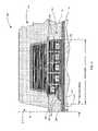
- FIG. 3shows a cross-sectional view of an exemplary transducer 100 of an embodiment of the invention which will be described generally before attention is turned to specific features that provide the improvements described herein.
- the transducer 100comprises a write element 102 and a read element 104 that terminate at a terminus surface.
- the terminus surfaceextends from an air bearing surface (ABS) of a slider and can be either coplanar with the ABS or slightly offset therefrom, usually with a slight amount of recession.
- ABSair bearing surface
- the terminus surfaceis coated with a very thin protective coating (not shown) such as diamond-like or amorphous carbon.
- the read element 104includes a magnetoresistive sensor 106 between two shields, a lower shield 108 and an upper shield that serves as a bottom pole 110 of the write element 102 .
- the exemplary head 100 of FIG. 3is typically referred to as a merged head because the bottom pole 110 functions as a component of both the write element 102 and the read element 104 , however, in non-merged head embodiments the bottom pole of the write element 102 and the upper shield of the read element 104 are separate layers.
- the write element 102includes a yoke 112 which forms a ring having a narrow opening (a “write gap”) that terminates at the terminus surface and that is filled by a write gap layer 114 .
- the yoke 112is preferably made from a high magnetic moment material that can support a magnetic field with a high flux density before becoming saturated (unable to support a higher flux density).
- the yoke 112is formed from the bottom pole 110 , a top pole 116 , a P2 backgap 118 that provides magnetic communication between the top and bottom poles 116 , 110 , and a P2 pole 120 magnetically connected to the top pole 116 .
- the P2 pole 120 and P2 backgap 118are so named because in some embodiments the two are patterned from the same layer, dubbed a P2 layer.
- the bottom pole 110is sometimes referred to as a P1 pole and the top pole 116 is sometimes referred to as a P3 pole.
- the yoke 112can optionally include one or more layers of a magnetic material with a higher magnetic moment than the materials used for the other components of yoke 112 (i.e., P1, P2, and P3 layers), as is well known in the art.
- a hot seed layer 122is one such layer of the higher moment magnetic material.
- the hot seed layer 122is formed between the bottom pole 110 and the write gap layer 114 , and can extend to between the bottom pole 110 and the P2 backgap 118 , as shown in FIG. 3 .
- a portion of the hot seed layer 122is removed and filled with a bottom pole insulation layer 124 .
- the remaining portion of the hot seed layer 122 near the terminus surfaceforms a bottom pole pedestal 126 .
- Another high moment layer 128 of a higher moment magnetic materialcan be formed between the P2 pole 120 and the write gap layer 114 .
- the high moment layer 128is also formed between the P2 backgap 118 and the bottom pole 110 , as shown in FIG. 3 .
- a magnetic fieldis induced within the yoke 112 by passing an electric current through an electrically conductive coil 130 comprising multiple coil turns 132 that are spirally wound around the P2 backgap 118 .
- a heat sink layer 134helps to dissipate heat generated by the coil 130 during writing due to electrical resistance heating.
- the coil 130 and the heat sink layer 134are electrically insulated from each other and from the top and bottom poles 116 , 110 by insulation layers 136 that also serve to insulate the coil turns 132 from each other.
- An additional insulation layer, a zero throat insulation layer 138is also disposed between the coil 130 , the bottom pole 110 , and the P2 pole 120 , as shown in FIG. 3 .
- the zero throat insulation layer 138is discussed further with respect to FIG. 9 .
- the bottom pole 110includes a terminus surface face 140 that is recessed from the terminus surface (TS) by a distance, d.
- the TS face 140can be optionally covered by a TS insulation layer 142 formed, for example, of Al 2 O 3 . Recessing the TS face 140 of the bottom pole 110 from the terminus surface by distance, d, advantageously reduces a deleterious effect known as side writing, as described below with respect to FIGS. 4 and 5 .
- FIGS. 4 and 5show, respectively, write elements of the prior art and an embodiment of the invention as viewed normal to the terminus surface.
- the prior art write elementhas, terminating at the terminus surface, a P2 pole 150 , a high moment layer 152 , a write gap layer 154 , a hot seed layer 156 , and a bottom pole 158 .
- a magnetic fieldis induced in the yoke 112 ( FIG. 3 ) lines of magnetic flux fringe outward around the write gap to form a write field 160 that can interact with a nearby magnetic disk (not shown) to write data bits thereon.
- the common width, W, of the P2 pole 150 , the high moment layer 152 , the write gap layer 154 , and the hot seed layer 156defines the width of the tracks that are written on the magnetic disk. Further, lines of flux that extend laterally beyond the width, W, and interact with the magnetic disk cause the effect known as side writing, which is essentially writing that is outside of the intended track. If tracks are spaced too closely together, side writing from one track will tend to partially overwrite adjacent tracks. Thus, side writing limits how closely tracks can be written to one another and therefore limits data density.
- FIG. 5depicts the reduction in side writing achieved by the recessed TS face 140 ( FIG. 3 ) of an embodiment of the invention.
- the bottom pole 110is shown in dashed lines in FIG. 5 to represent that it is recessed from the terminus surface by a distance, d ( FIG. 3 ), and not exposed at the terminus surface. Recessing the bottom pole 110 reduces the number of lines of magnetic flux that extend laterally beyond the width, W. While recessing the bottom pole 110 reduces side writing, recessing the bottom pole 110 also reduces to a certain extent the amount of magnetic flux that is available within a write field 162 . Accordingly, the distance, d, that the TS face 140 ( FIG.
- the distance, dis more than 0.02 ⁇ m and less than 1.0 ⁇ m.
- a preferable range for dis between about 0.1 ⁇ m and about 0.5 ⁇ m.
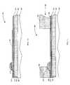
- FIG. 6shows a top view of an exemplary embodiment of a heat sink layer 170 in electrical communication with the coil 130 ( FIG. 3 ; not shown in FIG. 6 ).
- Heat sink layer 170includes a first contact 172 and, in some embodiments, a second contact 174 .
- first contact 172and, in some embodiments, a second contact 174 .
- Electricityfollows a path between the operable contact 172 or 174 and a connecting portion 176 that makes an electrical contact to the coil 130 disposed in a layer below the heat sink layer 170 .
- Turn portion 178makes essentially a complete turn around a backgap portion 180 of the top pole 116 beneath which the P2 backgap 118 ( FIG. 3 ; not shown in FIG. 6 ) is situated.
- heat sink layer 170conducts heat away from the coil 130 ( FIG. 3 ) to lessen pole tip protrusion, as explained in more detail below with respect to FIG. 8 .
- the heat sink layer 170also contributes to inducing a magnetic field in the yoke 112 ( FIG. 3 ) when an electric current is passed therethrough.
- the turn portion 178comprises essentially one turn around the backgap portion 180 of the top pole 116
- the contact 174is the operable contact
- the heat sink layer 170comprises more than one turn. It can be seen, however, that the heat sink layer 170 only passes once beneath the top pole 116 , and therefore the heat sink layer 170 is limited to comprising less than two turns in this embodiment.
- FIG. 7shows a top view of another exemplary embodiment of a heat sink layer 190 that is electrically isolated from the coil 130 ( FIG. 3 ; not shown in FIG. 7 ).
- Heat sink layer 190comprises a turn portion 192 that passes beneath the top pole 116 .
- Turn portion 192makes nearly a complete turn around a backgap portion 194 of the top pole 116 beneath which the P2 backgap 118 ( FIG. 3 ; not shown in FIG. 7 ) is situated.
- the heat sink layer 190 in this embodimentis not in electrical communication with the coil 130 and therefore does not contribute to inducing a magnetic field in the yoke 112 ( FIG. 3 ), the turn portion 192 still preferably forms nearly a complete turn in order to cover the underlying coil 130 as nearly as possible for good heat conduction away from all portions of the coil 130 .
- Heat sink layer 190is disposed adjacent to a conductor layer 194 that includes a first contact 172 and, in some embodiments, a second contact 174 . As above, only one of the contacts 172 , 174 is used, depending on which side of the magnetic disk the head is being used. Electricity follows a path between the operable contact 172 or 174 and a connecting portion 196 that makes an electrical contact to the coil 130 disposed beneath the heat sink layer 190 .
- the coil 130comprises multiple coil turns 132 such that the coil 130 passes beneath the top pole 116 multiple times, whereas the heat sink layers 170 , 190 pass beneath the top pole 116 only once.
- heat sink layer 170 , 190could be replaced with a coil having multiple windings analogous to coil 130 , doing so would require disposing an insulation layer between the multiple turns. In such a design, heat may not be dissipated as efficiently because some of the heat has to follow the spiral pattern of the coil.
- each coil turn 132has a constant thickness (namely a thickness of the coil 130 ) but a potentially varying width.
- the width of each coil turn 132narrows in the region beneath the top pole 116 so that a maximum number of coil turns 132 can pass therethrough.
- the thickness of the coil turns 132is 1 ⁇ m and their widths vary from a minimum of about 0.5 ⁇ m to a maximum of about 2 ⁇ m.
- the aspect ratio of each coil turn 132being the ratio of the width to the height of the coil turn 132 , varies between about 0.5 to about 2.
- the heat sink layers 170 , 190increase this aspect ratio by widening the heat sink layers 170 , 190 as much as is practical.
- the width of the heat sink layer 170 , 190 as measured under the top pole 116 and between the P2 pole 120 and the P2 backgap 118is about 10 ⁇ m.
- a minimum aspect ratiois about 10.
- the remainder of the heat sink layer 170 , 190is considerably wider in this embodiment, and in some embodiments the width of the heat sink layer 170 , 190 reaches a maximum of about 20 ⁇ m to about 30 ⁇ m or more.
- a ratio of the widths of the heat sink layer 170 , 190 to that of a coil turn of the coil layer in this embodiment, where both are measured under the top pole between the P2 pole and the P2 backgapis more than 10, and in some embodiments the ratio is more than 60.
- FIG. 8shows a portion of the write element 102 of FIG. 3 centered on the heat sink layer 134 .
- the insulation layers 136( FIG. 3 ) can be seen to include a P3 insulation layer 200 disposed between the top pole 116 and the heat sink layer 134 , and an upper coil insulation layer 202 between the coil 130 and the heat sink layer 134 .
- the heat sink layer 134is disposed within a volume defined between the P3 insulation layer 200 and the upper coil insulation layer 202 .
- the heat sink layer 134fills the volume, though in other embodiments the heat sink layer 134 only nearly fills the volume.
- Such embodimentscan include, for example, additional insulation layers and/or seed layers.
- the heat sink layer 134serves to lessen pole tip protrusion. More specifically, as an electric current is passed through the coil 130 to induce a magnetic field in the yoke 112 ( FIG. 3 ), the coil 130 generates heat that can cause the coil 130 to expand. This expansion produces a force 204 that causes the write element 102 to distort such that components like the P2 pole 120 protrude beyond the ABS. This pole tip protrusion is deleterious because it decreases the spacing between the head 100 ( FIG. 3 ) and the adjacent magnetic disk (not shown) in the vicinity of the write element 102 . This spacing loss can cause the head 100 to deleteriously contact the magnetic disk.
- heat dissipate heat away from the coil 130 to reduce pole tip protrusionit is desirable to dissipate heat away from the coil 130 to reduce pole tip protrusion.
- Heat dissipationis enhanced by forming the heat sink layer 134 out of a material, such as copper, that has a high coefficient of thermal conductivity. It is important to note, therefore, that good electrical conductivity is not a requirement of the heat sink layer 134 , except it is advantageous in the embodiment shown in FIG. 6 in which the heat sink layer 170 is in electrical communication with the coil 130 .
- the heat sink layer 134extend laterally (in a direction that is within the plane of the heat sink layer 134 and parallel to the terminus surface) within the spatial constraints of the write element 102 , so that excess heat is dissipated through more of the body of the head 100 ( FIG. 3 ).
- the aspect ratio (ratio of width to height) of the heat sink layers 170 ( FIG. 6 ), 190 ( FIG. 7 )is preferably on the order of 20 to 30 or more.
- An embodiment of the inventionallows a zero throat height to be set according to either the position of the zero throat insulation layer 138 ( FIG. 3 ) or the bottom pole pedestal 126 ( FIG. 3 ).
- the zero throat heightis a dimension defined as a distance, measured from the terminus surface, to a parallel plane (zero throat plane) beyond which the write gap begins to widen. For clarity, this dimension is not called out in FIG. 3 , but is instead shown in FIG. 9 , described below. From FIG. 3 it can be seen that the write gap has a uniform thickness, defined by the thickness of the write gap layer 114 , between the bottom pole pedestal 126 and the high moment layer 128 only until a leading edge of the zero throat insulation layer 138 is reached.
- the write gapbegins to widen into a cavity within the yoke 112 that contains the coil 130 and heat sink layer 134 .
- a plane parallel to the terminus surface that intersects the front-most point of the leading edge of the zero throat insulation layer 138is the zero throat plane, and the distance between the zero throat plane and the terminus surface is the zero throat height.
- the zero throat height in FIG. 3is defined by the leading edge 210 ( FIG. 9 ) of the zero throat insulation layer 138
- the zero throat heightis defined by a trailing edge 214 of the bottom pole pedestal 126 . It will be appreciated that in some embodiments the leading edge 210 of the zero throat insulation layer 138 and the trailing edge 214 of the bottom pole pedestal 126 are aligned such that the zero throat height is defined by both.
- An embodiment of the inventionalso illustrated by FIG. 9 , has a shortened yoke length made possible by reducing the spacing between the coil turns 132 and the P2 pole 120 and P2 backgap 118 .
- the yoke lengthis defined as the distance from the zero throat plane to the front of the P2 backgap 118 , as shown.
- the shortened yoke lengthshortens the magnetic path around the yoke 112 thereby increasing the frequency at which the write element 102 can operate.
- shortening the length of the magnetic path around the yoke 112reduces the length of time required to reverse a polarity of a magnetic field within the yoke 112 and therefore increases the number of times the polarity can be reversed in a unit of time.
- An embodiment of the inventionreduces the spacing between the coil turns 132 and the P2 pole 120 and P2 backgap 118 by insulating the P2 pole 120 from a first turn 132 ′ by a thin first inorganic layer 216 , and by insulating the P2 backgap 118 from a last turn 132 ′′ by a thin second inorganic layer 218 .
- the first and second inorganic layers 216 and 218each have a thickness of less than 1.0 ⁇ m, and in some of these embodiments the first and second inorganic layers 216 and 218 each have a thickness in the range of 0.2 ⁇ m to 0.5 ⁇ m.
- the first and second inorganic layers 216 and 218are portions of a lower coil insulation layer 220 additionally disposed between the coil 130 and the bottom pole 110 .
- the zero throat insulation layer 138is disposed between the bottom pole 110 and the first inorganic layer 216 such that the first inorganic layer 216 includes a portion that follows the contour of the zero throat insulation layer 138 and the first turn 132 ′ at least partially overlies the zero throat insulation layer 138 .
- some prior art write elementsinclude a zero throat insulation layer to define the zero throat height
- none of these prior art devicesinclude a thin inorganic insulation layer between a P2 pole and a first coil turn because of the difficulty in forming the first coil turn at least partially over the zero throat insulation layer.
- the prior art devices that have included the zero throat insulation layerhave also included a thick organic insulation layer, such as baked photoresist, disposed between a P2 pole and a first coil turn.
- a thick organic insulation layersuch as baked photoresist
- the first turn 132 ′can be placed closer to the P2 pole 120 , thus reducing the yoke length.
- Embodiments of the inventioncan also provide methods for fabricating a write element with a reduced yoke length, illustrated in FIGS. 10-18 by cross-sectional views of a partially fabricated write element at successive steps of an exemplary embodiment of the method.
- An embodiment of the methodcomprises forming a base layer including a bottom pole and a zero throat insulation layer disposed over the bottom pole, and forming a cover insulation layer over the base layer.
- An embodiment of the methodfurther comprises forming an anti-reflective coating (ARC) layer over the cover layer and forming a mask layer, including a spiral coil opening, over the ARC layer.
- ARCanti-reflective coating
- the ARC layersuppresses undesirable reflections off of certain features of the partially fabricated device, such as the zero throat insulation layer, to allow portions of the mask layer to be formed near or on such features.
- An embodiment of the methodfurther comprises forming a coil layer comprising coil turns within the coil opening, removing the mask layer to form a spiral coil insulation opening, forming a coil insulation layer within the spiral coil insulation opening, and forming a top layer over the coil layer.
- forming a base layer 300includes forming a bottom pole 302 over a substrate 304 .
- the substrate 304can be any suitably flat support layer, such as a polished silicon wafer.
- the substrate 304can also comprise the layers of a read element, such as those layers of the read element 104 that are disposed beneath the bottom pole 110 in FIG. 3 .
- the bottom pole 302can be formed of a high magnetic moment material such as most nickel-iron alloys and cobalt-nickel-iron alloys.
- the bottom pole 302can be formed, for example, by plating.
- the bottom pole 302is formed to provide for a recessed TS face 306 and a TS insulation layer 308 . This can be achieved, for instance, by masking so that the bottom pole 302 is not plated within the area that will be filled by the TS insulation layer 308 .
- a layer of a protective materialsuch as alumina (Al 2 O 3 ), is deposited, for example, by sputtering, to create the TS insulation layer 308 .
- forming the base layer 300also includes forming a hot seed layer 310 over the bottom pole 302 .
- the hot seed layer 310is preferably formed of a high moment magnetic material with a higher magnetic moment than the bottom pole 302 .
- higher magnetic moment materialsinclude Ni 45 Fe 55 and iron nitride compounds such as FeN, FeRhN, and FeTaN. These materials can also be deposited by masking and sputtering.
- a bottom pole pedestal 312is optionally formed from the hot seed layer 310 , for instance, by masking an area that will become the bottom pole pedestal 312 and etching a remaining exposed area.
- the hot seed layer 310 in the etched areacan be partially etched, as shown in FIG. 10 , or completely removed to expose the bottom pole 302 . The etching can also be extended into the bottom pole 302 in some embodiments.
- the etched area behind the bottom pole pedestal 312is filled with a dielectric material, such as Al 2 O 3 , to form a bottom pole insulation layer 314 .
- the bottom pole insulation layer 314can be formed, for example, by sputtering a layer of Al 2 O 3 to a depth that exceeds the height of the bottom pole pedestal 312 followed by a planarization process such as chemical-mechanical polishing (CMP).
- Forming the base layer 300can also comprise forming a write gap layer 316 .
- the write gap layer 316can also be formed by masking and sputtering and can be formed from a number of suitable low magnetic saturation materials including NiNb, NiCr, and Al 2 O 3 . Although the write gap layer 316 is shown in FIG. 10 as extending to completely cover the bottom pole insulation layer 314 , it will be appreciated that the write gap layer 316 need not extend nearly so far. Other configurations for the write gap layer 316 will be discussed in more detail below.
- Forming the base layer 300can also comprise forming a zero throat insulation layer 318 disposed over the bottom pole 302 .
- the zero throat insulation layer 318can be formed by masking followed by sputtering an insulating material such as Al 2 O 3 . Alternately, the zero throat insulation layer 318 can be formed from cured photoresist through a photolithography process. In those embodiments that include the hot seed layer 310 , the zero throat insulation layer 318 can be formed over the bottom pole pedestal 312 or over the bottom pole insulation layer 314 , or partially over both, as illustrated in FIG. 10 . In some embodiments the write gap layer 316 extends between the zero throat insulation layer 318 and the bottom pole 302 .
- the zero throat insulation layer 318is formed before the write gap layer 316 and then the write gap layer 316 is deposited. In these embodiments, the write gap layer 316 can optionally cover the zero throat insulation layer 318 . In some embodiments the write gap layer 316 extends only as far as the zero throat insulation layer 318 . In these embodiments either the write gap layer 316 or the zero throat insulation layer 318 can be formed first.
- Forming the base layer 300can also comprise forming a P2 layer 320 including a P2 pole 322 and a P2 backgap 324 .
- the P2 layer 320can be formed of a high magnetic moment material such as a NiFe or CoNiFe alloy by masking and plating.
- forming the base layer 300also includes forming a high moment layer 326 between the P2 pole 322 and the write gap layer 316 .
- the high moment layer 326can additionally be formed between the P2 pole 322 and the zero throat insulation layer 318 , and between the P2 backgap 324 and the bottom pole 302 .
- the high moment layer 326is similar to the hot seed layer 310 and preferably formed of a high moment magnetic material with a higher magnetic moment than the material of the P2 layer 320 .
- the high moment layer 326is likewise preferably deposited by masking and sputtering.
- the high moment layer 326 and the hot seed layer 310are made from the same material.
- the high moment layer 326is formed before the P2 layer 320 .
- An embodiment of the method of the inventionalso comprises forming a cover insulation layer 330 over the base layer 300 , as shown in FIG. 12 .
- the cover insulation layer 330will become the lower coil insulation layer 220 ( FIG. 9 ) that includes the first and second inorganic layers 216 and 218 ( FIG. 9 ) in the completed write element.
- the cover insulation layer 330can be formed from an inorganic material, such as Al 2 O 3 , for example, by sputtering. It can be seen in the embodiment of FIG. 12 that the cover insulation layer 330 blankets the top surfaces of the base layer 330 .
- the cover insulation layer 330should be kept very thin.
- the cover insulation layer 330is formed to a thickness, t, of less than 1.0 ⁇ m. Accordingly, the first and second inorganic layers 216 and 218 ( FIG. 9 ) can each be made to have a thickness of less than 1.0 ⁇ m.
- the cover insulation layer 330tends to be deposited with a reduced thickness on vertical surfaces compared to horizontal surfaces, the first and second inorganic layers 216 and 218 can each have a thickness in the range of about 0.2 ⁇ m to about 0.5 ⁇ m.
- an embodiment of the method of the inventioncan also comprise forming a seed layer 332 and an anti-reflective coating (ARC) layer 334 over the cover layer 330 .
- the seed layer 332is a very thin layer of an electrically conductive material such as copper.
- the seed layer 332serves as an electrode during the subsequent plating of a coil layer 342 , discussed below with respect to FIG. 15 .
- the ARC layer 334is formed over the cover layer 330 and particularly over an exposed portion of the zero throat insulation layer 318 , the importance of which is described in detail below with respect to FIG. 13 .
- the ARC layer 334is formed over the seed layer 332 .
- Forming the ARC layer 334includes depositing a silicon nitride compound such as SiN x or SiON x .
- the ARC layer 334is preferably deposited to a thickness of about 80 ⁇ to about 200 ⁇ , and more preferably to a thickness of about 160 ⁇ .
- a method of an embodiment of the inventionalso comprises forming a mask layer 336 , including a spiral coil opening 338 , over the ARC layer 334 .
- the mask layer 336can be formed by standard photolithographic processes including spin coating undeveloped photoresist over the ARC layer 334 , exposing the photoresist to a patterned illumination, developing the photoresist, and removing undeveloped photoresist to leave the mask layer 336 .
- the ARC layer 334allows portions of the mask layer 336 , such as mask portion 340 , to be formed either on, or near (as illustrated in FIG. 13 ) the zero throat insulation layer 318 .
- the curvature of the zero throat insulation layer 318prevents the formation of photoresist features on or near the zero throat insulation layer 318 . It is the ability to form the mask portion 340 on or near the zero throat insulation layer 318 that allows the first turn 132 ′ ( FIG. 9 ) to be formed between the mask portion 340 and the P2 pole 322 .
- reflections off of the zero throat insulation layer 318are not the only reflections that can cause problems with forming the mask layer 336 . Accordingly, the ARC layer 334 is additionally beneficial for suppressing reflections off of the vertical sidewalls of the P2 pole 322 and the P2 backgap 324 .
- An embodiment of the method of the inventionalso comprises forming the coil layer 342 ( FIG. 15 ) comprising coil turns 344 ( FIG. 15 ).
- forming the coil layer 342can include selectively removing the ARC layer 334 where exposed by the spiral coil opening 338 . Selectively removing the ARC layer 334 exposes the seed layer 332 for subsequently plating the coil layer 342 .
- the ARC layer 334can be removed, for example, by reactive ion etching (RIE).
- the coil layer 342is preferably formed from a highly conductive material such as copper. In some embodiments, as shown, the plating extends over the P2 pole 322 and the P2 backgap 324 . It will be appreciated that the coil layer 342 can also be formed by other methods, such as sputtering, though plating is a preferred technique because it can deposit a relatively thick layer comparatively quickly.
- the seed layer 332provides an electrode that allows the coil layer 342 to be plated, as noted above, however in some embodiments that do not form the coil layer 342 by plating the seed layer 332 is not necessary.
- Some embodiments of the inventionfurther comprise forming a spiral coil insulation opening 346 between the coil turns 344 by removing the mask layer 336 , as shown in FIG. 16 .
- Forming the spiral coil insulation opening 346also includes removing the ARC layer 334 ( FIG. 15 ) where exposed by the removal of the mask layer 336 , and removing the seed layer 332 ( FIG. 15 ) where exposed by the removal of the ARC layer 334 .
- the mask layer 336can be removed, for example, by wet chemical stripping as commonly used in photolithography processes.
- the ARC layer 334can be removed, for example, by RIE.
- the seed layer 332can be removed, for instance, by ion milling. In FIG. 16 , and subsequent drawings, the seed layer 332 beneath the coil turns 344 is omitted as the seed layer 332 becomes part of the coil turns 344 as the coil turns 344 are plated.
- Some embodiments of the inventionfurther comprise forming a spiral coil insulation layer 348 within the spiral coil insulation opening 346 and between the coil turns 344 , as shown in FIG. 17 .
- Forming the spiral coil insulation layer 348can be achieved, for example, by depositing a blanket layer 350 of a dielectric material such as Al 2 O 3 .
- Forming the spiral coil insulation layer 348can be completed by planarizing to remove excess materials and produce a planar surface 352 upon which further layers can be formed.
- the planar surface 352exposes the P2 pole 322 and the P2 backgap 324 so that a P3 layer (top pole 116 in FIG. 3 ) can be joined thereto.
- CMPis one method of planarizing to form the planar surface 352 .
- the level of the planar surface 352is one of the parameters that can vary between embodiments. For example, by continuing the planarization to produce a lower planar surface 352 than the one shown in FIG. 18 would produce a structure more similar to the one shown in FIG. 3 .
- Some embodiments of the inventionfurther comprise forming a top layer over the coil layer 342 ( FIG. 15 ). More specifically, the top layer is formed on the planar surface 352 ( FIG. 18 ).
- the top layercomprises a relatively flat P3 layer joined to the P2 pole 322 and P2 backgap 324 , and an insulation layer, such as upper coil insulation layer 202 ( FIG. 8 ), disposed between the coil layer 342 and the P3 layer.
- the P3 layeris substantially as shown as top pole 116 ( FIG. 3 ) so as to also include either a heat sink layer 134 ( FIG. 3 ) or a second coil layer.
- the techniques to form the further layers of the top layeris much as described above.
- a height of the heat sink layer 134 or the second coil layeris a design criteria that can be varied to alter an efficiency of the write element.
- efficiencyis a measure of the strength of the write field 162 ( FIG. 5 ) for a given amount of electrical current input to the coil 130 ( FIG. 3 ) compared with a theoretical maximum strength.
- the height of the heat sink layer 134 or the second coil layereffects the length of the over-all magnetic path around the yoke 112 ( FIG. 3 ) and an over-all separation between the bottom and top poles 110 , 116 ( FIG. 3 ).
- efficiencyis increased by further separation between the bottom and top poles 110 , 116 , efficiency is reduced by the increased magnetic path length caused by increased separation. It will be appreciated that efficiency is optimized for different embodiments of the write element of the invention at different over-all separations between the bottom and top poles 110 , 116 .
- the optimized separationcan be achieved, in some embodiments, by selecting an optimized height of the heat sink layer 134 or the second coil layer once the thicknesses of the other layers of the write element have been specified.
Landscapes
- Physics & Mathematics (AREA)
- Electromagnetism (AREA)
- Engineering & Computer Science (AREA)
- Manufacturing & Machinery (AREA)
- Magnetic Heads (AREA)
Abstract
Description
Claims (13)
Priority Applications (1)
| Application Number | Priority Date | Filing Date | Title |
|---|---|---|---|
| US10/909,226US7522379B1 (en) | 2004-07-30 | 2004-07-30 | Write element with recessed pole and heat sink layer for ultra-high density writing |
Applications Claiming Priority (1)
| Application Number | Priority Date | Filing Date | Title |
|---|---|---|---|
| US10/909,226US7522379B1 (en) | 2004-07-30 | 2004-07-30 | Write element with recessed pole and heat sink layer for ultra-high density writing |
Publications (1)
| Publication Number | Publication Date |
|---|---|
| US7522379B1true US7522379B1 (en) | 2009-04-21 |
Family
ID=40550425
Family Applications (1)
| Application Number | Title | Priority Date | Filing Date |
|---|---|---|---|
| US10/909,226Expired - Fee RelatedUS7522379B1 (en) | 2004-07-30 | 2004-07-30 | Write element with recessed pole and heat sink layer for ultra-high density writing |
Country Status (1)
| Country | Link |
|---|---|
| US (1) | US7522379B1 (en) |
Cited By (136)
| Publication number | Priority date | Publication date | Assignee | Title |
|---|---|---|---|---|
| US8248896B1 (en) | 2010-06-24 | 2012-08-21 | Western Digital (Fremont), Llc | Method and system for providing an energy assisted magnetic recording disk drive having improved heat dissipation |
| US8628672B1 (en) | 2012-06-27 | 2014-01-14 | Western Digital (Fremont), Llc | Process for manufacturing a perpendicular magnetic recording writer pole with nonmagnetic bevel |
| US8703397B1 (en) | 2012-03-29 | 2014-04-22 | Western Digital (Fremont), Llc | Method for providing side shields for a magnetic recording transducer |
| US8797686B1 (en) | 2010-12-23 | 2014-08-05 | Western Digital (Fremont), Llc | Magnetic recording transducer with short effective throat height and method of fabrication |
| US8830628B1 (en) | 2009-02-23 | 2014-09-09 | Western Digital (Fremont), Llc | Method and system for providing a perpendicular magnetic recording head |
| US8879207B1 (en) | 2011-12-20 | 2014-11-04 | Western Digital (Fremont), Llc | Method for providing a side shield for a magnetic recording transducer using an air bridge |
| US8883017B1 (en) | 2013-03-12 | 2014-11-11 | Western Digital (Fremont), Llc | Method and system for providing a read transducer having seamless interfaces |
| US8917581B1 (en) | 2013-12-18 | 2014-12-23 | Western Digital Technologies, Inc. | Self-anneal process for a near field transducer and chimney in a hard disk drive assembly |
| US8923102B1 (en) | 2013-07-16 | 2014-12-30 | Western Digital (Fremont), Llc | Optical grating coupling for interferometric waveguides in heat assisted magnetic recording heads |
| US8947985B1 (en) | 2013-07-16 | 2015-02-03 | Western Digital (Fremont), Llc | Heat assisted magnetic recording transducers having a recessed pole |
| US8953422B1 (en) | 2014-06-10 | 2015-02-10 | Western Digital (Fremont), Llc | Near field transducer using dielectric waveguide core with fine ridge feature |
| US8958272B1 (en) | 2014-06-10 | 2015-02-17 | Western Digital (Fremont), Llc | Interfering near field transducer for energy assisted magnetic recording |
| US8970988B1 (en) | 2013-12-31 | 2015-03-03 | Western Digital (Fremont), Llc | Electric gaps and method for making electric gaps for multiple sensor arrays |
| US8971160B1 (en) | 2013-12-19 | 2015-03-03 | Western Digital (Fremont), Llc | Near field transducer with high refractive index pin for heat assisted magnetic recording |
| US8976635B1 (en) | 2014-06-10 | 2015-03-10 | Western Digital (Fremont), Llc | Near field transducer driven by a transverse electric waveguide for energy assisted magnetic recording |
| US8980109B1 (en) | 2012-12-11 | 2015-03-17 | Western Digital (Fremont), Llc | Method for providing a magnetic recording transducer using a combined main pole and side shield CMP for a wraparound shield scheme |
| US8982508B1 (en) | 2011-10-31 | 2015-03-17 | Western Digital (Fremont), Llc | Method for providing a side shield for a magnetic recording transducer |
| US8984740B1 (en) | 2012-11-30 | 2015-03-24 | Western Digital (Fremont), Llc | Process for providing a magnetic recording transducer having a smooth magnetic seed layer |
| US8988825B1 (en) | 2014-02-28 | 2015-03-24 | Western Digital (Fremont, LLC | Method for fabricating a magnetic writer having half-side shields |
| US8988812B1 (en) | 2013-11-27 | 2015-03-24 | Western Digital (Fremont), Llc | Multi-sensor array configuration for a two-dimensional magnetic recording (TDMR) operation |
| US8995087B1 (en) | 2006-11-29 | 2015-03-31 | Western Digital (Fremont), Llc | Perpendicular magnetic recording write head having a wrap around shield |
| US8993217B1 (en) | 2013-04-04 | 2015-03-31 | Western Digital (Fremont), Llc | Double exposure technique for high resolution disk imaging |
| US9001467B1 (en) | 2014-03-05 | 2015-04-07 | Western Digital (Fremont), Llc | Method for fabricating side shields in a magnetic writer |
| US8997832B1 (en) | 2010-11-23 | 2015-04-07 | Western Digital (Fremont), Llc | Method of fabricating micrometer scale components |
| US9001628B1 (en) | 2013-12-16 | 2015-04-07 | Western Digital (Fremont), Llc | Assistant waveguides for evaluating main waveguide coupling efficiency and diode laser alignment tolerances for hard disk |
| US9007719B1 (en) | 2013-10-23 | 2015-04-14 | Western Digital (Fremont), Llc | Systems and methods for using double mask techniques to achieve very small features |
| US9007879B1 (en) | 2014-06-10 | 2015-04-14 | Western Digital (Fremont), Llc | Interfering near field transducer having a wide metal bar feature for energy assisted magnetic recording |
| US9007725B1 (en) | 2014-10-07 | 2015-04-14 | Western Digital (Fremont), Llc | Sensor with positive coupling between dual ferromagnetic free layer laminates |
| US9013836B1 (en) | 2013-04-02 | 2015-04-21 | Western Digital (Fremont), Llc | Method and system for providing an antiferromagnetically coupled return pole |
| US9042058B1 (en) | 2013-10-17 | 2015-05-26 | Western Digital Technologies, Inc. | Shield designed for middle shields in a multiple sensor array |
| US9042051B2 (en) | 2013-08-15 | 2015-05-26 | Western Digital (Fremont), Llc | Gradient write gap for perpendicular magnetic recording writer |
| US9042057B1 (en) | 2013-01-09 | 2015-05-26 | Western Digital (Fremont), Llc | Methods for providing magnetic storage elements with high magneto-resistance using Heusler alloys |
| US9042208B1 (en) | 2013-03-11 | 2015-05-26 | Western Digital Technologies, Inc. | Disk drive measuring fly height by applying a bias voltage to an electrically insulated write component of a head |
| US9042052B1 (en) | 2014-06-23 | 2015-05-26 | Western Digital (Fremont), Llc | Magnetic writer having a partially shunted coil |
| US9053735B1 (en) | 2014-06-20 | 2015-06-09 | Western Digital (Fremont), Llc | Method for fabricating a magnetic writer using a full-film metal planarization |
| US9064528B1 (en) | 2013-05-17 | 2015-06-23 | Western Digital Technologies, Inc. | Interferometric waveguide usable in shingled heat assisted magnetic recording in the absence of a near-field transducer |
| US9064507B1 (en) | 2009-07-31 | 2015-06-23 | Western Digital (Fremont), Llc | Magnetic etch-stop layer for magnetoresistive read heads |
| US9065043B1 (en) | 2012-06-29 | 2015-06-23 | Western Digital (Fremont), Llc | Tunnel magnetoresistance read head with narrow shield-to-shield spacing |
| US9064527B1 (en) | 2013-04-12 | 2015-06-23 | Western Digital (Fremont), Llc | High order tapered waveguide for use in a heat assisted magnetic recording head |
| US9070381B1 (en) | 2013-04-12 | 2015-06-30 | Western Digital (Fremont), Llc | Magnetic recording read transducer having a laminated free layer |
| US9082423B1 (en) | 2013-12-18 | 2015-07-14 | Western Digital (Fremont), Llc | Magnetic recording write transducer having an improved trailing surface profile |
| US9087527B1 (en) | 2014-10-28 | 2015-07-21 | Western Digital (Fremont), Llc | Apparatus and method for middle shield connection in magnetic recording transducers |
| US9087534B1 (en) | 2011-12-20 | 2015-07-21 | Western Digital (Fremont), Llc | Method and system for providing a read transducer having soft and hard magnetic bias structures |
| US9093639B2 (en) | 2012-02-21 | 2015-07-28 | Western Digital (Fremont), Llc | Methods for manufacturing a magnetoresistive structure utilizing heating and cooling |
| US9104107B1 (en) | 2013-04-03 | 2015-08-11 | Western Digital (Fremont), Llc | DUV photoresist process |
| US9111550B1 (en) | 2014-12-04 | 2015-08-18 | Western Digital (Fremont), Llc | Write transducer having a magnetic buffer layer spaced between a side shield and a write pole by non-magnetic layers |
| US9111564B1 (en) | 2013-04-02 | 2015-08-18 | Western Digital (Fremont), Llc | Magnetic recording writer having a main pole with multiple flare angles |
| US9111558B1 (en) | 2014-03-14 | 2015-08-18 | Western Digital (Fremont), Llc | System and method of diffractive focusing of light in a waveguide |
| US9123362B1 (en) | 2011-03-22 | 2015-09-01 | Western Digital (Fremont), Llc | Methods for assembling an electrically assisted magnetic recording (EAMR) head |
| US9123359B1 (en) | 2010-12-22 | 2015-09-01 | Western Digital (Fremont), Llc | Magnetic recording transducer with sputtered antiferromagnetic coupling trilayer between plated ferromagnetic shields and method of fabrication |
| US9123374B1 (en) | 2015-02-12 | 2015-09-01 | Western Digital (Fremont), Llc | Heat assisted magnetic recording writer having an integrated polarization rotation plate |
| US9123358B1 (en) | 2012-06-11 | 2015-09-01 | Western Digital (Fremont), Llc | Conformal high moment side shield seed layer for perpendicular magnetic recording writer |
| US9135937B1 (en) | 2014-05-09 | 2015-09-15 | Western Digital (Fremont), Llc | Current modulation on laser diode for energy assisted magnetic recording transducer |
| US9135930B1 (en) | 2014-03-06 | 2015-09-15 | Western Digital (Fremont), Llc | Method for fabricating a magnetic write pole using vacuum deposition |
| US9142233B1 (en) | 2014-02-28 | 2015-09-22 | Western Digital (Fremont), Llc | Heat assisted magnetic recording writer having a recessed pole |
| US9147408B1 (en) | 2013-12-19 | 2015-09-29 | Western Digital (Fremont), Llc | Heated AFM layer deposition and cooling process for TMR magnetic recording sensor with high pinning field |
| US9147404B1 (en) | 2015-03-31 | 2015-09-29 | Western Digital (Fremont), Llc | Method and system for providing a read transducer having a dual free layer |
| US9153255B1 (en) | 2014-03-05 | 2015-10-06 | Western Digital (Fremont), Llc | Method for fabricating a magnetic writer having an asymmetric gap and shields |
| US9183854B2 (en) | 2014-02-24 | 2015-11-10 | Western Digital (Fremont), Llc | Method to make interferometric taper waveguide for HAMR light delivery |
| US9190085B1 (en) | 2014-03-12 | 2015-11-17 | Western Digital (Fremont), Llc | Waveguide with reflective grating for localized energy intensity |
| US9190079B1 (en) | 2014-09-22 | 2015-11-17 | Western Digital (Fremont), Llc | Magnetic write pole having engineered radius of curvature and chisel angle profiles |
| US9194692B1 (en) | 2013-12-06 | 2015-11-24 | Western Digital (Fremont), Llc | Systems and methods for using white light interferometry to measure undercut of a bi-layer structure |
| US9202480B2 (en) | 2009-10-14 | 2015-12-01 | Western Digital (Fremont), LLC. | Double patterning hard mask for damascene perpendicular magnetic recording (PMR) writer |
| US9202493B1 (en) | 2014-02-28 | 2015-12-01 | Western Digital (Fremont), Llc | Method of making an ultra-sharp tip mode converter for a HAMR head |
| US9214169B1 (en) | 2014-06-20 | 2015-12-15 | Western Digital (Fremont), Llc | Magnetic recording read transducer having a laminated free layer |
| US9214172B2 (en) | 2013-10-23 | 2015-12-15 | Western Digital (Fremont), Llc | Method of manufacturing a magnetic read head |
| US9213322B1 (en) | 2012-08-16 | 2015-12-15 | Western Digital (Fremont), Llc | Methods for providing run to run process control using a dynamic tuner |
| US9214165B1 (en) | 2014-12-18 | 2015-12-15 | Western Digital (Fremont), Llc | Magnetic writer having a gradient in saturation magnetization of the shields |
| US9230565B1 (en) | 2014-06-24 | 2016-01-05 | Western Digital (Fremont), Llc | Magnetic shield for magnetic recording head |
| US9236560B1 (en) | 2014-12-08 | 2016-01-12 | Western Digital (Fremont), Llc | Spin transfer torque tunneling magnetoresistive device having a laminated free layer with perpendicular magnetic anisotropy |
| US9245545B1 (en) | 2013-04-12 | 2016-01-26 | Wester Digital (Fremont), Llc | Short yoke length coils for magnetic heads in disk drives |
| US9245562B1 (en) | 2015-03-30 | 2016-01-26 | Western Digital (Fremont), Llc | Magnetic recording writer with a composite main pole |
| US9245543B1 (en) | 2010-06-25 | 2016-01-26 | Western Digital (Fremont), Llc | Method for providing an energy assisted magnetic recording head having a laser integrally mounted to the slider |
| US9251813B1 (en) | 2009-04-19 | 2016-02-02 | Western Digital (Fremont), Llc | Method of making a magnetic recording head |
| US9263067B1 (en) | 2013-05-29 | 2016-02-16 | Western Digital (Fremont), Llc | Process for making PMR writer with constant side wall angle |
| US9263071B1 (en) | 2015-03-31 | 2016-02-16 | Western Digital (Fremont), Llc | Flat NFT for heat assisted magnetic recording |
| US9269382B1 (en) | 2012-06-29 | 2016-02-23 | Western Digital (Fremont), Llc | Method and system for providing a read transducer having improved pinning of the pinned layer at higher recording densities |
| US9275657B1 (en) | 2013-08-14 | 2016-03-01 | Western Digital (Fremont), Llc | Process for making PMR writer with non-conformal side gaps |
| US9280990B1 (en) | 2013-12-11 | 2016-03-08 | Western Digital (Fremont), Llc | Method for fabricating a magnetic writer using multiple etches |
| US9286919B1 (en) | 2014-12-17 | 2016-03-15 | Western Digital (Fremont), Llc | Magnetic writer having a dual side gap |
| US9287494B1 (en) | 2013-06-28 | 2016-03-15 | Western Digital (Fremont), Llc | Magnetic tunnel junction (MTJ) with a magnesium oxide tunnel barrier |
| US9305583B1 (en) | 2014-02-18 | 2016-04-05 | Western Digital (Fremont), Llc | Method for fabricating a magnetic writer using multiple etches of damascene materials |
| US9312064B1 (en) | 2015-03-02 | 2016-04-12 | Western Digital (Fremont), Llc | Method to fabricate a magnetic head including ion milling of read gap using dual layer hard mask |
| US9318130B1 (en) | 2013-07-02 | 2016-04-19 | Western Digital (Fremont), Llc | Method to fabricate tunneling magnetic recording heads with extended pinned layer |
| US9336814B1 (en) | 2013-03-12 | 2016-05-10 | Western Digital (Fremont), Llc | Inverse tapered waveguide for use in a heat assisted magnetic recording head |
| US9343086B1 (en) | 2013-09-11 | 2016-05-17 | Western Digital (Fremont), Llc | Magnetic recording write transducer having an improved sidewall angle profile |
| US9343098B1 (en) | 2013-08-23 | 2016-05-17 | Western Digital (Fremont), Llc | Method for providing a heat assisted magnetic recording transducer having protective pads |
| US9343087B1 (en) | 2014-12-21 | 2016-05-17 | Western Digital (Fremont), Llc | Method for fabricating a magnetic writer having half shields |
| US9349392B1 (en) | 2012-05-24 | 2016-05-24 | Western Digital (Fremont), Llc | Methods for improving adhesion on dielectric substrates |
| US9349394B1 (en) | 2013-10-18 | 2016-05-24 | Western Digital (Fremont), Llc | Method for fabricating a magnetic writer having a gradient side gap |
| US9361912B1 (en)* | 2015-04-20 | 2016-06-07 | Headway Technologies, Inc. | High moment side shield design for area density improvement of perpendicular magnetic recording (PMR) writer |
| US9361913B1 (en) | 2013-06-03 | 2016-06-07 | Western Digital (Fremont), Llc | Recording read heads with a multi-layer AFM layer methods and apparatuses |
| US9361914B1 (en) | 2014-06-18 | 2016-06-07 | Western Digital (Fremont), Llc | Magnetic sensor with thin capping layer |
| US9368134B1 (en) | 2010-12-16 | 2016-06-14 | Western Digital (Fremont), Llc | Method and system for providing an antiferromagnetically coupled writer |
| US9384765B1 (en) | 2015-09-24 | 2016-07-05 | Western Digital (Fremont), Llc | Method and system for providing a HAMR writer having improved optical efficiency |
| US9384763B1 (en) | 2015-03-26 | 2016-07-05 | Western Digital (Fremont), Llc | Dual free layer magnetic reader having a rear bias structure including a soft bias layer |
| US9396742B1 (en) | 2012-11-30 | 2016-07-19 | Western Digital (Fremont), Llc | Magnetoresistive sensor for a magnetic storage system read head, and fabrication method thereof |
| US9396743B1 (en) | 2014-02-28 | 2016-07-19 | Western Digital (Fremont), Llc | Systems and methods for controlling soft bias thickness for tunnel magnetoresistance readers |
| US9406331B1 (en) | 2013-06-17 | 2016-08-02 | Western Digital (Fremont), Llc | Method for making ultra-narrow read sensor and read transducer device resulting therefrom |
| US9424866B1 (en) | 2015-09-24 | 2016-08-23 | Western Digital (Fremont), Llc | Heat assisted magnetic recording write apparatus having a dielectric gap |
| US9431032B1 (en) | 2013-08-14 | 2016-08-30 | Western Digital (Fremont), Llc | Electrical connection arrangement for a multiple sensor array usable in two-dimensional magnetic recording |
| US9431038B1 (en) | 2015-06-29 | 2016-08-30 | Western Digital (Fremont), Llc | Method for fabricating a magnetic write pole having an improved sidewall angle profile |
| US9431047B1 (en) | 2013-05-01 | 2016-08-30 | Western Digital (Fremont), Llc | Method for providing an improved AFM reader shield |
| US9431031B1 (en) | 2015-03-24 | 2016-08-30 | Western Digital (Fremont), Llc | System and method for magnetic transducers having multiple sensors and AFC shields |
| US9431039B1 (en) | 2013-05-21 | 2016-08-30 | Western Digital (Fremont), Llc | Multiple sensor array usable in two-dimensional magnetic recording |
| US9437251B1 (en) | 2014-12-22 | 2016-09-06 | Western Digital (Fremont), Llc | Apparatus and method having TDMR reader to reader shunts |
| US9443541B1 (en) | 2015-03-24 | 2016-09-13 | Western Digital (Fremont), Llc | Magnetic writer having a gradient in saturation magnetization of the shields and return pole |
| US9441938B1 (en) | 2013-10-08 | 2016-09-13 | Western Digital (Fremont), Llc | Test structures for measuring near field transducer disc length |
| US9449621B1 (en) | 2015-03-26 | 2016-09-20 | Western Digital (Fremont), Llc | Dual free layer magnetic reader having a rear bias structure having a high aspect ratio |
| US9449625B1 (en) | 2014-12-24 | 2016-09-20 | Western Digital (Fremont), Llc | Heat assisted magnetic recording head having a plurality of diffusion barrier layers |
| US9472216B1 (en) | 2015-09-23 | 2016-10-18 | Western Digital (Fremont), Llc | Differential dual free layer magnetic reader |
| US9484051B1 (en) | 2015-11-09 | 2016-11-01 | The Provost, Fellows, Foundation Scholars and the other members of Board, of the College of the Holy and Undivided Trinity of Queen Elizabeth near Dublin | Method and system for reducing undesirable reflections in a HAMR write apparatus |
| US9508363B1 (en) | 2014-06-17 | 2016-11-29 | Western Digital (Fremont), Llc | Method for fabricating a magnetic write pole having a leading edge bevel |
| US9508372B1 (en) | 2015-06-03 | 2016-11-29 | Western Digital (Fremont), Llc | Shingle magnetic writer having a low sidewall angle pole |
| US9508365B1 (en) | 2015-06-24 | 2016-11-29 | Western Digital (Fremont), LLC. | Magnetic reader having a crystal decoupling structure |
| US9530443B1 (en) | 2015-06-25 | 2016-12-27 | Western Digital (Fremont), Llc | Method for fabricating a magnetic recording device having a high aspect ratio structure |
| US9564150B1 (en) | 2015-11-24 | 2017-02-07 | Western Digital (Fremont), Llc | Magnetic read apparatus having an improved read sensor isolation circuit |
| US9595273B1 (en) | 2015-09-30 | 2017-03-14 | Western Digital (Fremont), Llc | Shingle magnetic writer having nonconformal shields |
| US9646639B2 (en) | 2015-06-26 | 2017-05-09 | Western Digital (Fremont), Llc | Heat assisted magnetic recording writer having integrated polarization rotation waveguides |
| US9666214B1 (en) | 2015-09-23 | 2017-05-30 | Western Digital (Fremont), Llc | Free layer magnetic reader that may have a reduced shield-to-shield spacing |
| US9721595B1 (en) | 2014-12-04 | 2017-08-01 | Western Digital (Fremont), Llc | Method for providing a storage device |
| US9741366B1 (en) | 2014-12-18 | 2017-08-22 | Western Digital (Fremont), Llc | Method for fabricating a magnetic writer having a gradient in saturation magnetization of the shields |
| US9740805B1 (en) | 2015-12-01 | 2017-08-22 | Western Digital (Fremont), Llc | Method and system for detecting hotspots for photolithographically-defined devices |
| US9754611B1 (en) | 2015-11-30 | 2017-09-05 | Western Digital (Fremont), Llc | Magnetic recording write apparatus having a stepped conformal trailing shield |
| US9767831B1 (en) | 2015-12-01 | 2017-09-19 | Western Digital (Fremont), Llc | Magnetic writer having convex trailing surface pole and conformal write gap |
| US9786301B1 (en) | 2014-12-02 | 2017-10-10 | Western Digital (Fremont), Llc | Apparatuses and methods for providing thin shields in a multiple sensor array |
| US9799351B1 (en) | 2015-11-30 | 2017-10-24 | Western Digital (Fremont), Llc | Short yoke length writer having assist coils |
| US9812155B1 (en) | 2015-11-23 | 2017-11-07 | Western Digital (Fremont), Llc | Method and system for fabricating high junction angle read sensors |
| US9842615B1 (en) | 2015-06-26 | 2017-12-12 | Western Digital (Fremont), Llc | Magnetic reader having a nonmagnetic insertion layer for the pinning layer |
| US9858951B1 (en) | 2015-12-01 | 2018-01-02 | Western Digital (Fremont), Llc | Method for providing a multilayer AFM layer in a read sensor |
| US9881638B1 (en) | 2014-12-17 | 2018-01-30 | Western Digital (Fremont), Llc | Method for providing a near-field transducer (NFT) for a heat assisted magnetic recording (HAMR) device |
| US9934811B1 (en) | 2014-03-07 | 2018-04-03 | Western Digital (Fremont), Llc | Methods for controlling stray fields of magnetic features using magneto-elastic anisotropy |
| US9953670B1 (en) | 2015-11-10 | 2018-04-24 | Western Digital (Fremont), Llc | Method and system for providing a HAMR writer including a multi-mode interference device |
| US10037770B1 (en) | 2015-11-12 | 2018-07-31 | Western Digital (Fremont), Llc | Method for providing a magnetic recording write apparatus having a seamless pole |
| US10074387B1 (en) | 2014-12-21 | 2018-09-11 | Western Digital (Fremont), Llc | Method and system for providing a read transducer having symmetric antiferromagnetically coupled shields |
| US10482907B1 (en) | 2018-09-27 | 2019-11-19 | Western Digital Technologies, Inc. | Methods of protecting write pole from corrosion in HAMR head |
Citations (25)
| Publication number | Priority date | Publication date | Assignee | Title |
|---|---|---|---|---|
| US5652687A (en) | 1994-04-19 | 1997-07-29 | International Business Machines Corporation | Planarized thin film magnetic write head with submicron trackwidth |
| US6104576A (en) | 1998-04-10 | 2000-08-15 | International Business Machines Corporation | Inductive head with reduced height insulation stack due to partial coverage zero throat height defining insulation layer |
| US6111724A (en) | 1998-04-10 | 2000-08-29 | International Business Machines Corporation | Method of making a magnetic write head with plated self-aligned zero throat height defining layer without reflective notching of a second pole tip |
| US6130805A (en) | 1997-11-19 | 2000-10-10 | Tdk Corporation | Thin film magnetic head having upper pole chip formed over insulating layer |
| US6134080A (en) | 1998-08-21 | 2000-10-17 | International Business Machines Corporation | Magnetic head with precisely defined zero throat height |
| US6181514B1 (en) | 1998-12-04 | 2001-01-30 | International Business Machines Corporation | Scaled write head with high recording density and high data rate |
| US6330127B1 (en) | 1998-07-30 | 2001-12-11 | Tdk Corporation | Thin film magnetic head and method of manufacturing same |
| US20020024776A1 (en)* | 2000-06-21 | 2002-02-28 | Tdk Corporation | Thin-film magnetic head and method of manufacturing same |
| US6466401B1 (en) | 1999-06-02 | 2002-10-15 | Read-Rite Corporation | Thin film write head with interlaced coil winding and method of fabrication |
| US6490125B1 (en) | 1999-04-09 | 2002-12-03 | Read-Rite Corporation | Thin film write head with improved yoke to pole stitch |
| US20030021065A1 (en)* | 2001-07-26 | 2003-01-30 | Fujitsu Limited | Magnetic head |
| US20030021064A1 (en)* | 2001-07-25 | 2003-01-30 | Shigekazu Ohtomo | Thin film head, producing method thereof and magnetic disk apparatus |
| US6633453B1 (en)* | 2000-09-01 | 2003-10-14 | International Business Machines Corporation | Shallow recessed T-head with reduced side-writing and method for making the same |
| US6696226B1 (en) | 2002-11-08 | 2004-02-24 | International Business Machines Corporation | Simultaneous definition and direct transfer of a write head pole and coil for a magnetic read/write head |
| US20040080869A1 (en)* | 2002-10-29 | 2004-04-29 | Thompson Rea Christopher James | Magnetic head having a heat dissipating structure |
| US6757134B2 (en) | 2002-03-11 | 2004-06-29 | Hitachi Global Storage Technologies Netherlands B.V. | High density thin film inductive head structure having a planarized coil insulation structure including hard baked photoresist and a filler material |
| US6754947B2 (en) | 1998-03-20 | 2004-06-29 | Seagate Technology Llc | Method for forming a narrow track inductive write head having two-piece pole |
| US6859343B1 (en) | 2002-03-19 | 2005-02-22 | Western Digital, Inc. | Hybrid diffuser for minimizing thermal pole tip protrusion and reader sensor temperature |
| US6956716B2 (en) | 2003-07-30 | 2005-10-18 | Hitachi Global Storage Technologies Netherlands, B.V. | Magnetic head having multilayer heater for thermally assisted write head and method of fabrication thereof |
| US6999277B2 (en) | 2003-07-30 | 2006-02-14 | Hitachi Global Storage Technologies Netherlands, B.V. | Magnetic head having thermally assisted write head with heater element, and protective sacrificial layer |
| US7012784B2 (en) | 1999-07-08 | 2006-03-14 | Tdk Corporation | Thin-film magnetic head and method of manufacturing same |
| US7187519B2 (en) | 2003-12-03 | 2007-03-06 | Seagate Technology Llc | High gradient disc drive writer |
| US7238292B1 (en)* | 2004-07-30 | 2007-07-03 | Western Digital (Fremont), Inc. | Method of fabricating a write element with a reduced yoke length |
| US7362542B2 (en)* | 2004-06-29 | 2008-04-22 | Hitachi Global Storage Technologies Netherlands, B.V. | Slider with underpass lead configured as a cooling plate |
| US7379269B1 (en)* | 2004-07-30 | 2008-05-27 | Western Digital (Fremont), Llc | Write element with reduced yoke length for ultra-high density writing |
- 2004
- 2004-07-30USUS10/909,226patent/US7522379B1/ennot_activeExpired - Fee Related
Patent Citations (26)
| Publication number | Priority date | Publication date | Assignee | Title |
|---|---|---|---|---|
| US5652687A (en) | 1994-04-19 | 1997-07-29 | International Business Machines Corporation | Planarized thin film magnetic write head with submicron trackwidth |
| US6130805A (en) | 1997-11-19 | 2000-10-10 | Tdk Corporation | Thin film magnetic head having upper pole chip formed over insulating layer |
| US6754947B2 (en) | 1998-03-20 | 2004-06-29 | Seagate Technology Llc | Method for forming a narrow track inductive write head having two-piece pole |
| US6104576A (en) | 1998-04-10 | 2000-08-15 | International Business Machines Corporation | Inductive head with reduced height insulation stack due to partial coverage zero throat height defining insulation layer |
| US6111724A (en) | 1998-04-10 | 2000-08-29 | International Business Machines Corporation | Method of making a magnetic write head with plated self-aligned zero throat height defining layer without reflective notching of a second pole tip |
| US6330127B1 (en) | 1998-07-30 | 2001-12-11 | Tdk Corporation | Thin film magnetic head and method of manufacturing same |
| US6588091B1 (en) | 1998-08-21 | 2003-07-08 | International Business Machines Corporation | Method of making magnetic head with precisely defined zero throat height |
| US6134080A (en) | 1998-08-21 | 2000-10-17 | International Business Machines Corporation | Magnetic head with precisely defined zero throat height |
| US6181514B1 (en) | 1998-12-04 | 2001-01-30 | International Business Machines Corporation | Scaled write head with high recording density and high data rate |
| US6490125B1 (en) | 1999-04-09 | 2002-12-03 | Read-Rite Corporation | Thin film write head with improved yoke to pole stitch |
| US6466401B1 (en) | 1999-06-02 | 2002-10-15 | Read-Rite Corporation | Thin film write head with interlaced coil winding and method of fabrication |
| US7012784B2 (en) | 1999-07-08 | 2006-03-14 | Tdk Corporation | Thin-film magnetic head and method of manufacturing same |
| US20020024776A1 (en)* | 2000-06-21 | 2002-02-28 | Tdk Corporation | Thin-film magnetic head and method of manufacturing same |
| US6633453B1 (en)* | 2000-09-01 | 2003-10-14 | International Business Machines Corporation | Shallow recessed T-head with reduced side-writing and method for making the same |
| US20030021064A1 (en)* | 2001-07-25 | 2003-01-30 | Shigekazu Ohtomo | Thin film head, producing method thereof and magnetic disk apparatus |
| US20030021065A1 (en)* | 2001-07-26 | 2003-01-30 | Fujitsu Limited | Magnetic head |
| US6757134B2 (en) | 2002-03-11 | 2004-06-29 | Hitachi Global Storage Technologies Netherlands B.V. | High density thin film inductive head structure having a planarized coil insulation structure including hard baked photoresist and a filler material |
| US6859343B1 (en) | 2002-03-19 | 2005-02-22 | Western Digital, Inc. | Hybrid diffuser for minimizing thermal pole tip protrusion and reader sensor temperature |
| US20040080869A1 (en)* | 2002-10-29 | 2004-04-29 | Thompson Rea Christopher James | Magnetic head having a heat dissipating structure |
| US6696226B1 (en) | 2002-11-08 | 2004-02-24 | International Business Machines Corporation | Simultaneous definition and direct transfer of a write head pole and coil for a magnetic read/write head |
| US6956716B2 (en) | 2003-07-30 | 2005-10-18 | Hitachi Global Storage Technologies Netherlands, B.V. | Magnetic head having multilayer heater for thermally assisted write head and method of fabrication thereof |
| US6999277B2 (en) | 2003-07-30 | 2006-02-14 | Hitachi Global Storage Technologies Netherlands, B.V. | Magnetic head having thermally assisted write head with heater element, and protective sacrificial layer |
| US7187519B2 (en) | 2003-12-03 | 2007-03-06 | Seagate Technology Llc | High gradient disc drive writer |
| US7362542B2 (en)* | 2004-06-29 | 2008-04-22 | Hitachi Global Storage Technologies Netherlands, B.V. | Slider with underpass lead configured as a cooling plate |
| US7238292B1 (en)* | 2004-07-30 | 2007-07-03 | Western Digital (Fremont), Inc. | Method of fabricating a write element with a reduced yoke length |
| US7379269B1 (en)* | 2004-07-30 | 2008-05-27 | Western Digital (Fremont), Llc | Write element with reduced yoke length for ultra-high density writing |
Non-Patent Citations (9)
| Title |
|---|
| Notice of Allowance dated Dec. 13, 2007 from U.S. Appl. No. 10/903,140, 9 pages. |
| Notice of Allowance dated Mar. 8, 2007 from U.S. Appl. No. 10/909,224, 4 pages. |
| Notice of Allowance dated May 17, 2007 from U.S. Appl. No. 10/909,224, 6 pages. |
| Office Action dated Apr. 5, 2006 from U.S. Appl. No. 10/909,224, 20 pages. |
| Office Action dated Dec. 12, 2006 from U.S. Appl. No. 10/903,140, 5 pages. |
| Office Action dated Mar. 27, 2007 from U.S. Appl. No. 10/903,140, 13 pages. |
| Office Action dated Nov. 16, 2006 from U.S. Appl. No. 10/909,224, 5 pages. |
| Wolf, et al., Silicon Processing for the VLSI Era, 1986, Lattice Press, vol. 1, pp. 335, 540-541. |
| Wolf, Silicon Processing for VLSI Era, 2002, Lattice Press, vol. 4, pp. 244-245, 249, 740-741. |
Cited By (158)
| Publication number | Priority date | Publication date | Assignee | Title |
|---|---|---|---|---|
| US8995087B1 (en) | 2006-11-29 | 2015-03-31 | Western Digital (Fremont), Llc | Perpendicular magnetic recording write head having a wrap around shield |
| US8830628B1 (en) | 2009-02-23 | 2014-09-09 | Western Digital (Fremont), Llc | Method and system for providing a perpendicular magnetic recording head |
| US9251813B1 (en) | 2009-04-19 | 2016-02-02 | Western Digital (Fremont), Llc | Method of making a magnetic recording head |
| US9064507B1 (en) | 2009-07-31 | 2015-06-23 | Western Digital (Fremont), Llc | Magnetic etch-stop layer for magnetoresistive read heads |
| US9202480B2 (en) | 2009-10-14 | 2015-12-01 | Western Digital (Fremont), LLC. | Double patterning hard mask for damascene perpendicular magnetic recording (PMR) writer |
| US8248896B1 (en) | 2010-06-24 | 2012-08-21 | Western Digital (Fremont), Llc | Method and system for providing an energy assisted magnetic recording disk drive having improved heat dissipation |
| US9245543B1 (en) | 2010-06-25 | 2016-01-26 | Western Digital (Fremont), Llc | Method for providing an energy assisted magnetic recording head having a laser integrally mounted to the slider |
| US9159345B1 (en) | 2010-11-23 | 2015-10-13 | Western Digital (Fremont), Llc | Micrometer scale components |
| US8997832B1 (en) | 2010-11-23 | 2015-04-07 | Western Digital (Fremont), Llc | Method of fabricating micrometer scale components |
| US9672847B2 (en) | 2010-11-23 | 2017-06-06 | Western Digital (Fremont), Llc | Micrometer scale components |
| US9368134B1 (en) | 2010-12-16 | 2016-06-14 | Western Digital (Fremont), Llc | Method and system for providing an antiferromagnetically coupled writer |
| US9123359B1 (en) | 2010-12-22 | 2015-09-01 | Western Digital (Fremont), Llc | Magnetic recording transducer with sputtered antiferromagnetic coupling trilayer between plated ferromagnetic shields and method of fabrication |
| US8797686B1 (en) | 2010-12-23 | 2014-08-05 | Western Digital (Fremont), Llc | Magnetic recording transducer with short effective throat height and method of fabrication |
| US9123362B1 (en) | 2011-03-22 | 2015-09-01 | Western Digital (Fremont), Llc | Methods for assembling an electrically assisted magnetic recording (EAMR) head |
| US8982508B1 (en) | 2011-10-31 | 2015-03-17 | Western Digital (Fremont), Llc | Method for providing a side shield for a magnetic recording transducer |
| US8879207B1 (en) | 2011-12-20 | 2014-11-04 | Western Digital (Fremont), Llc | Method for providing a side shield for a magnetic recording transducer using an air bridge |
| US9087534B1 (en) | 2011-12-20 | 2015-07-21 | Western Digital (Fremont), Llc | Method and system for providing a read transducer having soft and hard magnetic bias structures |
| US9093639B2 (en) | 2012-02-21 | 2015-07-28 | Western Digital (Fremont), Llc | Methods for manufacturing a magnetoresistive structure utilizing heating and cooling |
| US8703397B1 (en) | 2012-03-29 | 2014-04-22 | Western Digital (Fremont), Llc | Method for providing side shields for a magnetic recording transducer |
| US9349392B1 (en) | 2012-05-24 | 2016-05-24 | Western Digital (Fremont), Llc | Methods for improving adhesion on dielectric substrates |
| US9940950B2 (en) | 2012-05-24 | 2018-04-10 | Western Digital (Fremont), Llc | Methods for improving adhesion on dielectric substrates |
| US9123358B1 (en) | 2012-06-11 | 2015-09-01 | Western Digital (Fremont), Llc | Conformal high moment side shield seed layer for perpendicular magnetic recording writer |
| US8628672B1 (en) | 2012-06-27 | 2014-01-14 | Western Digital (Fremont), Llc | Process for manufacturing a perpendicular magnetic recording writer pole with nonmagnetic bevel |
| US9412400B2 (en) | 2012-06-29 | 2016-08-09 | Western Digital (Fremont), Llc | Tunnel magnetoresistance read head with narrow shield-to-shield spacing |
| US9269382B1 (en) | 2012-06-29 | 2016-02-23 | Western Digital (Fremont), Llc | Method and system for providing a read transducer having improved pinning of the pinned layer at higher recording densities |
| US9065043B1 (en) | 2012-06-29 | 2015-06-23 | Western Digital (Fremont), Llc | Tunnel magnetoresistance read head with narrow shield-to-shield spacing |
| US9213322B1 (en) | 2012-08-16 | 2015-12-15 | Western Digital (Fremont), Llc | Methods for providing run to run process control using a dynamic tuner |
| US9396742B1 (en) | 2012-11-30 | 2016-07-19 | Western Digital (Fremont), Llc | Magnetoresistive sensor for a magnetic storage system read head, and fabrication method thereof |
| US8984740B1 (en) | 2012-11-30 | 2015-03-24 | Western Digital (Fremont), Llc | Process for providing a magnetic recording transducer having a smooth magnetic seed layer |
| US8980109B1 (en) | 2012-12-11 | 2015-03-17 | Western Digital (Fremont), Llc | Method for providing a magnetic recording transducer using a combined main pole and side shield CMP for a wraparound shield scheme |
| US9042057B1 (en) | 2013-01-09 | 2015-05-26 | Western Digital (Fremont), Llc | Methods for providing magnetic storage elements with high magneto-resistance using Heusler alloys |
| US9042208B1 (en) | 2013-03-11 | 2015-05-26 | Western Digital Technologies, Inc. | Disk drive measuring fly height by applying a bias voltage to an electrically insulated write component of a head |
| US9336814B1 (en) | 2013-03-12 | 2016-05-10 | Western Digital (Fremont), Llc | Inverse tapered waveguide for use in a heat assisted magnetic recording head |
| US8883017B1 (en) | 2013-03-12 | 2014-11-11 | Western Digital (Fremont), Llc | Method and system for providing a read transducer having seamless interfaces |
| US9013836B1 (en) | 2013-04-02 | 2015-04-21 | Western Digital (Fremont), Llc | Method and system for providing an antiferromagnetically coupled return pole |
| US9111564B1 (en) | 2013-04-02 | 2015-08-18 | Western Digital (Fremont), Llc | Magnetic recording writer having a main pole with multiple flare angles |
| US9104107B1 (en) | 2013-04-03 | 2015-08-11 | Western Digital (Fremont), Llc | DUV photoresist process |
| US8993217B1 (en) | 2013-04-04 | 2015-03-31 | Western Digital (Fremont), Llc | Double exposure technique for high resolution disk imaging |
| US9070381B1 (en) | 2013-04-12 | 2015-06-30 | Western Digital (Fremont), Llc | Magnetic recording read transducer having a laminated free layer |
| US9064527B1 (en) | 2013-04-12 | 2015-06-23 | Western Digital (Fremont), Llc | High order tapered waveguide for use in a heat assisted magnetic recording head |
| US9245545B1 (en) | 2013-04-12 | 2016-01-26 | Wester Digital (Fremont), Llc | Short yoke length coils for magnetic heads in disk drives |
| US9431047B1 (en) | 2013-05-01 | 2016-08-30 | Western Digital (Fremont), Llc | Method for providing an improved AFM reader shield |
| US9064528B1 (en) | 2013-05-17 | 2015-06-23 | Western Digital Technologies, Inc. | Interferometric waveguide usable in shingled heat assisted magnetic recording in the absence of a near-field transducer |
| US9431039B1 (en) | 2013-05-21 | 2016-08-30 | Western Digital (Fremont), Llc | Multiple sensor array usable in two-dimensional magnetic recording |
| US9263067B1 (en) | 2013-05-29 | 2016-02-16 | Western Digital (Fremont), Llc | Process for making PMR writer with constant side wall angle |
| US9361913B1 (en) | 2013-06-03 | 2016-06-07 | Western Digital (Fremont), Llc | Recording read heads with a multi-layer AFM layer methods and apparatuses |
| US9406331B1 (en) | 2013-06-17 | 2016-08-02 | Western Digital (Fremont), Llc | Method for making ultra-narrow read sensor and read transducer device resulting therefrom |
| US9287494B1 (en) | 2013-06-28 | 2016-03-15 | Western Digital (Fremont), Llc | Magnetic tunnel junction (MTJ) with a magnesium oxide tunnel barrier |
| US9318130B1 (en) | 2013-07-02 | 2016-04-19 | Western Digital (Fremont), Llc | Method to fabricate tunneling magnetic recording heads with extended pinned layer |
| US8923102B1 (en) | 2013-07-16 | 2014-12-30 | Western Digital (Fremont), Llc | Optical grating coupling for interferometric waveguides in heat assisted magnetic recording heads |
| US8947985B1 (en) | 2013-07-16 | 2015-02-03 | Western Digital (Fremont), Llc | Heat assisted magnetic recording transducers having a recessed pole |
| US9431032B1 (en) | 2013-08-14 | 2016-08-30 | Western Digital (Fremont), Llc | Electrical connection arrangement for a multiple sensor array usable in two-dimensional magnetic recording |
| US9275657B1 (en) | 2013-08-14 | 2016-03-01 | Western Digital (Fremont), Llc | Process for making PMR writer with non-conformal side gaps |
| US9214166B1 (en) | 2013-08-15 | 2015-12-15 | Western Digital (Fremont), Llc | Gradient write gap for perpendicular magnetic recording writer |
| US9042051B2 (en) | 2013-08-15 | 2015-05-26 | Western Digital (Fremont), Llc | Gradient write gap for perpendicular magnetic recording writer |
| US9343098B1 (en) | 2013-08-23 | 2016-05-17 | Western Digital (Fremont), Llc | Method for providing a heat assisted magnetic recording transducer having protective pads |
| US9343086B1 (en) | 2013-09-11 | 2016-05-17 | Western Digital (Fremont), Llc | Magnetic recording write transducer having an improved sidewall angle profile |
| US9441938B1 (en) | 2013-10-08 | 2016-09-13 | Western Digital (Fremont), Llc | Test structures for measuring near field transducer disc length |
| US9042058B1 (en) | 2013-10-17 | 2015-05-26 | Western Digital Technologies, Inc. | Shield designed for middle shields in a multiple sensor array |
| US9349394B1 (en) | 2013-10-18 | 2016-05-24 | Western Digital (Fremont), Llc | Method for fabricating a magnetic writer having a gradient side gap |
| US9214172B2 (en) | 2013-10-23 | 2015-12-15 | Western Digital (Fremont), Llc | Method of manufacturing a magnetic read head |
| US9830936B2 (en) | 2013-10-23 | 2017-11-28 | Western Digital (Fremont), Llc | Magnetic read head with antiferromagentic layer |
| US9007719B1 (en) | 2013-10-23 | 2015-04-14 | Western Digital (Fremont), Llc | Systems and methods for using double mask techniques to achieve very small features |
| US8988812B1 (en) | 2013-11-27 | 2015-03-24 | Western Digital (Fremont), Llc | Multi-sensor array configuration for a two-dimensional magnetic recording (TDMR) operation |
| US9194692B1 (en) | 2013-12-06 | 2015-11-24 | Western Digital (Fremont), Llc | Systems and methods for using white light interferometry to measure undercut of a bi-layer structure |
| US9280990B1 (en) | 2013-12-11 | 2016-03-08 | Western Digital (Fremont), Llc | Method for fabricating a magnetic writer using multiple etches |
| US9001628B1 (en) | 2013-12-16 | 2015-04-07 | Western Digital (Fremont), Llc | Assistant waveguides for evaluating main waveguide coupling efficiency and diode laser alignment tolerances for hard disk |
| US8917581B1 (en) | 2013-12-18 | 2014-12-23 | Western Digital Technologies, Inc. | Self-anneal process for a near field transducer and chimney in a hard disk drive assembly |
| US9082423B1 (en) | 2013-12-18 | 2015-07-14 | Western Digital (Fremont), Llc | Magnetic recording write transducer having an improved trailing surface profile |
| US8971160B1 (en) | 2013-12-19 | 2015-03-03 | Western Digital (Fremont), Llc | Near field transducer with high refractive index pin for heat assisted magnetic recording |
| US9147408B1 (en) | 2013-12-19 | 2015-09-29 | Western Digital (Fremont), Llc | Heated AFM layer deposition and cooling process for TMR magnetic recording sensor with high pinning field |
| US8970988B1 (en) | 2013-12-31 | 2015-03-03 | Western Digital (Fremont), Llc | Electric gaps and method for making electric gaps for multiple sensor arrays |
| US9305583B1 (en) | 2014-02-18 | 2016-04-05 | Western Digital (Fremont), Llc | Method for fabricating a magnetic writer using multiple etches of damascene materials |
| US9183854B2 (en) | 2014-02-24 | 2015-11-10 | Western Digital (Fremont), Llc | Method to make interferometric taper waveguide for HAMR light delivery |
| US8988825B1 (en) | 2014-02-28 | 2015-03-24 | Western Digital (Fremont, LLC | Method for fabricating a magnetic writer having half-side shields |
| US9396743B1 (en) | 2014-02-28 | 2016-07-19 | Western Digital (Fremont), Llc | Systems and methods for controlling soft bias thickness for tunnel magnetoresistance readers |
| US9202493B1 (en) | 2014-02-28 | 2015-12-01 | Western Digital (Fremont), Llc | Method of making an ultra-sharp tip mode converter for a HAMR head |
| US9142233B1 (en) | 2014-02-28 | 2015-09-22 | Western Digital (Fremont), Llc | Heat assisted magnetic recording writer having a recessed pole |
| US9153255B1 (en) | 2014-03-05 | 2015-10-06 | Western Digital (Fremont), Llc | Method for fabricating a magnetic writer having an asymmetric gap and shields |
| US9001467B1 (en) | 2014-03-05 | 2015-04-07 | Western Digital (Fremont), Llc | Method for fabricating side shields in a magnetic writer |
| US9349393B2 (en) | 2014-03-05 | 2016-05-24 | Western Digital (Fremont), Llc | Magnetic writer having an asymmetric gap and shields |
| US9135930B1 (en) | 2014-03-06 | 2015-09-15 | Western Digital (Fremont), Llc | Method for fabricating a magnetic write pole using vacuum deposition |
| US9934811B1 (en) | 2014-03-07 | 2018-04-03 | Western Digital (Fremont), Llc | Methods for controlling stray fields of magnetic features using magneto-elastic anisotropy |
| US9495984B2 (en) | 2014-03-12 | 2016-11-15 | Western Digital (Fremont), Llc | Waveguide with reflective grating for localized energy intensity |
| US9190085B1 (en) | 2014-03-12 | 2015-11-17 | Western Digital (Fremont), Llc | Waveguide with reflective grating for localized energy intensity |
| US9111558B1 (en) | 2014-03-14 | 2015-08-18 | Western Digital (Fremont), Llc | System and method of diffractive focusing of light in a waveguide |
| US9135937B1 (en) | 2014-05-09 | 2015-09-15 | Western Digital (Fremont), Llc | Current modulation on laser diode for energy assisted magnetic recording transducer |
| US8976635B1 (en) | 2014-06-10 | 2015-03-10 | Western Digital (Fremont), Llc | Near field transducer driven by a transverse electric waveguide for energy assisted magnetic recording |
| US8953422B1 (en) | 2014-06-10 | 2015-02-10 | Western Digital (Fremont), Llc | Near field transducer using dielectric waveguide core with fine ridge feature |
| US9159346B1 (en) | 2014-06-10 | 2015-10-13 | Western Digital (Fremont), Llc | Near field transducer using dielectric waveguide core with fine ridge feature |
| US9007879B1 (en) | 2014-06-10 | 2015-04-14 | Western Digital (Fremont), Llc | Interfering near field transducer having a wide metal bar feature for energy assisted magnetic recording |
| US9311952B2 (en) | 2014-06-10 | 2016-04-12 | Western Digital (Fremont), Llc | Interfering near field transducer for energy assisted magnetic recording |
| US8958272B1 (en) | 2014-06-10 | 2015-02-17 | Western Digital (Fremont), Llc | Interfering near field transducer for energy assisted magnetic recording |
| US9508363B1 (en) | 2014-06-17 | 2016-11-29 | Western Digital (Fremont), Llc | Method for fabricating a magnetic write pole having a leading edge bevel |
| US9361914B1 (en) | 2014-06-18 | 2016-06-07 | Western Digital (Fremont), Llc | Magnetic sensor with thin capping layer |
| US9053735B1 (en) | 2014-06-20 | 2015-06-09 | Western Digital (Fremont), Llc | Method for fabricating a magnetic writer using a full-film metal planarization |
| US9214169B1 (en) | 2014-06-20 | 2015-12-15 | Western Digital (Fremont), Llc | Magnetic recording read transducer having a laminated free layer |
| US9042052B1 (en) | 2014-06-23 | 2015-05-26 | Western Digital (Fremont), Llc | Magnetic writer having a partially shunted coil |
| US9230565B1 (en) | 2014-06-24 | 2016-01-05 | Western Digital (Fremont), Llc | Magnetic shield for magnetic recording head |
| US9190079B1 (en) | 2014-09-22 | 2015-11-17 | Western Digital (Fremont), Llc | Magnetic write pole having engineered radius of curvature and chisel angle profiles |
| US9007725B1 (en) | 2014-10-07 | 2015-04-14 | Western Digital (Fremont), Llc | Sensor with positive coupling between dual ferromagnetic free layer laminates |
| US9087527B1 (en) | 2014-10-28 | 2015-07-21 | Western Digital (Fremont), Llc | Apparatus and method for middle shield connection in magnetic recording transducers |
| US9786301B1 (en) | 2014-12-02 | 2017-10-10 | Western Digital (Fremont), Llc | Apparatuses and methods for providing thin shields in a multiple sensor array |
| US9721595B1 (en) | 2014-12-04 | 2017-08-01 | Western Digital (Fremont), Llc | Method for providing a storage device |
| US9111550B1 (en) | 2014-12-04 | 2015-08-18 | Western Digital (Fremont), Llc | Write transducer having a magnetic buffer layer spaced between a side shield and a write pole by non-magnetic layers |
| US9705072B2 (en) | 2014-12-08 | 2017-07-11 | Western Digital (Fremont), Llc | Spin transfer torque tunneling magnetoresistive device having a laminated free layer with perpendicular magnetic anisotropy |
| US9236560B1 (en) | 2014-12-08 | 2016-01-12 | Western Digital (Fremont), Llc | Spin transfer torque tunneling magnetoresistive device having a laminated free layer with perpendicular magnetic anisotropy |
| US10553241B2 (en) | 2014-12-17 | 2020-02-04 | Western Digital Technologies, Inc. | Near-field transducer (NFT) for a heat assisted magnetic recording (HAMR) device |
| US9286919B1 (en) | 2014-12-17 | 2016-03-15 | Western Digital (Fremont), Llc | Magnetic writer having a dual side gap |
| US9881638B1 (en) | 2014-12-17 | 2018-01-30 | Western Digital (Fremont), Llc | Method for providing a near-field transducer (NFT) for a heat assisted magnetic recording (HAMR) device |
| US9214165B1 (en) | 2014-12-18 | 2015-12-15 | Western Digital (Fremont), Llc | Magnetic writer having a gradient in saturation magnetization of the shields |
| US9741366B1 (en) | 2014-12-18 | 2017-08-22 | Western Digital (Fremont), Llc | Method for fabricating a magnetic writer having a gradient in saturation magnetization of the shields |
| US10074387B1 (en) | 2014-12-21 | 2018-09-11 | Western Digital (Fremont), Llc | Method and system for providing a read transducer having symmetric antiferromagnetically coupled shields |
| US9343087B1 (en) | 2014-12-21 | 2016-05-17 | Western Digital (Fremont), Llc | Method for fabricating a magnetic writer having half shields |
| US9437251B1 (en) | 2014-12-22 | 2016-09-06 | Western Digital (Fremont), Llc | Apparatus and method having TDMR reader to reader shunts |
| US9449625B1 (en) | 2014-12-24 | 2016-09-20 | Western Digital (Fremont), Llc | Heat assisted magnetic recording head having a plurality of diffusion barrier layers |
| US9123374B1 (en) | 2015-02-12 | 2015-09-01 | Western Digital (Fremont), Llc | Heat assisted magnetic recording writer having an integrated polarization rotation plate |
| US9312064B1 (en) | 2015-03-02 | 2016-04-12 | Western Digital (Fremont), Llc | Method to fabricate a magnetic head including ion milling of read gap using dual layer hard mask |
| US9443541B1 (en) | 2015-03-24 | 2016-09-13 | Western Digital (Fremont), Llc | Magnetic writer having a gradient in saturation magnetization of the shields and return pole |
| US9754613B2 (en) | 2015-03-24 | 2017-09-05 | Western Digital (Fremont), Llc | Method for AFC shields for multiple sensor magnetic transducers and magnetic transducers having multiple sensors and AFC shields |
| US9431031B1 (en) | 2015-03-24 | 2016-08-30 | Western Digital (Fremont), Llc | System and method for magnetic transducers having multiple sensors and AFC shields |
| US10115419B2 (en) | 2015-03-24 | 2018-10-30 | Western Digital (Fremont), Llc | Method for AFC shields for multiple sensor magnetic transducers and magnetic transducers having multiple sensors and AFC shields |
| US9922672B1 (en) | 2015-03-26 | 2018-03-20 | Western Digital (Fremont), Llc | Dual free layer magnetic reader having a rear bias structure having a high aspect ratio |
| US9449621B1 (en) | 2015-03-26 | 2016-09-20 | Western Digital (Fremont), Llc | Dual free layer magnetic reader having a rear bias structure having a high aspect ratio |
| US9384763B1 (en) | 2015-03-26 | 2016-07-05 | Western Digital (Fremont), Llc | Dual free layer magnetic reader having a rear bias structure including a soft bias layer |
| US9245562B1 (en) | 2015-03-30 | 2016-01-26 | Western Digital (Fremont), Llc | Magnetic recording writer with a composite main pole |
| US9147404B1 (en) | 2015-03-31 | 2015-09-29 | Western Digital (Fremont), Llc | Method and system for providing a read transducer having a dual free layer |
| US9263071B1 (en) | 2015-03-31 | 2016-02-16 | Western Digital (Fremont), Llc | Flat NFT for heat assisted magnetic recording |
| US9361912B1 (en)* | 2015-04-20 | 2016-06-07 | Headway Technologies, Inc. | High moment side shield design for area density improvement of perpendicular magnetic recording (PMR) writer |
| US9589582B2 (en)* | 2015-04-20 | 2017-03-07 | Headway Technologies, Inc. | High moment side shield design for area density improvement of perpendicular magnetic recording (PMR) writer |
| US9508372B1 (en) | 2015-06-03 | 2016-11-29 | Western Digital (Fremont), Llc | Shingle magnetic writer having a low sidewall angle pole |
| US9508365B1 (en) | 2015-06-24 | 2016-11-29 | Western Digital (Fremont), LLC. | Magnetic reader having a crystal decoupling structure |
| US9530443B1 (en) | 2015-06-25 | 2016-12-27 | Western Digital (Fremont), Llc | Method for fabricating a magnetic recording device having a high aspect ratio structure |
| US9646639B2 (en) | 2015-06-26 | 2017-05-09 | Western Digital (Fremont), Llc | Heat assisted magnetic recording writer having integrated polarization rotation waveguides |
| US10037773B2 (en) | 2015-06-26 | 2018-07-31 | Western Digital (Fremont), Llc | Heat assisted magnetic recording writer having integrated polarization rotation waveguides |
| US9842615B1 (en) | 2015-06-26 | 2017-12-12 | Western Digital (Fremont), Llc | Magnetic reader having a nonmagnetic insertion layer for the pinning layer |
| US10242700B2 (en) | 2015-06-26 | 2019-03-26 | Western Digital (Fremont), Llc | Magnetic reader having a nonmagnetic insertion layer for the pinning layer |
| US9431038B1 (en) | 2015-06-29 | 2016-08-30 | Western Digital (Fremont), Llc | Method for fabricating a magnetic write pole having an improved sidewall angle profile |
| US9472216B1 (en) | 2015-09-23 | 2016-10-18 | Western Digital (Fremont), Llc | Differential dual free layer magnetic reader |
| US9666214B1 (en) | 2015-09-23 | 2017-05-30 | Western Digital (Fremont), Llc | Free layer magnetic reader that may have a reduced shield-to-shield spacing |
| US10121501B2 (en) | 2015-09-23 | 2018-11-06 | Western Digital (Fremont), Llc | Free layer magnetic reader that may have a reduced shield-to-shield spacing |
| US9424866B1 (en) | 2015-09-24 | 2016-08-23 | Western Digital (Fremont), Llc | Heat assisted magnetic recording write apparatus having a dielectric gap |
| US9384765B1 (en) | 2015-09-24 | 2016-07-05 | Western Digital (Fremont), Llc | Method and system for providing a HAMR writer having improved optical efficiency |
| US9595273B1 (en) | 2015-09-30 | 2017-03-14 | Western Digital (Fremont), Llc | Shingle magnetic writer having nonconformal shields |
| US9484051B1 (en) | 2015-11-09 | 2016-11-01 | The Provost, Fellows, Foundation Scholars and the other members of Board, of the College of the Holy and Undivided Trinity of Queen Elizabeth near Dublin | Method and system for reducing undesirable reflections in a HAMR write apparatus |
| US9953670B1 (en) | 2015-11-10 | 2018-04-24 | Western Digital (Fremont), Llc | Method and system for providing a HAMR writer including a multi-mode interference device |
| US10381029B2 (en) | 2015-11-10 | 2019-08-13 | Western Digital (Fremont), Llc | Method and system for providing a HAMR writer including a multi-mode interference device |
| US10037770B1 (en) | 2015-11-12 | 2018-07-31 | Western Digital (Fremont), Llc | Method for providing a magnetic recording write apparatus having a seamless pole |
| US9812155B1 (en) | 2015-11-23 | 2017-11-07 | Western Digital (Fremont), Llc | Method and system for fabricating high junction angle read sensors |
| US9564150B1 (en) | 2015-11-24 | 2017-02-07 | Western Digital (Fremont), Llc | Magnetic read apparatus having an improved read sensor isolation circuit |
| US9799351B1 (en) | 2015-11-30 | 2017-10-24 | Western Digital (Fremont), Llc | Short yoke length writer having assist coils |
| US9754611B1 (en) | 2015-11-30 | 2017-09-05 | Western Digital (Fremont), Llc | Magnetic recording write apparatus having a stepped conformal trailing shield |
| US10121495B2 (en) | 2015-11-30 | 2018-11-06 | Western Digital (Fremont), Llc | Magnetic recording write apparatus having a stepped conformal trailing shield |
| US9740805B1 (en) | 2015-12-01 | 2017-08-22 | Western Digital (Fremont), Llc | Method and system for detecting hotspots for photolithographically-defined devices |
| US9858951B1 (en) | 2015-12-01 | 2018-01-02 | Western Digital (Fremont), Llc | Method for providing a multilayer AFM layer in a read sensor |
| US9767831B1 (en) | 2015-12-01 | 2017-09-19 | Western Digital (Fremont), Llc | Magnetic writer having convex trailing surface pole and conformal write gap |
| US9997177B2 (en) | 2015-12-01 | 2018-06-12 | Western Digital (Fremont), Llc | Magnetic writer having convex trailing surface pole and conformal write gap |
| US10482907B1 (en) | 2018-09-27 | 2019-11-19 | Western Digital Technologies, Inc. | Methods of protecting write pole from corrosion in HAMR head |
Similar Documents
| Publication | Publication Date | Title |
|---|---|---|
| US7522379B1 (en) | Write element with recessed pole and heat sink layer for ultra-high density writing | |
| US7379269B1 (en) | Write element with reduced yoke length for ultra-high density writing | |
| US7238292B1 (en) | Method of fabricating a write element with a reduced yoke length | |
| US6396660B1 (en) | Magnetic write element having a thermally dissipative structure | |
| US6466404B1 (en) | Magnetic read/write device with insulated coil layer recessed into pole | |
| JP4633155B2 (en) | Manufacturing method of thin film magnetic head | |
| US6417998B1 (en) | Ultra small advanced write transducer and method for making same | |
| US6894877B1 (en) | Compact MR write structure | |
| US6304414B1 (en) | Thin film magnetic write head having an ultra-low stack height | |
| US5995342A (en) | Thin film heads having solenoid coils | |
| US6178070B1 (en) | Magnetic write head and method for making same | |
| US6381095B1 (en) | High performance thin film magnetic write element having high Bsat poles and method for making same | |
| US6466401B1 (en) | Thin film write head with interlaced coil winding and method of fabrication | |
| US6430806B1 (en) | Method for manufacturing an inductive write element employing bi-layer photoresist to define a thin high moment pole pedestal | |
| US6496330B1 (en) | Magnetic write head having a splitcoil structure | |
| US6195232B1 (en) | Low-noise toroidal thin film head with solenoidal coil | |
| KR100924697B1 (en) | Vertical magnetic recording head and its manufacturing method | |
| US6731461B2 (en) | Magnetic head | |
| US7319572B2 (en) | Thin film coil and method of forming the same, and thin film magnetic head and method of manufacturing the same | |
| US7086138B2 (en) | Method of forming a feature having a high aspect ratio | |
| JP2003510737A (en) | Method and structure for defining a track width on a recording head | |
| JPH11312303A (en) | Thin-film magnetic head and its manufacture | |
| US8397371B2 (en) | Process of manufacturing low resistance damascene coils | |
| US20040196589A1 (en) | Perpendicular magnetic head having modified shaping layer for direct plating of magnetic pole piece | |
| US8826515B2 (en) | Self-aligned coil process in magnetic recording heads |
Legal Events
| Date | Code | Title | Description |
|---|---|---|---|
| AS | Assignment | Owner name:WESTERN DIGITAL (FREMONT), INC., CALIFORNIA Free format text:ASSIGNMENT OF ASSIGNORS INTEREST;ASSIGNORS:KROUNBI, MOHAMAD T.;HU, YINING;ZHAO, MING;AND OTHERS;REEL/FRAME:015648/0548;SIGNING DATES FROM 20040628 TO 20040725 | |
| STCF | Information on status: patent grant | Free format text:PATENTED CASE | |
| FPAY | Fee payment | Year of fee payment:4 | |
| AS | Assignment | Owner name:JPMORGAN CHASE BANK, N.A., AS COLLATERAL AGENT, IL Free format text:SECURITY AGREEMENT;ASSIGNOR:WESTERN DIGITAL (FREMONT), LLC;REEL/FRAME:038710/0845 Effective date:20160512 Owner name:U.S. BANK NATIONAL ASSOCIATION, AS COLLATERAL AGEN Free format text:SECURITY AGREEMENT;ASSIGNOR:WESTERN DIGITAL (FREMONT), LLC;REEL/FRAME:038744/0675 Effective date:20160512 Owner name:JPMORGAN CHASE BANK, N.A., AS COLLATERAL AGENT, IL Free format text:SECURITY AGREEMENT;ASSIGNOR:WESTERN DIGITAL (FREMONT), LLC;REEL/FRAME:038744/0755 Effective date:20160512 | |
| REMI | Maintenance fee reminder mailed | ||
| FPAY | Fee payment | Year of fee payment:8 | |
| SULP | Surcharge for late payment | Year of fee payment:7 | |
| AS | Assignment | Owner name:WESTERN DIGITAL (FREMONT), LLC, CALIFORNIA Free format text:RELEASE BY SECURED PARTY;ASSIGNOR:U.S. BANK NATIONAL ASSOCIATION, AS COLLATERAL AGENT;REEL/FRAME:045501/0158 Effective date:20180227 | |
| AS | Assignment | Owner name:WESTERN DIGITAL (FREMONT), LLC, CALIFORNIA Free format text:ENTITY CONVERSION FROM INC TO LLC;ASSIGNOR:WESTERN DIGITAL (FREMONT), INC;REEL/FRAME:048501/0925 Effective date:20070629 | |
| AS | Assignment | Owner name:WESTERN DIGITAL TECHNOLOGIES, INC., CALIFORNIA Free format text:ASSIGNMENT OF ASSIGNORS INTEREST;ASSIGNOR:WESTERN DIGITAL (FREMONT), LLC;REEL/FRAME:050450/0582 Effective date:20190508 | |
| FEPP | Fee payment procedure | Free format text:MAINTENANCE FEE REMINDER MAILED (ORIGINAL EVENT CODE: REM.); ENTITY STATUS OF PATENT OWNER: LARGE ENTITY | |
| LAPS | Lapse for failure to pay maintenance fees | Free format text:PATENT EXPIRED FOR FAILURE TO PAY MAINTENANCE FEES (ORIGINAL EVENT CODE: EXP.); ENTITY STATUS OF PATENT OWNER: LARGE ENTITY | |
| STCH | Information on status: patent discontinuation | Free format text:PATENT EXPIRED DUE TO NONPAYMENT OF MAINTENANCE FEES UNDER 37 CFR 1.362 | |
| FP | Lapsed due to failure to pay maintenance fee | Effective date:20210421 | |
| AS | Assignment | Owner name:WESTERN DIGITAL TECHNOLOGIES, INC., CALIFORNIA Free format text:RELEASE OF SECURITY INTEREST AT REEL 038710 FRAME 0845;ASSIGNOR:JPMORGAN CHASE BANK, N.A.;REEL/FRAME:058965/0445 Effective date:20220203 Owner name:WESTERN DIGITAL (FREMONT), LLC, CALIFORNIA Free format text:RELEASE OF SECURITY INTEREST AT REEL 038710 FRAME 0845;ASSIGNOR:JPMORGAN CHASE BANK, N.A.;REEL/FRAME:058965/0445 Effective date:20220203 |