US7521890B2 - System and method for selective transfer of radio frequency power - Google Patents
System and method for selective transfer of radio frequency powerDownload PDFInfo
- Publication number
- US7521890B2 US7521890B2US11/319,818US31981805AUS7521890B2US 7521890 B2US7521890 B2US 7521890B2US 31981805 AUS31981805 AUS 31981805AUS 7521890 B2US7521890 B2US 7521890B2
- Authority
- US
- United States
- Prior art keywords
- primary
- unit
- power
- secondary unit
- coils
- Prior art date
- Legal status (The legal status is an assumption and is not a legal conclusion. Google has not performed a legal analysis and makes no representation as to the accuracy of the status listed.)
- Expired - Fee Related, expires
Links
Images


Classifications
- G—PHYSICS
- G01—MEASURING; TESTING
- G01V—GEOPHYSICS; GRAVITATIONAL MEASUREMENTS; DETECTING MASSES OR OBJECTS; TAGS
- G01V3/00—Electric or magnetic prospecting or detecting; Measuring magnetic field characteristics of the earth, e.g. declination, deviation
- G01V3/08—Electric or magnetic prospecting or detecting; Measuring magnetic field characteristics of the earth, e.g. declination, deviation operating with magnetic or electric fields produced or modified by objects or geological structures or by detecting devices
- G01V3/10—Electric or magnetic prospecting or detecting; Measuring magnetic field characteristics of the earth, e.g. declination, deviation operating with magnetic or electric fields produced or modified by objects or geological structures or by detecting devices using induction coils
- G01V3/104—Electric or magnetic prospecting or detecting; Measuring magnetic field characteristics of the earth, e.g. declination, deviation operating with magnetic or electric fields produced or modified by objects or geological structures or by detecting devices using induction coils using several coupled or uncoupled coils
- H—ELECTRICITY
- H02—GENERATION; CONVERSION OR DISTRIBUTION OF ELECTRIC POWER
- H02J—CIRCUIT ARRANGEMENTS OR SYSTEMS FOR SUPPLYING OR DISTRIBUTING ELECTRIC POWER; SYSTEMS FOR STORING ELECTRIC ENERGY
- H02J50/00—Circuit arrangements or systems for wireless supply or distribution of electric power
- H02J50/005—Mechanical details of housing or structure aiming to accommodate the power transfer means, e.g. mechanical integration of coils, antennas or transducers into emitting or receiving devices
- H—ELECTRICITY
- H02—GENERATION; CONVERSION OR DISTRIBUTION OF ELECTRIC POWER
- H02J—CIRCUIT ARRANGEMENTS OR SYSTEMS FOR SUPPLYING OR DISTRIBUTING ELECTRIC POWER; SYSTEMS FOR STORING ELECTRIC ENERGY
- H02J50/00—Circuit arrangements or systems for wireless supply or distribution of electric power
- H02J50/10—Circuit arrangements or systems for wireless supply or distribution of electric power using inductive coupling
- H02J50/12—Circuit arrangements or systems for wireless supply or distribution of electric power using inductive coupling of the resonant type
- H—ELECTRICITY
- H02—GENERATION; CONVERSION OR DISTRIBUTION OF ELECTRIC POWER
- H02J—CIRCUIT ARRANGEMENTS OR SYSTEMS FOR SUPPLYING OR DISTRIBUTING ELECTRIC POWER; SYSTEMS FOR STORING ELECTRIC ENERGY
- H02J50/00—Circuit arrangements or systems for wireless supply or distribution of electric power
- H02J50/40—Circuit arrangements or systems for wireless supply or distribution of electric power using two or more transmitting or receiving devices
- H02J50/402—Circuit arrangements or systems for wireless supply or distribution of electric power using two or more transmitting or receiving devices the two or more transmitting or the two or more receiving devices being integrated in the same unit, e.g. power mats with several coils or antennas with several sub-antennas
- H—ELECTRICITY
- H02—GENERATION; CONVERSION OR DISTRIBUTION OF ELECTRIC POWER
- H02J—CIRCUIT ARRANGEMENTS OR SYSTEMS FOR SUPPLYING OR DISTRIBUTING ELECTRIC POWER; SYSTEMS FOR STORING ELECTRIC ENERGY
- H02J50/00—Circuit arrangements or systems for wireless supply or distribution of electric power
- H02J50/70—Circuit arrangements or systems for wireless supply or distribution of electric power involving the reduction of electric, magnetic or electromagnetic leakage fields
- H—ELECTRICITY
- H02—GENERATION; CONVERSION OR DISTRIBUTION OF ELECTRIC POWER
- H02J—CIRCUIT ARRANGEMENTS OR SYSTEMS FOR SUPPLYING OR DISTRIBUTING ELECTRIC POWER; SYSTEMS FOR STORING ELECTRIC ENERGY
- H02J7/00—Circuit arrangements for charging or depolarising batteries or for supplying loads from batteries
- H02J7/0029—Circuit arrangements for charging or depolarising batteries or for supplying loads from batteries with safety or protection devices or circuits
- H02J7/00308—Overvoltage protection
Definitions
- One embodiment described hereinrelates to a system and method for efficient and safe transfer of electrical power without needing conductive contacts.
- a case in pointis the transformer which converts high voltage AC power into low voltage AC power and vice versa through a shared inductive magnetic field.
- the inductive magnetic filedis generated by the primary coil which induces an electromotive force that propels electrons in the secondary conducting coil with the aid of a high magnetic permeability material core.
- a modern example of a transformeris the Braun Oral B toothbrush, which relies on the external casing of the toothbrush base to guide the toothbrush to mate with the internal shape of the charger module, thus allowing the primary coil, the secondary coil, and the high permeability cores to align perfectly so that charging can take place.
- induction charging device prior artsare similarly restrictive in the way the primary unit mates with the secondary unit.
- the secondary devicecan only be charged by a dedicated primary device designed for it and charging is only possible if the primary unit is aligned accurately to receive the secondary unit it is designed for.
- the contact free power transfer concept as embodied by the transformerinherently requires almost perfect mechanical alignment. The reason for this is that any “magnetic flux leakage” between the primary coil and the secondary coil, namely, the magnetic flux that is generated by the primary coil that is not enveloped by the secondary coil, will be seen by the primary unit as a series leakage inductance.
- the leakage inductanceis directly proportional to both the self inductance of the primary coil and the fractional loss of magnetic coupling between the primary and the secondary. Since the power transfer rate is directly proportional to the primary self inductance as well as to the magnetic coupling coefficient and the frequency of the AC source current, the self inductance of the primary coil must necessarily be high.
- the leakage fluxcan only be minimized by properly aligning the secondary coil with the primary coil and by using the high permeability core to concentrate and guide the inductive magnetic flux through the volume enclosed by the coils with minimum stray magnetic fields.
- the air gap between the primary magnetic core and the secondary magnetic coremust be kept as small as possible. This explains why an improperly seated inductive toothbrush oftentimes will fail to get charged.
- the requirement for precise alignmentpresents a major obstacle to the popularity of such devices.
- one or more capacitive loadmay be introduced in series with the primary circuit in order to compensate for the large inductive leakage impedance. This is similar to “power factor correction” for power AC circuits.
- a switched capacitor bankcan be used to adjust the capacitive load to accurately cancel out the inductive load caused by the leakage flux.
- a primary circuit in which the series capacitive load and series inductive load precisely cancelsis called a series resonant circuit. Power transfer that relies on series resonance is appropriately called “resonant inductive power transfer.” Such transfer is no longer subjected to the stringent leakage free coupling requirement of the transformer power transfer method.
- Passive RFID taghas no internal power supply.
- the minute RF current induced in the antenna of the tag by the incoming RF signalprovides the power for the tag.
- the poweris rectified and stored in a capacitor.
- the capacitoractivates the digital memory chip that is given a unique electronic product code.
- the RFID codeis used to modulate the antenna to reflect the continuous RF signal transmitted by the RFID “interrogator” by varying the reflectivity of the antenna.
- the interrogatordetects the changes in the reflected power and demodulates and decodes the received RFID signal.
- the passive RFIDrepresents a diametrically opposite example to an AC transformer in that the leakage flux is so large that the coupling coefficient is for all practical purpose zero, i.e., very little flux from the primary interrogator coil is linked to the secondary passive RFID antenna coil. Hence the leakage coefficient is virtually 1. In such cases, there is no need of a switched capacitor bank. A single fixed capacitor tuned to the series resonance of the primary circuit is sufficient. Because the coupling coefficient is so small, very little power actually gets transferred between the primary unit (the interrogator) and the secondary unit (passive RFID tag), hence the energy conversion efficiency is extremely poor.
- the main purpose of RFID technologyis not to provide power transfer, but to enable the interrogator to briefly power up the passive tag's power unit with just enough energy to transmit back the product code information. The fact that there is power transfer between the primary unit and the secondary unit is just a means to achieve that goal without having to put an energy storage device inside the tag.
- Wacom's wireless tablet technologyAnother example of resonant power transfer is the Wacom's wireless tablet technology.
- a Wacom pen or mousecan be used with their tablets as input devices without the need of any internal power supply such as batteries or super-capacitors.
- the tabletacts as a primary unit with a multitude of primary coil arranged in a matrix and emits a low power magnetic field whose intensity decreases rapidly away from the tablet.
- the pen or mousecomprises an antenna and a transponder unit that receives the incoming RF power, rectifies it, and retransmits a RF signal at a different frequency.
- the retransmitted signalis detected by two or more primary coils that are close to the antenna of the secondary unit.
- the received signalsare used to triangulate the precise location of the secondary antenna.
- Wacom's technologycan be considered as a variation of the RFID technology in its use of a frequency converting transponder. Because of the closeness of the primary coils to the secondary antenna, very little power is required to transmit a beacon signal. Hence, as in RFID, the energy conversion efficiency does not play a role here, and the contactless power transfer is just a means to achieve the goal of precisely locating the battery-less pointing device.
- US 20030210106A1 to Lily Ka Lai Cheng et al.discloses a system and method for transferring power without the need for direct electrical conductive contacts between a primary unit and one or more secondary units.
- a salient aspect of that patentis that the inductive magnetic field lines generated by the primary unit are substantially parallel to the plane of the surface within the laminar active surface of the primary unit, which minimizes the intensity and size of the magnetic field generated to reduce electromagnetic emission.
- Another salient aspect of that inventionis the convenience of being able to allow secondary devices to be placed anywhere within the active vicinity thereby eliminating the need for plugging-in or placing secondary devices accurately relative to an adaptor or charger.
- a still another aspect of the prior artis the ability of the primary unit to supply power to a number of secondary different devices with different power requirements simultaneously.
- multiple position sensorssense the presence of a secondary device placed on the primary unit and relay that information to a central controlling unit.
- the control unitthen sends power to the appropriate coils to energize the secondary coil in a localized fashion.
- the degree of localization of the magnetic fieldis determined by the number of primary coils. Since each coil requires a dedicated high frequency switching unit to activate or deactivate, and the central controller unit needs to have an input pin and an output pin for every coil, the complexity increases drastically as the number of primary coils increases.
- the prior art solutionsinvariably use low induction frequencies in the audio frequency range (1 KHz to 50 KHz).
- the advantages of such solutionsinclude the ready availability of power generation devices in this frequency range as well as the existence of very high magnetic permeability materials which can increase the induced magnetic flux drastically by offering a low reluctance path for the induction magnetic field, thereby increasing the power transfer.
- the drawbacks of the prior art approachesare: First, the power generation devices are typically bulky because of the need to use large inductors and capacitors at such low frequencies as well as the relatively large current requirement. Second, the high magnetic permeability materials typically have rather large loss tangent, and have nonlinear and hysteretic behaviors at large magnetic flux intensities.
- the strong reliance of the prior art approaches on the use of high permeability materials in order to reduce the bulkiness of both the primary and the secondary devicemeans that the only major high magnetic reluctance circuit resides within the air gap between the primary and the secondary devices.
- the consequenceis that the power transfer decreases rapidly as a function of the air gap, rendering the prior art technologies no better than the prior art solution based on direct electrical contact in their ability to tolerate vertical separation.
- the inductive magnetic flux through the air gapmust be sufficiently large owing to the relatively low induction frequency. This is because the power transfer is proportional to the product of the induced voltage and the induced current, and the induced voltage is in turns proportional to the rate of change of magnetic flux linked. In other words, the induced voltage is proportional to the product of the driving frequency and the linked magnetic flux.
- the relative magnetic permeabilityis 1; hence the magnetic field strength within the air gap cannot be reduced by the presence of high permeability material elsewhere. Since the lower the driving frequency, the larger the magnetic field required for a given power transfer rate, this means that low frequency inductive power transfer necessarily entails a severe size/power tradeoff, namely, for a given size of the induction coil, there is a power limit.
- the power limit for an inductive coil that can fit into a typical cell phoneis limited but sufficient to charge a cell phone. The situation gets worse for larger devices such as a notebook computer which often requires 20-40 times more power to charge its battery but lacks space for a coil large enough for that purpose.
- the solutionsinvariably increase system complexity and drive up cost as well as making the system less reliable and less user-friendly.
- the hazard associated with the presence of metallic objects in the vicinity of the primary devicecan be solved through the use of a proximity metal detector.
- the energy conversion efficiencycan theoretically be improved by using conducting materials with very low resistivity such as room temperature superconductors, etc.
- the EMI interference issuescan exemplarily be addressed by either limiting the size of the primary surface, or by switching micro-coils, as was suggested in the aforementioned Japanese paper (Nov. 23, 2001).
- the no-load power losscan be addressed by automatically turning off the power to the primary coils when no devices have been detected, and is only turned back on when at least one device has been detected.
- the detection of an eligible devicecan be performed by embedding a RFID in a device so that a RFID reader in the primary device can read the RFID tag to identify compatible client devices on the primary surface. The absence of any RFID signature will allow the primary unit to go to a standby mode with no electromagnetic emission.
- a metal detectorwill make the prior art system safer, it significantly limits how the prior art system can be used. For example, a nearby metallic object will cause the primary device to go to a standby mode immediately, terminating the power transfer; hence the sensitivity of the metal detector must be tuned carefully to ensure that its envelope more or less coincides with that of the active region of the primary device. This way, a distant metallic object won't trigger an unnecessary shutdown. Even then, any small metallic object that accidentally falls on the primary surface will have to be removed, which is clearly a big annoyance.
- a systemfor the inductive transfer of electric power between a primary surface and a multitude of secondary devices in such a way that the power transfer is localized to the vicinities of individual device coils. In one embodiment, such power transfer occurs without the need of complex high frequency power switching network to turn the individual primary coils on or off. In one embodiment, a modular way to provision power is provided.
- the inductive transfer of electric power between a primary surface and a multitude of secondary devicesis unaffected by the presence of conductive or metallic objects either in direct contacts or in the vicinity of the primary inductive field to ensure that such power transfer can take place safely and uninterrupted.
- the inductive transfer of electric power between a primary surface and a multitude of secondary devicesdoes not produce significant electromagnetic interference to sensitive electronic devices in the vicinity of the primary surface.
- the inductive transfer of electric power between a primary surface and a multitude of secondary devicesdoes not require the use of expensive high magnetic permeability materials.
- a uniform inductive coupling between the primary device and the multitude of secondary devicesis maintained in a uniform manner within the active region of the primary device.
- electric poweris to be transferred in a contactless fashion comprising a primary unit and a multitude of secondary units, wherein the primary unit is a thin device with a laminar surface and a multitude of substantially flat induction coils embedded just underneath the laminar surface interconnected in parallel by a primary feed network, the multitude of conductive coils being accompanied by a multitude of counterbalance capacitors to reduce or substantially cancel out the primary current that flows in the primary feed network in areas where secondary units are absent.
- a multitude of counterbalance capacitorshas a one-to-one relationship with the multitude of primary coils, with each primary coil being mated to the closest counterbalance capacitor. In this way, whenever a secondary unit is placed or held in close proximity to said primary coil, the counterbalance relationship between the primary coil and the matching capacitor is broken, leading to an increase in primary current to both the capacitor and the primary coil to effect a local transfer of electric power from the primary coil to the secondary unit.
- the plurality of primary coilsis separated into four interweaving sets of coils which together form a 2-dimensional periodic pattern.
- the coilsare driven by a 4-phase quadrature drive to generate a diagonally traveling induction field pattern.
- the plurality of coilscan also be driven by other multi-phase driver such as a 6-phase driver to better simulate a traveling sine wave for the induction field.
- a secondary unitWhen a secondary unit is placed on or near the primary surface, the secondary unit will experience a sinusoidal inductive magnetic field irrespective of the location of the secondary unit relative to that of the primary unit.
- a 4-phase drivercan be constructed from just two mutually orthogonal phases, and a 6-phase driver can be built out of two phases that are 120° apart.
- a primary unit for transferring power wirelesslywherein the primary unit includes at least one bank of switched capacitors that is adapted to adjusting the source impedance of the RF drive to match the impedance of the effective load of one or more secondary units that are coupled to the primary unit for the purpose of minimizing the reflected RF power, and thereby minimizing the heat generation on the RF power supply side when there is a load impedance-source impedance mismatch.
- the switched capacitor bankcan be replaced by any other means of adjusting the capacitance value of a high voltage network electronically, such as a MEMS capacitor which can vary its capacitance by electrostatically varying the air gap between adjacent metallic membranes under analog or digital control.
- a primary unit for transferring power wirelesslywherein the primary unit includes a load monitor which monitors the effective primary load impedance of secondary units to provide the needed feedback to the aforementioned source impedance matching means, as well as to act as a load sensor which provides the signal to switch the primary unit into the sleep mode when no secondary units are loaded.
- a primary unit for transferring power wirelesslywherein the primary unit comprises a sleep mode of operation triggered by the absence of measured load and can return to normal operation by periodically waking up to operating mode to test the existence of secondary units.
- the secondary unitscan generate keep-alive signals periodically by modulating the input impedance or by direct RF signal generation to either wake up the primary unit from sleep mode, or to prevent the primary unit from going into the sleep mode.
- a secondary unitfor receiving power wirelessly, wherein the secondary unit includes a coil for coupling to the induction field of the primary unit.
- the coilis substantially flat and can comprise a single turn or multiple turns depending on the load resistance of the secondary unit, the voltage and/or current requirements.
- a secondary unitfor receiving power wirelessly, wherein the secondary unit includes a variable capacitor means which provides an electronically adjustable capacitance for the purpose of matching the resonant frequency of the secondary receiving circuit with the drive frequency of the primary unit.
- the variable capacitor meanscan be a switched capacitor bank under the control of an analog or digital controller, or could be MEMS based variable capacitors.
- a secondary unitfor receiving power wirelessly, wherein the secondary unit includes a fixed or programmable controller for regulating the received RF voltage through resonant frequency tuning by controlling the variable capacitor to tune in or out of the primary RF drive frequency.
- a secondary unitfor receiving power wirelessly, wherein the secondary unit includes a rectifying circuit to convert the RF power into DC power to provide the power for the device served by the secondary unit.
- the rectifying circuitcan be a simple full bridge passive rectifying circuit, or it could be an active synchronous rectifying circuit with reduced forward voltage drop to improve rectification efficiency.
- a secondary unitfor receiving power wirelessly, wherein the secondary unit includes a signaling means for sending keep-alive signals periodically to the primary unit to prevent the primary unit from going to a sleep mode and to wake up the primary unit from a sleep mode.
- a secondary unitfor receiving power wirelessly, wherein the secondary unit includes a proportional, integral, differential (PID) controller which takes the difference between the set voltage and the rectified DC voltage as the error signal and outputs a control signal or control vector to adjust the capacitance value to tune the resonant circuit so as to regulate the rectified voltage.
- PIDproportional, integral, differential
- a secondary unitfor receiving power wirelessly, wherein the secondary unit includes a transformer which transforms the RF voltage to a voltage more suitable for rectification to the desired output voltage for powering the device associated with the secondary unit.
- a secondary unitfor receiving power wirelessly, wherein the secondary unit includes a RF shield surrounding the RF section of the secondary unit which is made of thin metallic film for the purpose of blocking the RF induction field to prevent it from interfering with the proper functions of the device associated with the secondary unit as well as minimizing parasitic coupling between the secondary coils and the metallic or electronic components of the associated device which would otherwise alter the resonant behaviors of the secondary RF circuit.
- a secondary unitfor receiving power wirelessly, wherein the secondary unit includes a frequency translation and retransmission means which shifts the received RF frequency to a different frequency and retransmits it after it has been modulated with data.
- the primary unitcan receive the retransmitted signal, use a Bandpass filter to filter out unwanted signals and demodulate and decode the RF signal to recover the data.
- a secondary unitfor receiving power wirelessly, wherein the secondary unit includes a voltage multiplication means which can increase the received RF voltage to a value that is sufficient to power the PID controller to tune the resonant frequency to the primary drive frequency even though the default frequency of the secondary unit is too far from the pre-set value to allow strong enough induction voltage to power the PID controller.
- the voltage multiplication meansjacks up the voltage so that, after rectification, the voltage is sufficient to power the PID controller. This increases the system's tolerance to detuning of the secondary unit when the secondary unit is not connected to an energy storage means such as a rechargeable battery.
- FIG. 1is an isometric view, of a system of the subject invention shown during the process of wireless power transfer between a primary unit and a secondary unit in accordance with one embodiment
- FIG. 2is an isometric view of a single array of inductive field coils of the primary unit together with a single coil of the secondary unit, as well as the localization of the inductive field when the secondary coil is brought close to the primary unit in accordance with one embodiment;
- FIG. 3is an isometric view of the primary unit which comprises a two-dimensional array of primary coils and attendant matching capacitors as well as the power rails for connecting the primary coils and capacitors to the primary RF power supply in accordance with one embodiment;
- FIG. 4is a schematic view showing the interaction between the primary induction coils of the primary unit and the receiving coil of the secondary unit in a simplified single primary coil array system for illustration purpose in accordance with one embodiment
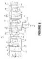
- FIG. 5is a schematic view of an alternative embodiment of the primary coil array driven by two coherent RF sources which have a 90° phase difference, showing the interaction between the primary induction coils of the primary unit and the receiving coil of the secondary unit in a simplified single primary coil array system for illustration purpose in accordance with one embodiment;
- FIG. 6is a schematic view of an embodiment of a two-dimensional primary coil array that is conceptually identical to that of FIG. 4 in accordance with one embodiment
- FIG. 7is a schematic view of an alternative embodiment of a two-dimensional primary coil array that is conceptually identical to that of FIG. 5 in accordance with one embodiment
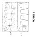
- FIGS. 8 a and bshows the magnetic fields for a linear array of five coils and the total magnetic field when all five coils are energized in phase by currents of equal amount in accordance with one embodiment
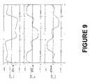
- FIG. 9displays a time sequence of magnetic field intensity to depict the traveling wave nature of the magnetic field excited by a long linear array of coils driven by the circuit shown in FIG. 5 in accordance with one embodiment
- FIG. 10shows the magnetic fields excited by a long linear array of primary coils at various times in accordance with one embodiment
- FIG. 11displays a time sequence of magnetic field intensity distribution to depict the traveling wave nature of the magnetic field excited by a large two dimensional array of coils driven by a circuit which is a two dimensional generalization of the circuit shown in FIG. 5 in accordance with one embodiment
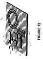
- FIG. 12is an isometric view of the secondary coil and circuit elements in the device adapter in accordance with one embodiment
- FIG. 13is a more detailed schematic view of the secondary coil and circuit elements in the device adapter in accordance with one embodiment
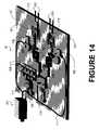
- FIG. 14is an isometric view of the RF generating module in the primary unit which generates two pairs of RF signals whose phases are 90 degrees apart in accordance with one embodiment
- FIG. 15is a more detailed schematic view of the RF generating module in the primary unit which generates two sets of RF signals which are 90 degrees apart in their respective phases in accordance with one embodiment
- FIG. 16shows a power factor correction subsystem for the class E amplifier module depicted in FIG. 15 in accordance with one embodiment.
- FIG. 1shows an isometric view, of a system of one embodiment invention during the process of wireless power transfer between a primary unit 20 and a secondary unit 30 .
- the primary unitconverts the DC power supplied by a conventional DC power supply 10 connected to an AC outlet 11 to a multitude of radio frequency oscillations.
- the various RF oscillationscan be of different RF frequencies, or they could all have the same frequency.
- the RF signalsare used to drive a set of primary coil arrays which are in general two dimensional in nature to generate inductive magnetic field above a substantially laminar surface 27 in which the primary coils 21 are embedded.
- the RF poweris transferred from the primary unit 20 to the secondary unit 30 by a RF cable 2 .
- the transferred RF poweris subsequently conditioned and rectified by the rectification circuit within the secondary unit 30 into a regulated DC power with a substantially constant voltage.
- the regulated DC poweris then used to power the device to perform such tasks as charging a secondary battery, or to be used directly by the device to power its electronics, etc.
- FIG. 2depicts an isometric view of a single array of inductive field coils 21 of the primary unit 20 together with a single coil 31 of the secondary unit 30 . It also illustrates the localization of the inductive field when the secondary coil 31 is brought close to the primary unit 20 (see the
- the self-induced localization of the inductive magnetic field of the primary unitarises from both the local resonance nature of the primary RF circuit, and from the adaptive circuitry that resides in the secondary unit 30 .
- the primary unithas a local parallel LC (inductance 21 -capacitance 22 ) balanced architecture to present a large primary load impedance to the RF power supply.
- the parallel LC impedancedecreases drastically to allow primary RF load current to flow into the local region.
- the resonance circuitry within the secondary unit 30couples to the local LC circuit of the primary unit 20 , and together, they form a new local resonance substructure.
- the secondary unit 30In order for the new local resonance substructure to tune in to the applied RF frequency, the secondary unit 30 must adaptively adjust its own self impedance to pull the resonance in.
- the need of an adaptive component in the secondary unit 30also means that it would be nearly impossible for any incompatible electronic device or a foreign object such as a metal bar, low reluctance magnetic material, or saline water to shift the local resonance enough to cause even a minute amount of power transfer. This greatly contributes to the safety of the present invention.
- FIG. 3is an isometric view of the primary unit 20 which comprises a two-dimensional array of primary coils 21 and attendant matching capacitors 22 as well as the power rails 29 for connecting the primary coils 21 and capacitors 22 to the primary RF power supply 10 .
- the primary coils 21are arranged in groups such that coils 21 from one group do not have strong coupling to coils 21 from another group because of the way each group is driven by the RF source, and neighboring coils 21 from the same group likewise are only weakly coupled because of the physical and geometrical constraints.
- Each compensating capacitor 22is placed in such a way that it can match the impedance of either a single primary coil 21 or a set of neighboring primary coils 21 to form a local parallel LC network.
- the LC networkexhibits nearly infinite impedance to the RF source, hence the primary load current through such network is normally blocked provided that all the local LC networks are tuned to the primary driving frequency. Therefore, if no secondary unit 30 is placed in the vicinity of such a network, the amount of load current flowing through it is at its minimum.
- the parallel LC resonance frequencyis shifted away from the driving frequency of the RF source 10 , which, in turns, causes the effective local LC impedance to decrease sufficiently to enable the load current to flow into the local LC network.
- the receiving coil in the secondary unit 30likewise has a compensating capacitor 32 in parallel with the receiving induction coil 31 .
- the increase in the local load current in turnsresults in the increase in the local magnetic field intensity which is shown in Graph 410 .
- the compensating capacitor 32 in the secondary unit 30is electronically adjustable. By varying the compensating capacitance of the secondary unit 30 , the resonance frequency of the combined local resonant network can be changed.
- FIG. 4is a schematic view showing the interaction between the primary induction coils 21 of the primary unit 20 and the receiving coil 31 of the secondary unit 30 in a simplified single primary coil array system for illustration purpose.
- the primary unit 20comprises a linear array of parallel LC networks all connected in parallel by the two RF feed rails 29 .
- the number of matching capacitors 22can be reduced by using one capacitor 22 to balance the load impedance of several neighboring inductive coils 21 .
- a single capacitor 22can be used to balance the entire primary coil array. The last case corresponds to a global impedance compensating scheme.
- the secondary unit 30comprises a receiving coil 31 in parallel with a matching capacitor 32 .
- the device that the secondary unit 30 is attached tois simplistically represented by a resistive load 33 in series with the parallel LC network formed by the receiving coil 31 and the matching capacitor 32 .
- the variable nature of the capacitor 32is indicated by the arrow across the capacitor symbol 32 .
- the resonance enhanced couplingdrastically altered the local load impedance of the combined network, which in turns shifts the primary local parallel LC resonance away from the operating frequency of the primary RF source 10 .
- the resonant couplingintroduces additional complex zeros and poles of the effective primary load impedance.
- the additional zeros and polesare all clustered together around the original resonance frequency which is taken to be the operating frequency of the primary unit 20 .
- the dominant zero of the combined local networkcan be tuned to the driving frequency of the primary unit 20 , which in turns varies the magnitude of the RF voltage across the secondary load 33 . This makes it possible to regulate the load voltage of the secondary unit 30 using a feedback control scheme.
- the feedback control loopcontinuously monitors the output voltage (usually the rectified DC voltage after the rectification stage that is needed to convert the RF power into DC power to power an electronic device, instead of the un-rectified RF voltage) and compares it to a reference voltage.
- the deviation of the output voltage from the reference voltageis the error signal which is fed to a controller.
- the controlleroutput a control signal which adjusts the capacitance value of the secondary RF matching capacitor 32 to tune the resonance frequency of the combined local resonance network either toward or away from the primary operating frequency in order to bring the output voltage close to the reference voltage.
- FIG. 5is a schematic view of an alternative embodiment of the primary coil array driven by two coherent RF sources 10 which have a 900 phase difference, showing the interaction between the primary induction coils 21 of the primary unit 20 and the receiving coil 31 of the secondary unit 30 in a simplified single primary coil array system for the purpose of elucidating the innovative concepts.
- This alternative embodimentovercomes a serious problem that arises from the way primary coils 21 are driven in the previous embodiment as described in FIG. 4 . In the previous RF driving arrangement, the coils are all driven in phase. Now the nature of the magnetic field generation by the individual primary coil 21 is such that the axial component of the magnetic field changes sign as it crosses from the interior of the coil 21 to the exterior through the coil boundary.
- the highly non-uniform magnetic field distributionis clearly one drawback of the same-phase driving geometry since this would implies that the magnetic field strength at the maximum point will be excessively high if the magnetic field minimum has to be above a certain threshold value in order to provide effective inductive power transfer over the entire active area of the primary surface 27 . And since the field strength reduction at the center of the coil array depends strongly on the number and sizes of the primary coils 21 , the ability to scale up to larger primary surface area is severely hampered.
- the inductive coilis made up of wire or trace of finite physical dimensions, and wires or traces between two adjacent coils 21 a and 21 b need to have a finite separation distance
- the magnetic field between two adjacent coils 21 a and 21 bactually can become negative, i.e. point in a direction which is the reverse of the direction of the main magnetic field.
- the magnetic field generated by the coil 21varies in strength in inverse proportionality to the distance between it and the wire or trace that carries the RF current, the magnitude of such reverse magnetic field can be rather large.
- the upshot of thisis that for certain small size secondary receiving coils 31 , the inductive coupling can actually go to zero. This occurs when there the total magnetic flux that is enclosed by the secondary coil 31 becomes zero as there are equal amount of positive and negative magnetic fields passing through the secondary coil 31 when the secondary coil 31 is positioned right along the border between the main field region and the reverse field region.
- coil-capacitance network 100is driven with an in-phase RF driver.
- Coil-capacitance network 101is driven with a 900 quadrature phase driver.
- Coil-capacitance network 102is driven by the same in-phase driver as coil-capacitance network 100 but in reverse, and coil-capacitance network 103 is driven by the quadrature phase driver in reverse.
- Coil-capacitance networks 104 , 105 , 106 and 107 , etc.are driven in turns by the same phase sequence over and over again until there is no more coil left.
- any two nearest coilsare separate roughly by the diameter of one primary coil 21 , assuming all coils 21 are equal in size. Due to the fact that the stray return magnetic field diminishes in strength fairly quickly away from the coil, the two nearest coils 21 c and 21 d within the same subgroup will have almost negligible mutual inductive couplings because of the physical separation. Adjacent coil coupling is also drastically reduced by virtual of the fact that tow adjacent coils 21 c and 21 e belong to different subgroups. And except at the edges of the primary array, a coil belonging to one subgroup, such as 21 e is always flanked by two coils belonging to the other subgroup, such as 21 c and 21 d .
- Coil-capacitance networks 102 , 103 and 104for example; Coil-capacitance networks 102 and 104 are driven 1800 out of phase, hence the negative mutual inductance from 102 to 103 is substantially canceled by the positive mutual inductance from 104 to 103 .
- 103is essentially uncoupled from the subgroup that coil-capacitance networks 102 and 104 belong to.
- the 900 driving geometry by and largedecouples the coils 21 from one another. This drastically diminishes the non-uniformity of the magnetic field except near the edge of the primary active surface. It also makes scaling up to larger surface a trivial task because of the substantially uncoupled nature of the primary coils 21 .
- FIG. 9 and FIG. 10describe the issue of coupling uniformity further.
- FIG. 6is a schematic view of an embodiment of a two-dimensional primary coil array that is conceptually identical to that of FIG. 4 .
- all primary coils 21are driven exactly in phase. So it suffers from the same ills as in FIG. 4 , namely, it has strong coupling non-uniformity, is difficult to scale up, and has magnetic field null as well as field reversal regions which makes effective contact-less power transfer impossible in those areas.
- the existence of dead spots in the active area of the primary surface 27is a serious drawback which will impede the usability of the system and limit its acceptance.
- One possible way of removing the dead spacesis to introduce another array of coils 21 underneath the first coil array.
- the second arrayis offset from the first array so that its own dead spots do not directly overlap with those of the first array.
- the second arraycan be driven by an independent RF power source 10 which has no fixed phase relationship with the RF source 10 for the first array.
- the second arraycan be driven 900 out of phase from the first one.
- the dead areasusually form long and narrow contours, hence some dead areas created by the original array and those created by the overlay array may still overlap. It is possible to design an overlay array network such that there are no overlapping dead spaces.
- the introduction of the overlay arrayalso increases the overall thickness as well as the system complexity of the primary unit 20 .
- the coils 21 of the stacked arraysare in the shape of a dense spiral formed on a layer of printed circuit board, then the amount of copper on the top array may well prevent the inductive field generated by the lower array from reaching the top surface, and vice versa.
- the introduction of an overlay arraymitigates, but does not solve the coupling non-uniformity problem.
- FIG. 7is a schematic view of an embodiment of a two-dimensional primary coil array that is conceptually identical to that of FIG. 5 .
- the primary coils 21are again divided into two groups in a checkerboard fashion. All physically adjacent coils are driven 900 out-of-phase and any two coils which are one coil apart and therefore belong to the same subgroup are driven 1800 out-of-phase.
- the same argument for the independence of primary coils 21 that applied to the simplified one dimensional array in FIG. 5still applies here.
- the mutual inductances between two nearest coils that belong to the same subgroupstill remains small although they are larger than those in the one dimensional case since the two coils are actually right next to each other along the diagonal.
- the coils 21 from the two subgroupshave substantially no coupling between them because each interior coil from one subgroup is surrounded by four coils from the other subgroup whose net induction flux through the center coil is ideally zero.
- the two-dimensional primary coil arraycan also be driven by other multi-phase scheme such as a 6-phase drive.
- a 6-phase driveAlthough for such drives, the independence of coils is no longer guaranteed.
- the larger mutual inductances among the coils 21make it harder for the drivers to maintain their phase relationships because of the mutual couplings.
- the added complexity of the higher phased drivesalso leads to greater cost.
- the chief advantage of higher phased drive schemesis the increased uniformity of the inductive magnetic field.
- FIG. 8 ashows the magnetic fields 261 , 262 , 263 , 264 , 265 for an array of five coils and the total magnetic field when all five coils are energized in phase by currents of equal amount.
- the magnetic field strengthis the strongest immediately above the current carrying conductor that constitute the coil, and it dips to a minimum at the center of the coil.
- the perpendicular component of the magnetic fieldchanges its sign as it crosses the outer boundary of the coil.
- the field reversal behavioris evident from the large negative dip just outside the coil in FIG. 8 a . It can be seen from the graph that the field reversal behavior is significant only for up to a distance equal to about one diameter of the coil.
- the resultant magnetic field 266is the sum of all the magnetic field generated by the five coils. Since the currents in adjacent conductors from different coils tend to cancel out, the five coils sum to an equivalent of one large coil.
- the magnetic field distribution 266can be seen to be much lower in strength with a pronounced dip in the center of the equivalent large coil.
- the large overlap in magnetic field distribution between adjacent coilsmeans that they will have a very large mutual inductance, and the field reversal also implies that the mutual inductive coupling between the two coils will be negative. Because of the large mutual coupling between adjacent coils, it is no longer possible to treat the individual coils as independent. Hence, for example, the total inductance of two adjacent coils driven in parallel and in phase is not half of the inductance of a single coil, but is a lot less owning to the large negative mutual coupling between the two coils. This makes it difficult to use the design for a smaller version of the primary unit to design a scaled up version since all the inductances have to be recalculated. Furthermore, in the scaled up version, more turns are needed to compensate for the strong mutual cancellation of the magnetic field.
- FIG. 8 bdepicts the summation field 267 of the same five coils except that any two adjacent coils are separated by 1 ⁇ 5th the coil diameter. The rather pronounced negative peaks are the result of the overlap of the negative peaks from adjacent coils.
- the coilsoften take the shape of a spiral, comprising a series of turns having substantially linear sections. Those kinds of coils are often constructed using printed circuit board (PCB) technique. Under certain conditions, a plurality of such coils can also create large reverse field regions when they are driven in phase. The mere presence of field reversal regions is in itself not a significant issue since the direction, or the sign, of the magnetic field is an oscillating function of time; hence the sign of the magnetic field at any particular instant is unimportant. However, the very existence of the reverse field implies that there are zero field contours which are the borders between the normal field regions and the reverse field regions.
- a secondary coil 31 placed at or around one of the field nullswill see both positive magnetic flux and negative magnetic flux which approximately cancel each other. Since the magnetic coupling between the primary coils 21 and the secondary coil 31 is directly proportional to the amount of magnetic flux that is enclosed by the secondary coil 31 , the cancellation of the magnetic flux significantly reduces the coupling and therefore the power transfer.
- Multi-phase driving of the primary coilsaddresses both the field reversal problem and the scalability problem.
- FIG. 9which displays a time sequence 271 , 272 , 273 of magnetic field intensity to depict the traveling wave nature of the magnetic field excited by a long linear array of coils driven by the circuit shown in FIG. 5 .
- FIG. 10shows the magnetic fields 391 , 392 , 393 , 394 , 395 excited by a long linear array of primary coils 21 at various times, in which the complete absence of magnetic null is evident.
- a multi-phase driving of the primary coil arrayis similar in nature to the technique used in driving a phased array antenna.
- an N-phase drivewhere N is a large number, will produce a magnetic field distribution which is close to a traveling sinusoidal waveform.
- Nis usually limited to a small to moderate number, since a large N would entail the use of a large number of costly phase shifters.
- the minimum Nis dictated by Nyquist Sampling Theorem.
- the 4-phased drive sequence depicted in FIG. 9clearly has an appearance of a highly distorted traveling sine wave. Due to the distorted nature of the traveling wave profile, the RMS (root-mean-square) magnetic field strength is not strictly uniform, as it would if the profile were truly sinusoidal.
- the calculated RMS variation of the magnetic field strength for the sequence depicted in FIG. 10is about ⁇ 22%.
- a more relevant measure of the field non-uniformityis to use the average field intensity of the computed magnetic field over a small aperture to calculate the RMS variation.
- the computed RMS variationis reduced to ⁇ 13%.
- a similar computationis done for a 6-phased drive example, and the aperture averaged RMS variation is only ⁇ 6%.
- the superior RMS variation figureis tempered by the higher mutual coupling among coil elements which makes phased driving more difficult and costly.
- FIG. 11displays a time sequence 491 , 492 , 493 , 494 of magnetic field intensity distribution that shows the traveling wave nature of the magnetic field excited by a two dimensional array of primary coils 21 driven by the circuit depicted in FIG. 7 .
- the two dimensional arrayhas roughly one and a half times the RMS variation of its one-dimensional counterpart, or around ⁇ 20% for a 4-phased driving scheme while the 6-phased scheme has about ⁇ 10%.
- bore sight directionis determined by the apparent phase velocity of the phased array elements. For example, when all the array elements are in phase, the apparent phase velocity becomes infinity, then it follows that the bore sight direction is the normal direction to the plane of the phased array (assuming planar phased array). When the apparent phase velocity is twice the speed of light, the bore sight direction is 300 from normal. In general, the deviation of the bore sight direction from normal is simply the arc-cosine of the ratio between the speed of light and the apparent phased speed of the array radiating elements.
- the apparent phase velocity of the radiating elementsshould never be lower than the speed of light.
- the apparent phase speed of the diagonal traveling waveshould be much smaller than the speed of light.
- the array pitchwhich is roughly the diameter of a single coil, is 1 ⁇ 4th the apparent phase wavelength, hence the apparent phase speed is the speed of light divided by 4 times the vacuum wavelength of the electromagnetic wave oscillating at the RF frequency and then by the array pitch.
- the RF frequencyis taken to be 30 MHz
- the array pitch of the primary unitis assumed to be 10 cm, then the apparent phase speed is just 4% of the speed of light.
- the primary array driven by a 4-phased RF driving techniquedoes not radiate.
- the single phase drive techniqueproduces an apparent phase speed which is equal to infinity; hence RF radiation is not precluded.
- the active area of the primary unitis typically much smaller than the RF wavelength, the level of RF radiation is still quite small since the primary unit behaves like a very poor antenna with negative antenna gain.
- FIG. 12is an isometric view of an exemplary embodiment of the secondary coil 31 and circuit elements in the device adapter.
- the secondary unit 30comprises a spiral shaped PCB trace coil as the receiving coil 31 , a main capacitor 32 a in parallel connection with the receiving coil 31 , and a bank of switched capacitors 32 b which are also in parallel with the main capacitor 32 a to form a variable and electronically adjustable capacitance, an impedance matching network 37 a , a full bridge rectifier 37 b , output capacitors 37 c that smoothes out output voltage ripple, a feedback voltage controller 34 to regulate the DC output voltage even as the inductive coupling between the secondary unit 30 and the primary surface 27 is constantly changing.
- the output capacitor 37 calso serves as the storage capacitor which accumulates energy to power the feedback controller during initial startup.
- the variable capacitor 32 of the secondary unit 30is still at its default value and the rectified DC voltage is still unregulated, the unregulated DC current starts charging the storage capacitor 37 c until 37 c reaches a voltage level that is high enough to turn the controller 34 on.
- the feedback controller 34is turned on, it starts to regulate the voltage by comparing the voltage of the storage capacitor 37 c and a reference voltage and takes the difference which is used as an error signal to control the variable capacitor.
- the capacitance adjustmentcauses the resonant circuit of the secondary unit 30 to tune in to the RF driving frequency of the primary unit 20 until the voltage reaches the reference voltage value.
- the controller 34can also compensate for any change in magnetic coupling or device load variation by tuning the secondary resonant circuit in or out of the primary RF driving frequency through continuous output voltage monitoring and capacitance adjustment.
- the ability of the secondary unit 30 to regulate its output voltageis advantageous in many situations where the device to which the secondary unit 30 is attached requires a regulated voltage to power it.
- Examples of devices that require regulated powerare mobile phones, personal digital assistants, laptop computers, MP3 players, ipods, digital cameras and camcorders, radios, portable game consoles or players, etc.
- a regulated switched mode power supplywhose output voltage and current are specifically designed for its use.
- the need of a dedicated DC power supplyis a major inconvenience for an end user who may carry a multitude of electronic devices with him or her and each device requires a different power supply.
- each devicehas a secondary unit 30 which can receive power from the primary unit 20 and convert it to whatever the voltage the device needs.
- the output voltage from the secondary unit 30is unregulated, it may need a linear voltage regulator if the power need of the device is small or a DC-DC converter if more efficient voltage regulation is required.
- the secondary unit 30 of the present inventioncan supply regulated voltage to the device, the need to have a separate voltage regulation device is obviated, making the conversion from the conventional power supply to the contactless one of the present invention painless.
- a DC current monitoring elementsuch as a series current sense resistor, or a current mirrored sense resistor when MOSFETs are used in the full bridge rectifier section 37 b , it would be possible to program the feedback controller 34 to control both the voltage and current to behave like a lithium ion/polymer charger with little or no additional cost.
- This specific embodiment of the secondary unit 30can also be profitably employed to construct a universal adapter for portable devices.
- Modern electronic devicesare designed with a lot of built-in protection mechanisms, including over-voltage protection, under-voltage protection, over-current protection, etc. If such a device is connected to a variable voltage power supply, it would block the supply voltage until the supply voltage exceeds a lower voltage threshold. Once the supply voltage has the right value, the device's power interface module will connect the device's power unit to the power supply. During the operation, if the supply voltage spikes to a value that exceeds the threshold for over-voltage protection, the device's power interface module immediately disconnect the power from the power supply.
- the deviceif the supply voltage dips to a value that is below a certain threshold, which may or may not be the same as the initial threshold, then the device also disconnect itself from the power supply, until the supply voltage returns to its normal range.
- a certain thresholdwhich may or may not be the same as the initial threshold
- the controller 34 of the secondary unit 30monitors the device current to determine whether the connection has been made. When the controller has detected the rise in output current beyond a certain current threshold, it determines that the connection has been made, and the voltage scanning stops.
- the controlleralso imposes a strict current limit to prevent inadvertent over voltage situation which might damage the device if it is not equipped with over-voltage protection. This may occur when the device in question is in a standby mode and does not consume enough current for the feedback controller to determine whether the device power connection has been made, in which case the controller 34 will decide that the voltage is not right and proceeds to step up to another voltage.
- the controller 34can detect fault conditions to determine whether over-voltage fault has occurred since under normal conditions the device's power interface module would insert a hysteresis time delay before connecting the power supply to the device, hence if that time delay is not there, then an over-voltage fault is indicated. Whenever a fault occurs, the controller 34 can reset the process and start the voltage scan sequence all over again until the power connection has been made without triggering a fault.
- FIG. 13A more detailed schematic view of the circuit elements in the device adapter is presented in FIG. 13 .
- the proportional, differential, and integral (PID) controller 34 amonitors the output voltage after the storage/smoothing capacitor 37 c and compares it to a reference voltage.
- the value of the bias capacitor 32 ais selected in such a way that, when it is coupled to the secondary receiving coil 31 , the combined LC network resonates with the primary RF driving frequency in the absence of any magnetic coupling with the primary unit 21 in conjunction with the receiving coil 31 .
- This choice of the bias capacitance 32 aalso ensures that even without any further adjustment of the parallel capacitance, the RF voltage induced by the primary coils 21 when the secondary unit 30 is in magnetic coupling with the primary unit 20 is sufficient to power the PID controller 34 . Furthermore, the nature of the coupling between the secondary 30 and the primary unit 20 is such that it tends to slightly raise the resonance frequency, which means that there needs to be additional parallel capacitance in order to restore the resonance to its original value so that it can stay matched with the RF driving frequency. This capacitance correction is provided by a bank of switched capacitors 32 b shown in FIG. 13 .
- the four capacitors 32 bare selected to have values which are powers of 2 of the smallest capacitance. So for example, if the smallest capacitance is 100 pF, then the other three capacitances are 200 pF, 400 pF and 800 pF. Each capacitor is in series with a MOSFET switch which can be turned on to enable the capacitor it is directly connected to, or to turn off to disable the capacitor.
- the switched capacitor bank 32 bcan provide 24 or 16 different capacitance values which are more or less linearly distributed with values from 0 pF to 1,500 pF.
- the capacitance valuesare not precise because of the inherent variation of stock capacitors as well as the source drain capacitances of the MOSFETs.
- the source drain capacitance of the MOSFETis unimportant when the MOSFET is ON.
- MOSFETis OFF, the capacitor it is connected to is not completely disabled because of the source drain capacitance which is in series with the external capacitor.
- the source drain capacitance of the MODFETis not a constant, either, but depends on the source drain voltage. Hence it would be difficult to modify the capacitance values of the external capacitors to compensate for the added OFF capacitances caused by MOSFETs.
- the PID controller 34can control the capacitance of the capacitor bank 32 b simply by issuing a binary word.
- a 4-bit wordcan be used in the capacitor bank 32 b depicted in FIG. 13 to change the capacitance to a multiple of the smallest capacitance such that the integer multiple is simply the numerical value of the 4-bit word.
- the switched capacitor bank 32 bcan be considered to be a DA (digital-to-analog) converter which converts a binary word into an analog capacitance value.
- DAdigital-to-analog
- FIG. 14is an isometric view of one embodiment of the RF generating module in the primary unit 20 which generates two pairs of RF signals whose phases are 900, 1800, 2700, and 00, respectively.
- square wave generator 109 with crystal oscillator 110Shown are, square wave generator 109 with crystal oscillator 110 , a pair of current amplifiers 108 , a pair of transformers 107 to step down the voltage, a pair of power MOSFETs 151 for high-frequency power switching, a pair of chokes 106 and their attendant smoothing capacitors 105 to isolate the DC power supply from the switching noise and vice versa, a pair of source drain capacitors 131 to control switch timing, and a pair of series connected inductors 101 and capacitors 115 to provide series resonance circuits, and two pairs of output ports 102 , 103 , one pair 102 for the 00 and 1800 phases, and the other pair 103 for the 900 and 2700 phases.
- the inductors 131 and transformers 101 as well as the chokes 106have either ferrite cores or iron powder cores, depending on the RF frequency, or other suitable high permeability magnetic materials to provide sufficient inductance values without needing a large number of turns for the coils.
- the use of magnetic materials for the transformers 107 and inductors 101also reduces RF cross coupling due to the leakage inductive magnetic field. This is because the high permeability material can act as a guide for the magnetic flux since the magnetic field prefers to complete its loop through a low reluctance path which the magnetic material provides.
- metal mesh Faraday cageswhich are placed over critical components such as the square wave generator 109 , the current amplifiers 108 , all the transformers 107 and inductors 101 , etc. in order to provide RF shielding of unwanted inductive magnetic field. This can prevent, for example, the unwanted coupling between a transformer 107 and the square wave generator 109 . Since the square wave generator 109 is capable of generating only a small amount of RF current, even a relatively small interfering stray RF magnetic field can significantly distort the waveform, thereby creating a vicious positive feedback cycle, causing the RF generator 10 to become unstable.
- the power supplied by the RF moduleis transmitted to the primary coils 21 through RF waveguides 2 .
- the most common waveguidesare coax cables, not shown, which are lightweight, flexible, and have relatively low transmission loss.
- the RF poweris delivered to the individual coils simply via separate rails 29 .
- the primary surface 27is large, then the RF power would be more advantageously delivered via coplanar waveguides or their equivalent in order to minimize transmission loss, reflections, and radiation.
- Splittersare also needed in conjunction with the coplanar waveguides to allow the individual coils to tap the RF power delivered by the shared waveguides.
- FIG. 15is a more detailed schematic circuit diagram view of the RF generating module in the embodiment depicted in FIG. 14 .
- the square wave generator 109with a crystal oscillator 110 to provide a stable, precise frequency reference, generates two square wave signals that are 900 apart in phase. Each signal is passed through a current amplifier 108 and then a step down transformer 107 to boost its current.
- the current amplificationis needed because the power MOSFET switches 151 require large gate currents to switch at radio frequencies. Further current amplification is provided by the transformer pair 151 which steps down the drive voltages.
- the step down transformers 151also insulate the gate drive section from load variations and RF reflections further down stream, which reduces the destabilizing effect of the Miller capacitance.
- the section of circuit immediately after the transformer 107is a class E amplifier.
- the choke 106is used basically as a large flywheel which both insulates the DC power supply 191 from large high-frequency fluctuation and provides a constant current source to the rest of the class E circuitry.
- the series LC resonator 101 and 115provides a high “Q” environment to filter out higher harmonics and enhance the fundamental frequency to produce a substantially sinusoidal waveform at the output ports 102 and 103 . It is to be appreciated that a class D amplifier, or any other switched pulse amplifier design can be profitably employed to accomplish the RF generating function.
- Both class E and class D amplifiershave been known to have achieved power conversion efficiencies as high as 92% and up, far higher than the more traditional class AB or class C amplifiers which typically have below 50% power efficiencies.
- Switched pulse amplifiersare quite sensitive to load variations and load power reflections, which can be somewhat mitigated by Faraday shielding of magnetic components and gate current amplification.
- the power MOSFETs 151are switched only when there is a zero crossing for the source-drain current.
- the flywheel actions of the choke and the main inductorwill try to maintain the current during the switch transition, thereby creating large voltage spikes with high harmonic content which lowers the overall power efficiency as well as distorting the output waveform.
- the zero crossing timing of the source drain currentis a strong function of both the load and the reflected RF power when there is a load impedance mismatch.
- FIG. 16shows a PFC subsystem for the class E amplifier module depicted in FIG. 15 .
- Current and voltage sensors 181 , 182are used to measure the output current and voltage. The results of the measurement can provide information about equivalent load impedance, RMS voltage and current, and the harmonic content of the amplifier output.
- Another voltage sensor 184is employed to monitor the drain voltage of the MOSFET transistor 151 whose harmonic content gives a very good indication of whether the class E amplifier is operating efficiently or not. Those data are fed to the power management module 193 .
- the power management module 193sends control signals to voltage control module 192 , capacitance control module 195 and duty cycle control module 196 to adjust the voltage of the main power supply 191 to the amplifier, the capacitance of the source drain capacitor 131 , and the square wave generator 109 .
- the DC voltage controlis achieved by changing the reference voltage of the fly back controller within the switched mode power supply.
- the capacitance adjustmentis accomplished by an electronically switched capacitor bank 131 , and the duty cycle control is performed by a digital potentiometer. Because the control has multiple inputs and multiple outputs, or MIMO, standard feedback control schemes such as PID scheme would no longer work. More advanced control schemes such as fuzzy logic control, linear or recursive least mean square or artificial neural network controls are needed.
- the power management modulecan gradually learn to control its outputs to reduce the harmonic content at the source voltage.
- FIG. 12 through FIG. 16are for illustrative purpose, and are not meant to be comprehensive, nor are they intended to exclude other components or techniques which are similar in scope and can perform similar functions.
- the switched capacitor bankperforms the function of an electronically controlled capacitor, and as such, it can be replaced by other electronically controlled capacitors such as varactors, or by a micro-electro-mechanical system (MEMS) based thin film capacitor.
- MEMSmicro-electro-mechanical system
- Different sensors and control elementscan be substituted in FIG. 16 for the PFC without fundamentally altering the basic principle of adaptive power optimization of the RF power module.
- a switched mode DC power supplycan also be replaced by a large primary battery, or a fuel cell battery, in which case the control of the DC supply voltage may be inhibited, or a DC-DC converter may becomes necessary.
- the PID controller in the secondary unitmay be replaced by a hybrid scheme where the four most significant bits are exhaustively searched to find a coarse optimum, and a PID controller then takes over to perform an analog search.
- Another alternativeis to exhaustively search all eight bits periodically to find and track the optimum point.
- the output voltage or current of the secondary unitmay be unregulated, and the PID controller or its equivalent is only employed to pull in the resonance.
- the multi-phased RF driving techniques used to power the apparent traveling wave in the primary unitcould also be substituted by a single phase driver that relies on the inherent slow wave structure of the primary coil array to excite a slow traveling wave across the primary coil array.
- Another alternative embodimentis to use a random multi-phased driver where the fixed phase relationships are replaced by random phase relationships.
Landscapes
- Engineering & Computer Science (AREA)
- Power Engineering (AREA)
- Computer Networks & Wireless Communication (AREA)
- Physics & Mathematics (AREA)
- Life Sciences & Earth Sciences (AREA)
- Remote Sensing (AREA)
- Electromagnetism (AREA)
- Environmental & Geological Engineering (AREA)
- Geology (AREA)
- General Life Sciences & Earth Sciences (AREA)
- General Physics & Mathematics (AREA)
- Geophysics (AREA)
- Charge And Discharge Circuits For Batteries Or The Like (AREA)
- Current-Collector Devices For Electrically Propelled Vehicles (AREA)
Abstract
Description
Claims (25)
Priority Applications (3)
| Application Number | Priority Date | Filing Date | Title |
|---|---|---|---|
| US11/319,818US7521890B2 (en) | 2005-12-27 | 2005-12-27 | System and method for selective transfer of radio frequency power |
| PCT/US2006/049093WO2007076043A2 (en) | 2005-12-27 | 2006-12-20 | A system and method for contact free transfer of power |
| TW095148983ATW200742224A (en) | 2005-12-27 | 2006-12-26 | A system and method for contact free transfer of power |
Applications Claiming Priority (1)
| Application Number | Priority Date | Filing Date | Title |
|---|---|---|---|
| US11/319,818US7521890B2 (en) | 2005-12-27 | 2005-12-27 | System and method for selective transfer of radio frequency power |
Publications (2)
| Publication Number | Publication Date |
|---|---|
| US20070145830A1 US20070145830A1 (en) | 2007-06-28 |
| US7521890B2true US7521890B2 (en) | 2009-04-21 |
Family
ID=38192795
Family Applications (1)
| Application Number | Title | Priority Date | Filing Date |
|---|---|---|---|
| US11/319,818Expired - Fee RelatedUS7521890B2 (en) | 2005-12-27 | 2005-12-27 | System and method for selective transfer of radio frequency power |
Country Status (3)
| Country | Link |
|---|---|
| US (1) | US7521890B2 (en) |
| TW (1) | TW200742224A (en) |
| WO (1) | WO2007076043A2 (en) |
Cited By (173)
| Publication number | Priority date | Publication date | Assignee | Title |
|---|---|---|---|---|
| US20080055279A1 (en)* | 2006-08-31 | 2008-03-06 | Semiconductor Energy Laboratory Co., Ltd. | Electronic pen and electronic pen system |
| US20080150475A1 (en)* | 2006-12-26 | 2008-06-26 | Semiconductor Energy Laboratory Co., Ltd. | Semiconductor Device |
| US20080203816A1 (en)* | 2007-02-28 | 2008-08-28 | Sanyo Electric Co., Ltd. | Power supply apparatus |
| US20080211314A1 (en)* | 2007-03-01 | 2008-09-04 | Graco Children's Products Inc. | Juvenile Product Inductive Power Transfer |
| US20090008994A1 (en)* | 2007-07-03 | 2009-01-08 | David A Tonn | Inductive coupling method for remote powering of sensors |
| US20090079271A1 (en)* | 2007-09-26 | 2009-03-26 | Seiko Epson Corporation | Power transmission control device, power transmitting device, non-contact power transmission system, and secondary coil positioning method |
| US20090079270A1 (en)* | 2007-09-26 | 2009-03-26 | Seiko Epson Corporation | Structure having a power transmitting device |
| US20090174476A1 (en)* | 2006-03-31 | 2009-07-09 | Naoki Komatsu | Noise reduction circuit for canceling leakage signal |
| US20090237194A1 (en)* | 2006-09-18 | 2009-09-24 | Koninklijke Philips Electronics N. V. | Apparatus, a system and a method for enabling electromagnetic energy transfer |
| US20090284245A1 (en)* | 2008-05-13 | 2009-11-19 | Qualcomm Incorporated | Wireless power transfer for appliances and equipments |
| US20100033021A1 (en)* | 2008-08-05 | 2010-02-11 | Broadcom Corporation | Phased array wireless resonant power delivery system |
| US20100081483A1 (en)* | 2008-09-26 | 2010-04-01 | Manjirnath Chatterjee | Shield for use with a computing device that receives an inductive signal transmission |
| US20100081473A1 (en)* | 2008-09-26 | 2010-04-01 | Manjirnath Chatterjee | Orientation and presence detection for use in configuring operations of computing devices in docked environments |
| US20100081377A1 (en)* | 2008-09-26 | 2010-04-01 | Manjirnath Chatterjee | Magnetic latching mechanism for use in mating a mobile computing device to an accessory device |
| US20100121965A1 (en)* | 2008-11-12 | 2010-05-13 | Palm, Inc. | Protocol for Program during Startup Sequence |
| US20100123452A1 (en)* | 2008-11-17 | 2010-05-20 | Toyota Jidosha Kabushiki Kaisha | Power supply system and method of controlling power supply system |
| US20100131691A1 (en)* | 2008-09-26 | 2010-05-27 | Manjirnath Chatterjee | Extending device functionality amongst inductively linked devices |
| US20100146308A1 (en)* | 2008-09-26 | 2010-06-10 | Richard Gioscia | Portable power supply device for mobile computing devices |
| US20100172090A1 (en)* | 2009-01-05 | 2010-07-08 | Manjirnath Chatterjee | Interior connector scheme for accessorizing a mobile computing device with a removeable housing segment |
| US20100201533A1 (en)* | 2009-02-10 | 2010-08-12 | Qualcomm Incorporated | Conveying device information relating to wireless charging |
| US20100201189A1 (en)* | 2008-05-13 | 2010-08-12 | Qualcomm Incorporated | Wireless power transfer for vehicles |
| US20100219698A1 (en)* | 2007-09-25 | 2010-09-02 | Powermat Ltd. | Centrally controlled inductive power transmission platform |
| US20100259110A1 (en)* | 2008-09-27 | 2010-10-14 | Kurs Andre B | Resonator optimizations for wireless energy transfer |
| US20100259217A1 (en)* | 2009-04-08 | 2010-10-14 | Access Business Group International Llc | Selectable coil array |
| US20100301678A1 (en)* | 2009-05-28 | 2010-12-02 | Electronics And Telecommunication Research Institute | Electric device, wireless power transmission device, and power transmission method thereof |
| US20100301801A1 (en)* | 2009-05-27 | 2010-12-02 | Bayerische Motoren Werke Aktiengesellschaft | Device for Mechanically and Electrically Connecting a Portable, Battery-Operated Apparatus and Portable, Battery-Operated Apparatus |
| US20110022350A1 (en)* | 2009-07-21 | 2011-01-27 | Manjirnath Chatterjee | System for Detecting Orientation of Magnetically Coupled Devices |
| US20110018356A1 (en)* | 2009-07-21 | 2011-01-27 | Manjirnath Chatterjee | Power bridge circuit for bi-directional wireless power transmission |
| US20110037321A1 (en)* | 2009-07-21 | 2011-02-17 | Manjirnath Chatterjee | Power bridge circuit for bi-directional inductive signaling |
| US20110084652A1 (en)* | 2009-10-08 | 2011-04-14 | Etymotic Research Inc. | Magnetically Coupled Battery Charging System |
| US20110095618A1 (en)* | 2008-09-27 | 2011-04-28 | Schatz David A | Wireless energy transfer using repeater resonators |
| US20110106954A1 (en)* | 2008-09-26 | 2011-05-05 | Manjirnath Chatterjee | System and method for inductively pairing devices to share data or resources |
| US20110156640A1 (en)* | 2009-12-25 | 2011-06-30 | Mehran Moshfeghi | Method and apparatus for wirelessly transferring power and communicating with one or more slave devices |
| USD640976S1 (en) | 2008-08-28 | 2011-07-05 | Hewlett-Packard Development Company, L.P. | Support structure and/or cradle for a mobile computing device |
| US20110169338A1 (en)* | 2010-01-14 | 2011-07-14 | Sony Corporation | Power feeding device, power receiving device and wireless power feeding system |
| US20110234154A1 (en)* | 2010-03-23 | 2011-09-29 | Amir Navid | Video game controller charging system |
| US20110234019A1 (en)* | 2007-08-17 | 2011-09-29 | Tmms Co., Ltd. | Method and device for transporting, distributing and managing electrical energy by remote longitudinal coupling in near field between electric dipoles |
| US20110260808A1 (en)* | 2010-04-23 | 2011-10-27 | Renesas Electronics Corporation | Electronic component and signal transmission method using the electronic component |
| US20110267002A1 (en)* | 2006-09-29 | 2011-11-03 | Access Business Group International Llc | System and method for inductively charging a battery |
| US20110285830A1 (en)* | 2010-05-19 | 2011-11-24 | Samsung Electro-Mechanics Co., Ltd. | Stereoscopic Image Display Apparatus Capable Of Wirelessly Transmitting and Receiving Power |
| US20120007437A1 (en)* | 2007-08-28 | 2012-01-12 | Access Business Group International Llc | Inductive power supply |
| US8115635B2 (en) | 2005-02-08 | 2012-02-14 | Abbott Diabetes Care Inc. | RF tag on test strips, test strip vials and boxes |
| US20120062345A1 (en)* | 2008-09-27 | 2012-03-15 | Kurs Andre B | Low resistance electrical conductor |
| US20120086268A1 (en)* | 2010-10-08 | 2012-04-12 | Sony Corporation | Power feeder and power feeding system |
| US20120091951A1 (en)* | 2010-10-19 | 2012-04-19 | Sohn Hyun Yeo | Apparatus and method for displaying measured strength in wirelessly charging battery |
| US20120105044A1 (en)* | 2009-06-10 | 2012-05-03 | Braun Gmbh | Circuit Arrangement And Method For Inductive Energy Transfer |
| US20120146425A1 (en)* | 2010-12-14 | 2012-06-14 | Samsung Electro-Mechanics Co., Ltd. | Wireless power transmission/reception apparatus and method |
| US20120153739A1 (en)* | 2010-12-21 | 2012-06-21 | Cooper Emily B | Range adaptation mechanism for wireless power transfer |
| US20120184338A1 (en)* | 2008-09-27 | 2012-07-19 | Kesler Morris P | Integrated repeaters for cell phone applications |
| US20120248888A1 (en)* | 2008-09-27 | 2012-10-04 | Kesler Morris P | Wireless energy transfer with resonator arrays for medical applications |
| US20120248892A1 (en)* | 2009-08-07 | 2012-10-04 | Grant Anthony Covic | Inductive power transfer system |
| US20120262005A1 (en)* | 2006-03-21 | 2012-10-18 | Murata Manufacturing Co., Ltd. | Device for transporting energy by partial influence through a dielectric medium |
| US8292052B2 (en) | 2010-06-24 | 2012-10-23 | General Electric Company | Power transfer system and method |
| WO2012150293A1 (en) | 2011-05-03 | 2012-11-08 | Scholz Peter-Dominik | Arrangement and method for contactless energy transmission with a coupling-minimized matrix of planar transmission coils |
| US8395547B2 (en) | 2009-08-27 | 2013-03-12 | Hewlett-Packard Development Company, L.P. | Location tracking for mobile computing device |
| US20130162204A1 (en)* | 2011-12-21 | 2013-06-27 | Hanrim Postech Co., Ltd. | Apparatus for detecting signal and wireless power transmitting apparatus having the same |
| US20130169466A1 (en)* | 2010-08-25 | 2013-07-04 | Clairvoyant Technology Llc | Rf metal detector and electronic article surveillance system using same |
| US20130175877A1 (en)* | 2011-01-28 | 2013-07-11 | Panasonic Corporation | Power supplying module for contactless power supplying device, method for using power supplying module of contactless power supplying device, and method for manufacturing power supplying module of contactless power supplying device |
| USD687038S1 (en) | 2009-11-17 | 2013-07-30 | Palm, Inc. | Docking station for a computing device |
| US20130260842A1 (en)* | 2012-03-29 | 2013-10-03 | GM Global Technology Operations LLC | Inductive charger for providing radio frequency ("rf") signal to a portable electric device |
| US20130324039A1 (en)* | 2012-06-01 | 2013-12-05 | Kabushiki Kaisha Toshiba | Power transmitter, power receiver and power transmission and reception system |
| US20130324052A1 (en)* | 2012-06-01 | 2013-12-05 | Kabushiki Kaisha Toshiba | Wireless communication device and wireless communication system |
| US20140091755A1 (en)* | 2012-09-28 | 2014-04-03 | Broadcom Corporation | Wireless Power Transfer Adaptation Triggers |
| US20140103738A1 (en)* | 2008-09-27 | 2014-04-17 | Witricity Corporation | Tunable wireless energy transfer systems |
| US8712324B2 (en) | 2008-09-26 | 2014-04-29 | Qualcomm Incorporated | Inductive signal transfer system for computing devices |
| US8725330B2 (en) | 2010-06-02 | 2014-05-13 | Bryan Marc Failing | Increasing vehicle security |
| US20140145517A1 (en)* | 2011-07-20 | 2014-05-29 | Panasonic Corporation | Non-contact power supply system |
| US8755815B2 (en) | 2010-08-31 | 2014-06-17 | Qualcomm Incorporated | Use of wireless access point ID for position determination |
| US20140167676A1 (en)* | 2011-06-06 | 2014-06-19 | Robert Bosch Gmbh | Battery pack having a separate power supply device for a wireless communication device of the battery pack |
| US8760009B2 (en) | 2011-05-25 | 2014-06-24 | Samuel Gong | Wireless power source |
| US8772973B2 (en) | 2008-09-27 | 2014-07-08 | Witricity Corporation | Integrated resonator-shield structures |
| US8818523B2 (en) | 2012-04-25 | 2014-08-26 | Medtronic, Inc. | Recharge of an implantable device in the presence of other conductive objects |
| US8847548B2 (en) | 2008-09-27 | 2014-09-30 | Witricity Corporation | Wireless energy transfer for implantable devices |
| US8850045B2 (en) | 2008-09-26 | 2014-09-30 | Qualcomm Incorporated | System and method for linking and sharing resources amongst devices |
| US8868939B2 (en) | 2008-09-26 | 2014-10-21 | Qualcomm Incorporated | Portable power supply device with outlet connector |
| US8875086B2 (en) | 2011-11-04 | 2014-10-28 | Witricity Corporation | Wireless energy transfer modeling tool |
| US8901779B2 (en) | 2008-09-27 | 2014-12-02 | Witricity Corporation | Wireless energy transfer with resonator arrays for medical applications |
| US8901778B2 (en) | 2008-09-27 | 2014-12-02 | Witricity Corporation | Wireless energy transfer with variable size resonators for implanted medical devices |
| US8907531B2 (en) | 2008-09-27 | 2014-12-09 | Witricity Corporation | Wireless energy transfer with variable size resonators for medical applications |
| US8912687B2 (en) | 2008-09-27 | 2014-12-16 | Witricity Corporation | Secure wireless energy transfer for vehicle applications |
| US8922066B2 (en) | 2008-09-27 | 2014-12-30 | Witricity Corporation | Wireless energy transfer with multi resonator arrays for vehicle applications |
| US8933594B2 (en) | 2008-09-27 | 2015-01-13 | Witricity Corporation | Wireless energy transfer for vehicles |
| US8937408B2 (en) | 2008-09-27 | 2015-01-20 | Witricity Corporation | Wireless energy transfer for medical applications |
| US8946938B2 (en) | 2008-09-27 | 2015-02-03 | Witricity Corporation | Safety systems for wireless energy transfer in vehicle applications |
| US8947186B2 (en) | 2008-09-27 | 2015-02-03 | Witricity Corporation | Wireless energy transfer resonator thermal management |
| US8957549B2 (en) | 2008-09-27 | 2015-02-17 | Witricity Corporation | Tunable wireless energy transfer for in-vehicle applications |
| US8963488B2 (en) | 2008-09-27 | 2015-02-24 | Witricity Corporation | Position insensitive wireless charging |
| US20150084585A1 (en)* | 2013-09-26 | 2015-03-26 | The Charles Stark Draper Laboratory, Inc. | Smart implant battery charger |
| US20150091523A1 (en)* | 2013-10-02 | 2015-04-02 | Mediatek Singapore Pte. Ltd. | Wireless charger system that has variable power / adaptive load modulation |
| US9035499B2 (en) | 2008-09-27 | 2015-05-19 | Witricity Corporation | Wireless energy transfer for photovoltaic panels |
| US20150155128A1 (en)* | 2014-06-21 | 2015-06-04 | University Of Electronic Science And Technology Of China | Miniaturized all-metal slow-wave structure |
| US9065423B2 (en) | 2008-09-27 | 2015-06-23 | Witricity Corporation | Wireless energy distribution system |
| US9077188B2 (en) | 2012-03-15 | 2015-07-07 | Golba Llc | Method and system for a battery charging station utilizing multiple types of power transmitters for wireless battery charging |
| US20150207357A1 (en)* | 2014-01-23 | 2015-07-23 | Electronics And Telecommunications Research Institute | Wireless power transmission device, wireless power reception device and wireless power transmission system |
| US9093853B2 (en) | 2008-09-27 | 2015-07-28 | Witricity Corporation | Flexible resonator attachment |
| US9097544B2 (en) | 2009-08-27 | 2015-08-04 | Qualcomm Incorporated | Location tracking for mobile computing device |
| US9099919B2 (en) | 2011-05-09 | 2015-08-04 | The Hong Kong University Of Science And Technology | Single-inductor-multiple-output regulator with synchronized current mode hysteretic control |
| US9095729B2 (en) | 2007-06-01 | 2015-08-04 | Witricity Corporation | Wireless power harvesting and transmission with heterogeneous signals |
| US9105959B2 (en) | 2008-09-27 | 2015-08-11 | Witricity Corporation | Resonator enclosure |
| US9106203B2 (en) | 2008-09-27 | 2015-08-11 | Witricity Corporation | Secure wireless energy transfer in medical applications |
| US9118203B2 (en) | 2011-11-15 | 2015-08-25 | Qualcomm Incorporated | Systems and methods for induction charging with a closed magnetic loop |
| US9160203B2 (en) | 2008-09-27 | 2015-10-13 | Witricity Corporation | Wireless powered television |
| US9184595B2 (en) | 2008-09-27 | 2015-11-10 | Witricity Corporation | Wireless energy transfer in lossy environments |
| US9201457B1 (en) | 2001-05-18 | 2015-12-01 | Qualcomm Incorporated | Synchronizing and recharging a connector-less portable computer system |
| US20160020637A1 (en)* | 2014-07-15 | 2016-01-21 | Rf Micro Devices, Inc. | Wireless charging circuit |
| US9246336B2 (en) | 2008-09-27 | 2016-01-26 | Witricity Corporation | Resonator optimizations for wireless energy transfer |
| US9246349B2 (en) | 2010-12-27 | 2016-01-26 | Golba Llc | Method and system for wireless battery charging utilizing ultrasonic transducer array based beamforming |
| US9287607B2 (en) | 2012-07-31 | 2016-03-15 | Witricity Corporation | Resonator fine tuning |
| US9306635B2 (en) | 2012-01-26 | 2016-04-05 | Witricity Corporation | Wireless energy transfer with reduced fields |
| US9312924B2 (en) | 2009-02-10 | 2016-04-12 | Qualcomm Incorporated | Systems and methods relating to multi-dimensional wireless charging |
| US9318257B2 (en) | 2011-10-18 | 2016-04-19 | Witricity Corporation | Wireless energy transfer for packaging |
| US9318922B2 (en) | 2008-09-27 | 2016-04-19 | Witricity Corporation | Mechanically removable wireless power vehicle seat assembly |
| US9343922B2 (en) | 2012-06-27 | 2016-05-17 | Witricity Corporation | Wireless energy transfer for rechargeable batteries |
| US9369182B2 (en) | 2008-09-27 | 2016-06-14 | Witricity Corporation | Wireless energy transfer using variable size resonators and system monitoring |
| US9384885B2 (en) | 2011-08-04 | 2016-07-05 | Witricity Corporation | Tunable wireless power architectures |
| US9396867B2 (en) | 2008-09-27 | 2016-07-19 | Witricity Corporation | Integrated resonator-shield structures |
| US9404954B2 (en) | 2012-10-19 | 2016-08-02 | Witricity Corporation | Foreign object detection in wireless energy transfer systems |
| US9421388B2 (en) | 2007-06-01 | 2016-08-23 | Witricity Corporation | Power generation for implantable devices |
| US9431707B2 (en) | 2011-01-28 | 2016-08-30 | Samsung Electronics Co., Ltd. | Apparatus and method for wireless power transmission including a source resonator having a substantially uniform megnetic field |
| US9441939B2 (en) | 2010-08-25 | 2016-09-13 | Clairvoyant Technology Llc | System for object detection using radio frequency reflection |
| US9444520B2 (en) | 2008-09-27 | 2016-09-13 | Witricity Corporation | Wireless energy transfer converters |
| US9442172B2 (en) | 2011-09-09 | 2016-09-13 | Witricity Corporation | Foreign object detection in wireless energy transfer systems |
| US9449757B2 (en) | 2012-11-16 | 2016-09-20 | Witricity Corporation | Systems and methods for wireless power system with improved performance and/or ease of use |
| US9515494B2 (en) | 2008-09-27 | 2016-12-06 | Witricity Corporation | Wireless power system including impedance matching network |
| US9544683B2 (en) | 2008-09-27 | 2017-01-10 | Witricity Corporation | Wirelessly powered audio devices |
| US9583953B2 (en) | 2009-02-10 | 2017-02-28 | Qualcomm Incorporated | Wireless power transfer for portable enclosures |
| US9595378B2 (en) | 2012-09-19 | 2017-03-14 | Witricity Corporation | Resonator enclosure |
| US9602168B2 (en) | 2010-08-31 | 2017-03-21 | Witricity Corporation | Communication in wireless energy transfer systems |
| US9601266B2 (en) | 2008-09-27 | 2017-03-21 | Witricity Corporation | Multiple connected resonators with a single electronic circuit |
| US9601270B2 (en) | 2008-09-27 | 2017-03-21 | Witricity Corporation | Low AC resistance conductor designs |
| US20170093168A1 (en)* | 2015-09-24 | 2017-03-30 | Qualcomm Incorporated | Wireless power transfer receiver having closed loop voltage control |
| US9697951B2 (en) | 2012-08-29 | 2017-07-04 | General Electric Company | Contactless power transfer system |
| US9749017B2 (en) | 2015-08-13 | 2017-08-29 | Golba Llc | Wireless charging system |
| US9744858B2 (en) | 2008-09-27 | 2017-08-29 | Witricity Corporation | System for wireless energy distribution in a vehicle |
| US9754718B2 (en) | 2008-09-27 | 2017-09-05 | Witricity Corporation | Resonator arrays for wireless energy transfer |
| US9780573B2 (en) | 2014-02-03 | 2017-10-03 | Witricity Corporation | Wirelessly charged battery system |
| US9837860B2 (en) | 2014-05-05 | 2017-12-05 | Witricity Corporation | Wireless power transmission systems for elevators |
| US9842688B2 (en) | 2014-07-08 | 2017-12-12 | Witricity Corporation | Resonator balancing in wireless power transfer systems |
| US9842687B2 (en) | 2014-04-17 | 2017-12-12 | Witricity Corporation | Wireless power transfer systems with shaped magnetic components |
| US9843217B2 (en) | 2015-01-05 | 2017-12-12 | Witricity Corporation | Wireless energy transfer for wearables |
| US9857821B2 (en) | 2013-08-14 | 2018-01-02 | Witricity Corporation | Wireless power transfer frequency adjustment |
| US9892849B2 (en) | 2014-04-17 | 2018-02-13 | Witricity Corporation | Wireless power transfer systems with shield openings |
| US9929721B2 (en) | 2015-10-14 | 2018-03-27 | Witricity Corporation | Phase and amplitude detection in wireless energy transfer systems |
| US9948145B2 (en) | 2011-07-08 | 2018-04-17 | Witricity Corporation | Wireless power transfer for a seat-vest-helmet system |
| US9952266B2 (en) | 2014-02-14 | 2018-04-24 | Witricity Corporation | Object detection for wireless energy transfer systems |
| US9954375B2 (en) | 2014-06-20 | 2018-04-24 | Witricity Corporation | Wireless power transfer systems for surfaces |
| KR101875974B1 (en)* | 2013-08-14 | 2018-07-06 | 엘지이노텍 주식회사 | A wireless power transmission apparatus and method thereof |
| US10018744B2 (en) | 2014-05-07 | 2018-07-10 | Witricity Corporation | Foreign object detection in wireless energy transfer systems |
| US10063110B2 (en) | 2015-10-19 | 2018-08-28 | Witricity Corporation | Foreign object detection in wireless energy transfer systems |
| US10063104B2 (en) | 2016-02-08 | 2018-08-28 | Witricity Corporation | PWM capacitor control |
| US10075019B2 (en) | 2015-11-20 | 2018-09-11 | Witricity Corporation | Voltage source isolation in wireless power transfer systems |
| US10083792B2 (en) | 2014-05-14 | 2018-09-25 | Qualcomm Incorporated | System, method and apparatus for reducing the height of bipolar transmitters and/or receivers in electric vehicle charging |
| US10112495B2 (en) | 2015-07-27 | 2018-10-30 | Ford Global Technologies, Llc | Vehicle wireless charging system including an inverter to control a voltage input to a vehicle power converter |
| US10141788B2 (en) | 2015-10-22 | 2018-11-27 | Witricity Corporation | Dynamic tuning in wireless energy transfer systems |
| US10248899B2 (en) | 2015-10-06 | 2019-04-02 | Witricity Corporation | RFID tag and transponder detection in wireless energy transfer systems |
| US10263473B2 (en) | 2016-02-02 | 2019-04-16 | Witricity Corporation | Controlling wireless power transfer systems |
| US10312744B2 (en)* | 2013-02-04 | 2019-06-04 | Ossia Inc. | Techniques for delivering pulsed wireless power |
| US10396586B1 (en)* | 2016-09-21 | 2019-08-27 | Marcellus Chen | Wireless charging and powering of electronic devices by multipurpose wireless transmitting devices |
| US10424976B2 (en) | 2011-09-12 | 2019-09-24 | Witricity Corporation | Reconfigurable control architectures and algorithms for electric vehicle wireless energy transfer systems |
| US10559970B2 (en) | 2014-09-16 | 2020-02-11 | Qorvo Us, Inc. | Method for wireless charging power control |
| US10574091B2 (en) | 2014-07-08 | 2020-02-25 | Witricity Corporation | Enclosures for high power wireless power transfer systems |
| US10819154B2 (en) | 2016-09-06 | 2020-10-27 | Apple Inc. | Inductive power transmitter |
| US10840713B2 (en)* | 2016-09-30 | 2020-11-17 | Transform Sr Brands Llc | Charger, charge indicator, and associated methods |
| US10922939B1 (en) | 2019-04-11 | 2021-02-16 | Nexite Ltd. | Information management system for tagged goods |
| US11031818B2 (en) | 2017-06-29 | 2021-06-08 | Witricity Corporation | Protection and control of wireless power systems |
| US20210286958A1 (en)* | 2020-03-12 | 2021-09-16 | Arm Limited | Protocol for allocation of power signal |
| US11296557B2 (en) | 2017-05-30 | 2022-04-05 | Wireless Advanced Vehicle Electrification, Llc | Single feed multi-pad wireless charging |
| US11462943B2 (en) | 2018-01-30 | 2022-10-04 | Wireless Advanced Vehicle Electrification, Llc | DC link charging of capacitor in a wireless power transfer pad |
| USRE49300E1 (en) | 2008-12-12 | 2022-11-15 | Ge Hybrid Technologies, Llc | Non-contact charging station with power transmission planar spiral core, non-contact power-receiving apparatus, and method for controlling the same |
| US11508225B2 (en) | 2021-01-11 | 2022-11-22 | Nexite Ltd. | Theft prevention for returned merchandise |
| US11551537B2 (en) | 2019-04-11 | 2023-01-10 | Nexite Ltd. | Wireless dual-mode identification tag |
| US11620485B2 (en) | 2020-06-10 | 2023-04-04 | Arm Limited | Device and/or method for adaptive computation |
| US11797928B2 (en) | 2021-12-13 | 2023-10-24 | Nexite Ltd. | Dual-antenna, four-armed identification tag |
Families Citing this family (161)
| Publication number | Priority date | Publication date | Assignee | Title |
|---|---|---|---|---|
| CN101860089B (en) | 2005-07-12 | 2013-02-06 | 麻省理工学院 | wireless non-radiative energy transfer |
| US7825543B2 (en)* | 2005-07-12 | 2010-11-02 | Massachusetts Institute Of Technology | Wireless energy transfer |
| US8447234B2 (en) | 2006-01-18 | 2013-05-21 | Qualcomm Incorporated | Method and system for powering an electronic device via a wireless link |
| US9130602B2 (en) | 2006-01-18 | 2015-09-08 | Qualcomm Incorporated | Method and apparatus for delivering energy to an electrical or electronic device via a wireless link |
| US11201500B2 (en)* | 2006-01-31 | 2021-12-14 | Mojo Mobility, Inc. | Efficiencies and flexibilities in inductive (wireless) charging |
| US7355150B2 (en)* | 2006-03-23 | 2008-04-08 | Access Business Group International Llc | Food preparation system with inductive power |
| US8482157B2 (en) | 2007-03-02 | 2013-07-09 | Qualcomm Incorporated | Increasing the Q factor of a resonator |
| US9774086B2 (en) | 2007-03-02 | 2017-09-26 | Qualcomm Incorporated | Wireless power apparatus and methods |
| US8378523B2 (en) | 2007-03-02 | 2013-02-19 | Qualcomm Incorporated | Transmitters and receivers for wireless energy transfer |
| EP2135359A4 (en)* | 2007-03-16 | 2011-07-27 | Lg Electronics Inc | Performing contactless applications in battery off mode |
| US9124120B2 (en) | 2007-06-11 | 2015-09-01 | Qualcomm Incorporated | Wireless power system and proximity effects |
| US20090001941A1 (en)* | 2007-06-29 | 2009-01-01 | Microsoft Corporation | Inductive Powering Surface for Powering Portable Devices |
| WO2009036405A1 (en) | 2007-09-13 | 2009-03-19 | Nigelpower, Llc | Maximizing power yield from wireless power magnetic resonators |
| KR101502248B1 (en)* | 2007-09-19 | 2015-03-12 | 퀄컴 인코포레이티드 | Maximizing power yield from wireless power magnetic resonators |
| JP5362733B2 (en) | 2007-10-11 | 2013-12-11 | クゥアルコム・インコーポレイテッド | Wireless power transfer using a magneto-mechanical system |
| US20090160261A1 (en)* | 2007-12-19 | 2009-06-25 | Nokia Corporation | Wireless energy transfer |
| US8884468B2 (en) | 2007-12-21 | 2014-11-11 | Access Business Group International Llc | Circuitry for inductive power transfer |
| US8338990B2 (en)* | 2008-03-13 | 2012-12-25 | Access Business Group International Llc | Inductive power supply system with multiple coil primary |
| US8629576B2 (en) | 2008-03-28 | 2014-01-14 | Qualcomm Incorporated | Tuning and gain control in electro-magnetic power systems |
| WO2009144542A1 (en)* | 2008-04-15 | 2009-12-03 | Toyota Jidosha Kabushiki Kaisha | Wireless energy transfer device |
| JP2009268181A (en)* | 2008-04-22 | 2009-11-12 | Olympus Corp | Energy supply apparatus |
| US20090273242A1 (en)* | 2008-05-05 | 2009-11-05 | Nigelpower, Llc | Wireless Delivery of power to a Fixed-Geometry power part |
| US20110050164A1 (en) | 2008-05-07 | 2011-03-03 | Afshin Partovi | System and methods for inductive charging, and improvements and uses thereof |
| CN102099958B (en)* | 2008-05-14 | 2013-12-25 | 麻省理工学院 | Wireless power transfer including interference enhancement |
| JP4725664B2 (en)* | 2008-06-25 | 2011-07-13 | セイコーエプソン株式会社 | Power transmission control device, power transmission device, power reception control device, power reception device, electronic device, power transmission control method, and power reception control method |
| WO2010022059A1 (en) | 2008-08-18 | 2010-02-25 | Austin Christopher B | Vehicular battery charger, charging system, and method |
| WO2010020895A2 (en)* | 2008-08-18 | 2010-02-25 | Nxp B.V. | A mobile device to control a charge pad system |
| US9473209B2 (en)* | 2008-08-20 | 2016-10-18 | Intel Corporation | Wireless power transfer apparatus and method thereof |
| US8299652B2 (en) | 2008-08-20 | 2012-10-30 | Intel Corporation | Wireless power transfer apparatus and method thereof |
| US8400017B2 (en) | 2008-09-27 | 2013-03-19 | Witricity Corporation | Wireless energy transfer for computer peripheral applications |
| US8461721B2 (en)* | 2008-09-27 | 2013-06-11 | Witricity Corporation | Wireless energy transfer using object positioning for low loss |
| US8587153B2 (en) | 2008-09-27 | 2013-11-19 | Witricity Corporation | Wireless energy transfer using high Q resonators for lighting applications |
| US8304935B2 (en) | 2008-09-27 | 2012-11-06 | Witricity Corporation | Wireless energy transfer using field shaping to reduce loss |
| US8410636B2 (en) | 2008-09-27 | 2013-04-02 | Witricity Corporation | Low AC resistance conductor designs |
| US8629578B2 (en) | 2008-09-27 | 2014-01-14 | Witricity Corporation | Wireless energy transfer systems |
| US8461722B2 (en) | 2008-09-27 | 2013-06-11 | Witricity Corporation | Wireless energy transfer using conducting surfaces to shape field and improve K |
| US8461720B2 (en) | 2008-09-27 | 2013-06-11 | Witricity Corporation | Wireless energy transfer using conducting surfaces to shape fields and reduce loss |
| US8669676B2 (en) | 2008-09-27 | 2014-03-11 | Witricity Corporation | Wireless energy transfer across variable distances using field shaping with magnetic materials to improve the coupling factor |
| US8487480B1 (en) | 2008-09-27 | 2013-07-16 | Witricity Corporation | Wireless energy transfer resonator kit |
| US8471410B2 (en) | 2008-09-27 | 2013-06-25 | Witricity Corporation | Wireless energy transfer over distance using field shaping to improve the coupling factor |
| US8476788B2 (en) | 2008-09-27 | 2013-07-02 | Witricity Corporation | Wireless energy transfer with high-Q resonators using field shaping to improve K |
| US8723366B2 (en) | 2008-09-27 | 2014-05-13 | Witricity Corporation | Wireless energy transfer resonator enclosures |
| EP3179640A1 (en) | 2008-09-27 | 2017-06-14 | WiTricity Corporation | Wireless energy transfer systems |
| US8686598B2 (en) | 2008-09-27 | 2014-04-01 | Witricity Corporation | Wireless energy transfer for supplying power and heat to a device |
| US8569914B2 (en) | 2008-09-27 | 2013-10-29 | Witricity Corporation | Wireless energy transfer using object positioning for improved k |
| US8692410B2 (en) | 2008-09-27 | 2014-04-08 | Witricity Corporation | Wireless energy transfer with frequency hopping |
| US8441154B2 (en) | 2008-09-27 | 2013-05-14 | Witricity Corporation | Multi-resonator wireless energy transfer for exterior lighting |
| US20140361627A1 (en)* | 2013-06-07 | 2014-12-11 | Witricity Corporation | Wireless energy transfer using variable size resonators and system monitoring |
| US8324759B2 (en) | 2008-09-27 | 2012-12-04 | Witricity Corporation | Wireless energy transfer using magnetic materials to shape field and reduce loss |
| US8466583B2 (en) | 2008-09-27 | 2013-06-18 | Witricity Corporation | Tunable wireless energy transfer for outdoor lighting applications |
| US8552592B2 (en) | 2008-09-27 | 2013-10-08 | Witricity Corporation | Wireless energy transfer with feedback control for lighting applications |
| US8692412B2 (en) | 2008-09-27 | 2014-04-08 | Witricity Corporation | Temperature compensation in a wireless transfer system |
| US8587155B2 (en) | 2008-09-27 | 2013-11-19 | Witricity Corporation | Wireless energy transfer using repeater resonators |
| US8362651B2 (en) | 2008-10-01 | 2013-01-29 | Massachusetts Institute Of Technology | Efficient near-field wireless energy transfer using adiabatic system variations |
| AU2010203795A1 (en) | 2009-01-06 | 2011-07-14 | Access Business Group International Llc | Wireless charging system with device power compliance |
| US11476566B2 (en) | 2009-03-09 | 2022-10-18 | Nucurrent, Inc. | Multi-layer-multi-turn structure for high efficiency wireless communication |
| US8686684B2 (en)* | 2009-03-27 | 2014-04-01 | Microsoft Corporation | Magnetic inductive charging with low far fields |
| US8536736B2 (en)* | 2009-04-03 | 2013-09-17 | International Business Machines Corporation | Wireless power infrastructure |
| US8655272B2 (en)* | 2009-07-07 | 2014-02-18 | Nokia Corporation | Wireless charging coil filtering |
| RU2548367C2 (en)* | 2009-07-13 | 2015-04-20 | Конинклейке Филипс Электроникс Н.В. | Energy inductive transmission |
| DE102009033236A1 (en) | 2009-07-14 | 2011-01-20 | Conductix-Wampfler Ag | Device for inductive transmission of electrical energy |
| DE102009033237A1 (en)* | 2009-07-14 | 2011-01-20 | Conductix-Wampfler Ag | Device for inductive transmission of electrical energy |
| USD611898S1 (en) | 2009-07-17 | 2010-03-16 | Lin Wei Yang | Induction charger |
| USD611899S1 (en) | 2009-07-31 | 2010-03-16 | Lin Wei Yang | Induction charger |
| USD611900S1 (en) | 2009-07-31 | 2010-03-16 | Lin Wei Yang | Induction charger |
| JP2011050140A (en)* | 2009-08-26 | 2011-03-10 | Sony Corp | Non-contact electric power feeding apparatus, non-contact power electric receiver receiving apparatus, non-contact electric power feeding method, non-contact electric power receiving method and non-contact electric power feeding system |
| US20110057606A1 (en)* | 2009-09-04 | 2011-03-10 | Nokia Corpation | Safety feature for wireless charger |
| US8928284B2 (en) | 2009-09-10 | 2015-01-06 | Qualcomm Incorporated | Variable wireless power transmission |
| KR101197579B1 (en)* | 2009-11-04 | 2012-11-06 | 한국전기연구원 | Space-adaptive Wireless Power Transmission System and Method using Resonance of Evanescent Waves |
| US8427101B2 (en)* | 2009-11-18 | 2013-04-23 | Nokia Corporation | Wireless energy repeater |
| JP5016069B2 (en) | 2010-01-12 | 2012-09-05 | トヨタ自動車株式会社 | Power transmission system and vehicle power supply device |
| JP6144195B2 (en)* | 2010-05-19 | 2017-07-12 | オークランド ユニサービシズ リミテッドAuckland Uniservices Limited | Inductive power transfer system primary track topology |
| EP2580837A2 (en) | 2010-06-10 | 2013-04-17 | Access Business Group International LLC | Coil configurations for inductive power transfer |
| WO2011156768A2 (en) | 2010-06-11 | 2011-12-15 | Mojo Mobility, Inc. | System for wireless power transfer that supports interoperability, and multi-pole magnets for use therewith |
| KR101782354B1 (en)* | 2010-08-30 | 2017-09-27 | 삼성전자주식회사 | Apparatus and method for resonant power transmission and resonant power reception |
| USD636333S1 (en)* | 2010-09-23 | 2011-04-19 | Witricity Corporation | Wireless power source |
| US11342777B2 (en) | 2011-01-18 | 2022-05-24 | Mojo Mobility, Inc. | Powering and/or charging with more than one protocol |
| US9118357B2 (en)* | 2011-02-17 | 2015-08-25 | Qualcomm Incorporated | Systems and methods for controlling output power of a wireless power transmitter |
| WO2012121371A1 (en)* | 2011-03-10 | 2012-09-13 | Necトーキン株式会社 | Power-receiving device and non-contact power transmission system using same |
| JP5447413B2 (en)* | 2011-03-16 | 2014-03-19 | 株式会社ダイフク | Secondary power receiving circuit for contactless power supply equipment |
| KR101246693B1 (en)* | 2011-03-23 | 2013-03-21 | 주식회사 한림포스텍 | Wireless power receiving device and power control method thereof |
| US9496081B2 (en) | 2011-04-08 | 2016-11-15 | Access Business Group International Llc | Counter wound inductive power supply |
| KR101896921B1 (en)* | 2011-05-17 | 2018-09-12 | 삼성전자주식회사 | Wireless power receiver and method for controlling thereof |
| US9492678B2 (en) | 2011-07-14 | 2016-11-15 | Cyberonics, Inc. | Far field radiative powering of implantable medical therapy delivery devices |
| US8989867B2 (en) | 2011-07-14 | 2015-03-24 | Cyberonics, Inc. | Implantable nerve wrap for nerve stimulation configured for far field radiative powering |
| US9675809B2 (en)* | 2011-07-14 | 2017-06-13 | Cyberonics, Inc. | Circuit, system and method for far-field radiative powering of an implantable medical device |
| KR101893104B1 (en)* | 2011-08-19 | 2018-08-31 | 삼성전자주식회사 | Wireless power receiver for controlling wireless power by using switch |
| EP2775590B1 (en)* | 2011-11-04 | 2018-07-11 | Panasonic Intellectual Property Management Co., Ltd. | Coil unit and contactless electric power transmission device |
| KR101813125B1 (en)* | 2011-11-18 | 2017-12-29 | 삼성전자주식회사 | Wireless power transmission system, method for power control of in wireless power transmission system using detecting parameter |
| KR101338654B1 (en)* | 2011-12-19 | 2013-12-06 | 엘지이노텍 주식회사 | Apparatus for transmitting wireless power, apparatus for receiving wireless power, system for transmitting wireless power and method for transmitting wireless power |
| BR112014014707A2 (en)* | 2011-12-22 | 2017-06-13 | Koninklijke Philips Nv | system for charging one or more target devices with a receptacle charger and method for controlling the loading of at least one target device positioned in a receptacle |
| WO2013103756A1 (en)* | 2012-01-06 | 2013-07-11 | Access Business Group International Llc | Wireless power receiver system |
| US10778045B2 (en)* | 2012-01-30 | 2020-09-15 | Triune Ip, Llc | Method and system of wireless power transfer foreign object detection |
| CN107370249B (en) | 2012-03-14 | 2020-06-09 | 索尼公司 | Power transmitting device and non-contact power supply system |
| JP2013192391A (en)* | 2012-03-14 | 2013-09-26 | Sony Corp | Detecting apparatus, power receiving apparatus, power transmitting apparatus, and contactless power supply system |
| JP5967989B2 (en) | 2012-03-14 | 2016-08-10 | ソニー株式会社 | Detecting device, power receiving device, power transmitting device, and non-contact power feeding system |
| US9522282B2 (en) | 2012-03-29 | 2016-12-20 | Cyberonics, Inc. | Powering multiple implantable medical therapy delivery devices using far field radiative powering at multiple frequencies |
| EP3264564A1 (en)* | 2012-05-04 | 2018-01-03 | DET International Holding Limited | Multiple resonant cells for inductive charging pads |
| KR101789195B1 (en)* | 2012-05-16 | 2017-10-26 | 한국전자통신연구원 | Resonance coupling wireless energy transfer receiver and transmistter |
| US9632969B2 (en)* | 2012-08-07 | 2017-04-25 | Google Inc. | Systems and methods for managing a wireless connection between a computing device and a peripheral module |
| GB201215152D0 (en) | 2012-08-24 | 2012-10-10 | Imp Innovations Ltd | Maximising DC to load efficiency for inductive power transfer |
| US9275791B2 (en) | 2012-08-31 | 2016-03-01 | Qualcomm Incorporated | Systems and methods for decoupling multiple wireless charging transmitters |
| US9666357B2 (en) | 2012-09-11 | 2017-05-30 | Qualcomm Incorporated | Apparatus system, and method for wirelessly receiving power using conductive structures |
| US9293251B2 (en) | 2012-10-11 | 2016-03-22 | Panasonic Intellectual Property Management Co., Ltd. | Method of exciting primary coils in contactless power supplying device and contactless power supplying device |
| TWI462424B (en)* | 2012-10-15 | 2014-11-21 | Panasonic Corp | Method of exciting primary coils in contactless power supply device and contactless power supply device |
| EP2953542A4 (en) | 2013-02-06 | 2016-10-05 | California Inst Of Techn | IMPLANTABLE AND MINIATURIZED ELECTROCHEMICAL SENSOR DEVICES |
| JP2014209813A (en)* | 2013-04-16 | 2014-11-06 | 日東電工株式会社 | Wireless power transmission device, heating control method of wireless power transmission device, and method of manufacturing wireless power transmission device |
| GB201321267D0 (en) | 2013-12-02 | 2014-01-15 | Imp Innovations Ltd | Inductive power transfer system |
| US9601267B2 (en) | 2013-07-03 | 2017-03-21 | Qualcomm Incorporated | Wireless power transmitter with a plurality of magnetic oscillators |
| EP3024391B1 (en)* | 2013-07-24 | 2020-07-08 | California Institute of Technology | Design and fabrication of implantable fully integrated electrochemical sensors |
| US9867540B2 (en)* | 2013-08-09 | 2018-01-16 | Senseonics, Incorporated | Co-planar, near field communication telemetry link for an analyte sensor |
| EP3062189B1 (en)* | 2013-09-12 | 2020-06-24 | Socionext Inc. | Circuitry useful for clock generation and distribution |
| EP3061176B1 (en)* | 2013-10-24 | 2020-11-11 | Harald Merkel | Method and arrangement for wireless energy transfer |
| US9153998B2 (en) | 2013-12-02 | 2015-10-06 | Qualcomm Incorporated | Wireless power orthogonal polarization antenna array |
| US9484766B2 (en)* | 2013-12-16 | 2016-11-01 | Qualcomm Incorporated | Wireless power transmitter tuning |
| TWM488138U (en)* | 2014-01-17 | 2014-10-11 | 林榮聰 | Wireless charging module of secondary battery |
| US9505315B2 (en) | 2014-08-04 | 2016-11-29 | Qualcomm Incorporated | Wireless charging based on selective activation of transmit antennas |
| JP6375798B2 (en)* | 2014-09-04 | 2018-08-22 | 富士通株式会社 | Power supply device, power supply system, and control method thereof |
| US10033198B2 (en)* | 2014-09-11 | 2018-07-24 | Cpg Technologies, Llc | Frequency division multiplexing for wireless power providers |
| US10243411B2 (en)* | 2014-09-18 | 2019-03-26 | Qualcomm Incorporated | Wireless charger with uniform H-field generator and EMI reduction |
| TWI565178B (en)* | 2014-10-03 | 2017-01-01 | 致伸科技股份有限公司 | Wireless charging method and wireless charging system |
| US20160118835A1 (en)* | 2014-10-27 | 2016-04-28 | Motorola Solutions, Inc. | Method and apparatus for optimally locating a device to be charged in a charging area of a wireless charger |
| US9780572B2 (en)* | 2014-10-27 | 2017-10-03 | Qualcomm Incorporated | Wireless power multi-coil mutual induction cancellation methods and apparatus |
| US20170018949A1 (en)* | 2014-12-25 | 2017-01-19 | Pavan Pudipeddi | Method and system for concurrent mutli-device, multi-modal, multi-protocol, adaptive position plus orientation free and multi-dimensional charging of portable chargeable devices using wired and wireless power transfer with multi-purpose capability |
| US10079508B2 (en)* | 2015-01-22 | 2018-09-18 | Integrated Device Technology, Inc. | Apparatuses and related methods for detecting magnetic flux field characteristics with a wireless power receiver |
| US10132650B2 (en)* | 2015-01-22 | 2018-11-20 | Integrated Device Technology, Inc. | Apparatuses and related methods for detecting magnetic flux field characteristics with a wireless power transmitter |
| WO2016148580A1 (en)* | 2015-03-13 | 2016-09-22 | Powerbyproxi Limited | Inductive power receiver |
| US10325718B2 (en)* | 2015-06-29 | 2019-06-18 | Korea Advanced Institute Of Science And Technology | Method and system for layout optimization of secondary coil for wireless power transfer |
| WO2017007932A1 (en)* | 2015-07-08 | 2017-01-12 | Patrick Mercier | Wireless power transfer device and method with dual-frequency operation |
| US10820844B2 (en) | 2015-07-23 | 2020-11-03 | California Institute Of Technology | Canary on a chip: embedded sensors with bio-chemical interfaces |
| FR3039708B1 (en)* | 2015-07-31 | 2019-08-09 | Senseor | ELASTIC WAVE RESONATOR OF SIMPLE SURFACE SUBSTRATE PORT WITH HIGH PERMITTIVITY |
| EP3133614B1 (en) | 2015-08-18 | 2019-11-20 | Delta Electronics (Thailand) Public Co., Ltd. | Integrated magnetic component |
| US10795391B2 (en)* | 2015-09-04 | 2020-10-06 | Texas Instruments Incorporated | Voltage regulator wake-up |
| US9985442B2 (en)* | 2015-09-24 | 2018-05-29 | Qualcomm Incorporated | Wireless power transfer receiver having closed loop voltage control |
| US10420175B2 (en) | 2015-09-25 | 2019-09-17 | Intel Corporation | Wireless warmers |
| US10333334B2 (en) | 2016-01-29 | 2019-06-25 | Qualcomm Incorporated | Wireless power transfer in an electronic device having a tuned metallic body |
| DE102016218160A1 (en)* | 2016-09-21 | 2018-03-22 | Fraunhofer-Gesellschaft zur Förderung der angewandten Forschung e.V. | Apparatus and method for supplying energy to a plurality of energy storage devices and / or for providing energy stored in the energy storage devices |
| KR101974263B1 (en)* | 2017-02-28 | 2019-08-23 | 엘지전자 주식회사 | Induction heat cooking apparatus |
| KR102246174B1 (en)* | 2017-07-20 | 2021-04-29 | 주식회사 아모센스 | manhole cover and manhole management system using the same |
| IL255585B (en)* | 2017-11-09 | 2021-01-31 | Zak Alexander | Battery-powered current regulator for pulsed loads |
| KR20210000316A (en)* | 2018-05-23 | 2021-01-04 | 케이에스알 아이피 홀딩스 엘엘씨. | Inductive position sensor assembly |
| EP3598180A1 (en)* | 2018-07-20 | 2020-01-22 | Frauscher Sensortechnik GmbH | Detector for detecting electrically conductive material |
| CN109149684B (en) | 2018-07-31 | 2021-11-19 | 华为技术有限公司 | Wireless charging equipment |
| US10950383B2 (en)* | 2018-08-24 | 2021-03-16 | Etherdyne Technologies, Inc. | Large area power transmitter for wireless power transfer |
| CN111224472B (en)* | 2018-11-26 | 2024-08-02 | 法雷奥舒适驾驶助手公司 | Calibration method for compensating power loss of wireless power transmitting device |
| US11444485B2 (en) | 2019-02-05 | 2022-09-13 | Mojo Mobility, Inc. | Inductive charging system with charging electronics physically separated from charging coil |
| US11539348B1 (en)* | 2019-10-03 | 2022-12-27 | Glowolt Inc. | Open loop reactance matching circuitry |
| CN110912281B (en)* | 2019-11-28 | 2023-04-07 | 上海交通大学 | Honeycomb-shaped wireless energy supply device |
| CN111178105B (en)* | 2019-12-31 | 2021-08-24 | 上海移为通信技术股份有限公司 | RFID tag information reading device and method |
| US11923696B2 (en)* | 2020-02-12 | 2024-03-05 | Google Llc | Passive adapter for magnetic inductive wireless charging |
| FR3109031B1 (en)* | 2020-04-07 | 2023-12-01 | Ipan Ipan | Wireless charging or power supply system |
| EP3907535B1 (en)* | 2020-05-04 | 2024-09-25 | Alcatel Submarine Networks | Monitoring equipment for cables |
| WO2021255323A1 (en)* | 2020-06-16 | 2021-12-23 | Aalto University Foundation Sr | A method and a device for receiver position detection in multi-transmitter wireless power transfer systems without receiver sensors |
| CN112290695B (en)* | 2020-09-14 | 2024-01-16 | 德清阿尔法创新研究院 | MIMO magnetic safety charging method based on magnetic resonance |
| US20220181916A1 (en)* | 2020-12-09 | 2022-06-09 | Energous Corporation | Wireless-Power Transmitters With Antenna Elements Having Multiple Power-Transfer Points That Each Only Transfer Electromagnetic Energy Upon Coupling With A Wireless-Power Receiver, And Methods Of Use Thereof |
| TWI775542B (en)* | 2021-07-26 | 2022-08-21 | 宏碁股份有限公司 | Mobile devices and control method for avoiding accidental shutdown |
| AT524954B1 (en)* | 2021-08-20 | 2022-11-15 | Geoprospectors Gmbh | floor sensor |
| CN116566329B (en)* | 2022-01-27 | 2025-05-02 | 锐石创芯(深圳)半导体有限公司 | Balun, radio frequency front end chip and radio frequency front end module |
| CN114974832B (en)* | 2022-07-05 | 2024-08-23 | 北京巨束科技有限公司 | Front end of stacked transformer and phased array transceiver |
| CN115360835B (en)* | 2022-08-30 | 2024-04-30 | 余姚市中意人工智能研究中心 | Sensor energy acquisition system of household breathing machine |
| TWI862210B (en)* | 2023-10-11 | 2024-11-11 | 明基電通股份有限公司 | Data transmission apparatus |
Citations (4)
| Publication number | Priority date | Publication date | Assignee | Title |
|---|---|---|---|---|
| US6803744B1 (en)* | 1999-11-01 | 2004-10-12 | Anthony Sabo | Alignment independent and self aligning inductive power transfer system |
| US6954180B1 (en)* | 1999-10-29 | 2005-10-11 | Amc Centurion Ab | Antenna device for transmitting and/or receiving radio frequency waves and method related thereto |
| US20060043927A1 (en)* | 2002-09-27 | 2006-03-02 | Splashpower Limited | Retention of rechargeable devices |
| US7245269B2 (en)* | 2003-05-12 | 2007-07-17 | Hrl Laboratories, Llc | Adaptive beam forming antenna system using a tunable impedance surface |
Family Cites Families (1)
| Publication number | Priority date | Publication date | Assignee | Title |
|---|---|---|---|---|
| FR2542945B1 (en)* | 1983-03-18 | 1985-06-07 | Cepe | HIGH FREQUENCY BANDPASS AMPLIFIER WITH ADAPTABLE IMPEDANCE AND OSCILLATOR COMPRISING SAME |
- 2005
- 2005-12-27USUS11/319,818patent/US7521890B2/ennot_activeExpired - Fee Related
- 2006
- 2006-12-20WOPCT/US2006/049093patent/WO2007076043A2/enactiveApplication Filing
- 2006-12-26TWTW095148983Apatent/TW200742224A/enunknown
Patent Citations (4)
| Publication number | Priority date | Publication date | Assignee | Title |
|---|---|---|---|---|
| US6954180B1 (en)* | 1999-10-29 | 2005-10-11 | Amc Centurion Ab | Antenna device for transmitting and/or receiving radio frequency waves and method related thereto |
| US6803744B1 (en)* | 1999-11-01 | 2004-10-12 | Anthony Sabo | Alignment independent and self aligning inductive power transfer system |
| US20060043927A1 (en)* | 2002-09-27 | 2006-03-02 | Splashpower Limited | Retention of rechargeable devices |
| US7245269B2 (en)* | 2003-05-12 | 2007-07-17 | Hrl Laboratories, Llc | Adaptive beam forming antenna system using a tunable impedance surface |
Cited By (373)
| Publication number | Priority date | Publication date | Assignee | Title |
|---|---|---|---|---|
| US9201457B1 (en) | 2001-05-18 | 2015-12-01 | Qualcomm Incorporated | Synchronizing and recharging a connector-less portable computer system |
| US8542122B2 (en) | 2005-02-08 | 2013-09-24 | Abbott Diabetes Care Inc. | Glucose measurement device and methods using RFID |
| US8115635B2 (en) | 2005-02-08 | 2012-02-14 | Abbott Diabetes Care Inc. | RF tag on test strips, test strip vials and boxes |
| US8223021B2 (en) | 2005-02-08 | 2012-07-17 | Abbott Diabetes Care Inc. | RF tag on test strips, test strip vials and boxes |
| US8358210B2 (en) | 2005-02-08 | 2013-01-22 | Abbott Diabetes Care Inc. | RF tag on test strips, test strip vials and boxes |
| US8390455B2 (en) | 2005-02-08 | 2013-03-05 | Abbott Diabetes Care Inc. | RF tag on test strips, test strip vials and boxes |
| US8729738B2 (en)* | 2006-03-21 | 2014-05-20 | Murata Manufacturing Co., Ltd. | Device for transporting energy by partial influence through a dielectric medium |
| US20120267963A1 (en)* | 2006-03-21 | 2012-10-25 | Murata Manufacturing Co., Ltd. | Device for transporting energy by partial influence through a dielectric medium |
| US20120262005A1 (en)* | 2006-03-21 | 2012-10-18 | Murata Manufacturing Co., Ltd. | Device for transporting energy by partial influence through a dielectric medium |
| US8587156B2 (en) | 2006-03-21 | 2013-11-19 | Murata Manufacturing Co., Ltd. | Device for transporting energy by partial influence through a dielectric medium |
| US8587157B2 (en)* | 2006-03-21 | 2013-11-19 | Murata Manufacturing Co., Ltd. | Device for transporting energy by partial influence through a dielectric medium |
| US20090174476A1 (en)* | 2006-03-31 | 2009-07-09 | Naoki Komatsu | Noise reduction circuit for canceling leakage signal |
| US8290451B2 (en)* | 2006-03-31 | 2012-10-16 | Panasonic Corporation | Noise reduction circuit for canceling leakage signal |
| US20080055279A1 (en)* | 2006-08-31 | 2008-03-06 | Semiconductor Energy Laboratory Co., Ltd. | Electronic pen and electronic pen system |
| US10168801B2 (en)* | 2006-08-31 | 2019-01-01 | Semiconductor Energy Laboratory Co., Ltd. | Electronic pen and electronic pen system |
| US9520225B2 (en)* | 2006-09-18 | 2016-12-13 | Koninklijke Philips N.V. | Apparatus, a system and a method for enabling electromagnetic energy transfer |
| US20090237194A1 (en)* | 2006-09-18 | 2009-09-24 | Koninklijke Philips Electronics N. V. | Apparatus, a system and a method for enabling electromagnetic energy transfer |
| US20110267002A1 (en)* | 2006-09-29 | 2011-11-03 | Access Business Group International Llc | System and method for inductively charging a battery |
| US8593105B2 (en)* | 2006-09-29 | 2013-11-26 | Access Business Group International Llc | System and method for inductively charging a battery |
| US8872472B2 (en)* | 2006-09-29 | 2014-10-28 | Access Business Group International Llc | System and method for inductively charging a battery |
| US20140021911A1 (en)* | 2006-09-29 | 2014-01-23 | Access Business Group International Llc | System and method for inductively charging a battery |
| US8159193B2 (en)* | 2006-12-26 | 2012-04-17 | Semiconductor Energy Laboratory Co., Ltd. | Wireless communication device |
| US20080150475A1 (en)* | 2006-12-26 | 2008-06-26 | Semiconductor Energy Laboratory Co., Ltd. | Semiconductor Device |
| US8482261B2 (en) | 2006-12-26 | 2013-07-09 | Semiconductor Energy Laboratory Co., Ltd. | Semiconductor device |
| US20080203816A1 (en)* | 2007-02-28 | 2008-08-28 | Sanyo Electric Co., Ltd. | Power supply apparatus |
| US8547054B2 (en)* | 2007-02-28 | 2013-10-01 | Sanyo Electric Co., Ltd. | Power supply apparatus |
| US20080211314A1 (en)* | 2007-03-01 | 2008-09-04 | Graco Children's Products Inc. | Juvenile Product Inductive Power Transfer |
| US7786622B2 (en)* | 2007-03-01 | 2010-08-31 | Graco Children's Products Inc. | Juvenile product inductive power transfer |
| US10420951B2 (en) | 2007-06-01 | 2019-09-24 | Witricity Corporation | Power generation for implantable devices |
| US9101777B2 (en) | 2007-06-01 | 2015-08-11 | Witricity Corporation | Wireless power harvesting and transmission with heterogeneous signals |
| US9943697B2 (en) | 2007-06-01 | 2018-04-17 | Witricity Corporation | Power generation for implantable devices |
| US9095729B2 (en) | 2007-06-01 | 2015-08-04 | Witricity Corporation | Wireless power harvesting and transmission with heterogeneous signals |
| US9318898B2 (en) | 2007-06-01 | 2016-04-19 | Witricity Corporation | Wireless power harvesting and transmission with heterogeneous signals |
| US9843230B2 (en) | 2007-06-01 | 2017-12-12 | Witricity Corporation | Wireless power harvesting and transmission with heterogeneous signals |
| US10348136B2 (en) | 2007-06-01 | 2019-07-09 | Witricity Corporation | Wireless power harvesting and transmission with heterogeneous signals |
| US9421388B2 (en) | 2007-06-01 | 2016-08-23 | Witricity Corporation | Power generation for implantable devices |
| US20090008994A1 (en)* | 2007-07-03 | 2009-01-08 | David A Tonn | Inductive coupling method for remote powering of sensors |
| US7649283B2 (en)* | 2007-07-03 | 2010-01-19 | The United States Of America As Represented By The Secretary Of The Navy | Inductive coupling method for remote powering of sensors |
| US20110234019A1 (en)* | 2007-08-17 | 2011-09-29 | Tmms Co., Ltd. | Method and device for transporting, distributing and managing electrical energy by remote longitudinal coupling in near field between electric dipoles |
| US8847432B2 (en)* | 2007-08-17 | 2014-09-30 | Murata Manufacturing Co., Ltd. | Method and device for transporting, distributing and managing electrical energy by remote longitudinal coupling in near field between electric dipoles |
| US9948358B2 (en) | 2007-08-28 | 2018-04-17 | Access Business Group International Llc | Inductive power supply |
| US20120007437A1 (en)* | 2007-08-28 | 2012-01-12 | Access Business Group International Llc | Inductive power supply |
| US8587154B2 (en)* | 2007-08-28 | 2013-11-19 | Access Business Group International Llc | Inductive power supply |
| US20100219698A1 (en)* | 2007-09-25 | 2010-09-02 | Powermat Ltd. | Centrally controlled inductive power transmission platform |
| US8049370B2 (en)* | 2007-09-25 | 2011-11-01 | Powermat Ltd. | Centrally controlled inductive power transmission platform |
| US7956495B2 (en) | 2007-09-26 | 2011-06-07 | Seiko Epson Corporation | Structure having a power transmitting device |
| US8310107B2 (en)* | 2007-09-26 | 2012-11-13 | Seiko Epson Corporation | Power transmission control device, power transmitting device, non-contact power transmission system, and secondary coil positioning method |
| US20090079271A1 (en)* | 2007-09-26 | 2009-03-26 | Seiko Epson Corporation | Power transmission control device, power transmitting device, non-contact power transmission system, and secondary coil positioning method |
| US20090079270A1 (en)* | 2007-09-26 | 2009-03-26 | Seiko Epson Corporation | Structure having a power transmitting device |
| US20090284220A1 (en)* | 2008-05-13 | 2009-11-19 | Qualcomm Incorporated | Method and apparatus for adaptive tuning of wireless power transfer |
| US20090284369A1 (en)* | 2008-05-13 | 2009-11-19 | Qualcomm Incorporated | Transmit power control for a wireless charging system |
| US9184632B2 (en) | 2008-05-13 | 2015-11-10 | Qualcomm Incorporated | Wireless power transfer for furnishings and building elements |
| US9130407B2 (en) | 2008-05-13 | 2015-09-08 | Qualcomm Incorporated | Signaling charging in wireless power environment |
| US9236771B2 (en) | 2008-05-13 | 2016-01-12 | Qualcomm Incorporated | Method and apparatus for adaptive tuning of wireless power transfer |
| US9190875B2 (en) | 2008-05-13 | 2015-11-17 | Qualcomm Incorporated | Method and apparatus with negative resistance in wireless power transfers |
| US20100201189A1 (en)* | 2008-05-13 | 2010-08-12 | Qualcomm Incorporated | Wireless power transfer for vehicles |
| US20100201202A1 (en)* | 2008-05-13 | 2010-08-12 | Qualcomm Incorporated | Wireless power transfer for furnishings and building elements |
| US8965461B2 (en) | 2008-05-13 | 2015-02-24 | Qualcomm Incorporated | Reverse link signaling via receive antenna impedance modulation |
| US8892035B2 (en) | 2008-05-13 | 2014-11-18 | Qualcomm Incorporated | Repeaters for enhancement of wireless power transfer |
| US8629650B2 (en)* | 2008-05-13 | 2014-01-14 | Qualcomm Incorporated | Wireless power transfer using multiple transmit antennas |
| US8878393B2 (en) | 2008-05-13 | 2014-11-04 | Qualcomm Incorporated | Wireless power transfer for vehicles |
| US20090284245A1 (en)* | 2008-05-13 | 2009-11-19 | Qualcomm Incorporated | Wireless power transfer for appliances and equipments |
| US8611815B2 (en) | 2008-05-13 | 2013-12-17 | Qualcomm Incorporated | Repeaters for enhancement of wireless power transfer |
| US20090284082A1 (en)* | 2008-05-13 | 2009-11-19 | Qualcomm Incorporated | Method and apparatus with negative resistance in wireless power transfers |
| US9954399B2 (en) | 2008-05-13 | 2018-04-24 | Qualcomm Incorporated | Reverse link signaling via receive antenna impedance modulation |
| US9991747B2 (en) | 2008-05-13 | 2018-06-05 | Qualcomm Incorporated | Signaling charging in wireless power environment |
| US20090284218A1 (en)* | 2008-05-13 | 2009-11-19 | Qualcomm Incorporated | Method and apparatus for an enlarged wireless charging area |
| US8487478B2 (en)* | 2008-05-13 | 2013-07-16 | Qualcomm Incorporated | Wireless power transfer for appliances and equipments |
| US20090284227A1 (en)* | 2008-05-13 | 2009-11-19 | Qualcomm Incorporated | Receive antenna for wireless power transfer |
| US20090286475A1 (en)* | 2008-05-13 | 2009-11-19 | Qualcomm Incorporated | Signaling charging in wireless power environment |
| US20090286470A1 (en)* | 2008-05-13 | 2009-11-19 | Qualcomm Incorporated | Repeaters for enhancement of wireless power transfer |
| US9178387B2 (en) | 2008-05-13 | 2015-11-03 | Qualcomm Incorporated | Receive antenna for wireless power transfer |
| US20100033021A1 (en)* | 2008-08-05 | 2010-02-11 | Broadcom Corporation | Phased array wireless resonant power delivery system |
| US7893564B2 (en)* | 2008-08-05 | 2011-02-22 | Broadcom Corporation | Phased array wireless resonant power delivery system |
| USD640976S1 (en) | 2008-08-28 | 2011-07-05 | Hewlett-Packard Development Company, L.P. | Support structure and/or cradle for a mobile computing device |
| US20100146308A1 (en)* | 2008-09-26 | 2010-06-10 | Richard Gioscia | Portable power supply device for mobile computing devices |
| US8688037B2 (en) | 2008-09-26 | 2014-04-01 | Hewlett-Packard Development Company, L.P. | Magnetic latching mechanism for use in mating a mobile computing device to an accessory device |
| US20100081483A1 (en)* | 2008-09-26 | 2010-04-01 | Manjirnath Chatterjee | Shield for use with a computing device that receives an inductive signal transmission |
| US20100081473A1 (en)* | 2008-09-26 | 2010-04-01 | Manjirnath Chatterjee | Orientation and presence detection for use in configuring operations of computing devices in docked environments |
| US8850045B2 (en) | 2008-09-26 | 2014-09-30 | Qualcomm Incorporated | System and method for linking and sharing resources amongst devices |
| US8385822B2 (en) | 2008-09-26 | 2013-02-26 | Hewlett-Packard Development Company, L.P. | Orientation and presence detection for use in configuring operations of computing devices in docked environments |
| US20100081377A1 (en)* | 2008-09-26 | 2010-04-01 | Manjirnath Chatterjee | Magnetic latching mechanism for use in mating a mobile computing device to an accessory device |
| US8234509B2 (en) | 2008-09-26 | 2012-07-31 | Hewlett-Packard Development Company, L.P. | Portable power supply device for mobile computing devices |
| US8401469B2 (en) | 2008-09-26 | 2013-03-19 | Hewlett-Packard Development Company, L.P. | Shield for use with a computing device that receives an inductive signal transmission |
| US8868939B2 (en) | 2008-09-26 | 2014-10-21 | Qualcomm Incorporated | Portable power supply device with outlet connector |
| US20100131691A1 (en)* | 2008-09-26 | 2010-05-27 | Manjirnath Chatterjee | Extending device functionality amongst inductively linked devices |
| US8712324B2 (en) | 2008-09-26 | 2014-04-29 | Qualcomm Incorporated | Inductive signal transfer system for computing devices |
| US8527688B2 (en) | 2008-09-26 | 2013-09-03 | Palm, Inc. | Extending device functionality amongst inductively linked devices |
| US20110106954A1 (en)* | 2008-09-26 | 2011-05-05 | Manjirnath Chatterjee | System and method for inductively pairing devices to share data or resources |
| US20120184338A1 (en)* | 2008-09-27 | 2012-07-19 | Kesler Morris P | Integrated repeaters for cell phone applications |
| US8933594B2 (en) | 2008-09-27 | 2015-01-13 | Witricity Corporation | Wireless energy transfer for vehicles |
| US9369182B2 (en) | 2008-09-27 | 2016-06-14 | Witricity Corporation | Wireless energy transfer using variable size resonators and system monitoring |
| US9318922B2 (en) | 2008-09-27 | 2016-04-19 | Witricity Corporation | Mechanically removable wireless power vehicle seat assembly |
| US10536034B2 (en) | 2008-09-27 | 2020-01-14 | Witricity Corporation | Wireless energy transfer resonator thermal management |
| US10559980B2 (en) | 2008-09-27 | 2020-02-11 | Witricity Corporation | Signaling in wireless power systems |
| US9396867B2 (en) | 2008-09-27 | 2016-07-19 | Witricity Corporation | Integrated resonator-shield structures |
| US12263743B2 (en) | 2008-09-27 | 2025-04-01 | Witricity Corporation | Wireless power system modules |
| US9246336B2 (en) | 2008-09-27 | 2016-01-26 | Witricity Corporation | Resonator optimizations for wireless energy transfer |
| US20110095618A1 (en)* | 2008-09-27 | 2011-04-28 | Schatz David A | Wireless energy transfer using repeater resonators |
| US10673282B2 (en) | 2008-09-27 | 2020-06-02 | Witricity Corporation | Tunable wireless energy transfer systems |
| US9444520B2 (en) | 2008-09-27 | 2016-09-13 | Witricity Corporation | Wireless energy transfer converters |
| US11958370B2 (en) | 2008-09-27 | 2024-04-16 | Witricity Corporation | Wireless power system modules |
| US10084348B2 (en) | 2008-09-27 | 2018-09-25 | Witricity Corporation | Wireless energy transfer for implantable devices |
| US10410789B2 (en) | 2008-09-27 | 2019-09-10 | Witricity Corporation | Integrated resonator-shield structures |
| US10097011B2 (en) | 2008-09-27 | 2018-10-09 | Witricity Corporation | Wireless energy transfer for photovoltaic panels |
| US9496719B2 (en) | 2008-09-27 | 2016-11-15 | Witricity Corporation | Wireless energy transfer for implantable devices |
| US20120248888A1 (en)* | 2008-09-27 | 2012-10-04 | Kesler Morris P | Wireless energy transfer with resonator arrays for medical applications |
| US20100259110A1 (en)* | 2008-09-27 | 2010-10-14 | Kurs Andre B | Resonator optimizations for wireless energy transfer |
| US10218224B2 (en) | 2008-09-27 | 2019-02-26 | Witricity Corporation | Tunable wireless energy transfer systems |
| US9184595B2 (en) | 2008-09-27 | 2015-11-10 | Witricity Corporation | Wireless energy transfer in lossy environments |
| US20140103738A1 (en)* | 2008-09-27 | 2014-04-17 | Witricity Corporation | Tunable wireless energy transfer systems |
| US10230243B2 (en) | 2008-09-27 | 2019-03-12 | Witricity Corporation | Flexible resonator attachment |
| US9515495B2 (en) | 2008-09-27 | 2016-12-06 | Witricity Corporation | Wireless energy transfer in lossy environments |
| US10264352B2 (en) | 2008-09-27 | 2019-04-16 | Witricity Corporation | Wirelessly powered audio devices |
| US8729737B2 (en) | 2008-09-27 | 2014-05-20 | Witricity Corporation | Wireless energy transfer using repeater resonators |
| US9843228B2 (en) | 2008-09-27 | 2017-12-12 | Witricity Corporation | Impedance matching in wireless power systems |
| US9806541B2 (en) | 2008-09-27 | 2017-10-31 | Witricity Corporation | Flexible resonator attachment |
| US10300800B2 (en) | 2008-09-27 | 2019-05-28 | Witricity Corporation | Shielding in vehicle wireless power systems |
| US9780605B2 (en) | 2008-09-27 | 2017-10-03 | Witricity Corporation | Wireless power system with associated impedance matching network |
| US9754718B2 (en) | 2008-09-27 | 2017-09-05 | Witricity Corporation | Resonator arrays for wireless energy transfer |
| US8772973B2 (en) | 2008-09-27 | 2014-07-08 | Witricity Corporation | Integrated resonator-shield structures |
| US9748039B2 (en) | 2008-09-27 | 2017-08-29 | Witricity Corporation | Wireless energy transfer resonator thermal management |
| US9744858B2 (en) | 2008-09-27 | 2017-08-29 | Witricity Corporation | System for wireless energy distribution in a vehicle |
| US11479132B2 (en) | 2008-09-27 | 2022-10-25 | Witricity Corporation | Wireless power transmission system enabling bidirectional energy flow |
| US9742204B2 (en) | 2008-09-27 | 2017-08-22 | Witricity Corporation | Wireless energy transfer in lossy environments |
| US8847548B2 (en) | 2008-09-27 | 2014-09-30 | Witricity Corporation | Wireless energy transfer for implantable devices |
| US9711991B2 (en) | 2008-09-27 | 2017-07-18 | Witricity Corporation | Wireless energy transfer converters |
| US9515494B2 (en) | 2008-09-27 | 2016-12-06 | Witricity Corporation | Wireless power system including impedance matching network |
| US9160203B2 (en) | 2008-09-27 | 2015-10-13 | Witricity Corporation | Wireless powered television |
| US9544683B2 (en) | 2008-09-27 | 2017-01-10 | Witricity Corporation | Wirelessly powered audio devices |
| US9698607B2 (en) | 2008-09-27 | 2017-07-04 | Witricity Corporation | Secure wireless energy transfer |
| US9577436B2 (en) | 2008-09-27 | 2017-02-21 | Witricity Corporation | Wireless energy transfer for implantable devices |
| US9662161B2 (en) | 2008-09-27 | 2017-05-30 | Witricity Corporation | Wireless energy transfer for medical applications |
| US10340745B2 (en) | 2008-09-27 | 2019-07-02 | Witricity Corporation | Wireless power sources and devices |
| US8901779B2 (en) | 2008-09-27 | 2014-12-02 | Witricity Corporation | Wireless energy transfer with resonator arrays for medical applications |
| US8901778B2 (en) | 2008-09-27 | 2014-12-02 | Witricity Corporation | Wireless energy transfer with variable size resonators for implanted medical devices |
| US8907531B2 (en) | 2008-09-27 | 2014-12-09 | Witricity Corporation | Wireless energy transfer with variable size resonators for medical applications |
| US8912687B2 (en) | 2008-09-27 | 2014-12-16 | Witricity Corporation | Secure wireless energy transfer for vehicle applications |
| US8922066B2 (en) | 2008-09-27 | 2014-12-30 | Witricity Corporation | Wireless energy transfer with multi resonator arrays for vehicle applications |
| US8928276B2 (en)* | 2008-09-27 | 2015-01-06 | Witricity Corporation | Integrated repeaters for cell phone applications |
| US10446317B2 (en) | 2008-09-27 | 2019-10-15 | Witricity Corporation | Object and motion detection in wireless power transfer systems |
| US8937408B2 (en) | 2008-09-27 | 2015-01-20 | Witricity Corporation | Wireless energy transfer for medical applications |
| US8946938B2 (en) | 2008-09-27 | 2015-02-03 | Witricity Corporation | Safety systems for wireless energy transfer in vehicle applications |
| US8947186B2 (en) | 2008-09-27 | 2015-02-03 | Witricity Corporation | Wireless energy transfer resonator thermal management |
| US9584189B2 (en) | 2008-09-27 | 2017-02-28 | Witricity Corporation | Wireless energy transfer using variable size resonators and system monitoring |
| US8957549B2 (en) | 2008-09-27 | 2015-02-17 | Witricity Corporation | Tunable wireless energy transfer for in-vehicle applications |
| US8963488B2 (en) | 2008-09-27 | 2015-02-24 | Witricity Corporation | Position insensitive wireless charging |
| US20120062345A1 (en)* | 2008-09-27 | 2012-03-15 | Kurs Andre B | Low resistance electrical conductor |
| US9601270B2 (en) | 2008-09-27 | 2017-03-21 | Witricity Corporation | Low AC resistance conductor designs |
| US11114897B2 (en) | 2008-09-27 | 2021-09-07 | Witricity Corporation | Wireless power transmission system enabling bidirectional energy flow |
| US11114896B2 (en) | 2008-09-27 | 2021-09-07 | Witricity Corporation | Wireless power system modules |
| US9601266B2 (en) | 2008-09-27 | 2017-03-21 | Witricity Corporation | Multiple connected resonators with a single electronic circuit |
| US9035499B2 (en) | 2008-09-27 | 2015-05-19 | Witricity Corporation | Wireless energy transfer for photovoltaic panels |
| US9106203B2 (en) | 2008-09-27 | 2015-08-11 | Witricity Corporation | Secure wireless energy transfer in medical applications |
| US9065423B2 (en) | 2008-09-27 | 2015-06-23 | Witricity Corporation | Wireless energy distribution system |
| US9601261B2 (en) | 2008-09-27 | 2017-03-21 | Witricity Corporation | Wireless energy transfer using repeater resonators |
| US9105959B2 (en) | 2008-09-27 | 2015-08-11 | Witricity Corporation | Resonator enclosure |
| US9596005B2 (en) | 2008-09-27 | 2017-03-14 | Witricity Corporation | Wireless energy transfer using variable size resonators and systems monitoring |
| US9093853B2 (en) | 2008-09-27 | 2015-07-28 | Witricity Corporation | Flexible resonator attachment |
| US9083686B2 (en) | 2008-11-12 | 2015-07-14 | Qualcomm Incorporated | Protocol for program during startup sequence |
| US20100121965A1 (en)* | 2008-11-12 | 2010-05-13 | Palm, Inc. | Protocol for Program during Startup Sequence |
| US8178995B2 (en)* | 2008-11-17 | 2012-05-15 | Toyota Jidosha Kabushiki Kaisha | Power supply system and method of controlling power supply system |
| US20100123452A1 (en)* | 2008-11-17 | 2010-05-20 | Toyota Jidosha Kabushiki Kaisha | Power supply system and method of controlling power supply system |
| USRE49300E1 (en) | 2008-12-12 | 2022-11-15 | Ge Hybrid Technologies, Llc | Non-contact charging station with power transmission planar spiral core, non-contact power-receiving apparatus, and method for controlling the same |
| US8305741B2 (en) | 2009-01-05 | 2012-11-06 | Hewlett-Packard Development Company, L.P. | Interior connector scheme for accessorizing a mobile computing device with a removeable housing segment |
| US20100172090A1 (en)* | 2009-01-05 | 2010-07-08 | Manjirnath Chatterjee | Interior connector scheme for accessorizing a mobile computing device with a removeable housing segment |
| US20100201533A1 (en)* | 2009-02-10 | 2010-08-12 | Qualcomm Incorporated | Conveying device information relating to wireless charging |
| US9583953B2 (en) | 2009-02-10 | 2017-02-28 | Qualcomm Incorporated | Wireless power transfer for portable enclosures |
| US9312924B2 (en) | 2009-02-10 | 2016-04-12 | Qualcomm Incorporated | Systems and methods relating to multi-dimensional wireless charging |
| US8854224B2 (en) | 2009-02-10 | 2014-10-07 | Qualcomm Incorporated | Conveying device information relating to wireless charging |
| US10868443B2 (en) | 2009-04-08 | 2020-12-15 | Philips I.P. Ventures B.V. | Selectable coil array |
| US20100259217A1 (en)* | 2009-04-08 | 2010-10-14 | Access Business Group International Llc | Selectable coil array |
| US9231411B2 (en)* | 2009-04-08 | 2016-01-05 | Access Business Group International Llc | Selectable coil array |
| US20100301801A1 (en)* | 2009-05-27 | 2010-12-02 | Bayerische Motoren Werke Aktiengesellschaft | Device for Mechanically and Electrically Connecting a Portable, Battery-Operated Apparatus and Portable, Battery-Operated Apparatus |
| US8362743B2 (en)* | 2009-05-27 | 2013-01-29 | Bayerische Motoren Werke Aktiengesellschaft | Device for mechanically and electrically connecting a portable, battery-operated apparatus and portable, battery-operated apparatus |
| US8110949B2 (en)* | 2009-05-28 | 2012-02-07 | Electronics And Telecommunications Research Institute | Electric device, wireless power transmission device, and power transmission method thereof |
| US20100301678A1 (en)* | 2009-05-28 | 2010-12-02 | Electronics And Telecommunication Research Institute | Electric device, wireless power transmission device, and power transmission method thereof |
| US8471547B2 (en)* | 2009-06-10 | 2013-06-25 | Braun Gmbh | Circuit arrangement and method for inductive energy transfer |
| US20120105044A1 (en)* | 2009-06-10 | 2012-05-03 | Braun Gmbh | Circuit Arrangement And Method For Inductive Energy Transfer |
| US8437695B2 (en) | 2009-07-21 | 2013-05-07 | Hewlett-Packard Development Company, L.P. | Power bridge circuit for bi-directional inductive signaling |
| US20110022350A1 (en)* | 2009-07-21 | 2011-01-27 | Manjirnath Chatterjee | System for Detecting Orientation of Magnetically Coupled Devices |
| US20110018356A1 (en)* | 2009-07-21 | 2011-01-27 | Manjirnath Chatterjee | Power bridge circuit for bi-directional wireless power transmission |
| US9395827B2 (en) | 2009-07-21 | 2016-07-19 | Qualcomm Incorporated | System for detecting orientation of magnetically coupled devices |
| US8954001B2 (en) | 2009-07-21 | 2015-02-10 | Qualcomm Incorporated | Power bridge circuit for bi-directional wireless power transmission |
| US20110037321A1 (en)* | 2009-07-21 | 2011-02-17 | Manjirnath Chatterjee | Power bridge circuit for bi-directional inductive signaling |
| US10566838B2 (en)* | 2009-08-07 | 2020-02-18 | Auckland Uniservices Limited | Inductive power transfer system |
| US20120248892A1 (en)* | 2009-08-07 | 2012-10-04 | Grant Anthony Covic | Inductive power transfer system |
| US9097544B2 (en) | 2009-08-27 | 2015-08-04 | Qualcomm Incorporated | Location tracking for mobile computing device |
| US8395547B2 (en) | 2009-08-27 | 2013-03-12 | Hewlett-Packard Development Company, L.P. | Location tracking for mobile computing device |
| US8174233B2 (en)* | 2009-10-08 | 2012-05-08 | Etymotic Research, Inc. | Magnetically coupled battery charging system |
| US20110084652A1 (en)* | 2009-10-08 | 2011-04-14 | Etymotic Research Inc. | Magnetically Coupled Battery Charging System |
| USD687038S1 (en) | 2009-11-17 | 2013-07-30 | Palm, Inc. | Docking station for a computing device |
| US20110156640A1 (en)* | 2009-12-25 | 2011-06-30 | Mehran Moshfeghi | Method and apparatus for wirelessly transferring power and communicating with one or more slave devices |
| US20140203758A1 (en)* | 2009-12-25 | 2014-07-24 | Golba Llc | Method and apparatus for wirelessly transferring power and communicating with one or more slave devices |
| US20160380472A1 (en)* | 2009-12-25 | 2016-12-29 | Golba Llc | Selective Wireless Charging of Slave Devices While Limiting Human Exposure to RF Beams |
| US10014726B2 (en)* | 2009-12-25 | 2018-07-03 | Golba Llc | Selective wireless charging of slave devices while limiting human exposure to RF beams |
| US20160380471A1 (en)* | 2009-12-25 | 2016-12-29 | Golba Llc | Selective Wireless Charging of Authorized Slave Devices |
| US10320240B2 (en)* | 2009-12-25 | 2019-06-11 | Golba, Llc | Portable pad for wireless charging using focused RF beams |
| US10044231B1 (en)* | 2009-12-25 | 2018-08-07 | Golba Llc | Wireless charging of devices in accordance with schedule and/or priority |
| US20190296586A1 (en)* | 2009-12-25 | 2019-09-26 | Golba Llc | Portable Pad for Wireless Charging |
| US9608472B2 (en)* | 2009-12-25 | 2017-03-28 | Golba Llc | Method and apparatus for wirelessly transferring power and communicating with one or more slave devices |
| US10355531B2 (en)* | 2009-12-25 | 2019-07-16 | Golba, Llc | Portable pad for wireless charging |
| US9847670B2 (en)* | 2009-12-25 | 2017-12-19 | Golba Llc | Selective wireless charging of authorized slave devices |
| US8686685B2 (en)* | 2009-12-25 | 2014-04-01 | Golba, Llc | Secure apparatus for wirelessly transferring power and communicating with one or more slave devices |
| US20170271909A1 (en)* | 2009-12-25 | 2017-09-21 | Golba Llc | Portable Pad for Wireless Charging |
| US10263474B2 (en)* | 2009-12-25 | 2019-04-16 | Golba, Llc | Wireless charging of devices in a car |
| US20170077742A1 (en)* | 2009-12-25 | 2017-03-16 | Golba Llc | Portable pad for wireless charging |
| US20110169338A1 (en)* | 2010-01-14 | 2011-07-14 | Sony Corporation | Power feeding device, power receiving device and wireless power feeding system |
| US9153969B2 (en)* | 2010-01-14 | 2015-10-06 | Sony Corporation | Power feeding device, power receiving device and wireless power feeding system |
| US10320235B2 (en) | 2010-01-14 | 2019-06-11 | Sony Corporation | Power feeding device, power receiving device and wireless power feeding system |
| US20110234154A1 (en)* | 2010-03-23 | 2011-09-29 | Amir Navid | Video game controller charging system |
| US8497659B2 (en) | 2010-03-23 | 2013-07-30 | Nyko Technologies, Inc. | Video game controller charging system |
| US8754721B2 (en)* | 2010-04-23 | 2014-06-17 | Renesas Electronics Corporation | Electronic component and signal transmission method using the electronic component |
| CN102306646A (en)* | 2010-04-23 | 2012-01-04 | 瑞萨电子株式会社 | Electronic component and signal transmission method using the electronic component |
| US20110260808A1 (en)* | 2010-04-23 | 2011-10-27 | Renesas Electronics Corporation | Electronic component and signal transmission method using the electronic component |
| US20110285830A1 (en)* | 2010-05-19 | 2011-11-24 | Samsung Electro-Mechanics Co., Ltd. | Stereoscopic Image Display Apparatus Capable Of Wirelessly Transmitting and Receiving Power |
| US11186192B1 (en) | 2010-06-02 | 2021-11-30 | Bryan Marc Failing | Improving energy transfer with vehicles |
| US10124691B1 (en) | 2010-06-02 | 2018-11-13 | Bryan Marc Failing | Energy transfer with vehicles |
| US9114719B1 (en) | 2010-06-02 | 2015-08-25 | Bryan Marc Failing | Increasing vehicle security |
| US9393878B1 (en) | 2010-06-02 | 2016-07-19 | Bryan Marc Failing | Energy transfer with vehicles |
| US8841881B2 (en) | 2010-06-02 | 2014-09-23 | Bryan Marc Failing | Energy transfer with vehicles |
| US8725330B2 (en) | 2010-06-02 | 2014-05-13 | Bryan Marc Failing | Increasing vehicle security |
| US8292052B2 (en) | 2010-06-24 | 2012-10-23 | General Electric Company | Power transfer system and method |
| US9441939B2 (en) | 2010-08-25 | 2016-09-13 | Clairvoyant Technology Llc | System for object detection using radio frequency reflection |
| US9171440B2 (en)* | 2010-08-25 | 2015-10-27 | Clairvoyant Technology Llc | Apparatus and method for metal detection using radio frequency reflection |
| US20130169466A1 (en)* | 2010-08-25 | 2013-07-04 | Clairvoyant Technology Llc | Rf metal detector and electronic article surveillance system using same |
| US9602168B2 (en) | 2010-08-31 | 2017-03-21 | Witricity Corporation | Communication in wireless energy transfer systems |
| US9191781B2 (en) | 2010-08-31 | 2015-11-17 | Qualcomm Incorporated | Use of wireless access point ID for position determination |
| US8755815B2 (en) | 2010-08-31 | 2014-06-17 | Qualcomm Incorporated | Use of wireless access point ID for position determination |
| US20120086268A1 (en)* | 2010-10-08 | 2012-04-12 | Sony Corporation | Power feeder and power feeding system |
| US20120091951A1 (en)* | 2010-10-19 | 2012-04-19 | Sohn Hyun Yeo | Apparatus and method for displaying measured strength in wirelessly charging battery |
| US8803365B2 (en)* | 2010-12-14 | 2014-08-12 | Samsung Electro-Mechanics Co., Ltd. | Wireless power transmission/reception apparatus and method |
| US20120146425A1 (en)* | 2010-12-14 | 2012-06-14 | Samsung Electro-Mechanics Co., Ltd. | Wireless power transmission/reception apparatus and method |
| US20120153739A1 (en)* | 2010-12-21 | 2012-06-21 | Cooper Emily B | Range adaptation mechanism for wireless power transfer |
| US9812905B2 (en) | 2010-12-27 | 2017-11-07 | Golba Llc | Method and system for wireless battery charging utilizing ultrasonic transducer array based beamforming |
| US9407111B2 (en) | 2010-12-27 | 2016-08-02 | Golba Llc | Method and system for a battery charging station utilizing multiple types of power transmitters for wireless battery charging |
| US9246349B2 (en) | 2010-12-27 | 2016-01-26 | Golba Llc | Method and system for wireless battery charging utilizing ultrasonic transducer array based beamforming |
| US10014731B2 (en) | 2010-12-27 | 2018-07-03 | Golba Llc | Battery charging station for wireless battery charging |
| US20130175877A1 (en)* | 2011-01-28 | 2013-07-11 | Panasonic Corporation | Power supplying module for contactless power supplying device, method for using power supplying module of contactless power supplying device, and method for manufacturing power supplying module of contactless power supplying device |
| US9325386B2 (en)* | 2011-01-28 | 2016-04-26 | Panasonic Intellectual Property Management Co., Ltd. | Power supplying module for contactless power supplying device, method for using power supplying module of contactless power supplying device, and method for manufacturing power supplying module of contactless power supplying device |
| US9431707B2 (en) | 2011-01-28 | 2016-08-30 | Samsung Electronics Co., Ltd. | Apparatus and method for wireless power transmission including a source resonator having a substantially uniform megnetic field |
| WO2012150293A1 (en) | 2011-05-03 | 2012-11-08 | Scholz Peter-Dominik | Arrangement and method for contactless energy transmission with a coupling-minimized matrix of planar transmission coils |
| US20140091640A1 (en)* | 2011-05-03 | 2014-04-03 | Phoenix Contact Gmbh & Co. Kg | Arrangement and method for contactless energy transmission with a coupling-minimized matrix of planar transmission coils |
| US9953761B2 (en)* | 2011-05-03 | 2018-04-24 | Phoenix Contact Gmbh & Co. Kg | Arrangement and method for contactless energy transmission with a coupling-minimized matrix of planar transmission coils |
| US9099919B2 (en) | 2011-05-09 | 2015-08-04 | The Hong Kong University Of Science And Technology | Single-inductor-multiple-output regulator with synchronized current mode hysteretic control |
| US8760009B2 (en) | 2011-05-25 | 2014-06-24 | Samuel Gong | Wireless power source |
| US20140167676A1 (en)* | 2011-06-06 | 2014-06-19 | Robert Bosch Gmbh | Battery pack having a separate power supply device for a wireless communication device of the battery pack |
| US9948145B2 (en) | 2011-07-08 | 2018-04-17 | Witricity Corporation | Wireless power transfer for a seat-vest-helmet system |
| US20140145517A1 (en)* | 2011-07-20 | 2014-05-29 | Panasonic Corporation | Non-contact power supply system |
| US9711277B2 (en)* | 2011-07-20 | 2017-07-18 | Panasonic Intellectual Property Management Co., Ltd. | Non-contact power supply system |
| US11621585B2 (en) | 2011-08-04 | 2023-04-04 | Witricity Corporation | Tunable wireless power architectures |
| US9787141B2 (en) | 2011-08-04 | 2017-10-10 | Witricity Corporation | Tunable wireless power architectures |
| US10734842B2 (en) | 2011-08-04 | 2020-08-04 | Witricity Corporation | Tunable wireless power architectures |
| US9384885B2 (en) | 2011-08-04 | 2016-07-05 | Witricity Corporation | Tunable wireless power architectures |
| US9442172B2 (en) | 2011-09-09 | 2016-09-13 | Witricity Corporation | Foreign object detection in wireless energy transfer systems |
| US10778047B2 (en) | 2011-09-09 | 2020-09-15 | Witricity Corporation | Foreign object detection in wireless energy transfer systems |
| US10027184B2 (en) | 2011-09-09 | 2018-07-17 | Witricity Corporation | Foreign object detection in wireless energy transfer systems |
| US10424976B2 (en) | 2011-09-12 | 2019-09-24 | Witricity Corporation | Reconfigurable control architectures and algorithms for electric vehicle wireless energy transfer systems |
| US11097618B2 (en) | 2011-09-12 | 2021-08-24 | Witricity Corporation | Reconfigurable control architectures and algorithms for electric vehicle wireless energy transfer systems |
| US9318257B2 (en) | 2011-10-18 | 2016-04-19 | Witricity Corporation | Wireless energy transfer for packaging |
| US8875086B2 (en) | 2011-11-04 | 2014-10-28 | Witricity Corporation | Wireless energy transfer modeling tool |
| US9118203B2 (en) | 2011-11-15 | 2015-08-25 | Qualcomm Incorporated | Systems and methods for induction charging with a closed magnetic loop |
| US9899878B2 (en) | 2011-11-15 | 2018-02-20 | Qualcomm Incorporated | Systems and methods for induction charging with a closed magnetic loop |
| US20130162204A1 (en)* | 2011-12-21 | 2013-06-27 | Hanrim Postech Co., Ltd. | Apparatus for detecting signal and wireless power transmitting apparatus having the same |
| US9246358B2 (en)* | 2011-12-21 | 2016-01-26 | Hanrim Postech Co., Ltd. | Wireless power transmitting apparatus having signal detecting circuit for detecting transmission signals |
| US9306635B2 (en) | 2012-01-26 | 2016-04-05 | Witricity Corporation | Wireless energy transfer with reduced fields |
| US9077188B2 (en) | 2012-03-15 | 2015-07-07 | Golba Llc | Method and system for a battery charging station utilizing multiple types of power transmitters for wireless battery charging |
| US20130260842A1 (en)* | 2012-03-29 | 2013-10-03 | GM Global Technology Operations LLC | Inductive charger for providing radio frequency ("rf") signal to a portable electric device |
| US9276645B2 (en)* | 2012-03-29 | 2016-03-01 | GM Global Technology Operations LLC | Inductive charger for providing radio frequency (“RF”) signal to a portable electric device |
| US8818523B2 (en) | 2012-04-25 | 2014-08-26 | Medtronic, Inc. | Recharge of an implantable device in the presence of other conductive objects |
| US20130324052A1 (en)* | 2012-06-01 | 2013-12-05 | Kabushiki Kaisha Toshiba | Wireless communication device and wireless communication system |
| US8989653B2 (en)* | 2012-06-01 | 2015-03-24 | Kabushiki Kaisha Toshiba | Power transmitter, power receiver and power transmission and reception system |
| US20130324039A1 (en)* | 2012-06-01 | 2013-12-05 | Kabushiki Kaisha Toshiba | Power transmitter, power receiver and power transmission and reception system |
| US9020421B2 (en)* | 2012-06-01 | 2015-04-28 | Kabushiki Kaisha Toshiba | Wireless communication device and wireless communication system |
| US10158251B2 (en) | 2012-06-27 | 2018-12-18 | Witricity Corporation | Wireless energy transfer for rechargeable batteries |
| US9343922B2 (en) | 2012-06-27 | 2016-05-17 | Witricity Corporation | Wireless energy transfer for rechargeable batteries |
| US9287607B2 (en) | 2012-07-31 | 2016-03-15 | Witricity Corporation | Resonator fine tuning |
| US9697951B2 (en) | 2012-08-29 | 2017-07-04 | General Electric Company | Contactless power transfer system |
| US9595378B2 (en) | 2012-09-19 | 2017-03-14 | Witricity Corporation | Resonator enclosure |
| US20140091755A1 (en)* | 2012-09-28 | 2014-04-03 | Broadcom Corporation | Wireless Power Transfer Adaptation Triggers |
| US9236757B2 (en)* | 2012-09-28 | 2016-01-12 | Broadcom Corporation | Wireless power transfer adaptation triggers |
| US10211681B2 (en) | 2012-10-19 | 2019-02-19 | Witricity Corporation | Foreign object detection in wireless energy transfer systems |
| US9465064B2 (en) | 2012-10-19 | 2016-10-11 | Witricity Corporation | Foreign object detection in wireless energy transfer systems |
| US10686337B2 (en) | 2012-10-19 | 2020-06-16 | Witricity Corporation | Foreign object detection in wireless energy transfer systems |
| US9404954B2 (en) | 2012-10-19 | 2016-08-02 | Witricity Corporation | Foreign object detection in wireless energy transfer systems |
| US10186372B2 (en) | 2012-11-16 | 2019-01-22 | Witricity Corporation | Systems and methods for wireless power system with improved performance and/or ease of use |
| US9449757B2 (en) | 2012-11-16 | 2016-09-20 | Witricity Corporation | Systems and methods for wireless power system with improved performance and/or ease of use |
| US9842684B2 (en) | 2012-11-16 | 2017-12-12 | Witricity Corporation | Systems and methods for wireless power system with improved performance and/or ease of use |
| US10312744B2 (en)* | 2013-02-04 | 2019-06-04 | Ossia Inc. | Techniques for delivering pulsed wireless power |
| US12034311B2 (en) | 2013-02-04 | 2024-07-09 | Ossia Inc. | Techniques for delivering pulsed wireless power |
| US11411440B2 (en) | 2013-02-04 | 2022-08-09 | Ossia Inc. | Techniques for delivering pulsed wireless power |
| KR101875974B1 (en)* | 2013-08-14 | 2018-07-06 | 엘지이노텍 주식회사 | A wireless power transmission apparatus and method thereof |
| US11112814B2 (en) | 2013-08-14 | 2021-09-07 | Witricity Corporation | Impedance adjustment in wireless power transmission systems and methods |
| US11720133B2 (en) | 2013-08-14 | 2023-08-08 | Witricity Corporation | Impedance adjustment in wireless power transmission systems and methods |
| US9857821B2 (en) | 2013-08-14 | 2018-01-02 | Witricity Corporation | Wireless power transfer frequency adjustment |
| US20150084585A1 (en)* | 2013-09-26 | 2015-03-26 | The Charles Stark Draper Laboratory, Inc. | Smart implant battery charger |
| US9425640B2 (en)* | 2013-09-26 | 2016-08-23 | The Charles Stark Draper Laboratory, Inc. | System and method of inductive charging and localization through using multiple primary inductive coils to detect the induced voltage of a secondary inductive coil |
| US20150091523A1 (en)* | 2013-10-02 | 2015-04-02 | Mediatek Singapore Pte. Ltd. | Wireless charger system that has variable power / adaptive load modulation |
| US10008888B2 (en)* | 2014-01-23 | 2018-06-26 | Electronics And Telecommunications Research Institute | Wireless power transmission system calculating the battery charge state of the receiver based on the supply impedance of the power source and the summed impedance of the wireless transmitter, wireless receiver, medium therebetween, and battery charge circuit |
| US20150207357A1 (en)* | 2014-01-23 | 2015-07-23 | Electronics And Telecommunications Research Institute | Wireless power transmission device, wireless power reception device and wireless power transmission system |
| US9780573B2 (en) | 2014-02-03 | 2017-10-03 | Witricity Corporation | Wirelessly charged battery system |
| US9952266B2 (en) | 2014-02-14 | 2018-04-24 | Witricity Corporation | Object detection for wireless energy transfer systems |
| US9842687B2 (en) | 2014-04-17 | 2017-12-12 | Witricity Corporation | Wireless power transfer systems with shaped magnetic components |
| US9892849B2 (en) | 2014-04-17 | 2018-02-13 | Witricity Corporation | Wireless power transfer systems with shield openings |
| US10186373B2 (en) | 2014-04-17 | 2019-01-22 | Witricity Corporation | Wireless power transfer systems with shield openings |
| US9837860B2 (en) | 2014-05-05 | 2017-12-05 | Witricity Corporation | Wireless power transmission systems for elevators |
| US10371848B2 (en) | 2014-05-07 | 2019-08-06 | Witricity Corporation | Foreign object detection in wireless energy transfer systems |
| US10018744B2 (en) | 2014-05-07 | 2018-07-10 | Witricity Corporation | Foreign object detection in wireless energy transfer systems |
| US10083792B2 (en) | 2014-05-14 | 2018-09-25 | Qualcomm Incorporated | System, method and apparatus for reducing the height of bipolar transmitters and/or receivers in electric vehicle charging |
| US11637458B2 (en) | 2014-06-20 | 2023-04-25 | Witricity Corporation | Wireless power transfer systems for surfaces |
| US9954375B2 (en) | 2014-06-20 | 2018-04-24 | Witricity Corporation | Wireless power transfer systems for surfaces |
| US10923921B2 (en) | 2014-06-20 | 2021-02-16 | Witricity Corporation | Wireless power transfer systems for surfaces |
| US20150155128A1 (en)* | 2014-06-21 | 2015-06-04 | University Of Electronic Science And Technology Of China | Miniaturized all-metal slow-wave structure |
| US9425020B2 (en)* | 2014-06-21 | 2016-08-23 | niversity of Electronic Science and Technology of China | Miniaturized all-metal slow-wave structure |
| US9842688B2 (en) | 2014-07-08 | 2017-12-12 | Witricity Corporation | Resonator balancing in wireless power transfer systems |
| US10574091B2 (en) | 2014-07-08 | 2020-02-25 | Witricity Corporation | Enclosures for high power wireless power transfer systems |
| US20160020637A1 (en)* | 2014-07-15 | 2016-01-21 | Rf Micro Devices, Inc. | Wireless charging circuit |
| US10566843B2 (en)* | 2014-07-15 | 2020-02-18 | Qorvo Us, Inc. | Wireless charging circuit |
| US10559970B2 (en) | 2014-09-16 | 2020-02-11 | Qorvo Us, Inc. | Method for wireless charging power control |
| US9843217B2 (en) | 2015-01-05 | 2017-12-12 | Witricity Corporation | Wireless energy transfer for wearables |
| US10112495B2 (en) | 2015-07-27 | 2018-10-30 | Ford Global Technologies, Llc | Vehicle wireless charging system including an inverter to control a voltage input to a vehicle power converter |
| US9973240B2 (en) | 2015-08-13 | 2018-05-15 | Golba Llc | System for wireless charging of a plurality of devices |
| US9749017B2 (en) | 2015-08-13 | 2017-08-29 | Golba Llc | Wireless charging system |
| US20170093168A1 (en)* | 2015-09-24 | 2017-03-30 | Qualcomm Incorporated | Wireless power transfer receiver having closed loop voltage control |
| US10248899B2 (en) | 2015-10-06 | 2019-04-02 | Witricity Corporation | RFID tag and transponder detection in wireless energy transfer systems |
| US9929721B2 (en) | 2015-10-14 | 2018-03-27 | Witricity Corporation | Phase and amplitude detection in wireless energy transfer systems |
| US10063110B2 (en) | 2015-10-19 | 2018-08-28 | Witricity Corporation | Foreign object detection in wireless energy transfer systems |
| US10651689B2 (en) | 2015-10-22 | 2020-05-12 | Witricity Corporation | Dynamic tuning in wireless energy transfer systems |
| US10651688B2 (en) | 2015-10-22 | 2020-05-12 | Witricity Corporation | Dynamic tuning in wireless energy transfer systems |
| US10141788B2 (en) | 2015-10-22 | 2018-11-27 | Witricity Corporation | Dynamic tuning in wireless energy transfer systems |
| US10075019B2 (en) | 2015-11-20 | 2018-09-11 | Witricity Corporation | Voltage source isolation in wireless power transfer systems |
| US10263473B2 (en) | 2016-02-02 | 2019-04-16 | Witricity Corporation | Controlling wireless power transfer systems |
| US10637292B2 (en) | 2016-02-02 | 2020-04-28 | Witricity Corporation | Controlling wireless power transfer systems |
| US11807115B2 (en) | 2016-02-08 | 2023-11-07 | Witricity Corporation | PWM capacitor control |
| US10913368B2 (en) | 2016-02-08 | 2021-02-09 | Witricity Corporation | PWM capacitor control |
| US10063104B2 (en) | 2016-02-08 | 2018-08-28 | Witricity Corporation | PWM capacitor control |
| US10819154B2 (en) | 2016-09-06 | 2020-10-27 | Apple Inc. | Inductive power transmitter |
| US10396586B1 (en)* | 2016-09-21 | 2019-08-27 | Marcellus Chen | Wireless charging and powering of electronic devices by multipurpose wireless transmitting devices |
| US10840713B2 (en)* | 2016-09-30 | 2020-11-17 | Transform Sr Brands Llc | Charger, charge indicator, and associated methods |
| US11552487B2 (en) | 2016-09-30 | 2023-01-10 | Transform Sr Brands Llc | Charger, charge indicator, and associated methods |
| US12184105B2 (en) | 2016-09-30 | 2024-12-31 | Transform Sr Brands Llc | Charger, charge indicator, and associated methods |
| US11621586B2 (en) | 2017-05-30 | 2023-04-04 | Wireless Advanced Vehicle Electrification, Llc | Single feed multi-pad wireless charging |
| US11296557B2 (en) | 2017-05-30 | 2022-04-05 | Wireless Advanced Vehicle Electrification, Llc | Single feed multi-pad wireless charging |
| US11588351B2 (en) | 2017-06-29 | 2023-02-21 | Witricity Corporation | Protection and control of wireless power systems |
| US11031818B2 (en) | 2017-06-29 | 2021-06-08 | Witricity Corporation | Protection and control of wireless power systems |
| US11043848B2 (en) | 2017-06-29 | 2021-06-22 | Witricity Corporation | Protection and control of wireless power systems |
| US11637452B2 (en) | 2017-06-29 | 2023-04-25 | Witricity Corporation | Protection and control of wireless power systems |
| US11462943B2 (en) | 2018-01-30 | 2022-10-04 | Wireless Advanced Vehicle Electrification, Llc | DC link charging of capacitor in a wireless power transfer pad |
| US10997840B2 (en) | 2019-04-11 | 2021-05-04 | Nexite Ltd. | System for simultaneous tag triggering and sequential tag reading |
| US11341828B2 (en) | 2019-04-11 | 2022-05-24 | Nexite Ltd. | Wireless identification tag with varying identity |
| US11238714B2 (en) | 2019-04-11 | 2022-02-01 | Nexite Ltd. | Privacy system for electronically tagged goods |
| US11217077B2 (en) | 2019-04-11 | 2022-01-04 | Nexite Ltd. | Appliances with integrated communication tags |
| US10922939B1 (en) | 2019-04-11 | 2021-02-16 | Nexite Ltd. | Information management system for tagged goods |
| US10930128B2 (en) | 2019-04-11 | 2021-02-23 | Nexite Ltd. | System configured for spoofing avoidance |
| US11551537B2 (en) | 2019-04-11 | 2023-01-10 | Nexite Ltd. | Wireless dual-mode identification tag |
| US11170620B2 (en) | 2019-04-11 | 2021-11-09 | Nexite Ltd. | Wireless dual-mode identification tag |
| US11138851B2 (en)* | 2019-04-11 | 2021-10-05 | Nexite Ltd. | Capacitor architecture for wireless communication tag |
| US10991220B2 (en) | 2019-04-11 | 2021-04-27 | Nexite Ltd. | Wireless dual-mode identification tag |
| US11288939B2 (en) | 2019-04-11 | 2022-03-29 | Nexite Ltd. | Wireless device for ambient energy harvesting |
| US11107336B2 (en) | 2019-04-11 | 2021-08-31 | Nexite Ltd. | Wireless device configured for powering transmissions with harvested energy |
| US11398144B2 (en) | 2019-04-11 | 2022-07-26 | Nexite Ltd. | Identification tag with variable response time |
| US11288940B2 (en) | 2019-04-11 | 2022-03-29 | Nexite Ltd. | Tag configured for interaction with security gate |
| US11295592B2 (en) | 2019-04-11 | 2022-04-05 | Nexite Ltd. | Identification tag configured for variable intervals between signal transmissions |
| US20210286958A1 (en)* | 2020-03-12 | 2021-09-16 | Arm Limited | Protocol for allocation of power signal |
| US11200384B2 (en)* | 2020-03-12 | 2021-12-14 | Arm Limited | Protocol for allocation of power signal |
| US11620485B2 (en) | 2020-06-10 | 2023-04-04 | Arm Limited | Device and/or method for adaptive computation |
| US11763651B2 (en) | 2021-01-11 | 2023-09-19 | Nexite Ltd. | Contactless security for a retail store |
| US11995966B2 (en) | 2021-01-11 | 2024-05-28 | Nexite Ltd. | Systems and methods for verifying remote purchases |
| US11508225B2 (en) | 2021-01-11 | 2022-11-22 | Nexite Ltd. | Theft prevention for returned merchandise |
| US12307868B2 (en) | 2021-01-11 | 2025-05-20 | Nexite Ltd. | Systems and methods for automatic planogram generation |
| US12417686B2 (en) | 2021-01-11 | 2025-09-16 | Nexite Ltd. | Automatic product inventory management for retail store |
| US11797928B2 (en) | 2021-12-13 | 2023-10-24 | Nexite Ltd. | Dual-antenna, four-armed identification tag |
| US12014326B2 (en) | 2021-12-13 | 2024-06-18 | Nexite Ltd. | Systems and methods for mobile self-checkout of wireless tagged products |
Also Published As
| Publication number | Publication date |
|---|---|
| WO2007076043A8 (en) | 2007-11-15 |
| US20070145830A1 (en) | 2007-06-28 |
| WO2007076043A3 (en) | 2008-08-07 |
| TW200742224A (en) | 2007-11-01 |
| WO2007076043A2 (en) | 2007-07-05 |
Similar Documents
| Publication | Publication Date | Title |
|---|---|---|
| US7521890B2 (en) | System and method for selective transfer of radio frequency power | |
| US11159054B2 (en) | Wireless power transmitting devices | |
| Jadidian et al. | Magnetic MIMO: How to charge your phone in your pocket | |
| US10965162B2 (en) | Wireless power systems | |
| CN103718417B (en) | Capacitive character contactless power supply system | |
| EP2792081B1 (en) | System and method for low loss wireless power transmission | |
| EP3078119B1 (en) | Wireless power orthogonal polarization antenna array | |
| EP2263296B1 (en) | Wireless power transmission system | |
| CN1813384B (en) | Methods and apparatus for control of inductively coupled power transfer systems | |
| US20190139693A1 (en) | Reconfigurable distributed active wireless charging system | |
| US9843217B2 (en) | Wireless energy transfer for wearables | |
| KR102154744B1 (en) | Wireless charging system for electronic device | |
| EP2781003B1 (en) | Systems and methods for induction charging with a closed magnetic loop | |
| JP5152298B2 (en) | Power transmission device, power reception device, and wireless power transmission system | |
| JP5550785B2 (en) | Circuit of contactless inductive power transmission system | |
| EP2745412B1 (en) | Wireless power receiver with multiple receiver coils | |
| US10593468B2 (en) | Inductive power transfer assembly | |
| WO2014057959A1 (en) | Wireless power feeding device | |
| WO2017151933A1 (en) | Receiver coil arrangements for inductive wireless power transfer for portable devices | |
| US20170063098A1 (en) | Inductive and capacitive wireless power transfer | |
| EP3507884A1 (en) | Segmented and longitudinal receiver coil arrangements for wireless power transfer | |
| US20170222491A1 (en) | System and method for adjusting an antenna response in a wireless power receiver | |
| US20120119587A1 (en) | Wireless power transfer device | |
| KR20150045985A (en) | Flexible Circuit Board for Dual-Mode Antenna, Dual-Mode Antenna and User Device | |
| US12407187B2 (en) | Planar omnidirectional wireless power transfer system |
Legal Events
| Date | Code | Title | Description |
|---|---|---|---|
| AS | Assignment | Owner name:MOBILEWISE, INC., CALIFORNIA Free format text:ASSIGNMENT OF ASSIGNORS INTEREST;ASSIGNORS:LEE, YEECHUN;SU, VICTOR;REEL/FRAME:017431/0229 Effective date:20051222 | |
| AS | Assignment | Owner name:SOUTH ASIA ASSOCIATES, LTD., HONG KONG Free format text:ASSIGNMENT OF ASSIGNORS INTEREST;ASSIGNOR:MW POWER, INC. F/K/A MOBILEWISE, INC.;REEL/FRAME:019327/0454 Effective date:20070522 | |
| AS | Assignment | Owner name:POWER SCIENCE INC., CALIFORNIA Free format text:ASSIGNMENT OF ASSIGNORS INTEREST;ASSIGNOR:SOUTH ASIA ASSOCIATES, LTD.;REEL/FRAME:020098/0542 Effective date:20071109 | |
| AS | Assignment | Owner name:POWER SCIENCE INC., CALIFORNIA Free format text:ASSIGNMENT OF ASSIGNORS INTEREST;ASSIGNOR:SOUTH ASIA ASSOCIATES, LTD.;REEL/FRAME:022398/0493 Effective date:20090225 | |
| STCF | Information on status: patent grant | Free format text:PATENTED CASE | |
| FPAY | Fee payment | Year of fee payment:4 | |
| FPAY | Fee payment | Year of fee payment:8 | |
| FEPP | Fee payment procedure | Free format text:MAINTENANCE FEE REMINDER MAILED (ORIGINAL EVENT CODE: REM.); ENTITY STATUS OF PATENT OWNER: SMALL ENTITY | |
| LAPS | Lapse for failure to pay maintenance fees | Free format text:PATENT EXPIRED FOR FAILURE TO PAY MAINTENANCE FEES (ORIGINAL EVENT CODE: EXP.); ENTITY STATUS OF PATENT OWNER: SMALL ENTITY | |
| STCH | Information on status: patent discontinuation | Free format text:PATENT EXPIRED DUE TO NONPAYMENT OF MAINTENANCE FEES UNDER 37 CFR 1.362 | |
| FP | Lapsed due to failure to pay maintenance fee | Effective date:20210421 |