US7521323B2 - Method of fabricating a double gate field effect transistor device, and such a double gate field effect transistor device - Google Patents
Method of fabricating a double gate field effect transistor device, and such a double gate field effect transistor deviceDownload PDFInfo
- Publication number
- US7521323B2 US7521323B2US10/570,478US57047804AUS7521323B2US 7521323 B2US7521323 B2US 7521323B2US 57047804 AUS57047804 AUS 57047804AUS 7521323 B2US7521323 B2US 7521323B2
- Authority
- US
- United States
- Prior art keywords
- gate
- semiconductor layer
- layer
- field effect
- drain
- Prior art date
- Legal status (The legal status is an assumption and is not a legal conclusion. Google has not performed a legal analysis and makes no representation as to the accuracy of the status listed.)
- Expired - Lifetime, expires
Links
Images


Classifications
- H—ELECTRICITY
- H01—ELECTRIC ELEMENTS
- H01L—SEMICONDUCTOR DEVICES NOT COVERED BY CLASS H10
- H01L21/00—Processes or apparatus adapted for the manufacture or treatment of semiconductor or solid state devices or of parts thereof
- H01L21/02—Manufacture or treatment of semiconductor devices or of parts thereof
- H01L21/04—Manufacture or treatment of semiconductor devices or of parts thereof the devices having potential barriers, e.g. a PN junction, depletion layer or carrier concentration layer
- H01L21/18—Manufacture or treatment of semiconductor devices or of parts thereof the devices having potential barriers, e.g. a PN junction, depletion layer or carrier concentration layer the devices having semiconductor bodies comprising elements of Group IV of the Periodic Table or AIIIBV compounds with or without impurities, e.g. doping materials
- H—ELECTRICITY
- H10—SEMICONDUCTOR DEVICES; ELECTRIC SOLID-STATE DEVICES NOT OTHERWISE PROVIDED FOR
- H10D—INORGANIC ELECTRIC SEMICONDUCTOR DEVICES
- H10D30/00—Field-effect transistors [FET]
- H10D30/01—Manufacture or treatment
- H10D30/021—Manufacture or treatment of FETs having insulated gates [IGFET]
- H10D30/031—Manufacture or treatment of FETs having insulated gates [IGFET] of thin-film transistors [TFT]
- H—ELECTRICITY
- H10—SEMICONDUCTOR DEVICES; ELECTRIC SOLID-STATE DEVICES NOT OTHERWISE PROVIDED FOR
- H10D—INORGANIC ELECTRIC SEMICONDUCTOR DEVICES
- H10D30/00—Field-effect transistors [FET]
- H—ELECTRICITY
- H10—SEMICONDUCTOR DEVICES; ELECTRIC SOLID-STATE DEVICES NOT OTHERWISE PROVIDED FOR
- H10D—INORGANIC ELECTRIC SEMICONDUCTOR DEVICES
- H10D30/00—Field-effect transistors [FET]
- H10D30/60—Insulated-gate field-effect transistors [IGFET]
- H10D30/67—Thin-film transistors [TFT]
- H10D30/6704—Thin-film transistors [TFT] having supplementary regions or layers in the thin films or in the insulated bulk substrates for controlling properties of the device
- H10D30/6713—Thin-film transistors [TFT] having supplementary regions or layers in the thin films or in the insulated bulk substrates for controlling properties of the device characterised by the properties of the source or drain regions, e.g. compositions or sectional shapes
- H10D30/6715—Thin-film transistors [TFT] having supplementary regions or layers in the thin films or in the insulated bulk substrates for controlling properties of the device characterised by the properties of the source or drain regions, e.g. compositions or sectional shapes characterised by the doping profiles, e.g. having lightly-doped source or drain extensions
- H—ELECTRICITY
- H10—SEMICONDUCTOR DEVICES; ELECTRIC SOLID-STATE DEVICES NOT OTHERWISE PROVIDED FOR
- H10D—INORGANIC ELECTRIC SEMICONDUCTOR DEVICES
- H10D30/00—Field-effect transistors [FET]
- H10D30/60—Insulated-gate field-effect transistors [IGFET]
- H10D30/67—Thin-film transistors [TFT]
- H10D30/6729—Thin-film transistors [TFT] characterised by the electrodes
- H10D30/673—Thin-film transistors [TFT] characterised by the electrodes characterised by the shapes, relative sizes or dispositions of the gate electrodes
- H10D30/6733—Multi-gate TFTs
- H10D30/6734—Multi-gate TFTs having gate electrodes arranged on both top and bottom sides of the channel, e.g. dual-gate TFTs
- H—ELECTRICITY
- H10—SEMICONDUCTOR DEVICES; ELECTRIC SOLID-STATE DEVICES NOT OTHERWISE PROVIDED FOR
- H10D—INORGANIC ELECTRIC SEMICONDUCTOR DEVICES
- H10D30/00—Field-effect transistors [FET]
- H10D30/60—Insulated-gate field-effect transistors [IGFET]
- H10D30/67—Thin-film transistors [TFT]
- H10D30/6729—Thin-film transistors [TFT] characterised by the electrodes
- H10D30/6737—Thin-film transistors [TFT] characterised by the electrodes characterised by the electrode materials
- H10D30/6739—Conductor-insulator-semiconductor electrodes
- H—ELECTRICITY
- H10—SEMICONDUCTOR DEVICES; ELECTRIC SOLID-STATE DEVICES NOT OTHERWISE PROVIDED FOR
- H10D—INORGANIC ELECTRIC SEMICONDUCTOR DEVICES
- H10D44/00—Charge transfer devices
- H10D44/40—Charge-coupled devices [CCD]
- H10D44/45—Charge-coupled devices [CCD] having field effect produced by insulated gate electrodes
Definitions
- the present inventionrelates to double gate transistor devices, in particular Metal-Oxide-Semiconductor Field Effect Transistors (MOSFETs) and Metal-Insulator-Semiconductor Field Effect Transistors (MISFETSs), and to a method of forming same.
- MOSFETsMetal-Oxide-Semiconductor Field Effect Transistors
- MISFETSsMetal-Insulator-Semiconductor Field Effect Transistors
- IRSInternational Roadmap for Semiconductors
- a new kind of transistor devicehas been developed, with a double gate, in most cases on opposite sides of the channel. Since such double gate offers much more control over the channel, satisfactory transistor behaviour can be obtained for gate lengths down to 20 nm at present.
- U.S. Pat. No. 6,504,173describes a dual gate FET and process, in which a silicon substrate is provided with a first gate region, two oxide regions that are to be adjacent to the channel of the gate, and a top oxide layer. This substrate is bonded to a handling wafer. After that, the second gate is formed in a number of steps. Subsequently, source and drain regions are implanted, and the total structure thus obtained is annealed.
- the annealing stepis performed under optimum conditions. It turns out that in many cases the known method does not provide optimum characteristics, especially with respect to abruptness of the junction, in particular of the extension regions of the source and drain.
- An object of the present inventionis to provide a method of providing a double gate field effect transistor structure that allows the fabrication of very abrupt junctions, with an abruptness down to around 1 nm/decade.
- the objectis reached with a method according to claim 1 .
- the inventionis characterized in that a substrate having a double gate structure is obtained during the method, which substrate is subsequently annealed by means of a diffusionless annealing method. Note that at the moment of the annealing step the substrate has a substantially even total thickness, without any protruding gates, etched away portions etc. With such a substrate having an even thickness, it is possible to make optimum use of the properties of diffusionless annealing methods, such that they offer the desired abruptness of the junctions. For when the substrate has an even thickness, all parts of the substrate will be subjected to a substantially equal and well-controllable annealing action.
- the thermal budget, or thermal load,can be kept to a minimum since there are no parts of the semiconductor layer that protrude or would otherwise affect the thermal behaviour during anneal. Thus it is ensured that no part of the substrate will show diffused dopants or other undesired side effects.
- substantially even/equal thicknessand “substantially flat” are to be construed as indicating that the semiconductor layer has a second surface, opposite the first surface, which is flat to within 5 nm over at least the area of the first gate structure and the corresponding extensions.
- Thisis opposed to the known method, in which at least the second gate protrudes from the surface of the substrate, and thus may give rise to thermal differences during annealing.
- useis made of the fact that in the method according to the invention there is a moment in which, after bonding to the second carrier and removing the first carrier and insulator layer, the exposed surface of the semiconductor is inherently flat. Please note that it is not necessary for the surface to remain substantially flat after the annealing step. Subsequent steps may alter the surface, by removing, depositing and/or patterning new layers or parts thereof. This will be elucidated further below.
- Diffusionless annealing methodsare understood to comprise those annealing methods that substantially do not diffuse dopants into surrounding layers, but keep the dopants that are to be activated in the intended parts of the semiconductor layer.
- the substantially diffusionless annealing stepis a laser thermal annealing step.
- a laser thermal annealit is advantageous to have a substantially flat surface of the semiconductor layer. In that case there will be no shading of parts of the surface.
- protruding structuresthat will be heated up by the laser and that will in turn have influence on the heating up of the surrounding parts of the semiconductor.
- the absence of protruding structures on the flat semiconductor substrateallows even heating of said substrate, without having to supply too much energy to ensure that also the substrate parts that surround protruding parts to be heated to a sufficient annealing temperature, since this might overheat the parts further away from the protruding parts. This effect influences closely packed structures, such as highly integrated systems, even more than separate single structures.
- Amorphous siliconhas a lower melting point and a higher absorption for laser light. Hence, it is possible to supply an amount of laser light sufficient to melt the amorphous layer, that however will not influence the surrounding crystalline layers. In the past, if there were protruding etc. structures, then it was either necessary or inevitable that in order to melt the complete amorphous layer, some surplus amount of energy had to be supplied, which meant degradation of the crystalline layers. The method of the invention successfully avoids this disadvantage.
- any other geometry in which laser thermal annealing is to be usedit is advantageous to provide a flat geometry of the layer(s) to be annealed. After annealing, subsequent steps are allowed to change the flat surface. E.g. some self aligned depositing or etching step may deposit a layer or may form notches etc.
- a disposable spacer processis used.
- first side wall spacersare deposited on the side walls of the first gate, according to any known process. This may be followed by depositing an inert layer.
- the source and drain regionsare implanted with respective desired dopants.
- the disposable spacersare removed.
- an amorphization implant of the extension regionsis performed, down to a desired depth, which is very shallow in the case of ultra shallow junctions.
- the extension regionsare implanted.
- the annealing step according to the inventionmay be carried out.
- the (ultra shallow) junctions that can be formed with the method of the inventiongive the best known solution in terms of abruptness, both laterally and vertically, and activation, which is almost metal-like. The latter will result in a very low gate depletion and improved on-current with no increase of the off-current. In fact, in practice it is possible to achieve a value of up to 1E21 atoms/cm3 for the second gate, for both NMOS and PMOS devices. Furthermore, it is easy to tune the junctions in depth by appropriate amorphization of the layers, also called PAI or pr-amorphization implant.
- Another advantageis that the gate is maintained in place, there is no deformation in this method.
- the forming of the second gate in the second gate regionmay be is completed after annealing. This may for instance be performed by a self-aligned etching step of the heavily doped second gate region. It is known in the art that the etch rate of e.g. heavily doped silicon is much higher than that of undoped silicon. Hence a selective etch may leave a notch at the intended position of the second gate. After that, an electrically conducting material may be deposited, substantially filling the second gate. Subsequently, a planarization step to remove superfluous material may be performed, such as (chemical-) mechanical polishing.
- the step of etching the heavily doped second gate regiondepositing a thin oxide layer and filling with e.g. an amorphous silicon material, followed by a planarization step. Then the next step may be the annealing step.
- the annealing stepThis way, both the activation of the source, drain and extension and the activation of the second gate may be performed in a single annealing step, still with the advantages of a flat surface according to the invention.
- An advantage of the methodis that there is a perfect interface with the second gate, since no large grains polycrystalline structure is used at the interface with the second insulator.
- the substantially diffusionless annealing stepcomprises solid phase epitaxy regrowth (SPER).
- SPERis a method known in the art. However, carried out in the method according to the invention it has similar advantages as described in connection with the laser thermal anneal method mentioned above.
- the temperature during solid phase epitaxy regrowthis between 500 and 800° C., and more preferably between 550 and 650° C. At these temperatures, SPER is a reasonably quick method, without running the risk of diffusion of dopants into surrounding layers.
- the devicealso relates to a double gate field effect transistor device according to claim 5 .
- the first gate structure and the second gate structureare provided on opposite sides of a channel of semiconductor material.
- a short channel effectmay be controlled with higher precision, and that generally the transistor characteristics of the device are improved over known devices.
- an exposed surface of the semiconductor layeris substantially flat.
- substantially flatmeans that the semiconductor layer has an exposed surface which is flat to within 5 nm over at least the area of the first gate structure and the corresponding extensions. In this way, a high-quality device with very small dimensions is provided. Optimum use is made of the advantage of a flat topography.
- FIG. 1shows a FET device in a first phase of the method, after forming of the source and drain regions
- FIG. 2shows the FET device of FIG. 1 in a second phase, after preparing of the second gate region
- FIG. 3shows the device of FIG. 2 in a third phase of the method, at the annealing step.
- FIG. 1a field effect transistor device 1 is shown in a first phase of the method according to the invention.
- a first gate structureis generally denoted 6 , and comprises a first gate insulating layer 7 and a first gate electrode 8 .
- Sidewall spacers 9 and 9 ′have been deposited on the sidewalls of the first gate 6 .
- Source and drain regionsare denoted 10 and 11 , respectively.
- the basis of the device 1 in the method according to the inventionmay consist of a first carrier layer 2 of e.g. silicon, onto which a first insulating layer 3 has been deposited, for instance silicon dioxide. Onto this layer 3 , a thin (say around 100 nm) layer of semiconductor has been deposited. In most but not all cases the semiconductor is silicon.
- the combination of the three layers 2 through 4is often referred to as Semiconductor on Insulator (SOI).
- SOISemiconductor on Insulator
- the first insulating layer 3which is often an oxide, is often referred to as Buried Oxide (BOX).
- the first gate structure 6may have been formed by any known method. Generally, the first gate structure 6 will have been formed by depositing a first gate insulating layer 7 , e.g. an oxide or nitride or some other dielectric material, preferably with a high dielectric constant, followed by depositing a first gate electrode 8 in the form of e.g. (polycrystalline) silicon or any other suitable material. By means of known patterning techniques, the layers are patterned into the final first gate structure 6 as shown.
- a first gate insulating layer 7e.g. an oxide or nitride or some other dielectric material, preferably with a high dielectric constant
- a first gate electrode 8in the form of e.g. (polycrystalline) silicon or any other suitable material.
- sidewall spacers 9 , 9 ′have been deposited on the sidewalls of the first gate structure 6 . Again, this may be carried out using any appropriate method known in the art.
- the goal of the sidewall spacers 9 , 9 ′is to shield a part of the semiconductor layer 4 from dopant implanting when forming the source 10 and drain 11 .
- the source and drainwill often be referred to in combination, for which the abbreviation S/D will be used.
- the S/Dare formed by a pre-amorphization step, followed by a deep implant of the desired dopants, as is known in the art.
- the S/Doccupy a thickness that is substantially equal to the thickness of the semiconductor layer 4 .
- FIG. 2shows the FET device of FIG. 1 in a second phase, after preparing of the second gate region.
- the device 1now additionally comprises a source extension 12 and a drain extension 13 .
- Arrows I and I′denote directions of implant beams.
- a second gate regionis denoted 14 .
- a pre-amorphization implantis performed in order to amorphize the semiconductor layer 4 to a desired depth.
- the PAIis carried out with germanium at a dose of between 5E14 and 1E15 atoms/cm2 at an energy of between 8 and 20 keV.
- other species, energies and dosesmay be used if desired, or required by the semiconductor material.
- the dose and energyare adapted to obtain amorphization to the desired depth.
- the PAImay be performed under an angle, as indicated by the arrows I for the drain and I′ for the source. In most case, an angle will be between 0° and 45°.
- the extensionsare implanted with the desired dopants, e.g. boron, around 1E15 atoms/cm2 at energies of 0.5 keV, and arsenic, around 1E15 atoms/cm2 at energies of around 1 keV.
- dopantse.g. boron, around 1E15 atoms/cm2 at energies of 0.5 keV
- arsenicaround 1E15 atoms/cm2 at energies of around 1 keV.
- a next stepis the preparation of the second gate region 14 .
- an implanting stepthrough the first gate structure 6 .
- a high dose implant of dopants(again boron or arsenic) having such energies that the semiconductor layer 4 is implanted beneath the first gate structure 6 while leaving a thin part of layer 4 substantially undoped may be performed according to any known technique.
- the aimis to form a region 14 with such a high implant concentration that the properties of the resulting doped semiconductor material differ markedly from those of the undoped semiconductor. Examples are a different etching rate and a different low-temperature oxidization rate, which will be elucidated later. It is not necessary that the second gate structure 14 is finished in this phase of the method.
- FIG. 2The resulting structure of the device is shown in FIG. 2 .
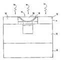
- FIG. 3shows the device of FIG. 2 in a third phase of the method, at the annealing step. Note that the device 1 has been rotated over 180° with respect to FIG. 2 .
- 15denotes a second insulating layer and 16 is a second carrier layer. 17 is a second surface of the semiconductor layer 4 .
- the second gate regioncomprises a second gate insulating layer 18 and a second gate electrode 19 .
- the arrows hvindicate laser light.
- the device 1 of FIG. 2is shown in a next phase of the method.
- a second insulating layer 15has been deposited on top of the complete device 1 , at the side of the first surface 5 .
- the second insulating layeris e.g. a thick layer of silicon dioxide.
- the complete devicei.e. the SOI
- the second carrier layermay be any type of material, but will preferably be a silicon wafer or glass.
- the first carrier layer and the first insulating layerare removed, again by any known method.
- the semiconductor layer 4 with the first gate structure 4 , the S/D 10 , 11 , the extensions 12 , 13 , and the second gate region 14is rotated 180° with respect to the view of FIG. 2 .
- the first surface 5is now completely buried, and the second surface 17 opposite the first surface 5 is now exposed. It is to be noticed that the second surface 17 is completely flat, i.e. it has no topography.
- a first methodis shown in FIG. 3 in the form of laser thermal anneal, indicated by the arrows hv.
- laser radiation with a wave length of 308 nm(XeCl excimer laser) is applied to the second surface 17 with a fluency of between 400 and 1000 mJ/cm2, depending on the depth of the junction, or generally the thickness of the semiconductor layer, and on the semiconductor material.
- any other kind of lasermay be used as well, e.g. with wavelengths such as 532, 801 or 1064 nm.
- the laser intensityhas to be selected accordingly, in order to allow for different absorption characteristics of the (amorphous) semiconductor material.
- the amorphous layersDue to the different laser absorption and different melting temperatures of the amorphous and the crystalline silicon material, the amorphous layers are melted and re-grown into crystalline layers.
- the dopantsare thereby incorporated into the crystal lattice, and activated to a very high degree.
- a great advantage of this so-called laser thermal annealis that it is substantially diffusionless. To be more precise, in this annealing method the dopants will not diffuse into surrounding layers. As a result, the junctions obtained are highly activated and extremely abrupt
- the abruptness of the profilemay be as high as less than 2 nm/decade, preferably even down to about 1 nm/decade. This abruptness has never been possible in a double gate FET device.
- the finishing of the second gate 14may be executed by etching away the highly doped second gate region 14 .
- a second gate insulating layer 18may be deposited, followed by filling with a second gate electrode material 19 .
- a planarization stepmay be used.
- Another way of preparing the second gate and subsequently finishing ituses the enhanced low-temperature oxidization of heavily doped silicon. The material thus obtained may be etched in a subsequent step, and filled with electrode material. This will however not be elucidated further.
- a step of solid phase epitaxy regrowth or SPERis performed.
- the amorphous materialstarts to recrystallize, whereby the dopants are built into the regrown crystal lattice.
- Temperaturesshould be selected to be sufficiently low to prevent diffusion of the dopants.
- Preferred temperatures for SPERdepend on the semiconductor material used, and for silicon these temperatures are between 500° C. and 800° C.
- the duration of the SPER stepdepends on the thickness of the amorphous layers, of the junction (extensions) and/or of the second gate 14 , and also on the selected temperature. The person skilled in the art will easily select the appropriate duration on the basis of layer thickness and selected temperature.
- laser thermal annealby using SPER it is possible to prevent diffusion of dopants into surrounding layers. Hence it is possible to obtain very abrupt and highly activated junctions, with an abruptness of down to 1 nm/decade.
- the device 1 as shown in FIG. 3is now ready for the final production steps, which may be selected as desired, for instance silicidization etc. This will however not be elucidated further.
Landscapes
- Engineering & Computer Science (AREA)
- Physics & Mathematics (AREA)
- Condensed Matter Physics & Semiconductors (AREA)
- General Physics & Mathematics (AREA)
- Manufacturing & Machinery (AREA)
- Computer Hardware Design (AREA)
- Microelectronics & Electronic Packaging (AREA)
- Power Engineering (AREA)
- Insulated Gate Type Field-Effect Transistor (AREA)
- Thin Film Transistor (AREA)
- Formation Of Insulating Films (AREA)
Abstract
Description
Claims (9)
Applications Claiming Priority (3)
| Application Number | Priority Date | Filing Date | Title |
|---|---|---|---|
| EP03103279.0 | 2003-09-03 | ||
| EP03103279 | 2003-09-03 | ||
| PCT/IB2004/051454WO2005022648A1 (en) | 2003-09-03 | 2004-08-12 | Method of fabricating a double gate field effect transistor device, and such a double gate field effect transistor device |
Publications (2)
| Publication Number | Publication Date |
|---|---|
| US20070166922A1 US20070166922A1 (en) | 2007-07-19 |
| US7521323B2true US7521323B2 (en) | 2009-04-21 |
Family
ID=34259244
Family Applications (1)
| Application Number | Title | Priority Date | Filing Date |
|---|---|---|---|
| US10/570,478Expired - LifetimeUS7521323B2 (en) | 2003-09-03 | 2004-08-12 | Method of fabricating a double gate field effect transistor device, and such a double gate field effect transistor device |
Country Status (6)
| Country | Link |
|---|---|
| US (1) | US7521323B2 (en) |
| EP (1) | EP1665386A1 (en) |
| JP (1) | JP2007504660A (en) |
| KR (1) | KR20060071412A (en) |
| TW (1) | TW200511575A (en) |
| WO (1) | WO2005022648A1 (en) |
Cited By (55)
| Publication number | Priority date | Publication date | Assignee | Title |
|---|---|---|---|---|
| US20060149252A1 (en)* | 2004-12-30 | 2006-07-06 | Markworth Aaron D | Bone anchorage screw with built-in hinged plate |
| US20080093668A1 (en)* | 2004-12-28 | 2008-04-24 | Koninklijke Philips Electronics N.V. | Method for the Manufacture of a Semiconductor Device and a Semiconductor Device Obtained Through It |
| US8377783B2 (en) | 2010-09-30 | 2013-02-19 | Suvolta, Inc. | Method for reducing punch-through in a transistor device |
| US8400219B2 (en) | 2011-03-24 | 2013-03-19 | Suvolta, Inc. | Analog circuits having improved transistors, and methods therefor |
| US8404551B2 (en) | 2010-12-03 | 2013-03-26 | Suvolta, Inc. | Source/drain extension control for advanced transistors |
| US8421162B2 (en) | 2009-09-30 | 2013-04-16 | Suvolta, Inc. | Advanced transistors with punch through suppression |
| US8461875B1 (en) | 2011-02-18 | 2013-06-11 | Suvolta, Inc. | Digital circuits having improved transistors, and methods therefor |
| US8525271B2 (en) | 2011-03-03 | 2013-09-03 | Suvolta, Inc. | Semiconductor structure with improved channel stack and method for fabrication thereof |
| US8530286B2 (en) | 2010-04-12 | 2013-09-10 | Suvolta, Inc. | Low power semiconductor transistor structure and method of fabrication thereof |
| US8569156B1 (en) | 2011-05-16 | 2013-10-29 | Suvolta, Inc. | Reducing or eliminating pre-amorphization in transistor manufacture |
| US8569128B2 (en) | 2010-06-21 | 2013-10-29 | Suvolta, Inc. | Semiconductor structure and method of fabrication thereof with mixed metal types |
| US8599623B1 (en) | 2011-12-23 | 2013-12-03 | Suvolta, Inc. | Circuits and methods for measuring circuit elements in an integrated circuit device |
| US8614128B1 (en) | 2011-08-23 | 2013-12-24 | Suvolta, Inc. | CMOS structures and processes based on selective thinning |
| US8629016B1 (en) | 2011-07-26 | 2014-01-14 | Suvolta, Inc. | Multiple transistor types formed in a common epitaxial layer by differential out-diffusion from a doped underlayer |
| US8637955B1 (en) | 2012-08-31 | 2014-01-28 | Suvolta, Inc. | Semiconductor structure with reduced junction leakage and method of fabrication thereof |
| US8645878B1 (en) | 2011-08-23 | 2014-02-04 | Suvolta, Inc. | Porting a circuit design from a first semiconductor process to a second semiconductor process |
| US8713511B1 (en) | 2011-09-16 | 2014-04-29 | Suvolta, Inc. | Tools and methods for yield-aware semiconductor manufacturing process target generation |
| US8735987B1 (en) | 2011-06-06 | 2014-05-27 | Suvolta, Inc. | CMOS gate stack structures and processes |
| US8748270B1 (en) | 2011-03-30 | 2014-06-10 | Suvolta, Inc. | Process for manufacturing an improved analog transistor |
| US8748986B1 (en) | 2011-08-05 | 2014-06-10 | Suvolta, Inc. | Electronic device with controlled threshold voltage |
| US8759872B2 (en) | 2010-06-22 | 2014-06-24 | Suvolta, Inc. | Transistor with threshold voltage set notch and method of fabrication thereof |
| US8796048B1 (en) | 2011-05-11 | 2014-08-05 | Suvolta, Inc. | Monitoring and measurement of thin film layers |
| US8811068B1 (en) | 2011-05-13 | 2014-08-19 | Suvolta, Inc. | Integrated circuit devices and methods |
| US8819603B1 (en) | 2011-12-15 | 2014-08-26 | Suvolta, Inc. | Memory circuits and methods of making and designing the same |
| US8816754B1 (en) | 2012-11-02 | 2014-08-26 | Suvolta, Inc. | Body bias circuits and methods |
| US8863064B1 (en) | 2012-03-23 | 2014-10-14 | Suvolta, Inc. | SRAM cell layout structure and devices therefrom |
| US8877619B1 (en) | 2012-01-23 | 2014-11-04 | Suvolta, Inc. | Process for manufacture of integrated circuits with different channel doping transistor architectures and devices therefrom |
| US8883600B1 (en) | 2011-12-22 | 2014-11-11 | Suvolta, Inc. | Transistor having reduced junction leakage and methods of forming thereof |
| US8895327B1 (en) | 2011-12-09 | 2014-11-25 | Suvolta, Inc. | Tipless transistors, short-tip transistors, and methods and circuits therefor |
| US8970289B1 (en) | 2012-01-23 | 2015-03-03 | Suvolta, Inc. | Circuits and devices for generating bi-directional body bias voltages, and methods therefor |
| US8976575B1 (en) | 2013-08-29 | 2015-03-10 | Suvolta, Inc. | SRAM performance monitor |
| US8988153B1 (en) | 2013-03-09 | 2015-03-24 | Suvolta, Inc. | Ring oscillator with NMOS or PMOS variation insensitivity |
| US8994415B1 (en) | 2013-03-01 | 2015-03-31 | Suvolta, Inc. | Multiple VDD clock buffer |
| US8995204B2 (en) | 2011-06-23 | 2015-03-31 | Suvolta, Inc. | Circuit devices and methods having adjustable transistor body bias |
| US8999861B1 (en) | 2011-05-11 | 2015-04-07 | Suvolta, Inc. | Semiconductor structure with substitutional boron and method for fabrication thereof |
| US9041126B2 (en) | 2012-09-21 | 2015-05-26 | Mie Fujitsu Semiconductor Limited | Deeply depleted MOS transistors having a screening layer and methods thereof |
| US9054219B1 (en) | 2011-08-05 | 2015-06-09 | Mie Fujitsu Semiconductor Limited | Semiconductor devices having fin structures and fabrication methods thereof |
| US9070477B1 (en) | 2012-12-12 | 2015-06-30 | Mie Fujitsu Semiconductor Limited | Bit interleaved low voltage static random access memory (SRAM) and related methods |
| US9093997B1 (en) | 2012-11-15 | 2015-07-28 | Mie Fujitsu Semiconductor Limited | Slew based process and bias monitors and related methods |
| US9093550B1 (en) | 2012-01-31 | 2015-07-28 | Mie Fujitsu Semiconductor Limited | Integrated circuits having a plurality of high-K metal gate FETs with various combinations of channel foundation structure and gate stack structure and methods of making same |
| US9112495B1 (en) | 2013-03-15 | 2015-08-18 | Mie Fujitsu Semiconductor Limited | Integrated circuit device body bias circuits and methods |
| US9112057B1 (en) | 2012-09-18 | 2015-08-18 | Mie Fujitsu Semiconductor Limited | Semiconductor devices with dopant migration suppression and method of fabrication thereof |
| US9112484B1 (en) | 2012-12-20 | 2015-08-18 | Mie Fujitsu Semiconductor Limited | Integrated circuit process and bias monitors and related methods |
| US9236466B1 (en) | 2011-10-07 | 2016-01-12 | Mie Fujitsu Semiconductor Limited | Analog circuits having improved insulated gate transistors, and methods therefor |
| US9268885B1 (en) | 2013-02-28 | 2016-02-23 | Mie Fujitsu Semiconductor Limited | Integrated circuit device methods and models with predicted device metric variations |
| US9299801B1 (en) | 2013-03-14 | 2016-03-29 | Mie Fujitsu Semiconductor Limited | Method for fabricating a transistor device with a tuned dopant profile |
| US9299698B2 (en) | 2012-06-27 | 2016-03-29 | Mie Fujitsu Semiconductor Limited | Semiconductor structure with multiple transistors having various threshold voltages |
| US9319013B2 (en) | 2014-08-19 | 2016-04-19 | Mie Fujitsu Semiconductor Limited | Operational amplifier input offset correction with transistor threshold voltage adjustment |
| US9406567B1 (en) | 2012-02-28 | 2016-08-02 | Mie Fujitsu Semiconductor Limited | Method for fabricating multiple transistor devices on a substrate with varying threshold voltages |
| US9431068B2 (en) | 2012-10-31 | 2016-08-30 | Mie Fujitsu Semiconductor Limited | Dynamic random access memory (DRAM) with low variation transistor peripheral circuits |
| US9449967B1 (en) | 2013-03-15 | 2016-09-20 | Fujitsu Semiconductor Limited | Transistor array structure |
| US9478571B1 (en) | 2013-05-24 | 2016-10-25 | Mie Fujitsu Semiconductor Limited | Buried channel deeply depleted channel transistor |
| US9710006B2 (en) | 2014-07-25 | 2017-07-18 | Mie Fujitsu Semiconductor Limited | Power up body bias circuits and methods |
| US10074568B2 (en) | 2009-09-30 | 2018-09-11 | Mie Fujitsu Semiconductor Limited | Electronic devices and systems, and methods for making and using same |
| CN109233810A (en)* | 2010-10-18 | 2019-01-18 | 华盛顿大学商业化中心 | Chromophoric polymers point |
Families Citing this family (8)
| Publication number | Priority date | Publication date | Assignee | Title |
|---|---|---|---|---|
| GB0411621D0 (en) | 2004-05-25 | 2004-06-30 | Koninkl Philips Electronics Nv | Dual gate semiconductor device |
| JP4923419B2 (en)* | 2005-03-15 | 2012-04-25 | 富士通セミコンダクター株式会社 | Manufacturing method of semiconductor device |
| ATE467908T1 (en) | 2006-08-04 | 2010-05-15 | Nxp Bv | METHOD FOR PRODUCING A DOUBLE GATE TRANSISTOR |
| US20090035911A1 (en)* | 2007-07-30 | 2009-02-05 | Willy Rachmady | Method for forming a semiconductor device having abrupt ultra shallow epi-tip regions |
| US8592264B2 (en) | 2011-12-21 | 2013-11-26 | International Business Machines Corporation | Source-drain extension formation in replacement metal gate transistor device |
| KR101639868B1 (en) | 2014-07-28 | 2016-07-15 | 성균관대학교산학협력단 | Albumin conjugated temperature and pH-sensitive multi-block copolymer, a method of preparation thereof and drug delivery system using the same |
| US9466729B1 (en)* | 2015-05-08 | 2016-10-11 | Qualcomm Incorporated | Etch stop region based fabrication of bonded semiconductor structures |
| KR102639769B1 (en)* | 2018-11-22 | 2024-02-26 | 삼성디스플레이 주식회사 | Display apparatus and method of manufacturing the same |
Citations (5)
| Publication number | Priority date | Publication date | Assignee | Title |
|---|---|---|---|---|
| US6346446B1 (en) | 1998-06-01 | 2002-02-12 | Massachusetts Institute Of Technology | Methods of forming features of integrated circuits using modified buried layers |
| US20020160574A1 (en) | 2001-04-27 | 2002-10-31 | Zahurak John K. | Method of forming a dual-gated semiconductor-on-insulator device |
| US6504173B2 (en) | 1998-06-19 | 2003-01-07 | International Business Machines Corporation | Dual gate FET and process |
| US20030040130A1 (en)* | 2001-08-09 | 2003-02-27 | Mayur Abhilash J. | Method for selection of parameters for implant anneal of patterned semiconductor substrates and specification of a laser system |
| US6812527B2 (en)* | 2002-09-05 | 2004-11-02 | International Business Machines Corporation | Method to control device threshold of SOI MOSFET's |
Family Cites Families (4)
| Publication number | Priority date | Publication date | Assignee | Title |
|---|---|---|---|---|
| US6031269A (en)* | 1997-04-18 | 2000-02-29 | Advanced Micro Devices, Inc. | Quadruple gate field effect transistor structure for use in integrated circuit devices |
| US6037640A (en)* | 1997-11-12 | 2000-03-14 | International Business Machines Corporation | Ultra-shallow semiconductor junction formation |
| JP2003526210A (en)* | 2000-02-29 | 2003-09-02 | コーニンクレッカ フィリップス エレクトロニクス エヌ ヴィ | Semiconductor device and manufacturing method thereof |
| US6346466B1 (en)* | 2000-03-30 | 2002-02-12 | Advanced Micro Devices, Inc. | Planarization of a polysilicon layer surface by chemical mechanical polish to improve lithography and silicide formation |
- 2004
- 2004-08-12EPEP04769806Apatent/EP1665386A1/ennot_activeWithdrawn
- 2004-08-12JPJP2006525219Apatent/JP2007504660A/ennot_activeWithdrawn
- 2004-08-12WOPCT/IB2004/051454patent/WO2005022648A1/enactiveApplication Filing
- 2004-08-12KRKR1020067004549Apatent/KR20060071412A/ennot_activeWithdrawn
- 2004-08-12USUS10/570,478patent/US7521323B2/ennot_activeExpired - Lifetime
- 2004-08-31TWTW093126279Apatent/TW200511575A/enunknown
Patent Citations (5)
| Publication number | Priority date | Publication date | Assignee | Title |
|---|---|---|---|---|
| US6346446B1 (en) | 1998-06-01 | 2002-02-12 | Massachusetts Institute Of Technology | Methods of forming features of integrated circuits using modified buried layers |
| US6504173B2 (en) | 1998-06-19 | 2003-01-07 | International Business Machines Corporation | Dual gate FET and process |
| US20020160574A1 (en) | 2001-04-27 | 2002-10-31 | Zahurak John K. | Method of forming a dual-gated semiconductor-on-insulator device |
| US20030040130A1 (en)* | 2001-08-09 | 2003-02-27 | Mayur Abhilash J. | Method for selection of parameters for implant anneal of patterned semiconductor substrates and specification of a laser system |
| US6812527B2 (en)* | 2002-09-05 | 2004-11-02 | International Business Machines Corporation | Method to control device threshold of SOI MOSFET's |
Non-Patent Citations (2)
| Title |
|---|
| Murto R et al: "Activation and Deactivation Studies of Laser Thermal . . ."; International Conference on Ion Implantation Technology Proceedings; Sep. 17, 2002; pp. 155-158. |
| Murto R et al: "An Investigation of Species Dependence in Germanium Pre-Amorphized and Laser Thermal Annealed Ultra-Shallow Abrupt Junctions"; International Conference on Ion Implantation Technology Proceedings; Sep. 17, 2000; pp. 182-185. |
Cited By (117)
| Publication number | Priority date | Publication date | Assignee | Title |
|---|---|---|---|---|
| US20080093668A1 (en)* | 2004-12-28 | 2008-04-24 | Koninklijke Philips Electronics N.V. | Method for the Manufacture of a Semiconductor Device and a Semiconductor Device Obtained Through It |
| US7838367B2 (en)* | 2004-12-28 | 2010-11-23 | Nxp B.V. | Method for the manufacture of a semiconductor device and a semiconductor device obtained through it |
| US20060149252A1 (en)* | 2004-12-30 | 2006-07-06 | Markworth Aaron D | Bone anchorage screw with built-in hinged plate |
| US10325986B2 (en) | 2009-09-30 | 2019-06-18 | Mie Fujitsu Semiconductor Limited | Advanced transistors with punch through suppression |
| US9263523B2 (en) | 2009-09-30 | 2016-02-16 | Mie Fujitsu Semiconductor Limited | Advanced transistors with punch through suppression |
| US11062950B2 (en) | 2009-09-30 | 2021-07-13 | United Semiconductor Japan Co., Ltd. | Electronic devices and systems, and methods for making and using the same |
| US9508800B2 (en) | 2009-09-30 | 2016-11-29 | Mie Fujitsu Semiconductor Limited | Advanced transistors with punch through suppression |
| US8421162B2 (en) | 2009-09-30 | 2013-04-16 | Suvolta, Inc. | Advanced transistors with punch through suppression |
| US10074568B2 (en) | 2009-09-30 | 2018-09-11 | Mie Fujitsu Semiconductor Limited | Electronic devices and systems, and methods for making and using same |
| US10217668B2 (en) | 2009-09-30 | 2019-02-26 | Mie Fujitsu Semiconductor Limited | Electronic devices and systems, and methods for making and using the same |
| US11887895B2 (en) | 2009-09-30 | 2024-01-30 | United Semiconductor Japan Co., Ltd. | Electronic devices and systems, and methods for making and using the same |
| US9865596B2 (en) | 2010-04-12 | 2018-01-09 | Mie Fujitsu Semiconductor Limited | Low power semiconductor transistor structure and method of fabrication thereof |
| US8530286B2 (en) | 2010-04-12 | 2013-09-10 | Suvolta, Inc. | Low power semiconductor transistor structure and method of fabrication thereof |
| US9496261B2 (en) | 2010-04-12 | 2016-11-15 | Mie Fujitsu Semiconductor Limited | Low power semiconductor transistor structure and method of fabrication thereof |
| US8569128B2 (en) | 2010-06-21 | 2013-10-29 | Suvolta, Inc. | Semiconductor structure and method of fabrication thereof with mixed metal types |
| US9224733B2 (en) | 2010-06-21 | 2015-12-29 | Mie Fujitsu Semiconductor Limited | Semiconductor structure and method of fabrication thereof with mixed metal types |
| US9922977B2 (en) | 2010-06-22 | 2018-03-20 | Mie Fujitsu Semiconductor Limited | Transistor with threshold voltage set notch and method of fabrication thereof |
| US9418987B2 (en) | 2010-06-22 | 2016-08-16 | Mie Fujitsu Semiconductor Limited | Transistor with threshold voltage set notch and method of fabrication thereof |
| US8759872B2 (en) | 2010-06-22 | 2014-06-24 | Suvolta, Inc. | Transistor with threshold voltage set notch and method of fabrication thereof |
| US8377783B2 (en) | 2010-09-30 | 2013-02-19 | Suvolta, Inc. | Method for reducing punch-through in a transistor device |
| CN109233810A (en)* | 2010-10-18 | 2019-01-18 | 华盛顿大学商业化中心 | Chromophoric polymers point |
| CN109233810B (en)* | 2010-10-18 | 2022-05-03 | 华盛顿大学商业化中心 | Chromophoric polymer dots |
| US8686511B2 (en) | 2010-12-03 | 2014-04-01 | Suvolta, Inc. | Source/drain extension control for advanced transistors |
| US8404551B2 (en) | 2010-12-03 | 2013-03-26 | Suvolta, Inc. | Source/drain extension control for advanced transistors |
| US9006843B2 (en) | 2010-12-03 | 2015-04-14 | Suvolta, Inc. | Source/drain extension control for advanced transistors |
| US8563384B2 (en) | 2010-12-03 | 2013-10-22 | Suvolta, Inc. | Source/drain extension control for advanced transistors |
| US9985631B2 (en) | 2011-02-18 | 2018-05-29 | Mie Fujitsu Semiconductor Limited | Digital circuits having improved transistors, and methods therefor |
| US9184750B1 (en) | 2011-02-18 | 2015-11-10 | Mie Fujitsu Semiconductor Limited | Digital circuits having improved transistors, and methods therefor |
| US9838012B2 (en) | 2011-02-18 | 2017-12-05 | Mie Fujitsu Semiconductor Limited | Digital circuits having improved transistors, and methods therefor |
| US8461875B1 (en) | 2011-02-18 | 2013-06-11 | Suvolta, Inc. | Digital circuits having improved transistors, and methods therefor |
| US10250257B2 (en) | 2011-02-18 | 2019-04-02 | Mie Fujitsu Semiconductor Limited | Digital circuits having improved transistors, and methods therefor |
| US9680470B2 (en) | 2011-02-18 | 2017-06-13 | Mie Fujitsu Semiconductor Limited | Digital circuits having improved transistors, and methods therefor |
| US8525271B2 (en) | 2011-03-03 | 2013-09-03 | Suvolta, Inc. | Semiconductor structure with improved channel stack and method for fabrication thereof |
| US9111785B2 (en) | 2011-03-03 | 2015-08-18 | Mie Fujitsu Semiconductor Limited | Semiconductor structure with improved channel stack and method for fabrication thereof |
| US8400219B2 (en) | 2011-03-24 | 2013-03-19 | Suvolta, Inc. | Analog circuits having improved transistors, and methods therefor |
| US8847684B2 (en) | 2011-03-24 | 2014-09-30 | Suvolta, Inc. | Analog circuits having improved transistors, and methods therefor |
| US9231541B2 (en) | 2011-03-24 | 2016-01-05 | Mie Fujitsu Semiconductor Limited | Analog circuits having improved transistors, and methods therefor |
| US9093469B2 (en) | 2011-03-30 | 2015-07-28 | Mie Fujitsu Semiconductor Limited | Analog transistor |
| US8748270B1 (en) | 2011-03-30 | 2014-06-10 | Suvolta, Inc. | Process for manufacturing an improved analog transistor |
| US8796048B1 (en) | 2011-05-11 | 2014-08-05 | Suvolta, Inc. | Monitoring and measurement of thin film layers |
| US8999861B1 (en) | 2011-05-11 | 2015-04-07 | Suvolta, Inc. | Semiconductor structure with substitutional boron and method for fabrication thereof |
| US8811068B1 (en) | 2011-05-13 | 2014-08-19 | Suvolta, Inc. | Integrated circuit devices and methods |
| US9362291B1 (en) | 2011-05-13 | 2016-06-07 | Mie Fujitsu Semiconductor Limited | Integrated circuit devices and methods |
| US9741428B2 (en) | 2011-05-13 | 2017-08-22 | Mie Fujitsu Semiconductor Limited | Integrated circuit devices and methods |
| US9966130B2 (en) | 2011-05-13 | 2018-05-08 | Mie Fujitsu Semiconductor Limited | Integrated circuit devices and methods |
| US8569156B1 (en) | 2011-05-16 | 2013-10-29 | Suvolta, Inc. | Reducing or eliminating pre-amorphization in transistor manufacture |
| US9793172B2 (en) | 2011-05-16 | 2017-10-17 | Mie Fujitsu Semiconductor Limited | Reducing or eliminating pre-amorphization in transistor manufacture |
| US8937005B2 (en) | 2011-05-16 | 2015-01-20 | Suvolta, Inc. | Reducing or eliminating pre-amorphization in transistor manufacture |
| US9514940B2 (en) | 2011-05-16 | 2016-12-06 | Mie Fujitsu Semiconductor Limited | Reducing or eliminating pre-amorphization in transistor manufacture |
| US8735987B1 (en) | 2011-06-06 | 2014-05-27 | Suvolta, Inc. | CMOS gate stack structures and processes |
| US9281248B1 (en) | 2011-06-06 | 2016-03-08 | Mie Fujitsu Semiconductor Limited | CMOS gate stack structures and processes |
| US9508728B2 (en) | 2011-06-06 | 2016-11-29 | Mie Fujitsu Semiconductor Limited | CMOS gate stack structures and processes |
| US8995204B2 (en) | 2011-06-23 | 2015-03-31 | Suvolta, Inc. | Circuit devices and methods having adjustable transistor body bias |
| US8653604B1 (en) | 2011-07-26 | 2014-02-18 | Suvolta, Inc. | Multiple transistor types formed in a common epitaxial layer by differential out-diffusion from a doped underlayer |
| US8916937B1 (en) | 2011-07-26 | 2014-12-23 | Suvolta, Inc. | Multiple transistor types formed in a common epitaxial layer by differential out-diffusion from a doped underlayer |
| US8629016B1 (en) | 2011-07-26 | 2014-01-14 | Suvolta, Inc. | Multiple transistor types formed in a common epitaxial layer by differential out-diffusion from a doped underlayer |
| US8748986B1 (en) | 2011-08-05 | 2014-06-10 | Suvolta, Inc. | Electronic device with controlled threshold voltage |
| US8963249B1 (en) | 2011-08-05 | 2015-02-24 | Suvolta, Inc. | Electronic device with controlled threshold voltage |
| US9054219B1 (en) | 2011-08-05 | 2015-06-09 | Mie Fujitsu Semiconductor Limited | Semiconductor devices having fin structures and fabrication methods thereof |
| US8645878B1 (en) | 2011-08-23 | 2014-02-04 | Suvolta, Inc. | Porting a circuit design from a first semiconductor process to a second semiconductor process |
| US8614128B1 (en) | 2011-08-23 | 2013-12-24 | Suvolta, Inc. | CMOS structures and processes based on selective thinning |
| US9391076B1 (en) | 2011-08-23 | 2016-07-12 | Mie Fujitsu Semiconductor Limited | CMOS structures and processes based on selective thinning |
| US9117746B1 (en) | 2011-08-23 | 2015-08-25 | Mie Fujitsu Semiconductor Limited | Porting a circuit design from a first semiconductor process to a second semiconductor process |
| US8806395B1 (en) | 2011-08-23 | 2014-08-12 | Suvolta, Inc. | Porting a circuit design from a first semiconductor process to a second semiconductor process |
| US8713511B1 (en) | 2011-09-16 | 2014-04-29 | Suvolta, Inc. | Tools and methods for yield-aware semiconductor manufacturing process target generation |
| US9236466B1 (en) | 2011-10-07 | 2016-01-12 | Mie Fujitsu Semiconductor Limited | Analog circuits having improved insulated gate transistors, and methods therefor |
| US8895327B1 (en) | 2011-12-09 | 2014-11-25 | Suvolta, Inc. | Tipless transistors, short-tip transistors, and methods and circuits therefor |
| US9953974B2 (en) | 2011-12-09 | 2018-04-24 | Mie Fujitsu Semiconductor Limited | Tipless transistors, short-tip transistors, and methods and circuits therefor |
| US9385121B1 (en) | 2011-12-09 | 2016-07-05 | Mie Fujitsu Semiconductor Limited | Tipless transistors, short-tip transistors, and methods and circuits therefor |
| US10573644B2 (en) | 2011-12-09 | 2020-02-25 | Mie Fujitsu Semiconductor Limited | Tipless transistors, short-tip transistors, and methods and circuits therefor |
| US9583484B2 (en) | 2011-12-09 | 2017-02-28 | Mie Fujitsu Semiconductor Limited | Tipless transistors, short-tip transistors, and methods and circuits therefor |
| US11145647B2 (en) | 2011-12-09 | 2021-10-12 | United Semiconductor Japan Co., Ltd. | Tipless transistors, short-tip transistors, and methods and circuits therefor |
| US8819603B1 (en) | 2011-12-15 | 2014-08-26 | Suvolta, Inc. | Memory circuits and methods of making and designing the same |
| US9196727B2 (en) | 2011-12-22 | 2015-11-24 | Mie Fujitsu Semiconductor Limited | High uniformity screen and epitaxial layers for CMOS devices |
| US8883600B1 (en) | 2011-12-22 | 2014-11-11 | Suvolta, Inc. | Transistor having reduced junction leakage and methods of forming thereof |
| US9368624B2 (en) | 2011-12-22 | 2016-06-14 | Mie Fujitsu Semiconductor Limited | Method for fabricating a transistor with reduced junction leakage current |
| US8599623B1 (en) | 2011-12-23 | 2013-12-03 | Suvolta, Inc. | Circuits and methods for measuring circuit elements in an integrated circuit device |
| US9297850B1 (en) | 2011-12-23 | 2016-03-29 | Mie Fujitsu Semiconductor Limited | Circuits and methods for measuring circuit elements in an integrated circuit device |
| US8970289B1 (en) | 2012-01-23 | 2015-03-03 | Suvolta, Inc. | Circuits and devices for generating bi-directional body bias voltages, and methods therefor |
| US8877619B1 (en) | 2012-01-23 | 2014-11-04 | Suvolta, Inc. | Process for manufacture of integrated circuits with different channel doping transistor architectures and devices therefrom |
| US9385047B2 (en) | 2012-01-31 | 2016-07-05 | Mie Fujitsu Semiconductor Limited | Integrated circuits having a plurality of high-K metal gate FETs with various combinations of channel foundation structure and gate stack structure and methods of making same |
| US9093550B1 (en) | 2012-01-31 | 2015-07-28 | Mie Fujitsu Semiconductor Limited | Integrated circuits having a plurality of high-K metal gate FETs with various combinations of channel foundation structure and gate stack structure and methods of making same |
| US9406567B1 (en) | 2012-02-28 | 2016-08-02 | Mie Fujitsu Semiconductor Limited | Method for fabricating multiple transistor devices on a substrate with varying threshold voltages |
| US9424385B1 (en) | 2012-03-23 | 2016-08-23 | Mie Fujitsu Semiconductor Limited | SRAM cell layout structure and devices therefrom |
| US8863064B1 (en) | 2012-03-23 | 2014-10-14 | Suvolta, Inc. | SRAM cell layout structure and devices therefrom |
| US10217838B2 (en) | 2012-06-27 | 2019-02-26 | Mie Fujitsu Semiconductor Limited | Semiconductor structure with multiple transistors having various threshold voltages |
| US9299698B2 (en) | 2012-06-27 | 2016-03-29 | Mie Fujitsu Semiconductor Limited | Semiconductor structure with multiple transistors having various threshold voltages |
| US10014387B2 (en) | 2012-06-27 | 2018-07-03 | Mie Fujitsu Semiconductor Limited | Semiconductor structure with multiple transistors having various threshold voltages |
| US9812550B2 (en) | 2012-06-27 | 2017-11-07 | Mie Fujitsu Semiconductor Limited | Semiconductor structure with multiple transistors having various threshold voltages |
| US8637955B1 (en) | 2012-08-31 | 2014-01-28 | Suvolta, Inc. | Semiconductor structure with reduced junction leakage and method of fabrication thereof |
| US9105711B2 (en) | 2012-08-31 | 2015-08-11 | Mie Fujitsu Semiconductor Limited | Semiconductor structure with reduced junction leakage and method of fabrication thereof |
| US9112057B1 (en) | 2012-09-18 | 2015-08-18 | Mie Fujitsu Semiconductor Limited | Semiconductor devices with dopant migration suppression and method of fabrication thereof |
| US9041126B2 (en) | 2012-09-21 | 2015-05-26 | Mie Fujitsu Semiconductor Limited | Deeply depleted MOS transistors having a screening layer and methods thereof |
| US9431068B2 (en) | 2012-10-31 | 2016-08-30 | Mie Fujitsu Semiconductor Limited | Dynamic random access memory (DRAM) with low variation transistor peripheral circuits |
| US8816754B1 (en) | 2012-11-02 | 2014-08-26 | Suvolta, Inc. | Body bias circuits and methods |
| US9154123B1 (en) | 2012-11-02 | 2015-10-06 | Mie Fujitsu Semiconductor Limited | Body bias circuits and methods |
| US9319034B2 (en) | 2012-11-15 | 2016-04-19 | Mie Fujitsu Semiconductor Limited | Slew based process and bias monitors and related methods |
| US9093997B1 (en) | 2012-11-15 | 2015-07-28 | Mie Fujitsu Semiconductor Limited | Slew based process and bias monitors and related methods |
| US9070477B1 (en) | 2012-12-12 | 2015-06-30 | Mie Fujitsu Semiconductor Limited | Bit interleaved low voltage static random access memory (SRAM) and related methods |
| US9112484B1 (en) | 2012-12-20 | 2015-08-18 | Mie Fujitsu Semiconductor Limited | Integrated circuit process and bias monitors and related methods |
| US9276561B2 (en) | 2012-12-20 | 2016-03-01 | Mie Fujitsu Semiconductor Limited | Integrated circuit process and bias monitors and related methods |
| US9268885B1 (en) | 2013-02-28 | 2016-02-23 | Mie Fujitsu Semiconductor Limited | Integrated circuit device methods and models with predicted device metric variations |
| US8994415B1 (en) | 2013-03-01 | 2015-03-31 | Suvolta, Inc. | Multiple VDD clock buffer |
| US8988153B1 (en) | 2013-03-09 | 2015-03-24 | Suvolta, Inc. | Ring oscillator with NMOS or PMOS variation insensitivity |
| US9299801B1 (en) | 2013-03-14 | 2016-03-29 | Mie Fujitsu Semiconductor Limited | Method for fabricating a transistor device with a tuned dopant profile |
| US9577041B2 (en) | 2013-03-14 | 2017-02-21 | Mie Fujitsu Semiconductor Limited | Method for fabricating a transistor device with a tuned dopant profile |
| US9893148B2 (en) | 2013-03-14 | 2018-02-13 | Mie Fujitsu Semiconductor Limited | Method for fabricating a transistor device with a tuned dopant profile |
| US9548086B2 (en) | 2013-03-15 | 2017-01-17 | Mie Fujitsu Semiconductor Limited | Integrated circuit device body bias circuits and methods |
| US9853019B2 (en) | 2013-03-15 | 2017-12-26 | Mie Fujitsu Semiconductor Limited | Integrated circuit device body bias circuits and methods |
| US9449967B1 (en) | 2013-03-15 | 2016-09-20 | Fujitsu Semiconductor Limited | Transistor array structure |
| US9112495B1 (en) | 2013-03-15 | 2015-08-18 | Mie Fujitsu Semiconductor Limited | Integrated circuit device body bias circuits and methods |
| US9991300B2 (en) | 2013-05-24 | 2018-06-05 | Mie Fujitsu Semiconductor Limited | Buried channel deeply depleted channel transistor |
| US9478571B1 (en) | 2013-05-24 | 2016-10-25 | Mie Fujitsu Semiconductor Limited | Buried channel deeply depleted channel transistor |
| US9786703B2 (en) | 2013-05-24 | 2017-10-10 | Mie Fujitsu Semiconductor Limited | Buried channel deeply depleted channel transistor |
| US8976575B1 (en) | 2013-08-29 | 2015-03-10 | Suvolta, Inc. | SRAM performance monitor |
| US9710006B2 (en) | 2014-07-25 | 2017-07-18 | Mie Fujitsu Semiconductor Limited | Power up body bias circuits and methods |
| US9319013B2 (en) | 2014-08-19 | 2016-04-19 | Mie Fujitsu Semiconductor Limited | Operational amplifier input offset correction with transistor threshold voltage adjustment |
Also Published As
| Publication number | Publication date |
|---|---|
| KR20060071412A (en) | 2006-06-26 |
| TW200511575A (en) | 2005-03-16 |
| EP1665386A1 (en) | 2006-06-07 |
| US20070166922A1 (en) | 2007-07-19 |
| JP2007504660A (en) | 2007-03-01 |
| WO2005022648A1 (en) | 2005-03-10 |
Similar Documents
| Publication | Publication Date | Title |
|---|---|---|
| US7521323B2 (en) | Method of fabricating a double gate field effect transistor device, and such a double gate field effect transistor device | |
| KR100879494B1 (en) | Method of doping a semiconductor gate | |
| US7247547B2 (en) | Method of fabricating a field effect transistor having improved junctions | |
| US6544854B1 (en) | Silicon germanium CMOS channel | |
| US6709935B1 (en) | Method of locally forming a silicon/geranium channel layer | |
| US6380044B1 (en) | High-speed semiconductor transistor and selective absorption process forming same | |
| US7312500B2 (en) | Manufacturing method of semiconductor device suppressing short-channel effect | |
| US7118980B2 (en) | Solid phase epitaxy recrystallization by laser annealing | |
| US20070267660A1 (en) | Method and apparatus for forming a semiconductor substrate with a layer structure of activated dopants | |
| US8772095B2 (en) | Method of manufacturing semiconductor device using stress memorization technique | |
| JP2007515066A (en) | Semiconductor substrate with reduced junction leakage using solid phase epitaxial regrowth and method for producing the same | |
| US6426278B1 (en) | Projection gas immersion laser dopant process (PGILD) fabrication of diffusion halos | |
| JPH0945919A (en) | Semiconductor-on-insulator transistor | |
| US6387784B1 (en) | Method to reduce polysilicon depletion in MOS transistors | |
| CN100405581C (en) | Method for forming non-amorphous ultra-thin semiconductor devices using sacrificial implant layers | |
| EP1524699B1 (en) | Method for forming CMOS semiconductor devices having a notched gate insulator and devices thus obtained | |
| US7091097B1 (en) | End-of-range defect minimization in semiconductor device | |
| JP2008503098A (en) | Semiconductor-on-insulator semiconductor device and manufacturing method | |
| US9087772B2 (en) | Device and method for forming sharp extension region with controllable junction depth and lateral overlap | |
| US20030160233A1 (en) | Method of forming a semiconductor device having an energy absorbing layer and structure thereof | |
| US7348229B2 (en) | Method of manufacturing a semiconductor device and semiconductor device obtained with such a method | |
| KR100906283B1 (en) | Method for forming non-amorphous, ultra-thin semiconductor devices using sacrificial implantation layer |
Legal Events
| Date | Code | Title | Description |
|---|---|---|---|
| AS | Assignment | Owner name:KONNINKLIJKE PHILIPS ELECTRONICS, N.V., NETHERLAND Free format text:ASSIGNMENT OF ASSIGNORS INTEREST;ASSIGNORS:SURDEANU, RADU;PONOMAREV, YOURI;REEL/FRAME:017645/0325 Effective date:20060126 | |
| AS | Assignment | Owner name:NXP B.V., NETHERLANDS Free format text:ASSIGNMENT OF ASSIGNORS INTEREST;ASSIGNOR:KONINKLIJKE PHILIPS ELECTRONICS N.V.;REEL/FRAME:019719/0843 Effective date:20070704 Owner name:NXP B.V.,NETHERLANDS Free format text:ASSIGNMENT OF ASSIGNORS INTEREST;ASSIGNOR:KONINKLIJKE PHILIPS ELECTRONICS N.V.;REEL/FRAME:019719/0843 Effective date:20070704 | |
| STCF | Information on status: patent grant | Free format text:PATENTED CASE | |
| FEPP | Fee payment procedure | Free format text:PAYOR NUMBER ASSIGNED (ORIGINAL EVENT CODE: ASPN); ENTITY STATUS OF PATENT OWNER: LARGE ENTITY Free format text:PAYER NUMBER DE-ASSIGNED (ORIGINAL EVENT CODE: RMPN); ENTITY STATUS OF PATENT OWNER: LARGE ENTITY | |
| AS | Assignment | Owner name:IMEC, BELGIUM Free format text:ASSIGNMENT OF ASSIGNORS INTEREST;ASSIGNOR:NXP B.V.;REEL/FRAME:027654/0244 Effective date:20120125 | |
| FPAY | Fee payment | Year of fee payment:4 | |
| FPAY | Fee payment | Year of fee payment:8 | |
| MAFP | Maintenance fee payment | Free format text:PAYMENT OF MAINTENANCE FEE, 12TH YEAR, LARGE ENTITY (ORIGINAL EVENT CODE: M1553); ENTITY STATUS OF PATENT OWNER: LARGE ENTITY Year of fee payment:12 |