US7521322B2 - Vertical transistors - Google Patents
Vertical transistorsDownload PDFInfo
- Publication number
- US7521322B2 US7521322B2US11/491,066US49106606AUS7521322B2US 7521322 B2US7521322 B2US 7521322B2US 49106606 AUS49106606 AUS 49106606AUS 7521322 B2US7521322 B2US 7521322B2
- Authority
- US
- United States
- Prior art keywords
- forming
- transistor
- mask
- ridge
- bit line
- Prior art date
- Legal status (The legal status is an assumption and is not a legal conclusion. Google has not performed a legal analysis and makes no representation as to the accuracy of the status listed.)
- Expired - Lifetime, expires
Links
Images


Classifications
- H—ELECTRICITY
- H10—SEMICONDUCTOR DEVICES; ELECTRIC SOLID-STATE DEVICES NOT OTHERWISE PROVIDED FOR
- H10B—ELECTRONIC MEMORY DEVICES
- H10B12/00—Dynamic random access memory [DRAM] devices
- H10B12/30—DRAM devices comprising one-transistor - one-capacitor [1T-1C] memory cells
- H10B12/48—Data lines or contacts therefor
- H10B12/482—Bit lines
- H—ELECTRICITY
- H01—ELECTRIC ELEMENTS
- H01L—SEMICONDUCTOR DEVICES NOT COVERED BY CLASS H10
- H01L21/00—Processes or apparatus adapted for the manufacture or treatment of semiconductor or solid state devices or of parts thereof
- H01L21/02—Manufacture or treatment of semiconductor devices or of parts thereof
- H01L21/04—Manufacture or treatment of semiconductor devices or of parts thereof the devices having potential barriers, e.g. a PN junction, depletion layer or carrier concentration layer
- H01L21/18—Manufacture or treatment of semiconductor devices or of parts thereof the devices having potential barriers, e.g. a PN junction, depletion layer or carrier concentration layer the devices having semiconductor bodies comprising elements of Group IV of the Periodic Table or AIIIBV compounds with or without impurities, e.g. doping materials
- H01L21/28—Manufacture of electrodes on semiconductor bodies using processes or apparatus not provided for in groups H01L21/20 - H01L21/268
- H01L21/28008—Making conductor-insulator-semiconductor electrodes
- H01L21/28017—Making conductor-insulator-semiconductor electrodes the insulator being formed after the semiconductor body, the semiconductor being silicon
- H01L21/28026—Making conductor-insulator-semiconductor electrodes the insulator being formed after the semiconductor body, the semiconductor being silicon characterised by the conductor
- H01L21/28123—Lithography-related aspects, e.g. sub-lithography lengths; Isolation-related aspects, e.g. to solve problems arising at the crossing with the side of the device isolation; Planarisation aspects
- H01L21/28132—Lithography-related aspects, e.g. sub-lithography lengths; Isolation-related aspects, e.g. to solve problems arising at the crossing with the side of the device isolation; Planarisation aspects conducting part of electrode is difined by a sidewall spacer or a similar technique, e.g. oxidation under mask, plating
- H—ELECTRICITY
- H10—SEMICONDUCTOR DEVICES; ELECTRIC SOLID-STATE DEVICES NOT OTHERWISE PROVIDED FOR
- H10B—ELECTRONIC MEMORY DEVICES
- H10B12/00—Dynamic random access memory [DRAM] devices
- H10B12/01—Manufacture or treatment
- H10B12/02—Manufacture or treatment for one transistor one-capacitor [1T-1C] memory cells
- H10B12/05—Making the transistor
- H10B12/053—Making the transistor the transistor being at least partially in a trench in the substrate
- H—ELECTRICITY
- H10—SEMICONDUCTOR DEVICES; ELECTRIC SOLID-STATE DEVICES NOT OTHERWISE PROVIDED FOR
- H10B—ELECTRONIC MEMORY DEVICES
- H10B12/00—Dynamic random access memory [DRAM] devices
- H10B12/30—DRAM devices comprising one-transistor - one-capacitor [1T-1C] memory cells
- H10B12/48—Data lines or contacts therefor
- H10B12/485—Bit line contacts
- H—ELECTRICITY
- H10—SEMICONDUCTOR DEVICES; ELECTRIC SOLID-STATE DEVICES NOT OTHERWISE PROVIDED FOR
- H10D—INORGANIC ELECTRIC SEMICONDUCTOR DEVICES
- H10D30/00—Field-effect transistors [FET]
- H10D30/01—Manufacture or treatment
- H10D30/021—Manufacture or treatment of FETs having insulated gates [IGFET]
- H10D30/025—Manufacture or treatment of FETs having insulated gates [IGFET] of vertical IGFETs
- H—ELECTRICITY
- H10—SEMICONDUCTOR DEVICES; ELECTRIC SOLID-STATE DEVICES NOT OTHERWISE PROVIDED FOR
- H10B—ELECTRONIC MEMORY DEVICES
- H10B12/00—Dynamic random access memory [DRAM] devices
- H10B12/30—DRAM devices comprising one-transistor - one-capacitor [1T-1C] memory cells
- H10B12/31—DRAM devices comprising one-transistor - one-capacitor [1T-1C] memory cells having a storage electrode stacked over the transistor
- H10B12/315—DRAM devices comprising one-transistor - one-capacitor [1T-1C] memory cells having a storage electrode stacked over the transistor with the capacitor higher than a bit line
Definitions
- the present inventionrelates to the field of integrated circuit fabrication, specifically to the formation of transistors.
- DRAMDynamic Random Access Memory
- RAMsemiconductor Random Access Memory
- DRAM memory cellscan shrink in several ways.
- One way to decrease the size of a memory cellis to reduce the minimum feature size (F). This generally occurs through new and advanced lithography and etching techniques.
- Memory cellscan also be decreased by designing a smaller memory cell. For example, many of the DRAM chips on the market today have a memory cell size of 8F 2 or greater, where F is the dimension of the minimum feature for a given manufacturing process.
- Vertical transistor designscan be used to decrease chip real estate occupied by a memory cell transistor.
- An example of a memory cell with a vertical transistoris disclosed in U.S. Pat. No. 6,756,625, issued to Brown, the disclosure of which is incorporate by reference herein.
- the digit lineis directly connected to a pillar used in the vertical transistor.
- thiscan be difficult to integrate into the process flow of a DRAM memory cell. Therefore, additional methods of forming vertical transistors are desirable.
- a memory arraycomprising a substrate having a plurality of ridges and trenches.
- a digit lineis within each of the plurality of trenches.
- a plurality of transistor pillarsoverlies each of the plurality of ridges.
- the transistor pillarsinclude an upper active area.
- a plurality of lower active areasis in an upper surface of each of the plurality of ridges.
- One of the lower active areasneighbors each transistor pillar.
- a digit line linkis within each trench connecting each lower active area to one digit line.
- the arrayalso includes a plurality of word lines, wherein each word line surrounds a row of transistor pillars over at least two of the plurality of ridges.
- a method of forming an integrated circuit including a vertical transistorcomprises defining a ridge region and a trench in a substrate.
- a digit lineis formed within the trench.
- An insulating materialis deposited in the trench to isolate the digit line.
- a transistor pillaris formed in the ridge region after depositing the insulating material in the trench.
- a portion of the digit line adjacent to the ridge regionis exposed after forming the transistor pillar.
- a digit line stitchis created within the trench connecting the digit line to a lower active area within the ridge region after exposing the portion of the digit line.
- a gate surrounding the transistor pillaris formed after depositing the digit line stitch.
- a method of forming a memory arraycomprises forming a digit line within each of a plurality of trenches in a substrate.
- a plurality of transistor pillarsis produced on each of a plurality of ridges in the substrate after forming the digit lines.
- Forming the pillarscomprises forming a column of transistor pillars on each ridge and rows of transistor pillars across different ridges.
- a word lineis formed to connect each row of transistor pillars.
- a plurality of exposed digit line windowsis created in the trench after forming the word lines.
- the methodfurther comprises forming a digit line stitch in each exposed digit line window to connect the digit lines to a lower active area of one neighboring transistor.
- a method of forming a memory arraycomprises forming a plurality of trenches and a plurality of plateaus within a substrate.
- a digit lineis deposited in each trench and the digit line is isolated within each trench.
- An exposed side portion of the digit lineis formed and a digit line strap is deposited to connect the exposed side portion of the digit line to a plurality of lower active areas in the plateaus.
- the plateausare etched to form transistor pillars and ridges in the substrate.
- a word line material surrounding the transistor pillarsis deposited. Vertical self-alignment spacers are formed surrounding an upper portion of the transistor pillars and over the word line material.
- the methodfurther comprises etching the word line material to form a plurality of word lines connecting a row of transistor pillars.
- a method of forming vertical transistor pillars in a substratecomprises forming a plurality of buried digit lines within a plurality of trenches in a substrate.
- a first maskis deposited on the substrate.
- a plurality of holesis formed in the first mask.
- a second maskis deposited in the holes of the first mask.
- the first maskis removed after depositing the second mask.
- the methodfurther comprises etching the substrate selectively to the second mask to form a plurality of pillars in the substrate above and adjacent to the buried digit lines.
- a vertical transistor for an integrated circuitcomprises a buried digit line within a trench in a bulk semiconductor substrate.
- a bulk semiconductor transistor pillaris on a ridge in the semiconductor substrate.
- a digit line linkis in the trench connecting the buried digit line to a lower active area in the ridge.
- the transistorfurther comprises a conductive gate surrounding the transistor pillar.
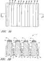
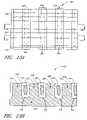
- FIG. 1Ais a schematic plan view of a memory array at a first stage of processing.
- FIG. 1Bis a schematic cross-section of the array of FIG. 1A along line 1 B- 1 B of FIG. 1A .
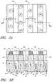
- FIG. 2Ais a schematic plan view of the memory array of FIG. 1A after removing part of the trench oxide and depositing a space holder.
- FIG. 2Bis a schematic cross-section of the array of FIG. 2A along line 2 B- 2 B of FIG. 2A .
- FIG. 3Ais a schematic plan view of the memory array of FIG. 2A after recessing the space holder.
- FIG. 3Bis a schematic cross-section of the array of FIG. 3A along line 3 B- 3 B of FIG. 3A .
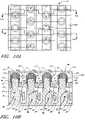
- FIG. 4Ais a schematic plan view of the memory array of FIG. 3A after deposition of a strap material.
- FIG. 4Bis a schematic cross-section of the array of FIG. 4A along line 4 B- 4 B of FIG. 4A .
- FIG. 5Ais a schematic plan view of the memory array of FIG. 4A after removing a cap over substrate ridges and patterning a masking layer.
- FIG. 5Bis a schematic cross-section of the array of FIG. 5A along line 5 B- 5 B of FIG. 5A .
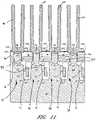
- FIG. 6Ais a schematic plan view of the memory array of FIG. 5A after an etch step.
- FIG. 6Bis a schematic cross-section of the array of FIG. 6A along line 6 B- 6 B of FIG. 6A .
- FIG. 7Ais a schematic plan view of the memory array of FIG. 6A after a spacer formation and an oxidation process.
- FIG. 7Bis a schematic cross-section of the array of FIG. 7A along line 7 B- 7 B of FIG. 7A .
- FIG. 8Ais a schematic plan view of the memory array of FIG. 7A after stripping spacers, forming a gate dielectric, and depositing a word line material.
- FIG. 8Bis a schematic cross-section of the array of FIG. 8A along line 8 B- 8 B of FIG. 8A .
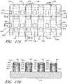
- FIG. 9Ais a schematic plan view of the memory array of FIG. 8A after forming self-alignment spacers and patterning word lines.
- FIG. 9Cis a schematic cross-section of the array of FIG. 9A along line 9 C- 9 C of FIG. 9A
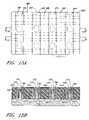
- FIG. 10Ais a schematic plan view of the memory array of FIG. 9A after depositing and planarizing an insulation layer.
- FIG. 10Bis a schematic cross-section of the array of FIG. 10A along line 10 B- 10 B of FIG. 10A .
- FIG. 10Cis a schematic cross-section of the array of FIG. 10A along line 10 C- 10 C of FIG. 10A
- FIG. 11is a schematic cross-section of the array of FIG. 10A after forming a lower capacitor electrode over each transistor.
- FIG. 12Ais a schematic plan view of a partially fabricated memory array in another preferred embodiment, showing a pattern of buried digit lines in parallel trenches.
- FIG. 12Bis a schematic cross-section of the array of FIG. 12A along line 12 B- 12 B of FIG. 12A .
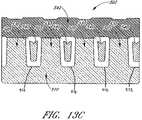
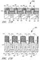
- FIGS. 13A-13Cschematically illustrate the memory array of FIG. 12A after depositing and patterning a first mask of lines crossing the digit line trenches.
- FIGS. 14A-14Cschematically illustrate the memory array of FIG. 13A rotated 90 degrees after forming a second mask to form exposed substrate windows, depositing a spacer in the exposed substrate windows and forming pillars epitaxially.
- FIGS. 15A-15Cschematically illustrate the memory array of FIG. 14A after forming word lines, an insulating layer, and a sacrificial mask.
- FIGS. 16A-16Cschematically illustrate the memory array of FIG. 15A after re-patterning the first mask and etching to expose lower active areas.
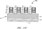
- FIGS. 17A-17Eschematically illustrate the memory array of FIG. 16A after exposing the digit line and depositing a spacer mask around the word lines.
- FIGS. 18A-18Eschematically illustrate the memory array of FIG. 17A -17E after forming stitches connecting the digit line with a lower active area.
- FIGS. 19A-19Cschematically illustrate the memory array of FIG. 18A after the removal of insulating materials over the pillars.
- semiconductor substrateis defined to mean any construction comprising semiconductor materials, including, but not limited to, bulk semiconductor materials such as a semiconductor wafers, and semiconductor material layers.
- substraterefers to any supporting substrate, including, but not limited to, the semiconductor substrates (either alone or in assemblies comprising other materials thereon) described above.
- layerencompasses both the singular and the plural unless otherwise indicated.
- VSGTsvertical surround gate transistors
- the memory cellshave a cell size of 4F 2 .
- transistorsare formed without using a separate interconnect outside of the isolation trench to connect a buried digit line and a lower active area.
- a digit line link within the isolation trenchis used to connect the digit line to the lower active area.
- a strap running the length of the arrayconnects the digit line to the lower active area of several transistors in a row.
- a conductive stitchis used to separately connect the digit line to the lower active area of one transistor. Additionally by using a buried digit line in the STI trench and strapping the buried digit line to the active area, less chip real estate is used than using other digit line placements.
- VSGTscan be formed using epitaxially grown silicon to form the pillar surrounded by the vertical surround gate (VSG).
- VSGvertical surround gate
- epitaxially grown siliconoften has high defect rates. It is challenging to overcome these defects or to form a defect free epitaxially grown silicon pillar, and also to integrate the process flow with digit line formation and contact.
- epitaxially grown siliconis not used, rather etch steps are used to define the transistor pillar. This eliminates the challenges of dealing with epitaxially-grown silicon.
- buried digit lines (BDL) 40are placed in shallow trench isolation (STI) trenches 12 within an array 2 .
- the buried digit lines 40are preferably connected to a lower active area 65 , which is formed in an upper surface of the substrate 10 , by a strap 60 within the trench 12 .
- the word line 95is preferably positioned above the buried digit line 40 .
- FIG. 1Aa schematic planar view of a portion of an array 2 can be seen.
- Trenches 12are seen lined with an insulation material 30 , between a pair of cap lines 25 over the substrate 10 .
- the trenchesare filled with an insulation material 45 ( FIG. 1B ) after depositing a digit line 40 ( FIG. 1B ) in each trench 12 .
- FIG. 1Ashows only the lining insulation material 30 within the trenches 12 .
- the trench liner 30 and the trench filler 45are similar materials.
- a p-wellhas been formed in the substrate 10 by doping the substrate 10 prior to forming the insulation trenches 12 .
- FIG. 1Bis a cross sectional schematic view of the array 2 of FIG. 1A .
- the substrate 10has been masked and etched to form trenches 12 between substrate plateaus within the substrate 10 .
- a pad oxide 20was formed on the surface of the substrate 10 .
- the pad oxide 20can be deposited by conventional depositional processes, such as chemical vapor deposition (CVD), or can be thermally grown on the surface of the substrate 10 .
- the pad oxide 20is between about 10 ⁇ and 100 ⁇ , more preferably between about 60 ⁇ and 100 ⁇ .
- Cap lines 25are deposited over the pad oxide 20 .
- the cap lines 25are a CVD grown silicon nitride layer with a thickness of between about 200 ⁇ and 800 ⁇ , more preferably between about 400 ⁇ and 600 ⁇ .
- the trenches 12are masked and etched.
- Various masking techniquescan be used to form the trenches 12 , including traditional photolithography and hard masks.
- the trench depthwill include an allowance for the height of a silicon pillar that will be used to form a vertical transistor, as well as a buried bit line within the trenches 12 .
- the trench depthwill be between about 5500 ⁇ and 8000 ⁇ , more preferably between about 6000 ⁇ and 7500 ⁇ .
- an insulation liner 30is formed over the surface of the array 2 .
- the lower layer of insulation material 30preferably oxide, is a TEOS (tetraethyl orthosilicate) oxide.
- the initial layer of trench oxide 30is formed over the entire array 2 and has a thickness of between about 50 ⁇ and 300 ⁇ , more preferably between about 100 ⁇ and 200 ⁇ and lines the trenches 12 without filling.
- a conductive line that will form the buried digit 40is formed within each trench 12 .
- the buried digit line 40is a conductor, more preferably a metal or a metal alloy, such as tungsten silicide (WSi x ).
- the metalis deposited conformally over the liner 30 by a CVD process or an atomic layer deposition (ALD) process.
- ALD processesallow for the formation of highly conformal layers.
- a blanket etchis performed to recess the metal that will become the buried digit line 40 , preferably etching down to between about 3000 ⁇ and 4000 ⁇ below the pad oxide 20 .
- a second layer of trench insulator 45is used to fill the remainder of the trench 12 .
- the second layer of trench insulator 45is formed similarly to the liner 30 and supplements the insulating capabilities of the liner 30 .
- the insulator 45is an oxide, more preferably a CVD TEOS oxide or a spin-on oxide.
- a chemical mechanical polish (CMP) step or other planarizing stepis performed to planarize the surface of the array 2 by removing excess materials over the height of the caps 25 .
- the CMP steppreferably is a stop-on-nitride process and stops on the cap layer 25 .
- the insulator 45is between about 3250 ⁇ to 4500 ⁇ thick over the digit line 40 . While the insulator 45 is shown in FIG. 1B , the first and second layers of insulator 30 , 45 are also referred to as one trench insulator 30 for convenience, and labeled as such in FIG. 1A and other figures.
- a maskis formed over the array 2 .
- a resist maskis formed to remove one side of the trench oxide 30 .
- the opening of a slot along one side and within the trench oxide 30will help in the formation of a strap that will eventually connect the buried digit line 40 to a lower active area.
- the etch processis selective to oxide and selective against silicon, nitrides, and metals.
- the resist maskmay also cover a portion of the cap layer 25 , but as the cap layer 25 is preferably not etched when removing a portion of the trench oxide 30 , whether the cap layer 25 is masked is not particularly important.
- the trench oxide 30can be etched all the way to the base of the trench 12 or the etch process can stop before the base of the trench 12 .
- a substantial portion of the buried digit line 40has been exposed by etching the trench oxide 30 .
- the oxide 30is etched on one side to a height of between about 0 ⁇ and 2000 ⁇ from the base of the trench 12 . In the embodiment illustrated in FIG. 2B , the trench oxide 30 is etched to a point about halfway along the height of the buried digit line 40 .
- FIGS. 2A and 2Billustrate the deposition of a space holder 55 to fill the narrow trenches 12 that were exposed when the trench oxide 30 was etched.
- the space holder 55is a thin non-photo sensitive resist or organic layer, such as a conventional bottom anti-reflective coating (BARC) layer. BARC is used because it is easily removable selective to neighboring layers, but other materials could also be used.
- the space holder 55is preferably blanket deposited over the array 2 .
- FIGS. 3A and 3Billustrate etching the space holder 55 and recessing the trench oxide 30 .
- the space holder 55is etched first in order to expose the STI oxide, but some of the space holder 55 is retained to protect the buried digit line 40 during the oxide etch.
- the depth of the trench oxide 30 recess processis determined with reference to the desired height of the silicon pillar that is to be formed in the substrate 10 .
- the trench oxide 30is preferably recessed to a height slightly higher than the desired pillar base level. For example, if the silicon pillar is approximately 2500 ⁇ tall, the trench oxide 30 is etched approximately 2000 ⁇ .
- the trench insulator 30is recessed down between about 1500 ⁇ and 3000 ⁇ from the level of the cap layer 25 , more preferably down by between about 1750 ⁇ and 2500 ⁇ .
- Recessing oxidecan be done by many etching processes, including wet and dry etch processes. Skilled practitioners will appreciate that many etch processes can be used to recess the trench oxide 30 .
- the space holder 55is preferably removed by a selective plasma etch or wet etch process after recessing the trench oxide 30 .
- a short wet cleanis also performed in order to remove any silicon oxide formed on the exposed bulk silicon 10 .
- FIGS. 4A and 4Billustrate the blanket deposition and etch back of a strap layer 60 that will form the strap that will connect the buried digit line 40 to the adjacent silicon regions 65 that will form the lower active areas.
- the strap layer 60is a polysilicon layer, more preferably a highly n-doped polysilicon layer. It is deposited over the trench oxide 30 and contacts the buried digit line 40 and a portion of the substrate 20 that will eventually form the lower active areas 65 . By strapping the buried digit line 40 in the STI area to the lower active area 65 , a separate interconnect for the buried digit line and the active area is not necessary. Fabrication time and costs are reduced by not having to fabricate the separate interconnect.
- circuitry in the periphery outside of the array 2can be defined after depositing the strap layer 60 .
- a protective materialsuch as a TEOS oxide, is preferably formed over the array 2 during, e.g., CMOS fabrication in the periphery.
- the cap layer 25is preferably removed after forming the strap layer 60 .
- the cap layer 25is removed in a selective wet etch process.
- Preferred etchantsinclude phosphoric acid and derivatives of phosphoric acid. Skilled artisans will appreciate that there are several methods to remove silicon nitride selectively from a substrate. Additionally, the pad oxide 20 can also be removed.
- a structural layer 70preferably an oxide layer, has been deposited over the array.
- the structural layer 70is a TEOS oxide with a thickness of between about 600 ⁇ and 1100 ⁇ , more preferably between about 650 ⁇ and 1000 ⁇ .
- a plurality of holesis formed within the structural layer 70 .
- the holesexpose portions of the substrate 10 that will eventually form the transistor pillars.
- the holesare filled with another mask material 75 and planarized back to the structural layer 70 .
- the holes patternis formed using standard lithography and etch techniques, such as an anisotropic etch step. In the illustrated embodiment, the holes are formed in a staggered fashion in order to increase the density of memory cells.
- a deep implantpreferably a p+ implant, can be performed after the holes in the structural layer 70 are etched to expose a pillar region of the substrate 10 and before filling with the mask material 75 .
- the implantpreferably reaches the base of the substrate, which is preferably a p-doped well. This reduces the floating body effect in the silicon pillars.
- the floating body effectoccurs when the active region is isolated from the substrate by a lower source/drain region and the adjacent space charge region. This causes the floating transistor body to charge up and subsequently the discharge of the cell capacitor.
- the depletion zonescan be limited to the edges of the active areas and should not meet.
- the holes in the structural layer 70are filled with a protective mask material 75 , which is preferably silicon nitride. Any excess protective material 75 is removed by a blanket nitride etch over the structural layer 70 .
- the structural layer 70is sacrificial, so selectivity of the blanket nitride etch is relatively unimportant.
- the structural layer 70is removed and the protective material 75 is used to mask the substrate 10 to form a plurality of pillars 77 .
- a substrate ridge 78is formed between the trenches 12 that extends from the bottom level of the trenches 12 to the bottom level of the pillars 77 .
- the ridges 78are preferably wider than the pillars 77 so the ridges have rounded shoulders 479 .
- an in situ selective oxide etchis used to remove the TEOS oxide of the structural layer 70 .
- the protective mask 75can then be used as a mask during a selective silicon etch to form vertical silicon pillars 77 by recessing the strap material 60 and etching exposed bulk silicon from the substrate 10 .
- the height of the pillars 77is preferably determined by the height of the gate and the elevation for the cell capacitor contact.
- the height of the pillars 77 from the upper surface or shoulder portions 479 of the ridge 78is between about 1000 ⁇ and 2000 ⁇ , more preferably between about 1400 ⁇ and 1800 ⁇ .
- the straps 60are even with the shoulders 479 of the ridges 78 .
- a nitride liner 79has been deposited over the array 2 .
- the nitride liner 79preferably has a thickness of between 40 ⁇ and 100 ⁇ , more preferably 50 ⁇ and 80 ⁇ .
- a punch-through etchis performed to remove the nitride liner 79 from the strap 60 , the trench oxide 30 , and the base of the pillars 77 .
- the top surface of the substrate ridges 78 and the strap 60are then thermally oxidized in order to isolate the strap 60 , the pillars 77 and the ridges 78 from a word line that will subsequently be deposited.
- Thermal oxidation of the exposed siliconforms an isolation layer 80 with a thickness of between about 300 ⁇ and 500 ⁇ , more preferably between about 350 ⁇ and 450 ⁇ .
- the n-dopants of the poly strap 60diffuse into the substrate 10 to form the lower active areas 65 .
- a selective nitride strip or etchis preferably preformed to expose the sides of the pillars 77 by removing the spacers 79 . Because the spacers 79 are thin, only a small portion of the nitride cap 75 may also be removed during the nitride strip.
- the nitride strip or another separate oxide etch processpreferably removes a portion of the insulation layer 80 . After this step, the insulation layer 80 preferably has a thickness of between about 175 ⁇ and 325 ⁇ , more preferably between about 200 ⁇ and 300 ⁇ .
- a gate dielectric 90is formed upon the pillars 77 after the nitride 79 is stripped.
- a thin thermally grown silicon oxide layercan serve as the gate dielectric 90 .
- the gate dielectric 90can also be deposited.
- a word line material 95is blanket deposited and etched back.
- the word line 95 materialpreferably polysilicon, is deposited over the entire array 2 and recessed to reduce the thickness.
- the thickness of the word line 95is between about 500 ⁇ and 2000 ⁇ , more preferably between about 1000 ⁇ and 1500 ⁇ .
- the remaining thickness of the polysilicon used for the word line 95will determine the length (or more accurately described, the height) of the vertical surround gate adjacent a channel region defined in the pillar 77 .
- spacers 100have been formed around the pillars 77 .
- a nitride layeris preferably blanket deposited over the whole array and then anisotropically etched, preferably by a dry plasma etch. The etch preferably stops on the poly of the word line 95 to form spacers 100 around the vertical sidewalls of the pillars 77 .
- word line material surrounding the entire pillar 77is masked and will not be removed once the word line material 95 is etched to form distinct word lines, as best seen from FIG. 9C . This will perform the function of self-aligning the word line 95 to the transistor pillars 77 , ensuring that the gate surrounds the transistor pillar 77 .
- a maskpreferably a soft resist mask, is formed over the word line material 95 .
- the word line 95is then etched according to the mask to form distinct word lines 95 within the array 2 .
- the etch processpreferably stops on oxide, so as to stop the etch process upon hitting the trench oxide 40 or the insulation layer 80 .
- the word lines 95connect neighboring memory cells in order to help form a memory array 2 .
- an insulator layer 105has been deposited over the array 2 .
- a CMP stepis then performed on the insulator 105 to planarize the surface over the array.
- a blanket layer of an etch stop layer 108such as silicon nitride, is deposited over the array 2 .
- the caps 75 over the pillars 77are removed in order to provide a contact for a bottom capacitor electrode 110 .
- the top of the transistor pillars 77can be doped to form an upper active area 103 that serves as the drain of the vertical transistor.
- FIG. 11further illustrates the formation of bottom electrodes 110 for cell capacitors over the upper active area 103 of the pillar 77 .
- a capacitor contact plugcan be used between the bottom electrode 110 and the upper active area 103 .
- the bottom electrode 110is a container electrode.
- Preferred materials for the bottom electrode 110include polysilicon, tungsten, and titanium nitride.
- a lower electrodeis formed within a structural layer that is later removed.
- One preferred method for forming a bottom electrodeis described in U.S. Pat. No. 6,756,627, issued to Wu, et al., which is incorporated by reference herein.
- a bottom container capacitor electrodeis formed over a transistor using a separate contact.
- many methods of making a container capacitorare available.
- a capacitor dielectric and an upper electrodeare formed over the bottom electrode to complete the formation of the cell capacitors.
- the upper electrodeis a common electrode to the array.
- Preferred upper electrode materialsinclude tungsten, titanium nitride, metals and metal alloys.
- the capacitor dielectriccan also be common to the array.
- Preferred materials for the capacitor dielectricinclude tantalum oxide, hafnium oxide, and other metal oxides. Other methods of forming a capacitor can also be used to form the cell capacitor.
- Buried digit lines 40are formed within isolation trenches 12 and buried or isolated by a trench insulator 30 .
- a strap 60 running along the digit line 40 and also within the isolation trench 12connects the digit line 40 to the lower active area 65 within the substrate ridge 78 .
- the strap 60is recessed within the isolation trench 12 and so does not risk shorting to the word line 95 .
- the lower active areas 65are preferably in a substrate ridge 78 in the substrate 10 below transistor pillars 77 .
- the insulation layer 80 over the strap 60isolates the strap 60 from the word line 95 , which surrounds a row of transistor pillars 77 .
- the transistor pillars 77are formed from material of the substrate 10 that has been masked to form the pillars 77 , thus leaving a superior crystalline quality relative to epitaxial silicon.
- an insulator 105 and an etch stop layer 108also overlie the word line 95 .
- a cell capacitoris formed with a bottom electrode 110 over and electrically connected to the transistor pillar 77 .
- the bottom electrodesare directly connected to the transistor pillars, but a conductive plug or other connection device could be used to electrically connect each bottom electrode to its respective transistor pillar 77 .
- the cellsare completed by forming capacitor dielectrics and upper electrodes over the bottom electrode 110 .
- control circuitrycan be formed in the periphery and the memory cells can be further isolated. It should also be appreciated that adjacent memory cells can share elements, such as a source/drain region.
- connection between the active area and the buried digit lineis isolated to a series of isolated stitches, instead of a strap running the length of the buried digit line.
- a buried digit lineis formed within a trench lined with an insulation layer.
- FIG. 12Ais a surface view of the array 502 .
- the buried digit line 540is shown in FIG. 12B within an insulating layer 530 between ridges 505 .
- Nitride capsare preferably used over the ridges 505 during the deposition of the buried digit line 540 , but have been removed prior to the stage of FIG. 12B .
- the nitride capsare removed by a wet nitride strip.
- the ridges 505are preferably capped during formation of the buried digit line 540 with a nitride layer, but the nitride layer is preferably removed after the remainder of trenches have been filled with an oxide.
- a first mask materialpreferably nitride, is deposited over the array 502 . This is best illustrated in FIG. 13C .
- the first mask layerhas a thickness of between about 2000 ⁇ and 3000 ⁇ , more preferably between about 2250 ⁇ and 2750 ⁇ .
- the first mask materialis patterned to form a series of mask lines 542 .
- the mask lines 542serve as a mask for subsequent processing.
- a liner 544preferably nitride, is formed to line the gaps between the mask lines 544 .
- FIG. 14Ahas been rotated 90 degrees from the position of FIG. 13A , and the views of FIGS. 14B and 14C are parallel to the bit lines 540 .
- the liner 544is preferably thin, having a thickness of between about 30 ⁇ and 80 ⁇ .
- a second mask material 550 that can be etched selectively to the first mask material 542is deposited between the first mask lines 542 .
- the second mask material 550forms lines an oxide, more preferably a spin-on oxide.
- the second mask material 550is over the region 505 that will include the active area in the final structure.
- a CMP stepcan be performed to planarize the surface after deposition of the second mask material 542 .
- the CMP steppreferably stops on the nitride liner 544 .
- the second mask layer 550is patterned and etched after the CMP step.
- a photoresist soft maskis formed over the second mask material 550 , and can be formed in a pattern of lines crossing perpendicular to the lines of first mask material 542 and second mask material 550 .
- the second mask material 550is then etched selectively against the first mask material 542 to the substrate 510 . This pattern forms windows or holes 552 to the substrate where the VSG channel will be formed.
- the etch processis a selective oxide etch that will not substantially etch the first mask layer 542 .
- a spacer material 555preferably TEOS oxide, is deposited within the holes 552 formed by the patterning of the second mask material 542 .
- the spacer materialpreferably has a thickness of between 250 and 600 ⁇ , more preferably between 300 ⁇ and 500 ⁇ .
- a spacer etchis performed on the array to remove excess spacer material and to clean the exposed active area for a subsequent selective epitaxial growth (SEG) step that will form the VSG channel 560 .
- SEGselective epitaxial growth
- the pillar 560is preferably formed by selective epitaxial growth (SEG) within the narrowed windows or holes over the ridges 505 .
- the epitaxial siliconis preferably grown to a desired height, but a silicon etch step can be performed to remove excess epitaxial silicon.
- the pillar 560has a height of between about 1000 ⁇ and 2000 ⁇ , more preferably between about 1400 ⁇ and 1800 ⁇ .
- a selective oxide etchhas been performed to remove the spacer material 555 and the second mask material 550 .
- the etchstops on the liner 544 or exposed bulk silicon from the substrate 510 .
- the pillars 560are then oxidized or a deposition conducted to form a gate dielectric 563 surrounding the epitaxially grown silicon pillar 560 .
- Word lines 565are deposited between the mask lines 542 and surrounding the pillars 560 and the gate dielectric 563 in the spaces formerly occupied by the second mask material.
- the word lines 565are a conductive material, more preferably polysilicon.
- the word lines 565are preferably recessed to a height of between about 800 ⁇ and 1200 ⁇ , more preferably between about 900 ⁇ and 1100 ⁇ .
- a soft oxidationis optionally performed to smooth the exposed word line material 565 .
- a liner 568preferably nitride, is deposited over the array 502 .
- the liner 568has a thickness of between about 50 ⁇ and 200 ⁇ , more preferably 80 ⁇ and 150 ⁇ .
- a third hard mask material 570is deposited over the surface of the array 502 .
- the third hard mask material 570is polysilicon.
- a stop-on-nitride CMP stepcan be performed to planarize the surface of the array 502 .
- a photoresist soft maskis formed, preferably perpendicular to the word lines 565 , is formed over the array.
- the soft maskcovers a portion of the pillar 560 .
- the exposed regions from the first mask material 542are removed, leaving unexposed portions of the first mask material 542 .
- the removal of this portion of the first mask material 542results in the exposure of portions of the ridges 505 in the bulk substrate below the level of the pillars 560 .
- the sacrificial hard mask layer 570is used to protect the word lines and underlying materials during the nitride etch.
- the nitride etchpreferably stops on the oxide 530 in the trench 512 , but an overetch which exposes the buried digit line 540 should not cause substantial deleterious effects.
- a spacer 575is deposited over the word lines 565 and the sacrificial hard mask 570 .
- the spacer 575is an insulator such as a silicon oxide or silicon nitride layer, more preferably silicon nitride.
- the spacer 575preferably has a thickness of between about 100 ⁇ and 300 ⁇ , more preferably between about 150 ⁇ and 250 ⁇ .
- the spacer 575is used to provide a larger masking profile for an oxide etch that exposes the buried digit line 540 (see FIG. 17C ).
- a spacer etchis performed to remove the spacer 575 from horizontal surfaces, such as the surface of the sacrificial hard mask 570 and the exposed portion of the oxide 530 which is over the buried digit line 540 . Only a portion of the width of the buried digit line 540 is exposed due to the use of the third mask material 570 and the spacers 575 as masks, as best seen from the view of FIG. 17E .
- the buried digit lines 540can be exposed in one step or two depending on the materials used for the spacer 575 and the etch chemistries selected.
- the nitride spacer etchremoves only nitride, stopping on the STI oxide 530 .
- Exposed STI oxide 530can then be removed by using either a dry plasma etch process or a wet etch process that etches oxides selective to the spacer 575 material and the buried digit line 540 material.
- etchantsare available that etch oxide, but will not substantially etch nitrides and metals.
- Preferred wet etchantsinclude diluted hydrofluoric acid.
- Preferred dry etchants to expose the buried digit lines 540include fluorocarbon gases, such as CH x F y gases. Skilled practitioners will appreciate that there are several methods to selectively etch oxide.
- a corner 577 ( FIG. 17E ) of the ridges 505is preferably exposed.
- a dopantcan be implanted or diffused to prepare the active areas 577 for their role in the transistor as the source/drain regions.
- an n+ implantis performed after removing the spacer 575 from the surface of the active area 577 .
- the doping processcan also be performed before the formation of the spacer or after the formation of a connection material between the active area 577 and the buried digit line 540 .
- FIG. 17Dshows the word lines 565 surrounding the silicon pillars 560 .
- the sacrificial hard mask layer 570 and the liner 568overlie the word lines 565 .
- FIG. 17Eshows the spacer 575 and the caps 543 and how they were used to expose only a portion of the buried digit line 540 and active areas 577 in the ridges 505 .
- a blanket conductive materialis deposited over the array 502 in order to form the buried digit line stitches 580 .
- the stitches 580are polysilicon, more preferably doped polysilicon.
- FIGS. 18A-18Eillustrate the array after the blanket deposition of conductive material and a subsequent recess of the conductive material to form the stitches 580 .
- a reactive ion etch (RIE) processis used to recess the conductive material to form conductive stitches 580 connecting the buried digit line 540 to the active area corners 577 in the ridges 505 .
- the RIE processdoes not substantially etch nitrides while it etches polysilicon.
- the RIE processpreferably confines the stitches to a small area by removing the conductive material over various mask materials 542 , 568 , and 575 , which are preferably nitride. These layers act as a mask for the deposition and formation of the stitches 580 .
- the stitches 580are recessed to a height of between about 0 ⁇ and 1000 ⁇ over the active areas 577 , more preferably between about 250 ⁇ and 750 ⁇ over the active areas 577 ( FIG. 18B ).
- the third hard mask material 570is preferably removed by the RIE etch process which recesses the stitches 580 .
- the recessed stitches 580can be seen in FIG. 18B between the spacers 575 .
- FIG. 18Eshows the stitches 580 connecting the buried digit line 540 to the active areas 577 .
- the insulator 590is then preferably deposited over the array 502 .
- the insulator 590is preferably an oxide, more preferably a TEOS oxide or a spin-on deposition (SOD) oxide.
- a stop-on-nitride CMP stepis then performed to planarize the surface of the array 502 .
- FIGS. 19A-19Cillustrate the removal of the insulating materials over the pillars 560 .
- Both the spacer 568 and the insulator 590 over the pillar 560are removed in this step.
- a photoresist maskis formed over the surface of the array 502 .
- a two step etch processcan be used to contact the pillar 560 .
- the insulator 590is recessed to the spacer 568 over the pillar 560 .
- a nitride punchcan then be performed to contact the top of the pillar 560 , which is preferably the drain site and will serve as the cell capacitor contact.
- Preferred nitride punch processesinclude an in situ punch etch or a separate nitride punch etch after the resist is removed.
- a capacitorcan be formed over the pillar 560 in order to form a memory cell.
- An etch stop linercan be deposited over the exposed insulator 590 .
- the cell capacitoris preferably a container electrode formed within a structural layer.
- Preferred materials for the bottom electrode 110include polysilicon, tungsten, and titanium nitride.
- one preferred method for forming a bottom electrodeis described in U.S. Pat. No. 6,756,627, issued to Wu, et al, which is previously incorporated by reference. Other methods of forming a capacitor are also available.
- FIGS. 19A-19CThe structure of the array of transistors can be seen in FIGS. 19A-19C .
- buried digit lines 540are within a trench in a substrate isolated by a trench oxide 530 .
- Transistor pillars 560are formed above substrate ridges 505 between the isolation trenches.
- Word lines 565overlie the substrate 510 , in which lower active areas 577 are formed.
- the buried digit lines 540are connected to individual transistor lower active areas 577 by individual connection stitches 580 .
- the stitches 580are polysilicon, more preferably n-doped polysilicon.
- the word lines 565surround the epitaxially-grown silicon pillars 560 (see FIG. 19B ).
- the tops of the pillars 560are preferably n-doped for use as an upper active area 592 .
- the upper active area 592serves as the drain of the transistor.
- the pillar 560is preferably epitaxially grown silicon, but it could also be etched from the substrate. Other materials can also be used in forming the vertical transistor.
- the transistoris used in a memory cell for a memory device such as a DRAM.
- a stacked capacitoris formed over the pillar 560 .
- the top of the pillarmay act as a cell capacitor contact, or a separate cell capacitor contact can be formed over the pillar 560 .
- a cell capacitoris formed over each pillar 560 .
- the cell capacitoris a container capacitor, which comprises a lower electrode electrically connected to the vertical transistor, preferably through the pillar 560 .
- a capacitor dielectric, such as a metal oxide,is formed over the container capacitor lower electrode.
- An upper electrodeis formed over the capacitor dielectric. In a preferred embodiment, the capacitor dielectric and the upper electrode are common to the entire array.
Landscapes
- Engineering & Computer Science (AREA)
- Manufacturing & Machinery (AREA)
- Physics & Mathematics (AREA)
- Condensed Matter Physics & Semiconductors (AREA)
- General Physics & Mathematics (AREA)
- Computer Hardware Design (AREA)
- Microelectronics & Electronic Packaging (AREA)
- Power Engineering (AREA)
- Semiconductor Memories (AREA)
Abstract
Description
Claims (23)
Priority Applications (1)
| Application Number | Priority Date | Filing Date | Title |
|---|---|---|---|
| US11/491,066US7521322B2 (en) | 2004-09-02 | 2006-07-21 | Vertical transistors |
Applications Claiming Priority (2)
| Application Number | Priority Date | Filing Date | Title |
|---|---|---|---|
| US10/934,621US7285812B2 (en) | 2004-09-02 | 2004-09-02 | Vertical transistors |
| US11/491,066US7521322B2 (en) | 2004-09-02 | 2006-07-21 | Vertical transistors |
Related Parent Applications (1)
| Application Number | Title | Priority Date | Filing Date |
|---|---|---|---|
| US10/934,621DivisionUS7285812B2 (en) | 2004-09-02 | 2004-09-02 | Vertical transistors |
Publications (2)
| Publication Number | Publication Date |
|---|---|
| US20060258084A1 US20060258084A1 (en) | 2006-11-16 |
| US7521322B2true US7521322B2 (en) | 2009-04-21 |
Family
ID=35941831
Family Applications (2)
| Application Number | Title | Priority Date | Filing Date |
|---|---|---|---|
| US10/934,621Expired - LifetimeUS7285812B2 (en) | 2004-09-02 | 2004-09-02 | Vertical transistors |
| US11/491,066Expired - LifetimeUS7521322B2 (en) | 2004-09-02 | 2006-07-21 | Vertical transistors |
Family Applications Before (1)
| Application Number | Title | Priority Date | Filing Date |
|---|---|---|---|
| US10/934,621Expired - LifetimeUS7285812B2 (en) | 2004-09-02 | 2004-09-02 | Vertical transistors |
Country Status (1)
| Country | Link |
|---|---|
| US (2) | US7285812B2 (en) |
Cited By (40)
| Publication number | Priority date | Publication date | Assignee | Title |
|---|---|---|---|---|
| US20090242975A1 (en)* | 2008-03-28 | 2009-10-01 | Samsung Electronics Co., Ltd. | Vertical pillar transistor |
| US20100219467A1 (en)* | 2009-03-02 | 2010-09-02 | Hynix Semiconductor Inc. | Semiconductor device having saddle fin transistor and manufacturing method of the same |
| US20100222832A1 (en)* | 2005-05-10 | 2010-09-02 | Yongxing Zhang | Methods for using a pulmonary artery electrode |
| US7858471B2 (en) | 2006-09-13 | 2010-12-28 | Micron Technology, Inc. | Methods of fabricating an access transistor for an integrated circuit device, methods of fabricating periphery transistors and access transistors, and methods of fabricating an access device comprising access transistors in an access circuitry region and peripheral transistors in a peripheral circuitry region spaced from the access circuitry region |
| US20110042722A1 (en)* | 2009-08-21 | 2011-02-24 | Nanya Technology Corp. | Integrated circuit structure and memory array |
| US7935999B2 (en) | 2005-09-01 | 2011-05-03 | Micron Technology, Inc. | Memory device |
| US7939409B2 (en) | 2005-09-01 | 2011-05-10 | Micron Technology, Inc. | Peripheral gate stacks and recessed array gates |
| US7977236B2 (en) | 2005-09-01 | 2011-07-12 | Micron Technology, Inc. | Method of forming a transistor gate of a recessed access device, method of forming a recessed transistor gate and a non-recessed transistor gate, and method of fabricating an integrated circuit |
| US20120001284A1 (en)* | 2010-06-30 | 2012-01-05 | President And Fellows Of Harvard College | Silicon nitride light pipes for image sensors |
| US20120119277A1 (en)* | 2010-11-12 | 2012-05-17 | Nanya Technology Corp. | Memory device and method of fabricating the same |
| US8222105B2 (en) | 2005-08-31 | 2012-07-17 | Micron Technology, Inc. | Methods of fabricating a memory device |
| US8274106B2 (en) | 2004-07-20 | 2012-09-25 | Micron Technology, Inc. | DRAM layout with vertical FETs and method of formation |
| US8471190B2 (en) | 2008-11-13 | 2013-06-25 | Zena Technologies, Inc. | Vertical waveguides with various functionality on integrated circuits |
| US8497541B2 (en) | 2010-03-10 | 2013-07-30 | Micron Technology, Inc. | Memory having buried digit lines and methods of making the same |
| US8507840B2 (en) | 2010-12-21 | 2013-08-13 | Zena Technologies, Inc. | Vertically structured passive pixel arrays and methods for fabricating the same |
| US8514411B2 (en) | 2009-05-26 | 2013-08-20 | Zena Technologies, Inc. | Determination of optimal diameters for nanowires |
| US8519379B2 (en) | 2009-12-08 | 2013-08-27 | Zena Technologies, Inc. | Nanowire structured photodiode with a surrounding epitaxially grown P or N layer |
| US8527064B2 (en) | 2007-12-12 | 2013-09-03 | Cardiac Pacemakers, Inc. | System for stimulating autonomic targets from pulmonary artery |
| US8546742B2 (en) | 2009-06-04 | 2013-10-01 | Zena Technologies, Inc. | Array of nanowires in a single cavity with anti-reflective coating on substrate |
| US8735797B2 (en) | 2009-12-08 | 2014-05-27 | Zena Technologies, Inc. | Nanowire photo-detector grown on a back-side illuminated image sensor |
| US8748799B2 (en) | 2010-12-14 | 2014-06-10 | Zena Technologies, Inc. | Full color single pixel including doublet or quadruplet si nanowires for image sensors |
| US8766272B2 (en) | 2009-12-08 | 2014-07-01 | Zena Technologies, Inc. | Active pixel sensor with nanowire structured photodetectors |
| US8791470B2 (en) | 2009-10-05 | 2014-07-29 | Zena Technologies, Inc. | Nano structured LEDs |
| US8835905B2 (en) | 2010-06-22 | 2014-09-16 | Zena Technologies, Inc. | Solar blind ultra violet (UV) detector and fabrication methods of the same |
| US8866065B2 (en) | 2010-12-13 | 2014-10-21 | Zena Technologies, Inc. | Nanowire arrays comprising fluorescent nanowires |
| US8889455B2 (en) | 2009-12-08 | 2014-11-18 | Zena Technologies, Inc. | Manufacturing nanowire photo-detector grown on a back-side illuminated image sensor |
| US9000353B2 (en) | 2010-06-22 | 2015-04-07 | President And Fellows Of Harvard College | Light absorption and filtering properties of vertically oriented semiconductor nano wires |
| US9082673B2 (en) | 2009-10-05 | 2015-07-14 | Zena Technologies, Inc. | Passivated upstanding nanostructures and methods of making the same |
| US9287271B2 (en) | 2011-08-23 | 2016-03-15 | Micron Technology, Inc. | Vertical transistor devices, memory arrays, and methods of forming vertical transistor devices |
| US9299866B2 (en) | 2010-12-30 | 2016-03-29 | Zena Technologies, Inc. | Nanowire array based solar energy harvesting device |
| US9343490B2 (en) | 2013-08-09 | 2016-05-17 | Zena Technologies, Inc. | Nanowire structured color filter arrays and fabrication method of the same |
| US9406709B2 (en) | 2010-06-22 | 2016-08-02 | President And Fellows Of Harvard College | Methods for fabricating and using nanowires |
| US9429723B2 (en) | 2008-09-04 | 2016-08-30 | Zena Technologies, Inc. | Optical waveguides in image sensors |
| US9478685B2 (en) | 2014-06-23 | 2016-10-25 | Zena Technologies, Inc. | Vertical pillar structured infrared detector and fabrication method for the same |
| US9515218B2 (en) | 2008-09-04 | 2016-12-06 | Zena Technologies, Inc. | Vertical pillar structured photovoltaic devices with mirrors and optical claddings |
| US20170162446A1 (en)* | 2015-12-07 | 2017-06-08 | International Business Machines Corporation | Multiple gate length vertical field-effect-transistors |
| TWI642064B (en)* | 2017-09-01 | 2018-11-21 | 美商格芯(美國)集成電路科技有限公司 | Bit line strapping scheme for high density sram |
| US10515801B2 (en) | 2007-06-04 | 2019-12-24 | Micron Technology, Inc. | Pitch multiplication using self-assembling materials |
| KR20200003722A (en)* | 2018-07-02 | 2020-01-10 | 타이완 세미콘덕터 매뉴팩쳐링 컴퍼니 리미티드 | Method of manufacturing a semiconductor device and a semiconductor device |
| US10943819B2 (en)* | 2018-12-20 | 2021-03-09 | Nanya Technology Corporation | Semiconductor structure having a plurality of capped protrusions |
Families Citing this family (95)
| Publication number | Priority date | Publication date | Assignee | Title |
|---|---|---|---|---|
| US5977579A (en)* | 1998-12-03 | 1999-11-02 | Micron Technology, Inc. | Trench dram cell with vertical device and buried word lines |
| US7071043B2 (en) | 2002-08-15 | 2006-07-04 | Micron Technology, Inc. | Methods of forming a field effect transistor having source/drain material over insulative material |
| US6844591B1 (en)* | 2003-09-17 | 2005-01-18 | Micron Technology, Inc. | Method of forming DRAM access transistors |
| US7262089B2 (en)* | 2004-03-11 | 2007-08-28 | Micron Technology, Inc. | Methods of forming semiconductor structures |
| US7547945B2 (en) | 2004-09-01 | 2009-06-16 | Micron Technology, Inc. | Transistor devices, transistor structures and semiconductor constructions |
| US7285812B2 (en)* | 2004-09-02 | 2007-10-23 | Micron Technology, Inc. | Vertical transistors |
| KR100618875B1 (en)* | 2004-11-08 | 2006-09-04 | 삼성전자주식회사 | Semiconductor memory device having vertical channel MOOS transistor and method of manufacturing same |
| US7199419B2 (en)* | 2004-12-13 | 2007-04-03 | Micron Technology, Inc. | Memory structure for reduced floating body effect |
| US7326611B2 (en)* | 2005-02-03 | 2008-02-05 | Micron Technology, Inc. | DRAM arrays, vertical transistor structures and methods of forming transistor structures and DRAM arrays |
| US7244659B2 (en)* | 2005-03-10 | 2007-07-17 | Micron Technology, Inc. | Integrated circuits and methods of forming a field effect transistor |
| US7384849B2 (en)* | 2005-03-25 | 2008-06-10 | Micron Technology, Inc. | Methods of forming recessed access devices associated with semiconductor constructions |
| US7120046B1 (en) | 2005-05-13 | 2006-10-10 | Micron Technology, Inc. | Memory array with surrounding gate access transistors and capacitors with global and staggered local bit lines |
| US7371627B1 (en) | 2005-05-13 | 2008-05-13 | Micron Technology, Inc. | Memory array with ultra-thin etched pillar surround gate access transistors and buried data/bit lines |
| US7888721B2 (en) | 2005-07-06 | 2011-02-15 | Micron Technology, Inc. | Surround gate access transistors with grown ultra-thin bodies |
| US7282401B2 (en) | 2005-07-08 | 2007-10-16 | Micron Technology, Inc. | Method and apparatus for a self-aligned recessed access device (RAD) transistor gate |
| US7768051B2 (en) | 2005-07-25 | 2010-08-03 | Micron Technology, Inc. | DRAM including a vertical surround gate transistor |
| US7776715B2 (en) | 2005-07-26 | 2010-08-17 | Micron Technology, Inc. | Reverse construction memory cell |
| US7867851B2 (en)* | 2005-08-30 | 2011-01-11 | Micron Technology, Inc. | Methods of forming field effect transistors on substrates |
| US7867845B2 (en)* | 2005-09-01 | 2011-01-11 | Micron Technology, Inc. | Transistor gate forming methods and transistor structures |
| KR100695514B1 (en)* | 2005-09-29 | 2007-03-16 | 주식회사 하이닉스반도체 | Metal wiring formation method of semiconductor device |
| KR100833182B1 (en)* | 2005-11-17 | 2008-05-28 | 삼성전자주식회사 | Semiconductor memory device having vertical channel transistor and method for fabricating the same device |
| US7700441B2 (en) | 2006-02-02 | 2010-04-20 | Micron Technology, Inc. | Methods of forming field effect transistors, methods of forming field effect transistor gates, methods of forming integrated circuitry comprising a transistor gate array and circuitry peripheral to the gate array, and methods of forming integrated circuitry comprising a transistor gate array including first gates and second grounded isolation gates |
| US20070262395A1 (en)* | 2006-05-11 | 2007-11-15 | Gibbons Jasper S | Memory cell access devices and methods of making the same |
| US8860174B2 (en)* | 2006-05-11 | 2014-10-14 | Micron Technology, Inc. | Recessed antifuse structures and methods of making the same |
| US8008144B2 (en) | 2006-05-11 | 2011-08-30 | Micron Technology, Inc. | Dual work function recessed access device and methods of forming |
| US7602001B2 (en) | 2006-07-17 | 2009-10-13 | Micron Technology, Inc. | Capacitorless one transistor DRAM cell, integrated circuitry comprising an array of capacitorless one transistor DRAM cells, and method of forming lines of capacitorless one transistor DRAM cells |
| US7772632B2 (en) | 2006-08-21 | 2010-08-10 | Micron Technology, Inc. | Memory arrays and methods of fabricating memory arrays |
| US7745319B2 (en)* | 2006-08-22 | 2010-06-29 | Micron Technology, Inc. | System and method for fabricating a fin field effect transistor |
| US7589995B2 (en) | 2006-09-07 | 2009-09-15 | Micron Technology, Inc. | One-transistor memory cell with bias gate |
| US8058683B2 (en)* | 2007-01-18 | 2011-11-15 | Samsung Electronics Co., Ltd. | Access device having vertical channel and related semiconductor device and a method of fabricating the access device |
| KR20100017559A (en)* | 2007-05-01 | 2010-02-16 | 웹텍 홀딩 코포레이션 | Compressible elastic spring |
| US7952138B2 (en)* | 2007-07-05 | 2011-05-31 | Qimonda Ag | Memory circuit with field effect transistor and method for manufacturing a memory circuit with field effect transistor |
| KR100950472B1 (en)* | 2007-12-28 | 2010-03-31 | 주식회사 하이닉스반도체 | Manufacturing Method of Semiconductor Device Having 4F2 Transistor |
| US20090176368A1 (en)* | 2008-01-08 | 2009-07-09 | Nan Wu | Manufacturing method for an integrated circuit structure comprising a selectively deposited oxide layer |
| KR100979240B1 (en)* | 2008-04-10 | 2010-08-31 | 주식회사 하이닉스반도체 | Semiconductor device and manufacturing method thereof |
| US7696056B2 (en)* | 2008-05-02 | 2010-04-13 | Micron Technology, Inc. | Methods of forming capacitors |
| US7618874B1 (en)* | 2008-05-02 | 2009-11-17 | Micron Technology, Inc. | Methods of forming capacitors |
| KR101010121B1 (en)* | 2008-07-04 | 2011-01-24 | 주식회사 하이닉스반도체 | Method of manufacturing semiconductor device |
| US7974119B2 (en) | 2008-07-10 | 2011-07-05 | Seagate Technology Llc | Transmission gate-based spin-transfer torque memory unit |
| KR101037495B1 (en) | 2008-07-31 | 2011-05-26 | 주식회사 하이닉스반도체 | Method of manufacturing highly integrated semiconductor device and semiconductor device |
| US7910971B2 (en) | 2008-08-07 | 2011-03-22 | Micron Technology, Inc. | Methods of forming vertical field effect transistors, vertical field effect transistors, and dram cells |
| US7979836B2 (en)* | 2008-08-15 | 2011-07-12 | International Business Machines Corporation | Split-gate DRAM with MuGFET, design structure, and method of manufacture |
| TWI368299B (en)* | 2008-08-15 | 2012-07-11 | Nanya Technology Corp | Vertical transistor and array of vertical transistor |
| US7781283B2 (en)* | 2008-08-15 | 2010-08-24 | International Business Machines Corporation | Split-gate DRAM with MuGFET, design structure, and method of manufacture |
| US20100090263A1 (en) | 2008-10-10 | 2010-04-15 | Qimonda Ag | Memory devices including semiconductor pillars |
| US8138538B2 (en)* | 2008-10-10 | 2012-03-20 | Qimonda Ag | Interconnect structure for semiconductor devices |
| KR101073073B1 (en)* | 2008-10-17 | 2011-10-12 | 주식회사 하이닉스반도체 | Semiconductor device with vertical gate and method for manufacturing the same |
| US9030867B2 (en) | 2008-10-20 | 2015-05-12 | Seagate Technology Llc | Bipolar CMOS select device for resistive sense memory |
| US7936580B2 (en) | 2008-10-20 | 2011-05-03 | Seagate Technology Llc | MRAM diode array and access method |
| US7936583B2 (en) | 2008-10-30 | 2011-05-03 | Seagate Technology Llc | Variable resistive memory punchthrough access method |
| US7824986B2 (en) | 2008-11-05 | 2010-11-02 | Micron Technology, Inc. | Methods of forming a plurality of transistor gates, and methods of forming a plurality of transistor gates having at least two different work functions |
| US7825478B2 (en) | 2008-11-07 | 2010-11-02 | Seagate Technology Llc | Polarity dependent switch for resistive sense memory |
| US8178864B2 (en) | 2008-11-18 | 2012-05-15 | Seagate Technology Llc | Asymmetric barrier diode |
| US8203869B2 (en) | 2008-12-02 | 2012-06-19 | Seagate Technology Llc | Bit line charge accumulation sensing for resistive changing memory |
| KR101528823B1 (en)* | 2009-01-19 | 2015-06-15 | 삼성전자주식회사 | Semiconductor memory device and method of manufacturing the same |
| KR20100099912A (en) | 2009-03-04 | 2010-09-15 | 삼성전자주식회사 | Semiconductor memory device and method of manufacturing the same |
| US8184472B2 (en)* | 2009-03-13 | 2012-05-22 | International Business Machines Corporation | Split-gate DRAM with lateral control-gate MuGFET |
| US7999332B2 (en)* | 2009-05-14 | 2011-08-16 | International Business Machines Corporation | Asymmetric semiconductor devices and method of fabricating |
| KR101077445B1 (en)* | 2009-05-28 | 2011-10-26 | 주식회사 하이닉스반도체 | Semiconductor having vertical channel transistor and manufacturing method of the same |
| US8159856B2 (en) | 2009-07-07 | 2012-04-17 | Seagate Technology Llc | Bipolar select device for resistive sense memory |
| US8158964B2 (en) | 2009-07-13 | 2012-04-17 | Seagate Technology Llc | Schottky diode switch and memory units containing the same |
| KR101576957B1 (en)* | 2009-10-22 | 2015-12-14 | 삼성전자주식회사 | Vertical semiconductor device, memory device, and manufacturing method thereof |
| CN102064098B (en)* | 2009-11-17 | 2012-10-24 | 台湾积体电路制造股份有限公司 | Growing III-V compound semiconductor from trench filled with intermediate layer |
| KR101096184B1 (en)* | 2009-11-30 | 2011-12-22 | 주식회사 하이닉스반도체 | Method for manufacturing side contact in semiconductor device using self aligned damascene process |
| US8148222B2 (en)* | 2009-12-10 | 2012-04-03 | Micron Technology, Inc. | Cross-point diode arrays and methods of manufacturing cross-point diode arrays |
| US8302688B2 (en) | 2010-01-20 | 2012-11-06 | Halliburton Energy Services, Inc. | Method of optimizing wellbore perforations using underbalance pulsations |
| US8716116B2 (en)* | 2010-03-10 | 2014-05-06 | Micron Technology, Inc. | Method of forming a DRAM array of devices with vertically integrated recessed access device and digitline |
| US8535992B2 (en)* | 2010-06-29 | 2013-09-17 | Micron Technology, Inc. | Thyristor random access memory device and method |
| US8617952B2 (en) | 2010-09-28 | 2013-12-31 | Seagate Technology Llc | Vertical transistor with hardening implatation |
| US8492845B2 (en) | 2010-11-05 | 2013-07-23 | International Business Machines Corporation | Gate-to-gate recessed strap and methods of manufacture of same |
| TWI415247B (en)* | 2010-12-15 | 2013-11-11 | Powerchip Technology Corp | Dynamic random access memory cell and array having vertical channel transistor |
| US8648426B2 (en) | 2010-12-17 | 2014-02-11 | Seagate Technology Llc | Tunneling transistors |
| KR101827549B1 (en) | 2011-01-03 | 2018-03-23 | 에스케이하이닉스 주식회사 | Semiconductor device and method for forming the same |
| US8697522B2 (en) | 2011-07-05 | 2014-04-15 | International Business Machines Corporation | Bulk finFET with uniform height and bottom isolation |
| US8691680B2 (en)* | 2011-07-14 | 2014-04-08 | Nanya Technology Corp. | Method for fabricating memory device with buried digit lines and buried word lines |
| US8672151B2 (en)* | 2011-09-15 | 2014-03-18 | Wabtec Corp | Elastomeric draft gear for a railcar |
| KR101906946B1 (en) | 2011-12-02 | 2018-10-12 | 삼성전자주식회사 | High density semiconductor memory device |
| US8437184B1 (en)* | 2011-12-06 | 2013-05-07 | Rexchip Electronics Corporation | Method of controlling a vertical dual-gate dynamic random access memory |
| JP2014022386A (en)* | 2012-07-12 | 2014-02-03 | Ps4 Luxco S A R L | Semiconductor device |
| US9064745B2 (en) | 2012-08-29 | 2015-06-23 | International Business Machines Corporation | Sublithographic width finFET employing solid phase epitaxy |
| US9589962B2 (en)* | 2014-06-17 | 2017-03-07 | Micron Technology, Inc. | Array of conductive vias, methods of forming a memory array, and methods of forming conductive vias |
| US10903210B2 (en)* | 2015-05-05 | 2021-01-26 | International Business Machines Corporation | Sub-fin doped bulk fin field effect transistor (FinFET), Integrated Circuit (IC) and method of manufacture |
| US9859284B2 (en)* | 2016-01-21 | 2018-01-02 | Micron Technology, Inc. | Semiconductor memory device having enlarged cell contact area and method of fabricating the same |
| US10854759B2 (en)* | 2016-04-01 | 2020-12-01 | Diodes Incorporated | Trenched MOS gate controlled rectifier |
| US9755073B1 (en)* | 2016-05-11 | 2017-09-05 | International Business Machines Corporation | Fabrication of vertical field effect transistor structure with strained channels |
| US9761580B1 (en) | 2016-11-01 | 2017-09-12 | Micron Technology, Inc. | Methods of forming an array comprising pairs of vertically opposed capacitors and arrays comprising pairs of vertically opposed capacitors |
| US10014305B2 (en) | 2016-11-01 | 2018-07-03 | Micron Technology, Inc. | Methods of forming an array comprising pairs of vertically opposed capacitors and arrays comprising pairs of vertically opposed capacitors |
| US10062745B2 (en) | 2017-01-09 | 2018-08-28 | Micron Technology, Inc. | Methods of forming an array of capacitors, methods of forming an array of memory cells individually comprising a capacitor and a transistor, arrays of capacitors, and arrays of memory cells individually comprising a capacitor and a transistor |
| US9935114B1 (en) | 2017-01-10 | 2018-04-03 | Micron Technology, Inc. | Methods of forming an array comprising pairs of vertically opposed capacitors and arrays comprising pairs of vertically opposed capacitors |
| US9837420B1 (en)* | 2017-01-10 | 2017-12-05 | Micron Technology, Inc. | Arrays of memory cells individually comprising a capacitor and an elevationally-extending transistor, methods of forming a tier of an array of memory cells, and methods of forming an array of memory cells individually comprising a capacitor and an elevationally-extending transistor |
| US9842839B1 (en)* | 2017-01-12 | 2017-12-12 | Micron Technology, Inc. | Memory cell, an array of memory cells individually comprising a capacitor and a transistor with the array comprising rows of access lines and columns of digit lines, a 2T-1C memory cell, and methods of forming an array of capacitors and access transistors there-above |
| US10403751B2 (en) | 2017-01-13 | 2019-09-03 | Samsung Electronics Co., Ltd. | Semiconductor device and method of manufacturing the same |
| US10388658B1 (en) | 2018-04-27 | 2019-08-20 | Micron Technology, Inc. | Transistors, arrays of transistors, arrays of memory cells individually comprising a capacitor and an elevationally-extending transistor, and methods of forming an array of transistors |
| US11257766B1 (en) | 2020-08-21 | 2022-02-22 | Micron Technology, Inc. | Methods of forming microelectronic devices, and related microelectronic devices, memory devices, and electronic systems |
| KR20240041729A (en)* | 2022-09-23 | 2024-04-01 | 삼성전자주식회사 | Integrated Circuit device |
Citations (85)
| Publication number | Priority date | Publication date | Assignee | Title |
|---|---|---|---|---|
| US3941629A (en) | 1974-04-11 | 1976-03-02 | General Motors Corporation | Diaphragm formation on silicon substrate |
| JPS53148389A (en) | 1977-05-31 | 1978-12-23 | Fujitsu Ltd | Manufacture for semiconductor device |
| US4139442A (en) | 1977-09-13 | 1979-02-13 | International Business Machines Corporation | Reactive ion etching method for producing deep dielectric isolation in silicon |
| US4333964A (en) | 1980-09-15 | 1982-06-08 | General Electric Company | Method of making integrated circuits |
| US4472459A (en) | 1983-10-24 | 1984-09-18 | Rca Corporation | Local oxidation of silicon substrate using LPCVD silicon nitride |
| US4508757A (en) | 1982-12-20 | 1985-04-02 | International Business Machines Corporation | Method of manufacturing a minimum bird's beak recessed oxide isolation structure |
| JPS60167349A (en) | 1984-02-09 | 1985-08-30 | Nec Corp | Semiconductor integrated circuit device |
| US4551910A (en) | 1984-11-27 | 1985-11-12 | Intel Corporation | MOS Isolation processing |
| US4615762A (en) | 1985-04-30 | 1986-10-07 | Rca Corporation | Method for thinning silicon |
| US4630356A (en) | 1985-09-19 | 1986-12-23 | International Business Machines Corporation | Method of forming recessed oxide isolation with reduced steepness of the birds' neck |
| US4746630A (en) | 1986-09-17 | 1988-05-24 | Hewlett-Packard Company | Method for producing recessed field oxide with improved sidewall characteristics |
| US4789560A (en) | 1986-01-08 | 1988-12-06 | Advanced Micro Devices, Inc. | Diffusion stop method for forming silicon oxide during the fabrication of IC devices |
| JPH01100948A (en) | 1987-10-14 | 1989-04-19 | Fujitsu Ltd | Manufacturing method of semiconductor device |
| US4903344A (en) | 1987-07-07 | 1990-02-20 | Oki Electric Industry Co., Ltd. | Semiconductor memory device with staggered sense amplifiers |
| JPH02219253A (en) | 1989-02-20 | 1990-08-31 | Sumitomo Metal Ind Ltd | Manufacture of semiconductor integrated circuit device |
| US4959325A (en) | 1989-02-24 | 1990-09-25 | Micron Technology, Inc. | Reduction of electric field effect in the bird's beak region of a DRAM cell following expansion of active region through local encroachment reduction |
| US4965221A (en) | 1989-03-15 | 1990-10-23 | Micron Technology, Inc. | Spacer isolation method for minimizing parasitic sidewall capacitance and creating fully recessed field oxide regions |
| US5041898A (en) | 1987-09-08 | 1991-08-20 | Mitsubishi Denki Kabushiki Kaisha | Interconnection layer formed on embedded dielectric and method for manufacturing the same |
| US5057449A (en) | 1990-03-26 | 1991-10-15 | Micron Technology, Inc. | Process for creating two thicknesses of gate oxide within a dynamic random access memory |
| US5087586A (en) | 1991-07-03 | 1992-02-11 | Micron Technology, Inc. | Process for creating fully-recessed field isolation regions by oxidizing a selectively-grown epitaxial silicon layer |
| JPH04130630A (en) | 1990-09-20 | 1992-05-01 | Fuji Electric Co Ltd | Oxide film for integrated circuit devices and its formation method |
| JPH04162528A (en) | 1990-10-24 | 1992-06-08 | Hitachi Ltd | Manufacturing method of semiconductor device |
| US5128274A (en) | 1989-08-01 | 1992-07-07 | Matsushita Electric Industrial Co., Ltd. | Method for producing a semiconductor device having a LOCOS insulating film with at least two different thickness |
| US5149669A (en) | 1987-03-06 | 1992-09-22 | Seiko Instruments Inc. | Method of forming an isolation region in a semiconductor device |
| US5210046A (en) | 1989-12-22 | 1993-05-11 | Scs-Thomas Microelectronics S.R.L. | Method of fabricating eprom device with metallic source connections |
| US5252504A (en) | 1988-05-02 | 1993-10-12 | Micron Technology, Inc. | Reverse polysilicon CMOS fabrication |
| US5260229A (en) | 1991-08-30 | 1993-11-09 | Sgs-Thomson Microelectronics, Inc. | Method of forming isolated regions of oxide |
| US5316966A (en) | 1990-09-28 | 1994-05-31 | U.S. Philips Corporation | Method of providing mask alignment marks |
| US5358894A (en) | 1992-02-06 | 1994-10-25 | Micron Technology, Inc. | Oxidation enhancement in narrow masked field regions of a semiconductor wafer |
| US5409563A (en) | 1993-02-26 | 1995-04-25 | Micron Technology, Inc. | Method for etching high aspect ratio features |
| US5414287A (en) | 1994-04-25 | 1995-05-09 | United Microelectronics Corporation | Process for high density split-gate memory cell for flash or EPROM |
| US5416350A (en) | 1993-03-15 | 1995-05-16 | Kabushiki Kaisha Toshiba | Semiconductor device with vertical transistors connected in series between bit lines |
| US5438016A (en) | 1994-03-02 | 1995-08-01 | Micron Semiconductor, Inc. | Method of semiconductor device isolation employing polysilicon layer for field oxide formation |
| US5457067A (en) | 1993-10-14 | 1995-10-10 | Goldstar Electron Co., Ltd. | Process for formation of an isolating layer for a semiconductor device |
| US5458999A (en) | 1993-06-24 | 1995-10-17 | Szabo; Gabor | Interferometric phase shifting method for high resolution microlithography |
| US5466632A (en) | 1994-05-26 | 1995-11-14 | United Microelectronics Corp. | Field oxide with curvilinear boundaries and method of producing the same |
| US5468675A (en) | 1993-05-26 | 1995-11-21 | Rohm Co., Ltd. | Method for manufacturing a device separation region for semiconductor device |
| US5607874A (en) | 1996-02-02 | 1997-03-04 | Taiwan Semiconductor Manufacturing Company, Ltd. | Method for fabricating a DRAM cell with a T shaped storage capacitor |
| US5747377A (en) | 1996-09-06 | 1998-05-05 | Powerchip Semiconductor Corp. | Process for forming shallow trench isolation |
| US5789306A (en) | 1996-04-18 | 1998-08-04 | Micron Technology, Inc. | Dual-masked field isolation |
| US5834359A (en) | 1997-08-29 | 1998-11-10 | Vanguard International Semiconductor Corporation | Method of forming an isolation region in a semiconductor substrate |
| US5899727A (en) | 1996-05-02 | 1999-05-04 | Advanced Micro Devices, Inc. | Method of making a semiconductor isolation region bounded by a trench and covered with an oxide to improve planarization |
| US5907170A (en) | 1997-10-06 | 1999-05-25 | Micron Technology, Inc. | Circuit and method for an open bit line memory cell with a vertical transistor and trench plate trench capacitor |
| US5917745A (en) | 1997-09-18 | 1999-06-29 | Fujitsu Limited | Semiconductor memory device |
| US6008106A (en) | 1997-07-15 | 1999-12-28 | Mosel Vitelic Inc. | Micro-trench oxidation by using rough oxide mask for field isolation |
| US6049106A (en) | 1999-01-14 | 2000-04-11 | Micron Technology, Inc. | Large grain single crystal vertical thin film polysilicon MOSFETs |
| US6077745A (en) | 1997-01-22 | 2000-06-20 | International Business Machines Corporation | Self-aligned diffused source vertical transistors with stack capacitors in a 4F-square memory cell array |
| US6097065A (en) | 1998-03-30 | 2000-08-01 | Micron Technology, Inc. | Circuits and methods for dual-gated transistors |
| US6104068A (en) | 1998-09-01 | 2000-08-15 | Micron Technology, Inc. | Structure and method for improved signal processing |
| US6150687A (en) | 1997-07-08 | 2000-11-21 | Micron Technology, Inc. | Memory cell having a vertical transistor with buried source/drain and dual gates |
| US6172391B1 (en) | 1997-08-27 | 2001-01-09 | Siemens Aktiengesellschaft | DRAM cell arrangement and method for the manufacture thereof |
| US6174780B1 (en) | 1996-04-08 | 2001-01-16 | Micron Technology, Inc. | Method of preparing integrated circuit devices containing isolated dielectric material |
| US6246083B1 (en) | 1998-02-24 | 2001-06-12 | Micron Technology, Inc. | Vertical gain cell and array for a dynamic random access memory |
| US6306727B1 (en) | 1997-08-18 | 2001-10-23 | Micron Technology, Inc. | Advanced isolation process for large memory arrays |
| US6320222B1 (en) | 1998-09-01 | 2001-11-20 | Micron Technology, Inc. | Structure and method for reducing threshold voltage variations due to dopant fluctuations |
| US20020024081A1 (en) | 2000-08-27 | 2002-02-28 | Achim Gratz | Vertical non-volatile semiconductor memory cell and method for manufaturing the memory cell |
| US20020030214A1 (en) | 2000-09-11 | 2002-03-14 | Fumio Horiguchi | Semiconductor device and method for manufacturing the same |
| US20020038886A1 (en) | 1999-03-31 | 2002-04-04 | Mo Brian Sze-Ki | Method of forming trench transistor with self-aligned source |
| US6377070B1 (en) | 2001-02-09 | 2002-04-23 | Micron Technology, Inc. | In-service programmable logic arrays with ultra thin vertical body transistors |
| US6424001B1 (en) | 2001-02-09 | 2002-07-23 | Micron Technology, Inc. | Flash memory with ultra thin vertical body transistors |
| US6440801B1 (en) | 1997-01-22 | 2002-08-27 | International Business Machines Corporation | Structure for folded architecture pillar memory cell |
| US6448601B1 (en) | 2001-02-09 | 2002-09-10 | Micron Technology, Inc. | Memory address and decode circuits with ultra thin body transistors |
| US6492233B2 (en) | 1997-07-08 | 2002-12-10 | Micron Technology, Inc. | Memory cell with vertical transistor and buried word and body lines |
| US6496034B2 (en) | 2001-02-09 | 2002-12-17 | Micron Technology, Inc. | Programmable logic arrays with ultra thin body transistors |
| US20030001290A1 (en)* | 2001-06-29 | 2003-01-02 | Kabushiki Kaisha Toshiba | Semiconductor memory device and method for manufacturing the same |
| US20030015757A1 (en) | 2001-07-19 | 2003-01-23 | Takashi Ohsawa | Semiconductor memory device |
| US6531727B2 (en) | 2001-02-09 | 2003-03-11 | Micron Technology, Inc. | Open bit line DRAM with ultra thin body transistors |
| US6537870B1 (en)* | 2000-09-29 | 2003-03-25 | Infineon Technologies Ag | Method of forming an integrated circuit comprising a self aligned trench |
| US6559491B2 (en) | 2001-02-09 | 2003-05-06 | Micron Technology, Inc. | Folded bit line DRAM with ultra thin body transistors |
| US6566682B2 (en) | 2001-02-09 | 2003-05-20 | Micron Technology, Inc. | Programmable memory address and decode circuits with ultra thin vertical body transistors |
| US20030227072A1 (en) | 2002-06-10 | 2003-12-11 | Leonard Forbes | Output prediction logic circuits with ultra-thin vertical transistors and methods of formation |
| US6670642B2 (en) | 2002-01-22 | 2003-12-30 | Renesas Technology Corporation. | Semiconductor memory device using vertical-channel transistors |
| US6734484B2 (en) | 2002-08-26 | 2004-05-11 | Intellignet Sources Development Corp. | Vertical transistor DRAM structure and its manufacturing methods |
| US6734482B1 (en) | 2002-11-15 | 2004-05-11 | Micron Technology, Inc. | Trench buried bit line memory devices |
| US6756625B2 (en) | 2002-06-21 | 2004-06-29 | Micron Technology, Inc. | Memory cell and method for forming the same |
| US6798009B2 (en) | 1997-10-06 | 2004-09-28 | Micron Technology, Inc. | Circuit and method for an open bit line memory cell with a vertical transistor and trench plate trench capacitor |
| US6801056B2 (en) | 2001-02-15 | 2004-10-05 | Micron Technology, Inc. | Monotonic dynamic-static pseudo-NMOS logic circuit |
| US6808979B1 (en) | 2003-04-29 | 2004-10-26 | Nanya Technology Corporation | Method for forming vertical transistor and trench capacitor |
| US20040217391A1 (en) | 2003-04-29 | 2004-11-04 | Micron Technology, Inc. | Localized strained semiconductor on insulator |
| US20050079721A1 (en)* | 1994-08-15 | 2005-04-14 | Buerger Walter Richard | Vertically wired integrated circuit and method of fabrication |
| US20050145913A1 (en) | 2004-01-06 | 2005-07-07 | Kabushiki Kaisha Toshiba | Semiconductor memory device with cap structure and method of manufacturing the same |
| US6964895B2 (en) | 2002-03-11 | 2005-11-15 | Monolithic System Technology, Inc. | Method of fabricating vertical one-transistor floating-body DRAM cell in bulk CMOS process with electrically isolated charge storage region |
| US20060043450A1 (en) | 2004-09-02 | 2006-03-02 | Tang Sanh D | Vertical transistors |
| US7091566B2 (en) | 2003-11-20 | 2006-08-15 | International Business Machines Corp. | Dual gate FinFet |
| US7183164B2 (en) | 2004-12-13 | 2007-02-27 | Micron Technology, Inc. | Methods of reducing floating body effect |
Family Cites Families (2)
| Publication number | Priority date | Publication date | Assignee | Title |
|---|---|---|---|---|
| GB2315073B (en)* | 1996-07-04 | 2000-04-19 | Patent Gmbh Merck | Linear UV polariser |
| JP2003297033A (en)* | 2002-03-29 | 2003-10-17 | Fuji Photo Film Co Ltd | Recording tape cartridge |
- 2004
- 2004-09-02USUS10/934,621patent/US7285812B2/ennot_activeExpired - Lifetime
- 2006
- 2006-07-21USUS11/491,066patent/US7521322B2/ennot_activeExpired - Lifetime
Patent Citations (100)
| Publication number | Priority date | Publication date | Assignee | Title |
|---|---|---|---|---|
| US3941629A (en) | 1974-04-11 | 1976-03-02 | General Motors Corporation | Diaphragm formation on silicon substrate |
| JPS53148389A (en) | 1977-05-31 | 1978-12-23 | Fujitsu Ltd | Manufacture for semiconductor device |
| US4139442A (en) | 1977-09-13 | 1979-02-13 | International Business Machines Corporation | Reactive ion etching method for producing deep dielectric isolation in silicon |
| US4333964A (en) | 1980-09-15 | 1982-06-08 | General Electric Company | Method of making integrated circuits |
| US4508757A (en) | 1982-12-20 | 1985-04-02 | International Business Machines Corporation | Method of manufacturing a minimum bird's beak recessed oxide isolation structure |
| US4472459A (en) | 1983-10-24 | 1984-09-18 | Rca Corporation | Local oxidation of silicon substrate using LPCVD silicon nitride |
| JPS60167349A (en) | 1984-02-09 | 1985-08-30 | Nec Corp | Semiconductor integrated circuit device |
| US4551910A (en) | 1984-11-27 | 1985-11-12 | Intel Corporation | MOS Isolation processing |
| US4615762A (en) | 1985-04-30 | 1986-10-07 | Rca Corporation | Method for thinning silicon |
| US4630356A (en) | 1985-09-19 | 1986-12-23 | International Business Machines Corporation | Method of forming recessed oxide isolation with reduced steepness of the birds' neck |
| US4789560A (en) | 1986-01-08 | 1988-12-06 | Advanced Micro Devices, Inc. | Diffusion stop method for forming silicon oxide during the fabrication of IC devices |
| US4746630A (en) | 1986-09-17 | 1988-05-24 | Hewlett-Packard Company | Method for producing recessed field oxide with improved sidewall characteristics |
| US5149669A (en) | 1987-03-06 | 1992-09-22 | Seiko Instruments Inc. | Method of forming an isolation region in a semiconductor device |
| US4903344A (en) | 1987-07-07 | 1990-02-20 | Oki Electric Industry Co., Ltd. | Semiconductor memory device with staggered sense amplifiers |
| US5041898A (en) | 1987-09-08 | 1991-08-20 | Mitsubishi Denki Kabushiki Kaisha | Interconnection layer formed on embedded dielectric and method for manufacturing the same |
| JPH01100948A (en) | 1987-10-14 | 1989-04-19 | Fujitsu Ltd | Manufacturing method of semiconductor device |
| US5252504A (en) | 1988-05-02 | 1993-10-12 | Micron Technology, Inc. | Reverse polysilicon CMOS fabrication |
| JPH02219253A (en) | 1989-02-20 | 1990-08-31 | Sumitomo Metal Ind Ltd | Manufacture of semiconductor integrated circuit device |
| US4959325A (en) | 1989-02-24 | 1990-09-25 | Micron Technology, Inc. | Reduction of electric field effect in the bird's beak region of a DRAM cell following expansion of active region through local encroachment reduction |
| US4965221A (en) | 1989-03-15 | 1990-10-23 | Micron Technology, Inc. | Spacer isolation method for minimizing parasitic sidewall capacitance and creating fully recessed field oxide regions |
| US5128274A (en) | 1989-08-01 | 1992-07-07 | Matsushita Electric Industrial Co., Ltd. | Method for producing a semiconductor device having a LOCOS insulating film with at least two different thickness |
| US5210046A (en) | 1989-12-22 | 1993-05-11 | Scs-Thomas Microelectronics S.R.L. | Method of fabricating eprom device with metallic source connections |
| US5057449A (en) | 1990-03-26 | 1991-10-15 | Micron Technology, Inc. | Process for creating two thicknesses of gate oxide within a dynamic random access memory |
| JPH04130630A (en) | 1990-09-20 | 1992-05-01 | Fuji Electric Co Ltd | Oxide film for integrated circuit devices and its formation method |
| US5316966A (en) | 1990-09-28 | 1994-05-31 | U.S. Philips Corporation | Method of providing mask alignment marks |
| JPH04162528A (en) | 1990-10-24 | 1992-06-08 | Hitachi Ltd | Manufacturing method of semiconductor device |
| US5087586A (en) | 1991-07-03 | 1992-02-11 | Micron Technology, Inc. | Process for creating fully-recessed field isolation regions by oxidizing a selectively-grown epitaxial silicon layer |
| US5260229A (en) | 1991-08-30 | 1993-11-09 | Sgs-Thomson Microelectronics, Inc. | Method of forming isolated regions of oxide |
| US5358894A (en) | 1992-02-06 | 1994-10-25 | Micron Technology, Inc. | Oxidation enhancement in narrow masked field regions of a semiconductor wafer |
| US5409563A (en) | 1993-02-26 | 1995-04-25 | Micron Technology, Inc. | Method for etching high aspect ratio features |
| US5416350A (en) | 1993-03-15 | 1995-05-16 | Kabushiki Kaisha Toshiba | Semiconductor device with vertical transistors connected in series between bit lines |
| US5468675A (en) | 1993-05-26 | 1995-11-21 | Rohm Co., Ltd. | Method for manufacturing a device separation region for semiconductor device |
| US5458999A (en) | 1993-06-24 | 1995-10-17 | Szabo; Gabor | Interferometric phase shifting method for high resolution microlithography |
| US5457067A (en) | 1993-10-14 | 1995-10-10 | Goldstar Electron Co., Ltd. | Process for formation of an isolating layer for a semiconductor device |
| US5438016A (en) | 1994-03-02 | 1995-08-01 | Micron Semiconductor, Inc. | Method of semiconductor device isolation employing polysilicon layer for field oxide formation |
| US5414287A (en) | 1994-04-25 | 1995-05-09 | United Microelectronics Corporation | Process for high density split-gate memory cell for flash or EPROM |
| US5466632A (en) | 1994-05-26 | 1995-11-14 | United Microelectronics Corp. | Field oxide with curvilinear boundaries and method of producing the same |
| US20050079721A1 (en)* | 1994-08-15 | 2005-04-14 | Buerger Walter Richard | Vertically wired integrated circuit and method of fabrication |
| US5607874A (en) | 1996-02-02 | 1997-03-04 | Taiwan Semiconductor Manufacturing Company, Ltd. | Method for fabricating a DRAM cell with a T shaped storage capacitor |
| US6174780B1 (en) | 1996-04-08 | 2001-01-16 | Micron Technology, Inc. | Method of preparing integrated circuit devices containing isolated dielectric material |
| US5789306A (en) | 1996-04-18 | 1998-08-04 | Micron Technology, Inc. | Dual-masked field isolation |
| US5909630A (en) | 1996-04-18 | 1999-06-01 | Micron Technology, Inc. | Dual-masked isolation |
| US5899727A (en) | 1996-05-02 | 1999-05-04 | Advanced Micro Devices, Inc. | Method of making a semiconductor isolation region bounded by a trench and covered with an oxide to improve planarization |
| US5747377A (en) | 1996-09-06 | 1998-05-05 | Powerchip Semiconductor Corp. | Process for forming shallow trench isolation |
| US6440801B1 (en) | 1997-01-22 | 2002-08-27 | International Business Machines Corporation | Structure for folded architecture pillar memory cell |
| US6077745A (en) | 1997-01-22 | 2000-06-20 | International Business Machines Corporation | Self-aligned diffused source vertical transistors with stack capacitors in a 4F-square memory cell array |
| US6504201B1 (en) | 1997-07-08 | 2003-01-07 | Micron Technology, Inc. | Memory cell having a vertical transistor with buried source/drain and dual gates |
| US6492233B2 (en) | 1997-07-08 | 2002-12-10 | Micron Technology, Inc. | Memory cell with vertical transistor and buried word and body lines |
| US6399979B1 (en) | 1997-07-08 | 2002-06-04 | Micron Technology, Inc. | Memory cell having a vertical transistor with buried source/drain and dual gates |
| US6350635B1 (en) | 1997-07-08 | 2002-02-26 | Micron Technology, Inc. | Memory cell having a vertical transistor with buried source/drain and dual gates |
| US6150687A (en) | 1997-07-08 | 2000-11-21 | Micron Technology, Inc. | Memory cell having a vertical transistor with buried source/drain and dual gates |
| US6008106A (en) | 1997-07-15 | 1999-12-28 | Mosel Vitelic Inc. | Micro-trench oxidation by using rough oxide mask for field isolation |
| US6306727B1 (en) | 1997-08-18 | 2001-10-23 | Micron Technology, Inc. | Advanced isolation process for large memory arrays |
| US6172391B1 (en) | 1997-08-27 | 2001-01-09 | Siemens Aktiengesellschaft | DRAM cell arrangement and method for the manufacture thereof |
| US5834359A (en) | 1997-08-29 | 1998-11-10 | Vanguard International Semiconductor Corporation | Method of forming an isolation region in a semiconductor substrate |
| US5917745A (en) | 1997-09-18 | 1999-06-29 | Fujitsu Limited | Semiconductor memory device |
| US6798009B2 (en) | 1997-10-06 | 2004-09-28 | Micron Technology, Inc. | Circuit and method for an open bit line memory cell with a vertical transistor and trench plate trench capacitor |
| US5907170A (en) | 1997-10-06 | 1999-05-25 | Micron Technology, Inc. | Circuit and method for an open bit line memory cell with a vertical transistor and trench plate trench capacitor |
| US6246083B1 (en) | 1998-02-24 | 2001-06-12 | Micron Technology, Inc. | Vertical gain cell and array for a dynamic random access memory |
| US6376317B1 (en) | 1998-03-30 | 2002-04-23 | Micron Technology, Inc. | Methods for dual-gated transistors |
| US6097065A (en) | 1998-03-30 | 2000-08-01 | Micron Technology, Inc. | Circuits and methods for dual-gated transistors |
| US6414356B1 (en) | 1998-03-30 | 2002-07-02 | Micron Technology, Inc. | Circuits and methods for dual-gated transistors |
| US6355961B1 (en) | 1998-09-01 | 2002-03-12 | Micron Technology, Inc. | Structure and method for improved signal processing |
| US6413825B1 (en) | 1998-09-01 | 2002-07-02 | Micron Technology, Inc. | Method for signal processing |
| US6104068A (en) | 1998-09-01 | 2000-08-15 | Micron Technology, Inc. | Structure and method for improved signal processing |
| US6320222B1 (en) | 1998-09-01 | 2001-11-20 | Micron Technology, Inc. | Structure and method for reducing threshold voltage variations due to dopant fluctuations |
| US6049106A (en) | 1999-01-14 | 2000-04-11 | Micron Technology, Inc. | Large grain single crystal vertical thin film polysilicon MOSFETs |
| US20020038886A1 (en) | 1999-03-31 | 2002-04-04 | Mo Brian Sze-Ki | Method of forming trench transistor with self-aligned source |
| US20020024081A1 (en) | 2000-08-27 | 2002-02-28 | Achim Gratz | Vertical non-volatile semiconductor memory cell and method for manufaturing the memory cell |
| US20020030214A1 (en) | 2000-09-11 | 2002-03-14 | Fumio Horiguchi | Semiconductor device and method for manufacturing the same |
| US6537870B1 (en)* | 2000-09-29 | 2003-03-25 | Infineon Technologies Ag | Method of forming an integrated circuit comprising a self aligned trench |
| US6559491B2 (en) | 2001-02-09 | 2003-05-06 | Micron Technology, Inc. | Folded bit line DRAM with ultra thin body transistors |
| US6639268B2 (en) | 2001-02-09 | 2003-10-28 | Micron Technology, Inc. | Flash memory with ultra thin vertical body transistors |
| US6424001B1 (en) | 2001-02-09 | 2002-07-23 | Micron Technology, Inc. | Flash memory with ultra thin vertical body transistors |
| US6531727B2 (en) | 2001-02-09 | 2003-03-11 | Micron Technology, Inc. | Open bit line DRAM with ultra thin body transistors |
| US6496034B2 (en) | 2001-02-09 | 2002-12-17 | Micron Technology, Inc. | Programmable logic arrays with ultra thin body transistors |
| US6448601B1 (en) | 2001-02-09 | 2002-09-10 | Micron Technology, Inc. | Memory address and decode circuits with ultra thin body transistors |
| US6566682B2 (en) | 2001-02-09 | 2003-05-20 | Micron Technology, Inc. | Programmable memory address and decode circuits with ultra thin vertical body transistors |
| US6377070B1 (en) | 2001-02-09 | 2002-04-23 | Micron Technology, Inc. | In-service programmable logic arrays with ultra thin vertical body transistors |
| US6664806B2 (en) | 2001-02-09 | 2003-12-16 | Micron Technology, Inc. | Memory address and decode circuits with ultra thin body transistors |
| US6801056B2 (en) | 2001-02-15 | 2004-10-05 | Micron Technology, Inc. | Monotonic dynamic-static pseudo-NMOS logic circuit |
| US20030001290A1 (en)* | 2001-06-29 | 2003-01-02 | Kabushiki Kaisha Toshiba | Semiconductor memory device and method for manufacturing the same |
| US20030015757A1 (en) | 2001-07-19 | 2003-01-23 | Takashi Ohsawa | Semiconductor memory device |
| US6670642B2 (en) | 2002-01-22 | 2003-12-30 | Renesas Technology Corporation. | Semiconductor memory device using vertical-channel transistors |
| US6964895B2 (en) | 2002-03-11 | 2005-11-15 | Monolithic System Technology, Inc. | Method of fabricating vertical one-transistor floating-body DRAM cell in bulk CMOS process with electrically isolated charge storage region |
| US20030227072A1 (en) | 2002-06-10 | 2003-12-11 | Leonard Forbes | Output prediction logic circuits with ultra-thin vertical transistors and methods of formation |
| US6900521B2 (en) | 2002-06-10 | 2005-05-31 | Micron Technology, Inc. | Vertical transistors and output prediction logic circuits containing same |
| US6797573B2 (en) | 2002-06-21 | 2004-09-28 | Micron Technology, Inc. | Memory cell and method for forming the same |
| US6756625B2 (en) | 2002-06-21 | 2004-06-29 | Micron Technology, Inc. | Memory cell and method for forming the same |
| US6734484B2 (en) | 2002-08-26 | 2004-05-11 | Intellignet Sources Development Corp. | Vertical transistor DRAM structure and its manufacturing methods |
| US6806137B2 (en) | 2002-11-15 | 2004-10-19 | Micron Technology, Inc. | Trench buried bit line memory devices and methods thereof |
| US6734482B1 (en) | 2002-11-15 | 2004-05-11 | Micron Technology, Inc. | Trench buried bit line memory devices |
| US6808979B1 (en) | 2003-04-29 | 2004-10-26 | Nanya Technology Corporation | Method for forming vertical transistor and trench capacitor |
| US20040217391A1 (en) | 2003-04-29 | 2004-11-04 | Micron Technology, Inc. | Localized strained semiconductor on insulator |
| US7091566B2 (en) | 2003-11-20 | 2006-08-15 | International Business Machines Corp. | Dual gate FinFet |
| US20050145913A1 (en) | 2004-01-06 | 2005-07-07 | Kabushiki Kaisha Toshiba | Semiconductor memory device with cap structure and method of manufacturing the same |
| US20060043450A1 (en) | 2004-09-02 | 2006-03-02 | Tang Sanh D | Vertical transistors |
| US20060258084A1 (en) | 2004-09-02 | 2006-11-16 | Tang Sanh D | Vertical transistors |
| US7183164B2 (en) | 2004-12-13 | 2007-02-27 | Micron Technology, Inc. | Methods of reducing floating body effect |
| US7199419B2 (en) | 2004-12-13 | 2007-04-03 | Micron Technology, Inc. | Memory structure for reduced floating body effect |
Non-Patent Citations (61)
| Title |
|---|
| "Notes from IEDM, part 3," http://www.thinfilmmfg.com/Noteworthy/Noteworthy01/IEDM12Dec01.htm, 2 pages (Dec. 12, 2001). |
| "Quantum confinement effects in a 3D FinFET transistor," http://www.ise.com/appex/FinFET/FinFET.html, 5 pages (Jan. 15, 2003). |
| A. Kranti, et al., "Optimisation for improved short-channel performance of surrounding/cylindrical gate MOSFETs," Electronics Letter, vol. 37, Issue 8, Apr. 12, 2001, pp. 533-534. |
| A. Nitayama, "Multi-pillar surrounding gate transistor (M-SGT) for compact and high-speed circuits," Electron Devices, IEEE Transactions on , vol. 38, Issue 3, Mar. 1991, pp. 579-583. |
| A. Nitayama, et al., "High speed and compact CMOS circuits with multi-pillar surrounding gate transistors," IEEE Transactions on Electron Devices, vol. 36, No. 11, pt. 1, Nov. 1989, pp. 2605-2606. |
| B. Doyle, et al., "Tri-Gate fully-depleted CMOS transistors: fabrication, design and layout," 2003 Symposium on VLSI Technology. Digest of Technical Papers, Tokyo; Japan Soc. Applied Phys, 2003, pp. 133-134. |
| B. Goebel, et al., "Fully depleted surrounding gate transistor (SGT) for 70 nm DRAM and beyond," Electron Devices Meeting, 2002. IEDM '02 Digest. International, Dec. 8-11, 2002, pp. 275-278. |
| B.S. Doyle, et al., "High performance fully-depleted tri-gate CMOS transistors," IEEE Electron Device Letters, vol. 24, No. 4, Apr. 2003, pp. 263-265. |
| C.K. Date, et al., "Suppression of the floating-body effect using SiGe layers in vertical surrounding-gate MOSFETs," IEEE Transactions on Electron Devices, vol. 48, No. 12, Dec. 2001, pp. 2684-2689. |
| Clarke, Peter, "ISSCC: Vertical transistor structures considered," EE Times Website, http://www.eetimes.com, 3 pages (Feb. 9, 2000). |
| F. Matsuoka, et al., "A study of soft error in SGT DRAM," Record of Electrical and Communication Engineering Conversazione Tohoku University, vol. 71, No. 1, Oct. 2002, pp. 469-470, Journal Paper. |
| F. Matsuoka, et al., "Numerical analysis of alpha-particle-induced soft errors in floating channel type surrounding gate transistor (FC-SGT) DRAM cell," Electron Devices, IEEE Transactions on, vol. 50, Issue 7, Jul. 2003, pp. 1638-1644. |
| Forbes, "DRAM array with surrounding gate access transistors and capacitors over global bit lines," surroundingdisc4.doc, Sep. 14, 2004. |
| Goebel et al., "Fully depleted surrounding gate transistor (SGT) for 70 nm DRAM and beyond," IEEE, 5 pages (2002). |
| H. Takato, et al., "High performance CMOS surrounding gate transistor (SGT) for ultra high density LSIs," Electron Devices Meeting, 1988. Technical Digest, International, Dec. 11-14, 1988, pp. 222-225. |
| H. Takato, et al., "Impact of surrounding gate transistor (SGT) for ultra-high density LSI's," Electron Devices, IEEE Transactions on, vol. 38, Issue 3, Mar. 1991, pp. 573-578. |
| H. Yamashita, et al., "A study of process design in three dimensional SGT device," Record of Electrical and Communication Engineering Conversazione Tohoku University, vol. 71, No. 1, Oct. 2002, pp. 467-468. |
| H-S P. Wong et al., "Self-aligned (top and Bottom) Double-Gate MOSFET with a 25nm Thick Silicon Channel," IEEE Int. Electron Device Meeting, 1997, pp. 427-430. |
| Hyun-Jin Cho, et al., "A novel pillar DRAM cell 4 Gbit and beyond," Digest of Technical Papers Symposium on VLSI Technology, Jun. 9-11, 1998, pp. 38-39. |
| Hyun-Jin Cho, et al., "High performance fully and partially depleted poly-Si surrounding gate transistors," In: 1999 Symposium on VLSI Technology. Digest of Technical Papers (IEEE Cat. No. 99CH 36325). Tokyo, Japan: Japan Soc. Appl. Phys, 1999, pp. 31-32. |
| I. De, et al., "Impact of gate workfunction on device performance at the 50 nm technology node," Solid-State Electronics, vol. 44, No. 6, Jun. 2000, pp. 1077-1080. |
| J. Kedzierski, et al., "High-performance symmetric-gate and CMOS-compatible Vt asymmetric-gate FinFET devices" IEDM, 2001, paper 19.5. |
| J.P. Denton et al., "Fully depleted dual-gate thin-film SOI p-MOSFET's fabricated in SOI islands with an isolated buried polysilicon backgate," IEEE Electron Device Lett., vol. 17, No. 11, pp. 509-511, Nov. 1996. |
| K. Abhinav, et al, "An analytical temperature dependent threshold voltage model for thin film surrounded gate SOL MOSFET," Proceedings of the SPIE-The International Society for Optical Engineering, vol. 3975, pt. 1-2, 2000, pp. 605-608. |
| K. Kim, et al., "Nanoscale CMOS Circuit Leakage Power Reduction by Double-Gate Device" International Symposium on Low Power Electronics and Design Newport Beach Marriott Hotel, Newport, California, Aug. 9-11, 2004, http://www.islped.org. |
| K. Sunouchi, et al., "A surrounding gate transistor (SGT) cell for 64/256 Mbit DRAMs," Electron Devices Meeting, 1989. Technical Digest., International, Dec. 3-6, 1989, pp. 23-26. |
| Lau et al. "High aspect ratio sub-micron silicon pillars for light emission studies and photonic band gap material application," Jun. 1995 Research Journal, Microelectronics Group, 3 pages (Jun. 1996). |
| Lau et al., "High aspect ratio submicron silicon pillars fabricated by photoassisted electrochemical etching and oxidation," Applied Physics Letters, vol. 67(13), pp. 1877-1879 (Sep. 25, 1995). |
| Lutze et al., "Field oxide thinning in poly buffer LOCOS isolation with jActive area spacings to 0.1 um," Journal of Electrochemical Society, vol. 137, No. 6,pp. 1867-1870 (Jun. 1990). |
| M. Hioko, et al., "An analysis of program and erase operation for FC-SGT flash memory cells," In: 2000 International Conference on Simulation Semiconductor Processes and Devices (Cat. No. 00TH8502). Piscataway, NJ, USA: IEEE, 2000, pp. 116-118. |
| M. Iwai, et al., "Buried gate type SGT flash memory," Transactions of the Institute of Electronics, Information and Communication Engineers C, vol. J86-C, No. 5, May 2003, pp. 562-564. Journal Paper. |
| M. Terauchi, et al., "A Surrounding Gate Transistor (SGT) Gain Cell For Ultra High Density Drams," VLSI Technology, 1993. Digest of Technical Papers. 1993 Symposium on, May 17-19, 1993 pp. 21-22. |
| M. Terauchi, et al., "Depletion isolation effect of surrounding gate transistors," IEEE Transactions on, vol. 44, Issue 12, Dec. 1997, pp. 2303-2305. |
| Mandelman et al., "Challenges and future directions for the scaling of dynamic random-access memory (DRAM)," IBM J. Res. & Dev., vol. 46, No. 2/3, pp. 187-212 (Mar./May 2002). |
| P. Xuan et al., "60nm planarized ultra-thin body solid phase epitaxy MOSFETs," IEEE Device Research Conf., Denver, CO, pp. 67-68, Jun. 2000. |
| P.Kalavade et al., "A novel sub-10nm transistor," IEEE Device Research Conf., Denver, CO pp. 71-72, Jun. 2000. |
| R. Nishi, et al., "Analysis of the shape of diffusion layer of SGT for suppressing substrate bias effect," Transactions of the Institute of Electronics, Information and Communication Engineers C, vol. J84-C, No. 10, Oct. 2001, pp. 1018-1020. |
| R. Nishi, et al., "Concave Source SGT for suppressing punch-through effect," Transactions of the Institute of Electronics, Information and Communication Engineers C, vol. J86-C, No. 2, Feb. 2003, pp. 200-201. |
| S. J. Ahn, et al., "Highly scalable and CMOS-compatible STTM cell technology," In: IEEE International Electron Devices Meeting 2003, Piscataway, NJ, USA: IEEE, 2003, pp. 10.4.1-10.4.4. |
| S. Miyamoto, et al., "Effect of LDD structure and channel poly-Si thinning on a gate-all-around TFT (GAT) for SRAM's," IEEE Transactions on Electron Devices, vol. 46, No. 8, Aug. 1999, pp. 1693-1698. |
| S. Miyano, et al., "Numerical analysis of a cylindrical thin-pillar transistor (Cynthia)," IEEE Transactions on Electron Devices, vol. 39, No. 8, Aug. 1992, pp. 1876-1881. |
| S. Watanabe, "Impact of three-dimensional transistor on the pattern area reduction for ULSI," IEEE Transaction on Electron Devices, vol. 50, No. 10, Oct. 2003, pp. 2073-2080. |
| S. Watanabe, et al., "A novel circuit technology with surrounding gate transistors (SGT's) for ultra high density DRAM's," Solid-State Circuit, Journal of IEEE, vol. 30, Issue 9, Sep. 1995, pp. 960-971. |
| S.J. Ahn, et al., "Examination and improvement of reading disturb characteristics of a surrounded gate STTM memory cell," In: 2003 Third IEEE Conference on Nanotechnology. IEEE-NANO 2003. Proceedings (Cat. No. 03TH8700). Piscataway, NJ, USA: IEEE, 2003, pp. 528-530, vol. 2. |
| Seeger et al., "Fabrication of ordered arrays of silicon nanopillars," J. Phys. D: Appl. Phys., vol. 32, pp. L129-L132 (1999). |
| T. Endoh, et al, "An accurate model of fully-depleted surrounding gate transistor (FD-SGT)," IEICE Transactions on Electronics, vol. E80-C, No. 7, Jul. 1997, pp. 905-910. |
| T. Endoh, et al., "2.4F2 memory cell technology with stacked-surrounding gate transistor (S-SGT) DRAM," Electron Devices, IEEE Transactions on vol. 48, Issue 8, Aug. 2001, pp. 1599-1603. |
| T. Endoh, et al., "A high signal swing pass-transistor logic using surrounding gate transistor," In: 2000 International Conference on Simulation Semiconductor Processes and Devices (Cat. No. 00TH8502). Piscataway, NJ, USA: IEEE, 2000. pp. 273-275. |
| T. Endoh, et al., "Analysis of high speed operation for multi-SGT," Transactions of the Institute of Electronics, Information and Communication Engineers C-I, vol. J80C-I, No. 8, Aug. 1997, pp. 382-383. |
| T. Endoh, et al., "Floating channel type SGT flash memory," Transactions of the Institute of Electronics, Information and Communication Engineers C-I, vol. J82C-I, No. 3, Mar. 1999, pp. 134-135. |
| T. Endoh, et al., "Novel ultra high density flash memory with a stacked-surrounding gate transistor (S-SGT) structured cell," In: International Electron Devices Meeting. Technical Digest, IEEE, 2001, pp. 2.3.1-2.3.4. |
| T. Endoh, et al., "The 1.44F2 memory cell technology with the stacked-surrounding gate transistor (S-SGT) DRAM," Microelectronics, 2000. Proceedings. 2000 22nd International Conference on, vol. 2, May 14-17, 2000, pp. 451-454, vol. 2. |
| T. Endoh, et al., "The analysis of the stacked-surrounding gate transistor (S-SGT) DRAM for the high speed and low voltage operation," IEICE Transactions on Electronics, vol. E81-C, No. 9, Sep. 1998, pp. 1491-1498. |
| T. Endoh, et al., "The Stacked-SGT DRAM using 3D-building memory array technology," Transactions of the Institute of Electronics, Information and Communication Engineers C-I, vol. J81C-I, No. 5, May 1998, pp. 288-289. |
| T. Endoh, et al., An analytic steady-state current-voltage characteristic of short channel fully-depleted surrounding gate transistor (FD-SGT), IEICE Transactions on Electronics, vol. E80-C, No. 7, Jul. 1997, pp. 911-917. |
| T. Nakamura, "A Study of steady-state characteristics of SGT type three-dimensional MOS transistor," Record of Electrical and Communication Engineering Conversazione Tohoku University, vol. 66, No. 1, Jan. 1998, pp. 211-212. |
| T. Sakai, et al., "A study of stacked-SGT-based pass-transistor logic circuit," Record of Electrical and Communication Engineering Conversazione Tohoku University, vol. 72, No. 2, Feb. 2004, pp. 108-109. |
| W. Sakamoto, et al., "A study of current drivability of SGT," Record of Electrical and Communication Engineering Conversazione Tohoku University, vol. 72, No. 2, Feb. 2004, pp. 110-111. |
| W. Zhang, et al., :A study of load capacitance in SGT, Record of Electical and Communication Engineering Conversazione Tohoku University, vol. 71, No. 1, Oct. 2002, pp. 473-474. |
| Wolf et al., "Silicon processing for the VLSI era," vol. 1, Lattice Press, CA, USA, pp. 529-555 (1986). |
| Xuejue Huang, et al., "Sub-50 nm P-Channel FinFET," IEEE Transactions on Electron Devices, vol. 48, No. 5, May 2001. |
Cited By (76)
| Publication number | Priority date | Publication date | Assignee | Title |
|---|---|---|---|---|
| US8482047B2 (en) | 2004-07-20 | 2013-07-09 | Micron Technology, Inc. | DRAM layout with vertical FETS and method of formation |
| US8274106B2 (en) | 2004-07-20 | 2012-09-25 | Micron Technology, Inc. | DRAM layout with vertical FETs and method of formation |
| US20100222832A1 (en)* | 2005-05-10 | 2010-09-02 | Yongxing Zhang | Methods for using a pulmonary artery electrode |
| US8417354B2 (en) | 2005-05-10 | 2013-04-09 | Cardiac Pacemakers, Inc. | Methods for using a pulmonary artery electrode |
| US9149639B2 (en) | 2005-05-10 | 2015-10-06 | Cardiac Pacemakers, Inc. | Systems for using a pulmonary artery electrode |
| US8222105B2 (en) | 2005-08-31 | 2012-07-17 | Micron Technology, Inc. | Methods of fabricating a memory device |
| US8546215B2 (en) | 2005-08-31 | 2013-10-01 | Micron Technology, Inc. | Methods of fabricating a memory device |
| US8481385B2 (en) | 2005-08-31 | 2013-07-09 | Micron Technology, Inc. | Methods of fabricating a memory device |
| US7935999B2 (en) | 2005-09-01 | 2011-05-03 | Micron Technology, Inc. | Memory device |
| US7977236B2 (en) | 2005-09-01 | 2011-07-12 | Micron Technology, Inc. | Method of forming a transistor gate of a recessed access device, method of forming a recessed transistor gate and a non-recessed transistor gate, and method of fabricating an integrated circuit |
| US8252646B2 (en) | 2005-09-01 | 2012-08-28 | Micron Technology, Inc. | Peripheral gate stacks and recessed array gates |
| US7939409B2 (en) | 2005-09-01 | 2011-05-10 | Micron Technology, Inc. | Peripheral gate stacks and recessed array gates |
| US7858471B2 (en) | 2006-09-13 | 2010-12-28 | Micron Technology, Inc. | Methods of fabricating an access transistor for an integrated circuit device, methods of fabricating periphery transistors and access transistors, and methods of fabricating an access device comprising access transistors in an access circuitry region and peripheral transistors in a peripheral circuitry region spaced from the access circuitry region |
| US7998813B2 (en) | 2006-09-13 | 2011-08-16 | Micron Technology, Inc. | Methods of fabricating an access transistor having a polysilicon-comprising plug on individual of opposing sides of gate material |
| US10515801B2 (en) | 2007-06-04 | 2019-12-24 | Micron Technology, Inc. | Pitch multiplication using self-assembling materials |
| US8527064B2 (en) | 2007-12-12 | 2013-09-03 | Cardiac Pacemakers, Inc. | System for stimulating autonomic targets from pulmonary artery |
| US9031669B2 (en) | 2007-12-12 | 2015-05-12 | Cardiac Pacemakers, Inc. | System for transvascularly stimulating autonomic targets |
| US7863174B2 (en)* | 2008-03-28 | 2011-01-04 | Samsung Electronics Co., Ltd. | Vertical pillar transistor |
| US20090242975A1 (en)* | 2008-03-28 | 2009-10-01 | Samsung Electronics Co., Ltd. | Vertical pillar transistor |
| US9515218B2 (en) | 2008-09-04 | 2016-12-06 | Zena Technologies, Inc. | Vertical pillar structured photovoltaic devices with mirrors and optical claddings |
| US9337220B2 (en) | 2008-09-04 | 2016-05-10 | Zena Technologies, Inc. | Solar blind ultra violet (UV) detector and fabrication methods of the same |
| US9410843B2 (en) | 2008-09-04 | 2016-08-09 | Zena Technologies, Inc. | Nanowire arrays comprising fluorescent nanowires and substrate |
| US9304035B2 (en) | 2008-09-04 | 2016-04-05 | Zena Technologies, Inc. | Vertical waveguides with various functionality on integrated circuits |
| US9429723B2 (en) | 2008-09-04 | 2016-08-30 | Zena Technologies, Inc. | Optical waveguides in image sensors |
| US9601529B2 (en) | 2008-09-04 | 2017-03-21 | Zena Technologies, Inc. | Light absorption and filtering properties of vertically oriented semiconductor nano wires |
| US8471190B2 (en) | 2008-11-13 | 2013-06-25 | Zena Technologies, Inc. | Vertical waveguides with various functionality on integrated circuits |
| US8350321B2 (en)* | 2009-03-02 | 2013-01-08 | Hynix Semiconductor Inc. | Semiconductor device having saddle fin transistor and manufacturing method of the same |
| US20100219467A1 (en)* | 2009-03-02 | 2010-09-02 | Hynix Semiconductor Inc. | Semiconductor device having saddle fin transistor and manufacturing method of the same |
| US8514411B2 (en) | 2009-05-26 | 2013-08-20 | Zena Technologies, Inc. | Determination of optimal diameters for nanowires |
| US8810808B2 (en) | 2009-05-26 | 2014-08-19 | Zena Technologies, Inc. | Determination of optimal diameters for nanowires |
| US8546742B2 (en) | 2009-06-04 | 2013-10-01 | Zena Technologies, Inc. | Array of nanowires in a single cavity with anti-reflective coating on substrate |
| US9177985B2 (en) | 2009-06-04 | 2015-11-03 | Zena Technologies, Inc. | Array of nanowires in a single cavity with anti-reflective coating on substrate |
| US20110042722A1 (en)* | 2009-08-21 | 2011-02-24 | Nanya Technology Corp. | Integrated circuit structure and memory array |
| US9082673B2 (en) | 2009-10-05 | 2015-07-14 | Zena Technologies, Inc. | Passivated upstanding nanostructures and methods of making the same |
| US8791470B2 (en) | 2009-10-05 | 2014-07-29 | Zena Technologies, Inc. | Nano structured LEDs |
| US9490283B2 (en) | 2009-11-19 | 2016-11-08 | Zena Technologies, Inc. | Active pixel sensor with nanowire structured photodetectors |
| US8754359B2 (en) | 2009-12-08 | 2014-06-17 | Zena Technologies, Inc. | Nanowire photo-detector grown on a back-side illuminated image sensor |
| US8766272B2 (en) | 2009-12-08 | 2014-07-01 | Zena Technologies, Inc. | Active pixel sensor with nanowire structured photodetectors |
| US9123841B2 (en) | 2009-12-08 | 2015-09-01 | Zena Technologies, Inc. | Nanowire photo-detector grown on a back-side illuminated image sensor |
| US9263613B2 (en) | 2009-12-08 | 2016-02-16 | Zena Technologies, Inc. | Nanowire photo-detector grown on a back-side illuminated image sensor |
| US8889455B2 (en) | 2009-12-08 | 2014-11-18 | Zena Technologies, Inc. | Manufacturing nanowire photo-detector grown on a back-side illuminated image sensor |
| US8735797B2 (en) | 2009-12-08 | 2014-05-27 | Zena Technologies, Inc. | Nanowire photo-detector grown on a back-side illuminated image sensor |
| US8710488B2 (en) | 2009-12-08 | 2014-04-29 | Zena Technologies, Inc. | Nanowire structured photodiode with a surrounding epitaxially grown P or N layer |
| US8519379B2 (en) | 2009-12-08 | 2013-08-27 | Zena Technologies, Inc. | Nanowire structured photodiode with a surrounding epitaxially grown P or N layer |
| US9263095B2 (en) | 2010-03-10 | 2016-02-16 | Micron Technology, Inc. | Memory having buried digit lines and methods of making the same |
| US8497541B2 (en) | 2010-03-10 | 2013-07-30 | Micron Technology, Inc. | Memory having buried digit lines and methods of making the same |
| US8835831B2 (en) | 2010-06-22 | 2014-09-16 | Zena Technologies, Inc. | Polarized light detecting device and fabrication methods of the same |
| US8835905B2 (en) | 2010-06-22 | 2014-09-16 | Zena Technologies, Inc. | Solar blind ultra violet (UV) detector and fabrication methods of the same |
| US9000353B2 (en) | 2010-06-22 | 2015-04-07 | President And Fellows Of Harvard College | Light absorption and filtering properties of vertically oriented semiconductor nano wires |
| US9054008B2 (en) | 2010-06-22 | 2015-06-09 | Zena Technologies, Inc. | Solar blind ultra violet (UV) detector and fabrication methods of the same |
| US9406709B2 (en) | 2010-06-22 | 2016-08-02 | President And Fellows Of Harvard College | Methods for fabricating and using nanowires |
| US8890271B2 (en)* | 2010-06-30 | 2014-11-18 | Zena Technologies, Inc. | Silicon nitride light pipes for image sensors |
| US20120001284A1 (en)* | 2010-06-30 | 2012-01-05 | President And Fellows Of Harvard College | Silicon nitride light pipes for image sensors |
| US20130183809A1 (en)* | 2010-11-12 | 2013-07-18 | Nanya Technology Corporation | Method of fabricating memory device |
| US8426925B2 (en)* | 2010-11-12 | 2013-04-23 | Nanya Technology Corp. | Memory device and method of fabricating the same |
| US20120119277A1 (en)* | 2010-11-12 | 2012-05-17 | Nanya Technology Corp. | Memory device and method of fabricating the same |
| US8658538B2 (en)* | 2010-11-12 | 2014-02-25 | Nanya Technology Corporation | Method of fabricating memory device |
| US8866065B2 (en) | 2010-12-13 | 2014-10-21 | Zena Technologies, Inc. | Nanowire arrays comprising fluorescent nanowires |
| US9543458B2 (en) | 2010-12-14 | 2017-01-10 | Zena Technologies, Inc. | Full color single pixel including doublet or quadruplet Si nanowires for image sensors |
| US8748799B2 (en) | 2010-12-14 | 2014-06-10 | Zena Technologies, Inc. | Full color single pixel including doublet or quadruplet si nanowires for image sensors |
| US8507840B2 (en) | 2010-12-21 | 2013-08-13 | Zena Technologies, Inc. | Vertically structured passive pixel arrays and methods for fabricating the same |
| US9299866B2 (en) | 2010-12-30 | 2016-03-29 | Zena Technologies, Inc. | Nanowire array based solar energy harvesting device |
| US9401363B2 (en) | 2011-08-23 | 2016-07-26 | Micron Technology, Inc. | Vertical transistor devices, memory arrays, and methods of forming vertical transistor devices |
| US9287271B2 (en) | 2011-08-23 | 2016-03-15 | Micron Technology, Inc. | Vertical transistor devices, memory arrays, and methods of forming vertical transistor devices |
| US9343490B2 (en) | 2013-08-09 | 2016-05-17 | Zena Technologies, Inc. | Nanowire structured color filter arrays and fabrication method of the same |
| US9478685B2 (en) | 2014-06-23 | 2016-10-25 | Zena Technologies, Inc. | Vertical pillar structured infrared detector and fabrication method for the same |
| US11031297B2 (en) | 2015-12-07 | 2021-06-08 | International Business Machines Corporation | Multiple gate length vertical field-effect-transistors |
| US20170162446A1 (en)* | 2015-12-07 | 2017-06-08 | International Business Machines Corporation | Multiple gate length vertical field-effect-transistors |
| US10002794B2 (en)* | 2015-12-07 | 2018-06-19 | International Business Machines | Multiple gate length vertical field-effect-transistors |
| TWI642064B (en)* | 2017-09-01 | 2018-11-21 | 美商格芯(美國)集成電路科技有限公司 | Bit line strapping scheme for high density sram |
| US10861750B2 (en) | 2018-07-02 | 2020-12-08 | Taiwan Semiconductor Manufacturing Co., Ltd. | Method of manufacturing a semiconductor device and a semiconductor device |
| KR20200003722A (en)* | 2018-07-02 | 2020-01-10 | 타이완 세미콘덕터 매뉴팩쳐링 컴퍼니 리미티드 | Method of manufacturing a semiconductor device and a semiconductor device |
| US11289384B2 (en) | 2018-07-02 | 2022-03-29 | Taiwan Semiconductor Manufacturing Co., Ltd. | Method of manufacturing a semiconductor device and a semiconductor device |
| US11848242B2 (en) | 2018-07-02 | 2023-12-19 | Taiwan Semiconductor Manufacturing Company, Ltd. | Method of manufacturing a semiconductor device and a semiconductor device |
| US12272603B2 (en) | 2018-07-02 | 2025-04-08 | Taiwan Semiconductor Manufacturing Company, Ltd. | Method of manufacturing a semiconductor device and a semiconductor device |
| US10943819B2 (en)* | 2018-12-20 | 2021-03-09 | Nanya Technology Corporation | Semiconductor structure having a plurality of capped protrusions |
Also Published As
| Publication number | Publication date |
|---|---|
| US20060258084A1 (en) | 2006-11-16 |
| US7285812B2 (en) | 2007-10-23 |
| US20060043450A1 (en) | 2006-03-02 |
Similar Documents
| Publication | Publication Date | Title |
|---|---|---|
| US7521322B2 (en) | Vertical transistors | |
| US7183164B2 (en) | Methods of reducing floating body effect | |
| US8372710B2 (en) | Vertical transistors | |
| US6432774B2 (en) | Method of fabricating memory cell with trench capacitor and vertical transistor | |
| US9953985B2 (en) | Method of manufacturing integrated circuit device | |
| US6534359B2 (en) | Method of fabricating memory cell | |
| US6548394B1 (en) | Method of forming contact plugs | |
| US6349052B1 (en) | DRAM cell arrangement and method for fabricating it | |
| US20230094529A1 (en) | Semiconductor device and method of fabricating the same | |
| JP3795366B2 (en) | Memory element and manufacturing method thereof | |
| US20040115884A1 (en) | [dynamic random access memory cell and fabrication thereof] | |
| US8906766B2 (en) | Method for manufacturing semiconductor device with first and second gates over buried bit line | |
| CN113437070A (en) | Semiconductor device and method of forming the same | |
| US7119390B2 (en) | Dynamic random access memory and fabrication thereof | |
| CN215183962U (en) | Semiconductor device with a plurality of semiconductor chips | |
| TW202523131A (en) | Semiconductor device structure with vertical transistor over underground bit line |
Legal Events
| Date | Code | Title | Description |
|---|---|---|---|
| FEPP | Fee payment procedure | Free format text:PAYOR NUMBER ASSIGNED (ORIGINAL EVENT CODE: ASPN); ENTITY STATUS OF PATENT OWNER: LARGE ENTITY | |
| STCF | Information on status: patent grant | Free format text:PATENTED CASE | |
| CC | Certificate of correction | ||
| FPAY | Fee payment | Year of fee payment:4 | |
| AS | Assignment | Owner name:U.S. BANK NATIONAL ASSOCIATION, AS COLLATERAL AGENT, CALIFORNIA Free format text:SECURITY INTEREST;ASSIGNOR:MICRON TECHNOLOGY, INC.;REEL/FRAME:038669/0001 Effective date:20160426 Owner name:U.S. BANK NATIONAL ASSOCIATION, AS COLLATERAL AGEN Free format text:SECURITY INTEREST;ASSIGNOR:MICRON TECHNOLOGY, INC.;REEL/FRAME:038669/0001 Effective date:20160426 | |
| AS | Assignment | Owner name:MORGAN STANLEY SENIOR FUNDING, INC., AS COLLATERAL AGENT, MARYLAND Free format text:PATENT SECURITY AGREEMENT;ASSIGNOR:MICRON TECHNOLOGY, INC.;REEL/FRAME:038954/0001 Effective date:20160426 Owner name:MORGAN STANLEY SENIOR FUNDING, INC., AS COLLATERAL Free format text:PATENT SECURITY AGREEMENT;ASSIGNOR:MICRON TECHNOLOGY, INC.;REEL/FRAME:038954/0001 Effective date:20160426 | |
| FPAY | Fee payment | Year of fee payment:8 | |
| AS | Assignment | Owner name:U.S. BANK NATIONAL ASSOCIATION, AS COLLATERAL AGENT, CALIFORNIA Free format text:CORRECTIVE ASSIGNMENT TO CORRECT THE REPLACE ERRONEOUSLY FILED PATENT #7358718 WITH THE CORRECT PATENT #7358178 PREVIOUSLY RECORDED ON REEL 038669 FRAME 0001. ASSIGNOR(S) HEREBY CONFIRMS THE SECURITY INTEREST;ASSIGNOR:MICRON TECHNOLOGY, INC.;REEL/FRAME:043079/0001 Effective date:20160426 Owner name:U.S. BANK NATIONAL ASSOCIATION, AS COLLATERAL AGEN Free format text:CORRECTIVE ASSIGNMENT TO CORRECT THE REPLACE ERRONEOUSLY FILED PATENT #7358718 WITH THE CORRECT PATENT #7358178 PREVIOUSLY RECORDED ON REEL 038669 FRAME 0001. ASSIGNOR(S) HEREBY CONFIRMS THE SECURITY INTEREST;ASSIGNOR:MICRON TECHNOLOGY, INC.;REEL/FRAME:043079/0001 Effective date:20160426 | |
| AS | Assignment | Owner name:JPMORGAN CHASE BANK, N.A., AS COLLATERAL AGENT, ILLINOIS Free format text:SECURITY INTEREST;ASSIGNORS:MICRON TECHNOLOGY, INC.;MICRON SEMICONDUCTOR PRODUCTS, INC.;REEL/FRAME:047540/0001 Effective date:20180703 Owner name:JPMORGAN CHASE BANK, N.A., AS COLLATERAL AGENT, IL Free format text:SECURITY INTEREST;ASSIGNORS:MICRON TECHNOLOGY, INC.;MICRON SEMICONDUCTOR PRODUCTS, INC.;REEL/FRAME:047540/0001 Effective date:20180703 | |
| AS | Assignment | Owner name:MICRON TECHNOLOGY, INC., IDAHO Free format text:RELEASE BY SECURED PARTY;ASSIGNOR:U.S. BANK NATIONAL ASSOCIATION, AS COLLATERAL AGENT;REEL/FRAME:047243/0001 Effective date:20180629 | |
| AS | Assignment | Owner name:MICRON TECHNOLOGY, INC., IDAHO Free format text:RELEASE BY SECURED PARTY;ASSIGNOR:MORGAN STANLEY SENIOR FUNDING, INC., AS COLLATERAL AGENT;REEL/FRAME:050937/0001 Effective date:20190731 | |
| AS | Assignment | Owner name:MICRON TECHNOLOGY, INC., IDAHO Free format text:RELEASE BY SECURED PARTY;ASSIGNOR:JPMORGAN CHASE BANK, N.A., AS COLLATERAL AGENT;REEL/FRAME:051028/0001 Effective date:20190731 Owner name:MICRON SEMICONDUCTOR PRODUCTS, INC., IDAHO Free format text:RELEASE BY SECURED PARTY;ASSIGNOR:JPMORGAN CHASE BANK, N.A., AS COLLATERAL AGENT;REEL/FRAME:051028/0001 Effective date:20190731 | |
| MAFP | Maintenance fee payment | Free format text:PAYMENT OF MAINTENANCE FEE, 12TH YEAR, LARGE ENTITY (ORIGINAL EVENT CODE: M1553); ENTITY STATUS OF PATENT OWNER: LARGE ENTITY Year of fee payment:12 |