US7519005B2 - Single-wire communication bus for miniature low-power systems - Google Patents
Single-wire communication bus for miniature low-power systemsDownload PDFInfo
- Publication number
- US7519005B2 US7519005B2US10/480,757US48075704AUS7519005B2US 7519005 B2US7519005 B2US 7519005B2US 48075704 AUS48075704 AUS 48075704AUS 7519005 B2US7519005 B2US 7519005B2
- Authority
- US
- United States
- Prior art keywords
- address
- stage
- bus
- data
- bit time
- Prior art date
- Legal status (The legal status is an assumption and is not a legal conclusion. Google has not performed a legal analysis and makes no representation as to the accuracy of the status listed.)
- Active, expires
Links
Images


Classifications
- H—ELECTRICITY
- H04—ELECTRIC COMMUNICATION TECHNIQUE
- H04L—TRANSMISSION OF DIGITAL INFORMATION, e.g. TELEGRAPHIC COMMUNICATION
- H04L12/00—Data switching networks
- H04L12/28—Data switching networks characterised by path configuration, e.g. LAN [Local Area Networks] or WAN [Wide Area Networks]
- H04L12/40—Bus networks
- H04L12/40006—Architecture of a communication node
- H04L12/40039—Details regarding the setting of the power status of a node according to activity on the bus
- H—ELECTRICITY
- H04—ELECTRIC COMMUNICATION TECHNIQUE
- H04L—TRANSMISSION OF DIGITAL INFORMATION, e.g. TELEGRAPHIC COMMUNICATION
- H04L12/00—Data switching networks
- H04L12/28—Data switching networks characterised by path configuration, e.g. LAN [Local Area Networks] or WAN [Wide Area Networks]
- H04L12/40—Bus networks
- H04L12/403—Bus networks with centralised control, e.g. polling
- H—ELECTRICITY
- H04—ELECTRIC COMMUNICATION TECHNIQUE
- H04L—TRANSMISSION OF DIGITAL INFORMATION, e.g. TELEGRAPHIC COMMUNICATION
- H04L7/00—Arrangements for synchronising receiver with transmitter
- H04L7/04—Speed or phase control by synchronisation signals
- H04L7/041—Speed or phase control by synchronisation signals using special codes as synchronising signal
- H04L7/044—Speed or phase control by synchronisation signals using special codes as synchronising signal using a single bit, e.g. start stop bit
- H—ELECTRICITY
- H04—ELECTRIC COMMUNICATION TECHNIQUE
- H04L—TRANSMISSION OF DIGITAL INFORMATION, e.g. TELEGRAPHIC COMMUNICATION
- H04L7/00—Arrangements for synchronising receiver with transmitter
- H04L7/02—Speed or phase control by the received code signals, the signals containing no special synchronisation information
- H04L7/033—Speed or phase control by the received code signals, the signals containing no special synchronisation information using the transitions of the received signal to control the phase of the synchronising-signal-generating means, e.g. using a phase-locked loop
- H04L7/0331—Speed or phase control by the received code signals, the signals containing no special synchronisation information using the transitions of the received signal to control the phase of the synchronising-signal-generating means, e.g. using a phase-locked loop with a digital phase-locked loop [PLL] processing binary samples, e.g. add/subtract logic for correction of receiver clock
Definitions
- the inventionrelates generally to serial communications buses and relates more particularly to single-wire asynchronous serial communications buses.
- any communications busbe simple to use. If the bus defines one device as a “master” and others as “slaves” then it is desirable that the bus permit a slave to request service from the master device.
- busthat operates in such a way that any conflict between line drivers in bus devices is prevented. For example if there are “master” and “slave” devices, it is desirable to prevent conflicts where one device attempts to drive the bus high and another device attempts to drive the bus low.
- a single-wire serial communications bushas a master device and one or more slave devices.
- the slave devicesare addressed according to a predetermined addressing scheme in an address space.
- the master devicestarts a transmission with a number of line state changes which define a clock period to be used by the slave devices in clocking and framing the serial data. This permits omitting a clock line, thus saving a pin and saving printed circuit board space.
- Thisalso permits the slave devices to shut down their own clocks during periods of inactivity on the bus, thus saving power.
- the master deviceis able to shut down its clock during periods of bus inactivity.
- FIG. 1is a functional block diagram showing a single-wire serial bus with master and slaves according to the invention.
- FIG. 2is a state diagram showing time intervals and bit times for a write (master-to-slave) transaction.
- FIG. 3is a state diagram showing time intervals and bit times for a read (slave-to-master) transaction.
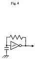
- FIG. 4is a functional block diagram of an exemplary oscillator.
- the single-wire communication bus for miniature low-power systems described as hereinfulfills the requirements mentioned above, and includes other enhancements pertaining to simplicity of use. It permits a slave to request service from the master unit by generating an interrupt using the same single wire.
- a single-wire serial communication bus(sometimes called “SWB”) according to the invention.
- a master 1may be seen as well as the single-wire bus 2 .
- a pull-up resistor 5is shown, about which more will be said later.
- Each device, master and slavehas an input device, such as a comparator or line receiver, permitting the device to learn whether the bus is at a high or low state.
- Each device, master and slavepreferably has a tri-state output device (line driver) permitting the device to pull the bus high or low.
- tri-state driversnamely drivers which are able to drive the bus actively to either of two states.
- tri-state driversin the idle state, the bus is lightly pulled-up or pulled-down, but during the transaction, the bus is driven hard to the appropriate state.
- a potential disadvantage of this approachis the possibility, however remote, of bus contention as mentioned above.
- the protocol devised for the bus according to the inventionis a protocol with a number of features that are intended to minimize or eliminate contention, and indeed these very features are what make possible the use of tri-state drivers and thus the above-described power savings and speed enhancement Stated differently, the design of the protocol described herein helps to save power and enhance speed, when compared with other protocols.
- single-wirein this context assumes a presence of a ground reference connection.
- the groundis provided by some other pin on each device and does not add to the pin count when used as a reference for this bus.
- single-wirein this context implies that only a single supplementary wire is required in addition to existing power and ground connections.
- Bus topologyThe bus topology, mentioned briefly above, will now be described in some detail.
- the single-wire communication bus 2includes at least a single master 1 and one slave 3 device.
- many slave 4 devicescan also be connected to the same bus 2 .
- the slave devicesmay sit in an “address space” of five bits, meaning there could be up to thirty-two distinct slave devices.
- each of the devices connected to the busshould have a pin dedicated to operations of the bus, with an input buffer (preferably interrupt-capable) and an output driver (with float/tri-state ability).
- a current source/sink or resistive device 5 with weak pull-up or pull-down capabilityshould also be present, either one per whole system, or included in one or all devices.
- the polarity of the interrupt signal and corresponding (opposing) connection of the pull-up/down mechanism 5should be the same for all of the units connected to the bus.
- the operations of the busare characterized by the absence of any requirement to have an accurate clock source at either master or slaves, as the required transmission speed is determined (calibrated) for each and every transaction from the bit pattern in the “Start Field.” So far as the master device is concerned, its clock must be stable, in the sense that it will generate clock pulses with very nearly constant period. But its clock need not be particularly accurate, in the sense that it could operate at one frequency for a particular transmission and at another frequency for another transmission. Likewise it could operate at a higher or lower frequency so long as every one of the slave devices is able to follow. For example, for the various slave devices each will have some upper limit as to how fast its own clock can run in response to the calibration pulses from the master. Clearly the master must confine its clock not to exceed the abilities of the slowest of the slave devices when considered according to their respective upper clock limits. The cumulative drift over the period of time for a bus message needs to be small, probably well less than one-half of a bit time.
- each slave deviceLikewise so far as each slave device is concerned, its clock must likewise be stable in the sense that it will generate clock pulses with very nearly constant period, with drift that is small enough that the cumulative drift over the period of time needed for a bus message will be small, probably well less than one-half of a bit time. In this way, even if the master is drifting “slow” and the slave device drifting “fast” (or vice versa), by the end of the bus message the clocking by the slave will nonetheless permit it to extract correct bus samples (of bits sent by the master) from the bus.
- Stopping clocksThose skilled in the art will be well aware that for many miniature products, the desire to maximize battery life leads to seemingly extreme measures such as shutting down oscillators whenever possible. This is because in many systems the oscillator or oscillators turn out to be among the chief battery drains. Of course this means that if a particular device within a product has had its oscillator halted, there is a need to get the oscillator restarted without undue delay at such time as the oscillator is again needed.
- each slave devicecan wait in a “sleep” state (that is, with its oscillator turned off) until there is activity on the line.
- the activityprompts each slave to pay close attention to the bit times at the beginning of the message from the master.
- the slavewill “synch” in the sense that will cause its oscillator to start and appropriate circuitry in the slave will do what is needed to arrive at-a clock signal that permits clocking in address and data information from the line.
- FIG. 4is an example of an oscillator that will restart immediately. It is not particularly accurate and is not particularly stable in the long run. In particular it is not particularly temperature-stable. It will be appreciated, however, that for the system according to the invention, the oscillator needs to be stable only for the duration of a single bus transaction, and in normal conditions the maximum temperature change during a particular bus transaction is quite small.
- the operations of the busare further designed in such a way that the conflict between the drivers on the master and one or more slaves (that assert the Interrupt signal) is prevented.
- a conflictmay occur when at least two drivers are trying to set the bus line to opposing states. The high supply currents resulting from such conflicts are highly undesirable in operation, and may also damage the individual master or slave units.
- the operations of the busare further characterized by aspects of the bus protocol according to which the bus transactions have predetermined and fixed duration. Stated differently, the bus transactions have a duration which does not depend on varying transmitted data and varying addressing information.
- slave devices 3 and 4can only receive and transmit data in reply to a transaction started by the master device 1 .
- the only signal which can be asserted by one or more slaves on their own (that is, in the absence of a transaction started by the master device 1 )is the interrupt signal, which is defined to be a pulse of limited duration.
- the busIn the system described here, most of the time the bus is in the idle state. In the idle state all drivers, in the master and in all slaves, are turned off (floating), and the pull-up device maintains the high logic state of the bus line. According to the protocol described here, before starring any transaction, the master and/or slave units observe the bus line, and wait for it to become idle, if necessary.
- Each transactionconsists of the following stages (see FIG. 2 and FIG. 3 ):
- All transactionare asynchronous, with equal bit time for each and every bit.
- the start stageshould have at least three (3) elements, but may be extended to an arbitrary number of bits. It will be appreciated that the number of bits in the start stage needs to be known to, or previously programmed into, each and every device on the bus.
- the start stageessentially consists of alternating high and low logical states of the bus, with each state having duration equal to a single bit time.
- the purpose of the start stageis to allow the determination (by each slave device) of the transmission speed and to synchronize the receiver (in each slave device) to the beginning of the message.
- the read or write intention determination stageuses several bits to convey to the slave device or devices the intentions of the master device.
- Several bitsare used to reduce the risk of a single incorrect bit changing the intended operation, and possibly creating the driver conflict condition, for example, a situation in which the master is trying to transmit information at the same time as a slave.
- the bit-pattern 0,1,1denotes a write transaction (master to slave)
- bit-pattern 1,1,0denotes a read transaction (slave to master). All other patterns are rejected as invalid, and the transaction is ignored.
- the addressing stageprovides the addresses for selection of individual devices connected to the Bus, as well as the addresses of various registers inside each of the device. Again, the number of address bits should be known (or set) in the master and all slave devices prior to operations. It is possible to operate some of the slaves with a lesser number of address bits, as long as the selection of each slave device can be made without ambiguity.
- An address field of five (5) bitsis illustrated in FIG. 2 and FIG. 3 .
- a particular addresscould be defined as a multicast address directed to all slave devices.
- some other particular addresscould be defined as a multicast address directed to particular ones of the slave devices, namely more than one and less than all of the slave devices. It will be appreciated that in the event of a multicast message it is not permitted for two or more slaves each to send an acklowledgment of receipt of the message, because such duplicate acknowledgments would risk collisions of bus data.
- the bus direction reassignment (turn-around) stageprovides an idle “slot” equal to the normal bit time, thus providing an interval for reversal of the information flow. It allows for the orderly and non-simultaneous disabling and enabling of the drivers on the master and slave devices. (in this context “non-simultaneous” means that there is no requirement that the disabling and enabling be simultaneous; the device that will transmit after the reversal has occurred can enable its driver slightly early or slightly late without risking an overlap with the “enabled” time of the driver for the device that was transmitting before the reversal occurred.)
- the turn-around stageappears in several positions during the transaction.
- the data stageis when the actual information is transferred.
- the number of bits in the data stagecan again be arbitrary, but needs to be known to the master and all slave units.
- a payload of eight (8) bitsis illustrated in FIG. 2 and FIG. 3 .
- the error detection stagefollows the data stage, and (in this exemplary embodiment) appends two parity bits at the end of the data stage.
- the second parity bitis simply an inverse of the first parity bit This prevents a permanently “stuck” line from indicating a correct parity for the message, no matter what data is transmitted.
- a specific parity value of 0,1is illustrated in FIG. 2 and FIG. 3 .
- the error detection and acknowledgment stageis only used in the write transactions, when the slave acknowledges the receipt of information and (in this embodiment) retransmits the parity bits from the original message. Again, a specific parity and acknowledgment value of 0,1 is illustrated in FIG. 2 .
- the stop stageenforces an idle condition on the Bus for some time after the transaction. It may do so for several bit times, the exact number known to both master and all slaves.
- a single-bit stop timeis illustrated in FIG. 2 and FIG. 3 .
- bits during the bus direction reassignment (turn-around) stage and stop stageare also called “guard” bits, since they guard against the possibly of creating the driver conflict condition where the master and a slave device attempt simultaneously to drive the bus to nonidentical levels.
- ParityIn the embodiment described here the system is able to discern whether a message has been accurately received by means of a parity check.
- the slave device receiving a messagewill calculate the parity of the message and will compare the calculated parity with the parity bit at the end of the message. Retransmission of the parity bit from the slave to the master permits the master to know that the slave has received the message.
- the operationis a “master read” operation, then the slave will calculate a parity, and will append it to the data which it is sending to the master.
- the masterthen calculates the parity and compares this with the parity at the end of the message. This permits the master to know that the message was correctly received.
- a device receiving a message having paritymay follow either of two approaches in confirming parity.
- One approachis to calculate the message parity for all the bits other than the parity bit itself, and then to compare the calculated parity with the received first parity bit. (Here, with a two-bit parity message, there is also a check made to be sure that the second parity message bit is of opposite sense from the first bit.)
- Another approachis to calculate the message parity for all of the message bits including the first parity bit, and to see if the cumulative parity is of the expected sense (e.g. even or odd).
- the cumulative parityis of the expected sense (e.g. even or odd).
- acknowledgementis meant to encompass a response that is a parity-bit response or a CRC response, with the type of response selected to match the needs of the system.
- the start stagemay be defined as three bit times, arbitrarily called a “prestart” bit, a “start” bit, and a “post-start” bit
- the prestart bithappens, this wakes up the slave and it starts its oscillator.
- the oscillatoris selected to be, for example, at least fifty-two times faster than the expected bit times for the bus transactions. By the time the start bit leading edge is detected, the oscillator has been running and stable for some number of oscillator cycles.
- the slavein an exemplary embodiment, counts its oscillator pulses from the leading edge of the start bit to the trailing edge of the start bit. This count is stored and is used by the slave during the rest of the bus transaction.
- the slavedetermines the bit starting and ending times for the remaining bits of the transaction by detecting and analyzing the bus states of the start stage. The slave then receives bits from the master according to the determined bit time and, if necessary, transmits bits to the master according to the determined bit time.
- the slaveuses the count to select sampling times that are intended to fall in the middle of each of the bit times of the transaction for the RW stage, the address stage, the data stage, and the parity stage. If the slave is supposed to send an acknowledgment, then the count is used to select the starting and ending times for the two bits of the acknowledgment.
- the slaveuses the count to select sampling times that are intended to fall in the middle of each of the bit times of the transaction for the RW stage and the address stage. If the slave is supposed to send a response, then the count is used to select the starting and ending times for the bits of the the data stage, and the parity stage.
- a common clockis being used by a particular slave as well as by the master.
- the slavecan use the common clock for determining the bit times.
- the bus transactionsare not, strictly speaking, asynchronous.
- the slavecan operate with as little as four clocks per bit time, and as little as two clocks per bit time for simple “write” transactions.
- a slave device's power budgetincludes the power used to operate its oscillator.
- “sleep”which, among other things, means its oscillator does not need to be running.
- the designer of a slave deviceis able to choose among several options in deciding when the slave can go to sleep. For example, in some applications for a write transaction (e.g. FIG. 2 ) a particular slave on the bus will remain awake long enough to calculate the parity, and will then go to sleep immediately thereafter if the address is not the address of the particular slave. Yet in other applications for a write transaction (e.g. FIG. 2 ) a particular slave on the bus will remain awake long enough to calculate the parity, and will then go to sleep immediately thereafter if the address is not the address of the particular slave. Yet in other applications for a write transaction (e.g. FIG.
- a particular slave on the buswill remain awake only long enough to receive the address, and will then go to sleep immediately thereafter if the address is not the address of the particular slave. (This saves energy to the oscillator during the data and parity stages, and saves the computational cost of computing the parity.)
- a particular slave on the busmay remain awake long enough to receive the address, and will then go to sleep immediately thereafter if the address is not the address of the particular slave.
- Determining the source of an interruptIt is instructive to consider what happens when a slave pulls an interrupt down.
- the masterat this point, merely knows that a slave pulled an interrupt down, but does not know which slave did so. In such a case, preferably the master polls the slaves and thus determines which slave generated the interrupt. In a simple case the master would poll the slaves seriatim based on the addressing system being used. In some systems, however, it may be known that the slaves differ in the urgency of servicing their interrupts in which case the master may poll first the slaves which (if they have an interrupt at all) have urgent interrupts.
- the system designermay not have control over all placement of devices on the bus, in which case it may prove necessary at some initial configuration time (e.g. at system power-up) to poll all possible bus addresses to develop a list of all slave devices that turn out to be present at the time of system power-up. It is then interesting to consider what would happen if a slave device were added to the bus after the initial polling-of-all-addresses. If that slave were to generate an interrupt, the master would have to repeat the polling-of-all-addresses to learn the address of the newly added slave device.
- the overhead associated with a polling-of-all-devicesneed not be prohibitive. In the example given here, there may be five address bits. This defines at most thirty-two slave devices, and thus only thirty-two polls would be needed to check for the presence or absence of each of the thirty-two possible devices.
- each of the deviceshas a mechanism for checking if the bus is free, before starting any transaction. (This mechanism simply checks to see if the bus is in its quiescent state.) It will be appreciated that for this to work well, the bus must in its entirety be short in length as compared with the distance that light would travel during a bit time. Stated differently, if a master and slave were on a very long bus, then one device might sample the bus to see if it is free, only to have a pulse arrive from the other end of the bus at an inconvenient moment, part way through an attempted bus transaction. In the typical battery-powered appliances described above (e.g.
- the form factor of the applianceimposes a natural upper bound on the length of the bus, e.g. much shorter than one meter, and this means that a pulse from the other end of the bus will not take very long to arrive.
- each slavewill be designed so that it recognizes that its interrupt is lost (e.g. by monitoring the bus and noting that its interrupt is badly formed). In that event, the slave activates its interrupt again some short time after the current transaction is finished.
- each slave that determines that it needs to have an interrupt servicedwill set a bit in an appropriate internal register. This bit is indicative of the need to have an interrupt serviced.
- the slaveWith such a slave, the slave retransmits the lost or unserviced interrupt after every bus transaction until the interrupt is specifically cleared in the appropriate internal register.
- the masterhaving serviced the interrupt, sends a message to the slave telling it to clear the bit. Ideally the master would send such a message right away after servicing the interrupt, although in some situations where the master is needed for other tasks, the clearing might have to wait until the master is not so busy.
- This approachhas the possible drawback that it may use up bus bandwidth due to the sending of a large number of otherwise unnecessary duplicate interrupts, for example in situation where the interrupt request bit is specifically not cleared to save time.
- this capabilitymay be programmable.
- the masteror other equipment external to the slave
- the slavewill be able to choose whether to enable the “extra” interrupt pulses (which reduces the risk of a lost interrupt) or to disable the “extra” interrupt pulses (which reduces the risk of wasted bus bandwidth).
- the slavemay be programmable as to how often it generates an interrupt when its flag is set, e.g. no more often than an interval defined as some number of miliseconds, or no more often than every second or third bus transaction.
- a slavemay be configured so as to prioritize its own interrupt events. Certain interrupt events might prompt the slave to generate only a single interrupt, while other interrupt events might prompt the slave to generate repeated interrupts until cleared.
- the master and slavescould be configured so that a particular multicast message is understood as a query to all of the slaves as to whether any of the slaves happens to have an uncleared interrupt.
- the mastercould transmit this multicast message from time to time so as to catch any uncleared interrupts.
Landscapes
- Engineering & Computer Science (AREA)
- Computer Networks & Wireless Communication (AREA)
- Signal Processing (AREA)
- Information Transfer Systems (AREA)
- Synchronisation In Digital Transmission Systems (AREA)
Abstract
Description
- Power consumption. When a logic state opposite to the pull-up/pull-down is transmitted, there will be current expended, for the duration of one bit time. This current could be quite significant if a high data rate is desired. It leads for example to power dissipation in the pull-up/pull-down resistor for the duration of the logic state.
- Speed. Bus capacitance in combination with the resistive pull-up/pull-down device will follow a simple RC time constant as the bus line recharges to the inactive state. This fact has been known to create problems in existing busses such as that described in the above-mentioned U.S. Pat. No. 4,689,740, when they are operated at any but the slowest of speeds.
- Start;
- Read or Write intention determination;
- Addressing;
- Bus direction reassignment (turn-around), if required;
- Data;
- Error Detection;
- Bus direction reassignment (turn-around), if required;
- Error detection and acknowledgement, and
- Stop.
Claims (44)
Priority Applications (1)
| Application Number | Priority Date | Filing Date | Title |
|---|---|---|---|
| US10/480,757US7519005B2 (en) | 2002-05-08 | 2003-04-28 | Single-wire communication bus for miniature low-power systems |
Applications Claiming Priority (3)
| Application Number | Priority Date | Filing Date | Title |
|---|---|---|---|
| US37937402P | 2002-05-08 | 2002-05-08 | |
| US10/480,757US7519005B2 (en) | 2002-05-08 | 2003-04-28 | Single-wire communication bus for miniature low-power systems |
| PCT/US2003/012959WO2003096036A1 (en) | 2002-05-08 | 2003-04-28 | Single-wire communication bus for miniature low-power systems |
Publications (2)
| Publication Number | Publication Date |
|---|---|
| US20040208200A1 US20040208200A1 (en) | 2004-10-21 |
| US7519005B2true US7519005B2 (en) | 2009-04-14 |
Family
ID=29420521
Family Applications (1)
| Application Number | Title | Priority Date | Filing Date |
|---|---|---|---|
| US10/480,757Active2026-01-06US7519005B2 (en) | 2002-05-08 | 2003-04-28 | Single-wire communication bus for miniature low-power systems |
Country Status (3)
| Country | Link |
|---|---|
| US (1) | US7519005B2 (en) |
| AU (1) | AU2003225172A1 (en) |
| WO (1) | WO2003096036A1 (en) |
Cited By (33)
| Publication number | Priority date | Publication date | Assignee | Title |
|---|---|---|---|---|
| US20060031618A1 (en)* | 2004-05-20 | 2006-02-09 | Hansquine David W | Single wire and three wire bus interoperability |
| US20090193165A1 (en)* | 2008-01-30 | 2009-07-30 | Hon Hai Precision Industry Co., Ltd. | Communication circuit of serial peripheral interface devices |
| US20090300247A1 (en)* | 2008-05-30 | 2009-12-03 | Wen-Hsia Kung | Interface transmission device and method |
| US20100023663A1 (en)* | 2008-07-24 | 2010-01-28 | Diehl Aerospace Gmbh | Method and device for detecting bus subscribers |
| US20100064074A1 (en)* | 2004-05-20 | 2010-03-11 | Qualcomm Incorporated | Single wire bus interface |
| US20110122978A1 (en)* | 2008-05-30 | 2011-05-26 | Continental Teves Ag & Co, Ohg | Serial peripheral interface having a reduced number of connecting lines |
| US20120106663A1 (en)* | 2010-11-02 | 2012-05-03 | O2Micro, Inc. | Method for transmitting data |
| US20120144078A1 (en)* | 2010-12-02 | 2012-06-07 | Research In Motion Limited | Single wire bus system |
| CN102591834A (en)* | 2010-12-02 | 2012-07-18 | 捷讯研究有限公司 | Single wire bus system |
| US20140365697A1 (en)* | 2012-02-24 | 2014-12-11 | Panasonic Corporation | Slave device, master device, communication system, and communication method |
| US9252900B2 (en) | 2012-06-01 | 2016-02-02 | Blackberry Limited | Universal synchronization engine based on probabilistic methods for guarantee of lock in multiformat audio systems |
| US9312400B2 (en) | 2011-07-01 | 2016-04-12 | Tyco Electronics Corporation | Power harvesting device |
| US9461812B2 (en) | 2013-03-04 | 2016-10-04 | Blackberry Limited | Increased bandwidth encoding scheme |
| US9473876B2 (en) | 2014-03-31 | 2016-10-18 | Blackberry Limited | Method and system for tunneling messages between two or more devices using different communication protocols |
| US9479275B2 (en) | 2012-06-01 | 2016-10-25 | Blackberry Limited | Multiformat digital audio interface |
| US9490999B2 (en) | 2015-01-28 | 2016-11-08 | Atmel Corporation | Single-wire communications using iterative baud learning |
| US9652431B2 (en) | 2015-01-26 | 2017-05-16 | Atmel Corporation | Single wire communications using predictive host sampling window |
| US9699863B2 (en) | 2014-05-30 | 2017-07-04 | Lutron Electronics Co., Inc. | Multiple location load control system |
| US9755821B2 (en) | 2015-04-02 | 2017-09-05 | Samsung Electronics Co., Ltd. | Device including single wire interface and data processing system including the same |
| US9772210B1 (en) | 2012-06-11 | 2017-09-26 | Brian L. Houghton | Storage tank level detection method and system |
| US20180032457A1 (en)* | 2016-07-26 | 2018-02-01 | Qualcomm Incorporated | Slave initiated interrupts for a communication bus |
| US10133692B2 (en) | 2015-08-24 | 2018-11-20 | Samsung Electronics Co., Ltd. | Device including a single wire interface and a data processing system having the same |
| US20190215100A1 (en)* | 2016-05-18 | 2019-07-11 | Sony Semiconductor Solutions Corporation | Communication apparatus, communication method, program, and communication system |
| US10983942B1 (en) | 2019-12-11 | 2021-04-20 | Qorvo Us, Inc. | Multi-master hybrid bus apparatus |
| US11018788B2 (en)* | 2015-12-04 | 2021-05-25 | Infineon Technologies Ag | Robust high speed sensor interface for remote sensors |
| US11106615B2 (en) | 2019-01-16 | 2021-08-31 | Qorvo Us, Inc. | Single-wire bus (SuBUS) slave circuit and related apparatus |
| US11119958B2 (en) | 2019-04-18 | 2021-09-14 | Qorvo Us, Inc. | Hybrid bus apparatus |
| US11226924B2 (en)* | 2019-04-24 | 2022-01-18 | Qorvo Us, Inc. | Single-wire bus apparatus supporting slave-initiated operation in a master circuit |
| US11409677B2 (en) | 2020-11-11 | 2022-08-09 | Qorvo Us, Inc. | Bus slave circuit and related single-wire bus apparatus |
| US11489695B2 (en) | 2020-11-24 | 2022-11-01 | Qorvo Us, Inc. | Full-duplex communications over a single-wire bus |
| US11706048B1 (en) | 2021-12-16 | 2023-07-18 | Qorvo Us, Inc. | Multi-protocol bus circuit |
| US12092689B2 (en) | 2021-12-08 | 2024-09-17 | Qorvo Us, Inc. | Scan test in a single-wire bus circuit |
| US12182052B2 (en) | 2022-01-20 | 2024-12-31 | Qorvo Us, Inc. | Slave-initiated communications over a single-wire bus |
Families Citing this family (39)
| Publication number | Priority date | Publication date | Assignee | Title |
|---|---|---|---|---|
| US7116739B1 (en) | 2002-10-31 | 2006-10-03 | Zilog, Inc. | Auto baud system and method and single pin communication interface |
| US7406100B2 (en)* | 2003-05-21 | 2008-07-29 | Atmel Corporation | Bi-directional single wire interface |
| US7606955B1 (en)* | 2003-09-15 | 2009-10-20 | National Semiconductor Corporation | Single wire bus for connecting devices and methods of operating the same |
| US7127538B1 (en) | 2004-05-21 | 2006-10-24 | Zilog, Inc. | Single-pin serial communication link with start-bit flow control |
| US7260660B1 (en) | 2004-05-21 | 2007-08-21 | Zilog, Inc. | Flow control by supplying a remote start bit onto a single-wire bus |
| US7895301B1 (en) | 2004-05-21 | 2011-02-22 | Uei Cayman Inc. | Transmitting a codeset over a single-wire bus from a computer to a remote control device |
| CN1790990B (en)* | 2004-12-17 | 2010-04-14 | 华为技术有限公司 | Asynchronous serial bus communication method and slave node based on address space access |
| DE102005060025A1 (en)* | 2005-12-15 | 2007-06-21 | Siemens Ag | Method for transmitting information by means of pulse diagnosis modulating pulse width modulation |
| CN101375642B (en)* | 2006-01-30 | 2015-12-16 | 皇家飞利浦电子股份有限公司 | Lighting Control Assembly |
| US7288962B2 (en)* | 2006-02-08 | 2007-10-30 | Kyocera Wireless Corp. | Level shifting multiplexing circuit for connecting a two conductor full duplex bus to a bidirectional single conductor bus |
| DE102006060081B3 (en)* | 2006-12-19 | 2008-06-19 | Infineon Technologies Ag | Communication device for communication after master slave communication instruction, is formed as slave instance which communicates over bus with master instance |
| DE102007041874A1 (en)* | 2007-09-04 | 2009-03-26 | Giesecke & Devrient Gmbh | Data communication according to the single-wire protocol |
| US7788430B2 (en) | 2007-09-14 | 2010-08-31 | Microchip Technology Incorporated | Enhanced single-node protocol for data, address and control operations |
| US20090080442A1 (en)* | 2007-09-26 | 2009-03-26 | Narayan Ananth S | Conserving power in a multi-node environment |
| NL2001722C2 (en)* | 2008-06-25 | 2009-12-29 | Ascom Sweden Ab | Nurse call system for use in e.g. hospital, for communication between patient and medical staff, has communication ports connected with electric wires, and message unit arranged to communicate system with chamber-controller over wires |
| DE102008031357B4 (en) | 2008-07-04 | 2017-06-29 | Sennheiser Electronic Gmbh & Co. Kg | Method and system for the serial transmission of data |
| DE102009046995A1 (en) | 2008-11-21 | 2010-05-27 | Continental Teves Ag & Co. Ohg | Data transfer protocol |
| US8291143B1 (en)* | 2009-02-11 | 2012-10-16 | Brocade Communication Systems, Inc. | Single line communication |
| US8176310B2 (en)* | 2009-06-19 | 2012-05-08 | Phoenix Technologies Ltd. | Debugger application configured to communicate with a debugger module via a GPIO |
| FR2948474A1 (en)* | 2009-07-22 | 2011-01-28 | Proton World Int Nv | COMMUNICATION PROTOCOL ON A UNIFIL BUS |
| EP2391095A1 (en)* | 2010-05-31 | 2011-11-30 | Fluke Corporation | Automatic addressing scheme for 2 wire serial bus interface |
| FR2963449B1 (en)* | 2010-07-27 | 2013-01-25 | St Microelectronics Rousset | CONVERSION OF A BIFILAR BUS IN A UNIFIL BUS |
| FR2963519B1 (en) | 2010-07-27 | 2012-08-03 | St Microelectronics Rousset | COMMUNICATION PROTOCOL ON A UNIFIL BUS |
| FR2963451B1 (en) | 2010-07-27 | 2012-12-07 | St Microelectronics Rousset | AUTHENTICATION OF MULTIPROTOCOL COMMUNICATION |
| FR2967816A1 (en)* | 2010-11-19 | 2012-05-25 | Commissariat Energie Atomique | METHOD AND DEVICE FOR ASYNCHRONOUS DATA COMMUNICATION ON A SINGLE DRIVER |
| US20130019039A1 (en)* | 2011-06-10 | 2013-01-17 | Intersil Americas LLC | System and method for operating a one-wire protocol slave in a two-wire protocol bus environment |
| WO2013185111A2 (en) | 2012-06-07 | 2013-12-12 | Apple Inc. | Methods and apparatus for synchronization among integrated circuits within a wireless network |
| DE102012014485A1 (en)* | 2012-07-23 | 2014-05-15 | Sew-Eurodrive Gmbh & Co Kg | Registration method and bus communication device |
| US9910819B2 (en)* | 2013-03-11 | 2018-03-06 | Microchip Technology Incorporated | Two-wire serial interface and protocol |
| EP2948858B1 (en)* | 2013-03-15 | 2018-06-06 | Apple Inc. | Method and apparatus for multi-drop digital bus |
| US10085224B2 (en) | 2014-11-19 | 2018-09-25 | Apple Inc. | Methods and apparatus for synchronization of media playback within a wireless network |
| US9946677B2 (en)* | 2015-02-12 | 2018-04-17 | Atmel Corporation | Managing single-wire communications |
| DE102016100845B3 (en)* | 2016-01-19 | 2017-03-16 | Elmos Semiconductor Aktiengesellschaft | Bus interface for a bidirectional single-wire light control bus |
| EP3405804B1 (en) | 2016-01-19 | 2021-03-24 | Elmos Semiconductor SE | Jtag interfaces for controlling the actuation device of lighting means or a lighting chain |
| DE102016100843B3 (en)* | 2016-01-19 | 2017-03-02 | Elmos Semiconductor Aktiengesellschaft | Single wire data bus with several bus nodes |
| DE102016123400B3 (en) | 2016-01-19 | 2017-04-06 | Elmos Semiconductor Aktiengesellschaft | Single-wire light control bus with several levels |
| US10212658B2 (en)* | 2016-09-30 | 2019-02-19 | Kinetic Technologies | Systems and methods for managing communication between devices |
| US10135634B2 (en)* | 2016-11-03 | 2018-11-20 | Infineon Technologies Ag | Bus interface with bi-directional, one-wire communication and individual select lines |
| US10757484B2 (en) | 2017-01-05 | 2020-08-25 | Kinetic Technologies | Systems and methods for pulse-based communication |
Citations (12)
| Publication number | Priority date | Publication date | Assignee | Title |
|---|---|---|---|---|
| US4689740A (en) | 1980-10-31 | 1987-08-25 | U.S. Philips Corporation | Two-wire bus-system comprising a clock wire and a data wire for interconnecting a number of stations |
| US5237322A (en)* | 1990-12-08 | 1993-08-17 | Deutsche Itt Industries Gmbh | Master-slave data transmission system employing a flexible single-wire bus |
| US5321818A (en)* | 1992-05-12 | 1994-06-14 | Hughes Aircraft Company | System for arbitrating for access on VME bus structures |
| US5412644A (en) | 1992-09-16 | 1995-05-02 | Deutsche Itt Industries Gmbh | Serial bus system with a single-wire line |
| US5579299A (en) | 1994-12-16 | 1996-11-26 | Chrysler Corporation | Communications network, a dual mode data transfer system therefor |
| US5761697A (en)* | 1990-11-19 | 1998-06-02 | Dallas Semiconductor Corporation | Identifiable modules on a serial bus system and corresponding identification methods |
| US5864872A (en) | 1989-05-15 | 1999-01-26 | Dallas Semiconductor Corporation | Single wire communication system |
| US6065824A (en) | 1994-12-22 | 2000-05-23 | Hewlett-Packard Company | Method and apparatus for storing information on a replaceable ink container |
| US6298066B1 (en) | 1999-04-14 | 2001-10-02 | Maxim Integrated Products, Inc. | Single wire bus interface for multidrop applications |
| US6412072B2 (en) | 1995-07-20 | 2002-06-25 | Dallas Semiconductor Corporation | Parasitically powered microprocessor capable of transmitting data over a single data line and ground |
| US6501342B2 (en) | 2000-01-28 | 2002-12-31 | Semtech Corporation | Power-conserving external clock for use with a clock-dependent integrated circuit |
| US20030149819A1 (en)* | 2002-02-06 | 2003-08-07 | Smith Robert B. | Method and apparatus for ascertaining the status of multiple devices simultaneously over a data bus |
- 2003
- 2003-04-28USUS10/480,757patent/US7519005B2/enactiveActive
- 2003-04-28WOPCT/US2003/012959patent/WO2003096036A1/ennot_activeApplication Discontinuation
- 2003-04-28AUAU2003225172Apatent/AU2003225172A1/ennot_activeAbandoned
Patent Citations (14)
| Publication number | Priority date | Publication date | Assignee | Title |
|---|---|---|---|---|
| US4689740A (en) | 1980-10-31 | 1987-08-25 | U.S. Philips Corporation | Two-wire bus-system comprising a clock wire and a data wire for interconnecting a number of stations |
| US6108751A (en) | 1989-05-15 | 2000-08-22 | Dallas Semiconductor Corporation | Single wire data communication method |
| US5864872A (en) | 1989-05-15 | 1999-01-26 | Dallas Semiconductor Corporation | Single wire communication system |
| US5761697A (en)* | 1990-11-19 | 1998-06-02 | Dallas Semiconductor Corporation | Identifiable modules on a serial bus system and corresponding identification methods |
| US5495240A (en) | 1990-12-08 | 1996-02-27 | Deutsche Itt Industries Gmbh | Master-slave data transmission system employing a flexible single-wire bus |
| US5237322A (en)* | 1990-12-08 | 1993-08-17 | Deutsche Itt Industries Gmbh | Master-slave data transmission system employing a flexible single-wire bus |
| US5321818A (en)* | 1992-05-12 | 1994-06-14 | Hughes Aircraft Company | System for arbitrating for access on VME bus structures |
| US5412644A (en) | 1992-09-16 | 1995-05-02 | Deutsche Itt Industries Gmbh | Serial bus system with a single-wire line |
| US5579299A (en) | 1994-12-16 | 1996-11-26 | Chrysler Corporation | Communications network, a dual mode data transfer system therefor |
| US6065824A (en) | 1994-12-22 | 2000-05-23 | Hewlett-Packard Company | Method and apparatus for storing information on a replaceable ink container |
| US6412072B2 (en) | 1995-07-20 | 2002-06-25 | Dallas Semiconductor Corporation | Parasitically powered microprocessor capable of transmitting data over a single data line and ground |
| US6298066B1 (en) | 1999-04-14 | 2001-10-02 | Maxim Integrated Products, Inc. | Single wire bus interface for multidrop applications |
| US6501342B2 (en) | 2000-01-28 | 2002-12-31 | Semtech Corporation | Power-conserving external clock for use with a clock-dependent integrated circuit |
| US20030149819A1 (en)* | 2002-02-06 | 2003-08-07 | Smith Robert B. | Method and apparatus for ascertaining the status of multiple devices simultaneously over a data bus |
Cited By (54)
| Publication number | Priority date | Publication date | Assignee | Title |
|---|---|---|---|---|
| US20100064074A1 (en)* | 2004-05-20 | 2010-03-11 | Qualcomm Incorporated | Single wire bus interface |
| US8750324B2 (en)* | 2004-05-20 | 2014-06-10 | Qualcomm Incorporated | Single wire bus interface |
| US20060031618A1 (en)* | 2004-05-20 | 2006-02-09 | Hansquine David W | Single wire and three wire bus interoperability |
| US20090193165A1 (en)* | 2008-01-30 | 2009-07-30 | Hon Hai Precision Industry Co., Ltd. | Communication circuit of serial peripheral interface devices |
| US7603501B2 (en)* | 2008-01-30 | 2009-10-13 | Hon Hai Precsion Industry Co., Ltd. | Communication circuit of serial peripheral interface devices |
| US20110122978A1 (en)* | 2008-05-30 | 2011-05-26 | Continental Teves Ag & Co, Ohg | Serial peripheral interface having a reduced number of connecting lines |
| US8161216B2 (en)* | 2008-05-30 | 2012-04-17 | Realtek Semiconductor Corp. | Interface transmission device and method |
| US20090300247A1 (en)* | 2008-05-30 | 2009-12-03 | Wen-Hsia Kung | Interface transmission device and method |
| US9042274B2 (en) | 2008-05-30 | 2015-05-26 | Continental Teves Ag & Co. Ohg | Serial peripheral interface having a reduced number of connecting lines |
| US8117366B2 (en)* | 2008-07-24 | 2012-02-14 | Diehl Aerospace Gmbh | Method and device for detecting locations of bus subscribers |
| US20100023663A1 (en)* | 2008-07-24 | 2010-01-28 | Diehl Aerospace Gmbh | Method and device for detecting bus subscribers |
| US20120106663A1 (en)* | 2010-11-02 | 2012-05-03 | O2Micro, Inc. | Method for transmitting data |
| US20120144078A1 (en)* | 2010-12-02 | 2012-06-07 | Research In Motion Limited | Single wire bus system |
| CN102591834A (en)* | 2010-12-02 | 2012-07-18 | 捷讯研究有限公司 | Single wire bus system |
| US8775707B2 (en)* | 2010-12-02 | 2014-07-08 | Blackberry Limited | Single wire bus system |
| US10007637B2 (en) | 2010-12-02 | 2018-06-26 | Blackberry Limited | Single wire bus system |
| US9312400B2 (en) | 2011-07-01 | 2016-04-12 | Tyco Electronics Corporation | Power harvesting device |
| US20140365697A1 (en)* | 2012-02-24 | 2014-12-11 | Panasonic Corporation | Slave device, master device, communication system, and communication method |
| US9378166B2 (en)* | 2012-02-24 | 2016-06-28 | Panasonic Intellectual Property Management Co., Ltd. | Slave device, master device, communication system, and communication method |
| US9479275B2 (en) | 2012-06-01 | 2016-10-25 | Blackberry Limited | Multiformat digital audio interface |
| US9252900B2 (en) | 2012-06-01 | 2016-02-02 | Blackberry Limited | Universal synchronization engine based on probabilistic methods for guarantee of lock in multiformat audio systems |
| US9672177B2 (en) | 2012-06-01 | 2017-06-06 | Blackberry Limited | Synchronization of electronic device with another electronic device on bus using synchronization field |
| US9772210B1 (en) | 2012-06-11 | 2017-09-26 | Brian L. Houghton | Storage tank level detection method and system |
| US9461812B2 (en) | 2013-03-04 | 2016-10-04 | Blackberry Limited | Increased bandwidth encoding scheme |
| US9473876B2 (en) | 2014-03-31 | 2016-10-18 | Blackberry Limited | Method and system for tunneling messages between two or more devices using different communication protocols |
| US9699863B2 (en) | 2014-05-30 | 2017-07-04 | Lutron Electronics Co., Inc. | Multiple location load control system |
| US11094353B2 (en) | 2014-05-30 | 2021-08-17 | Lutron Technology Company Llc | Multiple location load control system |
| US12402219B2 (en) | 2014-05-30 | 2025-08-26 | Lutron Technology Company Llc | Multiple location load control system |
| US10129948B2 (en) | 2014-05-30 | 2018-11-13 | Lutron Electronics Co., Inc. | Multiple location load control system |
| US12016094B2 (en) | 2014-05-30 | 2024-06-18 | Lutron Technology Company Llc | Multiple location load control system |
| US11558939B2 (en) | 2014-05-30 | 2023-01-17 | Lutron Technology Company Llc | Multiple location load control system |
| US10593373B2 (en) | 2014-05-30 | 2020-03-17 | Lutron Technology Company Llc | Multiple location load control system |
| US9652431B2 (en) | 2015-01-26 | 2017-05-16 | Atmel Corporation | Single wire communications using predictive host sampling window |
| US9882738B2 (en) | 2015-01-28 | 2018-01-30 | Atmel Corporation | Single-wire communications using iterative baud learning |
| US9490999B2 (en) | 2015-01-28 | 2016-11-08 | Atmel Corporation | Single-wire communications using iterative baud learning |
| US9882711B1 (en) | 2015-04-02 | 2018-01-30 | Samsung Electronics Co., Ltd. | Device including single wire interface and data processing system including the same |
| US9755821B2 (en) | 2015-04-02 | 2017-09-05 | Samsung Electronics Co., Ltd. | Device including single wire interface and data processing system including the same |
| US10133692B2 (en) | 2015-08-24 | 2018-11-20 | Samsung Electronics Co., Ltd. | Device including a single wire interface and a data processing system having the same |
| US11018788B2 (en)* | 2015-12-04 | 2021-05-25 | Infineon Technologies Ag | Robust high speed sensor interface for remote sensors |
| US11728916B2 (en) | 2015-12-04 | 2023-08-15 | Infineon Technologies Ag | Robust high speed sensor interface for remote sensors |
| US20190215100A1 (en)* | 2016-05-18 | 2019-07-11 | Sony Semiconductor Solutions Corporation | Communication apparatus, communication method, program, and communication system |
| US10721022B2 (en)* | 2016-05-18 | 2020-07-21 | Sony Semiconductor Solutions Corporation | Communication apparatus, communication method, program, and communication system |
| US20180032457A1 (en)* | 2016-07-26 | 2018-02-01 | Qualcomm Incorporated | Slave initiated interrupts for a communication bus |
| CN109479021B (en)* | 2016-07-26 | 2021-04-20 | 高通股份有限公司 | Slave initiated interrupts for a communication bus |
| CN109479021A (en)* | 2016-07-26 | 2019-03-15 | 高通股份有限公司 | The interruption that slave equipment for communication bus is initiated |
| US11106615B2 (en) | 2019-01-16 | 2021-08-31 | Qorvo Us, Inc. | Single-wire bus (SuBUS) slave circuit and related apparatus |
| US11119958B2 (en) | 2019-04-18 | 2021-09-14 | Qorvo Us, Inc. | Hybrid bus apparatus |
| US11226924B2 (en)* | 2019-04-24 | 2022-01-18 | Qorvo Us, Inc. | Single-wire bus apparatus supporting slave-initiated operation in a master circuit |
| US10983942B1 (en) | 2019-12-11 | 2021-04-20 | Qorvo Us, Inc. | Multi-master hybrid bus apparatus |
| US11409677B2 (en) | 2020-11-11 | 2022-08-09 | Qorvo Us, Inc. | Bus slave circuit and related single-wire bus apparatus |
| US11489695B2 (en) | 2020-11-24 | 2022-11-01 | Qorvo Us, Inc. | Full-duplex communications over a single-wire bus |
| US12092689B2 (en) | 2021-12-08 | 2024-09-17 | Qorvo Us, Inc. | Scan test in a single-wire bus circuit |
| US11706048B1 (en) | 2021-12-16 | 2023-07-18 | Qorvo Us, Inc. | Multi-protocol bus circuit |
| US12182052B2 (en) | 2022-01-20 | 2024-12-31 | Qorvo Us, Inc. | Slave-initiated communications over a single-wire bus |
Also Published As
| Publication number | Publication date |
|---|---|
| WO2003096036A1 (en) | 2003-11-20 |
| US20040208200A1 (en) | 2004-10-21 |
| AU2003225172A1 (en) | 2003-11-11 |
Similar Documents
| Publication | Publication Date | Title |
|---|---|---|
| US7519005B2 (en) | Single-wire communication bus for miniature low-power systems | |
| US6823224B2 (en) | Data processing system having an on-chip background debug system and method therefor | |
| US6049885A (en) | Method and apparatus for allowing a remote node to awaken a sleeping node of a network | |
| US4628480A (en) | Arrangement for optimized utilization of I/O pins | |
| USRE44270E1 (en) | System for providing access of multiple data buffers to a data retaining and processing device | |
| EP0140814B1 (en) | Power-conserving control system | |
| US7729427B2 (en) | Pseudo-synchronous one wire bidirectional bus interface | |
| EP4137955B1 (en) | Slave-to-slave direct communication | |
| US7565457B2 (en) | Serial advanced technology attachment device presence detection and hot-plug in low power mode | |
| JP3509232B2 (en) | Computer system and its power management device | |
| WO2017027417A1 (en) | Dynamic data-link selection over common physical interface | |
| JPH0511898A (en) | Peripheral controller and SCSI bus controller | |
| CN112639753A (en) | Aggregated inband interruption | |
| WO2007036801A2 (en) | Power conservation | |
| US8010818B2 (en) | Power efficient method for controlling an oscillator in a low power synchronous system with an asynchronous I2C bus | |
| CA1210827A (en) | Debounce circuit providing synchronously clocked digital signals | |
| US6946886B2 (en) | Clock-synchronized serial communication device and semiconductor integrated circuit device | |
| US6874047B1 (en) | System and method for implementing an SMBus/I2C interface on a network interface card | |
| US7437448B1 (en) | Method and device for function selection of a control unit | |
| CN117271397B (en) | General input/output circuit, general input/output circuit control method and chip | |
| JPH06152695A (en) | Serial interface circuit | |
| US6426953B1 (en) | Method of operating an internal high speed ATM bus inside a switching core | |
| CN114356815B (en) | USB controller, chip, display device and control method | |
| CN112214246A (en) | Low-power-consumption multiprocessor serial port awakening method and system | |
| JP2006053949A (en) | Storage device |
Legal Events
| Date | Code | Title | Description |
|---|---|---|---|
| AS | Assignment | Owner name:SEMTECH CORP., CALIFORNIA Free format text:ASSIGNMENT OF ASSIGNORS INTEREST;ASSIGNORS:HEJDEMAN, CARL;MARTEN, VICTOR;MCKNIGHT, ANDREW;REEL/FRAME:014377/0307;SIGNING DATES FROM 20030603 TO 20030616 | |
| FEPP | Fee payment procedure | Free format text:PAYOR NUMBER ASSIGNED (ORIGINAL EVENT CODE: ASPN); ENTITY STATUS OF PATENT OWNER: LARGE ENTITY | |
| STCF | Information on status: patent grant | Free format text:PATENTED CASE | |
| FPAY | Fee payment | Year of fee payment:4 | |
| AS | Assignment | Owner name:HSBC BANK USA, NATIONAL ASSOCIATION, NEW YORK Free format text:SECURITY AGREEMENT;ASSIGNORS:SEMTECH CORPORATION;SEMTECH NEW YORK CORPORATION;SIERRA MONOLITHICS, INC.;REEL/FRAME:030341/0099 Effective date:20130502 | |
| FPAY | Fee payment | Year of fee payment:8 | |
| AS | Assignment | Owner name:HSBC BANK USA, NATIONAL ASSOCIATION, AS ADMINISTRATIVE AGENT, CALIFORNIA Free format text:SECURITY INTEREST;ASSIGNORS:SEMTECH CORPORATION;SEMTECH NEW YORK CORPORATION;SIERRA MONOLITHICS, INC.;AND OTHERS;SIGNING DATES FROM 20151115 TO 20161115;REEL/FRAME:040646/0799 Owner name:HSBC BANK USA, NATIONAL ASSOCIATION, AS ADMINISTRA Free format text:SECURITY INTEREST;ASSIGNORS:SEMTECH CORPORATION;SEMTECH NEW YORK CORPORATION;SIERRA MONOLITHICS, INC.;AND OTHERS;SIGNING DATES FROM 20151115 TO 20161115;REEL/FRAME:040646/0799 | |
| MAFP | Maintenance fee payment | Free format text:PAYMENT OF MAINTENANCE FEE, 12TH YEAR, LARGE ENTITY (ORIGINAL EVENT CODE: M1553); ENTITY STATUS OF PATENT OWNER: LARGE ENTITY Year of fee payment:12 | |
| AS | Assignment | Owner name:JPMORGAN CHASE BANK, N.A., AS SUCCESSOR AGENT, ILLINOIS Free format text:ASSIGNMENT OF PATENT SECURITY INTEREST PREVIOUSLY RECORDED AT REEL/FRAME (040646/0799);ASSIGNOR:HSBC BANK USA, NATIONAL ASSOCIATION, AS RESIGNING AGENT;REEL/FRAME:062781/0544 Effective date:20230210 |