US7518429B2 - Delay circuit - Google Patents
Delay circuitDownload PDFInfo
- Publication number
- US7518429B2 US7518429B2US11/767,478US76747807AUS7518429B2US 7518429 B2US7518429 B2US 7518429B2US 76747807 AUS76747807 AUS 76747807AUS 7518429 B2US7518429 B2US 7518429B2
- Authority
- US
- United States
- Prior art keywords
- terminal
- resistor
- transistor
- circuit
- capacitor
- Prior art date
- Legal status (The legal status is an assumption and is not a legal conclusion. Google has not performed a legal analysis and makes no representation as to the accuracy of the status listed.)
- Expired - Fee Related
Links
- 239000003990capacitorSubstances0.000claimsabstractdescription27
- 238000007599dischargingMethods0.000claimsabstractdescription13
- 230000003111delayed effectEffects0.000claimsdescription4
- 230000001360synchronised effectEffects0.000claims1
- 238000010586diagramMethods0.000description4
Images


Classifications
- H—ELECTRICITY
- H03—ELECTRONIC CIRCUITRY
- H03H—IMPEDANCE NETWORKS, e.g. RESONANT CIRCUITS; RESONATORS
- H03H11/00—Networks using active elements
- H03H11/02—Multiple-port networks
- H03H11/26—Time-delay networks
- H—ELECTRICITY
- H03—ELECTRONIC CIRCUITRY
- H03K—PULSE TECHNIQUE
- H03K4/00—Generating pulses having essentially a finite slope or stepped portions
- H03K4/06—Generating pulses having essentially a finite slope or stepped portions having triangular shape
- H03K4/08—Generating pulses having essentially a finite slope or stepped portions having triangular shape having sawtooth shape
- H03K4/48—Generating pulses having essentially a finite slope or stepped portions having triangular shape having sawtooth shape using as active elements semiconductor devices
- H03K4/50—Generating pulses having essentially a finite slope or stepped portions having triangular shape having sawtooth shape using as active elements semiconductor devices in which a sawtooth voltage is produced across a capacitor
- H—ELECTRICITY
- H03—ELECTRONIC CIRCUITRY
- H03K—PULSE TECHNIQUE
- H03K5/00—Manipulating of pulses not covered by one of the other main groups of this subclass
- H03K5/01—Shaping pulses
- H03K5/04—Shaping pulses by increasing duration; by decreasing duration
- H03K5/06—Shaping pulses by increasing duration; by decreasing duration by the use of delay lines or other analogue delay elements
Definitions
- the present inventionrelates to delay circuits, and more particularly to a delay circuit including a resistor and a capacitor.
- FIG. 1shows an example of a conventional delay circuit, which has an input terminal 10 and an output terminal 11 .
- the input terminal 10is connected to a gate G of an N-channel MOS transistor Q 11 via a delay circuit.
- the delay circuitis composed of a resistor R 11 and a capacitor C 11 .
- a drain D of the N-channel MOS transistor Q 11is connected to a node 13 via a resistor R 12 .
- the node 13is at high level.
- the drain D of the N-channel MOS transistor Q 11is connected to the output terminal 11 .
- a source S of the N-channel MOS transistor Q 11is connected to ground.
- a signal at the input terminal 10changes from a low level to a high level.
- the capacitor C 11which is connected to the input terminal 10 , charges.
- the voltage at the gate G of the N-channel MOS transistor Q 11gradually rises with the charging of the capacitor C 11 .
- a signal at the output terminal 11is high.
- the gate voltage of the N-channel MOS transistor Q 11is 2 (V), which turns on the N-channel MOS transistor Q 11 .
- the signal at the output terminal 11become low.
- the voltage level change of the signal at the output terminal 11is delayed by (T 2 a ⁇ T 1 a ) compared to the voltage level change of the signal at input terminal 10 .
- T 3 athe signal at input terminal 10 changes from high to low.
- the capacitor C 11discharges.
- the voltage at the gate G of the N-channel MOS transistor Q 11gradually drops with the discharging of the capacitor C 11 .
- Ta 4the gate voltage of the N-channel MOS transistor Q 11 will be below 2 (V), which will turn off the N-channel MOS transistor Q 11 .
- the voltage level change of the signal at the output terminal 11is delayed by (T 4 a ⁇ T 3 a ) compared to the voltage level change of the signal at the input terminal 10 .
- usersneed to discharge the capacitor immediately.
- a delay circuitcomprises a resistor, a capacitor, a PNP transistor, and an NPN transistor.
- the capacitorhas one terminal connected to one terminal of the resistor, and the other terminal connected to ground.
- the PNP transistorhas a base connected to the other terminal of the resistor, a collector, and an emitter connected to a voltage source.
- the NPN transistorhas a base connected to the collector of the PNP transistor, an emitter connected to ground, and a collector connected to the one terminal of the resistor.
- FIG. 1is a diagram of a conventional delay circuit applied in a circuit
- FIG. 2is a sequence diagram of signals at an input, an output, and a gate of an MOS transistor in FIG. 1 .
- FIG. 3is a diagram of a delay circuit applied in a circuit in accordance with a preferred embodiment of the present invention.
- FIG. 4is a sequence diagram of signals at an input and two outputs in FIG. 3 .
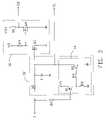
- a delay circuit of an embodiment of the present invention applied in a circuitincludes an input terminal I and two output terminals O 1 , O 2 .
- the input terminal Iis connected to an adjusting circuit 16 via a delay circuit 12 .
- the delay circuit 12includes a resistor R 1 , a capacitor C, and a discharging circuit 14 .
- One terminal of the resistor R 1is connected to the input terminal I, and the other terminal of the resistor R 1 is connected to one terminal of the capacitor C.
- the other terminal of the capacitor Cis connected to ground.
- the discharging circuit 14includes a PNP transistor Q 1 and an NPN transistor Q 2 .
- a base of the PNP transistor Q 1is connected to the input terminal I via a resistor R 6 .
- An emitter of the PNP transistor Q 1is connected to a voltage source V 1 .
- a collector of the PNP transistor Q 1is connected to ground via a resistor R 2 .
- the collector of the PNP transistor Q 1is connected to a base of the NPN transistor Q 2 via a resistor R 3 .
- a collector of the NPN transistor Q 2is connected to the other terminal of the resistor R 1 .
- An emitter of the NPN transistor Q 2is connected to ground.
- the adjusting circuit 16includes two N-channel MOS transistors Q 3 , Q 4 .
- the N-channel MOS transistor Q 3includes a gate connected to the other terminal of the resistor R 1 , a source connected to ground, and a drain connected to a voltage source V 2 via a resistor R 4 .
- the N-channel MOS transistor Q 4includes a gate connected to the drain of the N-channel MOS transistor Q 3 , a source connected to ground, and a drain connected to a voltage source V 3 via a resistor R 5 and to the output O 2 .
- a signal at the input terminal Igoes from low to high level.
- the base of the PNP transistor Q 1which is connected to the input terminal I, is high turning off the PNP transistor Q 1 .
- the capacitor Cwhich is connected to the input terminal I, charges.
- the N-channel MOS transistor Q 3is off and Q 4 is on.
- Signal at the output terminals O 1 , O 2are low.
- the voltage at the output terminal O 1gradually rises with the charging of the capacitor C.
- the voltage at the output terminal O 1is 0.7 (V) turning on the N-channel MOS transistor Q 3 , thus, the gate of the N-channel MOS transistor Q 4 , which is connected to the drain of the N-channel MOS transistor Q 3 , is low turning off the N-channel MOS transistor Q 4 .
- the signal at the output terminal O 2becomes high.
- the signal at the output terminal O 2is delayed by (T 2 b ⁇ T 1 b ) compared to the signal at the input terminal I.
- the input terminal Igoes from high to low level.
- the base of the PNP transistor Q 1connected to the input terminal I, is low turning on the PNP transistor Q 1 .
- the base of the NPN transistor Q 2 connected to the collector of the PNP transistor Q 1is high turning on the NPN transistor Q 2 .
- the capacitoris discharged immediately by the NPN transistor Q 2 .
- the voltage at the output terminal O 1 and the gate of the N-channel MOS transistor Q 3drops immediately, turning off the N-channel MOS transistor Q 3 .
- the gate of N-channel MOS transistor Q 4 connected to the drain of N-channel MOS transistor Q 3is high, turning on the N-channel MOS transistor Q 4 .
- the output terminal O 2is low.
- the output terminal O 2has no delay compared to the input terminal I.
Landscapes
- Physics & Mathematics (AREA)
- Nonlinear Science (AREA)
- Pulse Circuits (AREA)
- Networks Using Active Elements (AREA)
Abstract
Description
Relevant subject matter is disclosed in co-pending U.S. Patent Applications entitled “TIME DELAY CIRCUIT”, assigned to the same assignee with this application.
1. Field of the Invention
The present invention relates to delay circuits, and more particularly to a delay circuit including a resistor and a capacitor.
2. Description of Related Art
Referring toFIG. 2 , at t=T1a, a signal at theinput terminal 10 changes from a low level to a high level. The capacitor C11, which is connected to theinput terminal 10, charges. The voltage at the gate G of the N-channel MOS transistor Q11 gradually rises with the charging of the capacitor C11. A signal at theoutput terminal 11 is high. At t=T2a, the gate voltage of the N-channel MOS transistor Q11 is 2 (V), which turns on the N-channel MOS transistor Q11. At this time, the signal at theoutput terminal 11 become low. The voltage level change of the signal at theoutput terminal 11 is delayed by (T2a−T1a) compared to the voltage level change of the signal atinput terminal 10. At t=T3a, the signal atinput terminal 10 changes from high to low. At this time, the capacitor C11, discharges. The voltage at the gate G of the N-channel MOS transistor Q11 gradually drops with the discharging of the capacitor C11. At t=Ta4, the gate voltage of the N-channel MOS transistor Q11 will be below 2 (V), which will turn off the N-channel MOS transistor Q11. The voltage level change of the signal at theoutput terminal 11 is delayed by (T4a−T3a) compared to the voltage level change of the signal at theinput terminal 10. However, in some circuits, users need to discharge the capacitor immediately.
What is needed, therefore, is a delay circuit which can discharge the capacitor immediately.
A delay circuit comprises a resistor, a capacitor, a PNP transistor, and an NPN transistor. The capacitor has one terminal connected to one terminal of the resistor, and the other terminal connected to ground. The PNP transistor has a base connected to the other terminal of the resistor, a collector, and an emitter connected to a voltage source. The NPN transistor has a base connected to the collector of the PNP transistor, an emitter connected to ground, and a collector connected to the one terminal of the resistor.
Other advantages and novel features of the present invention will become more apparent from the following detailed description of preferred embodiment when taken in conjunction with the accompanying drawings, in which:
Referring toFIG. 3 , a delay circuit of an embodiment of the present invention applied in a circuit includes an input terminal I and two output terminals O1, O2. The input terminal I is connected to an adjustingcircuit 16 via adelay circuit 12.
Thedelay circuit 12 includes a resistor R1, a capacitor C, and adischarging circuit 14. One terminal of the resistor R1 is connected to the input terminal I, and the other terminal of the resistor R1 is connected to one terminal of the capacitor C. The other terminal of the capacitor C is connected to ground.
Thedischarging circuit 14 includes a PNP transistor Q1 and an NPN transistor Q2. A base of the PNP transistor Q1 is connected to the input terminal I via a resistor R6. An emitter of the PNP transistor Q1 is connected to a voltage source V1. A collector of the PNP transistor Q1 is connected to ground via a resistor R2. The collector of the PNP transistor Q1 is connected to a base of the NPN transistor Q2 via a resistor R3. A collector of the NPN transistor Q2 is connected to the other terminal of the resistor R1. An emitter of the NPN transistor Q2 is connected to ground.
The adjustingcircuit 16 includes two N-channel MOS transistors Q3, Q4. The N-channel MOS transistor Q3 includes a gate connected to the other terminal of the resistor R1, a source connected to ground, and a drain connected to a voltage source V2 via a resistor R4. The N-channel MOS transistor Q4 includes a gate connected to the drain of the N-channel MOS transistor Q3, a source connected to ground, and a drain connected to a voltage source V3 via a resistor R5 and to the output O2.
Referring also toFIGS. 3 and 4 , at t=T1b, a signal at the input terminal I goes from low to high level. The base of the PNP transistor Q1, which is connected to the input terminal I, is high turning off the PNP transistor Q1. The capacitor C, which is connected to the input terminal I, charges. The N-channel MOS transistor Q3 is off and Q4 is on. Signal at the output terminals O1, O2 are low. The voltage at the output terminal O1 gradually rises with the charging of the capacitor C. At t=T2b,the voltage at the output terminal O1 is 0.7 (V) turning on the N-channel MOS transistor Q3, thus, the gate of the N-channel MOS transistor Q4, which is connected to the drain of the N-channel MOS transistor Q3, is low turning off the N-channel MOS transistor Q4. The signal at the output terminal O2 becomes high. The signal at the output terminal O2 is delayed by (T2b−T1b) compared to the signal at the input terminal I. At t=T3b,the input terminal I goes from high to low level. The base of the PNP transistor Q1, connected to the input terminal I, is low turning on the PNP transistor Q1. The base of the NPN transistor Q2 connected to the collector of the PNP transistor Q1 is high turning on the NPN transistor Q2. The capacitor is discharged immediately by the NPN transistor Q2. The voltage at the output terminal O1 and the gate of the N-channel MOS transistor Q3 drops immediately, turning off the N-channel MOS transistor Q3. At this time, the gate of N-channel MOS transistor Q4 connected to the drain of N-channel MOS transistor Q3 is high, turning on the N-channel MOS transistor Q4. The output terminal O2 is low. The output terminal O2 has no delay compared to the input terminal I.
It is to be understood, however, that even though numerous characteristics and advantages of the present invention have been set forth in the foregoing description, together with details of the structure and function of the invention, the disclosure is illustrative only, and changes may be made in detail, especially in matters of shape, size, and arrangement of parts within the principles of the invention to the full extent indicated by the broad general meaning of the terms in which the appended claims are expressed.
Claims (3)
1. A delay circuit, comprising:
an RC circuit comprising a resistor having one end configured for receiving an input signal and an opposite end, and a capacitor connected to the opposite end of the resistor
a discharging circuit connected to the RC circuit for controllable discharging of the capacitor, the discharging circuit comprising a controllable current path connected between the capacitor and ground, and a control terminal connected to the one end of the resistor configured for sensing a status of the RC circuit to control conduction of the path, the discharging circuit comprises a PNP type transistor and an NPN type transistor, a base of the PNP type transistor acts as the control terminal, an emitter of the PNP transistor is connected to a high level voltage signal, a collector of the PNP type transitor is connected to ground via a resistor, a base of NPN type transistor is connected to the collector of the PNP type transistor, a collector of the NPN type transistor is connected to the capacitor, and an emitter of the NPN type transistor is connected to ground;
wherein when the control terminal senses the RC circuit starts charging, the control terminal closes the path such that the capacitor charges gradually, and when the control terminal senses the RC circuit starts discharging, the control terminal opens the path to quickly discharge the capacitor.
2. A sequence circuit, comprising:
a resistor, one terminal of the resistor connected to an input terminal, the other terminal of the resistor connected to a first output terminal;
a capacitor having one terminal connected to the other terminal of the resistor, and the other terminal connected to ground;
a discharging circuit having a terminal connected to the one terminal of the resistor, another terminal connected to the other terminal of the resistor, the discharging circuit comprising a PNP transistor and a NPN transistor, the PNP transistor having a base connected to the one terminal of the resistor, a collector, and an emitter connected to a voltage source, the NPN transistor having a base connected to the collector of the PNP transistor, an emitter connected to ground, and a collector connected to the other terminal of the resistor; and
an adjusting circuit with a terminal connected to the other terminal of the resistor, and another terminal connected to a second output terminal,
wherein when a sequence signal applied at the input terminal goes from low to high level, the voltage at the first output terminal gradually rises with charging of the capacitor and the change of the voltage level of the signal at the second output terminal is delayed a predetermined time compared to the change of the voltage level of the signal at the input terminal; when the signal at the input terminal goes from high to low level, the capacitor discharges via the discharging circuit in such a manner that the voltage at the first output terminal drops immediately and, the change of the voltage level of the signal at the second output terminal is substantially synchronous with the signal at the input terminal.
3. The sequence circuit as described inclaim 2 , wherein the adjusting circuit comprises a first N-channel MOS transistor and a second N-channel MOS transistor, the first N-channel MOS transistor having a gate connected to the other terminal of the resistor, a source connected to ground, and a drain connected to first voltage source via a resistor, the second N-channel MOS transistor having a gate connected to the drain of the first N-channel MOS transistor, a source connected to ground, and a drain connected to a second voltage source via a resistor and to the second output terminal.
Applications Claiming Priority (2)
| Application Number | Priority Date | Filing Date | Title |
|---|---|---|---|
| CNU2007202001273UCN201025702Y (en) | 2007-03-08 | 2007-03-08 | delay circuit |
| CN200720200127.3 | 2007-03-08 |
Publications (2)
| Publication Number | Publication Date |
|---|---|
| US20080218236A1 US20080218236A1 (en) | 2008-09-11 |
| US7518429B2true US7518429B2 (en) | 2009-04-14 |
Family
ID=39099558
Family Applications (1)
| Application Number | Title | Priority Date | Filing Date |
|---|---|---|---|
| US11/767,478Expired - Fee RelatedUS7518429B2 (en) | 2007-03-08 | 2007-06-23 | Delay circuit |
Country Status (2)
| Country | Link |
|---|---|
| US (1) | US7518429B2 (en) |
| CN (1) | CN201025702Y (en) |
Cited By (1)
| Publication number | Priority date | Publication date | Assignee | Title |
|---|---|---|---|---|
| US20080150604A1 (en)* | 2006-12-22 | 2008-06-26 | Norbert Huber | Converter having a time-delay circuit for pwm signals |
Families Citing this family (4)
| Publication number | Priority date | Publication date | Assignee | Title |
|---|---|---|---|---|
| CN102457256A (en)* | 2010-10-20 | 2012-05-16 | 鸿富锦精密工业(深圳)有限公司 | Reset signal delay circuit |
| CN105703763B (en)* | 2010-12-08 | 2019-02-22 | 深圳迈辽技术转移中心有限公司 | Voltage sequence output circuit |
| CN105703762B (en)* | 2010-12-08 | 2019-03-26 | 南京瑞贻电子科技有限公司 | Voltage sequence output circuit |
| KR102505431B1 (en)* | 2018-06-22 | 2023-03-03 | 삼성전기주식회사 | Voltage control circuit |
Citations (3)
| Publication number | Priority date | Publication date | Assignee | Title |
|---|---|---|---|---|
| US4430587A (en)* | 1982-01-13 | 1984-02-07 | Rockwell International Corporation | MOS Fixed delay circuit |
| US4746823A (en)* | 1986-07-02 | 1988-05-24 | Dallas Semiconductor Corporation | Voltage-insensitive and temperature-compensated delay circuit for a monolithic integrated circuit |
| US6940333B2 (en)* | 2003-07-14 | 2005-09-06 | Realtek Semiconductor Corp. | High-to-low level shifter |
- 2007
- 2007-03-08CNCNU2007202001273Upatent/CN201025702Y/ennot_activeExpired - Fee Related
- 2007-06-23USUS11/767,478patent/US7518429B2/ennot_activeExpired - Fee Related
Patent Citations (3)
| Publication number | Priority date | Publication date | Assignee | Title |
|---|---|---|---|---|
| US4430587A (en)* | 1982-01-13 | 1984-02-07 | Rockwell International Corporation | MOS Fixed delay circuit |
| US4746823A (en)* | 1986-07-02 | 1988-05-24 | Dallas Semiconductor Corporation | Voltage-insensitive and temperature-compensated delay circuit for a monolithic integrated circuit |
| US6940333B2 (en)* | 2003-07-14 | 2005-09-06 | Realtek Semiconductor Corp. | High-to-low level shifter |
Cited By (2)
| Publication number | Priority date | Publication date | Assignee | Title |
|---|---|---|---|---|
| US20080150604A1 (en)* | 2006-12-22 | 2008-06-26 | Norbert Huber | Converter having a time-delay circuit for pwm signals |
| US7586352B2 (en)* | 2006-12-22 | 2009-09-08 | Dr. Johannes Heidenhain Gmbh | Converter having a time-delay circuit for PWM signals |
Also Published As
| Publication number | Publication date |
|---|---|
| US20080218236A1 (en) | 2008-09-11 |
| CN201025702Y (en) | 2008-02-20 |
Similar Documents
| Publication | Publication Date | Title |
|---|---|---|
| US8063675B2 (en) | Delay circuit including first and second internal delay circuits and a selection switch | |
| US8004337B2 (en) | Digital delay circuit | |
| US20060220727A1 (en) | Electronic switch and operational method for transistor | |
| US7659767B2 (en) | Boost circuit and level shifter | |
| US20080157844A1 (en) | Time delay circuit | |
| JPH07154221A (en) | Delay circuit | |
| US7518429B2 (en) | Delay circuit | |
| US20030151448A1 (en) | Negative voltage output charge pump circuit | |
| US6677798B2 (en) | High speed voltage level shifter | |
| US20070008026A1 (en) | Clamping circuit | |
| US8896277B2 (en) | Voltage regulator | |
| US20080084232A1 (en) | Negative voltage detector | |
| US7268623B2 (en) | Low voltage differential signal driver circuit and method for controlling the same | |
| US20090243669A1 (en) | Power-on reset circuit | |
| US8013658B2 (en) | Circuit for controlling time sequence | |
| US7276961B2 (en) | Constant voltage outputting circuit | |
| US7268604B2 (en) | Comparator with hysteresis and method of comparing using the same | |
| US7164300B2 (en) | Power-low reset circuit | |
| US5929686A (en) | Semiconductor device with boot-strap output circuit and clamping circuit | |
| US6924694B2 (en) | Switch circuit | |
| US20070103210A1 (en) | Power-on reset circuit for an integrated circuit | |
| US20230231551A1 (en) | High bandwidth and low power transmitter | |
| US20090160506A1 (en) | Power-on clear circuit | |
| US8129965B2 (en) | Quick-start low dropout regulator | |
| US8872555B2 (en) | Power-on reset circuit |
Legal Events
| Date | Code | Title | Description |
|---|---|---|---|
| AS | Assignment | Owner name:HON HAI PRECISION INDUSTRY CO., LTD., TAIWAN Free format text:ASSIGNMENT OF ASSIGNORS INTEREST;ASSIGNORS:LIU, BAI-HONG;REN, ZE-SHU;REEL/FRAME:019471/0030 Effective date:20070615 | |
| AS | Assignment | Owner name:HON HAI PRECISION INDUSTRY CO., LTD., TAIWAN Free format text:ASSIGNMENT OF ASSIGNORS INTEREST;ASSIGNOR:HON HAI PRECISION INDUSTRY CO., LTD.;REEL/FRAME:022051/0206 Effective date:20081230 Owner name:HONG FU JIN PRECISION INDUSTRY (SHENZHEN) CO., LTD Free format text:ASSIGNMENT OF ASSIGNORS INTEREST;ASSIGNOR:HON HAI PRECISION INDUSTRY CO., LTD.;REEL/FRAME:022051/0206 Effective date:20081230 | |
| FPAY | Fee payment | Year of fee payment:4 | |
| REMI | Maintenance fee reminder mailed | ||
| LAPS | Lapse for failure to pay maintenance fees | ||
| STCH | Information on status: patent discontinuation | Free format text:PATENT EXPIRED DUE TO NONPAYMENT OF MAINTENANCE FEES UNDER 37 CFR 1.362 | |
| FP | Lapsed due to failure to pay maintenance fee | Effective date:20170414 |