US7518223B2 - Semiconductor devices and semiconductor device assemblies including a nonconfluent spacer layer - Google Patents
Semiconductor devices and semiconductor device assemblies including a nonconfluent spacer layerDownload PDFInfo
- Publication number
- US7518223B2 US7518223B2US09/939,253US93925301AUS7518223B2US 7518223 B2US7518223 B2US 7518223B2US 93925301 AUS93925301 AUS 93925301AUS 7518223 B2US7518223 B2US 7518223B2
- Authority
- US
- United States
- Prior art keywords
- semiconductor device
- spacer layer
- nonconfluent
- semiconductor
- device assembly
- Prior art date
- Legal status (The legal status is an assumption and is not a legal conclusion. Google has not performed a legal analysis and makes no representation as to the accuracy of the status listed.)
- Expired - Lifetime, expires
Links
Images


Classifications
- H—ELECTRICITY
- H01—ELECTRIC ELEMENTS
- H01L—SEMICONDUCTOR DEVICES NOT COVERED BY CLASS H10
- H01L23/00—Details of semiconductor or other solid state devices
- H01L23/28—Encapsulations, e.g. encapsulating layers, coatings, e.g. for protection
- H01L23/31—Encapsulations, e.g. encapsulating layers, coatings, e.g. for protection characterised by the arrangement or shape
- H01L23/3107—Encapsulations, e.g. encapsulating layers, coatings, e.g. for protection characterised by the arrangement or shape the device being completely enclosed
- H01L23/3121—Encapsulations, e.g. encapsulating layers, coatings, e.g. for protection characterised by the arrangement or shape the device being completely enclosed a substrate forming part of the encapsulation
- H01L23/3128—Encapsulations, e.g. encapsulating layers, coatings, e.g. for protection characterised by the arrangement or shape the device being completely enclosed a substrate forming part of the encapsulation the substrate having spherical bumps for external connection
- H—ELECTRICITY
- H01—ELECTRIC ELEMENTS
- H01L—SEMICONDUCTOR DEVICES NOT COVERED BY CLASS H10
- H01L23/00—Details of semiconductor or other solid state devices
- H01L23/48—Arrangements for conducting electric current to or from the solid state body in operation, e.g. leads, terminal arrangements ; Selection of materials therefor
- H01L23/488—Arrangements for conducting electric current to or from the solid state body in operation, e.g. leads, terminal arrangements ; Selection of materials therefor consisting of soldered or bonded constructions
- H01L23/495—Lead-frames or other flat leads
- H01L23/49575—Assemblies of semiconductor devices on lead frames
- H—ELECTRICITY
- H01—ELECTRIC ELEMENTS
- H01L—SEMICONDUCTOR DEVICES NOT COVERED BY CLASS H10
- H01L25/00—Assemblies consisting of a plurality of semiconductor or other solid state devices
- H01L25/03—Assemblies consisting of a plurality of semiconductor or other solid state devices all the devices being of a type provided for in a single subclass of subclasses H10B, H10D, H10F, H10H, H10K or H10N, e.g. assemblies of rectifier diodes
- H01L25/04—Assemblies consisting of a plurality of semiconductor or other solid state devices all the devices being of a type provided for in a single subclass of subclasses H10B, H10D, H10F, H10H, H10K or H10N, e.g. assemblies of rectifier diodes the devices not having separate containers
- H01L25/065—Assemblies consisting of a plurality of semiconductor or other solid state devices all the devices being of a type provided for in a single subclass of subclasses H10B, H10D, H10F, H10H, H10K or H10N, e.g. assemblies of rectifier diodes the devices not having separate containers the devices being of a type provided for in group H10D89/00
- H01L25/0657—Stacked arrangements of devices
- H—ELECTRICITY
- H01—ELECTRIC ELEMENTS
- H01L—SEMICONDUCTOR DEVICES NOT COVERED BY CLASS H10
- H01L25/00—Assemblies consisting of a plurality of semiconductor or other solid state devices
- H01L25/50—Multistep manufacturing processes of assemblies consisting of devices, the devices being individual devices of subclass H10D or integrated devices of class H10
- B—PERFORMING OPERATIONS; TRANSPORTING
- B33—ADDITIVE MANUFACTURING TECHNOLOGY
- B33Y—ADDITIVE MANUFACTURING, i.e. MANUFACTURING OF THREE-DIMENSIONAL [3-D] OBJECTS BY ADDITIVE DEPOSITION, ADDITIVE AGGLOMERATION OR ADDITIVE LAYERING, e.g. BY 3-D PRINTING, STEREOLITHOGRAPHY OR SELECTIVE LASER SINTERING
- B33Y80/00—Products made by additive manufacturing
- H—ELECTRICITY
- H01—ELECTRIC ELEMENTS
- H01L—SEMICONDUCTOR DEVICES NOT COVERED BY CLASS H10
- H01L2224/00—Indexing scheme for arrangements for connecting or disconnecting semiconductor or solid-state bodies and methods related thereto as covered by H01L24/00
- H01L2224/01—Means for bonding being attached to, or being formed on, the surface to be connected, e.g. chip-to-package, die-attach, "first-level" interconnects; Manufacturing methods related thereto
- H01L2224/02—Bonding areas; Manufacturing methods related thereto
- H01L2224/04—Structure, shape, material or disposition of the bonding areas prior to the connecting process
- H01L2224/05—Structure, shape, material or disposition of the bonding areas prior to the connecting process of an individual bonding area
- H01L2224/0554—External layer
- H01L2224/05599—Material
- H—ELECTRICITY
- H01—ELECTRIC ELEMENTS
- H01L—SEMICONDUCTOR DEVICES NOT COVERED BY CLASS H10
- H01L2224/00—Indexing scheme for arrangements for connecting or disconnecting semiconductor or solid-state bodies and methods related thereto as covered by H01L24/00
- H01L2224/01—Means for bonding being attached to, or being formed on, the surface to be connected, e.g. chip-to-package, die-attach, "first-level" interconnects; Manufacturing methods related thereto
- H01L2224/26—Layer connectors, e.g. plate connectors, solder or adhesive layers; Manufacturing methods related thereto
- H01L2224/31—Structure, shape, material or disposition of the layer connectors after the connecting process
- H01L2224/32—Structure, shape, material or disposition of the layer connectors after the connecting process of an individual layer connector
- H01L2224/321—Disposition
- H01L2224/32135—Disposition the layer connector connecting between different semiconductor or solid-state bodies, i.e. chip-to-chip
- H01L2224/32145—Disposition the layer connector connecting between different semiconductor or solid-state bodies, i.e. chip-to-chip the bodies being stacked
- H—ELECTRICITY
- H01—ELECTRIC ELEMENTS
- H01L—SEMICONDUCTOR DEVICES NOT COVERED BY CLASS H10
- H01L2224/00—Indexing scheme for arrangements for connecting or disconnecting semiconductor or solid-state bodies and methods related thereto as covered by H01L24/00
- H01L2224/01—Means for bonding being attached to, or being formed on, the surface to be connected, e.g. chip-to-package, die-attach, "first-level" interconnects; Manufacturing methods related thereto
- H01L2224/26—Layer connectors, e.g. plate connectors, solder or adhesive layers; Manufacturing methods related thereto
- H01L2224/31—Structure, shape, material or disposition of the layer connectors after the connecting process
- H01L2224/32—Structure, shape, material or disposition of the layer connectors after the connecting process of an individual layer connector
- H01L2224/321—Disposition
- H01L2224/32151—Disposition the layer connector connecting between a semiconductor or solid-state body and an item not being a semiconductor or solid-state body, e.g. chip-to-substrate, chip-to-passive
- H01L2224/32221—Disposition the layer connector connecting between a semiconductor or solid-state body and an item not being a semiconductor or solid-state body, e.g. chip-to-substrate, chip-to-passive the body and the item being stacked
- H01L2224/32225—Disposition the layer connector connecting between a semiconductor or solid-state body and an item not being a semiconductor or solid-state body, e.g. chip-to-substrate, chip-to-passive the body and the item being stacked the item being non-metallic, e.g. insulating substrate with or without metallisation
- H—ELECTRICITY
- H01—ELECTRIC ELEMENTS
- H01L—SEMICONDUCTOR DEVICES NOT COVERED BY CLASS H10
- H01L2224/00—Indexing scheme for arrangements for connecting or disconnecting semiconductor or solid-state bodies and methods related thereto as covered by H01L24/00
- H01L2224/01—Means for bonding being attached to, or being formed on, the surface to be connected, e.g. chip-to-package, die-attach, "first-level" interconnects; Manufacturing methods related thereto
- H01L2224/42—Wire connectors; Manufacturing methods related thereto
- H01L2224/47—Structure, shape, material or disposition of the wire connectors after the connecting process
- H01L2224/48—Structure, shape, material or disposition of the wire connectors after the connecting process of an individual wire connector
- H01L2224/4805—Shape
- H01L2224/4809—Loop shape
- H01L2224/48091—Arched
- H—ELECTRICITY
- H01—ELECTRIC ELEMENTS
- H01L—SEMICONDUCTOR DEVICES NOT COVERED BY CLASS H10
- H01L2224/00—Indexing scheme for arrangements for connecting or disconnecting semiconductor or solid-state bodies and methods related thereto as covered by H01L24/00
- H01L2224/01—Means for bonding being attached to, or being formed on, the surface to be connected, e.g. chip-to-package, die-attach, "first-level" interconnects; Manufacturing methods related thereto
- H01L2224/42—Wire connectors; Manufacturing methods related thereto
- H01L2224/47—Structure, shape, material or disposition of the wire connectors after the connecting process
- H01L2224/48—Structure, shape, material or disposition of the wire connectors after the connecting process of an individual wire connector
- H01L2224/481—Disposition
- H01L2224/48151—Connecting between a semiconductor or solid-state body and an item not being a semiconductor or solid-state body, e.g. chip-to-substrate, chip-to-passive
- H01L2224/48221—Connecting between a semiconductor or solid-state body and an item not being a semiconductor or solid-state body, e.g. chip-to-substrate, chip-to-passive the body and the item being stacked
- H01L2224/48225—Connecting between a semiconductor or solid-state body and an item not being a semiconductor or solid-state body, e.g. chip-to-substrate, chip-to-passive the body and the item being stacked the item being non-metallic, e.g. insulating substrate with or without metallisation
- H01L2224/48227—Connecting between a semiconductor or solid-state body and an item not being a semiconductor or solid-state body, e.g. chip-to-substrate, chip-to-passive the body and the item being stacked the item being non-metallic, e.g. insulating substrate with or without metallisation connecting the wire to a bond pad of the item
- H—ELECTRICITY
- H01—ELECTRIC ELEMENTS
- H01L—SEMICONDUCTOR DEVICES NOT COVERED BY CLASS H10
- H01L2224/00—Indexing scheme for arrangements for connecting or disconnecting semiconductor or solid-state bodies and methods related thereto as covered by H01L24/00
- H01L2224/01—Means for bonding being attached to, or being formed on, the surface to be connected, e.g. chip-to-package, die-attach, "first-level" interconnects; Manufacturing methods related thereto
- H01L2224/42—Wire connectors; Manufacturing methods related thereto
- H01L2224/47—Structure, shape, material or disposition of the wire connectors after the connecting process
- H01L2224/48—Structure, shape, material or disposition of the wire connectors after the connecting process of an individual wire connector
- H01L2224/481—Disposition
- H01L2224/48151—Connecting between a semiconductor or solid-state body and an item not being a semiconductor or solid-state body, e.g. chip-to-substrate, chip-to-passive
- H01L2224/48221—Connecting between a semiconductor or solid-state body and an item not being a semiconductor or solid-state body, e.g. chip-to-substrate, chip-to-passive the body and the item being stacked
- H01L2224/48245—Connecting between a semiconductor or solid-state body and an item not being a semiconductor or solid-state body, e.g. chip-to-substrate, chip-to-passive the body and the item being stacked the item being metallic
- H01L2224/48247—Connecting between a semiconductor or solid-state body and an item not being a semiconductor or solid-state body, e.g. chip-to-substrate, chip-to-passive the body and the item being stacked the item being metallic connecting the wire to a bond pad of the item
- H—ELECTRICITY
- H01—ELECTRIC ELEMENTS
- H01L—SEMICONDUCTOR DEVICES NOT COVERED BY CLASS H10
- H01L2224/00—Indexing scheme for arrangements for connecting or disconnecting semiconductor or solid-state bodies and methods related thereto as covered by H01L24/00
- H01L2224/01—Means for bonding being attached to, or being formed on, the surface to be connected, e.g. chip-to-package, die-attach, "first-level" interconnects; Manufacturing methods related thereto
- H01L2224/42—Wire connectors; Manufacturing methods related thereto
- H01L2224/47—Structure, shape, material or disposition of the wire connectors after the connecting process
- H01L2224/48—Structure, shape, material or disposition of the wire connectors after the connecting process of an individual wire connector
- H01L2224/4899—Auxiliary members for wire connectors, e.g. flow-barriers, reinforcing structures, spacers, alignment aids
- H01L2224/48991—Auxiliary members for wire connectors, e.g. flow-barriers, reinforcing structures, spacers, alignment aids being formed on the semiconductor or solid-state body to be connected
- H01L2224/48992—Reinforcing structures
- H—ELECTRICITY
- H01—ELECTRIC ELEMENTS
- H01L—SEMICONDUCTOR DEVICES NOT COVERED BY CLASS H10
- H01L2224/00—Indexing scheme for arrangements for connecting or disconnecting semiconductor or solid-state bodies and methods related thereto as covered by H01L24/00
- H01L2224/01—Means for bonding being attached to, or being formed on, the surface to be connected, e.g. chip-to-package, die-attach, "first-level" interconnects; Manufacturing methods related thereto
- H01L2224/42—Wire connectors; Manufacturing methods related thereto
- H01L2224/47—Structure, shape, material or disposition of the wire connectors after the connecting process
- H01L2224/49—Structure, shape, material or disposition of the wire connectors after the connecting process of a plurality of wire connectors
- H01L2224/491—Disposition
- H01L2224/4912—Layout
- H01L2224/49171—Fan-out arrangements
- H—ELECTRICITY
- H01—ELECTRIC ELEMENTS
- H01L—SEMICONDUCTOR DEVICES NOT COVERED BY CLASS H10
- H01L2224/00—Indexing scheme for arrangements for connecting or disconnecting semiconductor or solid-state bodies and methods related thereto as covered by H01L24/00
- H01L2224/73—Means for bonding being of different types provided for in two or more of groups H01L2224/10, H01L2224/18, H01L2224/26, H01L2224/34, H01L2224/42, H01L2224/50, H01L2224/63, H01L2224/71
- H01L2224/732—Location after the connecting process
- H01L2224/73251—Location after the connecting process on different surfaces
- H01L2224/73265—Layer and wire connectors
- H—ELECTRICITY
- H01—ELECTRIC ELEMENTS
- H01L—SEMICONDUCTOR DEVICES NOT COVERED BY CLASS H10
- H01L2224/00—Indexing scheme for arrangements for connecting or disconnecting semiconductor or solid-state bodies and methods related thereto as covered by H01L24/00
- H01L2224/80—Methods for connecting semiconductor or other solid state bodies using means for bonding being attached to, or being formed on, the surface to be connected
- H01L2224/83—Methods for connecting semiconductor or other solid state bodies using means for bonding being attached to, or being formed on, the surface to be connected using a layer connector
- H01L2224/8312—Aligning
- H01L2224/83136—Aligning involving guiding structures, e.g. spacers or supporting members
- H01L2224/83138—Aligning involving guiding structures, e.g. spacers or supporting members the guiding structures being at least partially left in the finished device
- H01L2224/83139—Guiding structures on the body
- H—ELECTRICITY
- H01—ELECTRIC ELEMENTS
- H01L—SEMICONDUCTOR DEVICES NOT COVERED BY CLASS H10
- H01L2224/00—Indexing scheme for arrangements for connecting or disconnecting semiconductor or solid-state bodies and methods related thereto as covered by H01L24/00
- H01L2224/80—Methods for connecting semiconductor or other solid state bodies using means for bonding being attached to, or being formed on, the surface to be connected
- H01L2224/85—Methods for connecting semiconductor or other solid state bodies using means for bonding being attached to, or being formed on, the surface to be connected using a wire connector
- H01L2224/8538—Bonding interfaces outside the semiconductor or solid-state body
- H01L2224/85399—Material
- H—ELECTRICITY
- H01—ELECTRIC ELEMENTS
- H01L—SEMICONDUCTOR DEVICES NOT COVERED BY CLASS H10
- H01L2224/00—Indexing scheme for arrangements for connecting or disconnecting semiconductor or solid-state bodies and methods related thereto as covered by H01L24/00
- H01L2224/80—Methods for connecting semiconductor or other solid state bodies using means for bonding being attached to, or being formed on, the surface to be connected
- H01L2224/85—Methods for connecting semiconductor or other solid state bodies using means for bonding being attached to, or being formed on, the surface to be connected using a wire connector
- H01L2224/85909—Post-treatment of the connector or wire bonding area
- H01L2224/8592—Applying permanent coating, e.g. protective coating
- H—ELECTRICITY
- H01—ELECTRIC ELEMENTS
- H01L—SEMICONDUCTOR DEVICES NOT COVERED BY CLASS H10
- H01L2225/00—Details relating to assemblies covered by the group H01L25/00 but not provided for in its subgroups
- H01L2225/03—All the devices being of a type provided for in the same main group of the same subclass of class H10, e.g. assemblies of rectifier diodes
- H01L2225/04—All the devices being of a type provided for in the same main group of the same subclass of class H10, e.g. assemblies of rectifier diodes the devices not having separate containers
- H01L2225/065—All the devices being of a type provided for in the same main group of the same subclass of class H10
- H01L2225/06503—Stacked arrangements of devices
- H01L2225/0651—Wire or wire-like electrical connections from device to substrate
- H—ELECTRICITY
- H01—ELECTRIC ELEMENTS
- H01L—SEMICONDUCTOR DEVICES NOT COVERED BY CLASS H10
- H01L2225/00—Details relating to assemblies covered by the group H01L25/00 but not provided for in its subgroups
- H01L2225/03—All the devices being of a type provided for in the same main group of the same subclass of class H10, e.g. assemblies of rectifier diodes
- H01L2225/04—All the devices being of a type provided for in the same main group of the same subclass of class H10, e.g. assemblies of rectifier diodes the devices not having separate containers
- H01L2225/065—All the devices being of a type provided for in the same main group of the same subclass of class H10
- H01L2225/06503—Stacked arrangements of devices
- H01L2225/06513—Bump or bump-like direct electrical connections between devices, e.g. flip-chip connection, solder bumps
- H—ELECTRICITY
- H01—ELECTRIC ELEMENTS
- H01L—SEMICONDUCTOR DEVICES NOT COVERED BY CLASS H10
- H01L2225/00—Details relating to assemblies covered by the group H01L25/00 but not provided for in its subgroups
- H01L2225/03—All the devices being of a type provided for in the same main group of the same subclass of class H10, e.g. assemblies of rectifier diodes
- H01L2225/04—All the devices being of a type provided for in the same main group of the same subclass of class H10, e.g. assemblies of rectifier diodes the devices not having separate containers
- H01L2225/065—All the devices being of a type provided for in the same main group of the same subclass of class H10
- H01L2225/06503—Stacked arrangements of devices
- H01L2225/06575—Auxiliary carrier between devices, the carrier having no electrical connection structure
- H—ELECTRICITY
- H01—ELECTRIC ELEMENTS
- H01L—SEMICONDUCTOR DEVICES NOT COVERED BY CLASS H10
- H01L2225/00—Details relating to assemblies covered by the group H01L25/00 but not provided for in its subgroups
- H01L2225/03—All the devices being of a type provided for in the same main group of the same subclass of class H10, e.g. assemblies of rectifier diodes
- H01L2225/04—All the devices being of a type provided for in the same main group of the same subclass of class H10, e.g. assemblies of rectifier diodes the devices not having separate containers
- H01L2225/065—All the devices being of a type provided for in the same main group of the same subclass of class H10
- H01L2225/06503—Stacked arrangements of devices
- H01L2225/06582—Housing for the assembly, e.g. chip scale package [CSP]
- H01L2225/06586—Housing with external bump or bump-like connectors
- H—ELECTRICITY
- H01—ELECTRIC ELEMENTS
- H01L—SEMICONDUCTOR DEVICES NOT COVERED BY CLASS H10
- H01L24/00—Arrangements for connecting or disconnecting semiconductor or solid-state bodies; Methods or apparatus related thereto
- H01L24/01—Means for bonding being attached to, or being formed on, the surface to be connected, e.g. chip-to-package, die-attach, "first-level" interconnects; Manufacturing methods related thereto
- H01L24/42—Wire connectors; Manufacturing methods related thereto
- H01L24/47—Structure, shape, material or disposition of the wire connectors after the connecting process
- H01L24/48—Structure, shape, material or disposition of the wire connectors after the connecting process of an individual wire connector
- H—ELECTRICITY
- H01—ELECTRIC ELEMENTS
- H01L—SEMICONDUCTOR DEVICES NOT COVERED BY CLASS H10
- H01L24/00—Arrangements for connecting or disconnecting semiconductor or solid-state bodies; Methods or apparatus related thereto
- H01L24/01—Means for bonding being attached to, or being formed on, the surface to be connected, e.g. chip-to-package, die-attach, "first-level" interconnects; Manufacturing methods related thereto
- H01L24/42—Wire connectors; Manufacturing methods related thereto
- H01L24/47—Structure, shape, material or disposition of the wire connectors after the connecting process
- H01L24/49—Structure, shape, material or disposition of the wire connectors after the connecting process of a plurality of wire connectors
- H—ELECTRICITY
- H01—ELECTRIC ELEMENTS
- H01L—SEMICONDUCTOR DEVICES NOT COVERED BY CLASS H10
- H01L24/00—Arrangements for connecting or disconnecting semiconductor or solid-state bodies; Methods or apparatus related thereto
- H01L24/73—Means for bonding being of different types provided for in two or more of groups H01L24/10, H01L24/18, H01L24/26, H01L24/34, H01L24/42, H01L24/50, H01L24/63, H01L24/71
- H—ELECTRICITY
- H01—ELECTRIC ELEMENTS
- H01L—SEMICONDUCTOR DEVICES NOT COVERED BY CLASS H10
- H01L2924/00—Indexing scheme for arrangements or methods for connecting or disconnecting semiconductor or solid-state bodies as covered by H01L24/00
- H01L2924/0001—Technical content checked by a classifier
- H01L2924/00014—Technical content checked by a classifier the subject-matter covered by the group, the symbol of which is combined with the symbol of this group, being disclosed without further technical details
- H—ELECTRICITY
- H01—ELECTRIC ELEMENTS
- H01L—SEMICONDUCTOR DEVICES NOT COVERED BY CLASS H10
- H01L2924/00—Indexing scheme for arrangements or methods for connecting or disconnecting semiconductor or solid-state bodies as covered by H01L24/00
- H01L2924/01—Chemical elements
- H01L2924/01006—Carbon [C]
- H—ELECTRICITY
- H01—ELECTRIC ELEMENTS
- H01L—SEMICONDUCTOR DEVICES NOT COVERED BY CLASS H10
- H01L2924/00—Indexing scheme for arrangements or methods for connecting or disconnecting semiconductor or solid-state bodies as covered by H01L24/00
- H01L2924/01—Chemical elements
- H01L2924/01013—Aluminum [Al]
- H—ELECTRICITY
- H01—ELECTRIC ELEMENTS
- H01L—SEMICONDUCTOR DEVICES NOT COVERED BY CLASS H10
- H01L2924/00—Indexing scheme for arrangements or methods for connecting or disconnecting semiconductor or solid-state bodies as covered by H01L24/00
- H01L2924/01—Chemical elements
- H01L2924/01014—Silicon [Si]
- H—ELECTRICITY
- H01—ELECTRIC ELEMENTS
- H01L—SEMICONDUCTOR DEVICES NOT COVERED BY CLASS H10
- H01L2924/00—Indexing scheme for arrangements or methods for connecting or disconnecting semiconductor or solid-state bodies as covered by H01L24/00
- H01L2924/01—Chemical elements
- H01L2924/01075—Rhenium [Re]
- H—ELECTRICITY
- H01—ELECTRIC ELEMENTS
- H01L—SEMICONDUCTOR DEVICES NOT COVERED BY CLASS H10
- H01L2924/00—Indexing scheme for arrangements or methods for connecting or disconnecting semiconductor or solid-state bodies as covered by H01L24/00
- H01L2924/013—Alloys
- H01L2924/014—Solder alloys
- H—ELECTRICITY
- H01—ELECTRIC ELEMENTS
- H01L—SEMICONDUCTOR DEVICES NOT COVERED BY CLASS H10
- H01L2924/00—Indexing scheme for arrangements or methods for connecting or disconnecting semiconductor or solid-state bodies as covered by H01L24/00
- H01L2924/10—Details of semiconductor or other solid state devices to be connected
- H01L2924/11—Device type
- H01L2924/12—Passive devices, e.g. 2 terminal devices
- H01L2924/1204—Optical Diode
- H01L2924/12042—LASER
- H—ELECTRICITY
- H01—ELECTRIC ELEMENTS
- H01L—SEMICONDUCTOR DEVICES NOT COVERED BY CLASS H10
- H01L2924/00—Indexing scheme for arrangements or methods for connecting or disconnecting semiconductor or solid-state bodies as covered by H01L24/00
- H01L2924/15—Details of package parts other than the semiconductor or other solid state devices to be connected
- H01L2924/151—Die mounting substrate
- H01L2924/153—Connection portion
- H01L2924/1531—Connection portion the connection portion being formed only on the surface of the substrate opposite to the die mounting surface
- H01L2924/15311—Connection portion the connection portion being formed only on the surface of the substrate opposite to the die mounting surface being a ball array, e.g. BGA
- H—ELECTRICITY
- H01—ELECTRIC ELEMENTS
- H01L—SEMICONDUCTOR DEVICES NOT COVERED BY CLASS H10
- H01L2924/00—Indexing scheme for arrangements or methods for connecting or disconnecting semiconductor or solid-state bodies as covered by H01L24/00
- H01L2924/15—Details of package parts other than the semiconductor or other solid state devices to be connected
- H01L2924/181—Encapsulation
Definitions
- the present inventionrelates generally to multi-chip modules and, more specifically, to multi-chip modules that include semiconductor devices in stacked arrangement.
- the present inventionrelates to multi-chip modules that include at least one semiconductor device with a spacer predisposed on a surface thereof and another semiconductor device in stacked relation thereto and spaced vertically apart therefrom by way of the predisposed spacer. More particularly, the predisposed spacer may be printed onto a surface of the at least one semiconductor device.
- multi-chip moduleIn order to conserve the amount of surface area, or “real estate,” consumed on a carrier substrate, such as a circuit board, by semiconductor devices connected thereto, various types of increased-density packages have been developed. Among these various types of packages is the so-called “multi-chip module” (MCM). Some types of multi-chip modules include assemblies of semiconductor devices that are stacked one on top of another. The amount of space on a carrier substrate that may be saved by stacking semiconductor devices is readily apparent—a stack of semiconductor devices consumes roughly the same amount of real estate on a carrier substrate as a single, horizontally oriented semiconductor device or semiconductor device package.
- Multi-chip modulesmay also contain a number of semiconductor devices that perform the same function, effectively combining the functionality of all of the semiconductor devices thereof into a single package.
- An example of a conventional, stacked multi-chip moduleincludes a carrier substrate, a first, larger semiconductor device secured to the carrier substrate, and a second, smaller semiconductor device positioned over and secured to the first semiconductor device.
- the second semiconductor devicedoes not overlie bond pads of the first semiconductor device and, thus, the second semiconductor device does not cover bond wires that electrically connect bond pads of the first semiconductor device to corresponding contacts or terminals of the carrier substrate. Accordingly, the vertical spacing between adjacent semiconductor devices and, thus, the thickness of the adhesive layer are not critical.
- Such a multi-chip moduleis disclosed and illustrated in U.S. Pat. No. 6,212,767, issued to Tandy on Apr. 10, 2001 (hereinafter “the '767 Patent”). As the sizes of the semiconductor devices of such a multi-chip module must continue to decrease as they are positioned increasingly higher on the stack, the obtainable heights of such multi-chip modules become severely limited.
- the multi-chip module of the '060 patentincludes a carrier substrate with semiconductor devices disposed thereon in a stacked arrangement.
- the individual semiconductor devices of each multi-chip modulemay be the same size or different sizes, with upper semiconductor devices being either smaller or larger than underlying semiconductor devices.
- Adjacent semiconductor devices of each of the multi-chip modules disclosed in the '060 Patentare secured to one another with an adhesive layer, such as preformed, thermoplastic tape.
- each adhesive layerexceeds the loop heights of wire bonds protruding from a semiconductor device upon which that adhesive layer is to be positioned. Accordingly, the presence of each adhesive layer prevents the back side of an overlying, upper semiconductor device from contacting bond wires that protrude from an immediately underlying, lower semiconductor device of the multi-chip module.
- the adhesive layers of the multi-chip modules disclosed in the '060 Patentdo not encapsulate or otherwise cover any portion of the bond wires that protrude from any of the lower semiconductor devices.
- the multi-chip module of the '613 Patentincludes many of the same features as those disclosed in the '060 Patent, including adhesive layers that space adjacent semiconductor devices apart a greater distance than the loop heights of wire bonds protruding from the lower of the adjacent dice.
- the use of thinner bond wires with low loop profile wire bonding techniquespermits adjacent semiconductor devices of the multi-chip module disclosed in the '060 Patent to be positioned more closely to one another than adjacent semiconductor devices of the multi-chip modules disclosed in the '060 Patent. Nonetheless, additional space remains between the tops of the bond wires protruding from one semiconductor device and the back side of the next higher semiconductor device of such a multi-chip module.
- stacked multi-chip modulesthat include semiconductor devices that overlie bond pads of the next, underlying semiconductor device include spacers, which may be formed from dielectric-coated silicon or polyimide film, to space the adjacent semiconductor devices apart from one another a sufficient distance to prevent bond wires protruding above the lower semiconductor device from contacting the back side of the upper semiconductor device.
- An adhesive materialtypically secures such a spacer between the adjacent semiconductor devices.
- spacersWhen such spacers are used in the fabrication of multi-chip modules, each spacer must be properly aligned with and placed upon an active surface of the semiconductor device over which the spacer is to be positioned.
- additional assembly processesmay be somewhat undesirable for various reasons. For example, positioning of a spacer between each pair of adjacent semiconductor devices adds to assembly time. Further, additional steps in the assembly process increase the risk that semiconductor devices or discrete conductive elements may be damaged.
- the use of preformed spacersmay undesirably add to the cost of a multi-chip module.
- the vertical distance that adjacent semiconductor devices of a stacked type multi-chip module are spaced apart from one anothermay be reduced by arranging the immediately underlying semiconductor devices such that upper semiconductor devices are not positioned over bond pads of immediately underlying semiconductor devices or bond wires protruding therefrom.
- the vertical spacing of adjacent semiconductor devices in such an assemblyis not critical and may be a distance that is less than the loop heights of the wire bonds that protrude above the active surface of the lower semiconductor device.
- U.S. Pat. No. 6,051,886, issued to Fogal et al. on Apr. 18, 2000discloses such a multi-chip module.
- wire bondingis not conducted until all of the semiconductor devices of such a multi-chip module have been assembled with one another and with the underlying carrier substrate.
- the semiconductor devices of the multi-chip modules disclosed in the '886 Patentmust include bond pads that are arranged on opposite peripheral edges. Semiconductor devices with bond pads positioned adjacent the entire peripheries thereof could not be used in the multi-chip modules of the '886 Patent. This is a particularly undesirable limitation due to the ever-increasing feature density of state-of-the-art semiconductor devices, which is often accompanied by a consequent need for an ever-increasing number of bond pads on semiconductor devices.
- semiconductor devicesincluding stacking spacers formed directly on at least one side thereof would be useful, as would methods for forming such assemblies.
- the present inventionincludes a semiconductor device for use in a stacked assembly of semiconductor devices.
- semiconductor deviceincludes, but is not limited to, semiconductor dice, as well as full or partial wafers or other semiconductor substrates that include pluralities of semiconductor devices fabricated thereon.
- the semiconductor deviceincludes at least one spacer layer that has been disposed on portions of a surface thereof to facilitate stacking of the semiconductor device with other semiconductor devices.
- a spacer layermay be disposed on a single surface of the semiconductor device or on both surfaces thereof.
- a spacer layer incorporating teachings of the present inventionmay include a plurality of laterally discrete spacers, a somewhat contiguous layer with voids formed therein that communicate with an exterior periphery of the spacer layer, or any other nonconfluent configuration that facilitates the lateral flow of adhesive material through the spacer layer and between the adjacent semiconductor devices separated thereby.
- nonconfluentapplies to layers that include voids therein, such as, for example only, layers that include laterally discrete members, as well as layers that include internalized or externally communicating voids that extend completely or partially therethrough and layers that are not otherwise completely solid throughout the entire lateral surface areas thereof.
- each spacer layermay be formed from a dielectric material.
- Dielectric materialssuch as polymers (e.g., epoxies, polyimides, or the like) may be used to form each spacer layer.
- the polymermay be a fully or partially cured or hardened thermoset resin, a UV-curable material, a thermoplastic resin, a silicone, a silicone-carbon resin, a polyimide, a polyurethane, a parylene, or the like.
- a spacer layermay be formed on a surface of a semiconductor device by screen printing, jet printing, needle dispensing, or other suitable processes. Curing of or otherwise hardening the polymer may then be effected by suitable processes, depending upon the type of polymer employed.
- each spacer layermay comprise a preformed layer that is adhered to a surface of the semiconductor device.
- dielectric materialsthat are typically employed in semiconductor device fabricating processes, such as glass, undoped silicon oxides, silicon nitrides, and silicon oxynitrides, may be used to form the spacer layer.
- a material layermay be formed by suitable processes (e.g., spin-on glass (SOG), chemical vapor deposition (CVD) processes, etc.) then patterned (e.g., by mask and etch processes) to remove material at selected regions of the layer.
- a spacer layeris formed from a conductive or semiconductive material
- the spacer layermay be fabricated by deposition (e.g., CVD, physical vapor deposition (PVD) (e.g., sputtering), etc.) and patterning processes that are suitable for the particular material used.
- a spacer layer that is formed from conductive or semiconductive materialis preferably electrically isolated from structures that are located or will be positioned adjacent thereto, such as the active surface or back side of a semiconductor device.
- the protective glass layer that is typically formed on the active surfaces of semiconductor devicesmay serve to electrically isolate the active surface of a semiconductor device from a spacer layer that includes conductive or semiconductive material.
- a conductive or semiconductive spacer layermay be coated with a dielectric material, such as an electrically nonconductive oxide of the conductive or semiconductive material from which the spacer layer is formed.
- the back side or active surface of an adjacent semiconductor devicemay be electrically isolated from a conductive or semiconductive spacer layer by way of a dielectric coating thereon.
- a dielectric coatingmay be substantially confluent or may cover only portions of the back side that are to be located adjacent to the conductive or semiconductive material of the spacer layer.
- Each spacer layermay have a thickness that will, either alone or in combination with the thickness of another, adjacent spacer layer of another semiconductor device, prevent portions of discrete conductive elements that protrude above a surface of one or both of the adjacent semiconductor devices from contacting the other of the adjacent semiconductor devices.
- Formation or disposal of the spacer layermay be effected on either individual semiconductor devices, simultaneously on groups of individual semiconductor devices, or on semiconductor devices that have yet to be singulated from a large-scale substrate, such as a wafer or portion thereof.
- the spacer layeris preferably disposed on the semiconductor device prior to assembly thereof with other components.
- semiconductor devices on which spacer layers have been formed or disposedmay be tested prior to assembly or packaging thereof with other components.
- the effects of forming or disposing the spacer layer on the operability or reliability of a semiconductor devicemay, therefore, be evaluated prior to assembly or packaging of the semiconductor device with other components. Consequently, semiconductor devices that are damaged or rendered inoperable by formation or disposal of the spacer layer thereon may be discovered and discarded prior to assembly or packaging thereof.
- a stacked assembly incorporating teachings of the present inventionincludes a first semiconductor device, a second semiconductor device, a spacer layer between the first and second semiconductor devices, and discrete conductive elements that are connected to bond pads of and protrude from a surface of one of the semiconductor devices.
- the spacer layermay secure the first and second semiconductor devices to one another.
- an adhesive materialmay be applied to all or part of an exposed surface of the spacer layer prior to assembling the first and second semiconductor devices with each other.
- the spacer layermay comprise an uncured or partially cured material that may be adhered to an adjacent spacer layer or a surface of a semiconductor device upon contacting the same or upon at least partially curing the material of the spacer layer, securing the first and second semiconductor devices to one another.
- such an assemblymay include more than two semiconductor devices in stacked arrangement with one another.
- One of the semiconductor devices of a stacked assemblymay be secured to or otherwise associated with a substrate.
- Exemplary substratesinclude, but are not limited to, circuit boards, interposers, other semiconductor devices, and leads.
- Discrete conductive elementssuch as bond wires, tape-automated bond (TAB) elements comprising conductive traces on a dielectric film, leads, or the like, may electrically connect bond pads of one or more of the semiconductor devices of such a stacked assembly to corresponding contact areas of a substrate.
- TABtape-automated bond
- An assembly incorporating teachings of the present inventionmay be part of a package and, thus, include a protective encapsulant covering at least portions of the semiconductor devices, the discrete conductive elements, and regions of a substrate that are located adjacent to at least one of the semiconductor devices.
- a packagemay also include external connective elements that communicate with corresponding contact areas of the substrate and/or bond pads of one or more of the stacked semiconductor devices.
- a spacer layer incorporating teachings of the present inventionmay be designed by configuring regions that each have a thickness that will, either alone or in combination with an adjacent spacer layer, separate two semiconductor devices apart from one another a set distance.
- the set distancemay be sufficient to prevent discrete conductive elements protruding above the surface of one or both of the semiconductor devices and located between the semiconductor devices from contacting a surface of the other adjacent semiconductor device.
- the discrete conductive elements protruding above a surface of one of the adjacent, stacked semiconductor devicesmay contact a surface of the other, adjacent semiconductor device if at least contacting portions of either or both of the discrete conductive elements and semiconductor device surfaces are electrically isolated from one another.
- a method for designing a spacer layer in accordance with the present inventionmay also include configuring solid regions and voids that will facilitate the flow of an underfill or encapsulant material therethrough while reducing or eliminating the incidence of voids in the underfill or encapsulant material.
- the present inventionalso includes methods for forming spacer layers, methods for forming semiconductor devices that include the spacer layers, methods for assembling such a semiconductor device with one or more other semiconductor devices, and methods for packaging such assemblies.
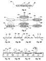
- FIG. 1is a perspective view of an exemplary embodiment of a semiconductor device incorporating teachings of the present invention, which semiconductor device includes a spacer layer on an active surface thereof;
- FIG. 2is a cross-section taken along line 2 - 2 of FIG. 1 ;
- FIG. 3is a perspective view illustrating another, inverted semiconductor device according to the present invention, which includes a spacer layer on a back side thereof;
- FIG. 4is a side view that depicts a semiconductor device with spacer layers on both an active surface and a back side thereof;
- FIG. 5schematically depicts the use of screen printing techniques to form the spacers of a spacer layer on a semiconductor device
- FIGS. 6A-6Dare schematic representations of the use of semiconductor device fabrication processes to form the spacers of a spacer layer on a semiconductor device
- FIGS. 7A-7Dschematically illustrate formation of the spacers of a spacer layer on a semiconductor device by way of stereolithography
- FIG. 8schematically depicts the formation of spacers by way of a dispensing process
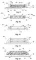
- FIG. 9is a cross-sectional representation of a stacked assembly that includes the semiconductor device of FIGS. 1 and 2 ;
- FIGS. 9A and 9Bschematically represent an embodiment of semiconductor device to be used in a stacked assembly and that includes spacers formed over portions of discrete conductive elements that protrude over the active surface thereof;
- FIG. 9Cis a cross-sectional representation of another embodiment of stacked semiconductor device assembly that includes the semiconductor device of FIGS. 1 and 2 ;
- FIG. 10is a side view of another stacked assembly, which includes a semiconductor device of the type shown in FIGS. 1 and 2 with a semiconductor device of the type illustrated in FIG. 3 stacked thereon;
- FIG. 11is a side view of a stacked assembly including more than two semiconductor devices in stacked arrangement.
- FIG. 12is a cross-sectional representation of a package including an assembly of the present invention.
- Semiconductor device 10includes a spacer layer 20 on an active surface 12 thereof.
- Spacer layer 20is positioned on active surface 12 or configured such that bond pads 16 of semiconductor device 10 are exposed beyond an outer periphery of spacer layer 20 or are otherwise accessible to equipment for forming or positioning discrete conductive elements (e.g., a wire bonding capillary, thermocompression bonding equipment, etc.).
- discrete conductive elementse.g., a wire bonding capillary, thermocompression bonding equipment, etc.
- spacer layer 20includes a plurality of discrete, laterally spaced apart solid regions, which are referred to herein as spacers 22 , and voids 24 that are located between adjacent spacers 22 .
- spacers 22are depicted in FIGS. 1 and 2 as being laterally offset from bond pads 16 , if formed following the connection of discrete conductive elements 18 (see, e.g., FIG. 10 ) to bond pads 16 , any suitable embodiment of spacer 22 incorporating teachings of the present invention may be formed over bond pads 16 , as well as the portions of discrete conductive elements 18 that are proximate thereto. Due to the presence of voids 24 in spacer layer 20 , spacer layer 20 covers only portions of active surface 12 .
- Voids 24are configured and arranged to receive an underfill or encapsulant material, which may, at least in part, secure semiconductor device 10 to another at least partially superimposed semiconductor device 110 ( FIG. 9 ).
- an underfill or encapsulant materialwhich may, at least in part, secure semiconductor device 10 to another at least partially superimposed semiconductor device 110 ( FIG. 9 ).
- Other nonconfluent configurations of spacer layers that are configured to permit an adhesive material to flow laterally thereinto and thereby substantially fill voids in the spacer layerare also within the scope of the present invention.
- Spacers 22 and voids 24 of spacer layer 20may be arranged randomly or in a pattern.
- the configurations of spacers 22 and voids 24may facilitate the introduction of an underfill or encapsulant material into voids 24 while reducing or eliminating the incidence of void or bubble formation in the underfill or encapsulant material.
- Spacers 22may be substantially identically configured or have different configurations.
- spacers 22may have substantially planar upper surfaces and cross-sectional shapes taken along the length thereof including, but not limited to, round shapes (e.g., circular, ovals, ellipsoids, etc.), polygonal shapes (e.g., triangular, square, diamond-shaped, rectangular, hexagonal, octagonal, etc.) (see FIG. 4 ), crosses, elongate members which may be straight, bent, or curved, and other shapes.
- the upper surfaces of spacers 22may be nonplanar, such as cones, pyramids, the depicted domes, or other suitable shapes.
- Spacers 22may comprise solid or at least partially hollow members.
- FIG. 3illustrates another embodiment of semiconductor device 10 ′, which includes a spacer layer 20 on a back side 14 ′ thereof.
- Spacer layer 20may include any combination of features described above with reference to FIGS. 1 and 2 .
- semiconductor device 10 ′′includes spacer layers 20 on both an active surface 12 ′′ and a back side 14 ′′ thereof.
- FIGS. 5-8illustrate exemplary methods by which spacer layers 20 and their spacers 22 may be fabricated.
- FIG. 5schematically depicts the use of a screen printing process in which a spacer layer 20 is formed on a semiconductor device 10 ′′′, shown in the form of a wafer including a plurality of devices fabricated thereon.
- a screen 210 of a known type with a spacer pattern 220 thereinis positioned over and aligned with semiconductor device 10 ′′′.
- Spacer pattern 220includes apertures 222 through which regions of an active surface 12 ′′′ of semiconductor device 10 ′′′ are exposed.
- a quantity of a suitable spacer material 215is then placed on screen 210 and spread thereacross, causing some of spacer material 215 to fill apertures 222 and adhere to active surface 12 ′′′.
- Screen 210may then be removed from semiconductor device 10 ′′′, with spacer material 215 that remains on active surface 12 ′′′ forming spacers 22 of spacer layer 20 .
- the material of spacers 22may be cured or otherwise hardened by a process (e.g., thermally, by irradiation, by cooling, etc.) or combination of processes that is suitable for the particular type of spacer material 215 employed.
- FIGS. 6A-6DA method in which conventional semiconductor device fabrication processes are used to form spacers 22 of spacer layer 20 is illustrated in FIGS. 6A-6D .
- a layer 220 ′ of a material suitable for use as spacers 22( FIG. 6D ) is formed over an active surface 12 of a semiconductor device 10 .
- Known processese.g., spreading, exposure, and developing of a photoimageable polymer
- Solid regions 231 of mask 230cover portions of layer 220 ′ that will subsequently form spacers 22 of spacer layer 20 ( FIG. 6D ), while other regions of layer 220 ′, which are to be removed, are exposed through apertures 232 of mask 230 .
- Semiconductor device 10 and mask 230may then be exposed to an etchant that will remove the material of layer 220 ′ in regions thereof that are exposed through apertures 232 , as depicted in FIG. 6C .
- an etchantthat will remove the material of layer 220 ′ in regions thereof that are exposed through apertures 232 , as depicted in FIG. 6C .
- spacers 22 of spacer layer 20are formed.
- Mask 230may be removed from spacer layer 20 by known processes (e.g., use of a suitable resist strip when mask 230 comprises a photomask).
- FIGS. 7A-7Dschematically depict an exemplary stereolithography process for fabricating spacer layer 20 ( FIG. 7D ) on an active surface 12 of a semiconductor device 10 .
- active surface 12 of semiconductor device 10may be submerged beneath a quantity of unconsolidated material 213 ′′ (e.g., a liquid photoimageable polymer), which forms a layer 215 ′′ over active surface 12 .
- unconsolidated material 213 ′′e.g., a liquid photoimageable polymer
- FIG. 7Bselected regions of layer 215 ′′ are at least partially consolidated, as known in the art (e.g., by exposure of a liquid photoimageable polymer to curing radiation, such as a laser beam 235 ).
- each spacer 22includes two sublayers 22 a , 22 b , although stereolithographically fabricated spacers 22 having single layers or other numbers of sublayers are also within the scope of the present invention.
- spacers 22may be formed by dispensing small, laterally discrete quantities of a spacer material, such as a polymer (e.g, an epoxy, thermoplastic polymer, etc.), directly onto an active surface 12 of a semiconductor device 10 that is singulated or part of a wafer, partial wafer, or other large-scale fabrication substrate.
- a spacer materialsuch as a polymer (e.g, an epoxy, thermoplastic polymer, etc.)
- a spacer materialsuch as a polymer (e.g, an epoxy, thermoplastic polymer, etc.)
- spacers 22 of spacer layers 20are formed depends at least in part upon the particular materials used to form spacers 22 .
- an assembly 30is depicted that includes a substrate 40 , a first semiconductor device 10 , and a second semiconductor device 110 stacked on first semiconductor device 10 .
- Discrete conductive elements 18electrically connect bond pads 16 of first semiconductor device 10 to corresponding contact areas 46 of substrate 40 .
- Second semiconductor device 110may overlie at least some bond pads 16 of first semiconductor device 10 , as well as any discrete conductive elements 18 extending therefrom.
- First semiconductor device 10 and second semiconductor device 110are separated from one another by way of spacers 22 located therebetween.
- substrate 40is depicted as an interposer of which contact areas 46 are bond pads located on a top side 44 thereof, other types of substrates are also within the scope of the present invention, including, without limitation, circuit boards, other semiconductor devices, and leads.
- first semiconductor device 10is secured to substrate 40 by way of a suitable adhesive material 15 , such as a thermoplastic resin, a silicon-filled thermoplastic resin, a thermoset resin, an epoxy, a silicone, a silcone-carbon resin, a polyimide, a polyurethane, or a parylene.
- a suitable adhesive material 15such as a thermoplastic resin, a silicon-filled thermoplastic resin, a thermoset resin, an epoxy, a silicone, a silcone-carbon resin, a polyimide, a polyurethane, or a parylene.
- first semiconductor device 10may be secured to or otherwise associated with a substrate in a different manner, depending upon the particular type of substrate employed.
- leadsmay extend partially over and be secured to active surface 12 of first semiconductor device 10 .
- Such leadsmay extend over corresponding bond pads 16 and be secured thereto directly (e.g., by thermocompression bonds) or by way of conductive joints (e.g., balls, bumps, pillars, columns, or other structures of a metal or metal alloy, such as solder, a conductive epoxy, a conductor-filled epoxy, or a z-axis conductive elastomer).
- conductive jointse.g., balls, bumps, pillars, columns, or other structures of a metal or metal alloy, such as solder, a conductive epoxy, a conductor-filled epoxy, or a z-axis conductive elastomer.
- discrete conductive elementssuch as bond wires or TAB elements may be positioned or formed between each lead and its corresponding bond pad 16 to electrically connect the same.
- the heights of spacers 22may be greater than the distance discrete conductive elements 18 protrude above active surface 12 of first semiconductor device 10 , thereby preventing discrete conductive elements 18 from electrically shorting on a back side 114 of the overlying second semiconductor device 110 .
- the heights of spacers 22may be about the same as or even smaller than the distances discrete conductive elements 18 protrude above active surface 12 , so long as the heights of spacers 22 and the combined strengths of discrete conductive elements 18 over which second semiconductor device 110 is positioned prevent discrete conductive elements 18 from being damaged (e.g., by being bent, kinked, or otherwise deformed) or from collapsing onto one another. If the heights of spacers 22 are less than the distance discrete conductive elements 18 protrude above active surface 12 , it is preferred that portions of discrete conductive elements 18 and back side 114 that may contact one another be electrically isolated from each other.
- discrete conductive elements 18may include a dielectric coating 19 thereon.
- all or part of back side 114may include a dielectric coating 116 .
- Suitable dielectric materials for both dielectric coating 19 and dielectric coating 116include, but are not limited to, nonconductive polymers, glass, silicon oxide, silicon nitride, and silicon oxynitride, as well as nonconductive oxides of the respective discrete conductive element 18 or second semiconductor device 110 material.
- An adhesive material 115such as a thermoset resin, a UV-curable material, a thermoplastic resin, a silicone, a silicone-carbon resin, a polyimide, a polyurethane, a parylene, or the like, may be located between active surface 12 of first semiconductor device 10 and back side 114 of second semiconductor device 110 , securing first and second semiconductor devices 10 and 110 to one another.
- a partial assembly 30 ′′′is shown that includes a semiconductor device 10 ′′′ positioned over and secured to a substrate 40 .
- Discrete conductive elements 18such as bond wires, electrically connect bond pads 16 of semiconductor device 10 ′′′ to corresponding contact areas 46 of substrate 40 .
- Spacers 22 ′′′are formed over portions of discrete conductive elements 18 and may support and/or protect discrete conductive elements 18 as a second semiconductor device (not shown) is subsequently assembled thereover. While each spacer 22 ′′′ is depicted in FIG.
- FIG. 9Cdepicts an assembly 130 that includes first and second semiconductor devices 10 , 110 , as well as spacers 22 and adhesive material 115 therebetween, that are similar to those of assembly 30 depicted in FIG. 9 .
- Assembly 130differs from assembly 30 in that substrate 140 comprises leads 142 .
- leads 142are of a leads-over-chip (LOC) configuration and, thus, extend partially over and are secured to an active surface 12 of first semiconductor device 10 .
- leads 142are positioned at least partially over and bonded to corresponding bond pads 16 of first semiconductor device 10 .
- LOCleads-over-chip
- leads 142may be bonded to corresponding bond pads 16 by way of thermocompression bonds or by the use of a conductive adhesive material, such as solder, another metal or metal alloy, conductive or conductor-filled epoxy, an anisotropically conductive elastomer, or the like, between leads 142 and bond pads 16 .
- a conductive adhesive materialsuch as solder, another metal or metal alloy, conductive or conductor-filled epoxy, an anisotropically conductive elastomer, or the like, between leads 142 and bond pads 16 .
- LOC type leads 142may communicate with corresponding bond pads 16 by way of discrete conductive elements (e.g., bond wires, TAB elements, etc.).
- Other variations of the assemblies depicted hereinmay include substrates that comprise other types of leads, circuit boards, an additional semiconductor device, or the like.
- FIG. 10another embodiment of assembly 30 ′ includes a first semiconductor device 10 with a second semiconductor device 10 ′ stacked thereon.
- first semiconductor device 10includes a spacer layer 20 on active surface 12 thereof and second semiconductor device 10 ′ includes a spacer layer 20 on a back side 14 ′ thereof (see also FIG. 3 ), spacer layers 20 are positioned adjacent to one another. At least some spacers 22 of the adjacent spacer layers 20 abut each other, with the combined heights of abutting spacers 22 defining the distance between first semiconductor device 10 and second semiconductor device 10 ′.
- FIG. 11illustrates such an assembly 30 ′′, which includes a substrate 40 and three semiconductor devices 10 , 110 in stacked arrangement thereon.
- an exemplary process for forming assembly 30includes securing a first semiconductor device 10 to a substrate 40 .
- an adhesive material 15is used, although other known methods for securing semiconductor devices to substrates are also within the scope of the present invention.
- Known processesmay be used to form or position discrete conductive elements 18 , such as TAB elements, thermocompression bonded leads, the depicted bond wires, or the like, between bond pads 16 of first semiconductor device 10 and corresponding contact areas 46 of substrate 40 .
- Spacers 22may be formed on regions of active surface 12 of semiconductor device 10 by known processes, such as those described previously herein with reference to FIGS. 5-8 .
- spacers 22may be effected before or after first semiconductor device 10 is secured to substrate 40 , as well as before or after the formation of discrete conductive elements 18 .
- a second semiconductor device 110is positioned over spacers 22 , with a back side 114 thereof resting against spacers 22 .
- a suitable adhesive material 115such as a known underfill material, may be introduced into voids 24 of spacer layer 20 , between active surface 12 of first semiconductor device 10 and back side 114 of second semiconductor device 110 .
- spacers 22may prevent discrete conductive elements 18 from being collapsed onto one another, bent, kinked, or otherwise distorted or damaged during the introduction of adhesive material 115 between first and second semiconductor devices 10 and 110 .
- One or more known processesmay be used to at least partially cure or otherwise harden adhesive material 115 .
- Spacers 22 that at least partially encapsulate discrete conductive elements 18may also electrically isolate discrete conductive elements 18 from the back side 114 of an adjacent semiconductor device 110 .
- a relatively high viscosity adhesive material 115may be applied to a surface of one or both of first and second semiconductor devices 10 and 110 prior to assembly thereof with one another. Then, when first and second semiconductor devices 10 and 110 are assembled, adhesive material 115 fills voids 24 of spacer layer 20 and contacts opposed surfaces (e.g., active surface 12 and back side 114 , respectively) of first semiconductor device 10 and second semiconductor device 110 . Following the assembly of first semiconductor device 10 and second semiconductor device 110 , one or more known processes may be used to at least partially cure or otherwise harden adhesive material 115 .
- a package 50may include any assembly (e.g., assemblies 30 , 30 ′, 30 ′′) according to the present invention.
- package 50includes assembly 30 , as well as an encapsulant 52 substantially filling voids 24 in spacer layer 20 and surrounding first and second semiconductor devices 10 and 110 , discrete conductive elements 18 , and portions of substrate 40 that are located adjacent to first semiconductor device 10 .
- encapsulant 52may be formed separately from a layer of adhesive material 115 (see, e.g., FIG. 9 ) between first semiconductor device 10 and second semiconductor device 110 .
- encapsulant 52is depicted as being formed by transfer molding processes or by pot molding processes and, thus, from appropriate compounds (e.g., a silicon-filled thermoplastic resin for transfer molding or an epoxy for pot molding), other encapsulation techniques, such as glob top processes, and appropriate materials may also be used to form encapsulant 52 .
- encapsulant 52may be formed separately from the layer of adhesive material 115 between first and second semiconductor devices 10 and 110 , the same or similar materials may be used as adhesive material 115 and to form encapsulant 52 .
- adhesive material 115 and/or the material of encapsulant 52may comprise the same or a similar material to that from which spacers 22 are formed. Use of the same or similar materials for these elements may optimize adhesion and provide for a matched coefficient of thermal expansion (CTE).
- CTEcoefficient of thermal expansion
- Package 50may also include external connective elements 54 electrically coupled to corresponding contact areas 46 by vias and/or conductive traces (not shown) carried by substrate 40 , as known in the art.
- External connective elements 54may, by way of example only, comprise conductive plug-in type connectors, pin connectors, conductive or conductor-filled epoxy pillars, an anisotropically conductive adhesive, the depicted conductive bumps, or any other conductive structures that are suitable for interconnecting assembly 30 with other, external electronic components.
Landscapes
- Engineering & Computer Science (AREA)
- Microelectronics & Electronic Packaging (AREA)
- Power Engineering (AREA)
- Physics & Mathematics (AREA)
- Condensed Matter Physics & Semiconductors (AREA)
- General Physics & Mathematics (AREA)
- Computer Hardware Design (AREA)
- Manufacturing & Machinery (AREA)
- Structures Or Materials For Encapsulating Or Coating Semiconductor Devices Or Solid State Devices (AREA)
Abstract
Description
Claims (43)
Priority Applications (3)
| Application Number | Priority Date | Filing Date | Title |
|---|---|---|---|
| US09/939,253US7518223B2 (en) | 2001-08-24 | 2001-08-24 | Semiconductor devices and semiconductor device assemblies including a nonconfluent spacer layer |
| US10/225,973US20030038357A1 (en) | 2001-08-24 | 2002-08-22 | Spacer for semiconductor devices, semiconductor devices and assemblies including the spacer, and methods |
| US11/216,600US20060035408A1 (en) | 2001-08-24 | 2005-08-31 | Methods for designing spacers for use in stacking semiconductor devices or semiconductor device components |
Applications Claiming Priority (1)
| Application Number | Priority Date | Filing Date | Title |
|---|---|---|---|
| US09/939,253US7518223B2 (en) | 2001-08-24 | 2001-08-24 | Semiconductor devices and semiconductor device assemblies including a nonconfluent spacer layer |
Related Child Applications (1)
| Application Number | Title | Priority Date | Filing Date |
|---|---|---|---|
| US10/225,973DivisionUS20030038357A1 (en) | 2001-08-24 | 2002-08-22 | Spacer for semiconductor devices, semiconductor devices and assemblies including the spacer, and methods |
Publications (2)
| Publication Number | Publication Date |
|---|---|
| US20030038355A1 US20030038355A1 (en) | 2003-02-27 |
| US7518223B2true US7518223B2 (en) | 2009-04-14 |
Family
ID=25472828
Family Applications (3)
| Application Number | Title | Priority Date | Filing Date |
|---|---|---|---|
| US09/939,253Expired - LifetimeUS7518223B2 (en) | 2001-08-24 | 2001-08-24 | Semiconductor devices and semiconductor device assemblies including a nonconfluent spacer layer |
| US10/225,973AbandonedUS20030038357A1 (en) | 2001-08-24 | 2002-08-22 | Spacer for semiconductor devices, semiconductor devices and assemblies including the spacer, and methods |
| US11/216,600AbandonedUS20060035408A1 (en) | 2001-08-24 | 2005-08-31 | Methods for designing spacers for use in stacking semiconductor devices or semiconductor device components |
Family Applications After (2)
| Application Number | Title | Priority Date | Filing Date |
|---|---|---|---|
| US10/225,973AbandonedUS20030038357A1 (en) | 2001-08-24 | 2002-08-22 | Spacer for semiconductor devices, semiconductor devices and assemblies including the spacer, and methods |
| US11/216,600AbandonedUS20060035408A1 (en) | 2001-08-24 | 2005-08-31 | Methods for designing spacers for use in stacking semiconductor devices or semiconductor device components |
Country Status (1)
| Country | Link |
|---|---|
| US (3) | US7518223B2 (en) |
Cited By (7)
| Publication number | Priority date | Publication date | Assignee | Title |
|---|---|---|---|---|
| US20080303109A1 (en)* | 2006-05-22 | 2008-12-11 | Visera Technologies Co. Ltd. R.O.C. | Optoelectronic device chip having a composite spacer structure and method making same |
| US20090014857A1 (en)* | 2007-07-13 | 2009-01-15 | Erich Hufgard | Semiconductor wafer structure |
| US20110062598A1 (en)* | 2006-07-11 | 2011-03-17 | Atmel Corporation | Stacked-die package including substrate-ground coupling |
| US8927332B2 (en) | 2006-02-20 | 2015-01-06 | Micron Technology, Inc. | Methods of manufacturing semiconductor device assemblies including face-to-face semiconductor dice |
| US20160260691A1 (en)* | 2013-10-07 | 2016-09-08 | Toyota Jidosha Kabushiki Kaisha | Semiconductor module |
| US10099439B2 (en)* | 2012-11-14 | 2018-10-16 | Ehs Lens Philippines, Inc. | Method of manufacturing polarizing plastic lens |
| US20230008716A1 (en)* | 2003-08-29 | 2023-01-12 | Micron Technology, Inc. | Stacked microfeature devices and associated methods |
Families Citing this family (79)
| Publication number | Priority date | Publication date | Assignee | Title |
|---|---|---|---|---|
| KR100401020B1 (en)* | 2001-03-09 | 2003-10-08 | 앰코 테크놀로지 코리아 주식회사 | Stacking structure of semiconductor chip and semiconductor package using it |
| US20030042615A1 (en)* | 2001-08-30 | 2003-03-06 | Tongbi Jiang | Stacked microelectronic devices and methods of fabricating same |
| CN1251318C (en)* | 2002-02-25 | 2006-04-12 | 精工爱普生株式会社 | Semiconductor water, semiconductor device and their producing method, circuit board and instrument |
| US6885093B2 (en)* | 2002-02-28 | 2005-04-26 | Freescale Semiconductor, Inc. | Stacked die semiconductor device |
| DE10223738B4 (en)* | 2002-05-28 | 2007-09-27 | Qimonda Ag | Method for connecting integrated circuits |
| JP3576540B2 (en)* | 2002-08-19 | 2004-10-13 | 沖電気工業株式会社 | Multi-chip package |
| US6969914B2 (en)* | 2002-08-29 | 2005-11-29 | Micron Technology, Inc. | Electronic device package |
| DE10310617B4 (en)* | 2003-03-10 | 2006-09-21 | Infineon Technologies Ag | Electronic component with cavity and a method for producing the same |
| JP2004312008A (en)* | 2003-04-08 | 2004-11-04 | Samsung Electronics Co Ltd | Semiconductor multi-chip package and method of manufacturing the same |
| KR20040087501A (en)* | 2003-04-08 | 2004-10-14 | 삼성전자주식회사 | A package of a semiconductor chip with center pads and packaging method thereof |
| KR100506035B1 (en)* | 2003-08-22 | 2005-08-03 | 삼성전자주식회사 | Semiconductor package and manufacturing method thereof |
| US20050056946A1 (en)* | 2003-09-16 | 2005-03-17 | Cookson Electronics, Inc. | Electrical circuit assembly with improved shock resistance |
| US20050110126A1 (en)* | 2003-11-25 | 2005-05-26 | Kai-Chiang Wu | Chip adhesive |
| US7306971B2 (en)* | 2004-03-02 | 2007-12-11 | Chippac Inc. | Semiconductor chip packaging method with individually placed film adhesive pieces |
| US7074695B2 (en)* | 2004-03-02 | 2006-07-11 | Chippac, Inc. | DBG system and method with adhesive layer severing |
| US20050208700A1 (en)* | 2004-03-19 | 2005-09-22 | Chippac, Inc. | Die to substrate attach using printed adhesive |
| US20050224959A1 (en)* | 2004-04-01 | 2005-10-13 | Chippac, Inc | Die with discrete spacers and die spacing method |
| US7190058B2 (en)* | 2004-04-01 | 2007-03-13 | Chippac, Inc. | Spacer die structure and method for attaching |
| US20050224919A1 (en)* | 2004-04-01 | 2005-10-13 | Chippac, Inc | Spacer die structure and method for attaching |
| US20050258545A1 (en)* | 2004-05-24 | 2005-11-24 | Chippac, Inc. | Multiple die package with adhesive/spacer structure and insulated die surface |
| US20050269692A1 (en)* | 2004-05-24 | 2005-12-08 | Chippac, Inc | Stacked semiconductor package having adhesive/spacer structure and insulation |
| US8552551B2 (en)* | 2004-05-24 | 2013-10-08 | Chippac, Inc. | Adhesive/spacer island structure for stacking over wire bonded die |
| US20050258527A1 (en)* | 2004-05-24 | 2005-11-24 | Chippac, Inc. | Adhesive/spacer island structure for multiple die package |
| SG119234A1 (en)* | 2004-07-29 | 2006-02-28 | Micron Technology Inc | Assemblies including stacked semiconductor dice having centrally located wire bonded bond pads |
| US7492039B2 (en)* | 2004-08-19 | 2009-02-17 | Micron Technology, Inc. | Assemblies and multi-chip modules including stacked semiconductor dice having centrally located, wire bonded bond pads |
| DE102004037610B3 (en)* | 2004-08-03 | 2006-03-16 | Infineon Technologies Ag | Integrated circuit connection method e.g. for substrate and circuit assembly, involves planning flexible intermediate layer on integrated circuit and or substrate with flexible layer structured in raised and lower ranges |
| WO2006061673A1 (en)* | 2004-12-09 | 2006-06-15 | Infineon Technologies Ag | Semiconductor package having at least two semiconductor chips and method of assembling the semiconductor package |
| EP1688997B1 (en)* | 2005-02-02 | 2014-04-16 | Infineon Technologies AG | Electronic component with stacked semiconductor chips |
| US7147447B1 (en)* | 2005-07-27 | 2006-12-12 | Texas Instruments Incorporated | Plastic semiconductor package having improved control of dimensions |
| DE102005036324A1 (en)* | 2005-07-29 | 2006-09-28 | Infineon Technologies Ag | Semiconductor device for use as digital memory device, has semiconductor chip comprising bond wire guiding unit in edge area of top side of chip, where guiding unit has structures for guiding bond wire |
| TWI268628B (en)* | 2005-08-04 | 2006-12-11 | Advanced Semiconductor Eng | Package structure having a stacking platform |
| US20070045807A1 (en)* | 2005-09-01 | 2007-03-01 | Micron Technology, Inc. | Microelectronic devices and methods for manufacturing microelectronic devices |
| US20070070608A1 (en)* | 2005-09-29 | 2007-03-29 | Skyworks Solutions, Inc. | Packaged electronic devices and process of manufacturing same |
| DE102005050127B3 (en)* | 2005-10-18 | 2007-05-16 | Infineon Technologies Ag | Method for applying a structure of joining material to the backs of semiconductor chips |
| US20070178666A1 (en)* | 2006-01-31 | 2007-08-02 | Stats Chippac Ltd. | Integrated circuit system with waferscale spacer system |
| US8810018B2 (en)* | 2006-02-03 | 2014-08-19 | Stats Chippac Ltd. | Stacked integrated circuit package system with face to face stack configuration |
| US7675180B1 (en) | 2006-02-17 | 2010-03-09 | Amkor Technology, Inc. | Stacked electronic component package having film-on-wire spacer |
| US20070231970A1 (en)* | 2006-03-31 | 2007-10-04 | Tsuyoshi Fukuo | Cured mold compound spacer for stacked-die package |
| US7829986B2 (en) | 2006-04-01 | 2010-11-09 | Stats Chippac Ltd. | Integrated circuit package system with net spacer |
| US7443037B2 (en)* | 2006-04-01 | 2008-10-28 | Stats Chippac Ltd. | Stacked integrated circuit package system with connection protection |
| US7633144B1 (en) | 2006-05-24 | 2009-12-15 | Amkor Technology, Inc. | Semiconductor package |
| JP2008004570A (en)* | 2006-06-20 | 2008-01-10 | Matsushita Electric Ind Co Ltd | Resin-sealed semiconductor device manufacturing method, resin-sealed semiconductor device manufacturing apparatus, and resin-sealed semiconductor device |
| US20080054429A1 (en)* | 2006-08-25 | 2008-03-06 | Bolken Todd O | Spacers for separating components of semiconductor device assemblies, semiconductor device assemblies and systems including spacers and methods of making spacers |
| KR100809701B1 (en)* | 2006-09-05 | 2008-03-06 | 삼성전자주식회사 | Multichip Package with Interchip Chip Blocks |
| DE102006043215A1 (en)* | 2006-09-11 | 2008-03-27 | Qimonda Ag | Chip i.e. semiconductor chip, coplanar installing method, involves connecting adhesive surfaces with each other by chip and support under adjusting of intermediate area between chip and support |
| US8154881B2 (en)* | 2006-11-13 | 2012-04-10 | Telecommunication Systems, Inc. | Radiation-shielded semiconductor assembly |
| US20080128879A1 (en)* | 2006-12-01 | 2008-06-05 | Hem Takiar | Film-on-wire bond semiconductor device |
| US20080131998A1 (en)* | 2006-12-01 | 2008-06-05 | Hem Takiar | Method of fabricating a film-on-wire bond semiconductor device |
| SG143098A1 (en)* | 2006-12-04 | 2008-06-27 | Micron Technology Inc | Packaged microelectronic devices and methods for manufacturing packaged microelectronic devices |
| US8723332B2 (en)* | 2007-06-11 | 2014-05-13 | Invensas Corporation | Electrically interconnected stacked die assemblies |
| TW200917391A (en)* | 2007-06-20 | 2009-04-16 | Vertical Circuits Inc | Three-dimensional circuitry formed on integrated circuit device using two-dimensional fabrication |
| US7969023B2 (en)* | 2007-07-16 | 2011-06-28 | Stats Chippac Ltd. | Integrated circuit package system with triple film spacer having embedded fillers and method of manufacture thereof |
| WO2009035849A2 (en) | 2007-09-10 | 2009-03-19 | Vertical Circuits, Inc. | Semiconductor die mount by conformal die coating |
| US20090072373A1 (en)* | 2007-09-14 | 2009-03-19 | Reynaldo Corpuz Javier | Packaged integrated circuits and methods to form a stacked integrated circuit package |
| CN101999167B (en) | 2008-03-12 | 2013-07-17 | 伊文萨思公司 | Support mounted electrically interconnected die assembly |
| US7863159B2 (en)* | 2008-06-19 | 2011-01-04 | Vertical Circuits, Inc. | Semiconductor die separation method |
| US9153517B2 (en) | 2008-05-20 | 2015-10-06 | Invensas Corporation | Electrical connector between die pad and z-interconnect for stacked die assemblies |
| WO2010151578A2 (en)* | 2009-06-26 | 2010-12-29 | Vertical Circuits, Inc. | Electrical interconnect for die stacked in zig-zag configuration |
| JP5619381B2 (en)* | 2009-07-09 | 2014-11-05 | ピーエスフォー ルクスコ エスエイアールエルPS4 Luxco S.a.r.l. | Semiconductor device and manufacturing method of semiconductor device |
| US8102038B2 (en)* | 2009-09-18 | 2012-01-24 | Texas Instruments Incorporated | Semiconductor chip attach configuration having improved thermal characteristics |
| JP2011077108A (en)* | 2009-09-29 | 2011-04-14 | Elpida Memory Inc | Semiconductor device |
| WO2011056668A2 (en) | 2009-10-27 | 2011-05-12 | Vertical Circuits, Inc. | Selective die electrical insulation additive process |
| TWI544604B (en) | 2009-11-04 | 2016-08-01 | 英維瑟斯公司 | Stacked die assembly having reduced stress electrical interconnects |
| WO2011133746A1 (en) | 2010-04-21 | 2011-10-27 | Empire Technology Development Llc | Precision spacing for stacked wafer assemblies |
| JP5673423B2 (en)* | 2011-08-03 | 2015-02-18 | 富士通セミコンダクター株式会社 | Semiconductor device and manufacturing method of semiconductor device |
| DE102014008838B4 (en)* | 2014-06-20 | 2021-09-30 | Kunststoff-Zentrum In Leipzig Gemeinnützige Gmbh | Stress-reducing flexible connecting element for a microelectronic system |
| US9490195B1 (en) | 2015-07-17 | 2016-11-08 | Invensas Corporation | Wafer-level flipped die stacks with leadframes or metal foil interconnects |
| US9871019B2 (en) | 2015-07-17 | 2018-01-16 | Invensas Corporation | Flipped die stack assemblies with leadframe interconnects |
| US9825002B2 (en) | 2015-07-17 | 2017-11-21 | Invensas Corporation | Flipped die stack |
| US10163871B2 (en) | 2015-10-02 | 2018-12-25 | Qualcomm Incorporated | Integrated device comprising embedded package on package (PoP) device |
| US9947642B2 (en)* | 2015-10-02 | 2018-04-17 | Qualcomm Incorporated | Package-on-Package (PoP) device comprising a gap controller between integrated circuit (IC) packages |
| US9508691B1 (en) | 2015-12-16 | 2016-11-29 | Invensas Corporation | Flipped die stacks with multiple rows of leadframe interconnects |
| US10566310B2 (en) | 2016-04-11 | 2020-02-18 | Invensas Corporation | Microelectronic packages having stacked die and wire bond interconnects |
| US9595511B1 (en) | 2016-05-12 | 2017-03-14 | Invensas Corporation | Microelectronic packages and assemblies with improved flyby signaling operation |
| US9728524B1 (en) | 2016-06-30 | 2017-08-08 | Invensas Corporation | Enhanced density assembly having microelectronic packages mounted at substantial angle to board |
| JP6669104B2 (en)* | 2017-03-03 | 2020-03-18 | 株式会社デンソー | Semiconductor device |
| US11552051B2 (en) | 2017-04-01 | 2023-01-10 | Intel Corporation | Electronic device package |
| US11127604B2 (en)* | 2018-01-05 | 2021-09-21 | Innolux Corporation | Manufacturing method of semiconductor device |
| KR20220040849A (en)* | 2020-09-24 | 2022-03-31 | 삼성전자주식회사 | image sensor package for improving reliability |
Citations (81)
| Publication number | Priority date | Publication date | Assignee | Title |
|---|---|---|---|---|
| US3811186A (en) | 1972-12-11 | 1974-05-21 | Ibm | Method of aligning and attaching circuit devices on a substrate |
| US4184043A (en) | 1977-05-02 | 1980-01-15 | U.S. Philips Corporation | Method of providing spacers on an insulating substrate |
| JPH01185952A (en) | 1988-01-21 | 1989-07-25 | Oki Electric Ind Co Ltd | Flip-chip type semiconductor device |
| US5037779A (en) | 1989-05-19 | 1991-08-06 | Whalley Peter D | Method of encapsulating a sensor device using capillary action and the device so encapsulated |
| US5056215A (en) | 1990-12-10 | 1991-10-15 | Delco Electronics Corporation | Method of providing standoff pillars |
| US5220200A (en)* | 1990-12-10 | 1993-06-15 | Delco Electronics Corporation | Provision of substrate pillars to maintain chip standoff |
| US5251806A (en) | 1990-06-19 | 1993-10-12 | International Business Machines Corporation | Method of forming dual height solder interconnections |
| JPH0621328A (en)* | 1992-07-03 | 1994-01-28 | Seiko Epson Corp | Semiconductor element mounting method |
| US5296738A (en) | 1991-07-08 | 1994-03-22 | Motorola, Inc. | Moisture relief for chip carrier |
| US5323060A (en) | 1993-06-02 | 1994-06-21 | Micron Semiconductor, Inc. | Multichip module having a stacked chip arrangement |
| US5331235A (en) | 1991-06-01 | 1994-07-19 | Goldstar Electron Co., Ltd. | Multi-chip semiconductor package |
| JPH0865579A (en)* | 1994-08-23 | 1996-03-08 | Olympus Optical Co Ltd | Solid state image pickup device |
| US5536362A (en) | 1992-11-17 | 1996-07-16 | Fujitsu Limited | Wire interconnect structures for connecting an integrated circuit to a substrate |
| JPH08288455A (en)* | 1995-04-11 | 1996-11-01 | Oki Electric Ind Co Ltd | Semiconductor device and its manufacture |
| US5684677A (en) | 1993-06-24 | 1997-11-04 | Kabushiki Kaisha Toshiba | Electronic circuit device |
| US5880017A (en) | 1994-08-08 | 1999-03-09 | Hewlett-Packard Co. | Method of bumping substrates by contained paste deposition |
| US5892417A (en) | 1996-12-27 | 1999-04-06 | Motorola Inc. | Saw device package and method |
| US5934545A (en) | 1997-02-21 | 1999-08-10 | Gordon; Thomas A. | Ball placement method and apparatus for forming a ball grid array |
| US6005778A (en) | 1995-06-15 | 1999-12-21 | Honeywell Inc. | Chip stacking and capacitor mounting arrangement including spacers |
| US6023217A (en) | 1998-01-08 | 2000-02-08 | Matsushita Electric Industrial Co., Ltd. | Resistor and its manufacturing method |
| USRE36613E (en) | 1993-04-06 | 2000-03-14 | Micron Technology, Inc. | Multi-chip stacked devices |
| JP2000101016A (en)* | 1998-09-18 | 2000-04-07 | Sharp Corp | Semiconductor integrated circuit device |
| US6049370A (en)* | 1993-01-26 | 2000-04-11 | Hughes Aircraft Company | Liquid crystal light valves using internal, fixed spacers and method of incorporating same |
| US6051886A (en) | 1995-08-16 | 2000-04-18 | Micron Technology, Inc. | Angularly offset stacked die multichip device and method of manufacture |
| US6063688A (en) | 1997-09-29 | 2000-05-16 | Intel Corporation | Fabrication of deep submicron structures and quantum wire transistors using hard-mask transistor width definition |
| US6071371A (en) | 1998-02-02 | 2000-06-06 | Delco Electronics Corporation | Method of simultaneously attaching surface-mount and chip-on-board dies to a circuit board |
| US6077380A (en)* | 1995-06-30 | 2000-06-20 | Microfab Technologies, Inc. | Method of forming an adhesive connection |
| US6080264A (en) | 1996-05-20 | 2000-06-27 | Micron Technology, Inc. | Combination of semiconductor interconnect |
| US6097097A (en) | 1996-08-20 | 2000-08-01 | Fujitsu Limited | Semiconductor device face-down bonded with pillars |
| US6098278A (en)* | 1994-06-23 | 2000-08-08 | Cubic Memory, Inc. | Method for forming conductive epoxy flip-chip on chip |
| US6130148A (en)* | 1997-12-12 | 2000-10-10 | Farnworth; Warren M. | Interconnect for semiconductor components and method of fabrication |
| JP2001056648A (en) | 1999-08-18 | 2001-02-27 | Ricoh Microelectronics Co Ltd | Production of printing plate for spacer formation and apparatus therefor, production of printing plate female die for spacer formation and apparatus therefor, spacer forming method and apparatus therefor, printing plate for spacer formation, printing plate female die for spacer formation and liquid crystal display device |
| US6212767B1 (en) | 1999-08-31 | 2001-04-10 | Micron Technology, Inc. | Assembling a stacked die package |
| US20010002066A1 (en) | 1998-03-18 | 2001-05-31 | Hitachi Cable Ltd. | Semiconductor device, lead-patterning substrate, and electronics device, and method for fabricating same |
| US6287895B1 (en) | 1999-01-29 | 2001-09-11 | Nec Corporation | Semiconductor package having enhanced ball grid array protective dummy members |
| US20010035587A1 (en)* | 2000-04-26 | 2001-11-01 | Mitsubishi Denki Kabushiki Kaisha | Resin-sealed chip stack type semiconductor device |
| US6313528B1 (en) | 1996-12-13 | 2001-11-06 | Tessera, Inc. | Compliant multichip package |
| US6316289B1 (en) | 1998-11-12 | 2001-11-13 | Amerasia International Technology Inc. | Method of forming fine-pitch interconnections employing a standoff mask |
| US6316786B1 (en)* | 1998-08-29 | 2001-11-13 | International Business Machines Corporation | Organic opto-electronic devices |
| US6333562B1 (en)* | 2000-07-13 | 2001-12-25 | Advanced Semiconductor Engineering, Inc. | Multichip module having stacked chip arrangement |
| US20020005491A1 (en)* | 2000-03-31 | 2002-01-17 | Takayuki Yagi | Electrooptic system array, charged-particle beam exposure apparatus using the same, and device manufacturing method |
| US6340846B1 (en)* | 2000-12-06 | 2002-01-22 | Amkor Technology, Inc. | Making semiconductor packages with stacked dies and reinforced wire bonds |
| US6351028B1 (en)* | 1999-02-08 | 2002-02-26 | Micron Technology, Inc. | Multiple die stack apparatus employing T-shaped interposer elements |
| US20020027630A1 (en) | 2000-06-30 | 2002-03-07 | Jun Yamada | Liquid crystal display element and method of producing the same |
| US20020036345A1 (en)* | 2000-09-27 | 2002-03-28 | Kabushiki Kaisha Toshiba | High frequency flip chip module and assembling method thereof |
| US20020056899A1 (en) | 1999-02-12 | 2002-05-16 | Junichi Hikita | Semiconductor chip and semiconductor device having a chip-on-chip structure |
| US20020068417A1 (en)* | 2000-06-08 | 2002-06-06 | Farnworth Warren M. | Stereolithographic method and apparatus for fabricating spacers for semiconductor devices and resulting structures |
| US20020070463A1 (en)* | 1994-05-09 | 2002-06-13 | Industrial Technology Research Institute | Composite bump bonding |
| US6410366B1 (en) | 1998-09-30 | 2002-06-25 | Seiko Epson Corporation | Semiconductor device and manufacturing method thereof, circuit board and electronic equipment |
| US20020079567A1 (en)* | 2000-12-22 | 2002-06-27 | Lo Randy H.Y. | Package structure stacking chips on front surface and back surface of substrate |
| US6424033B1 (en)* | 1999-08-31 | 2002-07-23 | Micron Technology, Inc. | Chip package with grease heat sink and method of making |
| US6437449B1 (en)* | 2001-04-06 | 2002-08-20 | Amkor Technology, Inc. | Making semiconductor devices having stacked dies with biased back surfaces |
| US20020151164A1 (en)* | 2001-04-12 | 2002-10-17 | Jiang Hunt Hang | Structure and method for depositing solder bumps on a wafer |
| US6472758B1 (en)* | 2000-07-20 | 2002-10-29 | Amkor Technology, Inc. | Semiconductor package including stacked semiconductor dies and bond wires |
| US20020167075A1 (en)* | 2001-05-14 | 2002-11-14 | Ruben Madrid | Carrier with metal bumps for semiconductor die packages |
| US20020177250A1 (en)* | 2001-03-26 | 2002-11-28 | Gazillion Bits, Inc. | Current confinement structure for vertical cavity surface emitting laser |
| US20020185746A1 (en)* | 2001-06-12 | 2002-12-12 | Park Sang Wook | Ball grid array IC package and manufacturing method thereof |
| US20020195697A1 (en) | 2001-06-21 | 2002-12-26 | Mess Leonard E. | Stacked mass storage flash memory package |
| US20030013643A1 (en)* | 2000-09-21 | 2003-01-16 | Wessels Michael R. | Prevention and treatment of streptococcal and staphylococcal infection |
| US20030015803A1 (en)* | 2001-07-20 | 2003-01-23 | Optosys Technologies Gmbh | High-density multichip module and method for manufacturing the same |
| US6521480B1 (en) | 1994-09-20 | 2003-02-18 | Tessera, Inc. | Method for making a semiconductor chip package |
| US20030038374A1 (en)* | 2001-08-27 | 2003-02-27 | Shim Jong Bo | Multi-chip package (MCP) with spacer |
| US20030038356A1 (en)* | 2001-08-24 | 2003-02-27 | Derderian James M | Semiconductor devices including stacking spacers thereon, assemblies including the semiconductor devices, and methods |
| US20030042615A1 (en)* | 2001-08-30 | 2003-03-06 | Tongbi Jiang | Stacked microelectronic devices and methods of fabricating same |
| US6531784B1 (en)* | 2000-06-02 | 2003-03-11 | Amkor Technology, Inc. | Semiconductor package with spacer strips |
| US6534345B1 (en) | 1999-02-26 | 2003-03-18 | Infineon Technologies Ag | Method for mounting a semiconductor chip on a carrier layer and device for carrying out the method |
| US6534391B1 (en) | 2001-08-17 | 2003-03-18 | Amkor Technology, Inc. | Semiconductor package having substrate with laser-formed aperture through solder mask layer |
| US6537852B2 (en)* | 2001-08-22 | 2003-03-25 | International Business Machines Corporation | Spacer - connector stud for stacked surface laminated multichip modules and methods of manufacture |
| US6552416B1 (en)* | 2000-09-08 | 2003-04-22 | Amkor Technology, Inc. | Multiple die lead frame package with enhanced die-to-die interconnect routing using internal lead trace wiring |
| US6593662B1 (en) | 2000-06-16 | 2003-07-15 | Siliconware Precision Industries Co., Ltd. | Stacked-die package structure |
| US20030178710A1 (en)* | 2002-03-21 | 2003-09-25 | Samsung Electronics Co., Ltd. | Semiconductor chip stack structure and method for forming the same |
| US6630730B2 (en) | 2000-04-28 | 2003-10-07 | Micron Technology, Inc. | Semiconductor device assemblies including interposers with dams protruding therefrom |
| US20030189259A1 (en)* | 2002-04-05 | 2003-10-09 | Nec Electronics Corporation | Semiconductor device and method for manufacturing the same |
| US6657290B2 (en)* | 2001-01-24 | 2003-12-02 | Sharp Kabushiki Kaisha | Semiconductor device having insulation layer and adhesion layer between chip lamination |
| US6682954B1 (en) | 1996-05-29 | 2004-01-27 | Micron Technology, Inc. | Method for employing piggyback multiple die #3 |
| US6724084B1 (en) | 1999-02-08 | 2004-04-20 | Rohm Co., Ltd. | Semiconductor chip and production thereof, and semiconductor device having semiconductor chip bonded to solid device |
| US6746894B2 (en) | 2001-03-30 | 2004-06-08 | Micron Technology, Inc. | Ball grid array interposer, packages and methods |
| US20040222509A1 (en)* | 2003-03-27 | 2004-11-11 | Seiko Epson Corporation | Semiconductor device, electronic device, electronic equipment and manufacturing method thereof |
| US20050077605A1 (en)* | 2003-10-08 | 2005-04-14 | United Microelectronics Corporation | Method and structure for a wafer level packaging |
| US20050104183A1 (en)* | 2003-11-17 | 2005-05-19 | Renesas Technology Corp. | Multi-chip module |
| US20050224959A1 (en)* | 2004-04-01 | 2005-10-13 | Chippac, Inc | Die with discrete spacers and die spacing method |
Family Cites Families (2)
| Publication number | Priority date | Publication date | Assignee | Title |
|---|---|---|---|---|
| US6424758B1 (en)* | 2000-09-21 | 2002-07-23 | Yu-Feng Cheng | Optical fiber socket with an integral switch |
| US6572758B2 (en)* | 2001-02-06 | 2003-06-03 | United States Filter Corporation | Electrode coating and method of use and preparation thereof |
- 2001
- 2001-08-24USUS09/939,253patent/US7518223B2/ennot_activeExpired - Lifetime
- 2002
- 2002-08-22USUS10/225,973patent/US20030038357A1/ennot_activeAbandoned
- 2005
- 2005-08-31USUS11/216,600patent/US20060035408A1/ennot_activeAbandoned
Patent Citations (86)
| Publication number | Priority date | Publication date | Assignee | Title |
|---|---|---|---|---|
| US3811186A (en) | 1972-12-11 | 1974-05-21 | Ibm | Method of aligning and attaching circuit devices on a substrate |
| US4184043A (en) | 1977-05-02 | 1980-01-15 | U.S. Philips Corporation | Method of providing spacers on an insulating substrate |
| JPH01185952A (en) | 1988-01-21 | 1989-07-25 | Oki Electric Ind Co Ltd | Flip-chip type semiconductor device |
| US5037779A (en) | 1989-05-19 | 1991-08-06 | Whalley Peter D | Method of encapsulating a sensor device using capillary action and the device so encapsulated |
| US5251806A (en) | 1990-06-19 | 1993-10-12 | International Business Machines Corporation | Method of forming dual height solder interconnections |
| US5056215A (en) | 1990-12-10 | 1991-10-15 | Delco Electronics Corporation | Method of providing standoff pillars |
| US5220200A (en)* | 1990-12-10 | 1993-06-15 | Delco Electronics Corporation | Provision of substrate pillars to maintain chip standoff |
| US5331235A (en) | 1991-06-01 | 1994-07-19 | Goldstar Electron Co., Ltd. | Multi-chip semiconductor package |
| US5296738A (en) | 1991-07-08 | 1994-03-22 | Motorola, Inc. | Moisture relief for chip carrier |
| JPH0621328A (en)* | 1992-07-03 | 1994-01-28 | Seiko Epson Corp | Semiconductor element mounting method |
| US5536362A (en) | 1992-11-17 | 1996-07-16 | Fujitsu Limited | Wire interconnect structures for connecting an integrated circuit to a substrate |
| US6049370A (en)* | 1993-01-26 | 2000-04-11 | Hughes Aircraft Company | Liquid crystal light valves using internal, fixed spacers and method of incorporating same |
| USRE36613E (en) | 1993-04-06 | 2000-03-14 | Micron Technology, Inc. | Multi-chip stacked devices |
| US5323060A (en) | 1993-06-02 | 1994-06-21 | Micron Semiconductor, Inc. | Multichip module having a stacked chip arrangement |
| US5684677A (en) | 1993-06-24 | 1997-11-04 | Kabushiki Kaisha Toshiba | Electronic circuit device |
| US20020070463A1 (en)* | 1994-05-09 | 2002-06-13 | Industrial Technology Research Institute | Composite bump bonding |
| US6098278A (en)* | 1994-06-23 | 2000-08-08 | Cubic Memory, Inc. | Method for forming conductive epoxy flip-chip on chip |
| US5880017A (en) | 1994-08-08 | 1999-03-09 | Hewlett-Packard Co. | Method of bumping substrates by contained paste deposition |
| JPH0865579A (en)* | 1994-08-23 | 1996-03-08 | Olympus Optical Co Ltd | Solid state image pickup device |
| US6521480B1 (en) | 1994-09-20 | 2003-02-18 | Tessera, Inc. | Method for making a semiconductor chip package |
| JPH08288455A (en)* | 1995-04-11 | 1996-11-01 | Oki Electric Ind Co Ltd | Semiconductor device and its manufacture |
| US6005778A (en) | 1995-06-15 | 1999-12-21 | Honeywell Inc. | Chip stacking and capacitor mounting arrangement including spacers |
| US6077380A (en)* | 1995-06-30 | 2000-06-20 | Microfab Technologies, Inc. | Method of forming an adhesive connection |
| US6051886A (en) | 1995-08-16 | 2000-04-18 | Micron Technology, Inc. | Angularly offset stacked die multichip device and method of manufacture |
| US6080264A (en) | 1996-05-20 | 2000-06-27 | Micron Technology, Inc. | Combination of semiconductor interconnect |
| US6682954B1 (en) | 1996-05-29 | 2004-01-27 | Micron Technology, Inc. | Method for employing piggyback multiple die #3 |
| US6097097A (en) | 1996-08-20 | 2000-08-01 | Fujitsu Limited | Semiconductor device face-down bonded with pillars |
| US6313528B1 (en) | 1996-12-13 | 2001-11-06 | Tessera, Inc. | Compliant multichip package |
| US5892417A (en) | 1996-12-27 | 1999-04-06 | Motorola Inc. | Saw device package and method |
| US5934545A (en) | 1997-02-21 | 1999-08-10 | Gordon; Thomas A. | Ball placement method and apparatus for forming a ball grid array |
| US6063688A (en) | 1997-09-29 | 2000-05-16 | Intel Corporation | Fabrication of deep submicron structures and quantum wire transistors using hard-mask transistor width definition |
| US6130148A (en)* | 1997-12-12 | 2000-10-10 | Farnworth; Warren M. | Interconnect for semiconductor components and method of fabrication |
| US6023217A (en) | 1998-01-08 | 2000-02-08 | Matsushita Electric Industrial Co., Ltd. | Resistor and its manufacturing method |
| US6071371A (en) | 1998-02-02 | 2000-06-06 | Delco Electronics Corporation | Method of simultaneously attaching surface-mount and chip-on-board dies to a circuit board |
| US20010002066A1 (en) | 1998-03-18 | 2001-05-31 | Hitachi Cable Ltd. | Semiconductor device, lead-patterning substrate, and electronics device, and method for fabricating same |
| US6316786B1 (en)* | 1998-08-29 | 2001-11-13 | International Business Machines Corporation | Organic opto-electronic devices |
| US20010013643A1 (en) | 1998-09-18 | 2001-08-16 | Hiroyuki Nakanishi | Semiconductor integrated circuit device |
| JP2000101016A (en)* | 1998-09-18 | 2000-04-07 | Sharp Corp | Semiconductor integrated circuit device |
| US6410366B1 (en) | 1998-09-30 | 2002-06-25 | Seiko Epson Corporation | Semiconductor device and manufacturing method thereof, circuit board and electronic equipment |
| US6316289B1 (en) | 1998-11-12 | 2001-11-13 | Amerasia International Technology Inc. | Method of forming fine-pitch interconnections employing a standoff mask |
| US6287895B1 (en) | 1999-01-29 | 2001-09-11 | Nec Corporation | Semiconductor package having enhanced ball grid array protective dummy members |
| US6724084B1 (en) | 1999-02-08 | 2004-04-20 | Rohm Co., Ltd. | Semiconductor chip and production thereof, and semiconductor device having semiconductor chip bonded to solid device |
| US6351028B1 (en)* | 1999-02-08 | 2002-02-26 | Micron Technology, Inc. | Multiple die stack apparatus employing T-shaped interposer elements |
| US20020056899A1 (en) | 1999-02-12 | 2002-05-16 | Junichi Hikita | Semiconductor chip and semiconductor device having a chip-on-chip structure |
| US6534345B1 (en) | 1999-02-26 | 2003-03-18 | Infineon Technologies Ag | Method for mounting a semiconductor chip on a carrier layer and device for carrying out the method |
| JP2001056648A (en) | 1999-08-18 | 2001-02-27 | Ricoh Microelectronics Co Ltd | Production of printing plate for spacer formation and apparatus therefor, production of printing plate female die for spacer formation and apparatus therefor, spacer forming method and apparatus therefor, printing plate for spacer formation, printing plate female die for spacer formation and liquid crystal display device |
| US6424033B1 (en)* | 1999-08-31 | 2002-07-23 | Micron Technology, Inc. | Chip package with grease heat sink and method of making |
| US6212767B1 (en) | 1999-08-31 | 2001-04-10 | Micron Technology, Inc. | Assembling a stacked die package |
| US20020005491A1 (en)* | 2000-03-31 | 2002-01-17 | Takayuki Yagi | Electrooptic system array, charged-particle beam exposure apparatus using the same, and device manufacturing method |
| US20010035587A1 (en)* | 2000-04-26 | 2001-11-01 | Mitsubishi Denki Kabushiki Kaisha | Resin-sealed chip stack type semiconductor device |
| US6630730B2 (en) | 2000-04-28 | 2003-10-07 | Micron Technology, Inc. | Semiconductor device assemblies including interposers with dams protruding therefrom |
| US6531784B1 (en)* | 2000-06-02 | 2003-03-11 | Amkor Technology, Inc. | Semiconductor package with spacer strips |
| US20020068417A1 (en)* | 2000-06-08 | 2002-06-06 | Farnworth Warren M. | Stereolithographic method and apparatus for fabricating spacers for semiconductor devices and resulting structures |
| US6630365B2 (en) | 2000-06-08 | 2003-10-07 | Micron Technology, Inc. | Stereolithographic method and apparatus for fabricating spacers for semiconductor devices and resulting structures |
| US20030032217A1 (en)* | 2000-06-08 | 2003-02-13 | Farnworth Warren M. | Stereolithographic method and apparatus for fabricating spacers for semiconductor devices and resulting structures |
| US6593662B1 (en) | 2000-06-16 | 2003-07-15 | Siliconware Precision Industries Co., Ltd. | Stacked-die package structure |
| US20020027630A1 (en) | 2000-06-30 | 2002-03-07 | Jun Yamada | Liquid crystal display element and method of producing the same |
| US6333562B1 (en)* | 2000-07-13 | 2001-12-25 | Advanced Semiconductor Engineering, Inc. | Multichip module having stacked chip arrangement |
| US6472758B1 (en)* | 2000-07-20 | 2002-10-29 | Amkor Technology, Inc. | Semiconductor package including stacked semiconductor dies and bond wires |
| US6552416B1 (en)* | 2000-09-08 | 2003-04-22 | Amkor Technology, Inc. | Multiple die lead frame package with enhanced die-to-die interconnect routing using internal lead trace wiring |
| US20030013643A1 (en)* | 2000-09-21 | 2003-01-16 | Wessels Michael R. | Prevention and treatment of streptococcal and staphylococcal infection |
| US20020036345A1 (en)* | 2000-09-27 | 2002-03-28 | Kabushiki Kaisha Toshiba | High frequency flip chip module and assembling method thereof |
| US6340846B1 (en)* | 2000-12-06 | 2002-01-22 | Amkor Technology, Inc. | Making semiconductor packages with stacked dies and reinforced wire bonds |
| US6414384B1 (en)* | 2000-12-22 | 2002-07-02 | Silicon Precision Industries Co., Ltd. | Package structure stacking chips on front surface and back surface of substrate |
| US20020079567A1 (en)* | 2000-12-22 | 2002-06-27 | Lo Randy H.Y. | Package structure stacking chips on front surface and back surface of substrate |
| US6657290B2 (en)* | 2001-01-24 | 2003-12-02 | Sharp Kabushiki Kaisha | Semiconductor device having insulation layer and adhesion layer between chip lamination |
| US20020177250A1 (en)* | 2001-03-26 | 2002-11-28 | Gazillion Bits, Inc. | Current confinement structure for vertical cavity surface emitting laser |
| US6746894B2 (en) | 2001-03-30 | 2004-06-08 | Micron Technology, Inc. | Ball grid array interposer, packages and methods |
| US6437449B1 (en)* | 2001-04-06 | 2002-08-20 | Amkor Technology, Inc. | Making semiconductor devices having stacked dies with biased back surfaces |
| US20020151164A1 (en)* | 2001-04-12 | 2002-10-17 | Jiang Hunt Hang | Structure and method for depositing solder bumps on a wafer |
| US20020167075A1 (en)* | 2001-05-14 | 2002-11-14 | Ruben Madrid | Carrier with metal bumps for semiconductor die packages |
| US20020185746A1 (en)* | 2001-06-12 | 2002-12-12 | Park Sang Wook | Ball grid array IC package and manufacturing method thereof |
| US20020195697A1 (en) | 2001-06-21 | 2002-12-26 | Mess Leonard E. | Stacked mass storage flash memory package |
| US20030015803A1 (en)* | 2001-07-20 | 2003-01-23 | Optosys Technologies Gmbh | High-density multichip module and method for manufacturing the same |
| US6534391B1 (en) | 2001-08-17 | 2003-03-18 | Amkor Technology, Inc. | Semiconductor package having substrate with laser-formed aperture through solder mask layer |
| US6537852B2 (en)* | 2001-08-22 | 2003-03-25 | International Business Machines Corporation | Spacer - connector stud for stacked surface laminated multichip modules and methods of manufacture |
| US20030038356A1 (en)* | 2001-08-24 | 2003-02-27 | Derderian James M | Semiconductor devices including stacking spacers thereon, assemblies including the semiconductor devices, and methods |
| US20030038374A1 (en)* | 2001-08-27 | 2003-02-27 | Shim Jong Bo | Multi-chip package (MCP) with spacer |
| US20030042615A1 (en)* | 2001-08-30 | 2003-03-06 | Tongbi Jiang | Stacked microelectronic devices and methods of fabricating same |
| US20030178710A1 (en)* | 2002-03-21 | 2003-09-25 | Samsung Electronics Co., Ltd. | Semiconductor chip stack structure and method for forming the same |
| US20030189259A1 (en)* | 2002-04-05 | 2003-10-09 | Nec Electronics Corporation | Semiconductor device and method for manufacturing the same |
| US6930396B2 (en)* | 2002-04-05 | 2005-08-16 | Nec Electronics Corporation | Semiconductor device and method for manufacturing the same |
| US20040222509A1 (en)* | 2003-03-27 | 2004-11-11 | Seiko Epson Corporation | Semiconductor device, electronic device, electronic equipment and manufacturing method thereof |
| US20050077605A1 (en)* | 2003-10-08 | 2005-04-14 | United Microelectronics Corporation | Method and structure for a wafer level packaging |
| US20050104183A1 (en)* | 2003-11-17 | 2005-05-19 | Renesas Technology Corp. | Multi-chip module |
| US20050224959A1 (en)* | 2004-04-01 | 2005-10-13 | Chippac, Inc | Die with discrete spacers and die spacing method |
Cited By (12)
| Publication number | Priority date | Publication date | Assignee | Title |
|---|---|---|---|---|
| US20230008716A1 (en)* | 2003-08-29 | 2023-01-12 | Micron Technology, Inc. | Stacked microfeature devices and associated methods |
| US11887970B2 (en)* | 2003-08-29 | 2024-01-30 | Micron Technology, Inc. | Stacked microfeature devices and associated methods |
| US8927332B2 (en) | 2006-02-20 | 2015-01-06 | Micron Technology, Inc. | Methods of manufacturing semiconductor device assemblies including face-to-face semiconductor dice |
| US9269695B2 (en) | 2006-02-20 | 2016-02-23 | Micron Technology, Inc. | Semiconductor device assemblies including face-to-face semiconductor dice and related methods |
| US20080303109A1 (en)* | 2006-05-22 | 2008-12-11 | Visera Technologies Co. Ltd. R.O.C. | Optoelectronic device chip having a composite spacer structure and method making same |
| US7860357B2 (en)* | 2006-05-22 | 2010-12-28 | Visera Technologies Company, Ltd. | Optoelectronic device chip having a composite spacer structure and method making same |
| US20110062598A1 (en)* | 2006-07-11 | 2011-03-17 | Atmel Corporation | Stacked-die package including substrate-ground coupling |
| US8264075B2 (en)* | 2006-07-11 | 2012-09-11 | Atmel Corporation | Stacked-die package including substrate-ground coupling |
| US20090014857A1 (en)* | 2007-07-13 | 2009-01-15 | Erich Hufgard | Semiconductor wafer structure |
| US8198713B2 (en)* | 2007-07-13 | 2012-06-12 | Infineon Technologies Ag | Semiconductor wafer structure |
| US10099439B2 (en)* | 2012-11-14 | 2018-10-16 | Ehs Lens Philippines, Inc. | Method of manufacturing polarizing plastic lens |
| US20160260691A1 (en)* | 2013-10-07 | 2016-09-08 | Toyota Jidosha Kabushiki Kaisha | Semiconductor module |
Also Published As
| Publication number | Publication date |
|---|---|
| US20030038355A1 (en) | 2003-02-27 |
| US20030038357A1 (en) | 2003-02-27 |
| US20060035408A1 (en) | 2006-02-16 |
Similar Documents
| Publication | Publication Date | Title |
|---|---|---|
| US7518223B2 (en) | Semiconductor devices and semiconductor device assemblies including a nonconfluent spacer layer | |
| US11101245B2 (en) | Multi-chip modules including stacked semiconductor dice | |
| US8101459B2 (en) | Methods for assembling semiconductor devices in stacked arrangements by positioning spacers therebetween | |
| US11289346B2 (en) | Method for fabricating electronic package | |
| US7335533B2 (en) | Methods for assembling semiconductor devices in superimposed relation with adhesive material defining the distance adjacent semiconductor devices are spaced apart from one another | |
| KR100593049B1 (en) | Semiconductor device and method of manufacturing the same | |
| US7138724B2 (en) | Thick solder mask for confining encapsulant material over selected locations of a substrate and assemblies including the solder mask | |
| JP3063032B2 (en) | Ball grid array type semiconductor package and method of manufacturing the same | |
| US7211900B2 (en) | Thin semiconductor package including stacked dies | |
| US7198980B2 (en) | Methods for assembling multiple semiconductor devices | |
| US7276790B2 (en) | Methods of forming a multi-chip module having discrete spacers | |
| US20020142513A1 (en) | Ball grid array interposer, packages and methods | |
| TWI469301B (en) | Semiconductor multi-package module having wire bond interconnection between stacked packages | |
| US20030038353A1 (en) | Assemblies including stacked semiconductor devices separated by discrete conductive elements therebetween, packages including the assemblies, and methods | |
| JP2008507134A (en) | Semiconductor multi-package module comprising a die and an inverted land grid array package stacked over a ball grid array package | |
| KR100890073B1 (en) | Vertically Stacked Semiconductor Devices and Manufacturing Method Thereof | |
| US6818542B2 (en) | Tape circuit board and semiconductor chip package including the same | |
| JP3182374B2 (en) | Semiconductor device | |
| CN120356865A (en) | Packaging structure |
Legal Events
| Date | Code | Title | Description |
|---|---|---|---|
| AS | Assignment | Owner name:MICRON TECHNOLOGY, INC., IDAHO Free format text:ASSIGNMENT OF ASSIGNORS INTEREST;ASSIGNOR:DERDERIAN, JAMES M.;REEL/FRAME:012121/0076 Effective date:20010816 | |
| FEPP | Fee payment procedure | Free format text:PAYOR NUMBER ASSIGNED (ORIGINAL EVENT CODE: ASPN); ENTITY STATUS OF PATENT OWNER: LARGE ENTITY | |
| STCF | Information on status: patent grant | Free format text:PATENTED CASE | |
| CC | Certificate of correction | ||
| FPAY | Fee payment | Year of fee payment:4 | |
| AS | Assignment | Owner name:U.S. BANK NATIONAL ASSOCIATION, AS COLLATERAL AGENT, CALIFORNIA Free format text:SECURITY INTEREST;ASSIGNOR:MICRON TECHNOLOGY, INC.;REEL/FRAME:038669/0001 Effective date:20160426 Owner name:U.S. BANK NATIONAL ASSOCIATION, AS COLLATERAL AGEN Free format text:SECURITY INTEREST;ASSIGNOR:MICRON TECHNOLOGY, INC.;REEL/FRAME:038669/0001 Effective date:20160426 | |
| AS | Assignment | Owner name:MORGAN STANLEY SENIOR FUNDING, INC., AS COLLATERAL AGENT, MARYLAND Free format text:PATENT SECURITY AGREEMENT;ASSIGNOR:MICRON TECHNOLOGY, INC.;REEL/FRAME:038954/0001 Effective date:20160426 Owner name:MORGAN STANLEY SENIOR FUNDING, INC., AS COLLATERAL Free format text:PATENT SECURITY AGREEMENT;ASSIGNOR:MICRON TECHNOLOGY, INC.;REEL/FRAME:038954/0001 Effective date:20160426 | |
| FPAY | Fee payment | Year of fee payment:8 | |
| AS | Assignment | Owner name:U.S. BANK NATIONAL ASSOCIATION, AS COLLATERAL AGENT, CALIFORNIA Free format text:CORRECTIVE ASSIGNMENT TO CORRECT THE REPLACE ERRONEOUSLY FILED PATENT #7358718 WITH THE CORRECT PATENT #7358178 PREVIOUSLY RECORDED ON REEL 038669 FRAME 0001. ASSIGNOR(S) HEREBY CONFIRMS THE SECURITY INTEREST;ASSIGNOR:MICRON TECHNOLOGY, INC.;REEL/FRAME:043079/0001 Effective date:20160426 Owner name:U.S. BANK NATIONAL ASSOCIATION, AS COLLATERAL AGEN Free format text:CORRECTIVE ASSIGNMENT TO CORRECT THE REPLACE ERRONEOUSLY FILED PATENT #7358718 WITH THE CORRECT PATENT #7358178 PREVIOUSLY RECORDED ON REEL 038669 FRAME 0001. ASSIGNOR(S) HEREBY CONFIRMS THE SECURITY INTEREST;ASSIGNOR:MICRON TECHNOLOGY, INC.;REEL/FRAME:043079/0001 Effective date:20160426 | |
| AS | Assignment | Owner name:JPMORGAN CHASE BANK, N.A., AS COLLATERAL AGENT, ILLINOIS Free format text:SECURITY INTEREST;ASSIGNORS:MICRON TECHNOLOGY, INC.;MICRON SEMICONDUCTOR PRODUCTS, INC.;REEL/FRAME:047540/0001 Effective date:20180703 Owner name:JPMORGAN CHASE BANK, N.A., AS COLLATERAL AGENT, IL Free format text:SECURITY INTEREST;ASSIGNORS:MICRON TECHNOLOGY, INC.;MICRON SEMICONDUCTOR PRODUCTS, INC.;REEL/FRAME:047540/0001 Effective date:20180703 | |
| AS | Assignment | Owner name:MICRON TECHNOLOGY, INC., IDAHO Free format text:RELEASE BY SECURED PARTY;ASSIGNOR:U.S. BANK NATIONAL ASSOCIATION, AS COLLATERAL AGENT;REEL/FRAME:047243/0001 Effective date:20180629 | |
| AS | Assignment | Owner name:MICRON TECHNOLOGY, INC., IDAHO Free format text:RELEASE BY SECURED PARTY;ASSIGNOR:MORGAN STANLEY SENIOR FUNDING, INC., AS COLLATERAL AGENT;REEL/FRAME:050937/0001 Effective date:20190731 | |
| AS | Assignment | Owner name:MICRON TECHNOLOGY, INC., IDAHO Free format text:RELEASE BY SECURED PARTY;ASSIGNOR:JPMORGAN CHASE BANK, N.A., AS COLLATERAL AGENT;REEL/FRAME:051028/0001 Effective date:20190731 Owner name:MICRON SEMICONDUCTOR PRODUCTS, INC., IDAHO Free format text:RELEASE BY SECURED PARTY;ASSIGNOR:JPMORGAN CHASE BANK, N.A., AS COLLATERAL AGENT;REEL/FRAME:051028/0001 Effective date:20190731 | |
| MAFP | Maintenance fee payment | Free format text:PAYMENT OF MAINTENANCE FEE, 12TH YEAR, LARGE ENTITY (ORIGINAL EVENT CODE: M1553); ENTITY STATUS OF PATENT OWNER: LARGE ENTITY Year of fee payment:12 |