US7517804B2 - Selective etch chemistries for forming high aspect ratio features and associated structures - Google Patents
Selective etch chemistries for forming high aspect ratio features and associated structuresDownload PDFInfo
- Publication number
- US7517804B2 US7517804B2US11/515,435US51543506AUS7517804B2US 7517804 B2US7517804 B2US 7517804B2US 51543506 AUS51543506 AUS 51543506AUS 7517804 B2US7517804 B2US 7517804B2
- Authority
- US
- United States
- Prior art keywords
- excited species
- plasma excited
- layer
- carbon
- silicon
- Prior art date
- Legal status (The legal status is an assumption and is not a legal conclusion. Google has not performed a legal analysis and makes no representation as to the accuracy of the status listed.)
- Expired - Fee Related
Links
Images


Classifications
- H—ELECTRICITY
- H01—ELECTRIC ELEMENTS
- H01L—SEMICONDUCTOR DEVICES NOT COVERED BY CLASS H10
- H01L21/00—Processes or apparatus adapted for the manufacture or treatment of semiconductor or solid state devices or of parts thereof
- H01L21/02—Manufacture or treatment of semiconductor devices or of parts thereof
- H01L21/04—Manufacture or treatment of semiconductor devices or of parts thereof the devices having potential barriers, e.g. a PN junction, depletion layer or carrier concentration layer
- H01L21/18—Manufacture or treatment of semiconductor devices or of parts thereof the devices having potential barriers, e.g. a PN junction, depletion layer or carrier concentration layer the devices having semiconductor bodies comprising elements of Group IV of the Periodic Table or AIIIBV compounds with or without impurities, e.g. doping materials
- H01L21/30—Treatment of semiconductor bodies using processes or apparatus not provided for in groups H01L21/20 - H01L21/26
- H01L21/31—Treatment of semiconductor bodies using processes or apparatus not provided for in groups H01L21/20 - H01L21/26 to form insulating layers thereon, e.g. for masking or by using photolithographic techniques; After treatment of these layers; Selection of materials for these layers
- H01L21/3105—After-treatment
- H01L21/311—Etching the insulating layers by chemical or physical means
- H01L21/31105—Etching inorganic layers
- H01L21/31111—Etching inorganic layers by chemical means
- H01L21/31116—Etching inorganic layers by chemical means by dry-etching
- H—ELECTRICITY
- H01—ELECTRIC ELEMENTS
- H01L—SEMICONDUCTOR DEVICES NOT COVERED BY CLASS H10
- H01L21/00—Processes or apparatus adapted for the manufacture or treatment of semiconductor or solid state devices or of parts thereof
- H01L21/02—Manufacture or treatment of semiconductor devices or of parts thereof
- H01L21/04—Manufacture or treatment of semiconductor devices or of parts thereof the devices having potential barriers, e.g. a PN junction, depletion layer or carrier concentration layer
- H01L21/18—Manufacture or treatment of semiconductor devices or of parts thereof the devices having potential barriers, e.g. a PN junction, depletion layer or carrier concentration layer the devices having semiconductor bodies comprising elements of Group IV of the Periodic Table or AIIIBV compounds with or without impurities, e.g. doping materials
- H01L21/30—Treatment of semiconductor bodies using processes or apparatus not provided for in groups H01L21/20 - H01L21/26
- H01L21/31—Treatment of semiconductor bodies using processes or apparatus not provided for in groups H01L21/20 - H01L21/26 to form insulating layers thereon, e.g. for masking or by using photolithographic techniques; After treatment of these layers; Selection of materials for these layers
- H01L21/3105—After-treatment
- H01L21/311—Etching the insulating layers by chemical or physical means
Definitions
- This inventionin various embodiments, relates generally to integrated circuit fabrication, particularly to methods for etching materials during integrated circuit fabrication and resulting structures.
- Integrated circuit fabricationconventionally includes forming a pattern of openings in a soft or hard mask and etching a material through the patterned mask to form openings in the material.
- the etched materialcan, in turn, be used as a hard mask (or a second hard mask) for a subsequent pattern transfer to underlying materials.
- the etched openingscan take the form of, e.g., vias and/or trenches in insulating layers, which can be used to form various parts of an integrated circuit, including conductive contacts, interconnect lines and electrical devices such as capacitors and transistors.
- Etching a materialcan involve performing a dry etch in which the material is exposed to a directional plasma, in which excited species are directed to the material at a tight distribution of angles.
- the dry etchforms uniform openings having relatively straight sidewalls.
- the excited speciesetch the material by forming volatile species with the material and/or by physically sputtering away the material, due to bombardment by the excited species.
- Commonly etched materialsinclude dielectrics, such as interlevel dielectrics. Openings in the dielectrics can be used to hold various conductive or semiconductive features in an integrated circuit, with the dielectric providing electrical insulation between the features.
- Silicon oxideis a commonly used dielectric material, which can be formed in a variety of ways and can include various other constituents.
- a typical dry etch chemistry for silicon oxide-based materialsincludes hydrofluorocarbons, oxygen (O 2 ) and an inert gas. With reference to FIG. 1 , the etch chemistry can be directed as plasma excited species through openings 10 in a masking layer 20 to etch a silicon oxide layer 30 . With reference to FIG. 2 , while the flow of the plasma excited species is predominantly vertical, the paths of some plasma excited species have a horizontal component which can cause etching of the sidewalls.
- This etchingresults in the formation of bowed sidewalls and, as a result, is commonly referred to as “bowing.”
- the resultant thinning of insulating material between vias or trenchescan lead to, among other things, breakage, shorting between conductive elements filling the vias/trenches or parasitic capacitance.
- carbon from the hydrofluorocarbons of the etch chemistrycan deposit and polymerize in the openings 50 during etching, thereby forming polymer films 60 .
- the depositionoccurs predominantly adjacent the walls of the masking layer 20 , near the upper parts of openings 50 .
- the polymer films 60form a so-called neck at the thickest parts of the polymer films 60 .
- the polymer films 60can grow so thick that they block or plug the openings 50 .
- the openings 50remain open and these necks can be beneficial, since they can form a “shadow” over the sidewalls 40 , thereby protecting the sidewalls 40 from etching, thereby decreasing bowing.
- polymer films 60 with thick neck regionscan also block the flow of some etchants into the openings 50 ; more etchant reaches the middle parts of the bottom of the openings 50 than the peripheral parts, causing material at the middle parts to be preferentially removed.
- the openings 50can taper as they progress further into the layer 30 . If the polymer film 60 deposits asymmetrically in the openings 50 or in different amounts between different openings 50 , the tapering can be non-uniform, causing the formation of non-uniform openings 50 .
- FIG. 1is a cross-sectional side view of a partially fabricated integrated circuit having a patterned soft or hard mask overlying a material to be etched, in accordance with the prior art;
- FIG. 2is a cross-sectional side view of the partially fabricated integrated circuit of FIG. 1 after performing a directional plasma etch, in accordance with the prior art;
- FIG. 3is a cross-sectional side view of a partially fabricated integrated circuit having a patterned mask overlying a dielectric material, in accordance with embodiments of the invention
- FIG. 4is a cross-sectional side view of the partially fabricated integrated circuit of FIG. 3 after etching the dielectric material, in accordance with embodiments of the invention
- FIG. 5is a cross-sectional side view of the partially fabricated integrated circuit of FIG. 4 after removing the mask and cleaning the etched openings, in accordance with embodiments of the invention
- FIG. 6is a cross-sectional side view of the partially fabricated integrated circuit of FIG. 3 after etching through the dielectric material, removing the mask and cleaning the etched openings, in accordance with other embodiments of the invention;
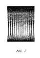
- FIG. 7is a scanning electron micrograph of a trench formed in accordance with embodiments of the invention.
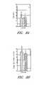
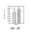
- FIGS. 8A-8Eare charts showing properties of etches according to embodiments of the invention and according to the prior art.
- Embodiments of the inventionprovide etch chemistries which enable passivation of the walls of an opening etched in a dielectric material, in combination with high profile control and high profile uniformity.
- the etch chemistriesinclude a silicon species and a halide species and also preferably include a carbon species and an oxygen species. At least one, and preferably, each of these species may be plasma excited species.
- the plasma excited speciesare derived or generated from silicon, carbon, and/or oxygen compounds.
- the silicon compoundcan be represented as Si x M y H z , where “Si” is silicon, “M” is one or more halogens (e.g., fluorine, bromine and/or chlorine), “H” is hydrogen and x ⁇ 1, y ⁇ 0 and z ⁇ 0 (preferably, y ⁇ 1).
- the etch chemistriesmay also include a carbon compound, which can be represented as C ⁇ M ⁇ H ⁇ , where “C” is carbon, “M” is one or more halogens, “H” is hydrogen, and ⁇ 1, ⁇ 0 and ⁇ 0 (preferably, ⁇ 1).
- the etch chemistriesmay include an oxygen compound (e.g., molecular oxygen (O 2 ), hydrogen peroxide (H 2 O 2 ) or water (H 2 O)).
- an oxygen compounde.g., molecular oxygen (O 2 ), hydrogen peroxide (H 2 O 2 ) or water (H 2 O)
- O 2molecular oxygen
- H 2 O 2hydrogen peroxide
- H 2 Owater
- compounds formed of silicon, carbon and halogen atomsare contemplated.
- the etch chemistriesadvantageously enable plasma etching of dielectric materials, such as an interlevel dielectric or silicon-containing dielectric materials, to form high aspect ratio openings.
- the silicon in the silicon compoundcan passivate the sidewalls of an opening forming a silicon layer on the sidewalls.
- the silicon layeris advantageously more resistant to etchants than, e.g., silicon-free polymer layers which may form using conventional fluorocarbon chemistries. This resistance to the etchants reduces bowing of the sidewalls relative to use of fluorocarbons alone.
- the silicon compoundadvantageously enables the degree of passivation and etching to be tailored, by appropriate selection of halogen constituents for the silicon compound and/or the carbon compound (when a carbon compound is included in the etch chemistry).
- etch chemistries according to the disclosed embodimentshave advantageously been found to offer higher selectivity than many conventional etch chemistries.
- the silicon passivating layercan dissipate charges which can build up during a plasma etch and which can repel plasma excited species from the surfaces defining an opening. By minimizing the charge build up, the etch rate can be increased, since more plasma excited species are allowed to reach the surfaces of the opening (e.g., via or trench) in the dielectric material.
- a patterned masking layer 120overlies a layer 130 of a dielectric or insulating material which will be etched, as discussed below.
- the masking layer 120includes a pattern of openings 110 .
- the patterned masking layer 120is a carbon-containing hard mask layer, preferably an amorphous carbon layer, e.g., a transparent amorphous carbon layer which is highly transparent to light. Deposition techniques for forming a highly transparent carbon can be found in A. Helmbold, D. Meissner, Thin Solid Films, 283 (1996) 196-203, the entire disclosure of which is incorporated herein by reference.
- the pattern of openings 110may be formed after a pattern transfer from one or more overlying layers, such as a photoresist layer and one or more intervening hardmask layers.
- the photoresistcan be exposed to radiation through a reticle and then developed to form a desired pattern which is transferred to the masking layer 120 .
- the masking layer 120is photoresist itself.
- the masking layer 120may be formed of a silicon-containing material, e.g., silicon or silicon nitride, that can be selectively etched and selected against relative to the dielectric material of the layer 130 .
- the layer 130comprises a dielectric material, which may be silicon-containing.
- the layer 130can be a form of silicon oxide and is preferably an interlevel dielectric (ILD) layer.
- the layer 130is formed of a silicon oxide, e.g., undoped silicon oxide such as silicon dioxide, fluorinated silicon oxide (FSG), silicate glasses such as borophosphate silicate glass (BPSG) and phosphate silicate glass (PSG), doped or undoped thermally grown silicon oxide, doped or undoped TEOS deposited silicon oxide, etc.
- a silicon oxidee.g., undoped silicon oxide such as silicon dioxide, fluorinated silicon oxide (FSG), silicate glasses such as borophosphate silicate glass (BPSG) and phosphate silicate glass (PSG), doped or undoped thermally grown silicon oxide, doped or undoped TEOS deposited silicon oxide, etc.
- plasma-excited speciesrefers to radicals, ions or other excited species generated via application of energy to a gas.
- Plasma-excited speciesmay be generated using a direct plasma generator (i.e., “in situ” or “direct” plasma generation) inside a reaction chamber containing a substrate or using a remote plasma generator (i.e., “ex situ” or “remote” plasma generation). The plasma-excited species may be generated in situ.
- Plasma-excited speciesmay include, without limitation, halide radicals and ions.
- plasma-excited speciese.g., F +
- plasma-excited speciesare preferably directed to the surface of a material to by etched, preferably via application of an electric field, to provide a directional or anisotropic etch.
- the plasma speciesare generated from an etch chemistry including a silicon compound and, more preferably, a silicon and halogen compound.
- the silicon compoundcan be represented generally by Si x M y H z , where “Si” is silicon; “M” is one or more halogens such as fluorine, bromine, chlorine or iodine; “H” is hydrogen and x ⁇ 1, y ⁇ 0 and z ⁇ 0. More preferably, the silicon compound includes a halogen to aid in etching of the layer 130 , so that y ⁇ 1.
- the silicon compoundis SiF 4 , which is a relatively aggressive etching compound.
- the etch chemistrycan also include combinations of different silicon compounds.
- the etch chemistryis preferably provided to a reaction chamber containing the partially fabricated integrated circuit 100 with the aid of an inert carrier gas (e.g., helium (He), argon (Ar) and neon (Ne)).
- an inert carrier gase.g., helium (He), argon (Ar) and neon (Ne)
- the etch chemistryalso includes a carbon compound.
- the carbon compoundcan be represented as C ⁇ M ⁇ H ⁇ , wherein “C” is carbon, “M” is one or more halogens, “H” is hydrogen, and ⁇ 1, ⁇ 0 and ⁇ 0. More preferably, at least one halogen is included to aid in etching of the layer 130 , so that ⁇ 1. Examples of carbon compounds include CF 4 and C 2 Br 6 . Combinations of different carbon containing compounds are also contemplated.
- the etch chemistrypreferably also includes the carbon compound.
- the carbon atomsadvantageously react with, e.g., oxygen atoms from silicon oxide, to form volatile carbon and oxygen compounds (e.g., CO and/or CO 2 ) which aid in removal of the oxygen atoms.
- the etch chemistrypreferably also includes an oxygen compound, which is preferably capable of combusting carbon.
- an oxygen compoundis molecular oxygen (O 2 ).
- the oxygen compoundcan be used to increase process latitude by removing carbon from the openings 150 by forming volatile compounds with the carbon (e.g., through a “combustion” reaction).
- carbon from the carbon compoundcan be utilized to remove oxygen of the dielectric layer 130 from the openings 150
- it may be desirable to deliver an excess of the carbon compound to the openings 150to, e.g., increase the aggressiveness of the etch.
- the use of the oxygen compoundadvantageously allows greater process latitude in the amount of the carbon compound delivered to the openings 150 since the oxygen compound can remove carbon that would otherwise accumulate in the openings 150 .
- the etch chemistryadvantageously deposits passivating films 160 on sidewalls 140 of the openings 150 , including on surfaces of the masking layer 120 .
- the silicon of the silicon compoundis believed to passivate the sidewalls 140 by depositing and polymerizing to form the passivating films 160 .
- carbon from the carbon compoundcan also deposit and polymerize to aid in formation of the passivating films 160 , particularly on surfaces of the masking layer 130 .
- the passivating films 160can be formed of a carbon-containing polymer (formed predominantly of carbon), while lower into the openings 150 , on the of the dielectric layer 130 , the passivating films 160 can be a silicon-containing polymer (formed predominantly of silicon), such as a silicone.
- silicon in the passivating films 160renders the film highly resistant to etching by etchants. Consequently, the passivating films 160 protects the sidewalls 140 from etching, thereby minimizing bowing. It will be understood that some etching of the passivating films 160 does occur, although this is considered minimal in comparison to conventional etches using fluorocarbons without the silicon compounds of the preferred embodiments. Rather than allowing the passivating films 160 to remain completely unetched, the etch chemistry is preferably selected to etch the passivating films 160 at a rate sufficient to prevent the passivating films 160 from growing to close off the openings 150 , while still allowing the passivating films 160 to protect the sidewalls 140 and to minimize bowing.
- the relatively high etch resistance of the passivating films 160allows a thinner passivating layer to be formed, thereby increasing the size of the opening at the neck region 162 .
- This relatively narrow passivating layer 160 and relatively wide neck opening 162advantageously contributes to improved profile control.
- the blocking of etchants by the neckcan be decreased, thereby reducing tapering of the openings 150 .
- straighter, more vertical sidewalls 140can be formed and the width of the openings 150 are more uniform through the height of the opening.
- the reduced taper of the openings 150may advantageously increase the etch rate by effectively decreasing the aspect ratio of the feature.
- the passivating films 160can advantageously increase the desired vertical etch rate. Due to the generation and use of plasma excited species during the etch, charges can build up on the sidewalls 140 . These charges can decrease the etch rate by repelling charged etchant species and undesirably reducing the number of such charged excited species which impinge on the bottom of the openings 150 .
- the silicon-containing layeris semiconductive, allowing for dissipation of charges and minimizing charge build-up. As a result, more charged etchant species can reach the bottom of the openings 150 , to etch material at that bottom, thereby increasing the etch rate.
- the bottom of the openings 150may charge positively, causing repulsion of positive ions of the etch chemistry. Reducing the positive charge at the bottom of the opening 150 , via the deposition of a conducting or semiconducting film, such as the silicon-containing film 160 , may increase the etch rate by reducing this repulsion.
- the relative degrees of passivation and etching strength of the etch chemistrycan be tailored by, among other parameters, appropriate selection of the halogen(s). It will be appreciated that the relative etching strengths of various halogens can be generalized as F>Cl>Br>I, ranging from most aggressive (F) to least aggressive (I). Combinations of halogens and hydrogens (e.g., SiF a Cl b Br c H d ) can be utilized to further tailor the relative degree of passivation and the etching strength.
- the ability to tailor the etch strength of the etch chemistry, including the silicon compoundadvantageously facilitates this balancing.
- the silicon compoundcan be, e.g., SiH 4 , allowing it to function principally as a passivating agent, while halide etchants are provide, e.g., as fluorocarbons.
- profile control over the openings 150can be achieved by appropriately selecting process parameters (e.g., plasma energy, plasma pulse duration, substrate temperature, reactor pressure and flow rates) and by selecting the compositions and relative ratios of the silicon, carbon and oxygen compounds in the etch chemistries delivered to the reaction chamber.
- process parameterse.g., plasma energy, plasma pulse duration, substrate temperature, reactor pressure and flow rates
- the aggressiveness of the etch chemistrycan be modified by selecting silicon and/or carbon compounds having halogens with greater or lesser etch strengths.
- only the silicon compoundis included in the etch chemistry (in which case, it contains halogen, but not carbon species), although, preferably, the carbon compound, and, more preferably, the carbon and the oxygen compounds are also included.
- the various compounds of the etch chemistrycan be flowed separately or intermittently into the reaction chamber.
- the carbon compound and the oxygen compoundcan be flowed continuously into the chamber, while the silicon compound is flowed intermittently into the chamber.
- the carbon compoundcan form a passivating film on the sidewalls of the mask opening.
- the overlying masking layer 120 and any passivating film on surfaces of the masking layer 120is also etched. As a result, the masking layer 120 may be worn thin and the neck and any bow formed by the etch may penetrate into the dielectric layer 130 .
- the carbon passivating filmmay also be etched, so that the neck formed by the carbon passivating film is formed progressively lower in the opening 150 .
- the neckmay move from the sidewalls of the mask opening to the sidewalls of the dielectric layer 130 .
- This lowered neckmay leave parts of the dielectric layer 130 above the neck unprotected from etchant.
- the silicon compoundcan be added to the etch chemistry.
- the silicon compoundmay deposit on the masking layer 120 , to increase the height of the mask and counteract thinning of the masking layer 120 .
- the flow of the silicon compoundcan be stopped for a time.
- the silicon compoundcan subsequently be added again before thinning of the masking layer 120 and etching of the passivating film again progresses to undesirable levels.
- the silicon-containing passivating agentcan be cyclically flowed in temporally-separated pulses while the carbon-containing ethants are either continuously flowed or alternated with the silicon-containing passivating agent.
- the masking layer 120can be removed and the openings 150 can be subjected to a post-etch cleaning process to form cleaned openings 150 a .
- the masking layer 120can be subjected to an etch or other process suitable for removing material which forms that layer.
- an ashing processcan be used to remove photoresist.
- the passivating films 160can be removed by various processes, including an ashing process using fluorine-containing gas, e.g., CF 4 in combination with O 2 and N 2 .
- fluorine-containing gase.g., CF 4 in combination with O 2 and N 2 .
- silicon from the etch chemistrymay form difficult to remove silicon compounds on the sidewalls 140 ( FIG. 4 ).
- a bias stripperrather a microwave stripper conventionally used for stripping processes, may be applied to remove the silicon compounds
- the etchcan be performed such that an opening extending completely through the layer 130 is formed.
- an underlying layer 170acts as an etch stop; the etch is selective to the underlying layer 170 relative to the material forming the layer 130 .
- openings 150 bare formed extending completely through the layer 130 , thereby exposing the underlying layer 170 .
- the openings 150 bcan be filled with material to form various features, such as conductive contacts in cases when the layer 170 includes a conductive feature, such as an interconnect.
- the etched layer 130can be used as a mask to transfer a pattern defined by the openings 150 b to the underlying layer 170 .
- the openings 150 bcan also be filled with material to form various electrical devices, such as transistors or capacitors.
- the openings 150 bcan be used to form a polysilicon plug for contact to container-shaped capacitors, which can also be formed in openings 150 b.
- the openings 150 a ( FIG. 5 ) or 150 b ( FIG. 6 )can have an aspect ratio (depth-to-width at the top of the openings) of about 15:1 or more, about 20:1 or, more preferably, about 30:1 or more, or about 40:1 or more.
- the openings 150 a or 150 bcan also be advantageously narrow, with widths of 100 nm or less, and as little as about 80 nm or less, or about 65 nm.
- the openings 150 a or 150 bmay be highly uniform through their depth, having variations in widths of less than about 10 nm RMS (within 3 sigma).
- the disclosed embodimentsadvantageously allow improvements, over conventional etches, in etch rates, in etch selectivity, in uniformity of features formed and in the aspect ratio of the openings which can be formed. In these categories, improvements of 15% and, more preferably, 25% are possible.
- these embodimentsallow etch rates of about 50-60 ⁇ /min. or more and selectivity of about 4:1 or more (for, e.g., the ratio of the etch rate for a silicon oxide layer and the etch rate for amorphous carbon layer) in forming the holes 150 a , 150 b ( FIGS. 5 and 6 ).
- the openings which are formedhave more uniform, nearly vertical sidewalls.
- the openings 150 a , 150 b having material, or dividers, 132 between the openings and that the amount of bowing of the sidewalls 140can be characterized with reference to the dividers 132 .
- the ratio of a top width 134 (the width of the dividers 132 at the top of the openings 150 a ) to a bow width 136 (the width of the dividers 132 at their narrowest point)may be less than or equal to about 1.4:1, less than or equal to about 1.3:1 or even less than or equal to about 1.2:1. In some embodiments, the ratio of the top width 134 to the bow width 136 is about 1.15:1.
- the degree of bowingis advantageously low.
- the dividers 132can function as insulating separation between conductors to be formed in the openings 150 a , 150 b .
- performing conventional etches using the same etch rate and having the same selectivitymay result in a ratio of top width 134 to bow width 136 which is about 25-30% larger than that resulting from some embodiments of the invention.
- a silicon oxide dielectric layerwas etched through an amorphous carbon masking layer to form trenches.
- the etchwas performed in a dual frequency capacitively coupled reactor, commercially available from Tokyo Electron Limited of Tokyo, Japan.
- the etch chemistryincluded SiF 4 , C 4 F 8 , and O 2 , provided to the reaction chamber with an argon carrier gas.
- the SiF 4was provided to the reaction chamber at a flow rate of about 18 standard cubic centimeters per minute (sccm), the C 4 F 8 was flowed at about 35 sccm, and the O 2 was flowed at 13 sccm.
- the substrate temperaturewas about 50° C. and the reaction chamber pressure was about 35 mTorr. 1500 W of power at 60 MHz was coupled to the top electrode and 2750 W of power at 2 MHz was coupled to the bottom electrode.
- the resultant trencheshad an aspect ratio of about 25:1 and a width of about 90 nm at their tops.
- the trencheshave exceptionally uniform and straight sidewalls.
- the etchwas found to give various improvements over a baseline etch utilizing an etch chemistry consisting of C 4 F 8 and O 2 with an Ar carrier gas.
- the selectivity of the etch for the silicon oxide relative to the amorphous carbon hard maskwas increased ( FIG. 8A ), while still achieving a high etch rate ( FIG. 8B ).
- the bow CDthe width of the un-etched dielectric material between trenches), or the bow width, was increased, indicating that bowing has decreased ( FIG. 8C ).
- the difference between the neck and the bow dimensionswas advantageously low, indicating that the walls of the trenches were exceptionally straight ( FIG. 8D ).
- the depth of the occurrence of any bowingwas lower that the baseline chemistry ( FIG. 8E ).
- thisfacilitates control over the degree of bowing and the profile of the etched opening.
- the etch chemistrycan be changed during the course of the etch so that any bowing is distributed more evenly over the height of the opening.
- the etch chemistrycan be varied from a chemistry which gives a relatively shallow bow depth (e.g., the baseline chemistry) to one which gives a relatively deep bow depth (SiF 4 ).
- a relatively shallow bow depthe.g., the baseline chemistry
- SiF 4relatively deep bow depth
- a methodfor forming an integrated circuit.
- the methodcomprises providing an interlevel dielectric (ILD) layer with an overlying masking layer in a reaction chamber.
- the masking layerhas openings exposing parts of the ILD layer.
- Plasma excited speciesare generated from a gas comprising a silicon compound.
- the ILD layeris etched by contacting the exposed parts of the ILD layer with the plasma excited species.
- a method for semiconductor processingcomprises etching a layer of a silicon-containing dielectric by contacting exposed portions of the silicon-containing dielectric layer with a chemistry comprising a halogen compound and a silicon compound. At least one of the compounds is in a plasma-excited state.
- a method for forming high aspect ratio features in an interlevel dielectric (ILD) layer over a semiconductor substratecomprises providing a masking layer over the ILD layer.
- the masking layerhas one or more openings partially exposing the dielectric layer. Exposed portions of the ILD layer are selectively etched relative to the masking layer using an etching chemistry.
- the etching chemistrycomprises a silicon species, a halide species, a carbon species and an oxygen species.
- a partially fabricated integrated circuit having an interlevel dielectric (ILD) layeris provided.
- the partially fabricated integrated circuitcomprises a plurality of features formed in the ILD layer.
- the featureshave sidewalls defined by openings in the ILD layer.
- a width at a top of each of the featuresdefines a top width and a minimum width of the features defines a bow width.
- a bow ratio of the top width to the bow widthis less than or equal to about 1.4:1.
- the partially fabricated integrated circuitalso comprises a silicon polymer film on at least part of the sidewalls.
Landscapes
- Engineering & Computer Science (AREA)
- Chemical & Material Sciences (AREA)
- Computer Hardware Design (AREA)
- Physics & Mathematics (AREA)
- Condensed Matter Physics & Semiconductors (AREA)
- General Physics & Mathematics (AREA)
- Manufacturing & Machinery (AREA)
- Microelectronics & Electronic Packaging (AREA)
- Power Engineering (AREA)
- Inorganic Chemistry (AREA)
- General Chemical & Material Sciences (AREA)
- Chemical Kinetics & Catalysis (AREA)
- Drying Of Semiconductors (AREA)
- Internal Circuitry In Semiconductor Integrated Circuit Devices (AREA)
- Electrodes Of Semiconductors (AREA)
Abstract
Description
Claims (16)
Priority Applications (9)
| Application Number | Priority Date | Filing Date | Title |
|---|---|---|---|
| US11/515,435US7517804B2 (en) | 2006-08-31 | 2006-08-31 | Selective etch chemistries for forming high aspect ratio features and associated structures |
| PCT/US2007/018398WO2008027240A2 (en) | 2006-08-31 | 2007-08-20 | Selective etch chemistries for forming high aspect ratio features and associated structures |
| CN2007800288924ACN101501824B (en) | 2006-08-31 | 2007-08-20 | Selective etch chemistries for forming high aspect ratio features and associated structures |
| KR1020097006586AKR101377866B1 (en) | 2006-08-31 | 2007-08-20 | Selective etch chemistries for forming high aspect ratio features and associated structures |
| JP2009526632AJP5273482B2 (en) | 2006-08-31 | 2007-08-20 | Method for semiconductor processing |
| EP07837078AEP2057669A2 (en) | 2006-08-31 | 2007-08-20 | Selective etch chemistries for forming high aspect ratio features and associated structures |
| TW096132268ATWI380362B (en) | 2006-08-31 | 2007-08-30 | Selective etch chemistries for forming high aspect ratio features and associated structures |
| US12/393,893US8088691B2 (en) | 2006-08-31 | 2009-02-26 | Selective etch chemistries for forming high aspect ratio features and associated structures |
| US13/305,603US20120068366A1 (en) | 2006-08-31 | 2011-11-28 | Selective etch chemistries for forming high aspect ratio features and associated structures |
Applications Claiming Priority (1)
| Application Number | Priority Date | Filing Date | Title |
|---|---|---|---|
| US11/515,435US7517804B2 (en) | 2006-08-31 | 2006-08-31 | Selective etch chemistries for forming high aspect ratio features and associated structures |
Related Child Applications (1)
| Application Number | Title | Priority Date | Filing Date |
|---|---|---|---|
| US12/393,893ContinuationUS8088691B2 (en) | 2006-08-31 | 2009-02-26 | Selective etch chemistries for forming high aspect ratio features and associated structures |
Publications (2)
| Publication Number | Publication Date |
|---|---|
| US20080057724A1 US20080057724A1 (en) | 2008-03-06 |
| US7517804B2true US7517804B2 (en) | 2009-04-14 |
Family
ID=39092870
Family Applications (3)
| Application Number | Title | Priority Date | Filing Date |
|---|---|---|---|
| US11/515,435Expired - Fee RelatedUS7517804B2 (en) | 2006-08-31 | 2006-08-31 | Selective etch chemistries for forming high aspect ratio features and associated structures |
| US12/393,893Active2027-06-16US8088691B2 (en) | 2006-08-31 | 2009-02-26 | Selective etch chemistries for forming high aspect ratio features and associated structures |
| US13/305,603AbandonedUS20120068366A1 (en) | 2006-08-31 | 2011-11-28 | Selective etch chemistries for forming high aspect ratio features and associated structures |
Family Applications After (2)
| Application Number | Title | Priority Date | Filing Date |
|---|---|---|---|
| US12/393,893Active2027-06-16US8088691B2 (en) | 2006-08-31 | 2009-02-26 | Selective etch chemistries for forming high aspect ratio features and associated structures |
| US13/305,603AbandonedUS20120068366A1 (en) | 2006-08-31 | 2011-11-28 | Selective etch chemistries for forming high aspect ratio features and associated structures |
Country Status (7)
| Country | Link |
|---|---|
| US (3) | US7517804B2 (en) |
| EP (1) | EP2057669A2 (en) |
| JP (1) | JP5273482B2 (en) |
| KR (1) | KR101377866B1 (en) |
| CN (1) | CN101501824B (en) |
| TW (1) | TWI380362B (en) |
| WO (1) | WO2008027240A2 (en) |
Cited By (9)
| Publication number | Priority date | Publication date | Assignee | Title |
|---|---|---|---|---|
| US20090159560A1 (en)* | 2006-08-31 | 2009-06-25 | Micron Technology, Inc. | Selective etch chemistries for forming high aspect ratio features and associated structures |
| US20100297849A1 (en)* | 2009-05-22 | 2010-11-25 | Masatoshi Miyake | Plasma etching method for etching an object |
| US20110059617A1 (en)* | 2009-09-10 | 2011-03-10 | Matheson Tri-Gas, Inc. | High aspect ratio silicon oxide etch |
| US20120083128A1 (en)* | 2010-10-05 | 2012-04-05 | National Taiwan University Of Science And Technology | Method for etching high-aspect-ratio features |
| US20190088497A1 (en)* | 2013-05-15 | 2019-03-21 | Tokyo Electron Limited | Plasma etching method and plasma etching apparatus |
| US10276439B2 (en) | 2017-06-02 | 2019-04-30 | International Business Machines Corporation | Rapid oxide etch for manufacturing through dielectric via structures |
| US20190196322A1 (en)* | 2017-12-22 | 2019-06-27 | Taiwan Semiconductor Manufacturing Co., Ltd. | Lithography mask with a black border region and method of fabricating the same |
| US10861693B2 (en) | 2015-12-18 | 2020-12-08 | Applied Materials, Inc. | Cleaning method |
| US12266534B2 (en) | 2020-06-15 | 2025-04-01 | Tokyo Electron Limited | Forming a semiconductor device using a protective layer |
Families Citing this family (45)
| Publication number | Priority date | Publication date | Assignee | Title |
|---|---|---|---|---|
| JP4507120B2 (en)* | 2005-11-11 | 2010-07-21 | エルピーダメモリ株式会社 | Manufacturing method of semiconductor integrated circuit device |
| US7608195B2 (en)* | 2006-02-21 | 2009-10-27 | Micron Technology, Inc. | High aspect ratio contacts |
| KR100849190B1 (en)* | 2007-03-19 | 2008-07-30 | 주식회사 하이닉스반도체 | Method of forming fine pattern of semiconductor device |
| US20090117745A1 (en)* | 2007-11-02 | 2009-05-07 | Li Siyi | Methods for selectively etching a barrier layer in dual damascene applications |
| US20100330805A1 (en)* | 2007-11-02 | 2010-12-30 | Kenny Linh Doan | Methods for forming high aspect ratio features on a substrate |
| JP4972594B2 (en)* | 2008-03-26 | 2012-07-11 | 東京エレクトロン株式会社 | Etching method and semiconductor device manufacturing method |
| US8226840B2 (en) | 2008-05-02 | 2012-07-24 | Micron Technology, Inc. | Methods of removing silicon dioxide |
| US7863180B2 (en)* | 2008-05-06 | 2011-01-04 | International Business Machines Corporation | Through substrate via including variable sidewall profile |
| JP5599355B2 (en)* | 2011-03-31 | 2014-10-01 | 富士フイルム株式会社 | Mold manufacturing method |
| US9653327B2 (en)* | 2011-05-12 | 2017-05-16 | Applied Materials, Inc. | Methods of removing a material layer from a substrate using water vapor treatment |
| KR101342038B1 (en)* | 2011-08-10 | 2013-12-16 | 에스케이하이닉스 주식회사 | Semiconductor device and method for fabricating the same |
| US8598040B2 (en)* | 2011-09-06 | 2013-12-03 | Lam Research Corporation | ETCH process for 3D flash structures |
| JP6001940B2 (en)* | 2012-07-11 | 2016-10-05 | 東京エレクトロン株式会社 | Pattern forming method and substrate processing system |
| US9132436B2 (en) | 2012-09-21 | 2015-09-15 | Applied Materials, Inc. | Chemical control features in wafer process equipment |
| US9165785B2 (en)* | 2013-03-29 | 2015-10-20 | Tokyo Electron Limited | Reducing bowing bias in etching an oxide layer |
| JP2015185770A (en)* | 2014-03-25 | 2015-10-22 | 株式会社東芝 | Manufacturing method of semiconductor device |
| US9640385B2 (en)* | 2015-02-16 | 2017-05-02 | Applied Materials, Inc. | Gate electrode material residual removal process |
| US9741593B2 (en) | 2015-08-06 | 2017-08-22 | Applied Materials, Inc. | Thermal management systems and methods for wafer processing systems |
| US10504700B2 (en) | 2015-08-27 | 2019-12-10 | Applied Materials, Inc. | Plasma etching systems and methods with secondary plasma injection |
| US9984858B2 (en)* | 2015-09-04 | 2018-05-29 | Lam Research Corporation | ALE smoothness: in and outside semiconductor industry |
| US9934984B2 (en)* | 2015-09-09 | 2018-04-03 | International Business Machines Corporation | Hydrofluorocarbon gas-assisted plasma etch for interconnect fabrication |
| US10504754B2 (en) | 2016-05-19 | 2019-12-10 | Applied Materials, Inc. | Systems and methods for improved semiconductor etching and component protection |
| US9865484B1 (en) | 2016-06-29 | 2018-01-09 | Applied Materials, Inc. | Selective etch using material modification and RF pulsing |
| US10658194B2 (en)* | 2016-08-23 | 2020-05-19 | Lam Research Corporation | Silicon-based deposition for semiconductor processing |
| US10037890B2 (en)* | 2016-10-11 | 2018-07-31 | Lam Research Corporation | Method for selectively etching with reduced aspect ratio dependence |
| US10546756B2 (en)* | 2016-11-29 | 2020-01-28 | Lam Research Corporation | Method for generating vertical profiles in organic layer etches |
| US10607850B2 (en) | 2016-12-30 | 2020-03-31 | American Air Liquide, Inc. | Iodine-containing compounds for etching semiconductor structures |
| JP7176860B6 (en) | 2017-05-17 | 2022-12-16 | アプライド マテリアルズ インコーポレイテッド | Semiconductor processing chamber to improve precursor flow |
| US11276590B2 (en) | 2017-05-17 | 2022-03-15 | Applied Materials, Inc. | Multi-zone semiconductor substrate supports |
| US11276559B2 (en) | 2017-05-17 | 2022-03-15 | Applied Materials, Inc. | Semiconductor processing chamber for multiple precursor flow |
| US11328909B2 (en) | 2017-12-22 | 2022-05-10 | Applied Materials, Inc. | Chamber conditioning and removal processes |
| KR102691504B1 (en) | 2018-06-19 | 2024-08-01 | 어플라이드 머티어리얼스, 인코포레이티드 | Improved pulsed plasma deposition etch step coverage |
| US11437242B2 (en)* | 2018-11-27 | 2022-09-06 | Applied Materials, Inc. | Selective removal of silicon-containing materials |
| US11107695B2 (en) | 2018-12-21 | 2021-08-31 | Beijing E-town Semiconductor Technology Co., Ltd. | Surface smoothing of workpieces |
| US11232954B2 (en) | 2020-03-16 | 2022-01-25 | Tokyo Electron Limited | Sidewall protection layer formation for substrate processing |
| WO2021207286A1 (en)* | 2020-04-08 | 2021-10-14 | Lam Research Corporation | Selective etch using deposition of a metalloid or metal containing hardmask |
| TW202213517A (en)* | 2020-08-28 | 2022-04-01 | 日商東京威力科創股份有限公司 | Substrate processing method and plasma processing apparatus |
| US11195723B1 (en)* | 2020-12-11 | 2021-12-07 | Tokyo Electron Limited | Non-atomic layer deposition (ALD) method of forming sidewall passivation layer during high aspect ratio carbon layer etch |
| US12106971B2 (en)* | 2020-12-28 | 2024-10-01 | American Air Liquide, Inc. | High conductive passivation layers and method of forming the same during high aspect ratio plasma etching |
| JP2024543922A (en)* | 2021-12-01 | 2024-11-26 | ラム リサーチ コーポレーション | Selective Etching of Semimetals or Metals Using Fluorocarbon-Based Depositions |
| CN118541781A (en)* | 2022-01-11 | 2024-08-23 | 朗姆研究公司 | Carbon mask deposition |
| KR20250004021A (en)* | 2022-05-05 | 2025-01-07 | 램 리써치 코포레이션 | Organic chloride etching with passivation and profile control |
| US20240105499A1 (en)* | 2022-09-28 | 2024-03-28 | Applied Materials, Inc. | Molecular layer deposition carbon masks for direct selective deposition of silicon-containing materials |
| WO2024091864A1 (en)* | 2022-10-24 | 2024-05-02 | Lam Research Corporation | Controllable carbon pecvd film deposition |
| WO2025117301A1 (en)* | 2023-11-27 | 2025-06-05 | Lam Research Corporation | SELECTIVE ETCH OF STACK USING A HYDROGEN CONTAINING COMPONENT AND AT LEAST ONE OF SeF6, AND IF7 AND TeF6 |
Citations (83)
| Publication number | Priority date | Publication date | Assignee | Title |
|---|---|---|---|---|
| US4234362A (en) | 1978-11-03 | 1980-11-18 | International Business Machines Corporation | Method for forming an insulator between layers of conductive material |
| US4419809A (en) | 1981-12-30 | 1983-12-13 | International Business Machines Corporation | Fabrication process of sub-micrometer channel length MOSFETs |
| US4432132A (en) | 1981-12-07 | 1984-02-21 | Bell Telephone Laboratories, Incorporated | Formation of sidewall oxide layers by reactive oxygen ion etching to define submicron features |
| US4502914A (en) | 1982-11-13 | 1985-03-05 | International Business Machines Corporation | Method of making structures with dimensions in the sub-micrometer range |
| US4508579A (en) | 1981-03-30 | 1985-04-02 | International Business Machines Corporation | Lateral device structures using self-aligned fabrication techniques |
| US4570325A (en) | 1983-12-16 | 1986-02-18 | Kabushiki Kaisha Toshiba | Manufacturing a field oxide region for a semiconductor device |
| US4615764A (en) | 1984-11-05 | 1986-10-07 | Allied Corporation | SF6/nitriding gas/oxidizer plasma etch system |
| US4648937A (en) | 1985-10-30 | 1987-03-10 | International Business Machines Corporation | Method of preventing asymmetric etching of lines in sub-micrometer range sidewall images transfer |
| EP0227303A2 (en) | 1985-11-25 | 1987-07-01 | Plessey Overseas Limited | Method of manufacturing semiconductor devices having side-wall isolation |
| US4687543A (en) | 1986-02-21 | 1987-08-18 | Tegal Corporation | Selective plasma etching during formation of integrated circuitry |
| US4776922A (en) | 1987-10-30 | 1988-10-11 | International Business Machines Corporation | Formation of variable-width sidewall structures |
| US4838991A (en) | 1987-10-30 | 1989-06-13 | International Business Machines Corporation | Process for defining organic sidewall structures |
| US4855017A (en)* | 1985-05-03 | 1989-08-08 | Texas Instruments Incorporated | Trench etch process for a single-wafer RIE dry etch reactor |
| US5013398A (en) | 1990-05-29 | 1991-05-07 | Micron Technology, Inc. | Anisotropic etch method for a sandwich structure |
| US5013400A (en) | 1990-01-30 | 1991-05-07 | General Signal Corporation | Dry etch process for forming champagne profiles, and dry etch apparatus |
| US5021121A (en) | 1990-02-16 | 1991-06-04 | Applied Materials, Inc. | Process for RIE etching silicon dioxide |
| US5022958A (en) | 1990-06-27 | 1991-06-11 | At&T Bell Laboratories | Method of etching for integrated circuits with planarized dielectric |
| EP0491408A2 (en) | 1990-11-20 | 1992-06-24 | Consorzio per la Ricerca sulla Microelettronica nel Mezzogiorno - CoRiMMe | Process for making planarized sub-micrometric trenches in integrated circuits |
| US5269879A (en) | 1991-10-16 | 1993-12-14 | Lam Research Corporation | Method of etching vias without sputtering of underlying electrically conductive layer |
| JPH05343370A (en) | 1992-06-10 | 1993-12-24 | Toshiba Corp | Method of forming fine pattern |
| US5328810A (en) | 1990-05-07 | 1994-07-12 | Micron Technology, Inc. | Method for reducing, by a factor or 2-N, the minimum masking pitch of a photolithographic process |
| US5445712A (en) | 1992-03-25 | 1995-08-29 | Sony Corporation | Dry etching method |
| JPH0855920A (en) | 1994-08-15 | 1996-02-27 | Toshiba Corp | Method for manufacturing semiconductor device |
| JPH0855908A (en) | 1994-08-17 | 1996-02-27 | Toshiba Corp | Semiconductor device |
| US5514885A (en) | 1986-10-09 | 1996-05-07 | Myrick; James J. | SOI methods and apparatus |
| US5529657A (en) | 1993-10-04 | 1996-06-25 | Tokyo Electron Limited | Plasma processing apparatus |
| US5595627A (en) | 1995-02-07 | 1997-01-21 | Tokyo Electron Limited | Plasma etching method |
| US5611888A (en) | 1995-09-29 | 1997-03-18 | Lam Research Corporation | Plasma etching of semiconductors |
| US5795830A (en) | 1995-06-06 | 1998-08-18 | International Business Machines Corporation | Reducing pitch with continuously adjustable line and space dimensions |
| US5820261A (en) | 1995-07-26 | 1998-10-13 | Applied Materials, Inc. | Method and apparatus for infrared pyrometer calibration in a rapid thermal processing system |
| US5882535A (en) | 1997-02-04 | 1999-03-16 | Micron Technology, Inc. | Method for forming a hole in a semiconductor device |
| US6004862A (en) | 1998-01-20 | 1999-12-21 | Advanced Micro Devices, Inc. | Core array and periphery isolation technique |
| US6042998A (en) | 1993-09-30 | 2000-03-28 | The University Of New Mexico | Method and apparatus for extending spatial frequencies in photolithography images |
| US6063688A (en) | 1997-09-29 | 2000-05-16 | Intel Corporation | Fabrication of deep submicron structures and quantum wire transistors using hard-mask transistor width definition |
| US6071789A (en) | 1998-11-10 | 2000-06-06 | Vanguard International Semiconductor Corporation | Method for simultaneously fabricating a DRAM capacitor and metal interconnections |
| US6090304A (en) | 1997-08-28 | 2000-07-18 | Lam Research Corporation | Methods for selective plasma etch |
| US6114250A (en) | 1998-08-17 | 2000-09-05 | Lam Research Corporation | Techniques for etching a low capacitance dielectric layer on a substrate |
| US6117786A (en) | 1998-05-05 | 2000-09-12 | Lam Research Corporation | Method for etching silicon dioxide using fluorocarbon gas chemistry |
| US6159862A (en) | 1997-12-27 | 2000-12-12 | Tokyo Electron Ltd. | Semiconductor processing method and system using C5 F8 |
| US6191043B1 (en) | 1999-04-20 | 2001-02-20 | Lam Research Corporation | Mechanism for etching a silicon layer in a plasma processing chamber to form deep openings |
| US6242165B1 (en) | 1998-08-28 | 2001-06-05 | Micron Technology, Inc. | Supercritical compositions for removal of organic material and methods of using same |
| US20010005631A1 (en) | 1999-12-14 | 2001-06-28 | Jin-Won Kim | Method for manufacturing an electrode of a capacitor |
| US6291334B1 (en) | 1997-12-19 | 2001-09-18 | Applied Materials, Inc. | Etch stop layer for dual damascene process |
| US6297554B1 (en) | 2000-03-10 | 2001-10-02 | United Microelectronics Corp. | Dual damascene interconnect structure with reduced parasitic capacitance |
| US20010031540A1 (en)* | 1999-07-12 | 2001-10-18 | Chartered Semiconductor Manufacturing Ltd. | Silicon nitride capped shallow trench isolation method for fabricating sub-micron devices with borderless contacts |
| US20020042198A1 (en) | 2000-09-20 | 2002-04-11 | Bjarni Bjarnason | Method in etching of a substrate |
| US6399514B1 (en)* | 1991-06-27 | 2002-06-04 | Applied Materials, Inc. | High temperature silicon surface providing high selectivity in an oxide etch process |
| US6403488B1 (en) | 1998-03-19 | 2002-06-11 | Cypress Semiconductor Corp. | Selective SAC etch process |
| US20020094641A1 (en) | 2001-01-18 | 2002-07-18 | Samsung Electronics Co., Ltd. | Method for fabricating floating gate |
| US6475867B1 (en) | 2001-04-02 | 2002-11-05 | Advanced Micro Devices, Inc. | Method of forming integrated circuit features by oxidation of titanium hard mask |
| WO2002099864A1 (en) | 2001-05-31 | 2002-12-12 | Infineon Technologies, Ag | Method for removing polysilane from a semiconductor without stripping |
| US20030044722A1 (en) | 2001-08-28 | 2003-03-06 | Yi-Yu Hsu | Process for improving critical dimension uniformity |
| US6548396B2 (en) | 1998-07-23 | 2003-04-15 | Applied Materials, Inc. | Method of producing an interconnect structure for an integrated circuit |
| US6573030B1 (en) | 2000-02-17 | 2003-06-03 | Applied Materials, Inc. | Method for depositing an amorphous carbon layer |
| US6579808B2 (en) | 2001-10-15 | 2003-06-17 | Hynix Semiconductor Inc. | Method of fabricating a semiconductor device |
| US6635185B2 (en)* | 1997-12-31 | 2003-10-21 | Alliedsignal Inc. | Method of etching and cleaning using fluorinated carbonyl compounds |
| EP1357433A2 (en) | 2002-04-23 | 2003-10-29 | Hewlett-Packard Company | Method of fabricating sub-lithographic sized line and space patterns |
| US20030207207A1 (en) | 2002-05-03 | 2003-11-06 | Weimin Li | Method of fabricating a semiconductor multilevel interconnect structure |
| US20030209520A1 (en) | 2002-05-09 | 2003-11-13 | Applied Materials, Inc. | Methods for etching an organic anti-reflective coating |
| US20030232504A1 (en) | 2002-06-14 | 2003-12-18 | Aaron Eppler | Process for etching dielectric films with improved resist and/or etch profile characteristics |
| US20040000534A1 (en) | 2002-06-28 | 2004-01-01 | Infineon Technologies North America Corp. | Hardmask of amorphous carbon-hydrogen (a-C:H) layers with tunable etch resistivity |
| US6673684B1 (en) | 2002-07-31 | 2004-01-06 | Advanced Micro Devices, Inc. | Use of diamond as a hard mask material |
| US20040023475A1 (en) | 2002-07-31 | 2004-02-05 | Advanced Micro Devices, Inc. | Method for reducing pattern deformation and photoresist poisoning in semiconductor device fabrication |
| US20040035826A1 (en) | 2000-12-21 | 2004-02-26 | Kenji Adachi | Etching method for insulating film |
| US20040043623A1 (en) | 2002-06-20 | 2004-03-04 | Wei Liu | Method for fabricating a gate structure of a field effect transistor |
| US20040043475A1 (en) | 2000-10-03 | 2004-03-04 | Friedrich Proll | Exhaust gas purification system |
| US6709991B1 (en)* | 1997-05-23 | 2004-03-23 | Nec Corporation | Method of fabricating semiconductor device with capacitor |
| US6709807B2 (en) | 1999-12-02 | 2004-03-23 | Axcelis Technologies, Inc. | Process for reducing edge roughness in patterned photoresist |
| US6716758B1 (en) | 1999-08-25 | 2004-04-06 | Micron Technology, Inc. | Aspect ratio controlled etch selectivity using time modulated DC bias voltage |
| US6734107B2 (en) | 2002-06-12 | 2004-05-11 | Macronix International Co., Ltd. | Pitch reduction in semiconductor fabrication |
| US20040106257A1 (en) | 2002-04-12 | 2004-06-03 | Matsushita Electric Industrial Co., Ltd. | Method for fabricating semiconductor device |
| US6746961B2 (en) | 2001-06-19 | 2004-06-08 | Lam Research Corporation | Plasma etching of dielectric layer with etch profile control |
| US6773998B1 (en) | 2003-05-20 | 2004-08-10 | Advanced Micro Devices, Inc. | Modified film stack and patterning strategy for stress compensation and prevention of pattern distortion in amorphous carbon gate patterning |
| US6784108B1 (en)* | 2000-08-31 | 2004-08-31 | Micron Technology, Inc. | Gas pulsing for etch profile control |
| US20040198015A1 (en)* | 2001-07-23 | 2004-10-07 | Christian Drabe | Method of forming an isolation layer and method of manufacturing a trench capacitor |
| US20040259355A1 (en) | 2003-06-17 | 2004-12-23 | Zhiping Yin | Boron-doped amorphous carbon film for use as a hard etch mask during the formation of a semiconductor device |
| US20050009215A1 (en) | 2003-07-09 | 2005-01-13 | Fujitsu Limited | Semiconductor device manufacture method and etching system |
| US20050026431A1 (en) | 2003-07-30 | 2005-02-03 | Hitachi High-Technologies Corporation | LSI device etching method and apparatus thereof |
| WO2005010973A1 (en) | 2003-07-18 | 2005-02-03 | Forschungszentrum Jülich GmbH | Method for the self-adjusted reduction in size of structures |
| US20050099078A1 (en) | 1999-05-03 | 2005-05-12 | Serge Vanhaelemeersch | Method for removal of SiC |
| US20050127416A1 (en) | 2003-12-10 | 2005-06-16 | Headway Technologies, Inc. | MRAM cell with flat topography and controlled bit line to free layer distance and method of manufacture |
| US20050148144A1 (en)* | 2003-12-10 | 2005-07-07 | International Business Machines Corporation | Selective post-doping of gate structures by means of selective oxide growth |
| US20050164478A1 (en) | 2004-01-26 | 2005-07-28 | Taiwan Semiconductor Manufacturing Co. | Novel method of trimming technology |
Family Cites Families (46)
| Publication number | Priority date | Publication date | Assignee | Title |
|---|---|---|---|---|
| US31540A (en)* | 1861-02-26 | Improvement in binding attachments to harvesters | ||
| US5631A (en)* | 1848-06-13 | Pianoeobte | ||
| US44722A (en)* | 1864-10-18 | Improvement in pneumatic drills | ||
| US42198A (en)* | 1864-04-05 | Improved window blind and curtain fixture | ||
| US259355A (en)* | 1882-06-13 | Caleb b | ||
| US207207A (en)* | 1878-08-20 | Improvement in carving-machines | ||
| US198015A (en)* | 1877-12-11 | Improvement in railway air-brakes | ||
| US534A (en)* | 1837-12-26 | Improved steam-generator | ||
| US164478A (en)* | 1875-06-15 | Improvement in permanent flour of camphor | ||
| US26431A (en)* | 1859-12-13 | John s | ||
| US148144A (en)* | 1874-03-03 | Improvement in lamp-chimney holders | ||
| US232504A (en)* | 1880-09-21 | Geefoed | ||
| US23475A (en)* | 1859-04-05 | Improvement in metallic cotton-bands | ||
| US127416A (en)* | 1872-06-04 | Improvement in wringing-mops | ||
| US43623A (en)* | 1864-07-19 | Improved ox-shoe | ||
| US209520A (en)* | 1878-10-29 | Improvement in wire-holders for making fence-cables | ||
| US106257A (en)* | 1870-08-09 | Improvement in machines for soldering metallic vessels | ||
| US35826A (en)* | 1862-07-08 | Improvement in steam-engines | ||
| US9215A (en)* | 1852-08-24 | Bed for invalids | ||
| US53475A (en)* | 1866-03-27 | Improvement in bee-hives | ||
| US99078A (en)* | 1870-01-25 | Improvement in cartridges | ||
| US94641A (en)* | 1869-09-07 | Improvement in wind-wheels | ||
| DD280851A1 (en) | 1989-03-27 | 1990-07-18 | Dresden Forschzentr Mikroelek | METHOD OF MAKING TRENCH MEMORY CELLS |
| US5017403A (en)* | 1989-04-13 | 1991-05-21 | Massachusetts Institute Of Technology | Process for forming planarized films |
| JP3038950B2 (en)* | 1991-02-12 | 2000-05-08 | ソニー株式会社 | Dry etching method |
| KR100276093B1 (en)* | 1992-10-19 | 2000-12-15 | 히가시 데쓰로 | Plasma etching system |
| US5426070A (en)* | 1993-05-26 | 1995-06-20 | Cornell Research Foundation, Inc. | Microstructures and high temperature isolation process for fabrication thereof |
| US5798830A (en)* | 1993-06-17 | 1998-08-25 | Ultrapointe Corporation | Method of establishing thresholds for image comparison |
| JPH1197414A (en)* | 1997-09-25 | 1999-04-09 | Sony Corp | Plasma etching method for silicon-oxide based insulating film |
| JP3744680B2 (en)* | 1998-03-31 | 2006-02-15 | 富士通株式会社 | Power supply device and method for controlling power supply circuit |
| US6284149B1 (en)* | 1998-09-18 | 2001-09-04 | Applied Materials, Inc. | High-density plasma etching of carbon-based low-k materials in a integrated circuit |
| EP1055967B1 (en)* | 1999-05-25 | 2004-09-29 | FERRANIA S.p.A. | Silver halide color photographic light-sensitive elements having improved image quality |
| US6291331B1 (en)* | 1999-10-04 | 2001-09-18 | Taiwan Semiconductor Manufacturing Company | Re-deposition high compressive stress PECVD oxide film after IMD CMP process to solve more than 5 metal stack via process IMD crack issue |
| US20050022839A1 (en)* | 1999-10-20 | 2005-02-03 | Savas Stephen E. | Systems and methods for photoresist strip and residue treatment in integrated circuit manufacturing |
| JP2002110647A (en)* | 2000-09-29 | 2002-04-12 | Hitachi Ltd | Method for manufacturing semiconductor integrated circuit device |
| US7132363B2 (en)* | 2001-03-27 | 2006-11-07 | Advanced Micro Devices, Inc. | Stabilizing fluorine etching of low-k materials |
| US20040072081A1 (en)* | 2002-05-14 | 2004-04-15 | Coleman Thomas P. | Methods for etching photolithographic reticles |
| JP2004087738A (en)* | 2002-08-26 | 2004-03-18 | Tokyo Electron Ltd | Si etching method |
| US6756284B2 (en)* | 2002-09-18 | 2004-06-29 | Silicon Storage Technology, Inc. | Method for forming a sublithographic opening in a semiconductor process |
| US6916746B1 (en)* | 2003-04-09 | 2005-07-12 | Lam Research Corporation | Method for plasma etching using periodic modulation of gas chemistry |
| US7115993B2 (en)* | 2004-01-30 | 2006-10-03 | Tokyo Electron Limited | Structure comprising amorphous carbon film and method of forming thereof |
| JP2005229052A (en)* | 2004-02-16 | 2005-08-25 | Seiko Epson Corp | Manufacturing method of semiconductor device |
| US20060043066A1 (en)* | 2004-08-26 | 2006-03-02 | Kamp Thomas A | Processes for pre-tapering silicon or silicon-germanium prior to etching shallow trenches |
| DE102005020060B4 (en)* | 2005-04-29 | 2012-02-23 | Advanced Micro Devices, Inc. | A method of patterning a low-k dielectric using a hardmask |
| KR100780944B1 (en)* | 2005-10-12 | 2007-12-03 | 삼성전자주식회사 | Carbon-containing film etching method and manufacturing method of semiconductor device using same |
| US7517804B2 (en)* | 2006-08-31 | 2009-04-14 | Micron Technologies, Inc. | Selective etch chemistries for forming high aspect ratio features and associated structures |
- 2006
- 2006-08-31USUS11/515,435patent/US7517804B2/ennot_activeExpired - Fee Related
- 2007
- 2007-08-20JPJP2009526632Apatent/JP5273482B2/enactiveActive
- 2007-08-20KRKR1020097006586Apatent/KR101377866B1/enactiveActive
- 2007-08-20WOPCT/US2007/018398patent/WO2008027240A2/enactiveApplication Filing
- 2007-08-20EPEP07837078Apatent/EP2057669A2/ennot_activeWithdrawn
- 2007-08-20CNCN2007800288924Apatent/CN101501824B/enactiveActive
- 2007-08-30TWTW096132268Apatent/TWI380362B/ennot_activeIP Right Cessation
- 2009
- 2009-02-26USUS12/393,893patent/US8088691B2/enactiveActive
- 2011
- 2011-11-28USUS13/305,603patent/US20120068366A1/ennot_activeAbandoned
Patent Citations (83)
| Publication number | Priority date | Publication date | Assignee | Title |
|---|---|---|---|---|
| US4234362A (en) | 1978-11-03 | 1980-11-18 | International Business Machines Corporation | Method for forming an insulator between layers of conductive material |
| US4508579A (en) | 1981-03-30 | 1985-04-02 | International Business Machines Corporation | Lateral device structures using self-aligned fabrication techniques |
| US4432132A (en) | 1981-12-07 | 1984-02-21 | Bell Telephone Laboratories, Incorporated | Formation of sidewall oxide layers by reactive oxygen ion etching to define submicron features |
| US4419809A (en) | 1981-12-30 | 1983-12-13 | International Business Machines Corporation | Fabrication process of sub-micrometer channel length MOSFETs |
| US4502914A (en) | 1982-11-13 | 1985-03-05 | International Business Machines Corporation | Method of making structures with dimensions in the sub-micrometer range |
| US4570325A (en) | 1983-12-16 | 1986-02-18 | Kabushiki Kaisha Toshiba | Manufacturing a field oxide region for a semiconductor device |
| US4615764A (en) | 1984-11-05 | 1986-10-07 | Allied Corporation | SF6/nitriding gas/oxidizer plasma etch system |
| US4855017A (en)* | 1985-05-03 | 1989-08-08 | Texas Instruments Incorporated | Trench etch process for a single-wafer RIE dry etch reactor |
| US4648937A (en) | 1985-10-30 | 1987-03-10 | International Business Machines Corporation | Method of preventing asymmetric etching of lines in sub-micrometer range sidewall images transfer |
| EP0227303A2 (en) | 1985-11-25 | 1987-07-01 | Plessey Overseas Limited | Method of manufacturing semiconductor devices having side-wall isolation |
| US4687543A (en) | 1986-02-21 | 1987-08-18 | Tegal Corporation | Selective plasma etching during formation of integrated circuitry |
| US5514885A (en) | 1986-10-09 | 1996-05-07 | Myrick; James J. | SOI methods and apparatus |
| US4776922A (en) | 1987-10-30 | 1988-10-11 | International Business Machines Corporation | Formation of variable-width sidewall structures |
| US4838991A (en) | 1987-10-30 | 1989-06-13 | International Business Machines Corporation | Process for defining organic sidewall structures |
| US5013400A (en) | 1990-01-30 | 1991-05-07 | General Signal Corporation | Dry etch process for forming champagne profiles, and dry etch apparatus |
| US5021121A (en) | 1990-02-16 | 1991-06-04 | Applied Materials, Inc. | Process for RIE etching silicon dioxide |
| US5328810A (en) | 1990-05-07 | 1994-07-12 | Micron Technology, Inc. | Method for reducing, by a factor or 2-N, the minimum masking pitch of a photolithographic process |
| US5013398A (en) | 1990-05-29 | 1991-05-07 | Micron Technology, Inc. | Anisotropic etch method for a sandwich structure |
| US5022958A (en) | 1990-06-27 | 1991-06-11 | At&T Bell Laboratories | Method of etching for integrated circuits with planarized dielectric |
| EP0491408A2 (en) | 1990-11-20 | 1992-06-24 | Consorzio per la Ricerca sulla Microelettronica nel Mezzogiorno - CoRiMMe | Process for making planarized sub-micrometric trenches in integrated circuits |
| US6399514B1 (en)* | 1991-06-27 | 2002-06-04 | Applied Materials, Inc. | High temperature silicon surface providing high selectivity in an oxide etch process |
| US5269879A (en) | 1991-10-16 | 1993-12-14 | Lam Research Corporation | Method of etching vias without sputtering of underlying electrically conductive layer |
| US5445712A (en) | 1992-03-25 | 1995-08-29 | Sony Corporation | Dry etching method |
| JPH05343370A (en) | 1992-06-10 | 1993-12-24 | Toshiba Corp | Method of forming fine pattern |
| US6042998A (en) | 1993-09-30 | 2000-03-28 | The University Of New Mexico | Method and apparatus for extending spatial frequencies in photolithography images |
| US5529657A (en) | 1993-10-04 | 1996-06-25 | Tokyo Electron Limited | Plasma processing apparatus |
| JPH0855920A (en) | 1994-08-15 | 1996-02-27 | Toshiba Corp | Method for manufacturing semiconductor device |
| JPH0855908A (en) | 1994-08-17 | 1996-02-27 | Toshiba Corp | Semiconductor device |
| US5595627A (en) | 1995-02-07 | 1997-01-21 | Tokyo Electron Limited | Plasma etching method |
| US5795830A (en) | 1995-06-06 | 1998-08-18 | International Business Machines Corporation | Reducing pitch with continuously adjustable line and space dimensions |
| US5820261A (en) | 1995-07-26 | 1998-10-13 | Applied Materials, Inc. | Method and apparatus for infrared pyrometer calibration in a rapid thermal processing system |
| US5611888A (en) | 1995-09-29 | 1997-03-18 | Lam Research Corporation | Plasma etching of semiconductors |
| US5882535A (en) | 1997-02-04 | 1999-03-16 | Micron Technology, Inc. | Method for forming a hole in a semiconductor device |
| US6709991B1 (en)* | 1997-05-23 | 2004-03-23 | Nec Corporation | Method of fabricating semiconductor device with capacitor |
| US6090304A (en) | 1997-08-28 | 2000-07-18 | Lam Research Corporation | Methods for selective plasma etch |
| US6063688A (en) | 1997-09-29 | 2000-05-16 | Intel Corporation | Fabrication of deep submicron structures and quantum wire transistors using hard-mask transistor width definition |
| US6291334B1 (en) | 1997-12-19 | 2001-09-18 | Applied Materials, Inc. | Etch stop layer for dual damascene process |
| US6159862A (en) | 1997-12-27 | 2000-12-12 | Tokyo Electron Ltd. | Semiconductor processing method and system using C5 F8 |
| US6635185B2 (en)* | 1997-12-31 | 2003-10-21 | Alliedsignal Inc. | Method of etching and cleaning using fluorinated carbonyl compounds |
| US6004862A (en) | 1998-01-20 | 1999-12-21 | Advanced Micro Devices, Inc. | Core array and periphery isolation technique |
| US6403488B1 (en) | 1998-03-19 | 2002-06-11 | Cypress Semiconductor Corp. | Selective SAC etch process |
| US6117786A (en) | 1998-05-05 | 2000-09-12 | Lam Research Corporation | Method for etching silicon dioxide using fluorocarbon gas chemistry |
| US6548396B2 (en) | 1998-07-23 | 2003-04-15 | Applied Materials, Inc. | Method of producing an interconnect structure for an integrated circuit |
| US6114250A (en) | 1998-08-17 | 2000-09-05 | Lam Research Corporation | Techniques for etching a low capacitance dielectric layer on a substrate |
| US6242165B1 (en) | 1998-08-28 | 2001-06-05 | Micron Technology, Inc. | Supercritical compositions for removal of organic material and methods of using same |
| US6071789A (en) | 1998-11-10 | 2000-06-06 | Vanguard International Semiconductor Corporation | Method for simultaneously fabricating a DRAM capacitor and metal interconnections |
| US6191043B1 (en) | 1999-04-20 | 2001-02-20 | Lam Research Corporation | Mechanism for etching a silicon layer in a plasma processing chamber to form deep openings |
| US20050099078A1 (en) | 1999-05-03 | 2005-05-12 | Serge Vanhaelemeersch | Method for removal of SiC |
| US20010031540A1 (en)* | 1999-07-12 | 2001-10-18 | Chartered Semiconductor Manufacturing Ltd. | Silicon nitride capped shallow trench isolation method for fabricating sub-micron devices with borderless contacts |
| US6716758B1 (en) | 1999-08-25 | 2004-04-06 | Micron Technology, Inc. | Aspect ratio controlled etch selectivity using time modulated DC bias voltage |
| US6709807B2 (en) | 1999-12-02 | 2004-03-23 | Axcelis Technologies, Inc. | Process for reducing edge roughness in patterned photoresist |
| US20010005631A1 (en) | 1999-12-14 | 2001-06-28 | Jin-Won Kim | Method for manufacturing an electrode of a capacitor |
| US6573030B1 (en) | 2000-02-17 | 2003-06-03 | Applied Materials, Inc. | Method for depositing an amorphous carbon layer |
| US6297554B1 (en) | 2000-03-10 | 2001-10-02 | United Microelectronics Corp. | Dual damascene interconnect structure with reduced parasitic capacitance |
| US6784108B1 (en)* | 2000-08-31 | 2004-08-31 | Micron Technology, Inc. | Gas pulsing for etch profile control |
| US20020042198A1 (en) | 2000-09-20 | 2002-04-11 | Bjarni Bjarnason | Method in etching of a substrate |
| US20040043475A1 (en) | 2000-10-03 | 2004-03-04 | Friedrich Proll | Exhaust gas purification system |
| US20040035826A1 (en) | 2000-12-21 | 2004-02-26 | Kenji Adachi | Etching method for insulating film |
| US20020094641A1 (en) | 2001-01-18 | 2002-07-18 | Samsung Electronics Co., Ltd. | Method for fabricating floating gate |
| US6475867B1 (en) | 2001-04-02 | 2002-11-05 | Advanced Micro Devices, Inc. | Method of forming integrated circuit features by oxidation of titanium hard mask |
| WO2002099864A1 (en) | 2001-05-31 | 2002-12-12 | Infineon Technologies, Ag | Method for removing polysilane from a semiconductor without stripping |
| US6746961B2 (en) | 2001-06-19 | 2004-06-08 | Lam Research Corporation | Plasma etching of dielectric layer with etch profile control |
| US20040198015A1 (en)* | 2001-07-23 | 2004-10-07 | Christian Drabe | Method of forming an isolation layer and method of manufacturing a trench capacitor |
| US20030044722A1 (en) | 2001-08-28 | 2003-03-06 | Yi-Yu Hsu | Process for improving critical dimension uniformity |
| US6579808B2 (en) | 2001-10-15 | 2003-06-17 | Hynix Semiconductor Inc. | Method of fabricating a semiconductor device |
| US20040106257A1 (en) | 2002-04-12 | 2004-06-03 | Matsushita Electric Industrial Co., Ltd. | Method for fabricating semiconductor device |
| EP1357433A2 (en) | 2002-04-23 | 2003-10-29 | Hewlett-Packard Company | Method of fabricating sub-lithographic sized line and space patterns |
| US20030207207A1 (en) | 2002-05-03 | 2003-11-06 | Weimin Li | Method of fabricating a semiconductor multilevel interconnect structure |
| US20030209520A1 (en) | 2002-05-09 | 2003-11-13 | Applied Materials, Inc. | Methods for etching an organic anti-reflective coating |
| US6734107B2 (en) | 2002-06-12 | 2004-05-11 | Macronix International Co., Ltd. | Pitch reduction in semiconductor fabrication |
| US20030232504A1 (en) | 2002-06-14 | 2003-12-18 | Aaron Eppler | Process for etching dielectric films with improved resist and/or etch profile characteristics |
| US20040043623A1 (en) | 2002-06-20 | 2004-03-04 | Wei Liu | Method for fabricating a gate structure of a field effect transistor |
| US20040000534A1 (en) | 2002-06-28 | 2004-01-01 | Infineon Technologies North America Corp. | Hardmask of amorphous carbon-hydrogen (a-C:H) layers with tunable etch resistivity |
| US20040023475A1 (en) | 2002-07-31 | 2004-02-05 | Advanced Micro Devices, Inc. | Method for reducing pattern deformation and photoresist poisoning in semiconductor device fabrication |
| US6673684B1 (en) | 2002-07-31 | 2004-01-06 | Advanced Micro Devices, Inc. | Use of diamond as a hard mask material |
| US6773998B1 (en) | 2003-05-20 | 2004-08-10 | Advanced Micro Devices, Inc. | Modified film stack and patterning strategy for stress compensation and prevention of pattern distortion in amorphous carbon gate patterning |
| US20040259355A1 (en) | 2003-06-17 | 2004-12-23 | Zhiping Yin | Boron-doped amorphous carbon film for use as a hard etch mask during the formation of a semiconductor device |
| US20050009215A1 (en) | 2003-07-09 | 2005-01-13 | Fujitsu Limited | Semiconductor device manufacture method and etching system |
| WO2005010973A1 (en) | 2003-07-18 | 2005-02-03 | Forschungszentrum Jülich GmbH | Method for the self-adjusted reduction in size of structures |
| US20050026431A1 (en) | 2003-07-30 | 2005-02-03 | Hitachi High-Technologies Corporation | LSI device etching method and apparatus thereof |
| US20050127416A1 (en) | 2003-12-10 | 2005-06-16 | Headway Technologies, Inc. | MRAM cell with flat topography and controlled bit line to free layer distance and method of manufacture |
| US20050148144A1 (en)* | 2003-12-10 | 2005-07-07 | International Business Machines Corporation | Selective post-doping of gate structures by means of selective oxide growth |
| US20050164478A1 (en) | 2004-01-26 | 2005-07-28 | Taiwan Semiconductor Manufacturing Co. | Novel method of trimming technology |
Non-Patent Citations (19)
| Title |
|---|
| "Advanced lithography: probing the limits of lithography," http://www.tpd.tno.nl/smartsite93.html, 3 pages (Mar. 2004). |
| "TCP 9400DFM-Silicon Etch", Product Abstract; Available at http://www.lamrc.com/products-5.htm, (Jul. 2004); 1 page. |
| Bergeron et al., "Resolution Enhancement Techniques for the 90nm Technology Node and Beyond," Future Fab International, Issue 15, 4 pages (Jul. 11, 2003). |
| Bhave et al., "Developer-soluble Gap fill materials for patterning metal trenches in Via-first Dual Damascene process," preprint of Proceedings of SPIE: Advances in Resist Technology and Processing XXI, vol. 5376, John L. Sturtevant, editor, 2004, 8 pages. |
| Chung et al., "Nanoscale Multi-Line Patterning Using Sidewall Structure," Jpn., J. App. Phys. vol. 41 Pt. 1, no. 6B, pp. 4410-4414 (2002). |
| Chung et al., "Pattern multiplication method and the uniformity of nanoscale multiple lines*," J.Vac.Sci.Technol. B21(4), pp. 1491-1495 (Jul./Aug. 2003). |
| Ha et al., "Reaction mechanism of trilevel resist etching in O2/SO2 plasma: controlling factors for sidewall passivation," Vacuum, vol. 51, Issue 4, pp. 519-524, Abstract (Dec. 1998). |
| Helmbold, A. and Meissner, D., Thin Solid Films, 283, 196-203 (1996). |
| Higashi et al., "Identifying front-end challenges for 90nm design," Electronic Eng. Times Asia, 3 pages, (Sep. 1, 2003). |
| Joubert et al., "Nanometer scale linewidth control during etching of polysilicon in high-density plasmas," Microelectronic Engineering 69 (2003), pp. 350-357. |
| Lopata, E. and Countrywood, J., "The effect of excitation frequency on emission spectra of polymerization plasmas," J. Vac. Sci. Technol. A 6(5) pp. 2949-2952 (Sep./Oct. 1988). |
| Mancini et al., "S-FIL for sub-80nm contact hole patterning," Solid State Technology Magazine, vol. 47, Issue 2, 4 pages (Feb. 2004). |
| Naulleau et al., "Line-edge roughness transfer function an dits application to determining mask effects in EUV resist characterization," Applied Optics, vol. 42, No. 17, pp. 3390-3397 (Jun. 10, 2003). |
| Oehrlein et al., "Pattern transfer into low dielctic materials by high-density plasma etching," Solid State Tech., 8 pages (May 2000). |
| PCT Search Report; and the Written Opinion of the International Searching Authority; Application No. PCT/US2007/018398; mailed Jun. 3, 2008. |
| Peterson et al., "Approachese to reducing edge roughness and substrate poisoning of ESCAP photoresists," Semiconductor Fabtech, 8th Edition, pp. 183-188. |
| Samukawa et al., "Effects of Dischargae Frequency in Plasma Etching and Ultrahigh-Frequency Plasma Source for High-Performance Etching for Ultralage-Scale Integrated Circuits," Jpn. J. Appl. Phys. vol. 39, pp. 1583-1596, Part 1, No. 4A (Apr. 2000). |
| Samukawa, S. and Mukai, T., "Differences in radical generation due to chemical bonding of gas molecules in a high-density fluorocarbon plasma: Effects of the C-C bond in fluorocarbon gases," J. Vac. Sci. Technol. A 17(5), pp. 2463-2466 (Sep./Oct. 1999). |
| Samukawa, S. and Mukai, T., "New radical control method for high-performance dielectric etching with nonperfluorocompound gas chemistries in ultrahigh-frequency plasma," J. Vac. Sci. Technol. A 17(5), pp. 2551-2556 (Sep./Oct. 1999). |
Cited By (20)
| Publication number | Priority date | Publication date | Assignee | Title |
|---|---|---|---|---|
| US8088691B2 (en)* | 2006-08-31 | 2012-01-03 | Micron Technology, Inc. | Selective etch chemistries for forming high aspect ratio features and associated structures |
| US20090159560A1 (en)* | 2006-08-31 | 2009-06-25 | Micron Technology, Inc. | Selective etch chemistries for forming high aspect ratio features and associated structures |
| US20100297849A1 (en)* | 2009-05-22 | 2010-11-25 | Masatoshi Miyake | Plasma etching method for etching an object |
| US8623148B2 (en) | 2009-09-10 | 2014-01-07 | Matheson Tri-Gas, Inc. | NF3 chamber clean additive |
| US20110059617A1 (en)* | 2009-09-10 | 2011-03-10 | Matheson Tri-Gas, Inc. | High aspect ratio silicon oxide etch |
| US20110056515A1 (en)* | 2009-09-10 | 2011-03-10 | Matheson Tri-Gas, Inc. | Nf3 chamber clean additive |
| US20110073136A1 (en)* | 2009-09-10 | 2011-03-31 | Matheson Tri-Gas, Inc. | Removal of gallium and gallium containing materials |
| US20120083128A1 (en)* | 2010-10-05 | 2012-04-05 | National Taiwan University Of Science And Technology | Method for etching high-aspect-ratio features |
| US20190088497A1 (en)* | 2013-05-15 | 2019-03-21 | Tokyo Electron Limited | Plasma etching method and plasma etching apparatus |
| US11355352B2 (en) | 2013-05-15 | 2022-06-07 | Tokyo Electron Limited | Plasma etching method and plasma etching apparatus |
| US10707091B2 (en)* | 2013-05-15 | 2020-07-07 | Tokyo Electron Limited | Plasma etching method and plasma etching apparatus |
| US12062522B2 (en) | 2013-05-15 | 2024-08-13 | Tokyo Electron Limited | Plasma etching method and plasma etching apparatus |
| US10861693B2 (en) | 2015-12-18 | 2020-12-08 | Applied Materials, Inc. | Cleaning method |
| US10276439B2 (en) | 2017-06-02 | 2019-04-30 | International Business Machines Corporation | Rapid oxide etch for manufacturing through dielectric via structures |
| US20190196322A1 (en)* | 2017-12-22 | 2019-06-27 | Taiwan Semiconductor Manufacturing Co., Ltd. | Lithography mask with a black border region and method of fabricating the same |
| US11029593B2 (en) | 2017-12-22 | 2021-06-08 | Taiwan Semiconductor Manufacturing Co., Ltd. | Lithography mask with a black border regions and method of fabricating the same |
| US10866504B2 (en)* | 2017-12-22 | 2020-12-15 | Taiwan Semiconductor Manufacturing Co., Ltd. | Lithography mask with a black border region and method of fabricating the same |
| US11852966B2 (en) | 2017-12-22 | 2023-12-26 | Taiwan Semiconductor Manufacturing Co., Ltd. | Lithography mask with a black border regions and method of fabricating the same |
| TWI713114B (en)* | 2017-12-22 | 2020-12-11 | 台灣積體電路製造股份有限公司 | Lithography mask, method of fabricating lithography mask, and method of performing lithography process |
| US12266534B2 (en) | 2020-06-15 | 2025-04-01 | Tokyo Electron Limited | Forming a semiconductor device using a protective layer |
Also Published As
| Publication number | Publication date |
|---|---|
| CN101501824B (en) | 2012-02-01 |
| US20120068366A1 (en) | 2012-03-22 |
| EP2057669A2 (en) | 2009-05-13 |
| CN101501824A (en) | 2009-08-05 |
| US8088691B2 (en) | 2012-01-03 |
| WO2008027240A2 (en) | 2008-03-06 |
| KR20090058005A (en) | 2009-06-08 |
| US20080057724A1 (en) | 2008-03-06 |
| US20090159560A1 (en) | 2009-06-25 |
| TWI380362B (en) | 2012-12-21 |
| JP2010503207A (en) | 2010-01-28 |
| JP5273482B2 (en) | 2013-08-28 |
| TW200823993A (en) | 2008-06-01 |
| WO2008027240A3 (en) | 2008-05-15 |
| KR101377866B1 (en) | 2014-03-24 |
Similar Documents
| Publication | Publication Date | Title |
|---|---|---|
| US7517804B2 (en) | Selective etch chemistries for forming high aspect ratio features and associated structures | |
| JP2010503207A5 (en) | ||
| KR101158205B1 (en) | Method of etching a high aspect ratio contact | |
| JP3659933B2 (en) | Method for etching high aspect ratio openings | |
| US6183655B1 (en) | Tunable process for selectively etching oxide using fluoropropylene and a hydrofluorocarbon | |
| US6583065B1 (en) | Sidewall polymer forming gas additives for etching processes | |
| US6306772B1 (en) | Deep trench bottle-shaped etching using Cl2 gas | |
| US6613689B2 (en) | Magnetically enhanced plasma oxide etch using hexafluorobutadiene | |
| US6380095B1 (en) | Silicon trench etch using silicon-containing precursors to reduce or avoid mask erosion | |
| US7547635B2 (en) | Process for etching dielectric films with improved resist and/or etch profile characteristics | |
| US7241665B2 (en) | Shallow trench isolation | |
| KR100255405B1 (en) | Dry etching method | |
| JP7630530B2 (en) | Isotropic Silicon Nitride Removal | |
| US7029992B2 (en) | Low oxygen content photoresist stripping process for low dielectric constant materials | |
| US6372634B1 (en) | Plasma etch chemistry and method of improving etch control | |
| KR101276043B1 (en) | An etch back process using nitrous oxide | |
| KR100777925B1 (en) | How to Form Metal Wiring | |
| KR20010030088A (en) | Process for etching an insulating layer and forming a semiconductor devices | |
| JP6163820B2 (en) | Etching method |
Legal Events
| Date | Code | Title | Description |
|---|---|---|---|
| AS | Assignment | Owner name:MICRON TECHNOLOGIES, INC., IDAHO Free format text:ASSIGNMENT OF ASSIGNORS INTEREST;ASSIGNORS:KIEHLBAUCH, MARK;TAYLOR, TED;REEL/FRAME:018267/0819 Effective date:20060831 | |
| FEPP | Fee payment procedure | Free format text:PAYOR NUMBER ASSIGNED (ORIGINAL EVENT CODE: ASPN); ENTITY STATUS OF PATENT OWNER: LARGE ENTITY | |
| AS | Assignment | Owner name:MICRON TECHNOLOGY, INC.,IDAHO Free format text:ASSIGNMENT OF ASSIGNORS INTEREST;ASSIGNORS:KIEHLBAUCH, MARK;TAYLOR, TED;REEL/FRAME:024242/0383 Effective date:20100407 | |
| FEPP | Fee payment procedure | Free format text:PAYER NUMBER DE-ASSIGNED (ORIGINAL EVENT CODE: RMPN); ENTITY STATUS OF PATENT OWNER: LARGE ENTITY Free format text:PAYOR NUMBER ASSIGNED (ORIGINAL EVENT CODE: ASPN); ENTITY STATUS OF PATENT OWNER: LARGE ENTITY | |
| FPAY | Fee payment | Year of fee payment:4 | |
| AS | Assignment | Owner name:U.S. BANK NATIONAL ASSOCIATION, AS COLLATERAL AGENT, CALIFORNIA Free format text:SECURITY INTEREST;ASSIGNOR:MICRON TECHNOLOGY, INC.;REEL/FRAME:038669/0001 Effective date:20160426 Owner name:U.S. BANK NATIONAL ASSOCIATION, AS COLLATERAL AGEN Free format text:SECURITY INTEREST;ASSIGNOR:MICRON TECHNOLOGY, INC.;REEL/FRAME:038669/0001 Effective date:20160426 | |
| AS | Assignment | Owner name:MORGAN STANLEY SENIOR FUNDING, INC., AS COLLATERAL AGENT, MARYLAND Free format text:PATENT SECURITY AGREEMENT;ASSIGNOR:MICRON TECHNOLOGY, INC.;REEL/FRAME:038954/0001 Effective date:20160426 Owner name:MORGAN STANLEY SENIOR FUNDING, INC., AS COLLATERAL Free format text:PATENT SECURITY AGREEMENT;ASSIGNOR:MICRON TECHNOLOGY, INC.;REEL/FRAME:038954/0001 Effective date:20160426 | |
| REMI | Maintenance fee reminder mailed | ||
| LAPS | Lapse for failure to pay maintenance fees | ||
| STCH | Information on status: patent discontinuation | Free format text:PATENT EXPIRED DUE TO NONPAYMENT OF MAINTENANCE FEES UNDER 37 CFR 1.362 | |
| FP | Lapsed due to failure to pay maintenance fee | Effective date:20170414 | |
| AS | Assignment | Owner name:U.S. BANK NATIONAL ASSOCIATION, AS COLLATERAL AGENT, CALIFORNIA Free format text:CORRECTIVE ASSIGNMENT TO CORRECT THE REPLACE ERRONEOUSLY FILED PATENT #7358718 WITH THE CORRECT PATENT #7358178 PREVIOUSLY RECORDED ON REEL 038669 FRAME 0001. ASSIGNOR(S) HEREBY CONFIRMS THE SECURITY INTEREST;ASSIGNOR:MICRON TECHNOLOGY, INC.;REEL/FRAME:043079/0001 Effective date:20160426 Owner name:U.S. BANK NATIONAL ASSOCIATION, AS COLLATERAL AGEN Free format text:CORRECTIVE ASSIGNMENT TO CORRECT THE REPLACE ERRONEOUSLY FILED PATENT #7358718 WITH THE CORRECT PATENT #7358178 PREVIOUSLY RECORDED ON REEL 038669 FRAME 0001. ASSIGNOR(S) HEREBY CONFIRMS THE SECURITY INTEREST;ASSIGNOR:MICRON TECHNOLOGY, INC.;REEL/FRAME:043079/0001 Effective date:20160426 | |
| AS | Assignment | Owner name:MICRON TECHNOLOGY, INC., IDAHO Free format text:RELEASE BY SECURED PARTY;ASSIGNOR:U.S. BANK NATIONAL ASSOCIATION, AS COLLATERAL AGENT;REEL/FRAME:047243/0001 Effective date:20180629 | |
| AS | Assignment | Owner name:MICRON TECHNOLOGY, INC., IDAHO Free format text:RELEASE BY SECURED PARTY;ASSIGNOR:MORGAN STANLEY SENIOR FUNDING, INC., AS COLLATERAL AGENT;REEL/FRAME:050937/0001 Effective date:20190731 |