US7517775B2 - Methods of selective deposition of heavily doped epitaxial SiGe - Google Patents
Methods of selective deposition of heavily doped epitaxial SiGeDownload PDFInfo
- Publication number
- US7517775B2 US7517775B2US11/420,906US42090606AUS7517775B2US 7517775 B2US7517775 B2US 7517775B2US 42090606 AUS42090606 AUS 42090606AUS 7517775 B2US7517775 B2US 7517775B2
- Authority
- US
- United States
- Prior art keywords
- silicon
- substrate
- containing film
- gas
- range
- Prior art date
- Legal status (The legal status is an assumption and is not a legal conclusion. Google has not performed a legal analysis and makes no representation as to the accuracy of the status listed.)
- Expired - Lifetime, expires
Links
- 238000000034methodMethods0.000titleclaimsabstractdescription111
- 230000008021depositionEffects0.000titleclaimsabstractdescription49
- 229910000577Silicon-germaniumInorganic materials0.000titleabstractdescription48
- 239000000758substrateSubstances0.000claimsabstractdescription84
- 230000008569processEffects0.000claimsabstractdescription79
- XUIMIQQOPSSXEZ-UHFFFAOYSA-NSiliconChemical compound[Si]XUIMIQQOPSSXEZ-UHFFFAOYSA-N0.000claimsabstractdescription59
- 229910052710siliconInorganic materials0.000claimsabstractdescription59
- 239000010703siliconSubstances0.000claimsabstractdescription59
- BLRPTPMANUNPDV-UHFFFAOYSA-NSilaneChemical compound[SiH4]BLRPTPMANUNPDV-UHFFFAOYSA-N0.000claimsabstractdescription49
- 239000012159carrier gasSubstances0.000claimsabstractdescription39
- 239000002019doping agentSubstances0.000claimsabstractdescription37
- 239000007789gasSubstances0.000claimsabstractdescription32
- 238000010438heat treatmentMethods0.000claimsabstractdescription9
- 229910000077silaneInorganic materials0.000claimsdescription39
- VEXZGXHMUGYJMC-UHFFFAOYSA-NHydrochloric acidChemical compoundClVEXZGXHMUGYJMC-UHFFFAOYSA-N0.000claimsdescription36
- 150000001875compoundsChemical class0.000claimsdescription32
- OKTJSMMVPCPJKN-UHFFFAOYSA-NCarbonChemical compound[C]OKTJSMMVPCPJKN-UHFFFAOYSA-N0.000claimsdescription22
- 229910052799carbonInorganic materials0.000claimsdescription22
- MROCJMGDEKINLD-UHFFFAOYSA-NdichlorosilaneChemical compoundCl[SiH2]ClMROCJMGDEKINLD-UHFFFAOYSA-N0.000claimsdescription18
- 229910052796boronInorganic materials0.000claimsdescription16
- ZOXJGFHDIHLPTG-UHFFFAOYSA-NBoronChemical compound[B]ZOXJGFHDIHLPTG-UHFFFAOYSA-N0.000claimsdescription15
- 229910020254Cl2SiH2Inorganic materials0.000claimsdescription8
- 239000003989dielectric materialSubstances0.000claimsdescription6
- 229910052698phosphorusInorganic materials0.000claimsdescription5
- OAICVXFJPJFONN-UHFFFAOYSA-NPhosphorusChemical compound[P]OAICVXFJPJFONN-UHFFFAOYSA-N0.000claimsdescription4
- 239000011574phosphorusSubstances0.000claimsdescription4
- 229910052785arsenicInorganic materials0.000claimsdescription3
- RQNWIZPPADIBDY-UHFFFAOYSA-Narsenic atomChemical compound[As]RQNWIZPPADIBDY-UHFFFAOYSA-N0.000claimsdescription2
- LALRXNPLTWZJIJ-UHFFFAOYSA-NtriethylboraneChemical compoundCCB(CC)CCLALRXNPLTWZJIJ-UHFFFAOYSA-N0.000claimsdescription2
- 238000000151depositionMethods0.000abstractdescription63
- 229910052732germaniumInorganic materials0.000abstractdescription34
- GNPVGFCGXDBREM-UHFFFAOYSA-Ngermanium atomChemical compound[Ge]GNPVGFCGXDBREM-UHFFFAOYSA-N0.000abstractdescription34
- LEVVHYCKPQWKOP-UHFFFAOYSA-N[Si].[Ge]Chemical compound[Si].[Ge]LEVVHYCKPQWKOP-UHFFFAOYSA-N0.000abstractdescription17
- 238000004519manufacturing processMethods0.000abstractdescription5
- 239000011261inert gasSubstances0.000abstractdescription2
- 150000003377silicon compoundsChemical class0.000description82
- IXCSERBJSXMMFS-UHFFFAOYSA-Nhydrogen chlorideSubstancesCl.ClIXCSERBJSXMMFS-UHFFFAOYSA-N0.000description32
- 229910000041hydrogen chlorideInorganic materials0.000description32
- 125000004429atomChemical group0.000description19
- 229910003811SiGeCInorganic materials0.000description13
- 125000002496methyl groupChemical group[H]C([H])([H])*0.000description13
- 239000004065semiconductorSubstances0.000description13
- 125000001495ethyl groupChemical group[H]C([H])([H])C([H])([H])*0.000description11
- 229910052739hydrogenInorganic materials0.000description11
- 239000001257hydrogenSubstances0.000description11
- 239000012686silicon precursorSubstances0.000description11
- 235000012431wafersNutrition0.000description11
- VYPSYNLAJGMNEJ-UHFFFAOYSA-NSilicium dioxideChemical compoundO=[Si]=OVYPSYNLAJGMNEJ-UHFFFAOYSA-N0.000description9
- 238000005229chemical vapour depositionMethods0.000description9
- QUZPNFFHZPRKJD-UHFFFAOYSA-NgermaneChemical compound[GeH4]QUZPNFFHZPRKJD-UHFFFAOYSA-N0.000description9
- 229910052986germanium hydrideInorganic materials0.000description9
- 229910000078germaneInorganic materials0.000description8
- 239000000463materialSubstances0.000description8
- 229910052581Si3N4Inorganic materials0.000description7
- 238000000137annealingMethods0.000description7
- 239000003153chemical reaction reagentSubstances0.000description7
- 238000000407epitaxyMethods0.000description7
- 239000000203mixtureSubstances0.000description7
- 229910021420polycrystalline siliconInorganic materials0.000description7
- UFHFLCQGNIYNRP-UHFFFAOYSA-NHydrogenChemical compound[H][H]UFHFLCQGNIYNRP-UHFFFAOYSA-N0.000description6
- 229910052751metalInorganic materials0.000description6
- 239000002184metalSubstances0.000description6
- XYFCBTPGUUZFHI-UHFFFAOYSA-NPhosphineChemical compoundPXYFCBTPGUUZFHI-UHFFFAOYSA-N0.000description5
- 238000000231atomic layer depositionMethods0.000description5
- 125000000484butyl groupChemical group[H]C([*])([H])C([H])([H])C([H])([H])C([H])([H])[H]0.000description5
- 150000002431hydrogenChemical class0.000description5
- UIUXUFNYAYAMOE-UHFFFAOYSA-NmethylsilaneChemical compound[SiH3]CUIUXUFNYAYAMOE-UHFFFAOYSA-N0.000description5
- 125000001436propyl groupChemical group[H]C([*])([H])C([H])([H])C([H])([H])[H]0.000description5
- UORVGPXVDQYIDP-UHFFFAOYSA-NboraneChemical classBUORVGPXVDQYIDP-UHFFFAOYSA-N0.000description4
- 229910021419crystalline siliconInorganic materials0.000description4
- 238000005530etchingMethods0.000description4
- 239000005001laminate filmSubstances0.000description4
- 229920005591polysiliconPolymers0.000description4
- 229910021332silicideInorganic materials0.000description4
- FVBUAEGBCNSCDD-UHFFFAOYSA-Nsilicide(4-)Chemical compound[Si-4]FVBUAEGBCNSCDD-UHFFFAOYSA-N0.000description4
- 239000000377silicon dioxideSubstances0.000description4
- AXQKVSDUCKWEKE-UHFFFAOYSA-N[C].[Ge].[Si]Chemical compound[C].[Ge].[Si]AXQKVSDUCKWEKE-UHFFFAOYSA-N0.000description3
- 229910021417amorphous siliconInorganic materials0.000description3
- RBFQJDQYXXHULB-UHFFFAOYSA-NarsaneChemical compound[AsH3]RBFQJDQYXXHULB-UHFFFAOYSA-N0.000description3
- 238000003877atomic layer epitaxyMethods0.000description3
- 229910000085boraneInorganic materials0.000description3
- 229910017052cobaltInorganic materials0.000description3
- 239000010941cobaltSubstances0.000description3
- GUTLYIVDDKVIGB-UHFFFAOYSA-Ncobalt atomChemical compound[Co]GUTLYIVDDKVIGB-UHFFFAOYSA-N0.000description3
- 229910052681coesiteInorganic materials0.000description3
- 229910052906cristobaliteInorganic materials0.000description3
- 238000002955isolationMethods0.000description3
- PXHVJJICTQNCMI-UHFFFAOYSA-NnickelSubstances[Ni]PXHVJJICTQNCMI-UHFFFAOYSA-N0.000description3
- 239000002243precursorSubstances0.000description3
- 229910052682stishoviteInorganic materials0.000description3
- 229910052905tridymiteInorganic materials0.000description3
- YWWDBCBWQNCYNR-UHFFFAOYSA-NtrimethylphosphineChemical compoundCP(C)CYWWDBCBWQNCYNR-UHFFFAOYSA-N0.000description3
- HSFWRNGVRCDJHI-UHFFFAOYSA-NAcetyleneChemical compoundC#CHSFWRNGVRCDJHI-UHFFFAOYSA-N0.000description2
- -1Organosilane compoundsChemical class0.000description2
- ATUOYWHBWRKTHZ-UHFFFAOYSA-NPropaneChemical compoundCCCATUOYWHBWRKTHZ-UHFFFAOYSA-N0.000description2
- QQONPFPTGQHPMA-UHFFFAOYSA-NPropeneChemical compoundCC=CQQONPFPTGQHPMA-UHFFFAOYSA-N0.000description2
- 229910003828SiH3Inorganic materials0.000description2
- 238000013459approachMethods0.000description2
- 238000000277atomic layer chemical vapour depositionMethods0.000description2
- 230000015572biosynthetic processEffects0.000description2
- KDKYADYSIPSCCQ-UHFFFAOYSA-Nbut-1-yneChemical compoundCCC#CKDKYADYSIPSCCQ-UHFFFAOYSA-N0.000description2
- 238000006243chemical reactionMethods0.000description2
- 238000005137deposition processMethods0.000description2
- YOTZYFSGUCFUKA-UHFFFAOYSA-NdimethylphosphineChemical compoundCPCYOTZYFSGUCFUKA-UHFFFAOYSA-N0.000description2
- WHYHZFHCWGGCOP-UHFFFAOYSA-NgermylChemical compound[GeH3]WHYHZFHCWGGCOP-UHFFFAOYSA-N0.000description2
- NEXSMEBSBIABKL-UHFFFAOYSA-NhexamethyldisilaneChemical compoundC[Si](C)(C)[Si](C)(C)CNEXSMEBSBIABKL-UHFFFAOYSA-N0.000description2
- 238000002513implantationMethods0.000description2
- 238000011065in-situ storageMethods0.000description2
- 239000012212insulatorSubstances0.000description2
- 238000001182laser chemical vapour depositionMethods0.000description2
- VNWKTOKETHGBQD-UHFFFAOYSA-NmethaneChemical compoundCVNWKTOKETHGBQD-UHFFFAOYSA-N0.000description2
- 229910003465moissaniteInorganic materials0.000description2
- 229910052759nickelInorganic materials0.000description2
- 150000004767nitridesChemical class0.000description2
- 150000001282organosilanesChemical class0.000description2
- 229910000073phosphorus hydrideInorganic materials0.000description2
- 238000000623plasma-assisted chemical vapour depositionMethods0.000description2
- 150000004756silanesChemical class0.000description2
- 229910010271silicon carbideInorganic materials0.000description2
- FDNAPBUWERUEDA-UHFFFAOYSA-Nsilicon tetrachlorideChemical compoundCl[Si](Cl)(Cl)ClFDNAPBUWERUEDA-UHFFFAOYSA-N0.000description2
- 239000002210silicon-based materialSubstances0.000description2
- OLRJXMHANKMLTD-UHFFFAOYSA-NsilylChemical compound[SiH3]OLRJXMHANKMLTD-UHFFFAOYSA-N0.000description2
- 125000006850spacer groupChemical group0.000description2
- VZGDMQKNWNREIO-UHFFFAOYSA-NtetrachloromethaneChemical compoundClC(Cl)(Cl)ClVZGDMQKNWNREIO-UHFFFAOYSA-N0.000description2
- LXEXBJXDGVGRAR-UHFFFAOYSA-Ntrichloro(trichlorosilyl)silaneChemical compoundCl[Si](Cl)(Cl)[Si](Cl)(Cl)ClLXEXBJXDGVGRAR-UHFFFAOYSA-N0.000description2
- WXRGABKACDFXMG-UHFFFAOYSA-NtrimethylboraneChemical compoundCB(C)CWXRGABKACDFXMG-UHFFFAOYSA-N0.000description2
- 238000000038ultrahigh vacuum chemical vapour depositionMethods0.000description2
- HNEJIUSZPOMSFT-UHFFFAOYSA-NC[GeH2][GeH3]Chemical compoundC[GeH2][GeH3]HNEJIUSZPOMSFT-UHFFFAOYSA-N0.000description1
- UFIKLRNUCHZRPW-UHFFFAOYSA-NC[GeH](C)[GeH3]Chemical compoundC[GeH](C)[GeH3]UFIKLRNUCHZRPW-UHFFFAOYSA-N0.000description1
- VGGSQFUCUMXWEO-UHFFFAOYSA-NEtheneChemical compoundC=CVGGSQFUCUMXWEO-UHFFFAOYSA-N0.000description1
- 239000005977EthyleneSubstances0.000description1
- YZCKVEUIGOORGS-UHFFFAOYSA-NHydrogen atomChemical compound[H]YZCKVEUIGOORGS-UHFFFAOYSA-N0.000description1
- CPELXLSAUQHCOX-UHFFFAOYSA-NHydrogen bromideChemical compoundBrCPELXLSAUQHCOX-UHFFFAOYSA-N0.000description1
- 229910007245Si2Cl6Inorganic materials0.000description1
- 229910007258Si2H4Inorganic materials0.000description1
- 229910003910SiCl4Inorganic materials0.000description1
- RTAQQCXQSZGOHL-UHFFFAOYSA-NTitaniumChemical compound[Ti]RTAQQCXQSZGOHL-UHFFFAOYSA-N0.000description1
- HMDDXIMCDZRSNE-UHFFFAOYSA-N[C].[Si]Chemical compound[C].[Si]HMDDXIMCDZRSNE-UHFFFAOYSA-N0.000description1
- 230000004913activationEffects0.000description1
- 150000001336alkenesChemical class0.000description1
- 150000001345alkine derivativesChemical class0.000description1
- 125000000217alkyl groupChemical group0.000description1
- 229910000070arsenic hydrideInorganic materials0.000description1
- 230000004888barrier functionEffects0.000description1
- 230000000295complement effectEffects0.000description1
- 238000011109contaminationMethods0.000description1
- 239000013078crystalSubstances0.000description1
- BUMGIEFFCMBQDG-UHFFFAOYSA-NdichlorosiliconChemical compoundCl[Si]ClBUMGIEFFCMBQDG-UHFFFAOYSA-N0.000description1
- FAFYLCKQPJOORN-UHFFFAOYSA-NdiethylboraneChemical compoundCCBCCFAFYLCKQPJOORN-UHFFFAOYSA-N0.000description1
- VZZJVOCVAZHETD-UHFFFAOYSA-NdiethylphosphaneChemical compoundCCPCCVZZJVOCVAZHETD-UHFFFAOYSA-N0.000description1
- 238000009792diffusion processMethods0.000description1
- VXGHASBVNMHGDI-UHFFFAOYSA-NdigermaneChemical compound[Ge][Ge]VXGHASBVNMHGDI-UHFFFAOYSA-N0.000description1
- UCMVNBCLTOOHMN-UHFFFAOYSA-Ndimethyl(silyl)silaneChemical compoundC[SiH](C)[SiH3]UCMVNBCLTOOHMN-UHFFFAOYSA-N0.000description1
- GMLFPSKPTROTFV-UHFFFAOYSA-NdimethylboraneChemical compoundCBCGMLFPSKPTROTFV-UHFFFAOYSA-N0.000description1
- RUIGDFHKELAHJL-UHFFFAOYSA-NdimethylgermaneChemical compoundC[GeH2]CRUIGDFHKELAHJL-UHFFFAOYSA-N0.000description1
- UBHZUDXTHNMNLD-UHFFFAOYSA-NdimethylsilaneChemical compoundC[SiH2]CUBHZUDXTHNMNLD-UHFFFAOYSA-N0.000description1
- JZZIHCLFHIXETF-UHFFFAOYSA-NdimethylsiliconChemical compoundC[Si]CJZZIHCLFHIXETF-UHFFFAOYSA-N0.000description1
- PZPGRFITIJYNEJ-UHFFFAOYSA-NdisilaneChemical compound[SiH3][SiH3]PZPGRFITIJYNEJ-UHFFFAOYSA-N0.000description1
- 125000000047disilanyl groupChemical group[H][Si]([*])([H])[Si]([H])([H])[H]0.000description1
- 238000005516engineering processMethods0.000description1
- AIGRXSNSLVJMEA-FQEVSTJZSA-Nethoxy-(4-nitrophenoxy)-phenyl-sulfanylidene-$l^{5}-phosphaneChemical compoundO([P@@](=S)(OCC)C=1C=CC=CC=1)C1=CC=C([N+]([O-])=O)C=C1AIGRXSNSLVJMEA-FQEVSTJZSA-N0.000description1
- SHRMMCOTNQGWJS-UHFFFAOYSA-NethylgermaneChemical compoundCC[GeH3]SHRMMCOTNQGWJS-UHFFFAOYSA-N0.000description1
- KCWYOFZQRFCIIE-UHFFFAOYSA-NethylsilaneChemical compoundCC[SiH3]KCWYOFZQRFCIIE-UHFFFAOYSA-N0.000description1
- 230000005669field effectEffects0.000description1
- 238000004050hot filament vapor depositionMethods0.000description1
- 229910000042hydrogen bromideInorganic materials0.000description1
- 230000033444hydroxylationEffects0.000description1
- 238000005805hydroxylation reactionMethods0.000description1
- 238000010348incorporationMethods0.000description1
- 238000005468ion implantationMethods0.000description1
- 150000002500ionsChemical class0.000description1
- 229910044991metal oxideInorganic materials0.000description1
- 150000004706metal oxidesChemical class0.000description1
- 238000002488metal-organic chemical vapour depositionMethods0.000description1
- 150000002739metalsChemical class0.000description1
- IQCYANORSDPPDT-UHFFFAOYSA-Nmethyl(silyl)silaneChemical compoundC[SiH2][SiH3]IQCYANORSDPPDT-UHFFFAOYSA-N0.000description1
- FOTXTBSEOHNRCB-UHFFFAOYSA-NmethylgermaneChemical compound[GeH3]CFOTXTBSEOHNRCB-UHFFFAOYSA-N0.000description1
- 125000002524organometallic groupChemical group0.000description1
- 230000003647oxidationEffects0.000description1
- 238000007254oxidation reactionMethods0.000description1
- BPUBBGLMJRNUCC-UHFFFAOYSA-Noxygen(2-);tantalum(5+)Chemical compound[O-2].[O-2].[O-2].[O-2].[O-2].[Ta+5].[Ta+5]BPUBBGLMJRNUCC-UHFFFAOYSA-N0.000description1
- 230000037361pathwayEffects0.000description1
- 238000005498polishingMethods0.000description1
- 238000011165process developmentMethods0.000description1
- 239000001294propaneSubstances0.000description1
- 230000009467reductionEffects0.000description1
- 238000006722reduction reactionMethods0.000description1
- 235000012239silicon dioxideNutrition0.000description1
- 229910052814silicon oxideInorganic materials0.000description1
- 238000006467substitution reactionMethods0.000description1
- 229910001936tantalum oxideInorganic materials0.000description1
- 238000002230thermal chemical vapour depositionMethods0.000description1
- 229910052719titaniumInorganic materials0.000description1
- 239000010936titaniumSubstances0.000description1
- RXJKFRMDXUJTEX-UHFFFAOYSA-NtriethylphosphineChemical compoundCCP(CC)CCRXJKFRMDXUJTEX-UHFFFAOYSA-N0.000description1
- CKQULDKQRNJABT-UHFFFAOYSA-NtrimethylgermaniumChemical compoundC[Ge](C)C.C[Ge](C)CCKQULDKQRNJABT-UHFFFAOYSA-N0.000description1
- VEDJZFSRVVQBIL-UHFFFAOYSA-NtrisilaneChemical compound[SiH3][SiH2][SiH3]VEDJZFSRVVQBIL-UHFFFAOYSA-N0.000description1
- 229910052721tungstenInorganic materials0.000description1
Images


Classifications
- H—ELECTRICITY
- H01—ELECTRIC ELEMENTS
- H01L—SEMICONDUCTOR DEVICES NOT COVERED BY CLASS H10
- H01L21/00—Processes or apparatus adapted for the manufacture or treatment of semiconductor or solid state devices or of parts thereof
- H01L21/02—Manufacture or treatment of semiconductor devices or of parts thereof
- H01L21/04—Manufacture or treatment of semiconductor devices or of parts thereof the devices having potential barriers, e.g. a PN junction, depletion layer or carrier concentration layer
- H01L21/18—Manufacture or treatment of semiconductor devices or of parts thereof the devices having potential barriers, e.g. a PN junction, depletion layer or carrier concentration layer the devices having semiconductor bodies comprising elements of Group IV of the Periodic Table or AIIIBV compounds with or without impurities, e.g. doping materials
- H01L21/20—Deposition of semiconductor materials on a substrate, e.g. epitaxial growth solid phase epitaxy
- H—ELECTRICITY
- H01—ELECTRIC ELEMENTS
- H01L—SEMICONDUCTOR DEVICES NOT COVERED BY CLASS H10
- H01L21/00—Processes or apparatus adapted for the manufacture or treatment of semiconductor or solid state devices or of parts thereof
- H01L21/02—Manufacture or treatment of semiconductor devices or of parts thereof
- H01L21/02104—Forming layers
- H01L21/02365—Forming inorganic semiconducting materials on a substrate
- H01L21/02367—Substrates
- H01L21/0237—Materials
- H—ELECTRICITY
- H01—ELECTRIC ELEMENTS
- H01L—SEMICONDUCTOR DEVICES NOT COVERED BY CLASS H10
- H01L21/00—Processes or apparatus adapted for the manufacture or treatment of semiconductor or solid state devices or of parts thereof
- H01L21/02—Manufacture or treatment of semiconductor devices or of parts thereof
- H01L21/02104—Forming layers
- H01L21/02365—Forming inorganic semiconducting materials on a substrate
- H01L21/02518—Deposited layers
- H01L21/02521—Materials
- H01L21/02524—Group 14 semiconducting materials
- H01L21/02532—Silicon, silicon germanium, germanium
- H—ELECTRICITY
- H01—ELECTRIC ELEMENTS
- H01L—SEMICONDUCTOR DEVICES NOT COVERED BY CLASS H10
- H01L21/00—Processes or apparatus adapted for the manufacture or treatment of semiconductor or solid state devices or of parts thereof
- H01L21/02—Manufacture or treatment of semiconductor devices or of parts thereof
- H01L21/02104—Forming layers
- H01L21/02365—Forming inorganic semiconducting materials on a substrate
- H01L21/02518—Deposited layers
- H01L21/0257—Doping during depositing
- H01L21/02573—Conductivity type
- H01L21/02576—N-type
- H—ELECTRICITY
- H01—ELECTRIC ELEMENTS
- H01L—SEMICONDUCTOR DEVICES NOT COVERED BY CLASS H10
- H01L21/00—Processes or apparatus adapted for the manufacture or treatment of semiconductor or solid state devices or of parts thereof
- H01L21/02—Manufacture or treatment of semiconductor devices or of parts thereof
- H01L21/02104—Forming layers
- H01L21/02365—Forming inorganic semiconducting materials on a substrate
- H01L21/02518—Deposited layers
- H01L21/0257—Doping during depositing
- H01L21/02573—Conductivity type
- H01L21/02579—P-type
- H—ELECTRICITY
- H01—ELECTRIC ELEMENTS
- H01L—SEMICONDUCTOR DEVICES NOT COVERED BY CLASS H10
- H01L21/00—Processes or apparatus adapted for the manufacture or treatment of semiconductor or solid state devices or of parts thereof
- H01L21/02—Manufacture or treatment of semiconductor devices or of parts thereof
- H01L21/02104—Forming layers
- H01L21/02365—Forming inorganic semiconducting materials on a substrate
- H01L21/02612—Formation types
- H01L21/02617—Deposition types
- H01L21/0262—Reduction or decomposition of gaseous compounds, e.g. CVD
- H—ELECTRICITY
- H01—ELECTRIC ELEMENTS
- H01L—SEMICONDUCTOR DEVICES NOT COVERED BY CLASS H10
- H01L21/00—Processes or apparatus adapted for the manufacture or treatment of semiconductor or solid state devices or of parts thereof
- H01L21/02—Manufacture or treatment of semiconductor devices or of parts thereof
- H01L21/02104—Forming layers
- H01L21/02365—Forming inorganic semiconducting materials on a substrate
- H01L21/02612—Formation types
- H01L21/02617—Deposition types
- H01L21/02636—Selective deposition, e.g. simultaneous growth of mono- and non-monocrystalline semiconductor materials
- H—ELECTRICITY
- H10—SEMICONDUCTOR DEVICES; ELECTRIC SOLID-STATE DEVICES NOT OTHERWISE PROVIDED FOR
- H10D—INORGANIC ELECTRIC SEMICONDUCTOR DEVICES
- H10D30/00—Field-effect transistors [FET]
- H10D30/60—Insulated-gate field-effect transistors [IGFET]
- H10D30/791—Arrangements for exerting mechanical stress on the crystal lattice of the channel regions
- H10D30/797—Arrangements for exerting mechanical stress on the crystal lattice of the channel regions being in source or drain regions, e.g. SiGe source or drain
- H—ELECTRICITY
- H10—SEMICONDUCTOR DEVICES; ELECTRIC SOLID-STATE DEVICES NOT OTHERWISE PROVIDED FOR
- H10D—INORGANIC ELECTRIC SEMICONDUCTOR DEVICES
- H10D30/00—Field-effect transistors [FET]
- H10D30/60—Insulated-gate field-effect transistors [IGFET]
Definitions
- Selective Si epitaxial deposition and SiGe epitaxial depositionpermits growth of epilayers on Si moats with no growth on dielectric areas.
- Selective epitaxycan be used in semiconductor devices, such as within elevated source/drains, source/drain extensions, contact plugs, and base layer deposition of bipolar devices.
- a selective epitaxy processinvolves two reactions: deposition and etching. They occur simultaneously with relatively different reaction rates on Si and on dielectric surface.
- a selective process windowresults in deposition only on Si surfaces by changing the concentration of an etchant gas (e.g., HCl).
- an etchant gase.g., HCl
- the inventiongenerally provides a method of depositing a silicon germanium film on a substrate comprising placing the substrate within a process chamber and heating the substrate surface to a temperature in a range from about 500° C. to about 900° C. while maintaining a pressure in a range from about 0.1 Torr to about 200 Torr.
- a deposition gasis provided to the process chamber and includes SiH 4 , GeH 4 , HCl, a carrier gas and at least one dopant gas, such as diborane, arsine or phosphine.
- a doped silicon germanium filmis epitaxially grown on the substrate.
- the inventionprovides a process to epitaxially deposit silicon containing compounds during the manufacture of various device structures.
- the processutilizes the silicon precursor silane (SiH 4 ) during the deposition of silicon compounds.
- silicon precursorssuch as dichlorosilane, tetrachlorosilane or hexachlorodisilane
- processes of the present inventionteach the utilization of silane as a precursor.
- the use of silanehas been found to deposit silicon containing films more quickly than that of dichlorosilane.
- the use of silane during these processesprovides a higher degree of control for dopant concentrations within the film and increased deposition rate.
- the flow rate of the germanium sourceis from about 0.1 sccm to about 10 sccm.
- the flow rate of the etchantis from about 5 sccm to about 1,000 sccm.
- the process chamberis maintained with a pressure from about 0.1 Torr to about 200 Torr, preferably at about 15 Torr.
- the substrateis kept at a temperature in the range from about 500° C. to about 1,000° C., preferably from about 700° C. to about 900° C.
- the reagent mixtureis thermally driven to react and epitaxially deposit a silicon compound, namely a silicon germanium film.
- the HCletches any deposited amorphous SiGe compounds from dielectric features upon the surface of the substrate.
- boron containing dopantsinclude boranes and organoboranes.
- Boranesinclude borane, triborane, tetraborane and pentaborane
- Alkylboranesinclude trimethylborane ((CH 3 ) 3 B), dimethylborane ((CH 3 ) 2 BH), triethylborane ((CH 3 CH 2 ) 3 B) and diethylborane ((CH 3 CH 2 ) 2 BH).
- the reagent mixtureis thermally driven to react and epitaxially deposit a silicon compound, namely a silicon germanium carbon film.
- the HCletches any deposited amorphous or polycrystalline SiGeC compounds from dielectric features upon the surface of the substrate.
- the processis conducted to form the deposited SiGeC compound with a thickness in a range from about 100 ⁇ to about 3,000 ⁇ and at a deposition rate between about 50 ⁇ /min and about 600 ⁇ /min, preferably at about 150 ⁇ /min.
- the germanium concentrationis in the range from about 1 atomic percent to about 30 atomic percent of the SiGeC compound, preferably at about 20 atomic percent.
- the carbon concentrationis in the range from about 0.1 atomic percent to about 5 atomic percent, preferably at about 2 atomic percent of the SiGeC compound.
- silicon compoundsinclude a germanium concentration within the range from about 0 atomic percent to about 95 atomic percent. In another embodiment, a germanium concentration is within the range from about 1 atomic percent to about 30 atomic percent, preferably from about 15 atomic percent to about 25 atomic percent and more preferably at about 20 atomic percent. Silicon compounds also include a carbon concentration within the range from about 0 atomic percent to about 5 atomic percent. In other aspects, a carbon concentration is within the range from about 200 ppm to about 2 atomic percent.
- the silicon compound films of germanium and/or carbonare produced by various processes of the invention and can have consistent, sporadic or graded elemental concentrations.
- Graded silicon germanium filmsare disclosed in U.S. Patent Applications 20020174826 and 20020174827 assigned to Applied Materials, Inc., and are incorporated herein by reference in their entirety for the purpose of describing methods of depositing graded silicon compound films.
- silane and a germanium sourcee.g., GeH 4
- the ratio of silane and germanium sourcecan be varied in order to provide control of the elemental concentrations while growing graded films.
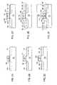
- FIG. 2Cillustrates several embodiments of the present invention, in which silicon compound layers 140 (epitaxial) and 142 (polycrystalline) are selectively deposited. Silicon compound layers 140 and 142 are deposited simultaneously without depositing on the off-set layer 134 . Silicon compound layers 140 and 142 are generally doped SiGe containing layers with a germanium concentration at about 1 atomic percent to about 30 atomic percent, preferably at about 20 atomic percent and a dopant (e.g., B, As or P) concentration from about 1 ⁇ 10 20 atoms/cm 3 to about 2.5 ⁇ 10 21 atoms/cm 3 , preferably at about 2 ⁇ 10 20 atoms/cm 3 .
- FIG. 2Dshows the nitride spacer 144 (e.g., Si 3 N 4 ) deposited to the off-set layer 134 .
Landscapes
- Engineering & Computer Science (AREA)
- Microelectronics & Electronic Packaging (AREA)
- Condensed Matter Physics & Semiconductors (AREA)
- General Physics & Mathematics (AREA)
- Manufacturing & Machinery (AREA)
- Computer Hardware Design (AREA)
- Physics & Mathematics (AREA)
- Power Engineering (AREA)
- Chemical & Material Sciences (AREA)
- Materials Engineering (AREA)
- Insulated Gate Type Field-Effect Transistor (AREA)
- Bipolar Transistors (AREA)
- Metal-Oxide And Bipolar Metal-Oxide Semiconductor Integrated Circuits (AREA)
- Thin Film Transistor (AREA)
- Chemical Vapour Deposition (AREA)
Abstract
Description
This application is a divisional application of U.S. patent application Ser. No. 10/683,937, filed Oct. 10, 2003 now U.S. Pat. No. 7,166,528, which is incorporated by reference herein.
1. Field of the Invention
Embodiments of the invention generally relate to the field of semiconductor manufacturing processes and devices, more particular, to methods of depositing silicon-containing films forming semiconductor devices.
2. Description of the Related Art
As smaller transistors are manufactured, ultra shallow source/drain junctions are becoming more challenging to produce. According to the International Technology Roadmap for Semiconductors (ITRS), junction depth is required to be less than 30 nm for sub-100 nm CMOS (complementary metal-oxide semiconductor) devices. Conventional doping by implantation and annealing is less effective as the junction depth approaches 10 nm. Doping by implantation requires a post-annealing process in order to activate dopants and post-annealing causes enhanced dopant diffusion into layers.
Recently, heavily-doped (about >1019atoms/cm3), selective SiGe epitaxy has become a useful material to deposit during formation of elevated source/drain and source/drain extension features. Source/drain extension features are manufactured by etching silicon to make a recessed source/drain feature and subsequently filling the etched surface with a selectively grown SiGe epilayer. Selective epitaxy permits near complete dopant activation with in-situ doping, so that the post annealing process is omitted. Therefore, junction depth can be defined accurately by silicon etching and selective epitaxy. On the other hand, the ultra shallow source/drain junction inevitably results in increased series resistance. Also, junction consumption during silicide formation increases the series resistance even further. In order to compensate for junction consumption, an elevated source/drain is epitaxially and selectively grown on the junction.
Selective Si epitaxial deposition and SiGe epitaxial deposition permits growth of epilayers on Si moats with no growth on dielectric areas. Selective epitaxy can be used in semiconductor devices, such as within elevated source/drains, source/drain extensions, contact plugs, and base layer deposition of bipolar devices. Generally, a selective epitaxy process involves two reactions: deposition and etching. They occur simultaneously with relatively different reaction rates on Si and on dielectric surface. A selective process window results in deposition only on Si surfaces by changing the concentration of an etchant gas (e.g., HCl). A popular process to perform selective, epitaxy deposition is to use dichlorosilane (SiH2Cl2) as a silicon source, germane (GeH4) as a germanium source, HCl as an etchant to provide selectivity during the deposition and hydrogen (H2) as a carrier gas.
Although SiGe epitaxial deposition is suitable for small dimensions, this approach does not readily prepare doped SiGe, since the dopants react with HCl. The process development of heavily boron doped (e.g., higher than 5×1019cm−3) selective SiGe epitaxy is a much more complicated task because boron doping makes the process window for selective deposition narrow. Generally, when more boron concentration (e.g., B2H6) is added to the flow, a higher HCl concentration is necessary to achieve selectivity due to the increase growth rate of deposited film(s) on any dielectric areas. This higher HCl flow rate proportionally reduces boron incorporation into the epilayers presumably because the B—Cl bond is stronger than Ge—Cl and Si—Cl bonds.
Therefore, there is a need to have a process for selectively and epitaxially depositing silicon and silicon compounds with an enriched dopant concentration. Furthermore, the process must maintain a high growth of the deposited material. Also, the process must have less dependency on germanium and boron concentrations in the silicon compound in relation to an etchant flow rate.
In one embodiment, the invention generally provides a method of depositing a silicon germanium film on a substrate comprising placing the substrate within a process chamber and heating the substrate surface to a temperature in a range from about 500° C. to about 900° C. while maintaining a pressure in a range from about 0.1 Torr to about 200 Torr. A deposition gas is provided to the process chamber and includes SiH4, GeH4, HCl, a carrier gas and at least one dopant gas, such as diborane, arsine or phosphine. A doped silicon germanium film is epitaxially grown on the substrate.
In another embodiment, the invention generally provides a selective epitaxial method for growing a doped silicon germanium film on a substrate comprising placing the substrate within a process chamber at a pressure in a range from about 0.1 Torr to about 200 Torr and heating the substrate surface to a temperature in a range from about 500° C. to about 900° C. A deposition gas is provided to the process chamber and includes SiH4, a germanium source, an etchant source, a carrier gas and at least one dopant gas. The silicon germanium film is grown with a dopant concentration in a range from about 1×10²⁰atoms/cm3to about 2.5×10²¹atoms/cm3.
In another embodiment, the invention generally provides a selective epitaxial method for growing a silicon-containing film on a substrate comprising placing the substrate within a process chamber at a pressure in a range from about 0.1 Torr to about 200 Torr and heating the substrate surface to a temperature in a range from about 500° C. to about 900° C. A deposition gas is provided to the process chamber and includes SiH4, HCl and a carrier. The silicon-containing film is grown at a rate between about 50 Å/min and about 600 Å/min.
In another embodiment, the invention generally provides a selective epitaxial method for growing a silicon-containing film on a substrate comprising placing the substrate within a process chamber at a pressure in a range from about 0.1 Torr to about 200 Torr, heating the substrate to a temperature in a range from about 500° C. to about 900° C., providing a deposition gas comprising Cl2SiH2, HCl and a carrier gas and depositing a silicon-containing layer on the substrate. The method further comprises providing a second deposition gas comprising SiH4, HCl and a second carrier gas and depositing a second silicon-containing layer on the silicon-containing layer.
In another embodiment, the invention generally provides a method of selectively depositing a silicon-containing film on a substrate comprising placing the substrate within a process chamber, heating the substrate to a temperature in a range from about 500° C. to about 900° C. and maintaining a pressure in a range from about 0.1 Torr to about 200 Torr. The method further comprises providing a deposition gas comprising a silicon-containing gas, a germanium source, HCl, at least one dopant gas and a carrier gas selected from the group consisting of N2, Ar, He and combinations thereof and depositing the silicon-containing film epitaxially on the substrate.
So that the manner in which the above recited features of the present invention can be understood in detail, a more particular description of the invention, briefly summarized above, may be had by reference to embodiments, some of which are illustrated in the appended drawings. It is to be noted, however, that the appended drawings illustrate only typical embodiments of this invention and are therefore not to be considered limiting of its scope, for the invention may admit to other equally effective embodiments.
The invention provides a process to epitaxially deposit silicon containing compounds during the manufacture of various device structures. In some embodiments, the process utilizes the silicon precursor silane (SiH4) during the deposition of silicon compounds. While past techniques usually have used silicon precursors such as dichlorosilane, tetrachlorosilane or hexachlorodisilane, processes of the present invention teach the utilization of silane as a precursor. The use of silane has been found to deposit silicon containing films more quickly than that of dichlorosilane. Also, the use of silane during these processes provides a higher degree of control for dopant concentrations within the film and increased deposition rate.
Embodiments of the present invention teach processes to grow films of selective, epitaxial silicon compounds. Selective silicon containing film growth generally is conducted when the substrate or surface includes more than one material, such as exposed single crystalline silicon surface areas and features that are covered with dielectric material, such as oxide or nitride layers. Usually, these features are dielectric material. Selective epitaxial growth to the crystalline, silicon surface is achieved while the feature is left bare, generally, with the utilization of an etchant (e.g., HCl). The etchant removes amorphous silicon or polysilicon growth from features quicker than the etchant removes crystalline silicon growth from the substrate, thus selective epitaxial growth is achieved.
Carrier gases are used throughout the processes and include H2, Ar, N2, He and combinations thereof. In one example, H2is used as a carrier gas. In another example N2is used as a carrier gas. In one embodiment, a carrier gas during an epitaxial deposition process is conducted with neither H2nor atomic hydrogen. However, an inert gas is used as a carrier gas, such as N2, Ar, He and combinations thereof. Carrier gases may be combined in various ratios during some embodiments of the process.
In one embodiment, a carrier gas includes N2and/or Ar to maintain available sites on the silicon compound film. The presence of hydrogen on the silicon compound surface limits the number of available sites (i.e., passivates) for Si or SiGe to grow when an abundance of H2is used as a carrier gas. Consequently, a passivated surface limits the growth rate at a given temperature, particularly at lower temperatures (e.g., <650° C.). Therefore, a carrier gas of N2and/or Ar may be used during a process at lower temperature and reduce the thermal budget without sacrificing growth rate.
In one embodiment of the invention, a silicon compound film is epitaxially grown as a Si film. A substrate (e.g., 300 mm OD) containing a semiconductor feature is placed into the process chamber. During this deposition technique, silicon precursor (e.g., silane) is flown concurrently into the process chamber with a carrier gas (e.g., H2and/or N2) and an etchant (e.g., HCl). The flow rate of the silane is in the range from about 5 sccm to about 500 sccm. The flow rate of the carrier gas is from about 1,000 sccm to about 60,000 sccm. The flow rate of the etchant is from about 5 sccm to about 1,000 sccm. The process chamber is maintained with a pressure from about 0.1 Torr to about 200 Torr, preferably at about 15 Torr. The substrate is kept at a temperature in the range from about 500° C. to about 1,000° C., preferably from about 600° C. to about 900° C. for example, from 600° C. to 750° C., for another example from 650° C. to 800° C. The mixture of reagents is thermally driven to react and epitaxially deposit crystalline silicon. The HCl etches any deposited amorphous silicon or polycrystalline silicon from dielectric features upon the surface of the substrate. The process is conducted to form the deposited silicon compound with a thickness in a range from about 100 Å to about 3,000 Å and at a deposition rate between about 50 Å/min and about 600 Å/min, preferably at about 150 Å/min. In one embodiment, the silicon compound has a thickness greater than 500 Å, such as about 1,000 Å.
Etchants are utilized to control the areas on the device to be free of deposited silicon compound. Etchants that are useful during deposition processes of the invention include HCl, HF, HBr, Si2Cl6, SiCl4, Cl2SiH2, CCl4, Cl2and combinations thereof. Other silicon precursors, besides silane, that are useful while depositing silicon compounds include higher silanes and organosilanes. Higher silanes include the compounds with the empirical formula SixH(2x+2), such as disilane (Si2H6), trisilane (Si3H8) and tetrasilane (Si4H10), as well as others. Organosilanes include compounds with the empirical formula RySixH(2x+2−y), where R=methyl, ethyl, propyl or butyl, such as methylsilane ((CH3)SiH3), dimethylsilane ((CH3)2SiH2), ethylsilane ((CH3CH2)SiH3), methyldisilane ((CH3)Si2H5), dimethyldisilane ((CH3)2Si2H4) and hexamethyldisilane ((CH3)6Si2). Organosilane compounds have been found to be advantageous silicon sources and carbon sources during embodiments of the present invention to incorporate carbon in to deposited silicon compound.
In another embodiment of the invention, a silicon compound film is epitaxially grown as a SiGe film. A substrate (e.g., 300 mm OD) containing a semiconductor feature is placed into the process chamber. During this deposition technique, silicon precursor (e.g., silane) is flown concurrently into the process chamber with a carrier gas (e.g., H2and/or N2), a germanium source (e.g., GeH4) and an etchant (e.g., HCl). The flow rate of the silane is in the range from about 5 sccm to about 500 sccm. The flow rate of the carrier gas is from about 1,000 sccm to about 60,000 sccm. The flow rate of the germanium source is from about 0.1 sccm to about 10 sccm. The flow rate of the etchant is from about 5 sccm to about 1,000 sccm. The process chamber is maintained with a pressure from about 0.1 Torr to about 200 Torr, preferably at about 15 Torr. The substrate is kept at a temperature in the range from about 500° C. to about 1,000° C., preferably from about 700° C. to about 900° C. The reagent mixture is thermally driven to react and epitaxially deposit a silicon compound, namely a silicon germanium film. The HCl etches any deposited amorphous SiGe compounds from dielectric features upon the surface of the substrate. The process is conducted to form the deposited SiGe compound with a thickness in a range from about 100 Å to about 3,000 Å and at a deposition rate between about 50 Å/min and about 300 Å/min, preferably at about 150 Å/min. The germanium concentration is in the range from about 1 atomic percent to about 30 atomic percent of the SiGe compound, preferably at about 20 atomic percent.
Other germanium sources or precursors, besides germane, that are useful while depositing silicon compounds include higher germanes and organogermanes. Higher germanes include the compounds with the empirical formula GexH(2x+2), such as digermane (Ge2H6), trigermane (Ge3H8) and tetragermane (Ge4H10), as well as others. Organogermanes include compounds with the empirical formula RyGexH(2x+2−y), where R=methyl, ethyl, propyl or butyl, such as methylgermane ((CH3)GeH3), dimethylgermane ((CH3)2GeH2), ethylgermane ((CH3CH2)GeH3), methyldigermane ((CH3)Ge2H5), dimethyldigermane ((CH3)2Ge2H4) and hexamethyldigermane ((CH3)6Ge2). Germanes and organogermane compounds have been found to be an advantageous germanium sources and carbon sources during embodiments of the present invention to incorporate germanium and carbon in to the deposited silicon compounds, namely SiGe and SiGeC compounds.
In one embodiment of the invention, a silicon compound film is epitaxially grown as a doped Si film. A substrate (e.g., 300 mm OD) containing a semiconductor feature is placed into the process chamber. During this deposition technique, silicon precursor (e.g., silane) is flown concurrently into the process chamber with a carrier gas (e.g., H2and/or N2), a dopant (e.g., B2H6) and an etchant (e.g., HCl). The flow rate of the silane is in the range from about 5 sccm to about 500 sccm. The flow rate of the carrier gas is from about 1,000 sccm to about 60,000 sccm. The flow rate of the dopant is from about 0.01 sccm to about 3 sccm. The flow rate of the etchant is from about 5 sccm to about 1,000 sccm. The process chamber is maintained with a pressure from about 0.1 Torr to about 200 Torr, preferably at about 15 Torr. The substrate is kept at a temperature in the range from about 500° C. to about 1,000° C., preferably from about 700° C. to about 900° C. The mixture of reagents is thermally driven to react and epitaxially deposit doped silicon films. The HCl etches any deposited amorphous silicon or polycrystalline silicon from dielectric features upon the surface of the substrate. The process is conducted to form the deposited, doped silicon compound with a thickness in a range from about 100 Å to about 3,000 Å and at a deposition rate between about 50 Å/min and about 600 Å/min, preferably at about 150 Å/min.
Dopants provide the deposited silicon compounds with various conductive characteristics, such as directional electron flow in a controlled and desired pathway required by the electronic device. Films of the silicon compounds are doped with particular dopants to achieve the desired conductive characteristic. In one embodiment, the silicon compound is doped p-type, such as by using diborane to add boron at a concentration in the range from about 1015atoms/cm3to about 1021atoms/cm3. In one embodiment, the p-type dopant has a concentration of at least 5×10¹⁹atoms/cm3. In another embodiment, the p-type dopant is in the range from about 1×10²⁰atoms/cm3to about 2.5×10²¹atoms/cm3. In another embodiment, the silicon compound is doped n-type, such as with phosphorus and/or arsenic to a concentration in the range from about 1015atoms/cm3to about 1021atoms/cm3.
Besides diborane, other boron containing dopants include boranes and organoboranes. Boranes include borane, triborane, tetraborane and pentaborane, while alkylboranes include compounds with the empirical formula RxBH(3−x), where R=methyl, ethyl, propyl or butyl and x=0, 1, 2 or 3. Alkylboranes include trimethylborane ((CH3)3B), dimethylborane ((CH3)2BH), triethylborane ((CH3CH2)3B) and diethylborane ((CH3CH2)2BH). Dopants also include arsine (AsH3), phosphine (PH3) and alkylphosphines, such as with the empirical formula RxPH(3−x), where R=methyl, ethyl, propyl or butyl and x=0, 1, 2 or 3. Alkylphosphines include trimethylphosphine ((CH3)3P), dimethylphosphine ((CH3)2PH), triethylphosphine ((CH3CH2)3P) and diethylphosphine ((CH3CH2)2PH).
In another embodiment of the invention, a silicon compound film is epitaxially grown to produce a doped SiGe. A substrate (e.g., 300 mm OD) containing a semiconductor feature is placed into the process chamber. During this deposition technique, silicon precursor (e.g., silane) is flown concurrently into the process chamber with a carrier gas (e.g., H2and/or N2), a germanium source (e.g., GeH4), a dopant (e.g., B2H6) and an etchant (e.g., HCl). The flow rate of the silane is in the range from about 5 sccm to about 500 sccm. The flow rate of the carrier gas is from about 1,000 sccm to about 60,000 sccm. The flow rate of the germanium source is from about 0.1 sccm to about 10 sccm. The flow rate of the dopant is from about 0.01 sccm to about 3 sccm. The flow rate of the etchant is from about 5 sccm to about 1,000 sccm. The process chamber is maintained with a pressure from about 0.1 Torr to about 200 Torr, preferably at about 15 Torr. The substrate is kept at a temperature in the range from about 500° C. to about 1,000° C., preferably from about 700° C. to about 900° C. The reagent mixture is thermally driven to react and epitaxially deposit a silicon compound, namely a silicon germanium film. The HCl etches any deposited amorphous SiGe from features upon the surface of the substrate. The process is conducted to form the doped SiGe compound with a thickness in a range from about 100 Å to about 3,000 Å and at a rate between about 50 Å/min and about 600 Å/min, preferably at about 150 Å/min. The germanium concentration is in the range from about 1 atomic percent to about 30 atomic percent of the SiGe compound, preferably at about 20 atomic percent. The boron concentration is in the range from about 1×10²⁰atoms/cm3to about 2.5×10²¹atoms/cm3of the SiGe compound, preferably at about 2×10²⁰atoms/cm3.
In another embodiment of the invention, a silicon compound film is epitaxially grown as a SiGeC film. A substrate (e.g., 300 mm OD) containing a semiconductor feature is placed into the process chamber. During this deposition technique, silicon precursor (e.g., silane) is flown concurrently into the process chamber with a carrier gas (e.g., H2and/or N2), a germanium source (e.g., GeH4), a carbon source (e.g., CH3SiH3) and an etchant (e.g., HCl). The flow rate of the silane is in the range from about 5 sccm to about 500 sccm. The flow rate of the carrier gas is from about 1,000 sccm to about 60,000 sccm. The flow rate of the germanium source is from about 0.1 sccm to about 10 sccm. The flow rate of the carbon source is from about 0.1 sccm to about 50 sccm. The flow rate of the etchant is from about 5 sccm to about 1,000 sccm. The process chamber is maintained with a pressure from about 0.1 Torr to about 200 Torr, preferably at about 15 Torr. The substrate is kept at a temperature in the range from about 500° C. to about 1,000° C., preferably from about 500° C. to about 700° C. The reagent mixture is thermally driven to react and epitaxially deposit a silicon compound, namely a silicon germanium carbon film. The HCl etches any deposited amorphous or polycrystalline SiGeC compounds from dielectric features upon the surface of the substrate. The process is conducted to form the deposited SiGeC compound with a thickness in a range from about 100 Å to about 3,000 Å and at a deposition rate between about 50 Å/min and about 600 Å/min, preferably at about 150 Å/min. The germanium concentration is in the range from about 1 atomic percent to about 30 atomic percent of the SiGeC compound, preferably at about 20 atomic percent. The carbon concentration is in the range from about 0.1 atomic percent to about 5 atomic percent, preferably at about 2 atomic percent of the SiGeC compound.
Other carbon sources or precursors, besides ethylene or methane, are useful while depositing silicon compounds and include alkyls, alkenes and alkynes of ethyl, propyl and butyl. Such carbon sources include ethyne (C2H2), propane (C3H8), propene (C3H6), butyne (C4H6), as well as others. Other carbon sources include organosilane compounds, as described in relation to silicon sources.
In another embodiment of the invention, a silicon compound film is epitaxially grown as a doped-SiGeC film. A substrate (e.g., 300 mm OD) containing a semiconductor feature is placed into the process chamber. During this deposition technique, silicon precursor (e.g., silane) is flown concurrently into the process chamber with a carrier gas (e.g., H2and/or N2), a germanium source (e.g., GeH4), a carbon source (e.g., CH3SiH3), a dopant (e.g., B2H6) and an etchant (e.g., HCl). The flow rate of the silane is in the range from about 5 sccm to about 500 sccm. The flow rate of the carrier gas is from about 1,000 sccm to about 60,000 sccm. The flow rate of the germanium source is from about 0.1 sccm to about 10 sccm. The flow rate of the carbon source is from about 0.1 sccm to about 50 sccm. The flow rate of the dopant is from about 0.01 sccm to about 3 sccm. The flow rate of the etchant is from about 5 sccm to about 1,000 sccm. The process chamber is maintained with a pressure from about 0.1 Torr to about 200 Torr, preferably at about 15 Torr. The substrate is kept at a temperature in the range from about 500° C. to about 1,000° C., preferably from about 500° C. to about 700° C. The reagent mixture is thermally driven to react and epitaxially deposit a silicon compound, namely a doped silicon germanium carbon film. The HCl etches any deposited amorphous or polycrystalline SiGeC compounds from dielectric features upon the surface of the substrate. The process is conducted to form the deposited SiGeC compound with a thickness in a range from about 100 Å to about 3,000 Å and at a deposition rate between about 50 Å/min and about 600 Å/min, preferably at about 150 Å/min. The germanium concentration is in the range from about 1 atomic percent to about 30 atomic percent of the SiGeC compound, preferably at about 20 atomic percent. The carbon concentration is in the range from about 0.1 atomic percent to about 5 atomic percent of the SiGeC compound, preferably at about 2 atomic percent. The boron concentration is in the range from about 1×10²⁰atoms/cm3to about 2.5×10²¹atoms/cm3of the SiGe compound, preferably at about 2×10²⁰atoms/cm3.
In another embodiment of the invention, a second silicon compound film is epitaxially grown as a SiGe film by using dichlorosilane, subsequently to depositing any of the silicon compounds as described above via silane as a silicon source. A substrate (e.g., 300 mm OD) containing any of the above described silicon containing compounds is placed into the process chamber. During this deposition technique, silicon precursor (e.g., Cl2SiH2) is flown concurrently into the process chamber with a carrier gas (e.g., H2and/or N2), a germanium source (e.g., GeH4) and an etchant (e.g., HCl). The flow rate of the dichlorosilane is in the range from about 5 sccm to about 500 sccm. The flow rate of the carrier gas is from about 1,000 sccm to about 60,000 sccm. The flow rate of the germanium source is from about 0.1 sccm to about 10 sccm. The flow rate of the etchant is from about 5 sccm to about 1,000 sccm. The process chamber is maintained with a pressure from about 0.1 Torr to about 200 Torr, preferably at about 15 Torr. The substrate is kept at a temperature in the range from about 500° C. to about 1,000° C., preferably from about 700° C. to about 900° C. The reagent mixture is thermally driven to react and epitaxially deposit a second silicon compound, namely a silicon germanium film. The HCl etches any deposited amorphous or polycrystalline SiGe compounds from any dielectric features upon the surface of the substrate. The process is conducted to form the deposited SiGe compound with a thickness in a range from about 100 Å to about 3,000 Å and at a deposition rate between about 10 Å/min and about 100 Å/min, preferably at about 50 Å/min. The germanium concentration is in the range from about 1 atomic percent to about 30 atomic percent of the SiGe compound, preferably at about 20 atomic percent. This embodiment describes a process to deposit a SiGe film, though substitution of silane with dichlorosilane to any of the previously described embodiments will produce a second silicon containing film. In another embodiment, a third silicon containing layer is deposited using any of the silane based process discussed above.
Therefore, in one embodiment, a silicon compound laminate film may be deposited in sequential layers of silicon compound by altering the silicon precursor between silane and dichlorosilane. In one example, a laminate film of about 2,000 Å is formed by depositing four silicon compound layers (each of about 500 Å), such that the first and third layers are deposited using dichlorosilane and the second and fourth layers are deposited using silane. In another aspect of a laminate film, the first and third layers are deposited using silane and the second and fourth layers are deposited using dichlorosilane. The thickness of each layer is independent from each other; therefore, a laminate film may have various thicknesses of the silicon compound layers.
In one embodiment, dichlorosilane is used to deposit the silicon compound layer when the previous layer contains surface islands (e.g., contamination or irregularity to film). A process incorporating dichlorosilane may be less sensitive to the surface islands while depositing the silicon compound layer over the previous layer. The use of dichlorosilane as the silicon source has a high horizontal or lateral growth rate relative to the use of silane. Once the surface island is covered and the silicon compound layer has a consistent surface, dichlorosilane is replaced with silane and deposition of the silicon compound layer is continued.
Embodiments of the invention teach processes to deposit silicon compounds on many substrates and surfaces. Substrates on which embodiments of the invention may be useful include, but are not limited to semiconductor wafers, such as crystalline silicon (e.g., Si<100> and Si<111>), silicon oxide, silicon germanium, doped or undoped wafers and patterned or non-patterned wafers. Substrates have a variety of geometries (e.g., round, square and rectangular) and sizes (e.g., 200 mm OD, 300 mm OD). Surfaces and/or substrates include wafers, films, layers and materials with dielectric, conductive and barrier properties and include polysilicon, silicon on insulators (SOI), strained and unstrained lattices. Pretreatment of surfaces includes polishing, etching, reduction, oxidation, hydroxylation, annealing and baking. In one embodiment, wafers are dipped into a 1% HF solution, dried and baked in a hydrogen atmosphere at 800° C.
In one embodiment, silicon compounds include a germanium concentration within the range from about 0 atomic percent to about 95 atomic percent. In another embodiment, a germanium concentration is within the range from about 1 atomic percent to about 30 atomic percent, preferably from about 15 atomic percent to about 25 atomic percent and more preferably at about 20 atomic percent. Silicon compounds also include a carbon concentration within the range from about 0 atomic percent to about 5 atomic percent. In other aspects, a carbon concentration is within the range from about 200 ppm to about 2 atomic percent.
The silicon compound films of germanium and/or carbon are produced by various processes of the invention and can have consistent, sporadic or graded elemental concentrations. Graded silicon germanium films are disclosed in U.S. Patent Applications 20020174826 and 20020174827 assigned to Applied Materials, Inc., and are incorporated herein by reference in their entirety for the purpose of describing methods of depositing graded silicon compound films. In one embodiment, silane and a germanium source (e.g., GeH4) are used to deposit silicon germanium containing films. In this embodiment, the ratio of silane and germanium source can be varied in order to provide control of the elemental concentrations while growing graded films. In another embodiment, silane and a carbon source (e.g., CH3SiH3) are used to deposit silicon carbon containing films. The ratio of silane and carbon source can be varied in order to provide control of the elemental concentration while growing homogenous or graded films. In another embodiment, silane, a germanium source (e.g., GeH4) and a carbon source (e.g., CH3SiH3) are used to deposit silicon germanium carbon containing films. The ratio of silane, germanium and carbon source can be varied in order to provide control of the elemental concentration while growing homogenous or graded films.
In processes of the invention, silicon compound films are grown by chemical vapor deposition (CVD) processes, wherein CVD processes include atomic layer deposition (ALD) processes and/or atomic layer epitaxy (ALE) processes. Chemical vapor deposition includes the use of many techniques, such as plasma-assisted CVD (PA-CVD), atomic layer CVD (ALCVD), organometallic or metalorganic CVD (OMCVD or MOCVD), laser-assisted CVD (LA-CVD), ultraviolet CVD (UV-CVD), hot-wire (HWCVD), reduced-pressure CVD (RP-CVD), ultra-high vacuum CVD (UHV-CVD) and others. In one embodiment, the preferred process of the present invention is to use thermal CVD to epitaxially grow or deposit the silicon compound, whereas the silicon compound includes silicon, SiGe, SiC, SiGeC, doped variants thereof and combinations thereof.
The processes of the invention can be carried out in equipment known in the art of ALE, CVD and ALD. The apparatus brings the sources into contact with a heated substrate on which the silicon compound films are grown. The processes can operate at a range of pressures from about 1 mTorr to about 2,300 Torr, preferably between about 0.1 Torr and about 200 Torr. Hardware that can be used to deposit silicon-containing films includes the Epi Centura® system and the Poly Gen® system available from Applied Materials, Inc., located in Santa Clara, Calif. An ALD apparatus is disclosed in U.S. Patent Application 20030079686, assigned to Applied Materials, Inc., and entitled “Gas Delivery Apparatus and Methods for ALD”, and is incorporated herein by reference in entirety for the purpose of describing the apparatus. Other apparatuses include batch, high-temperature furnaces, as known in the art.
The processes are extremely useful while depositing silicon compound layers in Metal-Oxide-Semiconductor Field Effect Transistor (MOSFET) and bipolar transistors as depicted inFIGS. 1A-1C . Herein, silicon compounds are the deposited layers or films and include Si, SiGe, SiC, SiGeC, doped variants thereof and combinations thereof, epitaxially grown during the processes of the present invention. The silicon compounds include strained or unstrained layers within the films.
The source/drain layer 12 is formed by ion implantation of thesubstrate 10. Generally, thesubstrate 10 is doped n-type while the source/drain layer 12 is doped p-type.Silicon compound layer 14 is epitaxially grown to the source/drain layer 12 by the various embodiments of the present invention. Agate oxide layer 18 bridges the either the segmented silicon compound layer14 (FIG. 1A ) or the segmented source/drain layer12 (FIG. 1B ). Generally,gate oxide layer 18 is composed of silicon dioxide, silicon oxynitride or tantalum oxide. Partially encompassing thegate oxide layer 18 is aspacer 16, which is usually an isolation material such as a nitride/oxide stack (e.g., Si3N4/SiO2/Si3N4). Also within thespacer 16 is off-set layers20 (e.g., Si3N4) and the gate layer22 (e.g., W or Ni).
In another embodiment,FIG. 1C depicts the depositedsilicon compound layer 34 as a base layer of a bipolar transistor. Thesilicon compound layer 34 is epitaxially grown with the various embodiments of the invention. Thesilicon compound layer 34 is deposited to an n-type collector layer 32 previously deposited tosubstrate 30. The transistor further includes isolation layer33 (e.g., SiO2or Si3N4), contact layer36 (e.g., heavily doped poly-Si), off-set layer38 (e.g., Si3N4) and a second isolation layer40 (e.g., SiO2or Si3N4).
In one embodiment, as depicted inFIGS. 2A-2F , a source/drain extension is formed within a MOSFET wherein the silicon compound layers are epitaxially and selectively deposited on the surface of the substrate.FIG. 2A depicts a source/drain layer 132 formed by implanting ions into the surface of asubstrate 130. The segments of source/drain layer 132 are bridged by thegate 136 formed within off-setlayer 134. A portion of the source/drain layer is etched and wet-cleaned, to produce arecess 138, as inFIG. 2B .
In the next step shown inFIG. 2F , ametal layer 154 is deposited over the features and the device is annealed. Themetal layer 154 includes cobalt, nickel or titanium, among other metals. During the annealing process,polysilicon layer 146 andsilicon compound layer 148 are converted to metal silicide layers,150 and152, respectively. That is, when cobalt is deposited asmetal layer 154, thenmetal silicide layers
The silicon compound is heavily doped with the in-situ dopants. Therefore, annealing steps of the prior art are omitted and the overall throughput is shorter. An increase of carrier mobility along the channel and subsequent drive current is achieved with the optional addition of germanium and/or carbon into the silicon compound layer. Selectively grown epilayers of the silicon compound above the gate oxide level can compensate junction consumption during the silicidation, which can relieve concerns of high series resistance of ultra shallow junctions. These two applications can be implemented together as well as solely for CMOS device fabrication.
Silicon compounds are utilized within embodiments of the processes to deposit silicon compounds films used for Bipolar (e.g., base, emitter, collector, emitter contact), BiCMOS (e.g., base, emitter, collector, emitter contact) and CMOS (e.g., channel, source/drain, source/drain extension, elevated source/drain, substrate, strained silicon, silicon on insulator and contact plug). Other embodiments of processes teach the growth of silicon compounds films that can be used as gate, base contact, collector contact, emitter contact, elevated source/drain and other uses.
A Substrate, Si<100>, (e.g., 300 mm OD) was employed to investigate selective, monocrystalline film growth by CVD. A dielectric feature existed on the surface of the wafer. The wafer was prepared by subjecting to a 1% HF dip for 45 seconds. The wafer was loaded into the deposition chamber (Epi Centura® chamber) and baked in a hydrogen atmosphere at 800° C. for 60 seconds to remove native oxide. A flow of carrier gas, hydrogen, was directed towards the substrate and the source compounds were added to the carrier flow. Silane (100 sccm) and germane (6 sccm) were added to the chamber at 15 Torr and 725° C. Hydrogen chloride was delivered with a flow rate of 460 sccm. Diborane was delivered with a flow rate of 1 sccm. The substrate was maintained at 725° C. Deposition was carried out for 5 minutes to form a 500 Å SiGe film with a germanium concentration of 21 atomic percent and the boron concentration was 2.0×1020cm−3.
A substrate was prepared as in Example 1. The wafer was loaded into the deposition chamber (Epi Centura® chamber) and baked in a hydrogen atmosphere at 800° C. for 60 seconds to remove native oxide. A flow of carrier gas, hydrogen, was directed towards the substrate and the source compounds were added to the carrier flow. Silane (100 sccm) and germane (4 sccm) were added to the chamber at 15 Torr and 725° C. Hydrogen chloride was delivered with a flow rate of 250 sccm. Phosphine was delivered to the chamber with a flow rate of 1 sccm. The substrate was maintained at 725° C. Deposition was carried out for 5 minutes to form a 500 Å SiGe film with a germanium concentration of 20 atomic percent and the phosphorus concentration was 1.6×1020cm−3.
The substrates were prepared as in Example 1. The wafer was loaded into the deposition chamber (Epi Centura® chamber) and baked in a hydrogen atmosphere at 800° C. for 60 seconds to remove native oxide. A flow of carrier gas, hydrogen, was directed towards the substrate and the source compounds were added to the carrier flow. Dichlorosilane (100 sccm), germane (2.8 sccm), and diborane (0.3 sccm) were added to the chamber at 15 Torr and 725° C. Hydrogen chloride was delivered with a flow rate of 190 sccm. The substrate was maintained at 725° C. Deposition was conducted for 72 seconds to form a first layer of silicon compound with a thickness of 50 Å. On top of the first layer, a subsequent epitaxial layer (i.e., a second layer of silicon compound) was deposited using silane (100 sccm), germane (6 sccm), hydrogen chloride (460 sccm) and diborane (1 sccm). The chamber pressure and temperature remained constant (15 Torr and 725° C.) and the deposition was conducted for 144 seconds to form 250 Å layer of the second layer.
The substrates were prepared as in Example 1. The wafer was loaded into the deposition chamber (Epi Centura® chamber) and baked in a hydrogen atmosphere at 800° C. for 60 seconds to remove native oxide. A flow of carrier gas, hydrogen, was directed towards the substrate and the source compounds were added to the carrier flow. Silane (100 sccm), germane (6 sccm), and diborane (1 sccm) were added to the chamber at 15 Torr and 725° C. Hydrogen chloride was delivered with a flow rate of 460 sccm. The substrate was maintained at 725° C. Deposition was conducted for 144 seconds to form a first layer of silicon compound with a thickness of 250 Å. On top of the first layer, a second layer of silicon compound was sequentially deposited using dichlorosilane (100 sccm), germane (2.8 sccm), hydrogen chloride (190 sccm) and diborane (0.3 sccm). The chamber pressure and temperature remained constant (15 Torr and 725° C.) was conducted for 72 seconds to form additional 50 Å layer.
While the foregoing is directed to embodiments of the present invention, other and further embodiments of the invention may be devised without departing from the basic scope thereof, and the scope thereof is determined by the claims that follow.
Claims (15)
1. A selective epitaxial method for growing a silicon-containing film on a substrate comprising:
placing the substrate within a process chamber at a pressure in a range from about 0.1 Torr to about 200 Torr;
heating the substrate to a temperature in a range from about 500° C. to about 900° C.;
providing a deposition gas comprising SiH4, HCI, a carrier gas, and at least one dopant gas; and
selectively growing the silicon-containing film at a rate between about 50 Å/min and about 600 Å/min, wherein the silicon-containing film contains a dopant at a dopant concentration of at least about 2.5×10²¹atoms/cm3.
2. The method ofclaim 1 , wherein the at least one dopant gas is a boron containing compound selected from the group consisting of BH3, B2H6, B3H8, Me3B, Et3B and derivatives thereof.
3. The method ofclaim 1 , wherein the at least one dopant gas includes an arsenic containing compound or a phosphorus containing compound.
4. The method ofclaim 1 , wherein the carrier gas is selected from the group consisting of H2, Ar, N2, He and combinations thereof.
5. The method ofclaim 4 , wherein the temperature is in a range from about 650° C. to about 800° C.
6. The method ofclaim 1 , wherein the deposition gas further comprises a member selected from the group of consisting of a carbon source, Cl2SiH2and combinations thereof.
7. The method ofclaim 1 , wherein the silicon-containing film is deposited within a device used for CMOS, Bipolar or BiCMOS application.
8. The method ofclaim 7 , wherein the silicon-containing film is part of a structured device selected from the group consisting of a contact plug, a source/drain extension, an elevated source/drain and a bipolar transistor.
9. The method ofclaim 1 , wherein the silicon-containing film is deposited to a first thickness, therein SiH4is replaced by Cl2SiH2, and a second silicon-containing film is deposited to a second thickness on the silicon-containing film.
10. The method ofclaim 1 , wherein a second silicon-containing film is deposited to the substrate before the silicon-containing film.
11. The method ofclaim 10 , wherein the second silicon-containing film is deposited from a process gas comprising Cl2SiH2.
12. The method ofclaim 1 , wherein the dopant is derived from the dopant gas.
13. The method ofclaim 1 , wherein the dopant comprises boron.
14. A selective epitaxial method for growing a silicon-containing film on a substrate having dielectric materials and source and drain regions thereon, comprising:
placing the substrate within a process chamber at a pressure in a range from about 0.1 Torr to about 200 Torr;
heating the substrate to a temperature in a range from about 500° C. to about 900° C.;
providing a deposition gas comprising silane, hydrochloric acid, a carrier gas, and at least one dopant gas in the process chamber;
growing a first silicon-containing film to a first thickness on the substrate in the presence of the deposition gas, wherein the first silicon-containing layer is selectively deposited on source and drain regions of the substrate while the first silicon-containing layer is etched away on the surface of the dielectric materials of the substrate;
replacing silane with dichlorosilane in the deposition gas; and
growing a second silicon-containing film in the presence of the dichlorosilane containing deposition gas on the first silicon-containing film to a second thickness, wherein the silicon-containing films each have a dopant concentration independently of about 2.5×10²¹atoms/cm3.
15. A selective epitaxial method for growing a silicon-containing film on a substrate having dielectric materials and source and drain regions thereon, comprising:
placing the substrate within a process chamber at a pressure in a range from about 0.1 Torr to about 200 Torr;
heating the substrate to a temperature in a range from about 500° C. to about 900° C.;
providing a deposition gas comprising dichiorosilane, hydrochloric acid, a carrier gas, and at least one dopant gas in the process chamber;
growing a first silicon-containing film to a first thickness on the substrate in the presence of the deposition gas, wherein the first silicon-containing layer is selectively deposited on source and drain regions of the substrate while the first silicon-containing layer is etched away on the surface of the dielectric materials of the substrate
replacing dichlorosilane with silane in the deposition gas; and
growing a second silicon-containing film in the presence of the silane containing deposition gas on the first silicon-containing film to a second thickness, wherein the silicon-containing films each have a dopant concentration independently of at least about 2.5×10²¹atoms/cm3.
Priority Applications (1)
| Application Number | Priority Date | Filing Date | Title |
|---|---|---|---|
| US11/420,906US7517775B2 (en) | 2003-10-10 | 2006-05-30 | Methods of selective deposition of heavily doped epitaxial SiGe |
Applications Claiming Priority (2)
| Application Number | Priority Date | Filing Date | Title |
|---|---|---|---|
| US10/683,937US7166528B2 (en) | 2003-10-10 | 2003-10-10 | Methods of selective deposition of heavily doped epitaxial SiGe |
| US11/420,906US7517775B2 (en) | 2003-10-10 | 2006-05-30 | Methods of selective deposition of heavily doped epitaxial SiGe |
Related Parent Applications (1)
| Application Number | Title | Priority Date | Filing Date |
|---|---|---|---|
| US10/683,937DivisionUS7166528B2 (en) | 2003-10-10 | 2003-10-10 | Methods of selective deposition of heavily doped epitaxial SiGe |
Publications (2)
| Publication Number | Publication Date |
|---|---|
| US20060234488A1 US20060234488A1 (en) | 2006-10-19 |
| US7517775B2true US7517775B2 (en) | 2009-04-14 |
Family
ID=34422873
Family Applications (3)
| Application Number | Title | Priority Date | Filing Date |
|---|---|---|---|
| US10/683,937Expired - LifetimeUS7166528B2 (en) | 2003-10-10 | 2003-10-10 | Methods of selective deposition of heavily doped epitaxial SiGe |
| US11/420,906Expired - LifetimeUS7517775B2 (en) | 2003-10-10 | 2006-05-30 | Methods of selective deposition of heavily doped epitaxial SiGe |
| US12/201,681Expired - Fee RelatedUS7737007B2 (en) | 2003-10-10 | 2008-08-29 | Methods to fabricate MOSFET devices using a selective deposition process |
Family Applications Before (1)
| Application Number | Title | Priority Date | Filing Date |
|---|---|---|---|
| US10/683,937Expired - LifetimeUS7166528B2 (en) | 2003-10-10 | 2003-10-10 | Methods of selective deposition of heavily doped epitaxial SiGe |
Family Applications After (1)
| Application Number | Title | Priority Date | Filing Date |
|---|---|---|---|
| US12/201,681Expired - Fee RelatedUS7737007B2 (en) | 2003-10-10 | 2008-08-29 | Methods to fabricate MOSFET devices using a selective deposition process |
Country Status (6)
| Country | Link |
|---|---|
| US (3) | US7166528B2 (en) |
| EP (1) | EP1680808A1 (en) |
| JP (1) | JP4969244B2 (en) |
| KR (1) | KR20060110291A (en) |
| CN (2) | CN101483136B (en) |
| WO (1) | WO2005038890A1 (en) |
Cited By (7)
| Publication number | Priority date | Publication date | Assignee | Title |
|---|---|---|---|---|
| US20080157091A1 (en)* | 2004-06-17 | 2008-07-03 | Samsung Electronics Co., Ltd. | Methods of fabricating a semiconductor device using a cyclic selective epitaxial growth technique and semiconductor devices formed using the same |
| US7737007B2 (en) | 2003-10-10 | 2010-06-15 | Applied Materials, Inc. | Methods to fabricate MOSFET devices using a selective deposition process |
| US8703592B2 (en) | 2010-03-19 | 2014-04-22 | Samsung Electronics Co., Ltd. | Methods of forming semiconductor devices having faceted semiconductor patterns |
| US20150155381A1 (en)* | 2013-12-04 | 2015-06-04 | Semiconductor Manufacturing International (Shanghai) Corporation | Semiconductor devices and fabrication method thereof |
| US20210035802A1 (en)* | 2019-07-29 | 2021-02-04 | Asm Ip Holding B.V. | Methods for selective deposition utilizing n-type dopants and/or alternative dopants to achieve high dopant incorporation |
| US11011635B2 (en) | 2016-12-12 | 2021-05-18 | Applied Materials, Inc. | Method of forming conformal epitaxial semiconductor cladding material over a fin field effect transistor (FINFET) device |
| US12334337B2 (en) | 2020-08-02 | 2025-06-17 | Applied Materials, Inc. | Integrated flowable low-k gap-fill and plasma treatment |
Families Citing this family (357)
| Publication number | Priority date | Publication date | Assignee | Title |
|---|---|---|---|---|
| AU2002306436A1 (en)* | 2001-02-12 | 2002-10-15 | Asm America, Inc. | Improved process for deposition of semiconductor films |
| US7439191B2 (en)* | 2002-04-05 | 2008-10-21 | Applied Materials, Inc. | Deposition of silicon layers for active matrix liquid crystal display (AMLCD) applications |
| US7540920B2 (en)* | 2002-10-18 | 2009-06-02 | Applied Materials, Inc. | Silicon-containing layer deposition with silicon compounds |
| JP4065516B2 (en)* | 2002-10-21 | 2008-03-26 | キヤノン株式会社 | Information processing apparatus and information processing method |
| WO2004086472A1 (en)* | 2003-03-28 | 2004-10-07 | Koninklijke Philips Electronics N.V. | Method of epitaxial deposition of an n-doped silicon layer |
| US7868358B2 (en)* | 2003-06-06 | 2011-01-11 | Northrop Grumman Systems Corporation | Coiled circuit device with active circuitry and methods for making the same |
| US7132338B2 (en)* | 2003-10-10 | 2006-11-07 | Applied Materials, Inc. | Methods to fabricate MOSFET devices using selective deposition process |
| US20100120235A1 (en)* | 2008-11-13 | 2010-05-13 | Applied Materials, Inc. | Methods for forming silicon germanium layers |
| US8501594B2 (en)* | 2003-10-10 | 2013-08-06 | Applied Materials, Inc. | Methods for forming silicon germanium layers |
| US7060576B2 (en)* | 2003-10-24 | 2006-06-13 | Intel Corporation | Epitaxially deposited source/drain |
| US7078302B2 (en)* | 2004-02-23 | 2006-07-18 | Applied Materials, Inc. | Gate electrode dopant activation method for semiconductor manufacturing including a laser anneal |
| KR20070006852A (en)* | 2004-04-23 | 2007-01-11 | 에이에스엠 아메리카, 인코포레이티드 | In-situ doped epitaxial film |
| US7135391B2 (en)* | 2004-05-21 | 2006-11-14 | International Business Machines Corporation | Polycrystalline SiGe junctions for advanced devices |
| KR100593736B1 (en)* | 2004-06-17 | 2006-06-28 | 삼성전자주식회사 | Methods of selectively forming an epitaxial semiconductor layer on a single crystal semiconductor and semiconductor devices manufactured using the same |
| US7361563B2 (en)* | 2004-06-17 | 2008-04-22 | Samsung Electronics Co., Ltd. | Methods of fabricating a semiconductor device using a selective epitaxial growth technique |
| TWI463526B (en)* | 2004-06-24 | 2014-12-01 | Ibm | Method for improving stress-induced CMOS components and components prepared by the method |
| US8673706B2 (en)* | 2004-09-01 | 2014-03-18 | Micron Technology, Inc. | Methods of forming layers comprising epitaxial silicon |
| US7132355B2 (en)* | 2004-09-01 | 2006-11-07 | Micron Technology, Inc. | Method of forming a layer comprising epitaxial silicon and a field effect transistor |
| JP2006068393A (en)* | 2004-09-03 | 2006-03-16 | Olympus Corp | Endoscope |
| US20070196011A1 (en)* | 2004-11-22 | 2007-08-23 | Cox Damon K | Integrated vacuum metrology for cluster tool |
| US7560352B2 (en)* | 2004-12-01 | 2009-07-14 | Applied Materials, Inc. | Selective deposition |
| US7312128B2 (en)* | 2004-12-01 | 2007-12-25 | Applied Materials, Inc. | Selective epitaxy process with alternating gas supply |
| US7238580B2 (en)* | 2005-01-26 | 2007-07-03 | Freescale Semiconductor, Inc. | Semiconductor fabrication process employing stress inducing source drain structures with graded impurity concentration |
| KR100585175B1 (en)* | 2005-01-31 | 2006-05-30 | 삼성전자주식회사 | Method for manufacturing thin film thin film by chemical vapor deposition |
| US7235492B2 (en)* | 2005-01-31 | 2007-06-26 | Applied Materials, Inc. | Low temperature etchant for treatment of silicon-containing surfaces |
| US7816236B2 (en)* | 2005-02-04 | 2010-10-19 | Asm America Inc. | Selective deposition of silicon-containing films |
| US20060208257A1 (en)* | 2005-03-15 | 2006-09-21 | Branz Howard M | Method for low-temperature, hetero-epitaxial growth of thin film cSi on amorphous and multi-crystalline substrates and c-Si devices on amorphous, multi-crystalline, and crystalline substrates |
| US7648927B2 (en)* | 2005-06-21 | 2010-01-19 | Applied Materials, Inc. | Method for forming silicon-containing materials during a photoexcitation deposition process |
| US7651955B2 (en)* | 2005-06-21 | 2010-01-26 | Applied Materials, Inc. | Method for forming silicon-containing materials during a photoexcitation deposition process |
| US20060286774A1 (en)* | 2005-06-21 | 2006-12-21 | Applied Materials. Inc. | Method for forming silicon-containing materials during a photoexcitation deposition process |
| WO2007003220A1 (en) | 2005-06-30 | 2007-01-11 | Freescale Semiconductor, Inc | Method of forming a semiconductor structure |
| US20070048956A1 (en)* | 2005-08-30 | 2007-03-01 | Tokyo Electron Limited | Interrupted deposition process for selective deposition of Si-containing films |
| US20070057320A1 (en)* | 2005-09-12 | 2007-03-15 | Tetsuji Ueno | Semiconductor Devices with Stressed Channel Regions and methods Forming the Same |
| US7612389B2 (en)* | 2005-09-15 | 2009-11-03 | Taiwan Semiconductor Manufacturing Company, Ltd. | Embedded SiGe stressor with tensile strain for NMOS current enhancement |
| TW200713455A (en)* | 2005-09-20 | 2007-04-01 | Applied Materials Inc | Method to form a device on a SOI substrate |
| KR100663010B1 (en)* | 2005-09-23 | 2006-12-28 | 동부일렉트로닉스 주식회사 | MOS transistor and its manufacturing method |
| CN100442476C (en) | 2005-09-29 | 2008-12-10 | 中芯国际集成电路制造(上海)有限公司 | Strain-induced mobility-enhanced nanodevices and processes for CMOS technology |
| US20100216296A1 (en)* | 2005-10-27 | 2010-08-26 | Yusuke Muraki | Processing Method and Recording Medium |
| WO2007078802A2 (en)* | 2005-12-22 | 2007-07-12 | Asm America, Inc. | Epitaxial deposition of doped semiconductor materials |
| US7709391B2 (en)* | 2006-01-20 | 2010-05-04 | Applied Materials, Inc. | Methods for in-situ generation of reactive etch and growth specie in film formation processes |
| US7964514B2 (en)* | 2006-03-02 | 2011-06-21 | Applied Materials, Inc. | Multiple nitrogen plasma treatments for thin SiON dielectrics |
| US7410875B2 (en)* | 2006-04-06 | 2008-08-12 | United Microelectronics Corp. | Semiconductor structure and fabrication thereof |
| CN101415865B (en)* | 2006-04-07 | 2015-10-07 | 应用材料公司 | Cluster-type equipment for epitaxial layer formation |
| FR2900277B1 (en)* | 2006-04-19 | 2008-07-11 | St Microelectronics Sa | PROCESS FOR FORMING A SILICON-BASED MONOCRYSTALLINE PORTION |
| FR2900275A1 (en)* | 2006-04-19 | 2007-10-26 | St Microelectronics Sa | Forming a silicon based monocrystalline portion on a first zone surface of a substrate in which a silicon based monocrystalline material belonging to the substrate is initially exposed and on outside of a second zone of the substrate |
| JP2009535859A (en)* | 2006-05-01 | 2009-10-01 | アプライド マテリアルズ インコーポレイテッド | Method of forming ultra-shallow junction using SI film mixed with carbon |
| US7678631B2 (en)* | 2006-06-06 | 2010-03-16 | Intel Corporation | Formation of strain-inducing films |
| US7998788B2 (en)* | 2006-07-27 | 2011-08-16 | International Business Machines Corporation | Techniques for use of nanotechnology in photovoltaics |
| US8029620B2 (en)* | 2006-07-31 | 2011-10-04 | Applied Materials, Inc. | Methods of forming carbon-containing silicon epitaxial layers |
| US8168548B2 (en)* | 2006-09-29 | 2012-05-01 | Tokyo Electron Limited | UV-assisted dielectric formation for devices with strained germanium-containing layers |
| US7741200B2 (en)* | 2006-12-01 | 2010-06-22 | Applied Materials, Inc. | Formation and treatment of epitaxial layer containing silicon and carbon |
| US7837790B2 (en)* | 2006-12-01 | 2010-11-23 | Applied Materials, Inc. | Formation and treatment of epitaxial layer containing silicon and carbon |
| US20080132039A1 (en)* | 2006-12-01 | 2008-06-05 | Yonah Cho | Formation and treatment of epitaxial layer containing silicon and carbon |
| US7897495B2 (en)* | 2006-12-12 | 2011-03-01 | Applied Materials, Inc. | Formation of epitaxial layer containing silicon and carbon |
| US8394196B2 (en)* | 2006-12-12 | 2013-03-12 | Applied Materials, Inc. | Formation of in-situ phosphorus doped epitaxial layer containing silicon and carbon |
| US20080138955A1 (en)* | 2006-12-12 | 2008-06-12 | Zhiyuan Ye | Formation of epitaxial layer containing silicon |
| US7960236B2 (en)* | 2006-12-12 | 2011-06-14 | Applied Materials, Inc. | Phosphorus containing Si epitaxial layers in N-type source/drain junctions |
| US9064960B2 (en) | 2007-01-31 | 2015-06-23 | Applied Materials, Inc. | Selective epitaxy process control |
| US8835263B2 (en)* | 2007-02-21 | 2014-09-16 | Texas Instruments Incorporated | Formation of a selective carbon-doped epitaxial cap layer on selective epitaxial SiGe |
| US7456061B2 (en)* | 2007-03-30 | 2008-11-25 | Agere Systems Inc. | Method to reduce boron penetration in a SiGe bipolar device |
| US20080274626A1 (en)* | 2007-05-04 | 2008-11-06 | Frederique Glowacki | Method for depositing a high quality silicon dielectric film on a germanium substrate with high quality interface |
| KR20080102065A (en)* | 2007-05-18 | 2008-11-24 | 삼성전자주식회사 | Method for forming epitaxial silicon structure and method for forming semiconductor device using same |
| JP5380794B2 (en) | 2007-06-22 | 2014-01-08 | 富士通セミコンダクター株式会社 | Method for manufacturing semiconductor device and method for forming semiconductor layer |
| US7776679B2 (en)* | 2007-07-20 | 2010-08-17 | Stmicroelectronics Crolles 2 Sas | Method for forming silicon wells of different crystallographic orientations |
| CN101364545B (en) | 2007-08-10 | 2010-12-22 | 中芯国际集成电路制造(上海)有限公司 | Germanium-silicon and polycrystalline silicon grating construction of strain silicon transistor |
| US8115254B2 (en) | 2007-09-25 | 2012-02-14 | International Business Machines Corporation | Semiconductor-on-insulator structures including a trench containing an insulator stressor plug and method of fabricating same |
| US7776698B2 (en) | 2007-10-05 | 2010-08-17 | Applied Materials, Inc. | Selective formation of silicon carbon epitaxial layer |
| JP5311791B2 (en)* | 2007-10-12 | 2013-10-09 | 東京エレクトロン株式会社 | Method for forming polysilicon film |
| US7781799B2 (en)* | 2007-10-24 | 2010-08-24 | Taiwan Semiconductor Manufacturing Company, Ltd. | Source/drain strained layers |
| US7939447B2 (en)* | 2007-10-26 | 2011-05-10 | Asm America, Inc. | Inhibitors for selective deposition of silicon containing films |
| US8492846B2 (en) | 2007-11-15 | 2013-07-23 | International Business Machines Corporation | Stress-generating shallow trench isolation structure having dual composition |
| US7655543B2 (en)* | 2007-12-21 | 2010-02-02 | Asm America, Inc. | Separate injection of reactive species in selective formation of films |
| US7994010B2 (en)* | 2007-12-27 | 2011-08-09 | Chartered Semiconductor Manufacturing Ltd. | Process for fabricating a semiconductor device having embedded epitaxial regions |
| US8293592B2 (en)* | 2008-04-16 | 2012-10-23 | Hitachi Kokusai Electric Inc. | Method of manufacturing semiconductor device and substrate processing apparatus |
| JP2010103142A (en)* | 2008-10-21 | 2010-05-06 | Toshiba Corp | Method for fabricating semiconductor device |
| JP2010141223A (en)* | 2008-12-15 | 2010-06-24 | Hitachi Kokusai Electric Inc | Method of manufacturing semiconductor device and substrate processing apparatus |
| US8486191B2 (en)* | 2009-04-07 | 2013-07-16 | Asm America, Inc. | Substrate reactor with adjustable injectors for mixing gases within reaction chamber |
| CN102024761A (en) | 2009-09-18 | 2011-04-20 | 中芯国际集成电路制造(上海)有限公司 | Method for forming semiconductor integrated circuit device |
| US8022488B2 (en)* | 2009-09-24 | 2011-09-20 | International Business Machines Corporation | High-performance FETs with embedded stressors |
| US8367528B2 (en)* | 2009-11-17 | 2013-02-05 | Asm America, Inc. | Cyclical epitaxial deposition and etch |
| CN101724896B (en)* | 2009-11-26 | 2012-08-08 | 上海宏力半导体制造有限公司 | Method for growing germanium-silicon epitaxies in nonselective way |
| US9117905B2 (en)* | 2009-12-22 | 2015-08-25 | Taiwan Semiconductor Manufacturing Company, Ltd. | Method for incorporating impurity element in EPI silicon process |
| US8012859B1 (en) | 2010-03-31 | 2011-09-06 | Tokyo Electron Limited | Atomic layer deposition of silicon and silicon-containing films |
| US9064688B2 (en) | 2010-05-20 | 2015-06-23 | Taiwan Semiconductor Manufacturing Company, Ltd. | Performing enhanced cleaning in the formation of MOS devices |
| US8828850B2 (en) | 2010-05-20 | 2014-09-09 | Taiwan Semiconductor Manufacturing Company, Ltd. | Reducing variation by using combination epitaxy growth |
| US9263339B2 (en) | 2010-05-20 | 2016-02-16 | Taiwan Semiconductor Manufacturing Company, Ltd. | Selective etching in the formation of epitaxy regions in MOS devices |
| US8598020B2 (en) | 2010-06-25 | 2013-12-03 | Applied Materials, Inc. | Plasma-enhanced chemical vapor deposition of crystalline germanium |
| CN102465336B (en)* | 2010-11-05 | 2014-07-09 | 上海华虹宏力半导体制造有限公司 | Method for germanium-silicon epitaxy of high germanium concentration |
| WO2012102755A1 (en)* | 2011-01-28 | 2012-08-02 | Applied Materials, Inc. | Carbon addition for low resistivity in situ doped silicon epitaxy |
| SG191896A1 (en) | 2011-02-08 | 2013-08-30 | Applied Materials Inc | Epitaxy of high tensile silicon alloy for tensile strain applications |
| US9218962B2 (en)* | 2011-05-19 | 2015-12-22 | Globalfoundries Inc. | Low temperature epitaxy of a semiconductor alloy including silicon and germanium employing a high order silane precursor |
| US20130023129A1 (en) | 2011-07-20 | 2013-01-24 | Asm America, Inc. | Pressure transmitter for a semiconductor processing environment |
| CN102931058B (en)* | 2011-08-08 | 2015-06-03 | 中芯国际集成电路制造(上海)有限公司 | Method for forming semiconductor structure and method for forming P-channel metal oxide semiconductor (PMOS) transistor |
| CN102956465A (en)* | 2011-08-24 | 2013-03-06 | 中芯国际集成电路制造(上海)有限公司 | Metal gate forming method and MOS (metal oxide semiconductor) transistor forming method |
| US20130089962A1 (en)* | 2011-10-11 | 2013-04-11 | Chung-Fu Chang | Semiconductor process |
| CN103132049B (en)* | 2011-11-25 | 2015-08-05 | 中芯国际集成电路制造(上海)有限公司 | The formation method of germanium-silicon thin membrane and forming apparatus |
| JP5780981B2 (en)* | 2012-03-02 | 2015-09-16 | 東京エレクトロン株式会社 | Method for forming germanium thin film |
| KR20140016008A (en) | 2012-07-30 | 2014-02-07 | 삼성전자주식회사 | Semiconductor device and method of manufacturing the same |
| US10714315B2 (en) | 2012-10-12 | 2020-07-14 | Asm Ip Holdings B.V. | Semiconductor reaction chamber showerhead |
| US9059212B2 (en) | 2012-10-31 | 2015-06-16 | International Business Machines Corporation | Back-end transistors with highly doped low-temperature contacts |
| WO2014089813A1 (en)* | 2012-12-14 | 2014-06-19 | 复旦大学 | Transistor and manufacturing method thereof |
| CN103928294B (en)* | 2013-01-15 | 2016-12-28 | 中芯国际集成电路制造(上海)有限公司 | The wafer preprocess method of selective epitaxial growth germanium silicon |
| US9018108B2 (en) | 2013-01-25 | 2015-04-28 | Applied Materials, Inc. | Low shrinkage dielectric films |
| WO2014123667A1 (en)* | 2013-02-06 | 2014-08-14 | Applied Materials, Inc. | Gas injection apparatus and substrate process chamber incorporating same |
| WO2015038309A1 (en) | 2013-09-16 | 2015-03-19 | Applied Materials, Inc. | Method of forming strain-relaxed buffer layers |
| US9064961B2 (en)* | 2013-09-18 | 2015-06-23 | Global Foundries Inc. | Integrated circuits including epitaxially grown strain-inducing fills doped with boron for improved robustness from delimination and methods for fabricating the same |
| US11015245B2 (en) | 2014-03-19 | 2021-05-25 | Asm Ip Holding B.V. | Gas-phase reactor and system having exhaust plenum and components thereof |
| CN105047526A (en)* | 2014-04-21 | 2015-11-11 | 应用材料公司 | Method of enhancing dopant incorporation in epitaxial film using halogen molecules as reactant in depostion |
| CN106663607A (en)* | 2014-06-13 | 2017-05-10 | 应用材料公司 | Dual auxiliary dopant inlets on epitaxial chamber |
| CN104201108B (en)* | 2014-08-27 | 2017-11-07 | 上海集成电路研发中心有限公司 | The manufacture method of SiGe source /drain region |
| US10941490B2 (en) | 2014-10-07 | 2021-03-09 | Asm Ip Holding B.V. | Multiple temperature range susceptor, assembly, reactor and system including the susceptor, and methods of using the same |
| CN104392929A (en)* | 2014-11-26 | 2015-03-04 | 上海华力微电子有限公司 | Preparation method of intercalated silicon carbide |
| US10276355B2 (en) | 2015-03-12 | 2019-04-30 | Asm Ip Holding B.V. | Multi-zone reactor, system including the reactor, and method of using the same |
| CN107430994B (en)* | 2015-04-10 | 2022-02-18 | 应用材料公司 | Method for increasing growth rate of selective epitaxial growth |
| US10458018B2 (en) | 2015-06-26 | 2019-10-29 | Asm Ip Holding B.V. | Structures including metal carbide material, devices including the structures, and methods of forming same |
| US10211308B2 (en) | 2015-10-21 | 2019-02-19 | Asm Ip Holding B.V. | NbMC layers |
| WO2017091345A1 (en)* | 2015-11-25 | 2017-06-01 | Applied Materials, Inc. | New materials for tensile stress and low contact resistance and method of forming |
| US11139308B2 (en) | 2015-12-29 | 2021-10-05 | Asm Ip Holding B.V. | Atomic layer deposition of III-V compounds to form V-NAND devices |
| US10529554B2 (en) | 2016-02-19 | 2020-01-07 | Asm Ip Holding B.V. | Method for forming silicon nitride film selectively on sidewalls or flat surfaces of trenches |
| US10343920B2 (en) | 2016-03-18 | 2019-07-09 | Asm Ip Holding B.V. | Aligned carbon nanotubes |
| US10367080B2 (en) | 2016-05-02 | 2019-07-30 | Asm Ip Holding B.V. | Method of forming a germanium oxynitride film |
| US11453943B2 (en) | 2016-05-25 | 2022-09-27 | Asm Ip Holding B.V. | Method for forming carbon-containing silicon/metal oxide or nitride film by ALD using silicon precursor and hydrocarbon precursor |
| US9859151B1 (en) | 2016-07-08 | 2018-01-02 | Asm Ip Holding B.V. | Selective film deposition method to form air gaps |
| US10612137B2 (en) | 2016-07-08 | 2020-04-07 | Asm Ip Holdings B.V. | Organic reactants for atomic layer deposition |
| US9812320B1 (en) | 2016-07-28 | 2017-11-07 | Asm Ip Holding B.V. | Method and apparatus for filling a gap |
| US9887082B1 (en) | 2016-07-28 | 2018-02-06 | Asm Ip Holding B.V. | Method and apparatus for filling a gap |
| KR102532607B1 (en) | 2016-07-28 | 2023-05-15 | 에이에스엠 아이피 홀딩 비.브이. | Substrate processing apparatus and method of operating the same |
| US11088033B2 (en)* | 2016-09-08 | 2021-08-10 | International Business Machines Corporation | Low resistance source-drain contacts using high temperature silicides |
| FR3057102A1 (en)* | 2016-10-05 | 2018-04-06 | Stmicroelectronics Sa | GAS EPITAXY DEPOSITION METHOD |
| US11532757B2 (en) | 2016-10-27 | 2022-12-20 | Asm Ip Holding B.V. | Deposition of charge trapping layers |
| US10714350B2 (en) | 2016-11-01 | 2020-07-14 | ASM IP Holdings, B.V. | Methods for forming a transition metal niobium nitride film on a substrate by atomic layer deposition and related semiconductor device structures |
| KR102546317B1 (en) | 2016-11-15 | 2023-06-21 | 에이에스엠 아이피 홀딩 비.브이. | Gas supply unit and substrate processing apparatus including the same |
| US10115808B2 (en) | 2016-11-29 | 2018-10-30 | Taiwan Semiconductor Manufacturing Company, Ltd. | finFET device and methods of forming |
| CN106783965A (en)* | 2016-12-01 | 2017-05-31 | 上海华力微电子有限公司 | A kind of germanium silicon source drain electrode and preparation method |
| KR102762543B1 (en) | 2016-12-14 | 2025-02-05 | 에이에스엠 아이피 홀딩 비.브이. | Substrate processing apparatus |
| US11447861B2 (en) | 2016-12-15 | 2022-09-20 | Asm Ip Holding B.V. | Sequential infiltration synthesis apparatus and a method of forming a patterned structure |
| US11581186B2 (en) | 2016-12-15 | 2023-02-14 | Asm Ip Holding B.V. | Sequential infiltration synthesis apparatus |
| KR102700194B1 (en) | 2016-12-19 | 2024-08-28 | 에이에스엠 아이피 홀딩 비.브이. | Substrate processing apparatus |
| US10269558B2 (en) | 2016-12-22 | 2019-04-23 | Asm Ip Holding B.V. | Method of forming a structure on a substrate |
| US11390950B2 (en) | 2017-01-10 | 2022-07-19 | Asm Ip Holding B.V. | Reactor system and method to reduce residue buildup during a film deposition process |
| US10468261B2 (en) | 2017-02-15 | 2019-11-05 | Asm Ip Holding B.V. | Methods for forming a metallic film on a substrate by cyclical deposition and related semiconductor device structures |
| US10529563B2 (en) | 2017-03-29 | 2020-01-07 | Asm Ip Holdings B.V. | Method for forming doped metal oxide films on a substrate by cyclical deposition and related semiconductor device structures |
| US10770286B2 (en) | 2017-05-08 | 2020-09-08 | Asm Ip Holdings B.V. | Methods for selectively forming a silicon nitride film on a substrate and related semiconductor device structures |
| US12040200B2 (en) | 2017-06-20 | 2024-07-16 | Asm Ip Holding B.V. | Semiconductor processing apparatus and methods for calibrating a semiconductor processing apparatus |
| US11306395B2 (en) | 2017-06-28 | 2022-04-19 | Asm Ip Holding B.V. | Methods for depositing a transition metal nitride film on a substrate by atomic layer deposition and related deposition apparatus |
| KR20190009245A (en) | 2017-07-18 | 2019-01-28 | 에이에스엠 아이피 홀딩 비.브이. | Methods for forming a semiconductor device structure and related semiconductor device structures |
| US10541333B2 (en) | 2017-07-19 | 2020-01-21 | Asm Ip Holding B.V. | Method for depositing a group IV semiconductor and related semiconductor device structures |
| US11018002B2 (en) | 2017-07-19 | 2021-05-25 | Asm Ip Holding B.V. | Method for selectively depositing a Group IV semiconductor and related semiconductor device structures |
| US11374112B2 (en) | 2017-07-19 | 2022-06-28 | Asm Ip Holding B.V. | Method for depositing a group IV semiconductor and related semiconductor device structures |
| US10590535B2 (en) | 2017-07-26 | 2020-03-17 | Asm Ip Holdings B.V. | Chemical treatment, deposition and/or infiltration apparatus and method for using the same |
| TWI815813B (en) | 2017-08-04 | 2023-09-21 | 荷蘭商Asm智慧財產控股公司 | Showerhead assembly for distributing a gas within a reaction chamber |
| US10692741B2 (en) | 2017-08-08 | 2020-06-23 | Asm Ip Holdings B.V. | Radiation shield |
| US10770336B2 (en) | 2017-08-08 | 2020-09-08 | Asm Ip Holding B.V. | Substrate lift mechanism and reactor including same |
| US11139191B2 (en) | 2017-08-09 | 2021-10-05 | Asm Ip Holding B.V. | Storage apparatus for storing cassettes for substrates and processing apparatus equipped therewith |
| US11830730B2 (en) | 2017-08-29 | 2023-11-28 | Asm Ip Holding B.V. | Layer forming method and apparatus |
| KR102491945B1 (en) | 2017-08-30 | 2023-01-26 | 에이에스엠 아이피 홀딩 비.브이. | Substrate processing apparatus |
| US11056344B2 (en) | 2017-08-30 | 2021-07-06 | Asm Ip Holding B.V. | Layer forming method |
| US11295980B2 (en) | 2017-08-30 | 2022-04-05 | Asm Ip Holding B.V. | Methods for depositing a molybdenum metal film over a dielectric surface of a substrate by a cyclical deposition process and related semiconductor device structures |
| US10658205B2 (en) | 2017-09-28 | 2020-05-19 | Asm Ip Holdings B.V. | Chemical dispensing apparatus and methods for dispensing a chemical to a reaction chamber |
| US10403504B2 (en) | 2017-10-05 | 2019-09-03 | Asm Ip Holding B.V. | Method for selectively depositing a metallic film on a substrate |
| US10923344B2 (en) | 2017-10-30 | 2021-02-16 | Asm Ip Holding B.V. | Methods for forming a semiconductor structure and related semiconductor structures |
| US11022879B2 (en) | 2017-11-24 | 2021-06-01 | Asm Ip Holding B.V. | Method of forming an enhanced unexposed photoresist layer |
| WO2019103613A1 (en) | 2017-11-27 | 2019-05-31 | Asm Ip Holding B.V. | A storage device for storing wafer cassettes for use with a batch furnace |
| CN111344522B (en) | 2017-11-27 | 2022-04-12 | 阿斯莫Ip控股公司 | Including clean mini-environment device |
| US10872771B2 (en) | 2018-01-16 | 2020-12-22 | Asm Ip Holding B. V. | Method for depositing a material film on a substrate within a reaction chamber by a cyclical deposition process and related device structures |
| KR102695659B1 (en) | 2018-01-19 | 2024-08-14 | 에이에스엠 아이피 홀딩 비.브이. | Method for depositing a gap filling layer by plasma assisted deposition |
| TWI799494B (en) | 2018-01-19 | 2023-04-21 | 荷蘭商Asm 智慧財產控股公司 | Deposition method |
| US11081345B2 (en) | 2018-02-06 | 2021-08-03 | Asm Ip Holding B.V. | Method of post-deposition treatment for silicon oxide film |
| WO2019158960A1 (en) | 2018-02-14 | 2019-08-22 | Asm Ip Holding B.V. | A method for depositing a ruthenium-containing film on a substrate by a cyclical deposition process |
| US10896820B2 (en) | 2018-02-14 | 2021-01-19 | Asm Ip Holding B.V. | Method for depositing a ruthenium-containing film on a substrate by a cyclical deposition process |
| US10731249B2 (en) | 2018-02-15 | 2020-08-04 | Asm Ip Holding B.V. | Method of forming a transition metal containing film on a substrate by a cyclical deposition process, a method for supplying a transition metal halide compound to a reaction chamber, and related vapor deposition apparatus |
| KR102636427B1 (en) | 2018-02-20 | 2024-02-13 | 에이에스엠 아이피 홀딩 비.브이. | Substrate processing method and apparatus |
| US10975470B2 (en) | 2018-02-23 | 2021-04-13 | Asm Ip Holding B.V. | Apparatus for detecting or monitoring for a chemical precursor in a high temperature environment |
| US11473195B2 (en) | 2018-03-01 | 2022-10-18 | Asm Ip Holding B.V. | Semiconductor processing apparatus and a method for processing a substrate |
| US11629406B2 (en) | 2018-03-09 | 2023-04-18 | Asm Ip Holding B.V. | Semiconductor processing apparatus comprising one or more pyrometers for measuring a temperature of a substrate during transfer of the substrate |
| US11114283B2 (en) | 2018-03-16 | 2021-09-07 | Asm Ip Holding B.V. | Reactor, system including the reactor, and methods of manufacturing and using same |
| KR102646467B1 (en) | 2018-03-27 | 2024-03-11 | 에이에스엠 아이피 홀딩 비.브이. | Method of forming an electrode on a substrate and a semiconductor device structure including an electrode |
| US11230766B2 (en) | 2018-03-29 | 2022-01-25 | Asm Ip Holding B.V. | Substrate processing apparatus and method |
| US11088002B2 (en) | 2018-03-29 | 2021-08-10 | Asm Ip Holding B.V. | Substrate rack and a substrate processing system and method |
| TWI811348B (en) | 2018-05-08 | 2023-08-11 | 荷蘭商Asm 智慧財產控股公司 | Methods for depositing an oxide film on a substrate by a cyclical deposition process and related device structures |
| US12025484B2 (en) | 2018-05-08 | 2024-07-02 | Asm Ip Holding B.V. | Thin film forming method |
| US12272527B2 (en) | 2018-05-09 | 2025-04-08 | Asm Ip Holding B.V. | Apparatus for use with hydrogen radicals and method of using same |
| KR102596988B1 (en) | 2018-05-28 | 2023-10-31 | 에이에스엠 아이피 홀딩 비.브이. | Method of processing a substrate and a device manufactured by the same |
| US11718913B2 (en) | 2018-06-04 | 2023-08-08 | Asm Ip Holding B.V. | Gas distribution system and reactor system including same |
| TWI840362B (en) | 2018-06-04 | 2024-05-01 | 荷蘭商Asm Ip私人控股有限公司 | Wafer handling chamber with moisture reduction |
| US11286562B2 (en) | 2018-06-08 | 2022-03-29 | Asm Ip Holding B.V. | Gas-phase chemical reactor and method of using same |
| US10797133B2 (en) | 2018-06-21 | 2020-10-06 | Asm Ip Holding B.V. | Method for depositing a phosphorus doped silicon arsenide film and related semiconductor device structures |
| KR102568797B1 (en) | 2018-06-21 | 2023-08-21 | 에이에스엠 아이피 홀딩 비.브이. | Substrate processing system |
| TWI873894B (en) | 2018-06-27 | 2025-02-21 | 荷蘭商Asm Ip私人控股有限公司 | Cyclic deposition methods for forming metal-containing material and films and structures including the metal-containing material |
| KR102854019B1 (en) | 2018-06-27 | 2025-09-02 | 에이에스엠 아이피 홀딩 비.브이. | Periodic deposition method for forming a metal-containing material and films and structures comprising the metal-containing material |
| US10612136B2 (en) | 2018-06-29 | 2020-04-07 | ASM IP Holding, B.V. | Temperature-controlled flange and reactor system including same |
| US10388513B1 (en) | 2018-07-03 | 2019-08-20 | Asm Ip Holding B.V. | Method for depositing silicon-free carbon-containing film as gap-fill layer by pulse plasma-assisted deposition |
| US10755922B2 (en) | 2018-07-03 | 2020-08-25 | Asm Ip Holding B.V. | Method for depositing silicon-free carbon-containing film as gap-fill layer by pulse plasma-assisted deposition |
| KR102501287B1 (en) | 2018-07-30 | 2023-02-21 | 어플라이드 머티어리얼스, 인코포레이티드 | Selective silicon germanium epitaxy method at low temperatures |
| US11053591B2 (en) | 2018-08-06 | 2021-07-06 | Asm Ip Holding B.V. | Multi-port gas injection system and reactor system including same |
| US11430674B2 (en) | 2018-08-22 | 2022-08-30 | Asm Ip Holding B.V. | Sensor array, apparatus for dispensing a vapor phase reactant to a reaction chamber and related methods |
| US11024523B2 (en) | 2018-09-11 | 2021-06-01 | Asm Ip Holding B.V. | Substrate processing apparatus and method |
| KR102707956B1 (en) | 2018-09-11 | 2024-09-19 | 에이에스엠 아이피 홀딩 비.브이. | Method for deposition of a thin film |
| US11049751B2 (en) | 2018-09-14 | 2021-06-29 | Asm Ip Holding B.V. | Cassette supply system to store and handle cassettes and processing apparatus equipped therewith |
| CN110970344B (en) | 2018-10-01 | 2024-10-25 | Asmip控股有限公司 | Substrate holding apparatus, system comprising the same and method of using the same |
| US11232963B2 (en) | 2018-10-03 | 2022-01-25 | Asm Ip Holding B.V. | Substrate processing apparatus and method |
| KR102592699B1 (en) | 2018-10-08 | 2023-10-23 | 에이에스엠 아이피 홀딩 비.브이. | Substrate support unit and apparatuses for depositing thin film and processing the substrate including the same |
| KR102546322B1 (en) | 2018-10-19 | 2023-06-21 | 에이에스엠 아이피 홀딩 비.브이. | Substrate processing apparatus and substrate processing method |
| KR102605121B1 (en) | 2018-10-19 | 2023-11-23 | 에이에스엠 아이피 홀딩 비.브이. | Substrate processing apparatus and substrate processing method |
| USD948463S1 (en) | 2018-10-24 | 2022-04-12 | Asm Ip Holding B.V. | Susceptor for semiconductor substrate supporting apparatus |
| US12378665B2 (en) | 2018-10-26 | 2025-08-05 | Asm Ip Holding B.V. | High temperature coatings for a preclean and etch apparatus and related methods |
| US11087997B2 (en) | 2018-10-31 | 2021-08-10 | Asm Ip Holding B.V. | Substrate processing apparatus for processing substrates |
| KR102748291B1 (en) | 2018-11-02 | 2024-12-31 | 에이에스엠 아이피 홀딩 비.브이. | Substrate support unit and substrate processing apparatus including the same |
| US11572620B2 (en) | 2018-11-06 | 2023-02-07 | Asm Ip Holding B.V. | Methods for selectively depositing an amorphous silicon film on a substrate |
| US11031242B2 (en)* | 2018-11-07 | 2021-06-08 | Asm Ip Holding B.V. | Methods for depositing a boron doped silicon germanium film |
| US10847366B2 (en) | 2018-11-16 | 2020-11-24 | Asm Ip Holding B.V. | Methods for depositing a transition metal chalcogenide film on a substrate by a cyclical deposition process |
| US10818758B2 (en) | 2018-11-16 | 2020-10-27 | Asm Ip Holding B.V. | Methods for forming a metal silicate film on a substrate in a reaction chamber and related semiconductor device structures |
| US12040199B2 (en) | 2018-11-28 | 2024-07-16 | Asm Ip Holding B.V. | Substrate processing apparatus for processing substrates |
| US11217444B2 (en) | 2018-11-30 | 2022-01-04 | Asm Ip Holding B.V. | Method for forming an ultraviolet radiation responsive metal oxide-containing film |
| KR102636428B1 (en) | 2018-12-04 | 2024-02-13 | 에이에스엠 아이피 홀딩 비.브이. | A method for cleaning a substrate processing apparatus |
| US11158513B2 (en) | 2018-12-13 | 2021-10-26 | Asm Ip Holding B.V. | Methods for forming a rhenium-containing film on a substrate by a cyclical deposition process and related semiconductor device structures |
| TWI874340B (en) | 2018-12-14 | 2025-03-01 | 荷蘭商Asm Ip私人控股有限公司 | Method of forming device structure, structure formed by the method and system for performing the method |
| US11145504B2 (en) | 2019-01-14 | 2021-10-12 | Applied Materials, Inc. | Method of forming film stacks with reduced defects |
| TWI866480B (en) | 2019-01-17 | 2024-12-11 | 荷蘭商Asm Ip 私人控股有限公司 | Methods of forming a transition metal containing film on a substrate by a cyclical deposition process |
| KR102727227B1 (en) | 2019-01-22 | 2024-11-07 | 에이에스엠 아이피 홀딩 비.브이. | Semiconductor processing device |
| CN111524788B (en) | 2019-02-01 | 2023-11-24 | Asm Ip私人控股有限公司 | Method for forming topologically selective films of silicon oxide |
| JP7417411B2 (en)* | 2019-02-13 | 2024-01-18 | 株式会社ディスコ | Confirmation method |
| TWI873122B (en) | 2019-02-20 | 2025-02-21 | 荷蘭商Asm Ip私人控股有限公司 | Method of filling a recess formed within a surface of a substrate, semiconductor structure formed according to the method, and semiconductor processing apparatus |
| KR102626263B1 (en) | 2019-02-20 | 2024-01-16 | 에이에스엠 아이피 홀딩 비.브이. | Cyclical deposition method including treatment step and apparatus for same |
| TWI845607B (en) | 2019-02-20 | 2024-06-21 | 荷蘭商Asm Ip私人控股有限公司 | Cyclical deposition method and apparatus for filling a recess formed within a substrate surface |
| TWI838458B (en) | 2019-02-20 | 2024-04-11 | 荷蘭商Asm Ip私人控股有限公司 | Apparatus and methods for plug fill deposition in 3-d nand applications |
| TWI842826B (en) | 2019-02-22 | 2024-05-21 | 荷蘭商Asm Ip私人控股有限公司 | Substrate processing apparatus and method for processing substrate |
| KR102782593B1 (en) | 2019-03-08 | 2025-03-14 | 에이에스엠 아이피 홀딩 비.브이. | Structure Including SiOC Layer and Method of Forming Same |
| US11742198B2 (en) | 2019-03-08 | 2023-08-29 | Asm Ip Holding B.V. | Structure including SiOCN layer and method of forming same |
| KR102858005B1 (en) | 2019-03-08 | 2025-09-09 | 에이에스엠 아이피 홀딩 비.브이. | Method for Selective Deposition of Silicon Nitride Layer and Structure Including Selectively-Deposited Silicon Nitride Layer |
| JP2020167398A (en) | 2019-03-28 | 2020-10-08 | エーエスエム・アイピー・ホールディング・ベー・フェー | Door openers and substrate processing equipment provided with door openers |
| KR102809999B1 (en) | 2019-04-01 | 2025-05-19 | 에이에스엠 아이피 홀딩 비.브이. | Method of manufacturing semiconductor device |
| CN110120344B (en)* | 2019-04-09 | 2022-08-16 | 上海华虹宏力半导体制造有限公司 | Method for realizing self-alignment structure by using silicon nitride side wall in germanium-silicon Heterojunction Bipolar Transistor (HBT) |
| KR20200123380A (en) | 2019-04-19 | 2020-10-29 | 에이에스엠 아이피 홀딩 비.브이. | Layer forming method and apparatus |
| KR20200125453A (en) | 2019-04-24 | 2020-11-04 | 에이에스엠 아이피 홀딩 비.브이. | Gas-phase reactor system and method of using same |
| KR20200130121A (en) | 2019-05-07 | 2020-11-18 | 에이에스엠 아이피 홀딩 비.브이. | Chemical source vessel with dip tube |
| US11289326B2 (en) | 2019-05-07 | 2022-03-29 | Asm Ip Holding B.V. | Method for reforming amorphous carbon polymer film |
| KR20200130652A (en) | 2019-05-10 | 2020-11-19 | 에이에스엠 아이피 홀딩 비.브이. | Method of depositing material onto a surface and structure formed according to the method |
| JP7612342B2 (en) | 2019-05-16 | 2025-01-14 | エーエスエム・アイピー・ホールディング・ベー・フェー | Wafer boat handling apparatus, vertical batch furnace and method |
| JP7598201B2 (en) | 2019-05-16 | 2024-12-11 | エーエスエム・アイピー・ホールディング・ベー・フェー | Wafer boat handling apparatus, vertical batch furnace and method |
| USD975665S1 (en) | 2019-05-17 | 2023-01-17 | Asm Ip Holding B.V. | Susceptor shaft |
| USD947913S1 (en) | 2019-05-17 | 2022-04-05 | Asm Ip Holding B.V. | Susceptor shaft |
| USD935572S1 (en) | 2019-05-24 | 2021-11-09 | Asm Ip Holding B.V. | Gas channel plate |
| USD922229S1 (en) | 2019-06-05 | 2021-06-15 | Asm Ip Holding B.V. | Device for controlling a temperature of a gas supply unit |
| KR20200141002A (en) | 2019-06-06 | 2020-12-17 | 에이에스엠 아이피 홀딩 비.브이. | Method of using a gas-phase reactor system including analyzing exhausted gas |
| KR20200141931A (en) | 2019-06-10 | 2020-12-21 | 에이에스엠 아이피 홀딩 비.브이. | Method for cleaning quartz epitaxial chambers |
| KR20200143254A (en) | 2019-06-11 | 2020-12-23 | 에이에스엠 아이피 홀딩 비.브이. | Method of forming an electronic structure using an reforming gas, system for performing the method, and structure formed using the method |
| USD944946S1 (en) | 2019-06-14 | 2022-03-01 | Asm Ip Holding B.V. | Shower plate |
| USD931978S1 (en) | 2019-06-27 | 2021-09-28 | Asm Ip Holding B.V. | Showerhead vacuum transport |
| KR20210005515A (en) | 2019-07-03 | 2021-01-14 | 에이에스엠 아이피 홀딩 비.브이. | Temperature control assembly for substrate processing apparatus and method of using same |
| JP7499079B2 (en) | 2019-07-09 | 2024-06-13 | エーエスエム・アイピー・ホールディング・ベー・フェー | Plasma device using coaxial waveguide and substrate processing method |
| CN112216646A (en) | 2019-07-10 | 2021-01-12 | Asm Ip私人控股有限公司 | Substrate supporting assembly and substrate processing device comprising same |
| KR20210010307A (en) | 2019-07-16 | 2021-01-27 | 에이에스엠 아이피 홀딩 비.브이. | Substrate processing apparatus |
| KR102860110B1 (en) | 2019-07-17 | 2025-09-16 | 에이에스엠 아이피 홀딩 비.브이. | Methods of forming silicon germanium structures |
| KR20210010816A (en) | 2019-07-17 | 2021-01-28 | 에이에스엠 아이피 홀딩 비.브이. | Radical assist ignition plasma system and method |
| US11643724B2 (en) | 2019-07-18 | 2023-05-09 | Asm Ip Holding B.V. | Method of forming structures using a neutral beam |
| KR20210010817A (en) | 2019-07-19 | 2021-01-28 | 에이에스엠 아이피 홀딩 비.브이. | Method of Forming Topology-Controlled Amorphous Carbon Polymer Film |
| TWI839544B (en) | 2019-07-19 | 2024-04-21 | 荷蘭商Asm Ip私人控股有限公司 | Method of forming topology-controlled amorphous carbon polymer film |
| KR102822865B1 (en) | 2019-07-23 | 2025-06-19 | 삼성전자주식회사 | A semiconductor device |
| KR102825080B1 (en)* | 2019-07-26 | 2025-06-25 | 어플라이드 머티어리얼스, 인코포레이티드 | Anisotropic epitaxial growth |
| US12169361B2 (en) | 2019-07-30 | 2024-12-17 | Asm Ip Holding B.V. | Substrate processing apparatus and method |
| CN112309899A (en) | 2019-07-30 | 2021-02-02 | Asm Ip私人控股有限公司 | Substrate processing apparatus |
| CN112309900A (en) | 2019-07-30 | 2021-02-02 | Asm Ip私人控股有限公司 | Substrate processing apparatus |
| US11227782B2 (en) | 2019-07-31 | 2022-01-18 | Asm Ip Holding B.V. | Vertical batch furnace assembly |
| US11587815B2 (en) | 2019-07-31 | 2023-02-21 | Asm Ip Holding B.V. | Vertical batch furnace assembly |
| US11587814B2 (en) | 2019-07-31 | 2023-02-21 | Asm Ip Holding B.V. | Vertical batch furnace assembly |
| CN112323048B (en) | 2019-08-05 | 2024-02-09 | Asm Ip私人控股有限公司 | Liquid level sensor for chemical source container |
| CN112342526A (en) | 2019-08-09 | 2021-02-09 | Asm Ip私人控股有限公司 | Heater assembly including cooling device and method of using same |
| USD965044S1 (en) | 2019-08-19 | 2022-09-27 | Asm Ip Holding B.V. | Susceptor shaft |
| USD965524S1 (en) | 2019-08-19 | 2022-10-04 | Asm Ip Holding B.V. | Susceptor support |
| JP2021031769A (en) | 2019-08-21 | 2021-03-01 | エーエスエム アイピー ホールディング ビー.ブイ. | Production apparatus of mixed gas of film deposition raw material and film deposition apparatus |
| USD930782S1 (en) | 2019-08-22 | 2021-09-14 | Asm Ip Holding B.V. | Gas distributor |
| USD979506S1 (en) | 2019-08-22 | 2023-02-28 | Asm Ip Holding B.V. | Insulator |
| USD949319S1 (en) | 2019-08-22 | 2022-04-19 | Asm Ip Holding B.V. | Exhaust duct |
| KR20210024423A (en) | 2019-08-22 | 2021-03-05 | 에이에스엠 아이피 홀딩 비.브이. | Method for forming a structure with a hole |
| USD940837S1 (en) | 2019-08-22 | 2022-01-11 | Asm Ip Holding B.V. | Electrode |
| KR20210024420A (en) | 2019-08-23 | 2021-03-05 | 에이에스엠 아이피 홀딩 비.브이. | Method for depositing silicon oxide film having improved quality by peald using bis(diethylamino)silane |
| US11286558B2 (en) | 2019-08-23 | 2022-03-29 | Asm Ip Holding B.V. | Methods for depositing a molybdenum nitride film on a surface of a substrate by a cyclical deposition process and related semiconductor device structures including a molybdenum nitride film |
| KR102138149B1 (en)* | 2019-08-29 | 2020-07-27 | 솔브레인 주식회사 | Growth inhibitor for forming thin film, method for forming thin film and semiconductor substrate prepared therefrom |
| KR102806450B1 (en) | 2019-09-04 | 2025-05-12 | 에이에스엠 아이피 홀딩 비.브이. | Methods for selective deposition using a sacrificial capping layer |
| KR102733104B1 (en) | 2019-09-05 | 2024-11-22 | 에이에스엠 아이피 홀딩 비.브이. | Substrate processing apparatus |
| US11562901B2 (en) | 2019-09-25 | 2023-01-24 | Asm Ip Holding B.V. | Substrate processing method |
| CN112593212B (en) | 2019-10-02 | 2023-12-22 | Asm Ip私人控股有限公司 | Method for forming topologically selective silicon oxide film by cyclic plasma enhanced deposition process |
| KR20210042810A (en) | 2019-10-08 | 2021-04-20 | 에이에스엠 아이피 홀딩 비.브이. | Reactor system including a gas distribution assembly for use with activated species and method of using same |
| TW202128273A (en) | 2019-10-08 | 2021-08-01 | 荷蘭商Asm Ip私人控股有限公司 | Gas injection system, reactor system, and method of depositing material on surface of substratewithin reaction chamber |
| TWI846953B (en) | 2019-10-08 | 2024-07-01 | 荷蘭商Asm Ip私人控股有限公司 | Substrate processing device |
| TWI846966B (en) | 2019-10-10 | 2024-07-01 | 荷蘭商Asm Ip私人控股有限公司 | Method of forming a photoresist underlayer and structure including same |
| US12009241B2 (en) | 2019-10-14 | 2024-06-11 | Asm Ip Holding B.V. | Vertical batch furnace assembly with detector to detect cassette |
| TWI834919B (en) | 2019-10-16 | 2024-03-11 | 荷蘭商Asm Ip私人控股有限公司 | Method of topology-selective film formation of silicon oxide |
| US11637014B2 (en) | 2019-10-17 | 2023-04-25 | Asm Ip Holding B.V. | Methods for selective deposition of doped semiconductor material |
| KR102845724B1 (en) | 2019-10-21 | 2025-08-13 | 에이에스엠 아이피 홀딩 비.브이. | Apparatus and methods for selectively etching films |
| KR20210050453A (en) | 2019-10-25 | 2021-05-07 | 에이에스엠 아이피 홀딩 비.브이. | Methods for filling a gap feature on a substrate surface and related semiconductor structures |
| US11646205B2 (en) | 2019-10-29 | 2023-05-09 | Asm Ip Holding B.V. | Methods of selectively forming n-type doped material on a surface, systems for selectively forming n-type doped material, and structures formed using same |
| KR20210054983A (en) | 2019-11-05 | 2021-05-14 | 에이에스엠 아이피 홀딩 비.브이. | Structures with doped semiconductor layers and methods and systems for forming same |
| US11501968B2 (en) | 2019-11-15 | 2022-11-15 | Asm Ip Holding B.V. | Method for providing a semiconductor device with silicon filled gaps |
| KR102861314B1 (en) | 2019-11-20 | 2025-09-17 | 에이에스엠 아이피 홀딩 비.브이. | Method of depositing carbon-containing material on a surface of a substrate, structure formed using the method, and system for forming the structure |
| CN112951697B (en) | 2019-11-26 | 2025-07-29 | Asmip私人控股有限公司 | Substrate processing apparatus |
| CN112885692B (en) | 2019-11-29 | 2025-08-15 | Asmip私人控股有限公司 | Substrate processing apparatus |
| CN120432376A (en) | 2019-11-29 | 2025-08-05 | Asm Ip私人控股有限公司 | Substrate processing apparatus |
| JP7527928B2 (en) | 2019-12-02 | 2024-08-05 | エーエスエム・アイピー・ホールディング・ベー・フェー | Substrate processing apparatus and substrate processing method |
| KR20210070898A (en) | 2019-12-04 | 2021-06-15 | 에이에스엠 아이피 홀딩 비.브이. | Substrate processing apparatus |
| KR20210078405A (en) | 2019-12-17 | 2021-06-28 | 에이에스엠 아이피 홀딩 비.브이. | Method of forming vanadium nitride layer and structure including the vanadium nitride layer |
| KR20210080214A (en) | 2019-12-19 | 2021-06-30 | 에이에스엠 아이피 홀딩 비.브이. | Methods for filling a gap feature on a substrate and related semiconductor structures |
| JP7730637B2 (en) | 2020-01-06 | 2025-08-28 | エーエスエム・アイピー・ホールディング・ベー・フェー | Gas delivery assembly, components thereof, and reactor system including same |
| JP7636892B2 (en) | 2020-01-06 | 2025-02-27 | エーエスエム・アイピー・ホールディング・ベー・フェー | Channeled Lift Pins |
| US11993847B2 (en) | 2020-01-08 | 2024-05-28 | Asm Ip Holding B.V. | Injector |
| KR20210093163A (en) | 2020-01-16 | 2021-07-27 | 에이에스엠 아이피 홀딩 비.브이. | Method of forming high aspect ratio features |
| KR102675856B1 (en) | 2020-01-20 | 2024-06-17 | 에이에스엠 아이피 홀딩 비.브이. | Method of forming thin film and method of modifying surface of thin film |
| TWI889744B (en) | 2020-01-29 | 2025-07-11 | 荷蘭商Asm Ip私人控股有限公司 | Contaminant trap system, and baffle plate stack |
| TW202513845A (en) | 2020-02-03 | 2025-04-01 | 荷蘭商Asm Ip私人控股有限公司 | Semiconductor structures and methods for forming the same |
| KR20210100010A (en) | 2020-02-04 | 2021-08-13 | 에이에스엠 아이피 홀딩 비.브이. | Method and apparatus for transmittance measurements of large articles |
| US11776846B2 (en) | 2020-02-07 | 2023-10-03 | Asm Ip Holding B.V. | Methods for depositing gap filling fluids and related systems and devices |
| KR20210103956A (en) | 2020-02-13 | 2021-08-24 | 에이에스엠 아이피 홀딩 비.브이. | Substrate processing apparatus including light receiving device and calibration method of light receiving device |
| TW202146691A (en) | 2020-02-13 | 2021-12-16 | 荷蘭商Asm Ip私人控股有限公司 | Gas distribution assembly, shower plate assembly, and method of adjusting conductance of gas to reaction chamber |
| TWI855223B (en) | 2020-02-17 | 2024-09-11 | 荷蘭商Asm Ip私人控股有限公司 | Method for growing phosphorous-doped silicon layer |
| CN113410160A (en) | 2020-02-28 | 2021-09-17 | Asm Ip私人控股有限公司 | System specially used for cleaning parts |
| KR20210113043A (en) | 2020-03-04 | 2021-09-15 | 에이에스엠 아이피 홀딩 비.브이. | Alignment fixture for a reactor system |
| US11876356B2 (en) | 2020-03-11 | 2024-01-16 | Asm Ip Holding B.V. | Lockout tagout assembly and system and method of using same |
| KR20210116240A (en) | 2020-03-11 | 2021-09-27 | 에이에스엠 아이피 홀딩 비.브이. | Substrate handling device with adjustable joints |
| KR102775390B1 (en) | 2020-03-12 | 2025-02-28 | 에이에스엠 아이피 홀딩 비.브이. | Method for Fabricating Layer Structure Having Target Topological Profile |
| US12173404B2 (en) | 2020-03-17 | 2024-12-24 | Asm Ip Holding B.V. | Method of depositing epitaxial material, structure formed using the method, and system for performing the method |
| KR102755229B1 (en) | 2020-04-02 | 2025-01-14 | 에이에스엠 아이피 홀딩 비.브이. | Thin film forming method |
| TWI887376B (en) | 2020-04-03 | 2025-06-21 | 荷蘭商Asm Ip私人控股有限公司 | Method for manufacturing semiconductor device |
| TWI888525B (en) | 2020-04-08 | 2025-07-01 | 荷蘭商Asm Ip私人控股有限公司 | Apparatus and methods for selectively etching silcon oxide films |
| US11821078B2 (en) | 2020-04-15 | 2023-11-21 | Asm Ip Holding B.V. | Method for forming precoat film and method for forming silicon-containing film |
| KR20210128343A (en) | 2020-04-15 | 2021-10-26 | 에이에스엠 아이피 홀딩 비.브이. | Method of forming chromium nitride layer and structure including the chromium nitride layer |
| US11996289B2 (en) | 2020-04-16 | 2024-05-28 | Asm Ip Holding B.V. | Methods of forming structures including silicon germanium and silicon layers, devices formed using the methods, and systems for performing the methods |
| KR20210130646A (en) | 2020-04-21 | 2021-11-01 | 에이에스엠 아이피 홀딩 비.브이. | Method for processing a substrate |
| CN113555279A (en) | 2020-04-24 | 2021-10-26 | Asm Ip私人控股有限公司 | Methods of forming vanadium nitride-containing layers and structures comprising the same |
| KR102866804B1 (en) | 2020-04-24 | 2025-09-30 | 에이에스엠 아이피 홀딩 비.브이. | Vertical batch furnace assembly comprising a cooling gas supply |
| KR20210132612A (en) | 2020-04-24 | 2021-11-04 | 에이에스엠 아이피 홀딩 비.브이. | Methods and apparatus for stabilizing vanadium compounds |
| TW202208671A (en) | 2020-04-24 | 2022-03-01 | 荷蘭商Asm Ip私人控股有限公司 | Methods of forming structures including vanadium boride and vanadium phosphide layers |
| KR20210132600A (en) | 2020-04-24 | 2021-11-04 | 에이에스엠 아이피 홀딩 비.브이. | Methods and systems for depositing a layer comprising vanadium, nitrogen, and a further element |
| KR102783898B1 (en) | 2020-04-29 | 2025-03-18 | 에이에스엠 아이피 홀딩 비.브이. | Solid source precursor vessel |
| KR20210134869A (en) | 2020-05-01 | 2021-11-11 | 에이에스엠 아이피 홀딩 비.브이. | Fast FOUP swapping with a FOUP handler |
| JP7726664B2 (en) | 2020-05-04 | 2025-08-20 | エーエスエム・アイピー・ホールディング・ベー・フェー | Substrate processing system for processing a substrate |
| KR102788543B1 (en) | 2020-05-13 | 2025-03-27 | 에이에스엠 아이피 홀딩 비.브이. | Laser alignment fixture for a reactor system |
| TW202146699A (en) | 2020-05-15 | 2021-12-16 | 荷蘭商Asm Ip私人控股有限公司 | Method of forming a silicon germanium layer, semiconductor structure, semiconductor device, method of forming a deposition layer, and deposition system |
| KR20210143653A (en) | 2020-05-19 | 2021-11-29 | 에이에스엠 아이피 홀딩 비.브이. | Substrate processing apparatus |
| KR20210145079A (en) | 2020-05-21 | 2021-12-01 | 에이에스엠 아이피 홀딩 비.브이. | Flange and apparatus for processing substrates |
| KR102795476B1 (en) | 2020-05-21 | 2025-04-11 | 에이에스엠 아이피 홀딩 비.브이. | Structures including multiple carbon layers and methods of forming and using same |
| TWI873343B (en) | 2020-05-22 | 2025-02-21 | 荷蘭商Asm Ip私人控股有限公司 | Reaction system for forming thin film on substrate |
| KR20210146802A (en) | 2020-05-26 | 2021-12-06 | 에이에스엠 아이피 홀딩 비.브이. | Method for depositing boron and gallium containing silicon germanium layers |
| TWI876048B (en) | 2020-05-29 | 2025-03-11 | 荷蘭商Asm Ip私人控股有限公司 | Substrate processing device |
| TW202212620A (en) | 2020-06-02 | 2022-04-01 | 荷蘭商Asm Ip私人控股有限公司 | Apparatus for processing substrate, method of forming film, and method of controlling apparatus for processing substrate |
| TW202208659A (en) | 2020-06-16 | 2022-03-01 | 荷蘭商Asm Ip私人控股有限公司 | Method for depositing boron containing silicon germanium layers |
| TW202202649A (en) | 2020-07-08 | 2022-01-16 | 荷蘭商Asm Ip私人控股有限公司 | Substrate processing method |
| USD990534S1 (en) | 2020-09-11 | 2023-06-27 | Asm Ip Holding B.V. | Weighted lift pin |
| USD1012873S1 (en) | 2020-09-24 | 2024-01-30 | Asm Ip Holding B.V. | Electrode for semiconductor processing apparatus |
| CN112408327B (en)* | 2020-12-18 | 2024-07-09 | 天津中科拓新科技有限公司 | Method and device for preparing electronic-grade germane and co-producing electronic-grade tetrafluorogermane |
| TW202240012A (en)* | 2021-03-05 | 2022-10-16 | 荷蘭商Asm Ip私人控股有限公司 | Film deposition systems and methods |
| USD981973S1 (en) | 2021-05-11 | 2023-03-28 | Asm Ip Holding B.V. | Reactor wall for substrate processing apparatus |
| USD980813S1 (en) | 2021-05-11 | 2023-03-14 | Asm Ip Holding B.V. | Gas flow control plate for substrate processing apparatus |
| USD980814S1 (en) | 2021-05-11 | 2023-03-14 | Asm Ip Holding B.V. | Gas distributor for substrate processing apparatus |
| USD1023959S1 (en) | 2021-05-11 | 2024-04-23 | Asm Ip Holding B.V. | Electrode for substrate processing apparatus |
| US11830734B2 (en)* | 2021-05-19 | 2023-11-28 | Applied Materials, Inc. | Thermal deposition of silicon-germanium |
| KR20230109562A (en) | 2022-01-13 | 2023-07-20 | 에이에스엠 아이피 홀딩 비.브이. | Method and wafer processing furnace for forming an epitaxial stack on a plurality of substrates |
Citations (179)
| Publication number | Priority date | Publication date | Assignee | Title |
|---|---|---|---|---|
| US3675619A (en) | 1969-02-25 | 1972-07-11 | Monsanto Co | Apparatus for production of epitaxial films |
| JPS5898917U (en) | 1981-12-26 | 1983-07-05 | 株式会社フジ医療器 | Arm stretcher attached to chair-type pine surgery machine |
| US4429324A (en) | 1980-08-18 | 1984-01-31 | U.S. Philips Corporation | Zener diode and method of making the same |
| JPS62171999U (en) | 1986-04-09 | 1987-10-31 | ||
| JPS6362313B2 (en) | 1983-07-01 | 1988-12-01 | ||
| US4818723A (en)* | 1985-11-27 | 1989-04-04 | Advanced Micro Devices, Inc. | Silicide contact plug formation technique |
| US4834831A (en) | 1986-09-08 | 1989-05-30 | Research Development Corporation Of Japan | Method for growing single crystal thin films of element semiconductor |
| JPH01270593A (en) | 1988-04-21 | 1989-10-27 | Fujitsu Ltd | Compound semiconductor layer formation method |
| JPH02172895A (en) | 1988-12-22 | 1990-07-04 | Nec Corp | Method for growing semiconductor crystal |
| US5057899A (en)* | 1989-08-29 | 1991-10-15 | Kabushiki Kaisha Toshiba | Semiconductor device with improved wiring contact portion |
| JPH03286522A (en) | 1990-04-03 | 1991-12-17 | Nec Corp | Growth method of si crystal |
| US5112439A (en) | 1988-11-30 | 1992-05-12 | Mcnc | Method for selectively depositing material on substrates |
| JPH0547665B2 (en) | 1986-11-14 | 1993-07-19 | Picardie Lainiere | |
| US5273930A (en) | 1992-09-03 | 1993-12-28 | Motorola, Inc. | Method of forming a non-selective silicon-germanium epitaxial film |
| US5288658A (en) | 1991-05-24 | 1994-02-22 | Canon Kabushiki Kaisha | Process for the formation of an amorphous silicon deposited film with intermittent irradiation of inert gas plasma |
| US5294286A (en) | 1984-07-26 | 1994-03-15 | Research Development Corporation Of Japan | Process for forming a thin film of silicon |
| US5360760A (en) | 1992-04-02 | 1994-11-01 | Nec Corporation | Vapor phase epitaxial growth method of a compound semiconductor |
| US5372860A (en) | 1993-07-06 | 1994-12-13 | Corning Incorporated | Silicon device production |
| US5374570A (en) | 1989-03-17 | 1994-12-20 | Fujitsu Limited | Method of manufacturing active matrix display device using insulation layer formed by the ale method |
| US5469806A (en) | 1992-08-21 | 1995-11-28 | Nec Corporation | Method for epitaxial growth of semiconductor crystal by using halogenide |
| US5480818A (en) | 1992-02-10 | 1996-01-02 | Fujitsu Limited | Method for forming a film and method for manufacturing a thin film transistor |
| US5503875A (en) | 1993-03-18 | 1996-04-02 | Tokyo Electron Limited | Film forming method wherein a partial pressure of a reaction byproduct in a processing container is reduced temporarily |
| US5521126A (en) | 1993-06-25 | 1996-05-28 | Nec Corporation | Method of fabricating semiconductor devices |
| US5527733A (en) | 1989-07-27 | 1996-06-18 | Seiko Instruments Inc. | Impurity doping method with adsorbed diffusion source |
| US5674304A (en) | 1993-10-12 | 1997-10-07 | Semiconductor Energy Laboratory Co., Ltd. | Method of heat-treating a glass substrate |
| US5693139A (en) | 1984-07-26 | 1997-12-02 | Research Development Corporation Of Japan | Growth of doped semiconductor monolayers |
| WO1998020524A1 (en) | 1996-11-06 | 1998-05-14 | Pacific Solar Pty. Limited | Forming a crystalline semiconductor film on a glass substrate |
| US5796116A (en) | 1994-07-27 | 1998-08-18 | Sharp Kabushiki Kaisha | Thin-film semiconductor device including a semiconductor film with high field-effect mobility |
| US5807792A (en) | 1996-12-18 | 1998-09-15 | Siemens Aktiengesellschaft | Uniform distribution of reactants in a device layer |
| US5846867A (en) | 1995-12-20 | 1998-12-08 | Sony Corporation | Method of producing Si-Ge base heterojunction bipolar device |
| US5906680A (en) | 1986-09-12 | 1999-05-25 | International Business Machines Corporation | Method and apparatus for low temperature, low pressure chemical vapor deposition of epitaxial silicon layers |
| US5908307A (en) | 1997-01-31 | 1999-06-01 | Ultratech Stepper, Inc. | Fabrication method for reduced-dimension FET devices |
| US5916365A (en) | 1996-08-16 | 1999-06-29 | Sherman; Arthur | Sequential chemical vapor deposition |
| US6025627A (en) | 1998-05-29 | 2000-02-15 | Micron Technology, Inc. | Alternate method and structure for improved floating gate tunneling devices |
| US6042654A (en) | 1998-01-13 | 2000-03-28 | Applied Materials, Inc. | Method of cleaning CVD cold-wall chamber and exhaust lines |
| US6064081A (en) | 1994-11-10 | 2000-05-16 | Lawrence Semiconductor Research Laboratory, Inc. | Silicon-germanium-carbon compositions and processes thereof |
| US6069060A (en)* | 1997-05-21 | 2000-05-30 | Mitsubishi Denki Kabushiki Kaisha | Method of manufacturing a semiconductor device having a single crystal silicon electrode |
| WO2000016377A3 (en) | 1998-09-10 | 2000-06-08 | Genitech Co Ltd | Method for forming a three-component nitride film containing metal and silicon |
| WO2000054320A1 (en) | 1999-03-11 | 2000-09-14 | Genus, Inc. | Radical-assisted sequential cvd |
| US6124158A (en) | 1999-06-08 | 2000-09-26 | Lucent Technologies Inc. | Method of reducing carbon contamination of a thin dielectric film by using gaseous organic precursors, inert gas, and ozone to react with carbon contaminants |
| US6144060A (en) | 1997-07-31 | 2000-11-07 | Samsung Electronics Co., Ltd. | Integrated circuit devices having buffer layers therein which contain metal oxide stabilized by heat treatment under low temperature |
| US6159852A (en) | 1998-02-13 | 2000-12-12 | Micron Technology, Inc. | Method of depositing polysilicon, method of fabricating a field effect transistor, method of forming a contact to a substrate, method of forming a capacitor |
| WO2001015220A1 (en) | 1999-08-24 | 2001-03-01 | Asm America, Inc. | Method for bottomless deposition of barrier layers in integrated circuit metallization schemes |
| US6207487B1 (en) | 1998-10-13 | 2001-03-27 | Samsung Electronics Co., Ltd. | Method for forming dielectric film of capacitor having different thicknesses partly |
| JP2001111000A (en) | 1999-08-14 | 2001-04-20 | Samsung Electronics Co Ltd | Semiconductor device and manufacturing method thereof |
| WO2001029893A1 (en) | 1999-10-15 | 2001-04-26 | Asm America, Inc. | Method for depositing nanolaminate thin films on sensitive surfaces |
| US6228728B1 (en) | 1998-09-11 | 2001-05-08 | Mitsubishi Denki Kabushiki Kaisha | Method of fabricating semiconductor device |
| US20010000866A1 (en) | 1999-03-11 | 2001-05-10 | Ofer Sneh | Apparatus and concept for minimizing parasitic chemical vapor deposition during atomic layer deposition |
| US6232196B1 (en) | 1998-03-06 | 2001-05-15 | Asm America, Inc. | Method of depositing silicon with high step coverage |
| US6235568B1 (en) | 1999-01-22 | 2001-05-22 | Intel Corporation | Semiconductor device having deposited silicon regions and a method of fabrication |
| WO2001040541A1 (en) | 1999-12-03 | 2001-06-07 | Asm Microchemistry Oy | Atomic-layer-chemical-vapor-deposition of films that contain silicon dioxide |
| WO2001041544A2 (en) | 1999-12-11 | 2001-06-14 | Asm America, Inc. | Deposition of gate stacks including silicon germanium layers |
| JP2001172767A (en) | 1999-10-14 | 2001-06-26 | Asm Microchemistry Oy | Oxide thin film growth method |
| JP2001189312A (en) | 1999-10-25 | 2001-07-10 | Motorola Inc | Method of manufacturing semiconductor structure having metal oxide interface with silicon |
| US6270572B1 (en) | 1998-08-07 | 2001-08-07 | Samsung Electronics Co., Ltd. | Method for manufacturing thin film using atomic layer deposition |
| US6284686B1 (en) | 1997-06-02 | 2001-09-04 | Osram Sylvania Inc. | Lead and arsenic free borosilicate glass and lamp containing same |
| US6284646B1 (en) | 1997-08-19 | 2001-09-04 | Samsung Electronics Co., Ltd | Methods of forming smooth conductive layers for integrated circuit devices |
| US6287965B1 (en) | 1997-07-28 | 2001-09-11 | Samsung Electronics Co, Ltd. | Method of forming metal layer using atomic layer deposition and semiconductor device having the metal layer as barrier metal layer or upper or lower electrode of capacitor |
| US6291319B1 (en) | 1999-12-17 | 2001-09-18 | Motorola, Inc. | Method for fabricating a semiconductor structure having a stable crystalline interface with silicon |
| US20010024871A1 (en) | 1998-04-24 | 2001-09-27 | Fuji Xerox Co. | Semiconductor device and method and apparatus for manufacturing semiconductor device |
| US20010024387A1 (en) | 1999-12-03 | 2001-09-27 | Ivo Raaijmakers | Conformal thin films over textured capacitor electrodes |
| WO2001071787A1 (en) | 2000-03-17 | 2001-09-27 | Varian Semiconductor Equipment Associates, Inc. | Method of forming ultrashallow junctions by laser annealing and rapid thermal annealing |
| US20010028924A1 (en) | 1996-08-16 | 2001-10-11 | Arthur Sherman | Sequential chemical vapor deposition |
| US6303476B1 (en) | 2000-06-12 | 2001-10-16 | Ultratech Stepper, Inc. | Thermally induced reflectivity switch for laser thermal processing |
| US20010034123A1 (en) | 2000-04-20 | 2001-10-25 | In-Sang Jeon | Method of manufacturing a barrier metal layer using atomic layer deposition |
| EP1150345A2 (en) | 2000-04-28 | 2001-10-31 | Asm Japan K.K. | Fluorine-containing materials and processes |
| US20010041250A1 (en) | 2000-03-07 | 2001-11-15 | Werkhoven Christian J. | Graded thin films |
| US20010046567A1 (en) | 1998-02-05 | 2001-11-29 | Nobuo Matsuki | Siloxan polymer film on semiconductor substrate and method for forming same |
| US20010045604A1 (en) | 2000-05-25 | 2001-11-29 | Hitachi, Ltd. | Semiconductor device and manufacturing method |
| US20010055672A1 (en) | 2000-02-08 | 2001-12-27 | Todd Michael A. | Low dielectric constant materials and processes |
| US20010054381A1 (en) | 1998-12-14 | 2001-12-27 | Salvador P Umotoy | High temperature chemical vapor deposition chamber |
| US6335280B1 (en) | 1997-01-13 | 2002-01-01 | Asm America, Inc. | Tungsten silicide deposition process |
| US20020000598A1 (en) | 1999-12-08 | 2002-01-03 | Sang-Bom Kang | Semiconductor devices having metal layers as barrier layers on upper or lower electrodes of capacitors |
| US20020016084A1 (en) | 2000-04-28 | 2002-02-07 | Todd Michael A. | CVD syntheses of silicon nitride materials |
| US6348420B1 (en) | 1999-12-23 | 2002-02-19 | Asm America, Inc. | Situ dielectric stacks |
| US6352945B1 (en) | 1998-02-05 | 2002-03-05 | Asm Japan K.K. | Silicone polymer insulation film on semiconductor substrate and method for forming the film |
| US6358829B2 (en) | 1998-09-17 | 2002-03-19 | Samsung Electronics Company., Ltd. | Semiconductor device fabrication method using an interface control layer to improve a metal interconnection layer |
| US20020047151A1 (en) | 2000-10-19 | 2002-04-25 | Kim Yeong-Kwan | Semiconductor device having thin film formed by atomic layer deposition and method for fabricating the same |
| US6383955B1 (en) | 1998-02-05 | 2002-05-07 | Asm Japan K.K. | Silicone polymer insulation film on semiconductor substrate and method for forming the film |
| US6387761B1 (en) | 1998-09-14 | 2002-05-14 | Applied Materials, Inc. | Anneal for enhancing the electrical characteristic of semiconductor devices |
| US6391803B1 (en) | 2001-06-20 | 2002-05-21 | Samsung Electronics Co., Ltd. | Method of forming silicon containing thin films by atomic layer deposition utilizing trisdimethylaminosilane |
| US20020060363A1 (en) | 1997-05-14 | 2002-05-23 | Applied Materials, Inc. | Reliability barrier integration for Cu application |
| US20020074588A1 (en) | 2000-12-20 | 2002-06-20 | Kyu-Mann Lee | Ferroelectric capacitors for integrated circuit memory devices and methods of manufacturing same |
| US20020076837A1 (en) | 2000-11-30 | 2002-06-20 | Juha Hujanen | Thin films for magnetic device |
| US20020090818A1 (en) | 1999-09-17 | 2002-07-11 | Anna Lena Thilderkvist | Apparatus and method for surface finishing a silicon film |
| US20020093042A1 (en) | 2001-01-15 | 2002-07-18 | Sang-Jeong Oh | Integrated circuit devices that utilize doped Poly-Si1-xGex conductive plugs as interconnects and methods of fabricating the same |
| US20020098627A1 (en) | 2000-11-24 | 2002-07-25 | Pomarede Christophe F. | Surface preparation prior to deposition |
| WO2002065508A2 (en) | 2001-02-12 | 2002-08-22 | Asm America, Inc. | Dopant precursors and processes |
| WO2002065525A1 (en) | 2001-02-12 | 2002-08-22 | Asm America, Inc. | Integration of high k gate dielectric |
| US20020117399A1 (en) | 2001-02-23 | 2002-08-29 | Applied Materials, Inc. | Atomically thin highly resistive barrier layer in a copper via |
| US20020142557A1 (en) | 2001-03-28 | 2002-10-03 | Takashi Hashimoto | Semiconductor device and a method of manufacturing the same |
| WO2001017692A9 (en) | 1999-09-08 | 2002-10-03 | Asm Inc | Improved apparatus and method for growth of a thin film |
| US6462367B2 (en) | 2000-08-30 | 2002-10-08 | Micron Technology, Inc. | RuSixOy-containing adhesion layers |
| US20020145168A1 (en) | 2001-02-05 | 2002-10-10 | International Business Machines Corporation | Method for forming dielectric stack without interfacial layer |
| US6468924B2 (en) | 2000-12-06 | 2002-10-22 | Samsung Electronics Co., Ltd. | Methods of forming thin films by atomic layer deposition |
| US20020172768A1 (en) | 2001-05-21 | 2002-11-21 | Nec Corporation | Method for vapor deposition of a metal compound film |
| US20020174827A1 (en) | 2001-05-24 | 2002-11-28 | Samoilov Arkadii V. | Waveguides such as SiGeC waveguides and method of fabricating the same |
| WO2002097864A2 (en) | 2001-05-30 | 2002-12-05 | Asm America, Inc | Low temperature load and bake |
| US6492711B1 (en) | 1999-06-22 | 2002-12-10 | Matsushita Electric Industrial Co., Ltd. | Heterojunction bipolar transistor and method for fabricating the same |
| US6492283B2 (en) | 2000-02-22 | 2002-12-10 | Asm Microchemistry Oy | Method of forming ultrathin oxide layer |
| US20020197881A1 (en) | 2001-06-21 | 2002-12-26 | Motorola, Inc. | Method for fabricating a semiconductor structure including a metal oxide interface with silicon |
| US20030013320A1 (en) | 2001-05-31 | 2003-01-16 | Samsung Electronics Co., Ltd. | Method of forming a thin film using atomic layer deposition |
| US20030015764A1 (en) | 2001-06-21 | 2003-01-23 | Ivo Raaijmakers | Trench isolation for integrated circuit |
| US20030045074A1 (en) | 2001-08-29 | 2003-03-06 | Cindy Seibel | Method for semiconductor gate doping |
| US20030049942A1 (en) | 2001-08-31 | 2003-03-13 | Suvi Haukka | Low temperature gate stack |
| US20030062335A1 (en) | 2001-09-11 | 2003-04-03 | Hrl Laboratories, Llc | Process for smoothing a rough surface on a substrate by dry etching |
| US20030072975A1 (en) | 2001-10-02 | 2003-04-17 | Shero Eric J. | Incorporation of nitrogen into high k dielectric film |
| US20030072884A1 (en) | 2001-10-15 | 2003-04-17 | Applied Materials, Inc. | Method of titanium and titanium nitride layer deposition |
| US20030089942A1 (en) | 2001-11-09 | 2003-05-15 | Micron Technology, Inc. | Scalable gate and storage dielectric |
| US20030106490A1 (en) | 2001-12-06 | 2003-06-12 | Applied Materials, Inc. | Apparatus and method for fast-cycle atomic layer deposition |
| US20030108674A1 (en) | 2001-12-07 | 2003-06-12 | Applied Materials, Inc. | Cyclical deposition of refractory metal silicon nitride |
| US20030116804A1 (en) | 2001-12-26 | 2003-06-26 | Visokay Mark Robert | Bilayer deposition to avoid unwanted interfacial reactions during high K gate dielectric processing |
| US20030124262A1 (en) | 2001-10-26 | 2003-07-03 | Ling Chen | Integration of ALD tantalum nitride and alpha-phase tantalum for copper metallization application |
| US6596095B2 (en)* | 2000-05-08 | 2003-07-22 | Memc Electronic Materials, Inc. | Epitaxial silicon wafer free from autodoping and backside halo and a method and apparatus for the preparation thereof |
| US20030143841A1 (en) | 2002-01-26 | 2003-07-31 | Yang Michael X. | Integration of titanium and titanium nitride layers |
| US20030162370A1 (en) | 2002-02-28 | 2003-08-28 | Fujitsu Limited | Mixed crystal layer growing method and device, and semiconductor device |
| US20030166318A1 (en) | 2001-11-27 | 2003-09-04 | Zheng Lingyi A. | Atomic layer deposition of capacitor dielectric |
| US6620670B2 (en) | 2002-01-18 | 2003-09-16 | Applied Materials, Inc. | Process conditions and precursors for atomic layer deposition (ALD) of AL2O3 |
| US20030173586A1 (en) | 2001-04-02 | 2003-09-18 | Masaru Moriwaki | Semiconductor device and method for manufacture thereof |
| US20030172872A1 (en) | 2002-01-25 | 2003-09-18 | Applied Materials, Inc. | Apparatus for cyclical deposition of thin films |
| US20030185980A1 (en) | 2002-04-01 | 2003-10-02 | Nec Corporation | Thin film forming method and a semiconductor device manufacturing method |
| US20030186561A1 (en) | 2002-03-26 | 2003-10-02 | Applied Materials, Inc. | Deposition of film layers |
| US20030189208A1 (en) | 2002-04-05 | 2003-10-09 | Kam Law | Deposition of silicon layers for active matrix liquid crystal display (AMLCD) applications |
| US20030189232A1 (en) | 2002-04-09 | 2003-10-09 | Applied Materials, Inc. | Deposition of passivation layers for active matrix liquid crystal display (AMLCD) applications |
| US20030190423A1 (en) | 2002-04-08 | 2003-10-09 | Applied Materials, Inc. | Multiple precursor cyclical deposition system |
| US20030190497A1 (en) | 2002-04-08 | 2003-10-09 | Applied Materials, Inc. | Cyclical deposition of a variable content titanium silicon nitride layer |
| US20030194853A1 (en) | 2001-12-27 | 2003-10-16 | Joong Jeon | Preparation of stack high-K gate dielectrics with nitrided layer |
| US6635588B1 (en) | 2000-06-12 | 2003-10-21 | Ultratech Stepper, Inc. | Method for laser thermal processing using thermally induced reflectivity switch |
| US20030198754A1 (en) | 2001-07-16 | 2003-10-23 | Ming Xi | Aluminum oxide chamber and process |
| US20030207555A1 (en) | 2001-03-13 | 2003-11-06 | Kabushiki Kaisha Toshiba | Semiconductor device and method of fabricating the same |
| US6645838B1 (en) | 2000-04-10 | 2003-11-11 | Ultratech Stepper, Inc. | Selective absorption process for forming an activated doped region in a semiconductor |
| US20030215570A1 (en) | 2002-05-16 | 2003-11-20 | Applied Materials, Inc. | Deposition of silicon nitride |
| US20030213560A1 (en) | 2002-05-16 | 2003-11-20 | Yaxin Wang | Tandem wafer processing system and process |
| US20030216981A1 (en) | 2002-03-12 | 2003-11-20 | Michael Tillman | Method and system for hosting centralized online point-of-sale activities for a plurality of distributed customers and vendors |
| US20030213977A1 (en) | 2000-09-11 | 2003-11-20 | Matsushita Electric Industrial Co., Ltd. | Heterojunction bipolar transistor |
| US20030232554A1 (en) | 1999-05-04 | 2003-12-18 | Blum Ronald D. | Multi-layer tacky and water-absorbing shoe-cleaning product |
| US20030235961A1 (en) | 2002-04-17 | 2003-12-25 | Applied Materials, Inc. | Cyclical sequential deposition of multicomponent films |
| US20040009307A1 (en) | 2000-06-08 | 2004-01-15 | Won-Yong Koh | Thin film forming method |
| US20040009675A1 (en) | 2002-07-15 | 2004-01-15 | Eissa Mona M. | Gate structure and method |
| US20040007747A1 (en) | 2002-07-15 | 2004-01-15 | Visokay Mark R. | Gate structure and method |
| US20040016973A1 (en) | 2002-07-26 | 2004-01-29 | Rotondaro Antonio L.P. | Gate dielectric and method |
| US20040023462A1 (en) | 2002-07-31 | 2004-02-05 | Rotondaro Antonio L.P. | Gate dielectric and method |
| US20040033874A1 (en) | 2002-08-19 | 2004-02-19 | Avi Elbaz | Proprioceptive and kinesthetic footwear |
| US20040033698A1 (en) | 2002-08-17 | 2004-02-19 | Lee Yun-Jung | Method of forming oxide layer using atomic layer deposition method and method of forming capacitor of semiconductor device using the same |
| US20040033674A1 (en) | 2002-08-14 | 2004-02-19 | Todd Michael A. | Deposition of amorphous silicon-containing films |
| US20040043149A1 (en) | 2000-09-28 | 2004-03-04 | Gordon Roy G. | Vapor deposition of metal oxides, silicates and phosphates, and silicon dioxide |
| US20040043569A1 (en) | 2002-08-28 | 2004-03-04 | Ahn Kie Y. | Atomic layer deposited HfSiON dielectric films |
| US20040053484A1 (en) | 2002-09-16 | 2004-03-18 | Applied Materials, Inc. | Method of fabricating a gate structure of a field effect transistor using a hard mask |
| GB2355727B (en) | 1999-10-06 | 2004-04-14 | Samsung Electronics Co Ltd | Method of forming thin film using atomic layer deposition |
| US20040126999A1 (en) | 2002-09-20 | 2004-07-01 | Applied Materials, Inc. | Advances in spike anneal processes for ultra shallow junctions |
| US20040171238A1 (en) | 2003-01-24 | 2004-09-02 | Arena Chantal J. | Enhanced selectivity for epitaxial deposition |
| US6797558B2 (en) | 2001-04-24 | 2004-09-28 | Micron Technology, Inc. | Methods of forming a capacitor with substantially selective deposite of polysilicon on a substantially crystalline capacitor dielectric layer |
| US6803297B2 (en) | 2002-09-20 | 2004-10-12 | Applied Materials, Inc. | Optimal spike anneal ambient |
| US20040224089A1 (en) | 2002-10-18 | 2004-11-11 | Applied Materials, Inc. | Silicon-containing layer deposition with silicon compounds |
| US20040226911A1 (en) | 2003-04-24 | 2004-11-18 | David Dutton | Low-temperature etching environment |
| US20040235229A1 (en) | 2000-12-27 | 2004-11-25 | Kabushiki Kaisha Toshiba | Method of manufacturing a semiconductor device with an L-shape/reversed L-shaped gate side-wall insulating film |
| US20040253778A1 (en) | 2003-06-11 | 2004-12-16 | Broadcom Corporation | Method for manufacturing a memory cell for modification of revision identifier in an integrated circuit chip |
| US6839507B2 (en) | 2002-10-07 | 2005-01-04 | Applied Materials, Inc. | Black reflector plate |
| US20050045905A1 (en) | 2003-08-29 | 2005-03-03 | International Business Machines Corporation | Ultra high-speed si/sige modulation-doped field effect transistors on ultra thin soi/sgoi substrate |
| US20050054171A1 (en) | 2001-01-30 | 2005-03-10 | International Business Machines Corporation | Incorporation of carbon in silicon/silicon germanium epitaxial layer to enhance yield for Si-Ge bipolar technology |
| US20050079692A1 (en) | 2003-10-10 | 2005-04-14 | Applied Materials, Inc. | Methods to fabricate MOSFET devices using selective deposition process |
| US20050079691A1 (en) | 2003-10-10 | 2005-04-14 | Applied Materials, Inc. | Methods of selective deposition of heavily doped epitaxial SiGe |
| US20050170604A1 (en) | 2004-02-04 | 2005-08-04 | Orlowski Marius K. | Method for forming a semiconductor device with local semiconductor-on-insulator (SOI) |
| US20050186765A1 (en) | 2004-02-23 | 2005-08-25 | Yi Ma | Gate electrode dopant activation method for semiconductor manufacturing |
| US20050241671A1 (en) | 2004-04-29 | 2005-11-03 | Dong Chun C | Method for removing a substance from a substrate using electron attachment |
| US20050250298A1 (en)* | 2004-04-23 | 2005-11-10 | Matthias Bauer | In situ doped epitaxial films |
| US6969668B1 (en) | 1999-04-21 | 2005-11-29 | Silicon Genesis Corporation | Treatment method of film quality for the manufacture of substrates |
| US20050263795A1 (en) | 2004-05-25 | 2005-12-01 | Jeong-Dong Choi | Semiconductor device having a channel layer and method of manufacturing the same |
| US20060060920A1 (en) | 2004-09-17 | 2006-03-23 | Applied Materials, Inc. | Poly-silicon-germanium gate stack and method for forming the same |
| US20060115934A1 (en) | 2004-12-01 | 2006-06-01 | Yihwan Kim | Selective epitaxy process with alternating gas supply |
| US20060115933A1 (en) | 2004-12-01 | 2006-06-01 | Applied Materials, Inc. | Use of CL2 and/or HCL during silicon epitaxial film formation |
| US20060166414A1 (en) | 2004-12-01 | 2006-07-27 | Carlson David K | Selective deposition |
| US20060169668A1 (en) | 2005-01-31 | 2006-08-03 | Applied Materials, Inc. | Low temperature etchant for treatment of silicon-containing surfaces |
| US20060286774A1 (en) | 2005-06-21 | 2006-12-21 | Applied Materials. Inc. | Method for forming silicon-containing materials during a photoexcitation deposition process |
| US20060286775A1 (en) | 2005-06-21 | 2006-12-21 | Singh Kaushal K | Method for forming silicon-containing materials during a photoexcitation deposition process |
| US20060286820A1 (en) | 2005-06-21 | 2006-12-21 | Applied Materials, Inc. | Method for treating substrates and films with photoexcitation |
| US20060286776A1 (en) | 2005-06-21 | 2006-12-21 | Applied Materials, Inc. | Method for forming silicon-containing materials during a photoexcitation deposition process |
| US20060286819A1 (en) | 2005-06-21 | 2006-12-21 | Applied Materials, Inc. | Method for silicon based dielectric deposition and clean with photoexcitation |
| US20070066023A1 (en) | 2005-09-20 | 2007-03-22 | Randhir Thakur | Method to form a device on a soi substrate |
Family Cites Families (12)
| Publication number | Priority date | Publication date | Assignee | Title |
|---|---|---|---|---|
| US552733A (en)* | 1896-01-07 | stansel | ||
| JPS5898917A (en) | 1981-12-09 | 1983-06-13 | Seiko Epson Corp | Atomic layer epitaxial device |
| JPS62171999A (en) | 1986-01-27 | 1987-07-28 | Nippon Telegr & Teleph Corp <Ntt> | Epitaxy of iii-v compound semiconductor |
| JPS6362313A (en) | 1986-09-03 | 1988-03-18 | Fujitsu Ltd | Manufacture of semiconductor device |
| JPH0547665A (en) | 1991-08-12 | 1993-02-26 | Fujitsu Ltd | Vapor growth method |
| JP2828152B2 (en) | 1991-08-13 | 1998-11-25 | 富士通 株式会社 | Method of forming thin film, multilayer structure film, and method of forming silicon thin film transistor |
| CN1168121C (en)* | 2001-03-08 | 2004-09-22 | 中国科学院半导体研究所 | Gas Source Molecular Beam Epitaxy Growth GeSi Heterojunction Bipolar Transistor Material Doping Method |
| WO2002099890A1 (en)* | 2001-06-05 | 2002-12-12 | Sony Corporation | Semiconductor layer and forming method therefor, and semiconductor device and production method therefor |
| JP3660897B2 (en)* | 2001-09-03 | 2005-06-15 | 株式会社ルネサステクノロジ | Manufacturing method of semiconductor device |
| US6927140B2 (en)* | 2002-08-21 | 2005-08-09 | Intel Corporation | Method for fabricating a bipolar transistor base |
| US7517768B2 (en)* | 2003-03-31 | 2009-04-14 | Intel Corporation | Method for fabricating a heterojunction bipolar transistor |
| US6982433B2 (en)* | 2003-06-12 | 2006-01-03 | Intel Corporation | Gate-induced strain for MOS performance improvement |
- 2003
- 2003-10-10USUS10/683,937patent/US7166528B2/ennot_activeExpired - Lifetime
- 2004
- 2004-09-21CNCN2009100038065Apatent/CN101483136B/ennot_activeExpired - Lifetime
- 2004-09-21KRKR1020067008872Apatent/KR20060110291A/ennot_activeWithdrawn
- 2004-09-21EPEP04784661Apatent/EP1680808A1/ennot_activeWithdrawn
- 2004-09-21CNCNB2004800326744Apatent/CN100468625C/ennot_activeExpired - Lifetime
- 2004-09-21JPJP2006533945Apatent/JP4969244B2/ennot_activeExpired - Fee Related
- 2004-09-21WOPCT/US2004/030872patent/WO2005038890A1/enactiveApplication Filing
- 2006
- 2006-05-30USUS11/420,906patent/US7517775B2/ennot_activeExpired - Lifetime
- 2008
- 2008-08-29USUS12/201,681patent/US7737007B2/ennot_activeExpired - Fee Related
Patent Citations (243)
| Publication number | Priority date | Publication date | Assignee | Title |
|---|---|---|---|---|
| US3675619A (en) | 1969-02-25 | 1972-07-11 | Monsanto Co | Apparatus for production of epitaxial films |
| US4429324A (en) | 1980-08-18 | 1984-01-31 | U.S. Philips Corporation | Zener diode and method of making the same |
| JPS5898917U (en) | 1981-12-26 | 1983-07-05 | 株式会社フジ医療器 | Arm stretcher attached to chair-type pine surgery machine |
| JPS6362313B2 (en) | 1983-07-01 | 1988-12-01 | ||
| US5693139A (en) | 1984-07-26 | 1997-12-02 | Research Development Corporation Of Japan | Growth of doped semiconductor monolayers |
| US5294286A (en) | 1984-07-26 | 1994-03-15 | Research Development Corporation Of Japan | Process for forming a thin film of silicon |
| US4818723A (en)* | 1985-11-27 | 1989-04-04 | Advanced Micro Devices, Inc. | Silicide contact plug formation technique |
| JPS62171999U (en) | 1986-04-09 | 1987-10-31 | ||
| US4834831A (en) | 1986-09-08 | 1989-05-30 | Research Development Corporation Of Japan | Method for growing single crystal thin films of element semiconductor |
| US5906680A (en) | 1986-09-12 | 1999-05-25 | International Business Machines Corporation | Method and apparatus for low temperature, low pressure chemical vapor deposition of epitaxial silicon layers |
| JPH0547665B2 (en) | 1986-11-14 | 1993-07-19 | Picardie Lainiere | |
| JPH01270593A (en) | 1988-04-21 | 1989-10-27 | Fujitsu Ltd | Compound semiconductor layer formation method |
| US5112439A (en) | 1988-11-30 | 1992-05-12 | Mcnc | Method for selectively depositing material on substrates |
| JPH02172895A (en) | 1988-12-22 | 1990-07-04 | Nec Corp | Method for growing semiconductor crystal |
| US5374570A (en) | 1989-03-17 | 1994-12-20 | Fujitsu Limited | Method of manufacturing active matrix display device using insulation layer formed by the ale method |
| US5527733A (en) | 1989-07-27 | 1996-06-18 | Seiko Instruments Inc. | Impurity doping method with adsorbed diffusion source |
| US5057899A (en)* | 1989-08-29 | 1991-10-15 | Kabushiki Kaisha Toshiba | Semiconductor device with improved wiring contact portion |
| JPH03286522A (en) | 1990-04-03 | 1991-12-17 | Nec Corp | Growth method of si crystal |
| US5288658A (en) | 1991-05-24 | 1994-02-22 | Canon Kabushiki Kaisha | Process for the formation of an amorphous silicon deposited film with intermittent irradiation of inert gas plasma |
| US5480818A (en) | 1992-02-10 | 1996-01-02 | Fujitsu Limited | Method for forming a film and method for manufacturing a thin film transistor |
| US5360760A (en) | 1992-04-02 | 1994-11-01 | Nec Corporation | Vapor phase epitaxial growth method of a compound semiconductor |
| US5469806A (en) | 1992-08-21 | 1995-11-28 | Nec Corporation | Method for epitaxial growth of semiconductor crystal by using halogenide |
| US5273930A (en) | 1992-09-03 | 1993-12-28 | Motorola, Inc. | Method of forming a non-selective silicon-germanium epitaxial film |
| US5503875A (en) | 1993-03-18 | 1996-04-02 | Tokyo Electron Limited | Film forming method wherein a partial pressure of a reaction byproduct in a processing container is reduced temporarily |
| US5521126A (en) | 1993-06-25 | 1996-05-28 | Nec Corporation | Method of fabricating semiconductor devices |
| US5372860A (en) | 1993-07-06 | 1994-12-13 | Corning Incorporated | Silicon device production |
| US5674304A (en) | 1993-10-12 | 1997-10-07 | Semiconductor Energy Laboratory Co., Ltd. | Method of heat-treating a glass substrate |
| US5796116A (en) | 1994-07-27 | 1998-08-18 | Sharp Kabushiki Kaisha | Thin-film semiconductor device including a semiconductor film with high field-effect mobility |
| US6064081A (en) | 1994-11-10 | 2000-05-16 | Lawrence Semiconductor Research Laboratory, Inc. | Silicon-germanium-carbon compositions and processes thereof |
| US5846867A (en) | 1995-12-20 | 1998-12-08 | Sony Corporation | Method of producing Si-Ge base heterojunction bipolar device |
| US5916365A (en) | 1996-08-16 | 1999-06-29 | Sherman; Arthur | Sequential chemical vapor deposition |
| US6342277B1 (en) | 1996-08-16 | 2002-01-29 | Licensee For Microelectronics: Asm America, Inc. | Sequential chemical vapor deposition |
| US20020031618A1 (en) | 1996-08-16 | 2002-03-14 | Arthur Sherman | Sequential chemical vapor deposition |
| US20010028924A1 (en) | 1996-08-16 | 2001-10-11 | Arthur Sherman | Sequential chemical vapor deposition |
| WO1998020524A1 (en) | 1996-11-06 | 1998-05-14 | Pacific Solar Pty. Limited | Forming a crystalline semiconductor film on a glass substrate |
| US5807792A (en) | 1996-12-18 | 1998-09-15 | Siemens Aktiengesellschaft | Uniform distribution of reactants in a device layer |
| US6335280B1 (en) | 1997-01-13 | 2002-01-01 | Asm America, Inc. | Tungsten silicide deposition process |
| US5908307A (en) | 1997-01-31 | 1999-06-01 | Ultratech Stepper, Inc. | Fabrication method for reduced-dimension FET devices |
| US20020060363A1 (en) | 1997-05-14 | 2002-05-23 | Applied Materials, Inc. | Reliability barrier integration for Cu application |
| US6069060A (en)* | 1997-05-21 | 2000-05-30 | Mitsubishi Denki Kabushiki Kaisha | Method of manufacturing a semiconductor device having a single crystal silicon electrode |
| US6284686B1 (en) | 1997-06-02 | 2001-09-04 | Osram Sylvania Inc. | Lead and arsenic free borosilicate glass and lamp containing same |
| US6287965B1 (en) | 1997-07-28 | 2001-09-11 | Samsung Electronics Co, Ltd. | Method of forming metal layer using atomic layer deposition and semiconductor device having the metal layer as barrier metal layer or upper or lower electrode of capacitor |
| US6144060A (en) | 1997-07-31 | 2000-11-07 | Samsung Electronics Co., Ltd. | Integrated circuit devices having buffer layers therein which contain metal oxide stabilized by heat treatment under low temperature |
| US6284646B1 (en) | 1997-08-19 | 2001-09-04 | Samsung Electronics Co., Ltd | Methods of forming smooth conductive layers for integrated circuit devices |
| US6042654A (en) | 1998-01-13 | 2000-03-28 | Applied Materials, Inc. | Method of cleaning CVD cold-wall chamber and exhaust lines |
| US6352945B1 (en) | 1998-02-05 | 2002-03-05 | Asm Japan K.K. | Silicone polymer insulation film on semiconductor substrate and method for forming the film |
| US6410463B1 (en) | 1998-02-05 | 2002-06-25 | Asm Japan K.K. | Method for forming film with low dielectric constant on semiconductor substrate |
| US6383955B1 (en) | 1998-02-05 | 2002-05-07 | Asm Japan K.K. | Silicone polymer insulation film on semiconductor substrate and method for forming the film |
| US6559520B2 (en) | 1998-02-05 | 2003-05-06 | Asm Japan K.K. | Siloxan polymer film on semiconductor substrate |
| US20010046567A1 (en) | 1998-02-05 | 2001-11-29 | Nobuo Matsuki | Siloxan polymer film on semiconductor substrate and method for forming same |
| US6159852A (en) | 1998-02-13 | 2000-12-12 | Micron Technology, Inc. | Method of depositing polysilicon, method of fabricating a field effect transistor, method of forming a contact to a substrate, method of forming a capacitor |
| US6232196B1 (en) | 1998-03-06 | 2001-05-15 | Asm America, Inc. | Method of depositing silicon with high step coverage |
| US20010020712A1 (en) | 1998-03-06 | 2001-09-13 | Ivo Raaijmakers | Method of depositing silicon with high step coverage |
| US20010024871A1 (en) | 1998-04-24 | 2001-09-27 | Fuji Xerox Co. | Semiconductor device and method and apparatus for manufacturing semiconductor device |
| US6025627A (en) | 1998-05-29 | 2000-02-15 | Micron Technology, Inc. | Alternate method and structure for improved floating gate tunneling devices |
| US6270572B1 (en) | 1998-08-07 | 2001-08-07 | Samsung Electronics Co., Ltd. | Method for manufacturing thin film using atomic layer deposition |
| WO2000016377A3 (en) | 1998-09-10 | 2000-06-08 | Genitech Co Ltd | Method for forming a three-component nitride film containing metal and silicon |
| US6228728B1 (en) | 1998-09-11 | 2001-05-08 | Mitsubishi Denki Kabushiki Kaisha | Method of fabricating semiconductor device |
| US6387761B1 (en) | 1998-09-14 | 2002-05-14 | Applied Materials, Inc. | Anneal for enhancing the electrical characteristic of semiconductor devices |
| US6358829B2 (en) | 1998-09-17 | 2002-03-19 | Samsung Electronics Company., Ltd. | Semiconductor device fabrication method using an interface control layer to improve a metal interconnection layer |
| US6207487B1 (en) | 1998-10-13 | 2001-03-27 | Samsung Electronics Co., Ltd. | Method for forming dielectric film of capacitor having different thicknesses partly |
| US20010054381A1 (en) | 1998-12-14 | 2001-12-27 | Salvador P Umotoy | High temperature chemical vapor deposition chamber |
| US6235568B1 (en) | 1999-01-22 | 2001-05-22 | Intel Corporation | Semiconductor device having deposited silicon regions and a method of fabrication |
| US6200893B1 (en) | 1999-03-11 | 2001-03-13 | Genus, Inc | Radical-assisted sequential CVD |
| WO2000054320A1 (en) | 1999-03-11 | 2000-09-14 | Genus, Inc. | Radical-assisted sequential cvd |
| US6305314B1 (en) | 1999-03-11 | 2001-10-23 | Genvs, Inc. | Apparatus and concept for minimizing parasitic chemical vapor deposition during atomic layer deposition |
| US20010000866A1 (en) | 1999-03-11 | 2001-05-10 | Ofer Sneh | Apparatus and concept for minimizing parasitic chemical vapor deposition during atomic layer deposition |
| US6451119B2 (en) | 1999-03-11 | 2002-09-17 | Genus, Inc. | Apparatus and concept for minimizing parasitic chemical vapor deposition during atomic layer deposition |
| US6969668B1 (en) | 1999-04-21 | 2005-11-29 | Silicon Genesis Corporation | Treatment method of film quality for the manufacture of substrates |
| US20030232554A1 (en) | 1999-05-04 | 2003-12-18 | Blum Ronald D. | Multi-layer tacky and water-absorbing shoe-cleaning product |
| US6124158A (en) | 1999-06-08 | 2000-09-26 | Lucent Technologies Inc. | Method of reducing carbon contamination of a thin dielectric film by using gaseous organic precursors, inert gas, and ozone to react with carbon contaminants |
| US6492711B1 (en) | 1999-06-22 | 2002-12-10 | Matsushita Electric Industrial Co., Ltd. | Heterojunction bipolar transistor and method for fabricating the same |
| JP2001111000A (en) | 1999-08-14 | 2001-04-20 | Samsung Electronics Co Ltd | Semiconductor device and manufacturing method thereof |
| US6391785B1 (en) | 1999-08-24 | 2002-05-21 | Interuniversitair Microelektronica Centrum (Imec) | Method for bottomless deposition of barrier layers in integrated circuit metallization schemes |
| US20020155722A1 (en) | 1999-08-24 | 2002-10-24 | Alessandra Satta | Method for bottomless deposition of barrier layers in integrated circuit metallization schemes |
| WO2001015220A1 (en) | 1999-08-24 | 2001-03-01 | Asm America, Inc. | Method for bottomless deposition of barrier layers in integrated circuit metallization schemes |
| WO2001017692A9 (en) | 1999-09-08 | 2002-10-03 | Asm Inc | Improved apparatus and method for growth of a thin film |
| US20030101927A1 (en) | 1999-09-08 | 2003-06-05 | Ivo Raaijmakers | Apparatus and method for growth of a thin film |
| US6511539B1 (en) | 1999-09-08 | 2003-01-28 | Asm America, Inc. | Apparatus and method for growth of a thin film |
| US20030089308A1 (en) | 1999-09-08 | 2003-05-15 | Ivo Raaijmakers | Apparatus and method for growth of a thin film |
| US6489241B1 (en) | 1999-09-17 | 2002-12-03 | Applied Materials, Inc. | Apparatus and method for surface finishing a silicon film |
| US6562720B2 (en) | 1999-09-17 | 2003-05-13 | Applied Materials, Inc. | Apparatus and method for surface finishing a silicon film |
| US20020090818A1 (en) | 1999-09-17 | 2002-07-11 | Anna Lena Thilderkvist | Apparatus and method for surface finishing a silicon film |
| GB2355727B (en) | 1999-10-06 | 2004-04-14 | Samsung Electronics Co Ltd | Method of forming thin film using atomic layer deposition |
| JP2001172767A (en) | 1999-10-14 | 2001-06-26 | Asm Microchemistry Oy | Oxide thin film growth method |
| US6632279B1 (en) | 1999-10-14 | 2003-10-14 | Asm Microchemistry, Oy | Method for growing thin oxide films |
| WO2001029893A1 (en) | 1999-10-15 | 2001-04-26 | Asm America, Inc. | Method for depositing nanolaminate thin films on sensitive surfaces |
| JP2001189312A (en) | 1999-10-25 | 2001-07-10 | Motorola Inc | Method of manufacturing semiconductor structure having metal oxide interface with silicon |
| WO2001040541A1 (en) | 1999-12-03 | 2001-06-07 | Asm Microchemistry Oy | Atomic-layer-chemical-vapor-deposition of films that contain silicon dioxide |
| US20010024387A1 (en) | 1999-12-03 | 2001-09-27 | Ivo Raaijmakers | Conformal thin films over textured capacitor electrodes |
| US20030188682A1 (en) | 1999-12-03 | 2003-10-09 | Asm Microchemistry Oy | Method of growing oxide films |
| US20020000598A1 (en) | 1999-12-08 | 2002-01-03 | Sang-Bom Kang | Semiconductor devices having metal layers as barrier layers on upper or lower electrodes of capacitors |
| WO2001041544B1 (en) | 1999-12-11 | 2002-01-31 | Asm Inc | Deposition of gate stacks including silicon germanium layers |
| WO2001041544A2 (en) | 1999-12-11 | 2001-06-14 | Asm America, Inc. | Deposition of gate stacks including silicon germanium layers |
| US6291319B1 (en) | 1999-12-17 | 2001-09-18 | Motorola, Inc. | Method for fabricating a semiconductor structure having a stable crystalline interface with silicon |
| US6544900B2 (en) | 1999-12-23 | 2003-04-08 | Asm America, Inc. | In situ dielectric stacks |
| US6348420B1 (en) | 1999-12-23 | 2002-02-19 | Asm America, Inc. | Situ dielectric stacks |
| US20010055672A1 (en) | 2000-02-08 | 2001-12-27 | Todd Michael A. | Low dielectric constant materials and processes |
| US6492283B2 (en) | 2000-02-22 | 2002-12-10 | Asm Microchemistry Oy | Method of forming ultrathin oxide layer |
| US20030060057A1 (en) | 2000-02-22 | 2003-03-27 | Ivo Raaijmakers | Method of forming ultrathin oxide layer |
| US6534395B2 (en) | 2000-03-07 | 2003-03-18 | Asm Microchemistry Oy | Method of forming graded thin films using alternating pulses of vapor phase reactants |
| US20030032281A1 (en) | 2000-03-07 | 2003-02-13 | Werkhoven Christiaan J. | Graded thin films |
| US20010041250A1 (en) | 2000-03-07 | 2001-11-15 | Werkhoven Christian J. | Graded thin films |
| US20030129826A1 (en) | 2000-03-07 | 2003-07-10 | Werkhoven Christiaan J. | Graded thin films |
| WO2001066832A3 (en) | 2000-03-07 | 2002-02-14 | Asm Inc | Graded thin films |
| WO2001071787A1 (en) | 2000-03-17 | 2001-09-27 | Varian Semiconductor Equipment Associates, Inc. | Method of forming ultrashallow junctions by laser annealing and rapid thermal annealing |
| US6645838B1 (en) | 2000-04-10 | 2003-11-11 | Ultratech Stepper, Inc. | Selective absorption process for forming an activated doped region in a semiconductor |
| US20010034123A1 (en) | 2000-04-20 | 2001-10-25 | In-Sang Jeon | Method of manufacturing a barrier metal layer using atomic layer deposition |
| US6399491B2 (en) | 2000-04-20 | 2002-06-04 | Samsung Electronics Co., Ltd. | Method of manufacturing a barrier metal layer using atomic layer deposition |
| US20020016084A1 (en) | 2000-04-28 | 2002-02-07 | Todd Michael A. | CVD syntheses of silicon nitride materials |
| US6458718B1 (en) | 2000-04-28 | 2002-10-01 | Asm Japan K.K. | Fluorine-containing materials and processes |
| US6630413B2 (en) | 2000-04-28 | 2003-10-07 | Asm Japan K.K. | CVD syntheses of silicon nitride materials |
| EP1150345A2 (en) | 2000-04-28 | 2001-10-31 | Asm Japan K.K. | Fluorine-containing materials and processes |
| US6596095B2 (en)* | 2000-05-08 | 2003-07-22 | Memc Electronic Materials, Inc. | Epitaxial silicon wafer free from autodoping and backside halo and a method and apparatus for the preparation thereof |
| US20010045604A1 (en) | 2000-05-25 | 2001-11-29 | Hitachi, Ltd. | Semiconductor device and manufacturing method |
| US20040009307A1 (en) | 2000-06-08 | 2004-01-15 | Won-Yong Koh | Thin film forming method |
| US6303476B1 (en) | 2000-06-12 | 2001-10-16 | Ultratech Stepper, Inc. | Thermally induced reflectivity switch for laser thermal processing |
| US6635588B1 (en) | 2000-06-12 | 2003-10-21 | Ultratech Stepper, Inc. | Method for laser thermal processing using thermally induced reflectivity switch |
| US20020019148A1 (en) | 2000-06-12 | 2002-02-14 | Ultratech Stepper, Inc. | Thermally induced reflectivity switch for laser thermal processing |
| US20020022294A1 (en) | 2000-06-12 | 2002-02-21 | Ultratech Stepper, Inc. | Thermally induced reflectivity switch for laser thermal processing |
| US6383956B2 (en) | 2000-06-12 | 2002-05-07 | Ultratech Stepper, Inc. | Method of forming thermally induced reflectivity switch for laser thermal processing |
| US6462367B2 (en) | 2000-08-30 | 2002-10-08 | Micron Technology, Inc. | RuSixOy-containing adhesion layers |
| US20030213977A1 (en) | 2000-09-11 | 2003-11-20 | Matsushita Electric Industrial Co., Ltd. | Heterojunction bipolar transistor |
| US20040043149A1 (en) | 2000-09-28 | 2004-03-04 | Gordon Roy G. | Vapor deposition of metal oxides, silicates and phosphates, and silicon dioxide |
| US20020047151A1 (en) | 2000-10-19 | 2002-04-25 | Kim Yeong-Kwan | Semiconductor device having thin film formed by atomic layer deposition and method for fabricating the same |
| US20020098627A1 (en) | 2000-11-24 | 2002-07-25 | Pomarede Christophe F. | Surface preparation prior to deposition |
| WO2002043115A8 (en) | 2000-11-24 | 2003-10-30 | Asm Inc | Surface preparation prior to deposition |
| US20020076837A1 (en) | 2000-11-30 | 2002-06-20 | Juha Hujanen | Thin films for magnetic device |
| WO2002045167A3 (en) | 2000-11-30 | 2003-05-30 | Asm Microchemistry Oy | Thin films for magnetic devices |
| US6468924B2 (en) | 2000-12-06 | 2002-10-22 | Samsung Electronics Co., Ltd. | Methods of forming thin films by atomic layer deposition |
| US20020074588A1 (en) | 2000-12-20 | 2002-06-20 | Kyu-Mann Lee | Ferroelectric capacitors for integrated circuit memory devices and methods of manufacturing same |
| US20040235229A1 (en) | 2000-12-27 | 2004-11-25 | Kabushiki Kaisha Toshiba | Method of manufacturing a semiconductor device with an L-shape/reversed L-shaped gate side-wall insulating film |
| US20020093042A1 (en) | 2001-01-15 | 2002-07-18 | Sang-Jeong Oh | Integrated circuit devices that utilize doped Poly-Si1-xGex conductive plugs as interconnects and methods of fabricating the same |
| US20050054171A1 (en) | 2001-01-30 | 2005-03-10 | International Business Machines Corporation | Incorporation of carbon in silicon/silicon germanium epitaxial layer to enhance yield for Si-Ge bipolar technology |
| US20020145168A1 (en) | 2001-02-05 | 2002-10-10 | International Business Machines Corporation | Method for forming dielectric stack without interfacial layer |
| WO2002064853A2 (en) | 2001-02-12 | 2002-08-22 | Asm America, Inc. | Thin films and methods of making them using trisilane |
| US20020173113A1 (en) | 2001-02-12 | 2002-11-21 | Todd Michael A. | Dopant Precursors and Processes |
| WO2002065516A8 (en) | 2001-02-12 | 2004-07-08 | Asm Inc | Improved process for deposition of semiconductor films |
| WO2002065517A2 (en) | 2001-02-12 | 2002-08-22 | Asm America, Inc. | Deposition method over mixed substrates using trisilane |
| WO2002065525A1 (en) | 2001-02-12 | 2002-08-22 | Asm America, Inc. | Integration of high k gate dielectric |
| US20030082300A1 (en) | 2001-02-12 | 2003-05-01 | Todd Michael A. | Improved Process for Deposition of Semiconductor Films |
| WO2002065516A2 (en) | 2001-02-12 | 2002-08-22 | Asm America, Inc. | Improved process for deposition of semiconductor films |
| US6821825B2 (en) | 2001-02-12 | 2004-11-23 | Asm America, Inc. | Process for deposition of semiconductor films |
| WO2002065508A3 (en) | 2001-02-12 | 2003-09-25 | Asm Inc | Dopant precursors and processes |
| WO2002080244A2 (en) | 2001-02-12 | 2002-10-10 | Asm America, Inc. | Improved process for deposition of semiconductor films |
| US20030022528A1 (en) | 2001-02-12 | 2003-01-30 | Todd Michael A. | Improved Process for Deposition of Semiconductor Films |
| US20020197831A1 (en) | 2001-02-12 | 2002-12-26 | Todd Michael A. | Thin Films and Methods of Making Them |
| WO2002064853A3 (en) | 2001-02-12 | 2003-11-20 | Asm Inc | Thin films and methods of making them using trisilane |
| WO2002065508A2 (en) | 2001-02-12 | 2002-08-22 | Asm America, Inc. | Dopant precursors and processes |
| WO2002065517A3 (en) | 2001-02-12 | 2003-10-30 | Asm Inc | Deposition method over mixed substrates using trisilane |
| WO2002080244A9 (en) | 2001-02-12 | 2004-04-22 | Asm Inc | Improved process for deposition of semiconductor films |
| US20020173130A1 (en) | 2001-02-12 | 2002-11-21 | Pomerede Christophe F. | Integration of High K Gate Dielectric |
| US20020168868A1 (en) | 2001-02-12 | 2002-11-14 | Todd Michael A. | Deposition Over Mixed Substrates |
| US20020117399A1 (en) | 2001-02-23 | 2002-08-29 | Applied Materials, Inc. | Atomically thin highly resistive barrier layer in a copper via |
| US20030207555A1 (en) | 2001-03-13 | 2003-11-06 | Kabushiki Kaisha Toshiba | Semiconductor device and method of fabricating the same |
| US20020142557A1 (en) | 2001-03-28 | 2002-10-03 | Takashi Hashimoto | Semiconductor device and a method of manufacturing the same |
| US20030173586A1 (en) | 2001-04-02 | 2003-09-18 | Masaru Moriwaki | Semiconductor device and method for manufacture thereof |
| US6797558B2 (en) | 2001-04-24 | 2004-09-28 | Micron Technology, Inc. | Methods of forming a capacitor with substantially selective deposite of polysilicon on a substantially crystalline capacitor dielectric layer |
| US20020172768A1 (en) | 2001-05-21 | 2002-11-21 | Nec Corporation | Method for vapor deposition of a metal compound film |
| US20020174827A1 (en) | 2001-05-24 | 2002-11-28 | Samoilov Arkadii V. | Waveguides such as SiGeC waveguides and method of fabricating the same |
| US20030036268A1 (en) | 2001-05-30 | 2003-02-20 | Brabant Paul D. | Low temperature load and bake |
| WO2002097864A2 (en) | 2001-05-30 | 2002-12-05 | Asm America, Inc | Low temperature load and bake |
| WO2002097864A3 (en) | 2001-05-30 | 2003-09-04 | Asm Inc | Low temperature load and bake |
| US20030013320A1 (en) | 2001-05-31 | 2003-01-16 | Samsung Electronics Co., Ltd. | Method of forming a thin film using atomic layer deposition |
| US6391803B1 (en) | 2001-06-20 | 2002-05-21 | Samsung Electronics Co., Ltd. | Method of forming silicon containing thin films by atomic layer deposition utilizing trisdimethylaminosilane |
| US20020197881A1 (en) | 2001-06-21 | 2002-12-26 | Motorola, Inc. | Method for fabricating a semiconductor structure including a metal oxide interface with silicon |
| US20030015764A1 (en) | 2001-06-21 | 2003-01-23 | Ivo Raaijmakers | Trench isolation for integrated circuit |
| US20030198754A1 (en) | 2001-07-16 | 2003-10-23 | Ming Xi | Aluminum oxide chamber and process |
| US20030045074A1 (en) | 2001-08-29 | 2003-03-06 | Cindy Seibel | Method for semiconductor gate doping |
| US20030049942A1 (en) | 2001-08-31 | 2003-03-13 | Suvi Haukka | Low temperature gate stack |
| US20030062335A1 (en) | 2001-09-11 | 2003-04-03 | Hrl Laboratories, Llc | Process for smoothing a rough surface on a substrate by dry etching |
| US20030072975A1 (en) | 2001-10-02 | 2003-04-17 | Shero Eric J. | Incorporation of nitrogen into high k dielectric film |
| US20030072884A1 (en) | 2001-10-15 | 2003-04-17 | Applied Materials, Inc. | Method of titanium and titanium nitride layer deposition |
| US20030124262A1 (en) | 2001-10-26 | 2003-07-03 | Ling Chen | Integration of ALD tantalum nitride and alpha-phase tantalum for copper metallization application |
| US20030089942A1 (en) | 2001-11-09 | 2003-05-15 | Micron Technology, Inc. | Scalable gate and storage dielectric |
| US20030160277A1 (en) | 2001-11-09 | 2003-08-28 | Micron Technology, Inc. | Scalable gate and storage dielectric |
| US20030166318A1 (en) | 2001-11-27 | 2003-09-04 | Zheng Lingyi A. | Atomic layer deposition of capacitor dielectric |
| US20030106490A1 (en) | 2001-12-06 | 2003-06-12 | Applied Materials, Inc. | Apparatus and method for fast-cycle atomic layer deposition |
| US20030108674A1 (en) | 2001-12-07 | 2003-06-12 | Applied Materials, Inc. | Cyclical deposition of refractory metal silicon nitride |
| US20030116804A1 (en) | 2001-12-26 | 2003-06-26 | Visokay Mark Robert | Bilayer deposition to avoid unwanted interfacial reactions during high K gate dielectric processing |
| US20030194853A1 (en) | 2001-12-27 | 2003-10-16 | Joong Jeon | Preparation of stack high-K gate dielectrics with nitrided layer |
| US6620670B2 (en) | 2002-01-18 | 2003-09-16 | Applied Materials, Inc. | Process conditions and precursors for atomic layer deposition (ALD) of AL2O3 |
| US20030172872A1 (en) | 2002-01-25 | 2003-09-18 | Applied Materials, Inc. | Apparatus for cyclical deposition of thin films |
| US20030143841A1 (en) | 2002-01-26 | 2003-07-31 | Yang Michael X. | Integration of titanium and titanium nitride layers |
| US20030162370A1 (en) | 2002-02-28 | 2003-08-28 | Fujitsu Limited | Mixed crystal layer growing method and device, and semiconductor device |
| US20030216981A1 (en) | 2002-03-12 | 2003-11-20 | Michael Tillman | Method and system for hosting centralized online point-of-sale activities for a plurality of distributed customers and vendors |
| US20030186561A1 (en) | 2002-03-26 | 2003-10-02 | Applied Materials, Inc. | Deposition of film layers |
| US20030185980A1 (en) | 2002-04-01 | 2003-10-02 | Nec Corporation | Thin film forming method and a semiconductor device manufacturing method |
| US20030189208A1 (en) | 2002-04-05 | 2003-10-09 | Kam Law | Deposition of silicon layers for active matrix liquid crystal display (AMLCD) applications |
| US20030190423A1 (en) | 2002-04-08 | 2003-10-09 | Applied Materials, Inc. | Multiple precursor cyclical deposition system |
| US20030190497A1 (en) | 2002-04-08 | 2003-10-09 | Applied Materials, Inc. | Cyclical deposition of a variable content titanium silicon nitride layer |
| US20030189232A1 (en) | 2002-04-09 | 2003-10-09 | Applied Materials, Inc. | Deposition of passivation layers for active matrix liquid crystal display (AMLCD) applications |
| US20030235961A1 (en) | 2002-04-17 | 2003-12-25 | Applied Materials, Inc. | Cyclical sequential deposition of multicomponent films |
| US20030213560A1 (en) | 2002-05-16 | 2003-11-20 | Yaxin Wang | Tandem wafer processing system and process |
| US20030215570A1 (en) | 2002-05-16 | 2003-11-20 | Applied Materials, Inc. | Deposition of silicon nitride |
| US20040009675A1 (en) | 2002-07-15 | 2004-01-15 | Eissa Mona M. | Gate structure and method |
| US20040007747A1 (en) | 2002-07-15 | 2004-01-15 | Visokay Mark R. | Gate structure and method |
| US20040016973A1 (en) | 2002-07-26 | 2004-01-29 | Rotondaro Antonio L.P. | Gate dielectric and method |
| US20040023462A1 (en) | 2002-07-31 | 2004-02-05 | Rotondaro Antonio L.P. | Gate dielectric and method |
| US20040033674A1 (en) | 2002-08-14 | 2004-02-19 | Todd Michael A. | Deposition of amorphous silicon-containing films |
| US20040033698A1 (en) | 2002-08-17 | 2004-02-19 | Lee Yun-Jung | Method of forming oxide layer using atomic layer deposition method and method of forming capacitor of semiconductor device using the same |
| US20040033874A1 (en) | 2002-08-19 | 2004-02-19 | Avi Elbaz | Proprioceptive and kinesthetic footwear |
| US20040043569A1 (en) | 2002-08-28 | 2004-03-04 | Ahn Kie Y. | Atomic layer deposited HfSiON dielectric films |
| US20040053484A1 (en) | 2002-09-16 | 2004-03-18 | Applied Materials, Inc. | Method of fabricating a gate structure of a field effect transistor using a hard mask |
| US6897131B2 (en) | 2002-09-20 | 2005-05-24 | Applied Materials, Inc. | Advances in spike anneal processes for ultra shallow junctions |
| US6803297B2 (en) | 2002-09-20 | 2004-10-12 | Applied Materials, Inc. | Optimal spike anneal ambient |
| US20040126999A1 (en) | 2002-09-20 | 2004-07-01 | Applied Materials, Inc. | Advances in spike anneal processes for ultra shallow junctions |
| US6839507B2 (en) | 2002-10-07 | 2005-01-04 | Applied Materials, Inc. | Black reflector plate |
| US20040224089A1 (en) | 2002-10-18 | 2004-11-11 | Applied Materials, Inc. | Silicon-containing layer deposition with silicon compounds |
| US20040171238A1 (en) | 2003-01-24 | 2004-09-02 | Arena Chantal J. | Enhanced selectivity for epitaxial deposition |
| US6998305B2 (en) | 2003-01-24 | 2006-02-14 | Asm America, Inc. | Enhanced selectivity for epitaxial deposition |
| US20040226911A1 (en) | 2003-04-24 | 2004-11-18 | David Dutton | Low-temperature etching environment |
| US20040253778A1 (en) | 2003-06-11 | 2004-12-16 | Broadcom Corporation | Method for manufacturing a memory cell for modification of revision identifier in an integrated circuit chip |
| US20050045905A1 (en) | 2003-08-29 | 2005-03-03 | International Business Machines Corporation | Ultra high-speed si/sige modulation-doped field effect transistors on ultra thin soi/sgoi substrate |
| WO2005038890A1 (en) | 2003-10-10 | 2005-04-28 | Applied Materials, Inc. | Methods of selective deposition of heavily doped epitaxial sige |
| US20060234488A1 (en) | 2003-10-10 | 2006-10-19 | Yihwan Kim | METHODS OF SELECTIVE DEPOSITION OF HEAVILY DOPED EPITAXIAL SiGe |
| US20070082451A1 (en) | 2003-10-10 | 2007-04-12 | Samoilov Arkadii V | Methods to fabricate mosfet devices using a selective deposition process |
| US7132338B2 (en) | 2003-10-10 | 2006-11-07 | Applied Materials, Inc. | Methods to fabricate MOSFET devices using selective deposition process |
| US7166528B2 (en) | 2003-10-10 | 2007-01-23 | Applied Materials, Inc. | Methods of selective deposition of heavily doped epitaxial SiGe |
| US20050079691A1 (en) | 2003-10-10 | 2005-04-14 | Applied Materials, Inc. | Methods of selective deposition of heavily doped epitaxial SiGe |
| US20050079692A1 (en) | 2003-10-10 | 2005-04-14 | Applied Materials, Inc. | Methods to fabricate MOSFET devices using selective deposition process |
| US20050170604A1 (en) | 2004-02-04 | 2005-08-04 | Orlowski Marius K. | Method for forming a semiconductor device with local semiconductor-on-insulator (SOI) |
| US20060286763A1 (en) | 2004-02-23 | 2006-12-21 | Yi Ma | Gate electrode dopant activation method for semiconductor manufacturing |
| US20050186765A1 (en) | 2004-02-23 | 2005-08-25 | Yi Ma | Gate electrode dopant activation method for semiconductor manufacturing |
| US7078302B2 (en) | 2004-02-23 | 2006-07-18 | Applied Materials, Inc. | Gate electrode dopant activation method for semiconductor manufacturing including a laser anneal |
| US20050250298A1 (en)* | 2004-04-23 | 2005-11-10 | Matthias Bauer | In situ doped epitaxial films |
| US20050241671A1 (en) | 2004-04-29 | 2005-11-03 | Dong Chun C | Method for removing a substance from a substrate using electron attachment |
| EP1598881A3 (en) | 2004-04-29 | 2006-06-14 | Air Products And Chemicals, Inc. | Method for removing a substance from a substrate using electron attachment |
| US20050263795A1 (en) | 2004-05-25 | 2005-12-01 | Jeong-Dong Choi | Semiconductor device having a channel layer and method of manufacturing the same |
| US20060060920A1 (en) | 2004-09-17 | 2006-03-23 | Applied Materials, Inc. | Poly-silicon-germanium gate stack and method for forming the same |
| US20060166414A1 (en) | 2004-12-01 | 2006-07-27 | Carlson David K | Selective deposition |
| US20060216876A1 (en) | 2004-12-01 | 2006-09-28 | Yihwan Kim | Selective epitaxy process with alternating gas supply |
| US20060115933A1 (en) | 2004-12-01 | 2006-06-01 | Applied Materials, Inc. | Use of CL2 and/or HCL during silicon epitaxial film formation |
| US20060115934A1 (en) | 2004-12-01 | 2006-06-01 | Yihwan Kim | Selective epitaxy process with alternating gas supply |
| US20060260538A1 (en) | 2004-12-01 | 2006-11-23 | Applied Materials, Inc. | Use of Cl2 and/or HCl during silicon epitaxial film formation |
| US20060169669A1 (en) | 2005-01-31 | 2006-08-03 | Applied Materials, Inc. | Etchant treatment processes for substrate surfaces and chamber surfaces |
| US20060169668A1 (en) | 2005-01-31 | 2006-08-03 | Applied Materials, Inc. | Low temperature etchant for treatment of silicon-containing surfaces |
| US20060286820A1 (en) | 2005-06-21 | 2006-12-21 | Applied Materials, Inc. | Method for treating substrates and films with photoexcitation |
| US20060286775A1 (en) | 2005-06-21 | 2006-12-21 | Singh Kaushal K | Method for forming silicon-containing materials during a photoexcitation deposition process |
| US20060286776A1 (en) | 2005-06-21 | 2006-12-21 | Applied Materials, Inc. | Method for forming silicon-containing materials during a photoexcitation deposition process |
| US20060286819A1 (en) | 2005-06-21 | 2006-12-21 | Applied Materials, Inc. | Method for silicon based dielectric deposition and clean with photoexcitation |
| US20060286774A1 (en) | 2005-06-21 | 2006-12-21 | Applied Materials. Inc. | Method for forming silicon-containing materials during a photoexcitation deposition process |
| US20070066023A1 (en) | 2005-09-20 | 2007-03-22 | Randhir Thakur | Method to form a device on a soi substrate |
Non-Patent Citations (35)
| Title |
|---|
| Argarwal, et al. "Challenges in integrating the High-K Gate Dielectric Film to the Conventional CMOS Process Flow," Mat. Sec. Soc. Sump. Proc. vol. 670 (2001) pp. K2.1.1-K2.1.11. |
| Article by Kamins et al., entitled "Kinetics of Selective epitaxial deposition Si1-xGex", American Institute of Physics, Aug. 1992, No. 6, pp. 669-671. |
| Article by Menon et al., entitled "Loading effect in SiGe layers grown by dichlorosilane-and sllane-based epitaxy", American Institute of Physics, Nov. 2001, vol. 90, No. 9, pp. 4805-4809. |
| Article by Sedgwick et al., entitled "Selective SiGe and heavily as doped Si deposited at low temperature by atmospheric pressure chemical vapor deposition", Journal of Vacuum Science & Technology, May/Jun. 1993, No. 3, pp. 1124-1128. |
| Article by Uchino et al., entitled "A Raised Source/Drain Technology Using In-situ P-doped SiGe and B-doped Si for 0.1-mum CMOS ULSIs", IEDM, Dec. 1997, Technical Digest, pp. 479-462. |
| Article by Uchino et al., entitled "A Raised Source/Drain Technology Using In-situ P-doped SiGe and B-doped Si for 0.1-μm CMOS ULSIs", IEDM, Dec. 1997, Technical Digest, pp. 479-462. |
| Bedair, S.M. "Atomic Layer Epitaxy Deposition Processes," J. Vac. Sci. Technol. B., vol. 12, No. 1, Jan.Feb. 1994. |
| Chinese Office Action for Chinese Application No. 200580006136.2 dated May 23, 2008. |
| Choi, et al. "The Effect of Annealing on Resistivity of Low Pressure Chemical Vapor Deposited Titanium Diboride," J. Appl. Phys. 69(11), Jun. 1, 1991. |
| Choi, et al., "Stability of TiB2 as a Diffusion Barrier on Silicon," Electrochemical Society vol. 138 No. 10 Oct. 1991. |
| Debusschere, et al. "Importance of determining the polysilicon dopant profile during process development," J. Vac. Sci. Technol. B 14(1), Jan./Feb. 1996. |
| Derbyshire, K. "Applications of Integrated Processing," Solid State Technology, Dec. 1994 pp. 45-48. |
| Earles, et al. "Nonmelt Laser Annealing of 5-KeV and 1-KeV Boron-Implanted Silicon," IEEE Transactions on Electron Devices, vol. 49, No. 7, Jul. 2002. |
| Elers, et al. "Nb Cl5 as a Precursor in Atomic Layer Epitaxy," Applied Surface Science 8283 (1994) pp. 468-474. |
| George, et al. "Surface Chemistry for Atomic Layer Growth," J. Phys. Chem. 1996, 100, pp. 13121-13131. |
| Goto, et al. "Ultra-Low Contact Resistance for Deca-nm MOSFETs by Laser Annealing," Electron Devices Meeting, 1999. IEDM Technical Digest. International Washington, DC, USA Dec. 5-8, 1999, Piscataway, NJ, USA, IEEE, US, Dec. 5, 1999 (Dec. 12, 2002), pp. 931-933, XP010372206. |
| Hwang, et al. "Nanometer-Size alpha-PbO2-Type TiO2 in Garnet: A Thermobarometer for Ultrahigh-Pressure Metamorphism," Science vol. 288 (Apr. 14, 2000) pp. 321-324. |
| Hwang, et al. "Nanometer-Size α-PbO2-Type TiO2 in Garnet: A Thermobarometer for Ultrahigh-Pressure Metamorphism," Science vol. 288 (Apr. 14, 2000) pp. 321-324. |
| International Search Report dated Mar. 30, 2006 for International Application No. PCT/US2005/016160. |
| International Search Report mailed Feb. 22, 2005 for PCT/US2004/030672. |
| Invitation to Pay Additional Fees and Partial International Search Report for PCT/US2005/016160. |
| Jeong, et al. "Growth and Characterization of Aluminum Oxide (Al2O3) Thin Films by Plasma-Assisted Atomic Layer Controlled Deposition," J. Korean Inst. Met. Mater., vol. 38, No. 10, Oct. 2000 pp. 1395-1399. |
| Jeong, et al. "Plasma-assisted Atomic Layer Growth of High-Quality Aluminum Oxide Thin Films," Jpn. J. Appl. Phys. 1, Regul. Pap. Short Notes, vol. 40, No. 1, Jan. 2001 pp. 285-289. |
| Lee, et al., "Cyclic technique for the enhancement of highly oriented diamond film growth," Elsevier Science S.A., Thin Solid Films (1997) 264-268. |
| Mercier, et al. "Kinetic Aspects of Selective Epitaxial Growth Using a Rapid Thermal Processing System", Journal of Crystal Growth, 94, pp. 885-894 (1989). |
| Min, et al. "Chemical Vapor Deposition of Ti-Si-N Films with Alternating Source Supply," Mat. Res. Soc. Symp. Proc. vol. 564 (1999) pp. 207-210. |
| Min, et al. "Metal-organic Atomic-layer Deposition of Titanium-silicon-nitride Films," Applied Physics Letters, vol. 75, No. 11 (Sep. 11, 1999) pp. 1521-1523. |
| Miyauchi, et al. "Low-Temperature (850 ° C.) Silicon Selective Epitaxial Growth on HF-Treated Si(100) Substrates Using SiH4-HCl-H2 Systems," J.Electrochem. Soc., vol. 138, No. 11, Nov. 1991, pp. 3480-3483. |
| Paranjpe, et al., "Atomic Layer Deposition of AlOx for Thin Film Head Gap Applications," ECS, Journal of the Electrochemical Society, 148 (9) G465-G471 (2001). |
| PCT International Search Report and the Written Opinion for International Application No. PCTUS0542991 dated Nov. 20, 2006. |
| Ribot, et al. "Low-temperature selective epitaxy of silicon with chlorinated chemistry by RTCVD," Materials Science and Engineering B89, p. 306-309 (2002). |
| Ritala, et al. "Atomic Layer Deposition of Oxide Thin Films with Metal Alkoxides as Oxygen Sources," Science vol. 288 Apr. 14, 2000 pp. 319-321. |
| Talwar, et al. "Junction sealing unsing lasers for thermal annealing," Solid State Technology, vol. 46, Issue 7, Jul. 2003. |
| Written Opinion of the International Searching Authority dated Mar. 30, 2006 for International Application No. PCT/US2005/016150. |
| Yamashita, et al. "Kinetics of Boron Activation by Flash Lamp Annealing," Extend Abstracts of the 2003 International Conference of Solid State Devices and Materials, Tokyo, 2003, pp. 742-743. |
Cited By (11)
| Publication number | Priority date | Publication date | Assignee | Title |
|---|---|---|---|---|
| US7737007B2 (en) | 2003-10-10 | 2010-06-15 | Applied Materials, Inc. | Methods to fabricate MOSFET devices using a selective deposition process |
| US20080157091A1 (en)* | 2004-06-17 | 2008-07-03 | Samsung Electronics Co., Ltd. | Methods of fabricating a semiconductor device using a cyclic selective epitaxial growth technique and semiconductor devices formed using the same |
| US7855126B2 (en)* | 2004-06-17 | 2010-12-21 | Samsung Electronics Co., Ltd. | Methods of fabricating a semiconductor device using a cyclic selective epitaxial growth technique and semiconductor devices formed using the same |
| US8703592B2 (en) | 2010-03-19 | 2014-04-22 | Samsung Electronics Co., Ltd. | Methods of forming semiconductor devices having faceted semiconductor patterns |
| US20150155381A1 (en)* | 2013-12-04 | 2015-06-04 | Semiconductor Manufacturing International (Shanghai) Corporation | Semiconductor devices and fabrication method thereof |
| US9478656B2 (en)* | 2013-12-04 | 2016-10-25 | Semiconductor Manufacturing International (Shanghai) Corporation | Method for fabricating a field effect transistor with local isolations on raised source/drain trench sidewalls |
| US10079279B2 (en) | 2013-12-04 | 2018-09-18 | Semiconductor Manufacturing International (Shanghai) Corporation | FET with local isolation layers on S/D trench sidewalls |
| US11011635B2 (en) | 2016-12-12 | 2021-05-18 | Applied Materials, Inc. | Method of forming conformal epitaxial semiconductor cladding material over a fin field effect transistor (FINFET) device |
| US20210035802A1 (en)* | 2019-07-29 | 2021-02-04 | Asm Ip Holding B.V. | Methods for selective deposition utilizing n-type dopants and/or alternative dopants to achieve high dopant incorporation |
| US11557474B2 (en)* | 2019-07-29 | 2023-01-17 | Asm Ip Holding B.V. | Methods for selective deposition utilizing n-type dopants and/or alternative dopants to achieve high dopant incorporation |
| US12334337B2 (en) | 2020-08-02 | 2025-06-17 | Applied Materials, Inc. | Integrated flowable low-k gap-fill and plasma treatment |
Also Published As
| Publication number | Publication date |
|---|---|
| CN100468625C (en) | 2009-03-11 |
| JP2007514294A (en) | 2007-05-31 |
| US7737007B2 (en) | 2010-06-15 |
| JP4969244B2 (en) | 2012-07-04 |
| WO2005038890A1 (en) | 2005-04-28 |
| US20090011578A1 (en) | 2009-01-08 |
| CN101483136B (en) | 2012-02-29 |
| KR20060110291A (en) | 2006-10-24 |
| US20060234488A1 (en) | 2006-10-19 |
| EP1680808A1 (en) | 2006-07-19 |
| US7166528B2 (en) | 2007-01-23 |
| CN1875461A (en) | 2006-12-06 |
| CN101483136A (en) | 2009-07-15 |
| US20050079691A1 (en) | 2005-04-14 |
Similar Documents
| Publication | Publication Date | Title |
|---|---|---|
| US7517775B2 (en) | Methods of selective deposition of heavily doped epitaxial SiGe | |
| US7439142B2 (en) | Methods to fabricate MOSFET devices using a selective deposition process | |
| US7312128B2 (en) | Selective epitaxy process with alternating gas supply | |
| US7560352B2 (en) | Selective deposition | |
| US7598178B2 (en) | Carbon precursors for use during silicon epitaxial film formation | |
| US7682940B2 (en) | Use of Cl2 and/or HCl during silicon epitaxial film formation | |
| KR20070022046A (en) | How to fabricate a MOSF device using selective deposition processes |
Legal Events
| Date | Code | Title | Description |
|---|---|---|---|
| AS | Assignment | Owner name:APPLIED MATERIALS, INC., CALIFORNIA Free format text:ASSIGNMENT OF ASSIGNORS INTEREST;ASSIGNORS:KIM, YIHWAN;SAMOILOV, ARKADII V.;REEL/FRAME:017692/0214 Effective date:20031009 | |
| STCF | Information on status: patent grant | Free format text:PATENTED CASE | |
| CC | Certificate of correction | ||
| FPAY | Fee payment | Year of fee payment:4 | |
| FPAY | Fee payment | Year of fee payment:8 | |
| MAFP | Maintenance fee payment | Free format text:PAYMENT OF MAINTENANCE FEE, 12TH YEAR, LARGE ENTITY (ORIGINAL EVENT CODE: M1553); ENTITY STATUS OF PATENT OWNER: LARGE ENTITY Year of fee payment:12 |