US7517551B2 - Method of manufacturing a light-emitting device - Google Patents
Method of manufacturing a light-emitting deviceDownload PDFInfo
- Publication number
- US7517551B2 US7517551B2US09/847,308US84730801AUS7517551B2US 7517551 B2US7517551 B2US 7517551B2US 84730801 AUS84730801 AUS 84730801AUS 7517551 B2US7517551 B2US 7517551B2
- Authority
- US
- United States
- Prior art keywords
- light
- pixel electrode
- manufacturing
- emitting device
- organic electroluminescence
- Prior art date
- Legal status (The legal status is an assumption and is not a legal conclusion. Google has not performed a legal analysis and makes no representation as to the accuracy of the status listed.)
- Expired - Fee Related, expires
Links
- 238000004519manufacturing processMethods0.000titleclaimsabstractdescription51
- 238000001704evaporationMethods0.000claimsabstractdescription114
- 230000008020evaporationEffects0.000claimsabstractdescription107
- 239000000463materialSubstances0.000claimsabstractdescription97
- 239000000758substrateSubstances0.000claimsabstractdescription78
- 238000005401electroluminescenceMethods0.000claimsabstractdescription51
- 239000010409thin filmSubstances0.000claimsabstractdescription22
- 238000010438heat treatmentMethods0.000claimsabstractdescription19
- 239000011261inert gasSubstances0.000claimsabstractdescription14
- 239000012298atmosphereSubstances0.000claimsabstractdescription10
- 238000006243chemical reactionMethods0.000claimsdescription9
- XKRFYHLGVUSROY-UHFFFAOYSA-NArgonChemical compound[Ar]XKRFYHLGVUSROY-UHFFFAOYSA-N0.000claimsdescription6
- 229910052582BNInorganic materials0.000claimsdescription5
- PZNSFCLAULLKQX-UHFFFAOYSA-NBoron nitrideChemical compoundN#BPZNSFCLAULLKQX-UHFFFAOYSA-N0.000claimsdescription5
- PNEYBMLMFCGWSK-UHFFFAOYSA-Naluminium oxideInorganic materials[O-2].[O-2].[O-2].[Al+3].[Al+3]PNEYBMLMFCGWSK-UHFFFAOYSA-N0.000claimsdescription5
- WFKWXMTUELFFGS-UHFFFAOYSA-NtungstenChemical compound[W]WFKWXMTUELFFGS-UHFFFAOYSA-N0.000claimsdescription5
- 229910052721tungstenInorganic materials0.000claimsdescription5
- 239000010937tungstenSubstances0.000claimsdescription5
- 230000001413cellular effectEffects0.000claimsdescription4
- 229910052786argonInorganic materials0.000claimsdescription3
- 150000003384small moleculesChemical class0.000claims2
- 238000000034methodMethods0.000abstractdescription23
- 238000011049fillingMethods0.000abstractdescription3
- 239000010408filmSubstances0.000description81
- 239000010410layerSubstances0.000description62
- 238000007789sealingMethods0.000description24
- 229920005989resinPolymers0.000description14
- 239000011347resinSubstances0.000description14
- 238000010586diagramMethods0.000description10
- 238000002347injectionMethods0.000description10
- 239000007924injectionSubstances0.000description10
- 239000003795chemical substances by applicationSubstances0.000description9
- 238000012545processingMethods0.000description9
- 238000002309gasificationMethods0.000description8
- 230000007246mechanismEffects0.000description8
- 150000001875compoundsChemical class0.000description7
- 238000002161passivationMethods0.000description7
- 238000012546transferMethods0.000description7
- XLOMVQKBTHCTTD-UHFFFAOYSA-NZinc monoxideChemical compound[Zn]=OXLOMVQKBTHCTTD-UHFFFAOYSA-N0.000description6
- QVGXLLKOCUKJST-UHFFFAOYSA-Natomic oxygenChemical compound[O]QVGXLLKOCUKJST-UHFFFAOYSA-N0.000description6
- QVQLCTNNEUAWMS-UHFFFAOYSA-Nbarium oxideChemical compound[Ba]=OQVQLCTNNEUAWMS-UHFFFAOYSA-N0.000description6
- 239000000945fillerSubstances0.000description6
- 229910003437indium oxideInorganic materials0.000description6
- PJXISJQVUVHSOJ-UHFFFAOYSA-Nindium(iii) oxideChemical compound[O-2].[O-2].[O-2].[In+3].[In+3]PJXISJQVUVHSOJ-UHFFFAOYSA-N0.000description6
- 239000011229interlayerSubstances0.000description6
- 239000001301oxygenSubstances0.000description6
- 229910052760oxygenInorganic materials0.000description6
- 230000015556catabolic processEffects0.000description5
- 238000006731degradation reactionMethods0.000description5
- 238000000151depositionMethods0.000description5
- 238000011068loading methodMethods0.000description5
- 239000011159matrix materialSubstances0.000description5
- 238000007781pre-processingMethods0.000description5
- 229910052782aluminiumInorganic materials0.000description4
- XAGFODPZIPBFFR-UHFFFAOYSA-NaluminiumChemical compound[Al]XAGFODPZIPBFFR-UHFFFAOYSA-N0.000description4
- 230000015572biosynthetic processEffects0.000description4
- 239000003990capacitorSubstances0.000description4
- 239000007789gasSubstances0.000description4
- 239000011368organic materialSubstances0.000description4
- 230000008569processEffects0.000description4
- 229910045601alloyInorganic materials0.000description3
- 239000000956alloySubstances0.000description3
- 230000008021depositionEffects0.000description3
- 230000000694effectsEffects0.000description3
- 239000011521glassSubstances0.000description3
- 229910052751metalInorganic materials0.000description3
- 239000002184metalSubstances0.000description3
- 229920002620polyvinyl fluoridePolymers0.000description3
- 239000004065semiconductorSubstances0.000description3
- XOLBLPGZBRYERU-UHFFFAOYSA-Ntin dioxideChemical compoundO=[Sn]=OXOLBLPGZBRYERU-UHFFFAOYSA-N0.000description3
- 229910001887tin oxideInorganic materials0.000description3
- 239000011787zinc oxideSubstances0.000description3
- 229920002799BoPETPolymers0.000description2
- 239000005041Mylar™Substances0.000description2
- 229920001609Poly(3,4-ethylenedioxythiophene)Polymers0.000description2
- 229910052581Si3N4Inorganic materials0.000description2
- XUIMIQQOPSSXEZ-UHFFFAOYSA-NSiliconChemical compound[Si]XUIMIQQOPSSXEZ-UHFFFAOYSA-N0.000description2
- NIXOWILDQLNWCW-UHFFFAOYSA-Nacrylic acid groupChemical groupC(C=C)(=O)ONIXOWILDQLNWCW-UHFFFAOYSA-N0.000description2
- DQXBYHZEEUGOBF-UHFFFAOYSA-Nbut-3-enoic acid;etheneChemical compoundC=C.OC(=O)CC=CDQXBYHZEEUGOBF-UHFFFAOYSA-N0.000description2
- 239000003086colorantSubstances0.000description2
- 239000003822epoxy resinSubstances0.000description2
- 239000005038ethylene vinyl acetateSubstances0.000description2
- 230000005284excitationEffects0.000description2
- 239000011152fibreglassSubstances0.000description2
- 239000011888foilSubstances0.000description2
- 230000001678irradiating effectEffects0.000description2
- 239000005001laminate filmSubstances0.000description2
- 238000000059patterningMethods0.000description2
- 229920001200poly(ethylene-vinyl acetate)Polymers0.000description2
- 229920000767polyanilinePolymers0.000description2
- 229920000647polyepoxidePolymers0.000description2
- 229920000642polymerPolymers0.000description2
- 229920000123polythiophenePolymers0.000description2
- 229920000915polyvinyl chloridePolymers0.000description2
- 239000004800polyvinyl chlorideSubstances0.000description2
- 229910052710siliconInorganic materials0.000description2
- 239000010703siliconSubstances0.000description2
- HQVNEWCFYHHQES-UHFFFAOYSA-Nsilicon nitrideChemical compoundN12[Si]34N5[Si]62N3[Si]51N64HQVNEWCFYHHQES-UHFFFAOYSA-N0.000description2
- 229920002050silicone resinPolymers0.000description2
- TVIVIEFSHFOWTE-UHFFFAOYSA-Ktri(quinolin-8-yloxy)alumaneChemical compound[Al+3].C1=CN=C2C([O-])=CC=CC2=C1.C1=CN=C2C([O-])=CC=CC2=C1.C1=CN=C2C([O-])=CC=CC2=C1TVIVIEFSHFOWTE-UHFFFAOYSA-K0.000description2
- QLCJOAMJPCOIDI-UHFFFAOYSA-N1-(butoxymethoxy)butaneChemical compoundCCCCOCOCCCCQLCJOAMJPCOIDI-UHFFFAOYSA-N0.000description1
- 229910001316Ag alloyInorganic materials0.000description1
- 229910000838Al alloyInorganic materials0.000description1
- 229910001148Al-Li alloyInorganic materials0.000description1
- IJGRMHOSHXDMSA-UHFFFAOYSA-NAtomic nitrogenChemical compoundN#NIJGRMHOSHXDMSA-UHFFFAOYSA-N0.000description1
- 229910000881Cu alloyInorganic materials0.000description1
- WHXSMMKQMYFTQS-UHFFFAOYSA-NLithiumChemical compound[Li]WHXSMMKQMYFTQS-UHFFFAOYSA-N0.000description1
- 230000008901benefitEffects0.000description1
- 229920005549butyl rubberPolymers0.000description1
- 239000000969carrierSubstances0.000description1
- 239000000919ceramicSubstances0.000description1
- 230000008859changeEffects0.000description1
- 239000011248coating agentSubstances0.000description1
- 238000000576coating methodMethods0.000description1
- 238000004891communicationMethods0.000description1
- 238000005260corrosionMethods0.000description1
- 230000007797corrosionEffects0.000description1
- 230000002950deficientEffects0.000description1
- 238000007872degassingMethods0.000description1
- 239000002274desiccantSubstances0.000description1
- 238000011161developmentMethods0.000description1
- 229910001873dinitrogenInorganic materials0.000description1
- 238000007599dischargingMethods0.000description1
- 238000009826distributionMethods0.000description1
- 238000005530etchingMethods0.000description1
- 230000004907fluxEffects0.000description1
- 229910010272inorganic materialInorganic materials0.000description1
- 239000011147inorganic materialSubstances0.000description1
- 239000004973liquid crystal related substanceSubstances0.000description1
- 229910052744lithiumInorganic materials0.000description1
- 150000002739metalsChemical class0.000description1
- 230000003647oxidationEffects0.000description1
- 238000007254oxidation reactionMethods0.000description1
- 230000003071parasitic effectEffects0.000description1
- 230000002093peripheral effectEffects0.000description1
- 239000005011phenolic resinSubstances0.000description1
- 238000000206photolithographyMethods0.000description1
- 229920003023plasticPolymers0.000description1
- 239000004033plasticSubstances0.000description1
- 229920006267polyester filmPolymers0.000description1
- 239000002356single layerSubstances0.000description1
- 239000010935stainless steelSubstances0.000description1
- 229910001220stainless steelInorganic materials0.000description1
- 229920002554vinyl polymerPolymers0.000description1
- 229910052727yttriumInorganic materials0.000description1
- VWQVUPCCIRVNHF-UHFFFAOYSA-Nyttrium atomChemical compound[Y]VWQVUPCCIRVNHF-UHFFFAOYSA-N0.000description1
Images


Classifications
- H—ELECTRICITY
- H10—SEMICONDUCTOR DEVICES; ELECTRIC SOLID-STATE DEVICES NOT OTHERWISE PROVIDED FOR
- H10K—ORGANIC ELECTRIC SOLID-STATE DEVICES
- H10K50/00—Organic light-emitting devices
- H10K50/10—OLEDs or polymer light-emitting diodes [PLED]
- H10K50/11—OLEDs or polymer light-emitting diodes [PLED] characterised by the electroluminescent [EL] layers
- C—CHEMISTRY; METALLURGY
- C23—COATING METALLIC MATERIAL; COATING MATERIAL WITH METALLIC MATERIAL; CHEMICAL SURFACE TREATMENT; DIFFUSION TREATMENT OF METALLIC MATERIAL; COATING BY VACUUM EVAPORATION, BY SPUTTERING, BY ION IMPLANTATION OR BY CHEMICAL VAPOUR DEPOSITION, IN GENERAL; INHIBITING CORROSION OF METALLIC MATERIAL OR INCRUSTATION IN GENERAL
- C23C—COATING METALLIC MATERIAL; COATING MATERIAL WITH METALLIC MATERIAL; SURFACE TREATMENT OF METALLIC MATERIAL BY DIFFUSION INTO THE SURFACE, BY CHEMICAL CONVERSION OR SUBSTITUTION; COATING BY VACUUM EVAPORATION, BY SPUTTERING, BY ION IMPLANTATION OR BY CHEMICAL VAPOUR DEPOSITION, IN GENERAL
- C23C14/00—Coating by vacuum evaporation, by sputtering or by ion implantation of the coating forming material
- C23C14/06—Coating by vacuum evaporation, by sputtering or by ion implantation of the coating forming material characterised by the coating material
- C23C14/12—Organic material
- C—CHEMISTRY; METALLURGY
- C23—COATING METALLIC MATERIAL; COATING MATERIAL WITH METALLIC MATERIAL; CHEMICAL SURFACE TREATMENT; DIFFUSION TREATMENT OF METALLIC MATERIAL; COATING BY VACUUM EVAPORATION, BY SPUTTERING, BY ION IMPLANTATION OR BY CHEMICAL VAPOUR DEPOSITION, IN GENERAL; INHIBITING CORROSION OF METALLIC MATERIAL OR INCRUSTATION IN GENERAL
- C23C—COATING METALLIC MATERIAL; COATING MATERIAL WITH METALLIC MATERIAL; SURFACE TREATMENT OF METALLIC MATERIAL BY DIFFUSION INTO THE SURFACE, BY CHEMICAL CONVERSION OR SUBSTITUTION; COATING BY VACUUM EVAPORATION, BY SPUTTERING, BY ION IMPLANTATION OR BY CHEMICAL VAPOUR DEPOSITION, IN GENERAL
- C23C14/00—Coating by vacuum evaporation, by sputtering or by ion implantation of the coating forming material
- C23C14/22—Coating by vacuum evaporation, by sputtering or by ion implantation of the coating forming material characterised by the process of coating
- C23C14/24—Vacuum evaporation
- C23C14/243—Crucibles for source material
- C—CHEMISTRY; METALLURGY
- C23—COATING METALLIC MATERIAL; COATING MATERIAL WITH METALLIC MATERIAL; CHEMICAL SURFACE TREATMENT; DIFFUSION TREATMENT OF METALLIC MATERIAL; COATING BY VACUUM EVAPORATION, BY SPUTTERING, BY ION IMPLANTATION OR BY CHEMICAL VAPOUR DEPOSITION, IN GENERAL; INHIBITING CORROSION OF METALLIC MATERIAL OR INCRUSTATION IN GENERAL
- C23C—COATING METALLIC MATERIAL; COATING MATERIAL WITH METALLIC MATERIAL; SURFACE TREATMENT OF METALLIC MATERIAL BY DIFFUSION INTO THE SURFACE, BY CHEMICAL CONVERSION OR SUBSTITUTION; COATING BY VACUUM EVAPORATION, BY SPUTTERING, BY ION IMPLANTATION OR BY CHEMICAL VAPOUR DEPOSITION, IN GENERAL
- C23C14/00—Coating by vacuum evaporation, by sputtering or by ion implantation of the coating forming material
- C23C14/22—Coating by vacuum evaporation, by sputtering or by ion implantation of the coating forming material characterised by the process of coating
- C23C14/56—Apparatus specially adapted for continuous coating; Arrangements for maintaining the vacuum, e.g. vacuum locks
- C23C14/568—Transferring the substrates through a series of coating stations
- H—ELECTRICITY
- H10—SEMICONDUCTOR DEVICES; ELECTRIC SOLID-STATE DEVICES NOT OTHERWISE PROVIDED FOR
- H10K—ORGANIC ELECTRIC SOLID-STATE DEVICES
- H10K71/00—Manufacture or treatment specially adapted for the organic devices covered by this subclass
- H10K71/10—Deposition of organic active material
- H10K71/16—Deposition of organic active material using physical vapour deposition [PVD], e.g. vacuum deposition or sputtering
- H10K71/164—Deposition of organic active material using physical vapour deposition [PVD], e.g. vacuum deposition or sputtering using vacuum deposition
Definitions
- the present inventionrelates to a method of forming a thin film used to manufacture an EL (electroluminescence) element comprised of an anode, a cathode, and a luminous material, a light-emitting organic material (hereinafter referred to as an organic EL material) in particular, that is sandwiched between the anode and the cathode to provide electroluminescence.
- an ELelectroluminescence
- the electroluminescence or light emission hereinrefers to either fluorescence from singlet excitation or phosphorescence from triplet excitation, or both.
- EL display devicesAs a light-emitting element that emits light through EL phenomenon of an organic EL material (hereinafter referred to as EL display devices). Being light-emitting, the EL display devices do not need backlight unlike liquid crystal display devices. The EL display devices also have a wide viewing angle, which makes them prospective display units for portable equipment used outdoors.
- the EL display devicescan be divided into two types; passive (passive matrix) EL display devices and active (active matrix) EL display devices. Both types are vigorously being developed. Of the two, the active matrix EL display devices particularly attract attention at present.
- EL materials for forming a light emitting layer of an EL elementcan be divided into organic materials and inorganic materials. The organic materials are classified further into small molecular organic EL materials and polymer organic EL materials. They are equally actively researched. The small molecular organic EL materials are deposited mainly by evaporation whereas the polymer organic EL materials are deposited mainly by coating.
- EL materials emitting different colors of lighthave to be deposited separately to form pixels of different colors.
- patterning by photolithographyis not an option because EL materials are generally weak against moisture and oxygen. It is thus necessary to deposit the EL materials and pattern them at the same time.
- the most common methodtherefore is to place a mask of a metal plate or a glass plate with openings (hereinafter referred to as shadow mask) between an evaporation source and a substrate on which the EL materials are to be deposited.
- the EL materials evaporated from the evaporation sourcepasses only through the openings so that the materials are deposited selectively. The deposition and patterning of the EL layer can thus be achieved simultaneously.
- Every conventional evaporation deviceuses a single evaporation source and an EL material radially discharged from the source is deposited on the substrate to form a thin film. For that reason, suitable arrangement of the substrate has to be thought out in accordance with how far the discharged material flies. For instance, fixing the substrate to a conical substrate holder has been thought out so that the distance from the evaporation source to the substrate is the same for all the directions.
- the above methodrequires an oversize substrate holder in the case of employing a multi-pattern process in which a plurality of panels are formed on a large-area substrate, leading to an increase in size of the film forming apparatus itself.
- a single wafer methodhas difficulties in forming a film of uniform thickness because the substrate is flat to vary the distance from the evaporation source to points within the substrate surface.
- the large substratealso requires setting the distance between the evaporation source and the shadow mask long in order to disperse the evaporated EL material sufficiently and form a thin film uniformly over the entire surface of the substrate. Setting this distance long is another factor in enlargement of the apparatus.
- the present inventionhas been made in view of the above problems, and an object of the present invention is therefore to provide a technique for manufacturing a light-emitting device by using a method of forming a thin film having a highly uniform thickness with high throughput.
- a structure of the present inventionis characterized by comprising the steps of:
- opening and closing the shutterto selectively form a light emitting layer on one surface of a substrate from the small molecular organic electroluminescence material, the substrate being fixed to a sample stage.
- An evaporation cell having an orifice-like evaporation material ejecting portis used as an evaporation source, which makes it possible to selectively deposit an organic electroluminescence material on a substrate.
- an evaporation sourcewhich makes it possible to selectively deposit an organic electroluminescence material on a substrate.
- the organic electroluminescence materialover a wide region within the substrate surface, one or both of the substrate and the evaporation cell are moved during the evaporation.
- the move of the substrate or the evaporation cell, or both,is associated with opening and closing of the shutter, which makes it possible to deposit the organic electroluminescence material as if to draw a pattern with strokes.
- Adopting the above structures of the present inventionallows the substrate to have a selectively formed layer made of an organic electroluminescence material in a given region without using a shadow mask or the like.
- an evaporation method as aboveis referred to as gasification evaporation and a device using the evaporation method is referred to as gasification evaporation device.
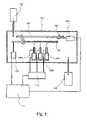
- FIG. 1is a diagram illustrating the structure of an evaporation device
- FIG. 2is a diagram illustrating an evaporation cell and an evaporation method
- FIG. 3is a diagram illustrating an apparatus used in manufacturing a light-emitting device
- FIGS. 4A and 4Bare diagrams showing the structure of an EL display device, where FIG. 4A is a top view thereof and FIG. 4B is a sectional view thereof;
- FIGS. 5A and 5Bare sectional views showing a pixel portion of an EL display device
- FIGS. 6A and 6Bare a top view of a pixel portion of an EL display device and a circuit diagram thereof, respectively;
- FIGS. 7A to 7Fare diagrams showing examples of a semiconductor device.
- FIGS. 8A to 8Care diagrams showing examples of the semiconductor device.
- FIG. 1is a diagram illustrating the structure of a gasification evaporation device according to the present invention.
- a reaction chamber 101is an air-tight container and the interior thereof is completely shut out from the outside air.
- the reaction chamber 101is filled with inert gas (typically, argon) supplied from gas introducing means 107 .
- the gasis kept at the same pressure as the atmospheric pressure (1.01 ⁇ 10 5 Pa).
- Discharging means 108is activated as the need arises to circulate the inert gas or to discharge the gas.
- One or plural evaporation cells used as evaporation sourcesare provided depending on the need.
- an evaporation cell (1) 109 aan evaporation cell (1) 109 a , an evaporation cell (2) 109 b , and an evaporation cell (3) 109 c , three in total, are provided.
- the temperature of these evaporation cellsis controlled by heating means 110 .
- a substrate 102is fixed to a sample stage 103 .
- a shutter automatically opening and closingis interposed between the substrate and the evaporation cells.
- a computer 111centrally controls control means 104 for moving the sample stage 103 in the horizontal direction, control means 106 for opening and closing the shutter 105 , and the heating means 110 , which operate in association with one another. The associated operation makes it possible to form a pre-programmed evaporation pattern on the substrate 102 without using a shadow mask.
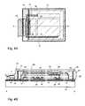
- FIG. 2is a diagram given for a simple explanation of this gasification evaporation.
- Evaporation cells 206 to 208contain evaporation materials and are heated to the evaporation temperature.
- Each evaporation cellis formed of boron nitride, alumina, tungsten, or the like, and has its tip formed into an orifice with a diameter of several tens to several hundreds ⁇ m.
- the pressure in the evaporation cellsis risen to gasify the contained materials and the flux distribution of the evaporation materials ejected through the orifices gains directivity.
- the directivityis determined in accordance with the orifice diameter and the thickness thereof. Since the deposition takes place under the atmospheric pressure, the gasified and evaporation materials have small mean free process and the evaporation materials can be deposited on the substrate while maintaining a relatively high directivity.
- the position of the substrate and the orificeis controlled so that evaporation films 209 to 212 are formed at positions that coincide with positions of pixel electrodes 202 to 204 formed on a substrate 201 .
- a bump 205is useful in separating adjoining evaporation films.
- a given pattern of evaporation filmscan be formed on a substrate without using a shadow mask.
- the patterncan have a width of about 50 to 200 ⁇ m.
- the substrateis placed on a sample stage and hence is movable in the horizontal direction (direction X-Y).
- direction X-YBy associating the movement of the substrate with opening and closing of the shutter and by using the evaporation cells illustrated in FIG. 2 , minute patterns can be drawn on a large-area substrate.
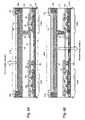
- reference symbol 501denotes a transfer chamber and the transfer chamber 501 is provided with a transferring mechanism 502 to carry a substrate 503 .
- the interior of the transfer chamber 501is set to the atmospheric pressure and is filled with inert gas.
- Gates 500 a to 500 eeach separate one processing chamber from other chambers.
- the substrateis carried from one processing chamber to another by the transferring mechanism 502 when the associated gate is opened.
- Reference symbol 504denotes a loading chamber for setting the substrate and the loading chamber also serves as an unloading chamber.
- the loading chamber 504is connected to the transfer chamber 501 through the gate 500 a , and this is where a carrier (not shown) in which the substrate 503 is set is placed.
- the loading chamber 504may be divided into a room for bringing the substrate in and a room for sending the substrate out.
- the substrate 503 supplied to the apparatushas finished the manufacture process up through formation of a transparent conductive film to serve as an anode of an EL element.
- the substrate 503is set in the carrier with its film forming surface facing downward. This is to facilitate a face down method (also called deposit up method) at a later step of forming a film by evaporation.
- the face down methodrefers to a method in which the film is formed while the film forming surface of the substrate faces downward. This method prevents dusts from settling onto the film forming surface.
- pre-processing chamber 505is a processing chamber for processing the surface of the anode of the EL element or a cathode thereof (hereinafter referred to as pre-processing chamber).
- the pre-processing chamber 505is connected to the transfer chamber 501 through the gate 500 b .
- the pre-processing chambercan be modified so as to suit a process of manufacturing an EL element, but any modified pre-processing chamber has to be capable of heating the substrate at 100 to 120° C. while irradiating the surface of the anode made of a transparent conductive film with ultraviolet light in oxygen. Pre-processing as such is effective in treating the surface of the anode of the EL element.
- the next processing chamberis an evaporation chamber denoted by 506 .
- the chamber 506is for depositing an organic EL material through evaporation and is called an evaporation chamber (A).
- the evaporation chamber (A) 506is connected to the transfer chamber 501 through the gate 500 c .
- the evaporation chamber (A) 506 provided herehas the structure shown in FIG. 1 .
- a hole injection layeris first formed over the entire surface of the substrate. Subsequently, a light emitting layer emitting red light is formed, then a light emitting layer emitting green light, and then a light emitting layer emitting blue light.
- the hole injection layer, the light emitting layer emitting red light, the light emitting layer emitting green light and the light emitting layer emitting blue lightcan be formed from arbitrary materials.
- the structure of the evaporation chamber (A) 506allows the evaporation sources to be switched in accordance with the kind of organic materials to be deposited.
- a preparatory chamber 508 storing plural kinds of evaporation cellsis connected to the evaporation chamber (A) 506 so that its interior transferring mechanism can replace an evaporation cell in 506 with an evaporation cell in 508 . Accordingly, the evaporation cells are switched every time the organic EL materials to be deposited change.
- a shadow maskis moved by a distance corresponding to one pixel whenever the organic EL material forming the same mask is changed.
- the deposition method used in the evaporation chamber (A) 506is the one illustrated in FIGS. 1 and 2 .
- reference symbol 509denotes an evaporation chamber for forming by deposition a conductive film (metal film serving as the cathode) serving as the anode or cathode of the EL element, and the chamber 509 is called an evaporation chamber (B).
- the evaporation chamber (B) 509is connected to the transfer chamber 501 through the gate 500 d .
- the evaporation chamber (B) 509 provided herehas the structure shown in FIG. 2 .
- an Al—Li alloy filmfilm of an alloy of aluminum and lithium
- the gasification evaporationcan also be applied to formation of an alloy film as this.
- a processing chamber that comes nextis a sealing chamber (also called an enclosing chamber or a glove box) 511 , which is connected to the loading chamber 504 through the gate 500 e .
- a sealing chamberalso called an enclosing chamber or a glove box
- the final processing of sealing the EL element in an air-tight spaceis conducted. This processing is to protect the fabricated EL element against oxygen and moisture, and uses methods such as automatic sealing using a sealing member or sealing with a thermally-curable resin or a UV-curable resin.
- the sealing membercan be formed from a material such as glass, ceramics, plastics and metals, but the material has to be light-transmissive if the EL element emits light toward the sealing member side.
- the sealing memberis bonded to the substrate on which the EL element is formed by curing a thermally-curable resin or a UV-curable resin through heat treatment or irradiation of ultraviolet light.
- the air-tight spaceis thus formed. It is also effective to place a hygroscopic material represented by barium oxide in this air-tight space.
- the space between the sealing member and the substrate on which the EL element is formedmay be filled with a thermally-curable resin or a UV-curable resin.
- a thermally-curable resin or a UV-curable resinmay be filled with a thermally-curable resin or a UV-curable resin.
- the sealing chamber 511has therein a mechanism 512 for irradiating ultraviolet light (hereinafter referred to as ultraviolet light irradiation mechanism).
- the ultraviolet light irradiation mechanism 512emits ultraviolet light to cure the UV-curable resin.
- the interior of the sealing chamber 511may be set to reduced pressure if a vacuum pump is provided. When the above sealing step is automated through operation of robots, the reduced pressure in the sealing chamber prevents oxygen and moisture from entering the chamber.
- the interior of the sealing chamber 511may be pressurized. In this case, it is pressurized while being purged with nitrogen gas or rare gas of high purity to prevent oxygen and the like of the outside air from entering the chamber.
- a handing-over chamber (pass box) 513is connected to the sealing chamber 511 .
- the handing-over chamber 513is provided with a transferring mechanism (B) 514 , which brings the substrate whose EL element has been enclosed through the processing in the sealing chamber 511 into the handing-over chamber 513 .
- the interior of the handing-over chamber 513may also be set to reduced pressure if a vacuum pump is provided.
- the handing-over chamber 513is provided to avoid direct exposure of the sealing chamber 511 to the outside air, and the substrate is taken out from the handing-over chamber.
- the film forming apparatus shown in FIG. 3is capable of keeping the substrate away from the outside air until after the EL element is completely enclosed in an air-tight space. This make the film forming apparatus capable of manufacturing an EL display device of higher reliability.
- FIG. 4Ais a top view of the EL display device.
- reference symbol 10denotes a substrate, 11 , a pixel portion, 12 , a source side driver circuit, and 13 , a gate side driver circuit.
- the driver circuitsare respectively led to an FPC 17 through wirings 14 to 16 and connected to external equipment.
- FIG. 4Bshows a sectional view taken along the line A-A′ of FIG. 4A .
- An opposite substrate 80is provided at least above the pixel portion, preferably, above the pixel portion and the driver circuits.
- the opposite substrate 80is bonded, using a sealing agent 19 , to an active matrix substrate on which TFT's and a light-emitting layer made of an EL material are formed.
- the sealing agent 19has a filler (not shown) mixed therein, which enables the two substrates to be bonded with an almost uniform distance.
- the exterior of the sealing agent 19 and the top and peripheral surface of the FPC 17are sealed with an enclosing agent 81 .
- the enclosing agent 81is formed from a silicone resin, an epoxy resin, a phenol resin, butyl rubber, or the like.
- the filling agent 83also has an effect of adhering the opposite substrate 80 .
- PVCpolyvinyl chloride
- an epoxy resinepoxy resin
- a silicone resinsilicone resin
- PVBpolyvinyl butylal
- EVAethylene vinylacetate
- the light-emitting layeris weak against moisture or humidity and is liable to degrade. Therefore it is desirable to mix a drying agent such as barium oxide in the filling agent 83 to maintain the moisture absorbing effect.
- a silicon nitride film or a silicon oxynitride filmis formed as a passivation film 82 on the light-emitting layer in order to prevent corrosion caused by an alkaline element contained in the filling agent 83 .
- the opposite substrate 80may be a glass plate, an aluminum plate, a stainless-steel plate, an FRP (fiberglass-reinforced plastics) plate, a PVF (polyvinyl fluoride) film, a Mylar film (trade name for a product of DuPont), a polyester film, an acrylic film, an acrylic plate, or the like.
- a sheet consisting of aluminum foil several tens ⁇ m in thickness and PVF films or Mylar films sandwiching the aluminum foilmay be used to enhance resistance against moisture. The EL element is thus sealed and shut out from the outside air.
- a driver circuit TFTshown here is a CMOS circuit using an n-channel TFT and a p-channel TFT in combination
- a pixel portion TFT(only a TFT for controlling a current to the EL element is shown here) 23 .
- the TFTs, the n-channel TFT in particular,have LDD regions structured as shown in this embodiment in order to prevent a decrease in ON current due to the hot carrier effect and to prevent characteristic degradation due to Vth shift and bias stress.
- an interlayer insulating film (leveling film) 26is formed from a resin material on a source wiring and a drain wiring.
- a pixel electrode 27 electrically connected to a drain of the pixel portion TFT 23is formed from a transparent conductive film.
- the transparent conductive filmmay contain a compound of indium oxide and a tin oxide (this compound is called ITO) or a compound of indium oxide and zinc oxide.
- an insulating film 28is formed and an opening is formed in the insulating film over the pixel electrode 27 .
- a light-emitting layer 29is then formed.
- the light-emitting layer 29may have a single layer structure or a laminate structure in which known EL materials to form a hole injection layer, a hole transportation layer, a light emitting layer, an electron transportation layer and an electron injection layer are layered in an arbitrary combination. Whichever structure is to be formed, known techniques can be used.
- the EL materials preferable for the present inventionare small molecular materials and are deposited by gasification evaporation.
- wavelengths of light emitted from light emitting layersare different between different pixels, thereby enabling the device to display in color.
- Other methods to obtain color displayinclude combining a color conversion layer (CCM) with color filters and combining a white light emitting layer with color filters, and either one can be employed.
- the EL display devicemay of course be a monochrome light emitting display device.
- a cathode 30is formed thereon. Desirably, moisture and oxygen in the interface between the cathode 30 and the light-emitting layer 29 are removed as much as possible. This requires some cotrivance such as forming the light-emitting layer 29 and the cathode 30 successively in vacuum or forming the light-emitting layer 29 in an inert atmosphere to then form the cathode 30 in vacuum without exposing it to the air.
- the film formation as abovecan be carried out by using a film forming apparatus of multi-chamber type.
- Yyttrium
- the cathode 30is connected to the wiring 16 in a region denoted by 31 .
- the wiring 16is a power supply line for applying a given voltage to the cathode 30 , and is connected to the FPC 17 through anisotropic conductive paste material 32 .
- a resin layer 80is formed on the FPC 17 to enhance the adhesion of this portion.
- a contact holehas to be formed through the interlayer insulating film 26 and the insulating film 28 .
- the contact holeis formed when the interlayer insulating film 26 is etched (upon forming a contact hole for the pixel electrode) and when the insulating film 28 is etched (upon forming the opening prior to the formation of the light-emitting layer).
- the contact holemay be formed by etching the insulating film 28 all the way through the interlayer insulating film 26 . In this case, the contact hole can be shaped appropriately if the interlayer insulating film 26 and the insulating film 28 are formed from the same resin material.
- the wiring 16passes through a gap between the sealing agent 19 and the substrate 10 (the gap is filled with the enclosing agent 81 ) to be electrically connected to the FPC 17 .
- the description given hereis about the wiring 16
- the other wirings 14 and 15similarly pass under the sealing agent 19 to be electrically connected to the FPC 17 .
- FIGS. 5A and 5Beach show a more detailed sectional structure of the pixel portion.
- FIG. 6A and FIG. 6Bshow a top structure of the pixel portion and a circuit diagram thereof, respectively.
- a switching TFT 2402 formed on a substrate 2401has a double gate structure in which substantially two TFTs are connected in series. An LDD region having an offset region that does not overlap with a gate electrode can thus be formed, thereby providing an advantage of reduced OFF current value.
- the TFThere has a double gate structure, it may take a triple gate structure or a multi-gate structure having more than three gates.
- An n-channel TFTis used for a current controlling TFT 2403 .
- This TFThas a structure in which an LDD region overlapping with a gate electrode is formed only on the drain side.
- the structurereduces the parasitic capacitance between the gate and the drain and reduces the serial resistance, thereby increasing a current driving ability.
- This structureis also significant from another viewpoint.
- the current controlling TFTis an element for controlling the amount of current flowing into the EL element, and hence a large amount of current flows through the TFT to increase the risk of degradation by heat or by hot carriers. Therefore, the degradation of the current controlling TFT is prevented and stability in operation of the current controlling TFT can be improved by providing it with an LDD region partially overlapping with a gate electrode.
- a drain 35 of the switching TFT 2402is electrically connected to a gate electrode 37 of the current controlling TFT through a wiring 36 .
- a wiring denoted by 38is a gate line for electrically connecting gate electrodes 39 a and 39 b of the switching TFT 2402 with each other.
- the current controlling TFT 2403 shown herehas a single gate structure. However, it may take a multi-gate structure in which a plurality of TFTs are connected in series. Another structure may be employed in which a plurality of TFTs are connected in parallel to substantially divide a channel forming region into plural sections, thereby releasing heat with high efficiency. This structure is effective as countermeasures against degradation by heat.
- a wiring serving as the gate electrode 37 of the current controlling TFT 2403overlaps with a drain line 40 of the current controlling TFT 2403 in a region denoted by 2404 through the insulating film.
- a capacitoris formed in the region denoted by 2404 .
- the capacitor 2404functions as a capacitor for holding the voltage applied to the gate of the current controlling TFT 2403 .
- the drain line 40is connected to a current supply line (power line) 2501 , and the voltage applied to the drain line 40 is kept constant.
- a first passivation film 41is formed on the switching TFT 2402 and the current controlling TFT 2403 .
- a leveling film 42is formed from a resin insulating film on the first passivation film. It is very important to level the level difference caused by the TFTs with the leveling film 42 . If the level difference exists, defective light emission may take place because the light-emitting layer to be subsequently formed is very thin. Therefore it is desirable to even out the level difference before forming the pixel electrode so that the light-emitting layer can be formed on as flat surface as possible.
- Denoted by 43is a pixel electrode (cathode of the EL element) formed of a highly reflective conductive film.
- the pixel electrode 43is electrically connected to the drain of the current controlling TFT 2403 .
- a low resistant conductive filmsuch as an aluminum alloy film, a copper alloy film and a silver alloy film, or a laminate film obtained by layering these alloy films is preferably used for the pixel electrode 43 .
- the pixel electrodemay of course be a laminate film of the low resistant conductive film and other conductive films.
- An insulating film(preferably a resin film) is used to form banks 44 a and 44 b , which form a groove (corresponding to a pixel) therebetween.
- a light emitting layer 45is formed in the groove.
- FIG. 6Ashows only one pixel, light emitting layers each emitting one of red light, green light and blue light may be formed separately.
- the light-emitting layer emitting white lightis composed of a hole injection layer 46 formed of PEDOT (polythiophene) or Pani (polyaniline), a blue light emitting layer formed of STAD, a green and red light emitting layer formed of Alq 3 +DCM, and an electron transportation layer formed of Alq 3 . These are small molecular materials and can be deposited successively by gasification evaporation.
- the light-emitting layerthus has a laminate structure in which the hole injection layer 46 formed of PEDOT (polythiophene) or Pani (polyaniline) is layered on the light emitting layer 45 .
- an anode 47is formed from a transparent conductive film.
- the anodehas to be light-transmissive because light generated in the light emitting layer 45 is emitted upward (toward the space above the TFTs).
- the transparent conductive filmmay contain a compound of indium oxide and tin oxide or a compound of an indium oxide and zinc oxide.
- Preferable material for the transparent conductive filmis the one that can be deposited at as low temperature as possible, for the transparent conductive film is formed after forming the light emitting layer and the hole injection layer that have low heat resistance.
- the anode 47is thus formed to complete a light-emitting element, namely, EL element 2405 .
- the EL element 2405here refers to a capacitor consisting of the pixel electrode (cathode) 43 , the light emitting layer 45 , the hole injection layer 46 and the anode 47 .
- the pixel electrode 43covers almost the entire area of the pixel as shown in FIG. 6A , and hence the whole pixel functions as the EL element. Accordingly, efficiency in utilization of light emission is very high to provide bright image display.
- a second passivation film 48is further formed on the anode 47 .
- the second passivation film 48is preferably a silicon nitride film or a silicon oxynitride film.
- the second passivation filmis provided in order to cut communication between the EL element and the outside, thereby preventing degradation of the organic EL material due to oxidation as well as preventing degassing from the organic EL material. This enhances the reliability of the EL display device.
- the EL display device of the present inventionhas a pixel portion composed of pixels that have the structure shown in FIGS. 6A and 6B , and has a switching TFT that has a sufficiently low OFF current value and a current controlling TFT that is strong against hot carrier injection.
- the EL display devicetherefore has high reliability and is capable of quality image display.
- FIG. 5Bshows an example in which the structure of the light-emitting layer is inverted.
- a p-channel TFTis used for a current controlling TFT 2601 .
- a transparent conductive filmis used to form a pixel electrode (anode) 50 .
- a conductive film of a compound of indium oxide and zinc oxideis used.
- a conductive film of a compound of indium oxide and tin oxidemay be used instead.
- the aforementioned light-emitting layer emitting white lightis formed.
- a cathode 54serves also as a passivation film.
- An EL element 2602is thus completed.
- the light generated in a light emitting layer 53 in this caseis emitted toward a substrate on which the TFT is formed as indicated by the arrow.
- the current controlling TFT 2601is preferably a p-channel TFT.
- the method according to this embodimentincludes moving the evaporation cells and the substrate relative to each other and providing a mechanism for associating opening and closing of the shutter with the movement. Therefore, a light emitting layer can be formed from an organic electroluminescence material on a large-area substrate to manufacture an EL display device.
- the light-emitting device formed through carrying out the manufacturing method of the present inventionmay be applied to various electro-optical devices.
- the present inventioncan be employed in electronic equipment that incorporate those electro-optical devices and the semiconductor circuits as the parts.
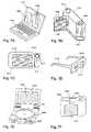
- a video camera, a digital camera, a projector (rear type or front type) a head mount display (goggle-type display), a navigation system for vehicles, a car stereo, a personal computer, and a portable information terminal (a mobile computer, a cellular phone, or an electronic book, etc.)may be enumerated. Examples of those are shown in FIGS. 7A to 7F and FIGS. 8A to 8C .
- FIG. 7Ashows a personal computer, and includes a main body 1201 , an image inputting portion 1202 , a display portion 1203 , a keyboard 1204 , and the like.
- the present inventionis applicable to the manufacture of the display portion 1203 .
- FIG. 7Bshows a video camera, and includes a main body 1205 , a display portion 1206 , a voice input portion 1207 , operation switches 1208 , a battery 1209 , and an image receiving portion 1210 .
- the present inventionis applicable to the manufacture of the display portion 1206 .
- FIG. 7Cshows a mobile computer, and includes a main body 1211 , a camera portion 1212 , an image receiving portion 1213 , an operation switch 1214 , and a display portion 1215 .
- the present inventionis applicable to the manufacture of the display portion 1215 .
- FIG. 7Dshows a goggle-type display, and includes a main body 1216 , a display portion 1217 and arm portions 1218 .
- the present inventionis applicable to the manufacture of the display portion 1217 .
- FIG. 7Eshows a player that employs a recording medium in which programs are recorded (hereinafter referred to as a recording medium), and includes a main body 1219 , a display portion 1220 , a speaker portion 1221 , a recording medium 1222 , an operation switch 1223 , and the like.
- this deviceuses as the recording medium a DVD (digital versatile disc), a CD and the like to serve as a tool for enjoying music or movies, for playing video games and for connecting to the Internet.
- the present inventionis applicable to the manufacture of the display portion 1220 .
- FIG. 7Fshows a digital camera, and includes a main body 1224 , a display unit 1225 , an eye contact portion 1226 , operation switches 1227 , and an image receiving unit (not shown) and the like.
- the present inventionis applicable to the manufacture of the display portion 1225 .
- FIG. 8Ashows a cellular phone, and includes a display panel 1401 , an operation panel 1402 , a connection portion 1403 , a display device 1404 , an audio output portion 1405 , operation keys 1406 , a power switch 1407 , an audio input portion 1408 , an antenna 1409 , and the like.
- the present inventionis applicable to the display device 1404 .
- FIG. 8Bshows a portable book (electronic book), and includes a main body 1411 , display portions 1412 , a recording medium 1413 , operation switches 1414 , an antenna 1415 , and the like.
- the present inventionis applicable to the manufacture of the display portion 1412 .
- FIG. 8Cshows a display, and includes a main body 1416 , a support stand 1417 , and a display portion 1418 .
- the present inventioncan be applied to the display portion 1418 .
- the display of the present inventionis advantageous for cases of large size screens in particular, and is advantageous for displays having a diagonal equal to or greater than 10 inches (in particular, equal to or greater than 30 inches).
- the evaporation cell and the substrateare relatively moved, with the result that the organic electroluminescence layer can be uniformly formed on the large area substrate having one side exceeding 1 m. Therefore, the present invention makes it easy to manufacture the large-sized display easier.
- application fields of the present inventionis extremely broad, and is capable of being applied to every fields of electronic equipment.
- the evaporation cell and the substrateare relatively moved, and the movement is associated with of the shutter, which makes it possible to form the layer consisting of the organic electroluminescence material on the large-sized substrate to thereby manufacture the EL display device.
- the present inventionmakes it possible to form, without using any shadow mask, a thin film having a highly uniform thickness throughout the substrate surface with high throughput.
Landscapes
- Chemical & Material Sciences (AREA)
- Engineering & Computer Science (AREA)
- Chemical Kinetics & Catalysis (AREA)
- Materials Engineering (AREA)
- Mechanical Engineering (AREA)
- Metallurgy (AREA)
- Organic Chemistry (AREA)
- Physics & Mathematics (AREA)
- Optics & Photonics (AREA)
- Manufacturing & Machinery (AREA)
- Electroluminescent Light Sources (AREA)
Abstract
Description
Claims (28)
Applications Claiming Priority (2)
| Application Number | Priority Date | Filing Date | Title |
|---|---|---|---|
| JP2000141005 | 2000-05-12 | ||
| JP2000-141005 | 2000-05-12 |
Publications (2)
| Publication Number | Publication Date |
|---|---|
| US20020009538A1 US20020009538A1 (en) | 2002-01-24 |
| US7517551B2true US7517551B2 (en) | 2009-04-14 |
Family
ID=18648193
Family Applications (1)
| Application Number | Title | Priority Date | Filing Date |
|---|---|---|---|
| US09/847,308Expired - Fee RelatedUS7517551B2 (en) | 2000-05-12 | 2001-05-03 | Method of manufacturing a light-emitting device |
Country Status (1)
| Country | Link |
|---|---|
| US (1) | US7517551B2 (en) |
Cited By (5)
| Publication number | Priority date | Publication date | Assignee | Title |
|---|---|---|---|---|
| US20080316149A1 (en)* | 2006-12-29 | 2008-12-25 | In Hwan Kim | Electro-luminescence pixel, panel with the pixel, and device and method for driving the panel |
| US20100236691A1 (en)* | 2009-03-18 | 2010-09-23 | Semiconductor Energy Laboratory Co., Ltd. | Manufacturing Apparatus and Manufacturing Method of Lighting Device |
| US20100237805A1 (en)* | 2009-03-18 | 2010-09-23 | Semiconductor Energy Laboratory Co., Ltd. | Lighting Device |
| US20150161943A1 (en)* | 2013-12-09 | 2015-06-11 | Lg Display Co., Ltd. | Organic light emitting display device having repair structure |
| US20180298489A1 (en)* | 2014-03-11 | 2018-10-18 | Joled Inc. | Deposition apparatus, method for controlling same, deposition method using deposition apparatus, and device manufacturing method |
Families Citing this family (48)
| Publication number | Priority date | Publication date | Assignee | Title |
|---|---|---|---|---|
| US7197570B2 (en)* | 1998-07-22 | 2007-03-27 | Appstream Inc. | System and method to send predicted application streamlets to a client device |
| US20010044850A1 (en)* | 1998-07-22 | 2001-11-22 | Uri Raz | Method and apparatus for determining the order of streaming modules |
| US8706630B2 (en)* | 1999-08-19 | 2014-04-22 | E2Interactive, Inc. | System and method for securely authorizing and distributing stored-value card data |
| TW490714B (en)* | 1999-12-27 | 2002-06-11 | Semiconductor Energy Lab | Film formation apparatus and method for forming a film |
| US20020011205A1 (en)* | 2000-05-02 | 2002-01-31 | Shunpei Yamazaki | Film-forming apparatus, method of cleaning the same, and method of manufacturing a light-emitting device |
| US7051315B2 (en) | 2000-09-26 | 2006-05-23 | Appstream, Inc. | Network streaming of multi-application program code |
| US20030146692A1 (en)* | 2002-01-11 | 2003-08-07 | Seiko Epson Corporation | Organic EL device and manufacturing method therefor, electrooptic apparatus, and electronic apparatus |
| JP4066661B2 (en) | 2002-01-23 | 2008-03-26 | セイコーエプソン株式会社 | Organic EL device manufacturing apparatus and droplet discharge apparatus |
| TWI262034B (en)* | 2002-02-05 | 2006-09-11 | Semiconductor Energy Lab | Manufacturing system, manufacturing method, method of operating a manufacturing apparatus, and light emitting device |
| TWI285515B (en)* | 2002-02-22 | 2007-08-11 | Semiconductor Energy Lab | Light-emitting device and method of manufacturing the same, and method of operating manufacturing apparatus |
| SG113448A1 (en)* | 2002-02-25 | 2005-08-29 | Semiconductor Energy Lab | Fabrication system and a fabrication method of a light emitting device |
| JP3877613B2 (en)* | 2002-03-05 | 2007-02-07 | 三洋電機株式会社 | Method for manufacturing organic electroluminescence display device |
| US7309269B2 (en)* | 2002-04-15 | 2007-12-18 | Semiconductor Energy Laboratory Co., Ltd. | Method of fabricating light-emitting device and apparatus for manufacturing light-emitting device |
| TWI336905B (en)* | 2002-05-17 | 2011-02-01 | Semiconductor Energy Lab | Evaporation method, evaporation device and method of fabricating light emitting device |
| US20040035360A1 (en)* | 2002-05-17 | 2004-02-26 | Semiconductor Energy Laboratory Co., Ltd. | Manufacturing apparatus |
| US20030221620A1 (en)* | 2002-06-03 | 2003-12-04 | Semiconductor Energy Laboratory Co., Ltd. | Vapor deposition device |
| US6943066B2 (en)* | 2002-06-05 | 2005-09-13 | Advantech Global, Ltd | Active matrix backplane for controlling controlled elements and method of manufacture thereof |
| US6858464B2 (en) | 2002-06-19 | 2005-02-22 | Semiconductor Energy Laboratory Co., Ltd. | Method of manufacturing light emitting device |
| US20040040504A1 (en)* | 2002-08-01 | 2004-03-04 | Semiconductor Energy Laboratory Co., Ltd. | Manufacturing apparatus |
| TWI277363B (en)* | 2002-08-30 | 2007-03-21 | Semiconductor Energy Lab | Fabrication system, light-emitting device and fabricating method of organic compound-containing layer |
| TWI252706B (en)* | 2002-09-05 | 2006-04-01 | Sanyo Electric Co | Manufacturing method of organic electroluminescent display device |
| US20040123804A1 (en)* | 2002-09-20 | 2004-07-01 | Semiconductor Energy Laboratory Co., Ltd. | Fabrication system and manufacturing method of light emitting device |
| CN100544533C (en)* | 2002-11-11 | 2009-09-23 | 株式会社半导体能源研究所 | Method for manufacturing light emitting device |
| WO2004054325A1 (en)* | 2002-12-12 | 2004-06-24 | Semiconductor Energy Laboratory Co., Ltd. | Light-emitting device, manufacturing apparatus, film-forming method, and cleaning method |
| CN1732714B (en)* | 2002-12-26 | 2011-07-13 | 株式会社半导体能源研究所 | Light emitting device |
| US7211461B2 (en)* | 2003-02-14 | 2007-05-01 | Semiconductor Energy Laboratory Co., Ltd. | Manufacturing apparatus |
| JP4493926B2 (en) | 2003-04-25 | 2010-06-30 | 株式会社半導体エネルギー研究所 | Manufacturing equipment |
| US7735057B2 (en)* | 2003-05-16 | 2010-06-08 | Symantec Corporation | Method and apparatus for packaging and streaming installation software |
| US7211454B2 (en)* | 2003-07-25 | 2007-05-01 | Semiconductor Energy Laboratory Co., Ltd. | Manufacturing method of a light emitting device including moving the source of the vapor deposition parallel to the substrate |
| JP4366226B2 (en)* | 2004-03-30 | 2009-11-18 | 東北パイオニア株式会社 | Organic EL panel manufacturing method, organic EL panel film forming apparatus |
| US9124653B2 (en)* | 2004-09-03 | 2015-09-01 | Symantec Corporation | Method and apparatus for allowing sharing of streamable applications |
| KR101133758B1 (en)* | 2005-01-19 | 2012-04-09 | 삼성전자주식회사 | Sensor and thin film transistor array panel including sensor |
| US7948171B2 (en)* | 2005-02-18 | 2011-05-24 | Semiconductor Energy Laboratory Co., Ltd. | Light emitting device |
| US7271111B2 (en)* | 2005-06-08 | 2007-09-18 | Advantech Global, Ltd | Shadow mask deposition of materials using reconfigurable shadow masks |
| JP4789551B2 (en)* | 2005-09-06 | 2011-10-12 | 株式会社半導体エネルギー研究所 | Organic EL film forming equipment |
| US7531470B2 (en)* | 2005-09-27 | 2009-05-12 | Advantech Global, Ltd | Method and apparatus for electronic device manufacture using shadow masks |
| JP4974504B2 (en)* | 2005-10-13 | 2012-07-11 | 株式会社半導体エネルギー研究所 | Film forming apparatus and light emitting apparatus manufacturing method |
| US8354674B2 (en)* | 2007-06-29 | 2013-01-15 | Semiconductor Energy Laboratory Co., Ltd. | Semiconductor device wherein a property of a first semiconductor layer is different from a property of a second semiconductor layer |
| JP4085127B1 (en)* | 2007-10-02 | 2008-05-14 | 株式会社エムアンドシー | Removal suction device |
| JP5409652B2 (en)* | 2008-12-09 | 2014-02-05 | 株式会社アルバック | Method for forming tantalum nitride film |
| KR100994118B1 (en)* | 2009-01-13 | 2010-11-15 | 삼성모바일디스플레이주식회사 | Organic light emitting device and method for manufacturing same |
| EP2447393A1 (en)* | 2010-10-27 | 2012-05-02 | Applied Materials, Inc. | Evaporation system and method |
| WO2012118199A1 (en)* | 2011-03-03 | 2012-09-07 | 東京エレクトロン株式会社 | Vapor-deposition device, vapor-deposition method, organic el display, and lighting device |
| KR101810046B1 (en)* | 2012-01-19 | 2017-12-19 | 삼성디스플레이 주식회사 | Vapor deposition apparatus and method for vapor deposition |
| KR101968664B1 (en)* | 2012-08-06 | 2019-08-14 | 삼성디스플레이 주식회사 | Device for forming thin layer and manufacturing method of organic light emitting diode display using the same |
| US20140052613A1 (en)* | 2012-08-17 | 2014-02-20 | Square, Inc., A Delaware Corporation | Systems and methods for providing gratuities to merchants |
| KR101325864B1 (en)* | 2012-08-27 | 2013-11-05 | 에스엔유 프리시젼 주식회사 | Evaporating apparatus using for organic light emitting diode encapsulating process |
| KR20150006725A (en)* | 2013-07-09 | 2015-01-19 | 삼성디스플레이 주식회사 | Thin film deposition apparatus and manufacturing method of organic light emitting diode display using the same |
Citations (149)
| Publication number | Priority date | Publication date | Assignee | Title |
|---|---|---|---|---|
| US2351536A (en) | 1941-04-25 | 1944-06-13 | Spencer Lens Co | Method of treating surfaces |
| US2435997A (en) | 1943-11-06 | 1948-02-17 | American Optical Corp | Apparatus for vapor coating of large surfaces |
| US2906637A (en) | 1953-05-19 | 1959-09-29 | Electronique Soc Gen | Method of forming a film a short distance from a surface |
| US3312190A (en) | 1964-02-25 | 1967-04-04 | Burroughs Corp | Mask and substrate alignment apparatus |
| US3543717A (en) | 1968-04-25 | 1970-12-01 | Itek Corp | Means to adjust collimator and crucible location in a vapor deposition apparatus |
| US3756193A (en) | 1972-05-01 | 1973-09-04 | Battelle Memorial Institute | Coating apparatus |
| US3931490A (en) | 1973-09-17 | 1976-01-06 | Robert Bosch G.M.B.H. | Electron beam vaporization apparatus |
| US3931789A (en) | 1973-04-28 | 1976-01-13 | Canon Kabushiki Kaisha | Vapor deposition apparatus |
| US3971334A (en) | 1975-03-04 | 1976-07-27 | Xerox Corporation | Coating device |
| US4023523A (en) | 1975-04-23 | 1977-05-17 | Xerox Corporation | Coater hardware and method for obtaining uniform photoconductive layers on a xerographic photoreceptor |
| JPS54127877U (en) | 1978-02-26 | 1979-09-06 | ||
| US4187801A (en) | 1977-12-12 | 1980-02-12 | Commonwealth Scientific Corporation | Method and apparatus for transporting workpieces |
| DE2834806A1 (en) | 1978-08-09 | 1980-02-14 | Leybold Heraeus Gmbh & Co Kg | Vacuum vapour deposition of thin films esp. aluminium on TV tubes - using evaporator boat fitted on cardan mounting so that evaporator can be tilted |
| US4225805A (en) | 1978-12-22 | 1980-09-30 | Gte Products Corporation | Cathode ray tube getter sealing structure |
| US4233937A (en) | 1978-07-20 | 1980-11-18 | Mcdonnell Douglas Corporation | Vapor deposition coating machine |
| JPS57123973U (en) | 1981-01-27 | 1982-08-02 | ||
| US4405487A (en) | 1982-04-29 | 1983-09-20 | Harrah Larry A | Combination moisture and hydrogen getter |
| JPS58177463U (en) | 1982-05-21 | 1983-11-28 | 株式会社日本ロツク | Electronic lock chain lock |
| US4446357A (en) | 1981-10-30 | 1984-05-01 | Kennecott Corporation | Resistance-heated boat for metal vaporization |
| US4469719A (en) | 1981-12-21 | 1984-09-04 | Applied Magnetics-Magnetic Head Divison Corporation | Method for controlling the edge gradient of a layer of deposition material |
| JPS60121616U (en) | 1984-01-25 | 1985-08-16 | 三菱電機株式会社 | Tap switching device under load |
| US4543467A (en) | 1982-10-26 | 1985-09-24 | Balzers Aktiengesellschaft | Effusion type evaporator cell for vacuum evaporators |
| JPS6032361Y2 (en) | 1980-03-17 | 1985-09-27 | 三国工業株式会社 | Starter operation mechanism of multiple carburetor |
| JPS6115969Y2 (en) | 1980-12-26 | 1986-05-17 | ||
| US4592306A (en) | 1983-12-05 | 1986-06-03 | Pilkington Brothers P.L.C. | Apparatus for the deposition of multi-layer coatings |
| US4596735A (en) | 1983-04-30 | 1986-06-24 | Tdk Corporation | Magnetic recording medium and method for making |
| US4602192A (en) | 1983-03-31 | 1986-07-22 | Matsushita Electric Industrial Co., Ltd. | Thin film integrated device |
| US4627989A (en) | 1983-08-20 | 1986-12-09 | Leybold Heraeus Gmbh | Method and system for a vacuum evaporative deposition process |
| US4672265A (en)* | 1984-07-31 | 1987-06-09 | Canon Kabushiki Kaisha | Electroluminescent device |
| JPS6379959U (en) | 1986-11-14 | 1988-05-26 | ||
| US4769292A (en) | 1987-03-02 | 1988-09-06 | Eastman Kodak Company | Electroluminescent device with modified thin film luminescent zone |
| JPS63186763U (en) | 1987-02-16 | 1988-11-30 | ||
| JPS6442392U (en) | 1987-09-03 | 1989-03-14 | ||
| US4885211A (en) | 1987-02-11 | 1989-12-05 | Eastman Kodak Company | Electroluminescent device with improved cathode |
| US4897290A (en) | 1986-09-26 | 1990-01-30 | Konishiroku Photo Industry Co., Ltd. | Method for manufacturing the substrate for liquid crystal display |
| JPH02173261A (en) | 1988-12-26 | 1990-07-04 | Komatsu Ltd | Vacuum film forming equipment |
| US4951601A (en) | 1986-12-19 | 1990-08-28 | Applied Materials, Inc. | Multi-chamber integrated process system |
| JPH04116169A (en) | 1990-09-05 | 1992-04-16 | Shin Meiwa Ind Co Ltd | Vacuum vapor deposition device for forming multilayered films |
| JPH04268069A (en) | 1991-02-22 | 1992-09-24 | Konica Corp | Vapor deposition device |
| US5190590A (en) | 1990-04-10 | 1993-03-02 | Matsushita Electric Industrial Co., Ltd. | Vacuum coating apparatus |
| US5225238A (en)* | 1990-03-08 | 1993-07-06 | Rhone-Poulenc Nutrition Animale | Method for coating active principles with a ph-sensitive polymer |
| US5258325A (en) | 1990-12-31 | 1993-11-02 | Kopin Corporation | Method for manufacturing a semiconductor device using a circuit transfer film |
| US5259881A (en) | 1991-05-17 | 1993-11-09 | Materials Research Corporation | Wafer processing cluster tool batch preheating and degassing apparatus |
| JPH05304197A (en) | 1992-04-27 | 1993-11-16 | Hitachi Ltd | Multi-chamber system |
| US5294870A (en)* | 1991-12-30 | 1994-03-15 | Eastman Kodak Company | Organic electroluminescent multicolor image display device |
| US5310410A (en) | 1990-04-06 | 1994-05-10 | Sputtered Films, Inc. | Method for processing semi-conductor wafers in a multiple vacuum and non-vacuum chamber apparatus |
| JPH06306181A (en) | 1993-03-12 | 1994-11-01 | Agency Of Ind Science & Technol | Process and apparatus for producing organic optical thin film |
| JPH0688233B2 (en) | 1984-09-20 | 1994-11-09 | オスカ−・メイヤ−・フツヅ・コ−ポレ−シヨン | Chiyotsu Blade Assembly |
| JPH0718426Y2 (en) | 1990-05-30 | 1995-05-01 | 本田技研工業株式会社 | Clamp device |
| US5429884A (en) | 1992-01-17 | 1995-07-04 | Pioneer Electronic Corporation | Organic electroluminescent element |
| JPH07192866A (en) | 1993-12-26 | 1995-07-28 | Ricoh Co Ltd | Organic thin film electroluminescent device |
| JPH07252671A (en) | 1994-03-09 | 1995-10-03 | Agency Of Ind Science & Technol | Production of composite type optical thin film and apparatus for producing the same |
| DE4422697C1 (en) | 1994-06-29 | 1996-01-25 | Zsw | Vapour coating device for prodn. of thin filmed solar cells |
| US5512320A (en) | 1993-01-28 | 1996-04-30 | Applied Materials, Inc. | Vacuum processing apparatus having improved throughput |
| JPH08111285A (en) | 1994-10-07 | 1996-04-30 | Tdk Corp | Method and apparatus for manufacturing organic electroluminescent element |
| US5534314A (en)* | 1994-08-31 | 1996-07-09 | University Of Virginia Patent Foundation | Directed vapor deposition of electron beam evaporant |
| US5550066A (en) | 1994-12-14 | 1996-08-27 | Eastman Kodak Company | Method of fabricating a TFT-EL pixel |
| JPH0916960A (en) | 1995-06-30 | 1997-01-17 | Hitachi Maxell Ltd | Information recording medium manufacturing equipment |
| US5643685A (en) | 1993-10-26 | 1997-07-01 | Fuji Xerox Co., Ltd. | Thin film electroluminescence element and process for producing the same |
| JPH09209127A (en) | 1996-02-05 | 1997-08-12 | Idemitsu Kosan Co Ltd | Vacuum deposition apparatus and method for manufacturing organic electroluminescence element using the vacuum deposition apparatus |
| US5670792A (en) | 1993-10-12 | 1997-09-23 | Nec Corporation | Current-controlled luminous element array and method for producing the same |
| JPH09256156A (en) | 1996-03-18 | 1997-09-30 | Miyota Kk | Film forming device |
| JPH09256142A (en) | 1996-03-15 | 1997-09-30 | Sony Corp | Film forming device |
| US5695564A (en) | 1994-08-19 | 1997-12-09 | Tokyo Electron Limited | Semiconductor processing system |
| US5701055A (en) | 1994-03-13 | 1997-12-23 | Pioneer Electronic Corporation | Organic electoluminescent display panel and method for manufacturing the same |
| JPH1041069A (en) | 1996-04-18 | 1998-02-13 | Toray Ind Inc | Manufacturing method of organic electroluminescent device |
| JPH10168559A (en) | 1996-12-06 | 1998-06-23 | Ulvac Japan Ltd | Organic thin film forming apparatus and method of recycling organic material |
| JPH10195639A (en)* | 1997-01-09 | 1998-07-28 | Ulvac Japan Ltd | Evaporation source for organic material and organic thin film forming apparatus using the same |
| JPH10214682A (en) | 1997-01-30 | 1998-08-11 | Mitsubishi Chem Corp | Manufacturing apparatus and manufacturing method for organic electroluminescent element |
| US5817366A (en) | 1996-07-29 | 1998-10-06 | Tdk Corporation | Method for manufacturing organic electroluminescent element and apparatus therefor |
| US5844363A (en)* | 1997-01-23 | 1998-12-01 | The Trustees Of Princeton Univ. | Vacuum deposited, non-polymeric flexible organic light emitting devices |
| WO1998054375A1 (en) | 1997-05-30 | 1998-12-03 | Lintek Pty. Ltd. | Vacuum deposition system including mobile source |
| JPH10335062A (en) | 1997-05-30 | 1998-12-18 | Tdk Corp | Device and method for manufacturing organic el element |
| US5902688A (en)* | 1996-07-16 | 1999-05-11 | Hewlett-Packard Company | Electroluminescent display device |
| US5904961A (en) | 1997-01-24 | 1999-05-18 | Eastman Kodak Company | Method of depositing organic layers in organic light emitting devices |
| US5906857A (en) | 1997-05-13 | 1999-05-25 | Ultratherm, Inc. | Apparatus, system and method for controlling emission parameters attending vaporized in a HV environment |
| US5921836A (en)* | 1996-05-09 | 1999-07-13 | Fujitsu Limited | Apparatus for forming fluorescent layers of a plasma display panel and method therefor |
| US5937272A (en) | 1997-06-06 | 1999-08-10 | Eastman Kodak Company | Patterned organic layers in a full-color organic electroluminescent display array on a thin film transistor array substrate |
| US5935395A (en) | 1995-11-08 | 1999-08-10 | Mitel Corporation | Substrate processing apparatus with non-evaporable getter pump |
| US5943600A (en) | 1995-03-13 | 1999-08-24 | Applied Materials, Inc. | Treatment of a titanium nitride layer to improve resistance to elevated temperatures |
| JPH11229123A (en) | 1998-02-12 | 1999-08-24 | Casio Comput Co Ltd | Vapor deposition equipment |
| US5945967A (en)* | 1995-01-18 | 1999-08-31 | I-O Display Systems, Llc | Speckle depixelator |
| US5972183A (en) | 1994-10-31 | 1999-10-26 | Saes Getter S.P.A | Getter pump module and system |
| US6001413A (en) | 1997-03-10 | 1999-12-14 | Idemitsu Kosan Co., Ltd. | Method for producing organic electroluminescent device |
| US6011904A (en) | 1997-06-10 | 2000-01-04 | Board Of Regents, University Of Texas | Molecular beam epitaxy effusion cell |
| US6023308A (en) | 1991-10-16 | 2000-02-08 | Semiconductor Energy Laboratory Co., Ltd. | Active matrix device with two TFT's per pixel driven by a third TFT with a crystalline silicon channel |
| US6049167A (en)* | 1997-02-17 | 2000-04-11 | Tdk Corporation | Organic electroluminescent display device, and method and system for making the same |
| US6101316A (en)* | 1998-05-28 | 2000-08-08 | Nihon Shinku Gijutsu Kabushiki Kaisha | Evaporation apparatus, organic material evaporation source, and method of manufacturing thin organic film |
| US6124215A (en) | 1997-10-06 | 2000-09-26 | Chartered Semiconductor Manufacturing Ltd. | Apparatus and method for planarization of spin-on materials |
| JP2000282219A (en) | 1999-04-02 | 2000-10-10 | Canon Inc | Method and apparatus for regenerating mask for vacuum deposition of organic film |
| US6132805A (en) | 1998-10-20 | 2000-10-17 | Cvc Products, Inc. | Shutter for thin-film processing equipment |
| US6132280A (en) | 1998-10-28 | 2000-10-17 | Tdk Corporation | System and process for fabricating an organic electroluminescent display device |
| US6149392A (en) | 1997-10-15 | 2000-11-21 | Saes Getters S.P.A. | Getter pump with high gas sorption velocity |
| JP2000328229A (en) | 1999-05-19 | 2000-11-28 | Canon Inc | Vacuum deposition equipment |
| JP2000348859A (en) | 1999-06-03 | 2000-12-15 | Chisso Corp | Organic electroluminescent element |
| EP1071117A2 (en) | 1999-07-23 | 2001-01-24 | Sel Semiconductor Energy Laboratory Co., Ltd. | Method of fabricating a display device, and apparatus for forming a thin film |
| US6179923B1 (en) | 1997-08-22 | 2001-01-30 | Fuji Electric Co., Ltd. | Deposition apparatus for an organic thin-film light-emitting element |
| JP2001089841A (en) | 1999-09-22 | 2001-04-03 | Sony Corp | Jig for surface working and surface working method |
| JP2001093667A (en) | 1999-09-28 | 2001-04-06 | Sanyo Electric Co Ltd | Organic light-emitting element, device and method for manufacturing the same |
| WO2001031081A1 (en) | 1999-10-22 | 2001-05-03 | Kurt J. Lesker Company | Method and apparatus for coating a substrate in a vacuum |
| US6237529B1 (en) | 2000-03-03 | 2001-05-29 | Eastman Kodak Company | Source for thermal physical vapor deposition of organic electroluminescent layers |
| JP2001152336A (en) | 1999-11-22 | 2001-06-05 | Minolta Co Ltd | Optical thin film manufacturing apparatus, and optical thin film manufacturing method |
| US6244212B1 (en) | 1999-12-30 | 2001-06-12 | Genvac Aerospace Corporation | Electron beam evaporation assembly for high uniform thin film |
| US20010006827A1 (en) | 1999-12-27 | 2001-07-05 | Semiconductor Energy Laboratory Co., Ltd. | Film formation apparatus and method for forming a film |
| JP2001185350A (en) | 1999-12-24 | 2001-07-06 | Sanyo Electric Co Ltd | Worn mask, its manufacturing method, electroluminescent display device and its manufacturing method |
| US20010009154A1 (en) | 1998-08-19 | 2001-07-26 | Tue Nguyen | In-situ method of cleaning a metal-organic chemical vapor deposition chamber |
| US6280861B1 (en) | 1996-05-29 | 2001-08-28 | Idemitsu Kosan Co., Ltd. | Organic EL device |
| US20010022272A1 (en) | 1998-08-03 | 2001-09-20 | George Plester | Methods for measuring the degree of ionization and the rate of evaporation in a vapor deposition coating system |
| US6294892B1 (en)* | 1998-12-22 | 2001-09-25 | Nec Corporation | Method of manufacturing organic thin-film EL device |
| US6296894B1 (en) | 1998-08-26 | 2001-10-02 | Tdk Corporation | Evaporation source, apparatus and method for the preparation of organic El device |
| US6299746B1 (en) | 1997-12-23 | 2001-10-09 | Saes Getters, S.P.A. | Getter system for purifying the confinement volume in process chambers |
| US6319321B1 (en) | 1997-01-20 | 2001-11-20 | Agency Of Industrial Science & Technology Ministry Of International Trade & Industry | Thin-film fabrication method and apparatus |
| US6326726B1 (en) | 1997-02-21 | 2001-12-04 | Nec Corporation | Organic electroluminescent display device having insulative shielding walls |
| US6333065B1 (en) | 1997-07-25 | 2001-12-25 | Tdk Corporation | Process for the production of an organic electroluminescent device |
| US6337105B1 (en) | 1997-07-14 | 2002-01-08 | Matsushita Electric Industrial Co., Ltd. | Method and apparatus for forming thin functional film |
| US6340501B1 (en) | 1997-05-08 | 2002-01-22 | Matsushita Electric Industrial Co., Ltd. | Device and method for manufacturing an optical recording medium |
| US20020011205A1 (en) | 2000-05-02 | 2002-01-31 | Shunpei Yamazaki | Film-forming apparatus, method of cleaning the same, and method of manufacturing a light-emitting device |
| WO2001079581A8 (en) | 2000-03-30 | 2002-02-14 | Idemitsu Kosan Co | Method for forming thin-film layer for device and organic electroluminescence device |
| US6380081B1 (en) | 1999-11-18 | 2002-04-30 | Genitech, Inc. | Method of vaporizing liquid sources and apparatus therefor |
| US6382895B1 (en) | 1998-12-28 | 2002-05-07 | Anelva Corporation | Substrate processing apparatus |
| US6403392B1 (en) | 1998-10-30 | 2002-06-11 | The Trustees Of Princeton University | Method for patterning devices |
| US20020076847A1 (en) | 2000-09-28 | 2002-06-20 | Tsutomu Yamada | Method of attaching layer material and forming layer in predetermined pattern on substrate using mask |
| US20020081372A1 (en) | 2000-11-07 | 2002-06-27 | Kuang-Chung Peng | Method for fabricating an organic light emitting diode |
| US20020084032A1 (en) | 1999-02-19 | 2002-07-04 | Taiwan Semiconductor Manufacturing Company | Multiple chamber vacuum processing system configuration for improving the stability of mark shielding process |
| US6432561B1 (en) | 1999-07-23 | 2002-08-13 | Semiconductor Energy Laboratory Co., Ltd. | EL display device and method of manufacturing the same |
| US6469439B2 (en) | 1999-06-15 | 2002-10-22 | Toray Industries, Inc. | Process for producing an organic electroluminescent device |
| US20020155632A1 (en) | 2001-02-21 | 2002-10-24 | Shunpei Yamazaki | Method and apparatus for film deposition |
| US6482852B2 (en) | 1998-11-12 | 2002-11-19 | Ariad Pharmaceuticals, Inc. | Bicyclic signal transduction inhibitors, compositions containing them & uses thereof |
| US6482752B1 (en) | 1993-10-26 | 2002-11-19 | Semiconductor Energy Laboratory Co., Ltd. | Substrate processing apparatus and method and a manufacturing method of a thin film semiconductor device |
| US20020179013A1 (en) | 2001-05-23 | 2002-12-05 | Junji Kido | Successive vapour deposition system, vapour deposition system, and vapour deposition process |
| US20020197418A1 (en) | 2001-06-26 | 2002-12-26 | Tokio Mizukami | Molecular beam epitaxy effusion cell for use in vacuum thin film deposition and a method therefor |
| JP2003017258A (en) | 2001-06-29 | 2003-01-17 | Sanyo Electric Co Ltd | Manufacturing method of electroluminescent display |
| US20030015140A1 (en) | 2001-04-26 | 2003-01-23 | Eastman Kodak Company | Physical vapor deposition of organic layers using tubular sources for making organic light-emitting devices |
| US20030024479A1 (en) | 2001-07-31 | 2003-02-06 | Fuji Photo Film Co., Ltd. | Vacuum deposition apparatus |
| JP2003034591A (en) | 2001-07-19 | 2003-02-07 | Nippon Biitec:Kk | Molecular beam source cell for depositing thin film |
| US6528108B1 (en) | 1999-09-27 | 2003-03-04 | Tokyo Electron Limited | Method and apparatus for observing porous amorphous film, and method and apparatus for forming the same |
| US6537607B1 (en)* | 1999-12-17 | 2003-03-25 | Texas Instruments Incorporated | Selective deposition of emissive layer in electroluminescent displays |
| JP2003095787A (en) | 2001-09-25 | 2003-04-03 | Nippon Biitec:Kk | Molecular beam source cell for depositing thin film |
| US20030101937A1 (en) | 2001-11-28 | 2003-06-05 | Eastman Kodak Company | Thermal physical vapor deposition source for making an organic light-emitting device |
| EP1319732A1 (en) | 2001-12-12 | 2003-06-18 | Semiconductor Energy Laboratory Co., Ltd. | Film formation apparatus and method and cleaning method |
| US20030180457A1 (en) | 2002-02-05 | 2003-09-25 | Semiconductor Energy Laboratory Co., Ltd. | Manufacturing system, manufacturing method, method of operating a manufacturing apparatus, and light emitting device |
| US6633121B2 (en) | 2000-01-31 | 2003-10-14 | Idemitsu Kosan Co., Ltd. | Organic electroluminescence display device and method of manufacturing same |
| US6641674B2 (en) | 2000-11-10 | 2003-11-04 | Helix Technology Inc. | Movable evaporation device |
| US20030219530A1 (en) | 2002-02-22 | 2003-11-27 | Shunpei Yamazaki | Light-emitting device and method of manufacturing the same, and method of operating manufacturing apparatus |
| US6660409B1 (en) | 1999-09-16 | 2003-12-09 | Panasonic Communications Co., Ltd | Electronic device and process for producing the same |
| US6696096B2 (en) | 2000-06-22 | 2004-02-24 | Matsushita Electric Works, Ltd. | Apparatus for and method of vacuum vapor deposition and organic electroluminescent device |
| US20040035366A1 (en) | 2002-07-23 | 2004-02-26 | Samsung Nec Mobile Display Co., Ltd. | Heating crucible and deposition apparatus using the same |
| US6830626B1 (en) | 1999-10-22 | 2004-12-14 | Kurt J. Lesker Company | Method and apparatus for coating a substrate in a vacuum |
| EP0955791B1 (en) | 1997-10-15 | 2005-08-31 | Toray Industries, Inc. | Process for manufacturing an organic electroluminescent device |
- 2001
- 2001-05-03USUS09/847,308patent/US7517551B2/ennot_activeExpired - Fee Related
Patent Citations (163)
| Publication number | Priority date | Publication date | Assignee | Title |
|---|---|---|---|---|
| US2351536A (en) | 1941-04-25 | 1944-06-13 | Spencer Lens Co | Method of treating surfaces |
| US2435997A (en) | 1943-11-06 | 1948-02-17 | American Optical Corp | Apparatus for vapor coating of large surfaces |
| US2906637A (en) | 1953-05-19 | 1959-09-29 | Electronique Soc Gen | Method of forming a film a short distance from a surface |
| US3312190A (en) | 1964-02-25 | 1967-04-04 | Burroughs Corp | Mask and substrate alignment apparatus |
| US3543717A (en) | 1968-04-25 | 1970-12-01 | Itek Corp | Means to adjust collimator and crucible location in a vapor deposition apparatus |
| US3756193A (en) | 1972-05-01 | 1973-09-04 | Battelle Memorial Institute | Coating apparatus |
| US3931789A (en) | 1973-04-28 | 1976-01-13 | Canon Kabushiki Kaisha | Vapor deposition apparatus |
| US3931490A (en) | 1973-09-17 | 1976-01-06 | Robert Bosch G.M.B.H. | Electron beam vaporization apparatus |
| US3971334A (en) | 1975-03-04 | 1976-07-27 | Xerox Corporation | Coating device |
| US4023523A (en) | 1975-04-23 | 1977-05-17 | Xerox Corporation | Coater hardware and method for obtaining uniform photoconductive layers on a xerographic photoreceptor |
| US4187801A (en) | 1977-12-12 | 1980-02-12 | Commonwealth Scientific Corporation | Method and apparatus for transporting workpieces |
| JPS54127877U (en) | 1978-02-26 | 1979-09-06 | ||
| US4233937A (en) | 1978-07-20 | 1980-11-18 | Mcdonnell Douglas Corporation | Vapor deposition coating machine |
| DE2834806A1 (en) | 1978-08-09 | 1980-02-14 | Leybold Heraeus Gmbh & Co Kg | Vacuum vapour deposition of thin films esp. aluminium on TV tubes - using evaporator boat fitted on cardan mounting so that evaporator can be tilted |
| US4225805A (en) | 1978-12-22 | 1980-09-30 | Gte Products Corporation | Cathode ray tube getter sealing structure |
| JPS6032361Y2 (en) | 1980-03-17 | 1985-09-27 | 三国工業株式会社 | Starter operation mechanism of multiple carburetor |
| JPS6115969Y2 (en) | 1980-12-26 | 1986-05-17 | ||
| JPS57123973U (en) | 1981-01-27 | 1982-08-02 | ||
| US4446357A (en) | 1981-10-30 | 1984-05-01 | Kennecott Corporation | Resistance-heated boat for metal vaporization |
| US4469719A (en) | 1981-12-21 | 1984-09-04 | Applied Magnetics-Magnetic Head Divison Corporation | Method for controlling the edge gradient of a layer of deposition material |
| US4405487A (en) | 1982-04-29 | 1983-09-20 | Harrah Larry A | Combination moisture and hydrogen getter |
| JPS58177463U (en) | 1982-05-21 | 1983-11-28 | 株式会社日本ロツク | Electronic lock chain lock |
| US4543467A (en) | 1982-10-26 | 1985-09-24 | Balzers Aktiengesellschaft | Effusion type evaporator cell for vacuum evaporators |
| US4602192A (en) | 1983-03-31 | 1986-07-22 | Matsushita Electric Industrial Co., Ltd. | Thin film integrated device |
| US4596735A (en) | 1983-04-30 | 1986-06-24 | Tdk Corporation | Magnetic recording medium and method for making |
| US4627989A (en) | 1983-08-20 | 1986-12-09 | Leybold Heraeus Gmbh | Method and system for a vacuum evaporative deposition process |
| US4592306A (en) | 1983-12-05 | 1986-06-03 | Pilkington Brothers P.L.C. | Apparatus for the deposition of multi-layer coatings |
| JPS60121616U (en) | 1984-01-25 | 1985-08-16 | 三菱電機株式会社 | Tap switching device under load |
| US4672265A (en)* | 1984-07-31 | 1987-06-09 | Canon Kabushiki Kaisha | Electroluminescent device |
| JPH0688233B2 (en) | 1984-09-20 | 1994-11-09 | オスカ−・メイヤ−・フツヅ・コ−ポレ−シヨン | Chiyotsu Blade Assembly |
| US4897290A (en) | 1986-09-26 | 1990-01-30 | Konishiroku Photo Industry Co., Ltd. | Method for manufacturing the substrate for liquid crystal display |
| JPS6379959U (en) | 1986-11-14 | 1988-05-26 | ||
| US4951601A (en) | 1986-12-19 | 1990-08-28 | Applied Materials, Inc. | Multi-chamber integrated process system |
| US4885211A (en) | 1987-02-11 | 1989-12-05 | Eastman Kodak Company | Electroluminescent device with improved cathode |
| JPS63186763U (en) | 1987-02-16 | 1988-11-30 | ||
| US4769292A (en) | 1987-03-02 | 1988-09-06 | Eastman Kodak Company | Electroluminescent device with modified thin film luminescent zone |
| JPS6442392U (en) | 1987-09-03 | 1989-03-14 | ||
| JPH02173261A (en) | 1988-12-26 | 1990-07-04 | Komatsu Ltd | Vacuum film forming equipment |
| US5225238A (en)* | 1990-03-08 | 1993-07-06 | Rhone-Poulenc Nutrition Animale | Method for coating active principles with a ph-sensitive polymer |
| US5310410A (en) | 1990-04-06 | 1994-05-10 | Sputtered Films, Inc. | Method for processing semi-conductor wafers in a multiple vacuum and non-vacuum chamber apparatus |
| US5190590A (en) | 1990-04-10 | 1993-03-02 | Matsushita Electric Industrial Co., Ltd. | Vacuum coating apparatus |
| JPH0718426Y2 (en) | 1990-05-30 | 1995-05-01 | 本田技研工業株式会社 | Clamp device |
| JPH04116169A (en) | 1990-09-05 | 1992-04-16 | Shin Meiwa Ind Co Ltd | Vacuum vapor deposition device for forming multilayered films |
| US5258325A (en) | 1990-12-31 | 1993-11-02 | Kopin Corporation | Method for manufacturing a semiconductor device using a circuit transfer film |
| JPH04268069A (en) | 1991-02-22 | 1992-09-24 | Konica Corp | Vapor deposition device |
| US5259881A (en) | 1991-05-17 | 1993-11-09 | Materials Research Corporation | Wafer processing cluster tool batch preheating and degassing apparatus |
| US6023308A (en) | 1991-10-16 | 2000-02-08 | Semiconductor Energy Laboratory Co., Ltd. | Active matrix device with two TFT's per pixel driven by a third TFT with a crystalline silicon channel |
| US5294870A (en)* | 1991-12-30 | 1994-03-15 | Eastman Kodak Company | Organic electroluminescent multicolor image display device |
| US5429884A (en) | 1992-01-17 | 1995-07-04 | Pioneer Electronic Corporation | Organic electroluminescent element |
| JPH05304197A (en) | 1992-04-27 | 1993-11-16 | Hitachi Ltd | Multi-chamber system |
| US5512320A (en) | 1993-01-28 | 1996-04-30 | Applied Materials, Inc. | Vacuum processing apparatus having improved throughput |
| JPH06306181A (en) | 1993-03-12 | 1994-11-01 | Agency Of Ind Science & Technol | Process and apparatus for producing organic optical thin film |
| US5670792A (en) | 1993-10-12 | 1997-09-23 | Nec Corporation | Current-controlled luminous element array and method for producing the same |
| US6482752B1 (en) | 1993-10-26 | 2002-11-19 | Semiconductor Energy Laboratory Co., Ltd. | Substrate processing apparatus and method and a manufacturing method of a thin film semiconductor device |
| US5643685A (en) | 1993-10-26 | 1997-07-01 | Fuji Xerox Co., Ltd. | Thin film electroluminescence element and process for producing the same |
| US20020197760A1 (en) | 1993-10-26 | 2002-12-26 | Semiconductor Energy Laboratory Co., Ltd. | Substrate processing apparatus and method and a manufacturing method of a thin film semiconductor device |
| JPH07192866A (en) | 1993-12-26 | 1995-07-28 | Ricoh Co Ltd | Organic thin film electroluminescent device |
| JPH07252671A (en) | 1994-03-09 | 1995-10-03 | Agency Of Ind Science & Technol | Production of composite type optical thin film and apparatus for producing the same |
| US5701055A (en) | 1994-03-13 | 1997-12-23 | Pioneer Electronic Corporation | Organic electoluminescent display panel and method for manufacturing the same |
| DE4422697C1 (en) | 1994-06-29 | 1996-01-25 | Zsw | Vapour coating device for prodn. of thin filmed solar cells |
| US5695564A (en) | 1994-08-19 | 1997-12-09 | Tokyo Electron Limited | Semiconductor processing system |
| US5534314A (en)* | 1994-08-31 | 1996-07-09 | University Of Virginia Patent Foundation | Directed vapor deposition of electron beam evaporant |
| JPH08111285A (en) | 1994-10-07 | 1996-04-30 | Tdk Corp | Method and apparatus for manufacturing organic electroluminescent element |
| US5972183A (en) | 1994-10-31 | 1999-10-26 | Saes Getter S.P.A | Getter pump module and system |
| US5550066A (en) | 1994-12-14 | 1996-08-27 | Eastman Kodak Company | Method of fabricating a TFT-EL pixel |
| US5945967A (en)* | 1995-01-18 | 1999-08-31 | I-O Display Systems, Llc | Speckle depixelator |
| US5943600A (en) | 1995-03-13 | 1999-08-24 | Applied Materials, Inc. | Treatment of a titanium nitride layer to improve resistance to elevated temperatures |
| JPH0916960A (en) | 1995-06-30 | 1997-01-17 | Hitachi Maxell Ltd | Information recording medium manufacturing equipment |
| US5935395A (en) | 1995-11-08 | 1999-08-10 | Mitel Corporation | Substrate processing apparatus with non-evaporable getter pump |
| JPH09209127A (en) | 1996-02-05 | 1997-08-12 | Idemitsu Kosan Co Ltd | Vacuum deposition apparatus and method for manufacturing organic electroluminescence element using the vacuum deposition apparatus |
| JPH09256142A (en) | 1996-03-15 | 1997-09-30 | Sony Corp | Film forming device |
| JPH09256156A (en) | 1996-03-18 | 1997-09-30 | Miyota Kk | Film forming device |
| JPH1041069A (en) | 1996-04-18 | 1998-02-13 | Toray Ind Inc | Manufacturing method of organic electroluminescent device |
| US5921836A (en)* | 1996-05-09 | 1999-07-13 | Fujitsu Limited | Apparatus for forming fluorescent layers of a plasma display panel and method therefor |
| US6280861B1 (en) | 1996-05-29 | 2001-08-28 | Idemitsu Kosan Co., Ltd. | Organic EL device |
| US5902688A (en)* | 1996-07-16 | 1999-05-11 | Hewlett-Packard Company | Electroluminescent display device |
| US5817366A (en) | 1996-07-29 | 1998-10-06 | Tdk Corporation | Method for manufacturing organic electroluminescent element and apparatus therefor |
| JPH10168559A (en) | 1996-12-06 | 1998-06-23 | Ulvac Japan Ltd | Organic thin film forming apparatus and method of recycling organic material |
| JPH10195639A (en)* | 1997-01-09 | 1998-07-28 | Ulvac Japan Ltd | Evaporation source for organic material and organic thin film forming apparatus using the same |
| US6319321B1 (en) | 1997-01-20 | 2001-11-20 | Agency Of Industrial Science & Technology Ministry Of International Trade & Industry | Thin-film fabrication method and apparatus |
| US5844363A (en)* | 1997-01-23 | 1998-12-01 | The Trustees Of Princeton Univ. | Vacuum deposited, non-polymeric flexible organic light emitting devices |
| US5904961A (en) | 1997-01-24 | 1999-05-18 | Eastman Kodak Company | Method of depositing organic layers in organic light emitting devices |
| JPH10214682A (en) | 1997-01-30 | 1998-08-11 | Mitsubishi Chem Corp | Manufacturing apparatus and manufacturing method for organic electroluminescent element |
| US6049167A (en)* | 1997-02-17 | 2000-04-11 | Tdk Corporation | Organic electroluminescent display device, and method and system for making the same |
| US6326726B1 (en) | 1997-02-21 | 2001-12-04 | Nec Corporation | Organic electroluminescent display device having insulative shielding walls |
| US6001413A (en) | 1997-03-10 | 1999-12-14 | Idemitsu Kosan Co., Ltd. | Method for producing organic electroluminescent device |
| US6340501B1 (en) | 1997-05-08 | 2002-01-22 | Matsushita Electric Industrial Co., Ltd. | Device and method for manufacturing an optical recording medium |
| US5906857A (en) | 1997-05-13 | 1999-05-25 | Ultratherm, Inc. | Apparatus, system and method for controlling emission parameters attending vaporized in a HV environment |
| WO1998054375A1 (en) | 1997-05-30 | 1998-12-03 | Lintek Pty. Ltd. | Vacuum deposition system including mobile source |
| JPH10335062A (en) | 1997-05-30 | 1998-12-18 | Tdk Corp | Device and method for manufacturing organic el element |
| US5937272A (en) | 1997-06-06 | 1999-08-10 | Eastman Kodak Company | Patterned organic layers in a full-color organic electroluminescent display array on a thin film transistor array substrate |
| US6011904A (en) | 1997-06-10 | 2000-01-04 | Board Of Regents, University Of Texas | Molecular beam epitaxy effusion cell |
| US6337105B1 (en) | 1997-07-14 | 2002-01-08 | Matsushita Electric Industrial Co., Ltd. | Method and apparatus for forming thin functional film |
| US6333065B1 (en) | 1997-07-25 | 2001-12-25 | Tdk Corporation | Process for the production of an organic electroluminescent device |
| US6179923B1 (en) | 1997-08-22 | 2001-01-30 | Fuji Electric Co., Ltd. | Deposition apparatus for an organic thin-film light-emitting element |
| US6124215A (en) | 1997-10-06 | 2000-09-26 | Chartered Semiconductor Manufacturing Ltd. | Apparatus and method for planarization of spin-on materials |
| US6149392A (en) | 1997-10-15 | 2000-11-21 | Saes Getters S.P.A. | Getter pump with high gas sorption velocity |
| EP0955791B1 (en) | 1997-10-15 | 2005-08-31 | Toray Industries, Inc. | Process for manufacturing an organic electroluminescent device |
| US6299746B1 (en) | 1997-12-23 | 2001-10-09 | Saes Getters, S.P.A. | Getter system for purifying the confinement volume in process chambers |
| JPH11229123A (en) | 1998-02-12 | 1999-08-24 | Casio Comput Co Ltd | Vapor deposition equipment |
| US6101316A (en)* | 1998-05-28 | 2000-08-08 | Nihon Shinku Gijutsu Kabushiki Kaisha | Evaporation apparatus, organic material evaporation source, and method of manufacturing thin organic film |
| US20010022272A1 (en) | 1998-08-03 | 2001-09-20 | George Plester | Methods for measuring the degree of ionization and the rate of evaporation in a vapor deposition coating system |
| US20010009154A1 (en) | 1998-08-19 | 2001-07-26 | Tue Nguyen | In-situ method of cleaning a metal-organic chemical vapor deposition chamber |
| US6296894B1 (en) | 1998-08-26 | 2001-10-02 | Tdk Corporation | Evaporation source, apparatus and method for the preparation of organic El device |
| US6132805A (en) | 1998-10-20 | 2000-10-17 | Cvc Products, Inc. | Shutter for thin-film processing equipment |
| US6132280A (en) | 1998-10-28 | 2000-10-17 | Tdk Corporation | System and process for fabricating an organic electroluminescent display device |
| US6403392B1 (en) | 1998-10-30 | 2002-06-11 | The Trustees Of Princeton University | Method for patterning devices |
| US6482852B2 (en) | 1998-11-12 | 2002-11-19 | Ariad Pharmaceuticals, Inc. | Bicyclic signal transduction inhibitors, compositions containing them & uses thereof |
| US6294892B1 (en)* | 1998-12-22 | 2001-09-25 | Nec Corporation | Method of manufacturing organic thin-film EL device |
| US6382895B1 (en) | 1998-12-28 | 2002-05-07 | Anelva Corporation | Substrate processing apparatus |
| US20020084032A1 (en) | 1999-02-19 | 2002-07-04 | Taiwan Semiconductor Manufacturing Company | Multiple chamber vacuum processing system configuration for improving the stability of mark shielding process |
| JP2000282219A (en) | 1999-04-02 | 2000-10-10 | Canon Inc | Method and apparatus for regenerating mask for vacuum deposition of organic film |
| JP2000328229A (en) | 1999-05-19 | 2000-11-28 | Canon Inc | Vacuum deposition equipment |
| JP2000348859A (en) | 1999-06-03 | 2000-12-15 | Chisso Corp | Organic electroluminescent element |
| US6469439B2 (en) | 1999-06-15 | 2002-10-22 | Toray Industries, Inc. | Process for producing an organic electroluminescent device |
| US6776880B1 (en) | 1999-07-23 | 2004-08-17 | Semiconductor Energy Laboratory Co., Ltd. | Method of fabricating an EL display device, and apparatus for forming a thin film |
| US6432561B1 (en) | 1999-07-23 | 2002-08-13 | Semiconductor Energy Laboratory Co., Ltd. | EL display device and method of manufacturing the same |
| US20050005850A1 (en) | 1999-07-23 | 2005-01-13 | Semiconductor Energy Laboratory Co., Ltd. | Method of fabricating an EL display device, and apparatus for forming a thin film |
| EP1071117A2 (en) | 1999-07-23 | 2001-01-24 | Sel Semiconductor Energy Laboratory Co., Ltd. | Method of fabricating a display device, and apparatus for forming a thin film |
| US6660409B1 (en) | 1999-09-16 | 2003-12-09 | Panasonic Communications Co., Ltd | Electronic device and process for producing the same |
| JP2001089841A (en) | 1999-09-22 | 2001-04-03 | Sony Corp | Jig for surface working and surface working method |
| US6528108B1 (en) | 1999-09-27 | 2003-03-04 | Tokyo Electron Limited | Method and apparatus for observing porous amorphous film, and method and apparatus for forming the same |
| JP2001093667A (en) | 1999-09-28 | 2001-04-06 | Sanyo Electric Co Ltd | Organic light-emitting element, device and method for manufacturing the same |
| US6830626B1 (en) | 1999-10-22 | 2004-12-14 | Kurt J. Lesker Company | Method and apparatus for coating a substrate in a vacuum |
| WO2001031081A1 (en) | 1999-10-22 | 2001-05-03 | Kurt J. Lesker Company | Method and apparatus for coating a substrate in a vacuum |
| US6380081B1 (en) | 1999-11-18 | 2002-04-30 | Genitech, Inc. | Method of vaporizing liquid sources and apparatus therefor |
| JP2001152336A (en) | 1999-11-22 | 2001-06-05 | Minolta Co Ltd | Optical thin film manufacturing apparatus, and optical thin film manufacturing method |
| US6537607B1 (en)* | 1999-12-17 | 2003-03-25 | Texas Instruments Incorporated | Selective deposition of emissive layer in electroluminescent displays |
| JP2001185350A (en) | 1999-12-24 | 2001-07-06 | Sanyo Electric Co Ltd | Worn mask, its manufacturing method, electroluminescent display device and its manufacturing method |
| US20010019807A1 (en) | 1999-12-24 | 2001-09-06 | Tsutomu Yamada | Deposition mask and manufacturing method thereof, and electroluminescence display device and manufacturing method thereof |
| JP2001247959A (en) | 1999-12-27 | 2001-09-14 | Semiconductor Energy Lab Co Ltd | Film forming apparatus and film forming method |
| EP1113087A3 (en) | 1999-12-27 | 2003-11-19 | Sel Semiconductor Energy Laboratory Co., Ltd. | Film formation apparatus and method for forming a film |
| US20010006827A1 (en) | 1999-12-27 | 2001-07-05 | Semiconductor Energy Laboratory Co., Ltd. | Film formation apparatus and method for forming a film |
| US6244212B1 (en) | 1999-12-30 | 2001-06-12 | Genvac Aerospace Corporation | Electron beam evaporation assembly for high uniform thin film |
| US6633121B2 (en) | 2000-01-31 | 2003-10-14 | Idemitsu Kosan Co., Ltd. | Organic electroluminescence display device and method of manufacturing same |
| US6237529B1 (en) | 2000-03-03 | 2001-05-29 | Eastman Kodak Company | Source for thermal physical vapor deposition of organic electroluminescent layers |
| US20020192499A1 (en) | 2000-03-30 | 2002-12-19 | Hiroshi Tokailin | Method for depositing thin film for element, and organic electroluminescence element |
| US20040096694A1 (en) | 2000-03-30 | 2004-05-20 | Idemitsu Kosan Co., Ltd. | Method for depositing thin film for element, and organic electroluminescence element |
| WO2001079581A8 (en) | 2000-03-30 | 2002-02-14 | Idemitsu Kosan Co | Method for forming thin-film layer for device and organic electroluminescence device |
| US6649210B2 (en) | 2000-03-30 | 2003-11-18 | Idemitsu Kosan Co., Ltd. | Method for forming thin-film layer for device and organic electroluminescence device |
| US20020011205A1 (en) | 2000-05-02 | 2002-01-31 | Shunpei Yamazaki | Film-forming apparatus, method of cleaning the same, and method of manufacturing a light-emitting device |
| US6696096B2 (en) | 2000-06-22 | 2004-02-24 | Matsushita Electric Works, Ltd. | Apparatus for and method of vacuum vapor deposition and organic electroluminescent device |
| US20020076847A1 (en) | 2000-09-28 | 2002-06-20 | Tsutomu Yamada | Method of attaching layer material and forming layer in predetermined pattern on substrate using mask |
| US6495198B2 (en)* | 2000-11-07 | 2002-12-17 | Helix Technology Inc. | Method for fabricating an organic light emitting diode |
| US20020081372A1 (en) | 2000-11-07 | 2002-06-27 | Kuang-Chung Peng | Method for fabricating an organic light emitting diode |
| US6641674B2 (en) | 2000-11-10 | 2003-11-04 | Helix Technology Inc. | Movable evaporation device |
| US20020155632A1 (en) | 2001-02-21 | 2002-10-24 | Shunpei Yamazaki | Method and apparatus for film deposition |
| US20030015140A1 (en) | 2001-04-26 | 2003-01-23 | Eastman Kodak Company | Physical vapor deposition of organic layers using tubular sources for making organic light-emitting devices |
| US20020179013A1 (en) | 2001-05-23 | 2002-12-05 | Junji Kido | Successive vapour deposition system, vapour deposition system, and vapour deposition process |
| JP2003002778A (en) | 2001-06-26 | 2003-01-08 | International Manufacturing & Engineering Services Co Ltd | Molecular beam cell for thin film deposition |
| US20020197418A1 (en) | 2001-06-26 | 2002-12-26 | Tokio Mizukami | Molecular beam epitaxy effusion cell for use in vacuum thin film deposition and a method therefor |
| US20030017259A1 (en) | 2001-06-29 | 2003-01-23 | Tsutomu Yamada | Method of manufacturing electroluminescence display apparatus |
| JP2003017258A (en) | 2001-06-29 | 2003-01-17 | Sanyo Electric Co Ltd | Manufacturing method of electroluminescent display |
| US6827622B2 (en) | 2001-06-29 | 2004-12-07 | Sanyo Electric Co., Ltd. | Method of manufacturing electroluminescence display apparatus |
| JP2003034591A (en) | 2001-07-19 | 2003-02-07 | Nippon Biitec:Kk | Molecular beam source cell for depositing thin film |
| US20030024479A1 (en) | 2001-07-31 | 2003-02-06 | Fuji Photo Film Co., Ltd. | Vacuum deposition apparatus |
| JP2003095787A (en) | 2001-09-25 | 2003-04-03 | Nippon Biitec:Kk | Molecular beam source cell for depositing thin film |
| US20030101937A1 (en) | 2001-11-28 | 2003-06-05 | Eastman Kodak Company | Thermal physical vapor deposition source for making an organic light-emitting device |
| US20030124764A1 (en) | 2001-12-12 | 2003-07-03 | Shunpei Yamazaki | Film formation apparatus and film formation method and cleaning method |
| EP1319732A1 (en) | 2001-12-12 | 2003-06-18 | Semiconductor Energy Laboratory Co., Ltd. | Film formation apparatus and method and cleaning method |
| US20030180457A1 (en) | 2002-02-05 | 2003-09-25 | Semiconductor Energy Laboratory Co., Ltd. | Manufacturing system, manufacturing method, method of operating a manufacturing apparatus, and light emitting device |
| US20030219530A1 (en) | 2002-02-22 | 2003-11-27 | Shunpei Yamazaki | Light-emitting device and method of manufacturing the same, and method of operating manufacturing apparatus |
| US20040035366A1 (en) | 2002-07-23 | 2004-02-26 | Samsung Nec Mobile Display Co., Ltd. | Heating crucible and deposition apparatus using the same |
Non-Patent Citations (9)
| Title |
|---|
| Burrows et al., Organic Vapor Phase deposition: a new method for the growth of organic films with large optical non-linearities, 1995, Journal of Crystal Growth 156, pp. 91-98.* |
| C.W. Tang et al., Organic Electroluminescent Diodes, Appl. Phys. Lett., vol. 51, No. 12, Sep. 21, 1987, pp. 913-915. |
| European Search Report dated Jun. 20, 2003 for Application No. 03003757.6. |
| European Search Report dated Oct. 9, 2003 for Application No. 00128521.2. |
| European Search Report dated Sep. 6, 2004 for Application No. 03007979.2. |
| Merriam-Webster's Collegiate Dictionary, Tenth Edition, Jan. 1, 1998, p. 375, for definition of "elongated." |
| S.A. Van Slyke et al., Blue Organic Light Emitting Devices, Proceedings of the Electroluminescence Workshop, Jan. 1, 1996, pp. 195-200. |
| Van Slyke et al., "27.2: Linear Source Deposition of Organic Layers for Full-Color OLED," SID International Symposium Digest of Technical Papers, 2002, pp. 886-889. |
| Y. Fukuda et al., An Organic LED Display Exhibiting Pure RGB Colors, Synthetic Metals, vol. 111-112, Jan. 1, 2000, pp. 1-6. |
Cited By (11)
| Publication number | Priority date | Publication date | Assignee | Title |
|---|---|---|---|---|
| US20080316149A1 (en)* | 2006-12-29 | 2008-12-25 | In Hwan Kim | Electro-luminescence pixel, panel with the pixel, and device and method for driving the panel |
| US8154479B2 (en)* | 2006-12-29 | 2012-04-10 | Lg Display Co., Ltd. | Electro-luminescence pixel, panel with the pixel, and device and method for driving the panel |
| US8400378B2 (en) | 2006-12-29 | 2013-03-19 | Lg Display Co., Ltd. | Electro-luminescence pixel, panel with the pixel, and device and method for driving the panel |
| US20100236691A1 (en)* | 2009-03-18 | 2010-09-23 | Semiconductor Energy Laboratory Co., Ltd. | Manufacturing Apparatus and Manufacturing Method of Lighting Device |
| US20100237805A1 (en)* | 2009-03-18 | 2010-09-23 | Semiconductor Energy Laboratory Co., Ltd. | Lighting Device |
| US8441209B2 (en) | 2009-03-18 | 2013-05-14 | Semiconductor Energy Laboratory Co., Ltd. | Lighting device having variable current source |
| US9214632B2 (en) | 2009-03-18 | 2015-12-15 | Semiconductor Energy Laboratory Co., Ltd. | Manufacturing apparatus and manufacturing method of lighting device |
| US9426848B2 (en) | 2009-03-18 | 2016-08-23 | Semiconductor Energy Laboratory Co., Ltd. | Lighting device |
| US20150161943A1 (en)* | 2013-12-09 | 2015-06-11 | Lg Display Co., Ltd. | Organic light emitting display device having repair structure |
| US9460656B2 (en)* | 2013-12-09 | 2016-10-04 | Lg Display Co., Ltd. | Organic light emitting display device having repair structure |
| US20180298489A1 (en)* | 2014-03-11 | 2018-10-18 | Joled Inc. | Deposition apparatus, method for controlling same, deposition method using deposition apparatus, and device manufacturing method |
Also Published As
| Publication number | Publication date |
|---|---|
| US20020009538A1 (en) | 2002-01-24 |
Similar Documents
| Publication | Publication Date | Title |
|---|---|---|
| US7517551B2 (en) | Method of manufacturing a light-emitting device | |
| US7190335B2 (en) | Light emitting device and method of manufacturing the same | |
| US20190312232A1 (en) | Light emitting device and manufacturing method thereof | |
| CN101944536B (en) | Luminescent device and manufacture method thereof | |
| JP4493926B2 (en) | Manufacturing equipment | |
| US8558453B2 (en) | Active matrix display device | |
| US7211461B2 (en) | Manufacturing apparatus | |
| US8110509B2 (en) | Method of fabricating light emitting devices | |
| JP4651916B2 (en) | Method for manufacturing light emitting device | |
| KR20020005511A (en) | Film forming apparatus and method of manufacturing light emitting device | |
| JP2013048108A (en) | Light-emitting device | |
| JP2004095551A (en) | Light emitting device and its manufacturing method | |
| JP4545385B2 (en) | Method for manufacturing light emitting device | |
| JP4597421B2 (en) | Method for manufacturing light emitting device | |
| JP2004288463A (en) | Manufacturing device |
Legal Events
| Date | Code | Title | Description |
|---|---|---|---|
| AS | Assignment | Owner name:SEMICONDUCTOR ENERGY LABORATORY CO., LTD., JAPAN Free format text:ASSIGNMENT OF ASSIGNORS INTEREST;ASSIGNOR:ARAI, YASUYUKI;REEL/FRAME:011779/0587 Effective date:20010427 | |
| AS | Assignment | Owner name:COMERICA BANK-CALIFORNIA, CALIFORNIA Free format text:SECURITY INTEREST;ASSIGNOR:CIGITAL, INC.;REEL/FRAME:013533/0286 Effective date:20021126 | |
| AS | Assignment | Owner name:CIGITAL INC., VIRGINIA Free format text:RELEASE BY SECURED PARTY;ASSIGNOR:COMERICA BANK;REEL/FRAME:019121/0451 Effective date:20070328 | |
| FEPP | Fee payment procedure | Free format text:PAYOR NUMBER ASSIGNED (ORIGINAL EVENT CODE: ASPN); ENTITY STATUS OF PATENT OWNER: LARGE ENTITY | |
| STCF | Information on status: patent grant | Free format text:PATENTED CASE | |
| FPAY | Fee payment | Year of fee payment:4 | |
| AS | Assignment | Owner name:SUNTRUST BANK, GEORGIA Free format text:SECURITY INTEREST;ASSIGNOR:CIGITAL, INC.;REEL/FRAME:033788/0914 Effective date:20140915 | |
| FPAY | Fee payment | Year of fee payment:8 | |
| AS | Assignment | Owner name:CIGITAL, INC., CALIFORNIA Free format text:RELEASE BY SECURED PARTY;ASSIGNOR:SUNTRUST BANK;REEL/FRAME:040950/0357 Effective date:20161223 | |
| FEPP | Fee payment procedure | Free format text:MAINTENANCE FEE REMINDER MAILED (ORIGINAL EVENT CODE: REM.); ENTITY STATUS OF PATENT OWNER: LARGE ENTITY | |
| LAPS | Lapse for failure to pay maintenance fees | Free format text:PATENT EXPIRED FOR FAILURE TO PAY MAINTENANCE FEES (ORIGINAL EVENT CODE: EXP.); ENTITY STATUS OF PATENT OWNER: LARGE ENTITY | |
| STCH | Information on status: patent discontinuation | Free format text:PATENT EXPIRED DUE TO NONPAYMENT OF MAINTENANCE FEES UNDER 37 CFR 1.362 | |
| FP | Lapsed due to failure to pay maintenance fee | Effective date:20210414 |