US7517205B2 - Differentially cured materials and process for forming same - Google Patents
Differentially cured materials and process for forming sameDownload PDFInfo
- Publication number
- US7517205B2 US7517205B2US11/881,270US88127007AUS7517205B2US 7517205 B2US7517205 B2US 7517205B2US 88127007 AUS88127007 AUS 88127007AUS 7517205 B2US7517205 B2US 7517205B2
- Authority
- US
- United States
- Prior art keywords
- film
- optical
- pattern
- liquid material
- base film
- Prior art date
- Legal status (The legal status is an assumption and is not a legal conclusion. Google has not performed a legal analysis and makes no representation as to the accuracy of the status listed.)
- Expired - Fee Related
Links
Images


Classifications
- G—PHYSICS
- G03—PHOTOGRAPHY; CINEMATOGRAPHY; ANALOGOUS TECHNIQUES USING WAVES OTHER THAN OPTICAL WAVES; ELECTROGRAPHY; HOLOGRAPHY
- G03F—PHOTOMECHANICAL PRODUCTION OF TEXTURED OR PATTERNED SURFACES, e.g. FOR PRINTING, FOR PROCESSING OF SEMICONDUCTOR DEVICES; MATERIALS THEREFOR; ORIGINALS THEREFOR; APPARATUS SPECIALLY ADAPTED THEREFOR
- G03F7/00—Photomechanical, e.g. photolithographic, production of textured or patterned surfaces, e.g. printing surfaces; Materials therefor, e.g. comprising photoresists; Apparatus specially adapted therefor
- G03F7/0005—Production of optical devices or components in so far as characterised by the lithographic processes or materials used therefor
- G03F7/001—Phase modulating patterns, e.g. refractive index patterns
- B—PERFORMING OPERATIONS; TRANSPORTING
- B29—WORKING OF PLASTICS; WORKING OF SUBSTANCES IN A PLASTIC STATE IN GENERAL
- B29C—SHAPING OR JOINING OF PLASTICS; SHAPING OF MATERIAL IN A PLASTIC STATE, NOT OTHERWISE PROVIDED FOR; AFTER-TREATMENT OF THE SHAPED PRODUCTS, e.g. REPAIRING
- B29C35/00—Heating, cooling or curing, e.g. crosslinking or vulcanising; Apparatus therefor
- B29C35/02—Heating or curing, e.g. crosslinking or vulcanizing during moulding, e.g. in a mould
- B29C35/08—Heating or curing, e.g. crosslinking or vulcanizing during moulding, e.g. in a mould by wave energy or particle radiation
- B29C35/0888—Heating or curing, e.g. crosslinking or vulcanizing during moulding, e.g. in a mould by wave energy or particle radiation using transparant moulds
- B29C35/0894—Heating or curing, e.g. crosslinking or vulcanizing during moulding, e.g. in a mould by wave energy or particle radiation using transparant moulds provided with masks or diaphragms
- B—PERFORMING OPERATIONS; TRANSPORTING
- B29—WORKING OF PLASTICS; WORKING OF SUBSTANCES IN A PLASTIC STATE IN GENERAL
- B29C—SHAPING OR JOINING OF PLASTICS; SHAPING OF MATERIAL IN A PLASTIC STATE, NOT OTHERWISE PROVIDED FOR; AFTER-TREATMENT OF THE SHAPED PRODUCTS, e.g. REPAIRING
- B29C35/00—Heating, cooling or curing, e.g. crosslinking or vulcanising; Apparatus therefor
- B29C35/02—Heating or curing, e.g. crosslinking or vulcanizing during moulding, e.g. in a mould
- B29C35/08—Heating or curing, e.g. crosslinking or vulcanizing during moulding, e.g. in a mould by wave energy or particle radiation
- B29C35/10—Heating or curing, e.g. crosslinking or vulcanizing during moulding, e.g. in a mould by wave energy or particle radiation for articles of indefinite length
- B—PERFORMING OPERATIONS; TRANSPORTING
- B29—WORKING OF PLASTICS; WORKING OF SUBSTANCES IN A PLASTIC STATE IN GENERAL
- B29D—PRODUCING PARTICULAR ARTICLES FROM PLASTICS OR FROM SUBSTANCES IN A PLASTIC STATE
- B29D11/00—Producing optical elements, e.g. lenses or prisms
- B—PERFORMING OPERATIONS; TRANSPORTING
- B29—WORKING OF PLASTICS; WORKING OF SUBSTANCES IN A PLASTIC STATE IN GENERAL
- B29D—PRODUCING PARTICULAR ARTICLES FROM PLASTICS OR FROM SUBSTANCES IN A PLASTIC STATE
- B29D11/00—Producing optical elements, e.g. lenses or prisms
- B29D11/00605—Production of reflex reflectors
- G—PHYSICS
- G02—OPTICS
- G02B—OPTICAL ELEMENTS, SYSTEMS OR APPARATUS
- G02B5/00—Optical elements other than lenses
- G02B5/04—Prisms
- G02B5/045—Prism arrays
- G—PHYSICS
- G02—OPTICS
- G02B—OPTICAL ELEMENTS, SYSTEMS OR APPARATUS
- G02B5/00—Optical elements other than lenses
- G02B5/12—Reflex reflectors
- B—PERFORMING OPERATIONS; TRANSPORTING
- B29—WORKING OF PLASTICS; WORKING OF SUBSTANCES IN A PLASTIC STATE IN GENERAL
- B29C—SHAPING OR JOINING OF PLASTICS; SHAPING OF MATERIAL IN A PLASTIC STATE, NOT OTHERWISE PROVIDED FOR; AFTER-TREATMENT OF THE SHAPED PRODUCTS, e.g. REPAIRING
- B29C35/00—Heating, cooling or curing, e.g. crosslinking or vulcanising; Apparatus therefor
- B29C35/02—Heating or curing, e.g. crosslinking or vulcanizing during moulding, e.g. in a mould
- B29C35/08—Heating or curing, e.g. crosslinking or vulcanizing during moulding, e.g. in a mould by wave energy or particle radiation
- B29C35/0805—Heating or curing, e.g. crosslinking or vulcanizing during moulding, e.g. in a mould by wave energy or particle radiation using electromagnetic radiation
- B29C2035/0827—Heating or curing, e.g. crosslinking or vulcanizing during moulding, e.g. in a mould by wave energy or particle radiation using electromagnetic radiation using UV radiation
- B—PERFORMING OPERATIONS; TRANSPORTING
- B29—WORKING OF PLASTICS; WORKING OF SUBSTANCES IN A PLASTIC STATE IN GENERAL
- B29K—INDEXING SCHEME ASSOCIATED WITH SUBCLASSES B29B, B29C OR B29D, RELATING TO MOULDING MATERIALS OR TO MATERIALS FOR MOULDS, REINFORCEMENTS, FILLERS OR PREFORMED PARTS, e.g. INSERTS
- B29K2105/00—Condition, form or state of moulded material or of the material to be shaped
- B29K2105/24—Condition, form or state of moulded material or of the material to be shaped crosslinked or vulcanised
- B29K2105/243—Partially cured
- B—PERFORMING OPERATIONS; TRANSPORTING
- B29—WORKING OF PLASTICS; WORKING OF SUBSTANCES IN A PLASTIC STATE IN GENERAL
- B29K—INDEXING SCHEME ASSOCIATED WITH SUBCLASSES B29B, B29C OR B29D, RELATING TO MOULDING MATERIALS OR TO MATERIALS FOR MOULDS, REINFORCEMENTS, FILLERS OR PREFORMED PARTS, e.g. INSERTS
- B29K2995/00—Properties of moulding materials, reinforcements, fillers, preformed parts or moulds
- B29K2995/0018—Properties of moulding materials, reinforcements, fillers, preformed parts or moulds having particular optical properties, e.g. fluorescent or phosphorescent
- B29K2995/003—Reflective
- B—PERFORMING OPERATIONS; TRANSPORTING
- B29—WORKING OF PLASTICS; WORKING OF SUBSTANCES IN A PLASTIC STATE IN GENERAL
- B29L—INDEXING SCHEME ASSOCIATED WITH SUBCLASS B29C, RELATING TO PARTICULAR ARTICLES
- B29L2011/00—Optical elements, e.g. lenses, prisms
- B29L2011/0083—Reflectors
- Y—GENERAL TAGGING OF NEW TECHNOLOGICAL DEVELOPMENTS; GENERAL TAGGING OF CROSS-SECTIONAL TECHNOLOGIES SPANNING OVER SEVERAL SECTIONS OF THE IPC; TECHNICAL SUBJECTS COVERED BY FORMER USPC CROSS-REFERENCE ART COLLECTIONS [XRACs] AND DIGESTS
- Y10—TECHNICAL SUBJECTS COVERED BY FORMER USPC
- Y10T—TECHNICAL SUBJECTS COVERED BY FORMER US CLASSIFICATION
- Y10T428/00—Stock material or miscellaneous articles
- Y10T428/24—Structurally defined web or sheet [e.g., overall dimension, etc.]
- Y10T428/24479—Structurally defined web or sheet [e.g., overall dimension, etc.] including variation in thickness
Definitions
- metal moldscan represent a significant barrier of entry into a high quality market for sheeting and films.
- knock-off manufacturers of retroreflective sheeting and collimating filmcan form inexpensive, low quality molds from the high quality sheeting and film.
- the metal moldsare often engraved with a company logo or trademark, which can cause the logo or trademark to appear on the knock-off end product.
- a disadvantage of the added logois that it can be more difficult to engrave at the tolerances required.
- a structureincludes a layer which includes a first cured portion and a second cured portion which are formed from a same light curable material.
- the first cured portionis cured to a first amount
- the second cured portionis cured to a second amount.
- the first amountis sufficiently different than the second amount to result in a visible discontinuity on the surface of the structure.
- the layercan be connected to a base.
- the layer and the basecan be formed of the same material.
- the first amount of curingcan be sufficiently different than the second amount of curing to result a difference in the thickness of the first portion and the thickness of the second portion that is in a range of between about 0.05 and 2.0 micrometers.
- a visible discontinuityis considered a rise or depression in the surface of a structure that causes incident light to display a different shade of light that when incident light strikes a portion of the surface not having a rise or depression.
- the visible discontinuitycan be discerned with the naked eye.
- the layercan be a prism array, such as linear prisms or cube-corner prisms, a lenticular structure, or a sub-wavelength structure.
- a method for forming a pattern in a radiation curable materialincludes providing between a radiation source and the radiation curable material a blocking pattern that can block a portion of the radiation from the radiation source. The material is cured with radiation from the radiation source through the blocking pattern to form a pattern in the radiation curable material.
- a pattern transfer structureincludes a radiation source for emitting radiation, a radiation curable material that can be cured by the radiation and a pattern for blocking a portion of the radiation.
- the patternis disposed between the radiation source and the radiation curable material during the curing of the material such that a pattern is formed in the material.
- a method for forming a prism structureincludes providing a prism mold and placing a radiation curable material in the mold.
- a patternis provided between a radiation source and the radiation curable material that can block a portion of the radiation curable material.
- the radiation curable materialis cured with radiation from the radiation source to form a pattern in the radiation curable material.
- a prism structureincludes a base and a prism array connected to the base.
- the prism arrayincludes a first cured portion and a second cured portion which are formed from a same radiation curable material.
- the first cured portionhas a first index of refraction value and the second cured portion has a second index of refraction value which is sufficiently different from the first index of refraction value to result in a visible discontinuity on the surface of the structure.
- the inventionhas many advantages including forming a permanent pattern in materials that are transparent and do not significantly detract from other functions.
- the materialcan have the pattern act similar to a watermark in paper to provide a means of identification for a product's source that is difficult to forge.
- the patterncan serve as a function of light management by altering the path of light that is transmitted through such a structure having the pattern.
- FIG. 1shows an isometric view of a radiation curable material and a pattern layer positioned thereover for forming a pattern in the curable material.
- FIG. 2shows an isometric view of the radiation curable material having a pattern formed therein.
- FIG. 3shows an isometric view of a retroreflective structure having moth-eye structures formed thereon, the moth-eye structures having a pattern formed therein in accordance with another embodiment of the invention.
- FIG. 4shows a perspective view of a standard collimating film.
- FIG. 5shows a perspective view of a differentially cured collimating film.
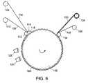
- FIG. 6shows a schematic view of a method for forming the differentially cured collimating film.
- FIG. 7shows a cross-sectional view of another embodiment.
- FIG. 8shows a perspective view of the embodiment in FIG. 7 .
- FIG. 9shows an embodiment of a logo pattern.
- FIG. 10shows a plot of a surface profile with an interference microscope trace which was made across the surface of a film made with the pattern transfer process.
- the inventionis directed to forming a pattern in a radiation curable material.
- the patternin one embodiment, is transparent when viewed in a direction substantially normal to the material. However, the pattern can be seen more clearly at a viewing angle of about fifteen degrees from the normal.
- FIG. 1illustrates an embodiment of the present invention for forming a pattern, such as exemplary pattern “ABC” provided by, for example, mask or pattern layer 10 , disposed between a radiation source 14 and a radiation curable material 12 .
- the mask layer 10can include polycarbonate, polyethylene, polybutylene or the like, and may include a low-tack adhesive.
- the curable material 12can include coatings and microstructured or patterned materials formulated from materials, such as polyester, urethane, or epoxy acrylates and methacrylates. Various additives including fillers, free-radical initiators and cationic initiators can be included in the material 12 to improve processing or performance. See, for example, Sartomer Company Bulletin Nos. 4018 or 4303, the teachings of which are incorporated by reference.
- the radiation source 14preferably provides actinic radiation, which causes photochemical activity in the curable material 12 . For example, typical ultraviolet light can be used.
- the pattern layer 10can include any kind of material that blocks at least a portion of the radiation from the radiation source to leave a similar pattern in the cured material 12 .
- the patterncan be formed by a colored pattern, such as, using common printing inks, printed on a transparent polymer film.
- the patterncan also be formed by embossing patterns that effect the transparency of the film.
- the patterncan be applied directly on either side of a substrate which carries the curable material 12 and after curing, the pattern may or may not be removed to leave the cured pattern in the cured layer 12 .
- the pattern layer 10can include a stencil or the like, such as a colored or semi-transparent film material or a clear resin with ultraviolet blocking chemical therein.
- the pattern layer 10has been removed but the pattern “ABC” has been transferred to the cured material 12 . It is believed that the pattern changes the curing rate of the material 12 to form the pattern in the cured material.
- the molecules in the formed patternare denser as the molecules have a longer time to cross-link than the molecules which do not have a mask thereover. These denser regions appear to have different indices of refraction.
- the patternis best viewed at an angle of about fifteen degrees.
- FIG. 3illustrates another embodiment for forming a pattern in a material.
- a pattern layer 10is positioned over a cured retroreflective structure 16 which can contain, for example, linear or cube-corner prisms.
- cured retroreflective structure 16can contain, for example, linear or cube-corner prisms. Examples of suitable cube-corner prisms are disclosed in U.S. Pat. No. 3,684,348, issued to Rowland on Aug. 15, 1972, the teachings of which are incorporated herein by reference.
- Moth-eye structures 18can be formed on the opposite side of the retroreflective structure 16 as shown in FIG. 3 . Moth-eye structures are explained in more detail in U.S. application Ser. No. 09/438,912, filed on Nov. 12, 1999, which corresponds to International Publication No. WO 01/35128, published on May 17, 2001. The teachings of each are incorporated herein in their entirety.
- the moth-eye structures 18are cured by the radiation source 14 through the pattern layer 10 such that the pattern is formed in the moth-eye structures 18 or diffusing structure or other suitable structures.
- a sub-wavelength structure appliedpreferably has an amplitude of about 0.4 microns and a period of less than about 0.3 microns.
- the structureis sinusoidal in appearance and can provide a deep green to deep blue color when viewed at grazing angles of incidence.
- the amplitudeis greater than two times the period to provide a two or greater to one aspect ratio.
- the structureis first produced on a photo resist-covered glass substrate by a holographic exposure using an ultraviolet laser.
- a suitable deviceis available from Holographic Lithography Systems of Bedford, Mass.
- An example of a methodis disclosed in U.S. Pat. No. 4,013,465, issued to Clapham et al. on Mar. 22, 1977, the teachings of which are incorporated herein by reference. This method is sensitive to any changes in the environment, such as temperature and dust, and care must taken.
- the structureis then transferred to a nickel shim by an electroforming process.
- a fine patterncan be formed on the mask layer 10 .
- the patterncan be a few tenths of a millimeter or less in width.
- a curable materialwhich is preferably substantially clear when cured, is formed on the opposite side of the mask layer 10 of the pattern and cured by a radiation source 14 . The fine pattern is thus transferred to the cured material.
- the mask layer 10is removed and the cured sheet is placed in front of a display, such as a liquid crystal display.
- the fine patternbreaks up the pixel pattern in the display without as much light loss as with diffuser sheets.
- the “photomask”can be clear or colored and be applied to either side of the carrier. If the curing radiation is highly collimated, it is desirable to have the “mask” be semi-transparent to allow for slow curing in that area. In cases where the radiation is less collimated, one can obtain cure through totally opaque masks via scattering and reflections into the masked area.
- the resulting productthen displays different optical behavior in areas that have been masked due to the variation in shrinkage and refractive index related to the speed of cure which is hindered by the “mask”.
- FIG. 4shows a perspective view of a typical collimating film 30 with linear prisms 32 having linear peaks 34 and valleys 36 .
- the dihedral angle of the first side 36 and second side 38 of the peak 34is typically ninety degrees. However, it can be a non-right angle.
- the linear prisms 32can be formed on a base film 40 .
- FIG. 5shows a perspective view of a prism array 52 of a differentially cured collimating film 50 .
- Many of the prisms which are not blocked by a mask, such as prism 54have a linear peak 56 .
- Many of the prisms, which are blocked, such as prism 58have a curved peak 60 .
- the curved peakis the result of curing through a mask which reduces or increases the cure rate with respect to the surrounding areas.
- curved peak 60is shaped compared to the normal apex of linear peak 56 of prism 58 .
- the region 62is curved in respect to another region which can result in a wider light distribution.
- the curved center line 66 of the peak in this prismcan be off center in respect to the normal center line 64 depending upon the curing mask used.
- This region 62also can have a slightly different index of refraction in respect to other areas.
- the prismscan be formed on a base film 68 , such as a polyester, polycarbonate, polyurethane, acrylic and polyvinyl chloride.
- the maskcan cover up to about fifty percent of the area of the product to be formed, such as a collimating film.
- the shape of the differential cure areacan be essentially any configuration or size. This allows one to tailor the light/distribution in specification areas of the sheet, such as to corners or edges, instead of the center of the sheet.
- the exposed portioncan result in raised portions or bumps.
- the structurecan have an appearance with recesses.
- the prismscan have nanometer size striations caused by the differential cure shrinkage pattern. These striations can perform like a vertical linear moth-eye structure. Some striations can extend from the peak to valley. The striation can range in width of between about 250 and 770 nanometers depending on the mask pattern. The striations can cause upward light tunneling.
- prismscan be used including cube-corner prisms.
- Cube-corner or prismatic retroreflectorsare described in U.S. Pat. No. 3,712,706, issued to Stamm on Jan. 23, 1973, the teachings of which are incorporated by reference herein.
- the prismsare made by forming a master negative die on a flat surface of a metal plate or other suitable material.
- To form the cube-cornersthree series of parallel equidistance intersecting V-shaped grooves sixty degrees apart are inscribed in the flat plate. The die is then used to process the desired cube-corner array into a rigid flat plastic surface. Further details concerning the structures and operation of cube-corner microprisms can be found in U.S. Pat. No.
- the pattern transfer conceptcan include forming a structured coating onto a smooth surface and also forming a pattern structure onto a micro optical array of any type including submicron to micron size surfaces. Further, a pattern can be placed on plano surfaces, prism surfaces, lens structures, and others. The pattern can be random, ordered or designed to convey a message.
- a mold 102is ruled with linear grooves 120 essentially parallel to the axis about which the mold rotates.
- the linear groovescan be pitched between about 0.05 and 0.2 mm (0.002 and 0.008 inches).
- a base film 104is unrolled from roll 106 .
- the base film 104can be a suitable material, such as a polyester.
- Mask film 108is unrolled from second roll 110 .
- Mask filmcan be formed of a suitable material, such as polyester, upon which a non-transparent design is printed on the transparent mask film.
- the non-transparent designcan be printed on the mask film in the same manner as a design is printed on an overhead transparency.
- base film 104 and mask film 108are pinched together by first pinch roller 112 against roller 102 .
- the base film 104 and mask filmare kept in close contact with mold 102 until second pinch roller 114 .
- base film and mask filmcan be laminated together as a single sheet and then unrolled from a single roll.
- a removable patterncan be directly printed on a first side of the base film with a suitable light blocking material, such as a water soluble ink or the like.
- a suitable light blocking materialsuch as a water soluble ink or the like.
- a curable layer of light curable materialis placed on the second side of the base film, and the curable layer is differentially cured in the presence of light directed through the pattern and base film to the curable layer.
- the removable patternis removed from the base film.
- itcan be removed with a solvent, such as water for a water soluble ink.
- other solventscan be used, such as alcohol, hydrocarbons, etc., depending upon the ink or other material used to form the light blocking pattern on the base film.
- Prism monomer material 116is placed at point 118 proximate to pinch roller 112 .
- the monomer materialsuch as an acrylic, flows into the grooves 120 of mold 102 .
- the prism monomer material 116is cured differentially by the partially blocked ultraviolet light as it passes ultraviolet lamps 122 , 124 , to form differentially cured collimating film 126 .
- Differentially cured collimating film 126is wound up on wind up roller 128 .
- the mask film 108is wound up on second wind up roller 130 .
- Lighter portionsinclude the regions with ninety degree linear prisms. Regions with darker portions include the prisms that were differentially cured by blocking by the mask. In these darker portions, the prisms are slightly distorted due to the different cure rate and appear darker because the light is spread over a broader range.
- a light directing film sheetingcan be used for collimating light in backlighting systems.
- the light directing film sheeting 200includes a base film 202 formed of a transparent polyester film, such as ICI Dupont 4000 PET, or polycarbonate, such as Rowland Technologies “Rowtec” film, having a thickness in the range of between about 50 and 250 micrometers (0.002 and 0.01 inches).
- the sheetingcan have a thickness in the range of between about 0.1 and 0.15 mm and (0.004 and 0.006 inches) and an index of refraction in the range of between about 1.49 and 1.59.
- a series of transparent linear prisms 204 having sides 206are formed over the base film 202 . Sides 206 can be isosceles.
- the linear prisms 204extend across the sheeting.
- the prismsare formed of a transparent resin, such as a mixture of polymerized CN104 polyacrylate available from Sartomer Chemical Co. and RDX51027 from UCB Chemical.
- the linear prismsare pitched a distance (p) in a range of between about 25 and 100 micrometers (0.001 and 0.004 inches), preferably about 48 micrometers (0.0019 inches) per prism.
- the linear prismshave a height (h) in a range of between about, 20 and 100 micrometers (0.0008 and 0.004 inches) preferably about 25 micrometers (0.001 inches).
- the linear prismshave pointed peaks 206 with a peak angle ( ⁇ ) as desired, with preferred values of 88 or 90 degrees in a sheeting. Base angles ⁇ 1 and ⁇ 2 can be the same or different.
- the linear prisms 204can be attached to the base film 202 by an optional prism adhesive layer 208 , such as 7650TC acrylic adhesive available from Bostik Chemical.
- Prism adhesive layer 208has a thickness (a 1 ) in the range of between about 2.5 and 12 micrometers (0.0001 and 0.0005 inches).
- a pattern structure 212is formed, such as with a resin composition similar to or the same as the prism side adhesive layer.
- the pattern structure 212can be attached to the base film 202 by pattern adhesive layer 214 , which is similar in material and thickness (a 2 ) to prism adhesive layer 208 .
- Pattern structure 212has a thickness in the range of between about 2.5 and 12 micrometers (0.0001 and 0.0005 inches).
- the pattern structure 230includes a logo 232 , which is an arrangement of four obtuse scalene triangles.
- the logocan be a company name, a trademark, a figure, or other desired design.
- the pattern structurecan be printed on sheeting such as a polyester overhead projector sheeting by a laser printer.
- the logois repeated in a line on a first axis about every 13 mm.
- the logos in each lineare off-set in the next by a half of a logo and the lines repeat about every 7.5 mm along a second axis in the run/web direction, which is perpendicular to the first axis.
- the lines of the logoare about 0.5 mm in width.
- Other types of designsinclude cross hatching, geometric figures, numerals, letters, etc.
- the linesare depressions 216 or recesses in the surface of the non-prism side.
- Depressions 216can have a depth (d) in the range of between about 0.3 and 2.0 micrometers with an average depth of one micrometer.
- the depressionsare not uniform in slope from edges 218 to low point 220 .
- the depressionscan have an average slope of 0.5 degrees to the surface of the base film 102 with the slope being as high as one degree.
- the pattern structureis formed by placing a mask film temporarily on one side of the base film.
- the mask filmhas a logo, geometric form (lines, circles, curves, etc.), alphanumerics or any other desired design formed thereon that can block a portion of the ultraviolet light as it passes from ultraviolet light source through the mask film to the base film.
- the portion of the mask film without the logo printed thereonis more transparent to ultraviolet light.
- an adhesive layeris deposited and an uncured radiation curable resin is placed on the adhesive layer.
- Ultraviolet lightis directed from an ultraviolet light source through the mask layer through the base layer through the adhesive layer to the resin layer.
- the resin layeris differentially cured because the ultraviolet light intensity is blocked unevenly by the printed patterned to the resin layer resulting in the pattern structure.
- the pattern structureis uneven and segmented.
- the portions of the resin layer that have the greatest blockage from the ultraviolet lighthave the deepest depressions into the surface.
- the portions that were exposed to ultraviolet lightresulted in segments with relatively flat surfaces.
- the mask filmis then removed from the base film.
- the linear prismsare cast on the same side of the base film where the mask film had been placed.
- the linear prismsare cured by ultraviolet light directed through the base film.
- the linear prismscan be slightly differently cured in the portions that are exposed to the ultraviolet light that passes through the pattern structure that is uneven and segmented.
- the filmcan be placed between a light guide and a display, such as a liquid crystal display.
- a displaysuch as a liquid crystal display.
- the fine patternbreaks-up the pixel pattern in the display without as much light loss as with a diffuser sheet.
- the pattern structure on the filmcan be readily visible across the film.
- the filmcan be used as a single sheet or as a two-sheet or more system.
- a two-sheet systemhas the linear prisms peaks pointed in the same direction and the length of the peaks on each sheet are often crossed at ninety degrees.
- Linear prismswere cast on polycarbonate and covered with a number 30LC mask film (manufactured by Ivex Packaging Corporation) that had a blue colored “PEEL” pattern printed on it.
- Moth-eye structureswere cast on the opposite side of the prisms and cured by ultraviolet radiation at a web speed of about twelve meters per minute (forty feet per minute) past two 157-236 watts/lineal centimeter (400-600 Watts/lineal inch) ultraviolet lamps manufactured by Eye Ultraviolet Corporation. After removing the mask film, the cured moth-eye structures retained the “PEEL” pattern which could not be readily seen at a zero degree viewing angle but were pronounced at about a fifteen degree viewing angle.
- Alphanumeric imageswere handwritten onto the surface of a mask film on a cling mask sample of polycarbonate film manufactured by Rowland Technologies Incorporated. Commonly available felt tip marker pens were used to form the images.
- An ultraviolet curable coating of epoxy acrylatewas applied to the other side of the polycarbonate film and cured under a 236 Watts per lineal centimeter (600 Watts per lineal) inch lamp at about 4.6 meters per minute (fifteen feet per minute). The mask film was removed and the cured coating was visually examined at various angles. The images that had been on the mask film were visible at shallow viewing angles in the cured coating.
- FIG. 10shows a plot of a surface profile with an interference microscope trace which was made across the surface of a film made with the pattern transfer process.
- the height of the featuresis slightly less than one wavelength of red light.
- Red light wavelengthis 632.8 nm (2.49 ⁇ 10 ⁇ 5 inches).
- the height of the featuresis approximately 500 to 900 nm (1.9685 ⁇ 10 ⁇ 5 to 3.5433 ⁇ 10 ⁇ 5 inches).
- the average heightis about 640 nm (2.5197 ⁇ 10 ⁇ 5 inches).
- the height and slope of the featurescaused some light deviation as the light passes through the film. However, the effect on brightness appears to be positive by about a one percent gain. Additionally, these features can act as resting points for the prism peaks of collimating films as the films are stacked upon each other and therefore prevent the majority of the prism peaks from being damaged by abrasion.
Landscapes
- Physics & Mathematics (AREA)
- Health & Medical Sciences (AREA)
- Engineering & Computer Science (AREA)
- General Physics & Mathematics (AREA)
- Toxicology (AREA)
- Thermal Sciences (AREA)
- Oral & Maxillofacial Surgery (AREA)
- Mechanical Engineering (AREA)
- Ophthalmology & Optometry (AREA)
- Manufacturing & Machinery (AREA)
- Optics & Photonics (AREA)
- Laminated Bodies (AREA)
- Optical Elements Other Than Lenses (AREA)
- Credit Cards Or The Like (AREA)
- Manufacturing Of Printed Wiring (AREA)
- Application Of Or Painting With Fluid Materials (AREA)
- Heating, Cooling, Or Curing Plastics Or The Like In General (AREA)
Abstract
Description
Claims (8)
Priority Applications (1)
| Application Number | Priority Date | Filing Date | Title |
|---|---|---|---|
| US11/881,270US7517205B2 (en) | 2000-08-18 | 2007-07-26 | Differentially cured materials and process for forming same |
Applications Claiming Priority (4)
| Application Number | Priority Date | Filing Date | Title |
|---|---|---|---|
| US22669700P | 2000-08-18 | 2000-08-18 | |
| US25617600P | 2000-12-15 | 2000-12-15 | |
| US09/928,247US7250122B2 (en) | 2000-08-18 | 2001-08-10 | Differentially cured materials and process for forming same |
| US11/881,270US7517205B2 (en) | 2000-08-18 | 2007-07-26 | Differentially cured materials and process for forming same |
Related Parent Applications (1)
| Application Number | Title | Priority Date | Filing Date |
|---|---|---|---|
| US09/928,247ContinuationUS7250122B2 (en) | 2000-08-18 | 2001-08-10 | Differentially cured materials and process for forming same |
Publications (2)
| Publication Number | Publication Date |
|---|---|
| US20070292549A1 US20070292549A1 (en) | 2007-12-20 |
| US7517205B2true US7517205B2 (en) | 2009-04-14 |
Family
ID=26920792
Family Applications (2)
| Application Number | Title | Priority Date | Filing Date |
|---|---|---|---|
| US09/928,247Expired - Fee RelatedUS7250122B2 (en) | 2000-08-18 | 2001-08-10 | Differentially cured materials and process for forming same |
| US11/881,270Expired - Fee RelatedUS7517205B2 (en) | 2000-08-18 | 2007-07-26 | Differentially cured materials and process for forming same |
Family Applications Before (1)
| Application Number | Title | Priority Date | Filing Date |
|---|---|---|---|
| US09/928,247Expired - Fee RelatedUS7250122B2 (en) | 2000-08-18 | 2001-08-10 | Differentially cured materials and process for forming same |
Country Status (9)
| Country | Link |
|---|---|
| US (2) | US7250122B2 (en) |
| EP (1) | EP1309437B1 (en) |
| JP (1) | JP2004506547A (en) |
| KR (1) | KR100798172B1 (en) |
| CN (1) | CN100389017C (en) |
| AU (1) | AU2001284844A1 (en) |
| DE (1) | DE60117573T2 (en) |
| TW (1) | TWI294821B (en) |
| WO (1) | WO2002016106A2 (en) |
Cited By (4)
| Publication number | Priority date | Publication date | Assignee | Title |
|---|---|---|---|---|
| US20130082458A1 (en)* | 2008-04-08 | 2013-04-04 | Lily O'Boyle | Ovd containing device |
| EP2715414A4 (en)* | 2011-05-31 | 2014-12-31 | 3M Innovative Properties Co | CUBIC CORNER COATING HAVING AN OPTICALLY VARIABLE MARKING |
| US9415539B2 (en) | 2011-05-31 | 2016-08-16 | 3M Innovative Properties Company | Method for making microstructured tools having discontinuous topographies, and articles produced therefrom |
| US9523919B2 (en) | 2011-05-31 | 2016-12-20 | 3M Innovative Properties Company | Methods for making differentially pattern cured microstructured articles |
Families Citing this family (34)
| Publication number | Priority date | Publication date | Assignee | Title |
|---|---|---|---|---|
| US7313253B2 (en)* | 1998-09-11 | 2007-12-25 | Digimarc Corporation | Methods and tangible objects employing machine readable data in photo-reactive materials |
| US20040190102A1 (en)* | 2000-08-18 | 2004-09-30 | Mullen Patrick W. | Differentially-cured materials and process for forming same |
| EP1309437B1 (en) | 2000-08-18 | 2006-03-01 | Reflexite Corporation | Differentially cured materials and process for forming same |
| US7230764B2 (en)* | 2000-08-18 | 2007-06-12 | Reflexite Corporation | Differentially-cured materials and process for forming same |
| EP1625430A2 (en) | 2003-05-02 | 2006-02-15 | Reflexite Corporation | Light-redirecting optical structures |
| US8181884B2 (en)* | 2003-11-17 | 2012-05-22 | Digimarc Corporation | Machine-readable features for objects |
| WO2005056275A1 (en)* | 2003-12-15 | 2005-06-23 | Multi Sign A/S | System and method for the manufacture of a film comprising a retro reflective pattern |
| EA011968B1 (en)† | 2004-04-30 | 2009-06-30 | Де Ля Рю Интернэшнл Лимитед | Security devices |
| GB0427607D0 (en)* | 2004-12-16 | 2005-01-19 | Microsharp Corp Ltd | Structured optical film |
| CN101171536B (en)* | 2005-03-09 | 2010-12-01 | 3M创新有限公司 | Microreplicated article with defect-reducing surface |
| DE102005060731A1 (en)* | 2005-12-16 | 2007-06-21 | Röhm Gmbh | Prism films for optical applications |
| DE102006011949A1 (en)* | 2006-03-15 | 2007-09-20 | Epg (Engineered Nanoproducts Germany) Ag | Process for the production of defect-free microoptical light guide elements of large width |
| JP4006650B1 (en)* | 2006-05-08 | 2007-11-14 | ソニー株式会社 | Optical film, method for producing the same, and display device |
| DE102006029852A1 (en)† | 2006-06-27 | 2008-01-03 | Giesecke & Devrient Gmbh | Method of applying a microstructure, mold and microstructured article |
| JP5288753B2 (en)* | 2007-09-07 | 2013-09-11 | 新光電気工業株式会社 | Method and apparatus for laminating UV curable waveguide material |
| CN106154399A (en)* | 2008-04-02 | 2016-11-23 | 3M创新有限公司 | Light directing film and preparation method thereof |
| EP2120070B1 (en)* | 2008-05-16 | 2014-03-12 | LG Electronics Inc. | Optical sheet, backlight unit, and liquid crystal display |
| TW201017280A (en)* | 2008-10-28 | 2010-05-01 | Shiang-Lin Liao | Substrate-free optical film |
| KR101595925B1 (en)* | 2008-12-31 | 2016-02-22 | 미래나노텍(주) | Mold, method and apparatus for manufacturing optical member |
| WO2010100902A1 (en)* | 2009-03-03 | 2010-09-10 | 三菱レイヨン株式会社 | Process for producing film |
| US20100237539A1 (en)* | 2009-03-20 | 2010-09-23 | Chang-Chih Sung | Manufacturing method and apparatus for optical sheet |
| KR200454030Y1 (en)* | 2009-04-20 | 2011-06-10 | 대명조명주식회사 | Ceiling landfill with easy separation, bonding and decoration |
| JP4856785B2 (en)* | 2010-04-09 | 2012-01-18 | 三菱レイヨン株式会社 | Manufacturing method and manufacturing apparatus for article having fine uneven structure on surface |
| CN102441989A (en)* | 2010-09-17 | 2012-05-09 | 索尼公司 | Manufacturing method of laminated body, stamper, transfer device, laminated body, molding element and optical element |
| JP6252047B2 (en)* | 2013-09-03 | 2017-12-27 | 大日本印刷株式会社 | Transmittance anisotropic member, method for manufacturing transmittance anisotropic member, and display device |
| CN106226849B (en)* | 2014-08-26 | 2019-03-01 | 友辉光电股份有限公司 | Method for forming concave-convex structure on substrate and method for forming optical film |
| CN107206758A (en)* | 2015-01-16 | 2017-09-26 | 博优国际集团公司 | Mulch and method for making mulch |
| CN106646716A (en)* | 2017-02-14 | 2017-05-10 | 山西大学 | Space stacking light beam distributed phase delayer and speckle elimination method thereof |
| US11499321B2 (en) | 2017-07-13 | 2022-11-15 | Beaulieu International Group Nv | Covering and method for producing coverings |
| NL2023024B1 (en)* | 2019-04-29 | 2020-11-05 | Veko Lightsystems Int B V | Thin-walled optical element lens for a light source provided with prismatic structures on both sides. |
| US11392810B2 (en)* | 2019-12-12 | 2022-07-19 | Thales Dis France Sa | Covert floating image |
| US11981097B1 (en) | 2020-01-10 | 2024-05-14 | Apple Inc. | Pattern printing on prisms |
| US20230372424A1 (en) | 2020-10-01 | 2023-11-23 | Novid 20 Ltd | Antiviral active cinnamon extract and process |
| US11124932B1 (en)* | 2021-04-30 | 2021-09-21 | Mark Joseph O'Neill | Retroreflective traffic stripe for both dry and wet weather conditions |
Citations (113)
| Publication number | Priority date | Publication date | Assignee | Title |
|---|---|---|---|---|
| US1241886A (en) | 1916-07-12 | 1917-10-02 | Levi Leroy Rowe | Lens. |
| US2248638A (en) | 1937-02-22 | 1941-07-08 | Merton Thomas Ralph | Sheet material with prismatic surfaces |
| US2310790A (en) | 1943-02-09 | Optical reflecting material | ||
| US2380447A (en) | 1945-07-31 | Optical reflecting material | ||
| US2474317A (en) | 1949-06-28 | Light refracting and transmitting | ||
| US2904674A (en) | 1956-11-29 | 1959-09-15 | Bell Telephone Labor Inc | Radiant energy highway communication system with controlled directive antenna |
| US3670260A (en) | 1970-05-15 | 1972-06-13 | American Optical Corp | Controlled optical beam forming device |
| US3684348A (en) | 1970-09-29 | 1972-08-15 | Rowland Dev Corp | Retroreflective material |
| US3712706A (en) | 1971-01-04 | 1973-01-23 | American Cyanamid Co | Retroreflective surface |
| US3718078A (en) | 1970-12-31 | 1973-02-27 | Polaroid Corp | Smoothly granulated optical surface and method for making same |
| US3853578A (en) | 1972-09-08 | 1974-12-10 | Senri Kikaku Sogo Kk | Method of manufacturing decorative boards with depression patterns |
| US4013465A (en) | 1973-05-10 | 1977-03-22 | Secretary Of State For Defence In Her Britannic Majesty's Government Of The United Kingdom Of Great Britain And Northern Ireland | Reducing the reflectance of surfaces to radiation |
| US4064433A (en) | 1976-06-30 | 1977-12-20 | K-S-H, Inc. | Prismatic lighting panel |
| US4154219A (en) | 1977-03-11 | 1979-05-15 | E-Systems, Inc. | Prismatic solar reflector apparatus and method of solar tracking |
| US4242723A (en) | 1979-05-14 | 1980-12-30 | Keene Corporation | Low level work area lighting system |
| US4260220A (en) | 1979-06-15 | 1981-04-07 | Canadian Patents And Development Limited | Prism light guide having surfaces which are in octature |
| US4374077A (en) | 1980-02-01 | 1983-02-15 | Minnesota Mining And Manufacturing Company | Process for making information carrying discs |
| US4402571A (en) | 1981-02-17 | 1983-09-06 | Polaroid Corporation | Method for producing a surface relief pattern |
| US4469407A (en) | 1982-02-08 | 1984-09-04 | Polaroid Corporation | Laser apodizing filter |
| US4477529A (en) | 1983-12-29 | 1984-10-16 | General Electric Company | Photocurable polyfunctional acrylic coating and decorative articles coated therewith |
| US4485123A (en) | 1982-02-12 | 1984-11-27 | Union Carbide Corporation | Process for producing textured coatings |
| US4496216A (en) | 1982-12-30 | 1985-01-29 | Polaroid Corporation | Method and apparatus for exposing photosensitive material |
| US4514345A (en) | 1983-08-23 | 1985-04-30 | The Procter & Gamble Company | Method of making a foraminous member |
| US4542449A (en) | 1983-08-29 | 1985-09-17 | Canadian Patents & Development Limited | Lighting panel with opposed 45° corrugations |
| US4576850A (en) | 1978-07-20 | 1986-03-18 | Minnesota Mining And Manufacturing Company | Shaped plastic articles having replicated microstructure surfaces |
| US4732715A (en) | 1985-09-20 | 1988-03-22 | Bausch & Lomb Incorporated | Manufacture of polymeric contact lenses |
| US4791540A (en) | 1987-05-26 | 1988-12-13 | Minnesota Mining And Manufacturing Company | Light fixture providing normalized output |
| US4839250A (en) | 1987-08-10 | 1989-06-13 | Polaroid Corporation, Patent Department | Method of replicating volume phase reflection holograms |
| US4874213A (en) | 1987-08-10 | 1989-10-17 | Polaroid Corporation | Method of forming volume phase reflection holograms |
| US4874228A (en) | 1987-03-24 | 1989-10-17 | Minnesota Mining And Manufacturing Company | Back-lit display |
| US4883341A (en) | 1987-04-24 | 1989-11-28 | Tir Systems Ltd | Non-reflective graphic surface |
| US4888260A (en) | 1987-08-10 | 1989-12-19 | Polaroid Corporation | Volume phase reflection holograms and methods for fabricating them |
| US4906070A (en) | 1985-11-21 | 1990-03-06 | Minnesota Mining And Manufacturing Company | Totally internally reflecting thin, flexible film |
| US4937716A (en) | 1988-05-05 | 1990-06-26 | Tir Systems Ltd | Illuminating device having non-absorptive variable transmissivity cover |
| US4942112A (en) | 1988-01-15 | 1990-07-17 | E. I. Du Pont De Nemours And Company | Photopolymerizable compositions and elements for refractive index imaging |
| US4984144A (en) | 1987-05-08 | 1991-01-08 | Minnesota Mining And Manufacturing Company | High aspect ratio light fixture and film for use therein |
| US4999234A (en) | 1987-08-10 | 1991-03-12 | Polaroid Corporation | Holographic optical data storage medium |
| US5005108A (en) | 1989-02-10 | 1991-04-02 | Lumitex, Inc. | Thin panel illuminator |
| US5015524A (en) | 1988-12-27 | 1991-05-14 | Mitsubishi Rayon Company, Ltd. | Lens sheet |
| US5056892A (en) | 1985-11-21 | 1991-10-15 | Minnesota Mining And Manufacturing Company | Totally internally reflecting thin, flexible film |
| US5093765A (en) | 1990-02-16 | 1992-03-03 | Tosoh Corporation | Back lighting device for a panel |
| US5126882A (en) | 1987-11-12 | 1992-06-30 | Mitsubishi Rayon Co., Ltd. | Plane light source unit |
| US5161041A (en) | 1990-04-26 | 1992-11-03 | Ois Optical Imaging Systems, Inc. | Lighting assembly for a backlit electronic display including an integral image splitting and collimating means |
| US5175030A (en) | 1989-02-10 | 1992-12-29 | Minnesota Mining And Manufacturing Company | Microstructure-bearing composite plastic articles and method of making |
| US5183597A (en) | 1989-02-10 | 1993-02-02 | Minnesota Mining And Manufacturing Company | Method of molding microstructure bearing composite plastic articles |
| US5186530A (en) | 1991-11-22 | 1993-02-16 | Tir Systems, Ltd. | Lighting structure having variable transmissivity internal light guide illumination |
| US5190370A (en) | 1991-08-21 | 1993-03-02 | Minnesota Mining And Manufacturing Company | High aspect ratio lighting element |
| US5267062A (en) | 1991-08-26 | 1993-11-30 | Rockwell International Corporation | System for backlighting LCD matrices including luminescent dots each followed by and at the focal point of a lens |
| US5281371A (en)* | 1990-11-16 | 1994-01-25 | Canon Kabushiki Kaisha | Method and apparatus for forming substrate sheet for optical recording medium |
| US5289351A (en) | 1991-03-22 | 1994-02-22 | Tosoh Corporation | Backlighting device |
| US5394255A (en) | 1992-01-27 | 1995-02-28 | Sekisui Kagaku Kogyo Kabushiki Kaisha | Liquid crystal display using a plurality of light adjusting sheets angled at 5 degrees or more |
| US5396350A (en) | 1993-11-05 | 1995-03-07 | Alliedsignal Inc. | Backlighting apparatus employing an array of microprisms |
| US5435816A (en)* | 1993-01-14 | 1995-07-25 | Minnesota Mining And Manufacturing Company | Method of making an abrasive article |
| US5442523A (en) | 1991-08-22 | 1995-08-15 | Tosoh Corporation | Backlighting device |
| US5480596A (en)* | 1989-07-12 | 1996-01-02 | Canon Kabushiki Kaisha | Optical recording medium substrate sheet producing apparatus having roll stamper with elastomer layer of predetermined hardness |
| US5521797A (en) | 1993-02-01 | 1996-05-28 | Tosoh Corporation | Backlighting device |
| JPH08137375A (en) | 1994-11-02 | 1996-05-31 | Toppan Printing Co Ltd | Relief image forming material and relief image forming method |
| US5550676A (en) | 1990-09-12 | 1996-08-27 | Mitsubishi Rayon Co., Ltd | Surface light source element |
| US5565151A (en) | 1994-09-28 | 1996-10-15 | Reflexite Corporation | Retroreflective prism structure with windows formed thereon |
| US5579134A (en) | 1994-11-30 | 1996-11-26 | Honeywell Inc. | Prismatic refracting optical array for liquid flat panel crystal display backlight |
| US5592332A (en) | 1992-12-25 | 1997-01-07 | Dai Nippon Printing Co., Ltd. | Renticular lens, surface light source, and liquid crystal display apparatus |
| US5598280A (en) | 1993-03-23 | 1997-01-28 | Dai Nippon Printing Co., Ltd. | Film lens and a surface light source using the same |
| US5600462A (en) | 1992-09-16 | 1997-02-04 | International Business Machines Corporation | Optical film and liquid crystal display device using the film |
| US5629784A (en) | 1994-04-12 | 1997-05-13 | Ois Optical Imaging Systems, Inc. | Liquid crystal display with holographic diffuser and prism sheet on viewer side |
| US5635278A (en) | 1995-02-03 | 1997-06-03 | Minnesota Mining And Manufacturing Company | Scratch resistant optical films and method for producing same |
| WO1997030604A1 (en) | 1996-02-20 | 1997-08-28 | Scapa Group Plc | Tobacco conveyor belt |
| US5670096A (en) | 1990-11-15 | 1997-09-23 | Minnesota Mining And Manufacturing Company | Retroreflective article comprising a transparent base sheet and nacreous pigment coating, method for making such a base sheet, and method for making a forming master |
| US5711589A (en) | 1993-06-22 | 1998-01-27 | Mitsubishi Rayon Co., Ltd. | Plane light source unit |
| US5721603A (en) | 1993-01-11 | 1998-02-24 | U.S. Philips Corporation | Illumination system and display device including such a system |
| US5724108A (en) | 1994-03-14 | 1998-03-03 | Hitachi, Ltd. | Liquid crystal display device with a prism sheet that increases brightness in the optimum range of viewing angle |
| US5771328A (en) | 1995-03-03 | 1998-06-23 | Minnesota Mining And Manufacturing Company | Light directing film having variable height structured surface and light directing article constructed therefrom |
| US5769522A (en) | 1991-09-09 | 1998-06-23 | Enplas Corporation | Surface light source device |
| US5780140A (en) | 1996-09-23 | 1998-07-14 | Reflexite Corporation | Retroreflective microprismatic material with top face curvature and method of making same |
| US5816677A (en) | 1905-03-01 | 1998-10-06 | Canon Kabushiki Kaisha | Backlight device for display apparatus |
| US5838403A (en) | 1996-02-14 | 1998-11-17 | Physical Optics Corporation | Liquid crystal display system with internally reflecting waveguide for backlighting and non-Lambertian diffusing |
| US5844720A (en) | 1995-09-08 | 1998-12-01 | Goyo Paper Working Co., Ltd. | Prism sheet |
| US5851062A (en) | 1995-08-11 | 1998-12-22 | Omron Corporation | Prism sheet for surface light source |
| US5857561A (en) | 1995-09-14 | 1999-01-12 | Scapa Group Plc | Tobacco conveyor belt |
| US5863113A (en) | 1993-06-22 | 1999-01-26 | Mitsubishi Rayon Co., Ltd. | Plane light source unit |
| US5909083A (en)* | 1996-02-16 | 1999-06-01 | Dai Nippon Printing Co., Ltd. | Process for producing plasma display panel |
| WO1999028468A1 (en) | 1997-12-02 | 1999-06-10 | The Regents Of The University Of California | Modulating b lymphocyte chemokine/receptor interactions |
| US5917664A (en) | 1996-02-05 | 1999-06-29 | 3M Innovative Properties Company | Brightness enhancement film with soft cutoff |
| US5919551A (en) | 1996-04-12 | 1999-07-06 | 3M Innovative Properties Company | Variable pitch structured optical film |
| US5932626A (en) | 1997-05-09 | 1999-08-03 | Minnesota Mining And Manufacturing Company | Optical product prepared from high index of refraction brominated monomers |
| WO1999042861A1 (en) | 1998-02-18 | 1999-08-26 | Minnesota Mining And Manufacturing Company | Optical film |
| US5946991A (en) | 1997-09-03 | 1999-09-07 | 3M Innovative Properties Company | Method for knurling a workpiece |
| US5995690A (en) | 1996-11-21 | 1999-11-30 | Minnesota Mining And Manufacturing Company | Front light extraction film for light guiding systems and method of manufacture |
| US6052164A (en) | 1993-03-01 | 2000-04-18 | 3M Innovative Properties Company | Electroluminescent display with brightness enhancement |
| US6075649A (en) | 1998-04-22 | 2000-06-13 | Dai Nippon Printing Co., Ltd. | Lens film and planar light source apparatus |
| JP2000210963A (en) | 1999-01-26 | 2000-08-02 | Mitsubishi Heavy Ind Ltd | Energy beam emitting type continuously molding machine and fiber-reinforced plastic plate-like molding |
| US6114010A (en) | 1995-02-03 | 2000-09-05 | 3M Innovative Properties Company | Devices with flame retardant ultraviolet cured multi-layered film |
| US6147804A (en) | 1997-04-22 | 2000-11-14 | Dai Nippon Printing Co., Ltd. | Optical sheet lamination |
| US6164782A (en) | 1994-10-04 | 2000-12-26 | 3M Innovative Property Company | Self-contained lighted marking device |
| WO2001027527A1 (en) | 1999-10-08 | 2001-04-19 | 3M Innovative Properties Company | Optical element having programmed optical structures |
| WO2001035128A2 (en) | 1999-11-12 | 2001-05-17 | Reflexite Corporation | Subwavelength optical microstructure light collimating films |
| US6239851B1 (en) | 1995-10-12 | 2001-05-29 | Ibm Corporation | Planar light source device having polarization separator formed of two sheets with mating triangular prisms and different indices of refraction |
| US6277471B1 (en) | 1999-06-18 | 2001-08-21 | Shih Chieh Tang | Brightness enhancement film |
| US6280063B1 (en) | 1997-05-09 | 2001-08-28 | 3M Innovative Properties Company | Brightness enhancement article |
| US6322236B1 (en) | 1999-02-09 | 2001-11-27 | 3M Innovative Properties Company | Optical film with defect-reducing surface and method for making same |
| WO2002004858A2 (en) | 2000-07-11 | 2002-01-17 | 3M Innovative Properties Company | Backlight with structured sufaces |
| US6356389B1 (en) | 1999-11-12 | 2002-03-12 | Reflexite Corporation | Subwavelength optical microstructure light collimating films |
| US6356674B1 (en) | 1994-01-21 | 2002-03-12 | Sharp Kabushiki Kaisha | Electrically controllable grating, and optical elements having an electrically controllable grating |
| US6357888B1 (en) | 1998-09-24 | 2002-03-19 | Sharp Kabushiki Kaisha | Surface illuminant device emitting light in multiple directions in concentrative manner |
| US6359735B1 (en) | 1997-03-04 | 2002-03-19 | Fraunhofer Gesellschaft Zur Forderung Der Angewandten Forschung E.V. | Antireflective coating and method of manufacturing same |
| US20020051866A1 (en) | 2000-08-18 | 2002-05-02 | Reflexite Corporation | Differentially cured materials and process for forming same |
| WO2002034514A1 (en) | 2000-10-27 | 2002-05-02 | 3M Innovative Properties Company | Method and materials for preventing warping in optical films |
| US20020057497A1 (en) | 1999-10-08 | 2002-05-16 | 3M Innovative Properties Company | Optical film with variable angle prisms |
| WO2003046617A1 (en) | 2001-11-28 | 2003-06-05 | Saint-Gobain Glass France | Textured transparent plate with high light transmission |
| US6576887B2 (en) | 2001-08-15 | 2003-06-10 | 3M Innovative Properties Company | Light guide for use with backlit display |
| US6588883B2 (en) | 2001-01-15 | 2003-07-08 | Matsushita Electric Industrial Co., Ltd. | Liquid injector, method of manufacturing the injector, and ink-jet spray using the injector |
| US20030214728A1 (en) | 2002-05-20 | 2003-11-20 | General Electric Company | Optical substrate and method of making |
| US6787202B2 (en) | 2000-02-10 | 2004-09-07 | Teijin Limited | Polyester film composite, light-diffuser plate and utilization thereof |
| US6827456B2 (en) | 1999-02-23 | 2004-12-07 | Solid State Opto Limited | Transreflectors, transreflector systems and displays and methods of making transreflectors |
Family Cites Families (5)
| Publication number | Priority date | Publication date | Assignee | Title |
|---|---|---|---|---|
| US214728A (en)* | 1879-04-22 | Improvement in fruit-driers | ||
| US135128A (en)* | 1873-01-21 | Improvement in traction or portable engines | ||
| US2904673A (en) | 1957-02-13 | 1959-09-15 | Sr Edwin F Guth | Light diffusors for illuminating devices |
| US3046617A (en)* | 1959-01-23 | 1962-07-31 | Grayboff Marilyn | Light-transmitting structural panel |
| US5616069A (en)* | 1995-12-19 | 1997-04-01 | Micron Technology, Inc. | Directional spray pad scrubber |
- 2001
- 2001-08-10EPEP01963933Apatent/EP1309437B1/ennot_activeExpired - Lifetime
- 2001-08-10USUS09/928,247patent/US7250122B2/ennot_activeExpired - Fee Related
- 2001-08-10JPJP2002521010Apatent/JP2004506547A/ennot_activeWithdrawn
- 2001-08-10CNCNB018145361Apatent/CN100389017C/ennot_activeExpired - Fee Related
- 2001-08-10DEDE60117573Tpatent/DE60117573T2/ennot_activeExpired - Lifetime
- 2001-08-10KRKR1020037002376Apatent/KR100798172B1/ennot_activeExpired - Fee Related
- 2001-08-10WOPCT/US2001/025241patent/WO2002016106A2/enactiveIP Right Grant
- 2001-08-10AUAU2001284844Apatent/AU2001284844A1/ennot_activeAbandoned
- 2001-08-14TWTW090119893Apatent/TWI294821B/ennot_activeIP Right Cessation
- 2007
- 2007-07-26USUS11/881,270patent/US7517205B2/ennot_activeExpired - Fee Related
Patent Citations (121)
| Publication number | Priority date | Publication date | Assignee | Title |
|---|---|---|---|---|
| US2310790A (en) | 1943-02-09 | Optical reflecting material | ||
| US2380447A (en) | 1945-07-31 | Optical reflecting material | ||
| US2474317A (en) | 1949-06-28 | Light refracting and transmitting | ||
| US5816677A (en) | 1905-03-01 | 1998-10-06 | Canon Kabushiki Kaisha | Backlight device for display apparatus |
| US1241886A (en) | 1916-07-12 | 1917-10-02 | Levi Leroy Rowe | Lens. |
| US2248638A (en) | 1937-02-22 | 1941-07-08 | Merton Thomas Ralph | Sheet material with prismatic surfaces |
| US2904674A (en) | 1956-11-29 | 1959-09-15 | Bell Telephone Labor Inc | Radiant energy highway communication system with controlled directive antenna |
| US3670260A (en) | 1970-05-15 | 1972-06-13 | American Optical Corp | Controlled optical beam forming device |
| US3684348A (en) | 1970-09-29 | 1972-08-15 | Rowland Dev Corp | Retroreflective material |
| US3718078A (en) | 1970-12-31 | 1973-02-27 | Polaroid Corp | Smoothly granulated optical surface and method for making same |
| US3712706A (en) | 1971-01-04 | 1973-01-23 | American Cyanamid Co | Retroreflective surface |
| US3853578A (en) | 1972-09-08 | 1974-12-10 | Senri Kikaku Sogo Kk | Method of manufacturing decorative boards with depression patterns |
| US4013465A (en) | 1973-05-10 | 1977-03-22 | Secretary Of State For Defence In Her Britannic Majesty's Government Of The United Kingdom Of Great Britain And Northern Ireland | Reducing the reflectance of surfaces to radiation |
| US4064433A (en) | 1976-06-30 | 1977-12-20 | K-S-H, Inc. | Prismatic lighting panel |
| US4154219A (en) | 1977-03-11 | 1979-05-15 | E-Systems, Inc. | Prismatic solar reflector apparatus and method of solar tracking |
| US4576850A (en) | 1978-07-20 | 1986-03-18 | Minnesota Mining And Manufacturing Company | Shaped plastic articles having replicated microstructure surfaces |
| US4242723A (en) | 1979-05-14 | 1980-12-30 | Keene Corporation | Low level work area lighting system |
| US4260220A (en) | 1979-06-15 | 1981-04-07 | Canadian Patents And Development Limited | Prism light guide having surfaces which are in octature |
| US4374077A (en) | 1980-02-01 | 1983-02-15 | Minnesota Mining And Manufacturing Company | Process for making information carrying discs |
| US4402571A (en) | 1981-02-17 | 1983-09-06 | Polaroid Corporation | Method for producing a surface relief pattern |
| US4469407A (en) | 1982-02-08 | 1984-09-04 | Polaroid Corporation | Laser apodizing filter |
| US4485123A (en) | 1982-02-12 | 1984-11-27 | Union Carbide Corporation | Process for producing textured coatings |
| US4496216A (en) | 1982-12-30 | 1985-01-29 | Polaroid Corporation | Method and apparatus for exposing photosensitive material |
| US4514345A (en) | 1983-08-23 | 1985-04-30 | The Procter & Gamble Company | Method of making a foraminous member |
| US4542449A (en) | 1983-08-29 | 1985-09-17 | Canadian Patents & Development Limited | Lighting panel with opposed 45° corrugations |
| US4477529A (en) | 1983-12-29 | 1984-10-16 | General Electric Company | Photocurable polyfunctional acrylic coating and decorative articles coated therewith |
| US4732715A (en) | 1985-09-20 | 1988-03-22 | Bausch & Lomb Incorporated | Manufacture of polymeric contact lenses |
| US5056892A (en) | 1985-11-21 | 1991-10-15 | Minnesota Mining And Manufacturing Company | Totally internally reflecting thin, flexible film |
| US4906070A (en) | 1985-11-21 | 1990-03-06 | Minnesota Mining And Manufacturing Company | Totally internally reflecting thin, flexible film |
| US4874228A (en) | 1987-03-24 | 1989-10-17 | Minnesota Mining And Manufacturing Company | Back-lit display |
| US4883341A (en) | 1987-04-24 | 1989-11-28 | Tir Systems Ltd | Non-reflective graphic surface |
| US4984144A (en) | 1987-05-08 | 1991-01-08 | Minnesota Mining And Manufacturing Company | High aspect ratio light fixture and film for use therein |
| US4791540A (en) | 1987-05-26 | 1988-12-13 | Minnesota Mining And Manufacturing Company | Light fixture providing normalized output |
| US4888260A (en) | 1987-08-10 | 1989-12-19 | Polaroid Corporation | Volume phase reflection holograms and methods for fabricating them |
| US4999234A (en) | 1987-08-10 | 1991-03-12 | Polaroid Corporation | Holographic optical data storage medium |
| US4874213A (en) | 1987-08-10 | 1989-10-17 | Polaroid Corporation | Method of forming volume phase reflection holograms |
| US4839250A (en) | 1987-08-10 | 1989-06-13 | Polaroid Corporation, Patent Department | Method of replicating volume phase reflection holograms |
| US5126882A (en) | 1987-11-12 | 1992-06-30 | Mitsubishi Rayon Co., Ltd. | Plane light source unit |
| US4942112A (en) | 1988-01-15 | 1990-07-17 | E. I. Du Pont De Nemours And Company | Photopolymerizable compositions and elements for refractive index imaging |
| US4937716A (en) | 1988-05-05 | 1990-06-26 | Tir Systems Ltd | Illuminating device having non-absorptive variable transmissivity cover |
| US5015524A (en) | 1988-12-27 | 1991-05-14 | Mitsubishi Rayon Company, Ltd. | Lens sheet |
| US5175030A (en) | 1989-02-10 | 1992-12-29 | Minnesota Mining And Manufacturing Company | Microstructure-bearing composite plastic articles and method of making |
| US5183597A (en) | 1989-02-10 | 1993-02-02 | Minnesota Mining And Manufacturing Company | Method of molding microstructure bearing composite plastic articles |
| US5005108A (en) | 1989-02-10 | 1991-04-02 | Lumitex, Inc. | Thin panel illuminator |
| US5480596A (en)* | 1989-07-12 | 1996-01-02 | Canon Kabushiki Kaisha | Optical recording medium substrate sheet producing apparatus having roll stamper with elastomer layer of predetermined hardness |
| US5093765A (en) | 1990-02-16 | 1992-03-03 | Tosoh Corporation | Back lighting device for a panel |
| US5161041A (en) | 1990-04-26 | 1992-11-03 | Ois Optical Imaging Systems, Inc. | Lighting assembly for a backlit electronic display including an integral image splitting and collimating means |
| US5550676A (en) | 1990-09-12 | 1996-08-27 | Mitsubishi Rayon Co., Ltd | Surface light source element |
| US5670096A (en) | 1990-11-15 | 1997-09-23 | Minnesota Mining And Manufacturing Company | Retroreflective article comprising a transparent base sheet and nacreous pigment coating, method for making such a base sheet, and method for making a forming master |
| US5281371A (en)* | 1990-11-16 | 1994-01-25 | Canon Kabushiki Kaisha | Method and apparatus for forming substrate sheet for optical recording medium |
| US5289351A (en) | 1991-03-22 | 1994-02-22 | Tosoh Corporation | Backlighting device |
| US5190370A (en) | 1991-08-21 | 1993-03-02 | Minnesota Mining And Manufacturing Company | High aspect ratio lighting element |
| US5730518A (en) | 1991-08-22 | 1998-03-24 | Tosoh Corporation | Backlighting device |
| US5442523A (en) | 1991-08-22 | 1995-08-15 | Tosoh Corporation | Backlighting device |
| US5267062A (en) | 1991-08-26 | 1993-11-30 | Rockwell International Corporation | System for backlighting LCD matrices including luminescent dots each followed by and at the focal point of a lens |
| US5769522A (en) | 1991-09-09 | 1998-06-23 | Enplas Corporation | Surface light source device |
| US5186530A (en) | 1991-11-22 | 1993-02-16 | Tir Systems, Ltd. | Lighting structure having variable transmissivity internal light guide illumination |
| US5394255A (en) | 1992-01-27 | 1995-02-28 | Sekisui Kagaku Kogyo Kabushiki Kaisha | Liquid crystal display using a plurality of light adjusting sheets angled at 5 degrees or more |
| US5600462A (en) | 1992-09-16 | 1997-02-04 | International Business Machines Corporation | Optical film and liquid crystal display device using the film |
| US5592332A (en) | 1992-12-25 | 1997-01-07 | Dai Nippon Printing Co., Ltd. | Renticular lens, surface light source, and liquid crystal display apparatus |
| US5721603A (en) | 1993-01-11 | 1998-02-24 | U.S. Philips Corporation | Illumination system and display device including such a system |
| US5435816A (en)* | 1993-01-14 | 1995-07-25 | Minnesota Mining And Manufacturing Company | Method of making an abrasive article |
| US5521797A (en) | 1993-02-01 | 1996-05-28 | Tosoh Corporation | Backlighting device |
| US6052164A (en) | 1993-03-01 | 2000-04-18 | 3M Innovative Properties Company | Electroluminescent display with brightness enhancement |
| US5598280A (en) | 1993-03-23 | 1997-01-28 | Dai Nippon Printing Co., Ltd. | Film lens and a surface light source using the same |
| US5711589A (en) | 1993-06-22 | 1998-01-27 | Mitsubishi Rayon Co., Ltd. | Plane light source unit |
| US5863113A (en) | 1993-06-22 | 1999-01-26 | Mitsubishi Rayon Co., Ltd. | Plane light source unit |
| US5396350A (en) | 1993-11-05 | 1995-03-07 | Alliedsignal Inc. | Backlighting apparatus employing an array of microprisms |
| US6356674B1 (en) | 1994-01-21 | 2002-03-12 | Sharp Kabushiki Kaisha | Electrically controllable grating, and optical elements having an electrically controllable grating |
| US5724108A (en) | 1994-03-14 | 1998-03-03 | Hitachi, Ltd. | Liquid crystal display device with a prism sheet that increases brightness in the optimum range of viewing angle |
| US5629784A (en) | 1994-04-12 | 1997-05-13 | Ois Optical Imaging Systems, Inc. | Liquid crystal display with holographic diffuser and prism sheet on viewer side |
| US5565151A (en) | 1994-09-28 | 1996-10-15 | Reflexite Corporation | Retroreflective prism structure with windows formed thereon |
| US6164782A (en) | 1994-10-04 | 2000-12-26 | 3M Innovative Property Company | Self-contained lighted marking device |
| JPH08137375A (en) | 1994-11-02 | 1996-05-31 | Toppan Printing Co Ltd | Relief image forming material and relief image forming method |
| US5579134A (en) | 1994-11-30 | 1996-11-26 | Honeywell Inc. | Prismatic refracting optical array for liquid flat panel crystal display backlight |
| US5716681A (en) | 1995-02-03 | 1998-02-10 | Minnesota Mining And Manufacturing Company | Scratch resistant optical films and methods for producing same |
| US6114010A (en) | 1995-02-03 | 2000-09-05 | 3M Innovative Properties Company | Devices with flame retardant ultraviolet cured multi-layered film |
| US5635278A (en) | 1995-02-03 | 1997-06-03 | Minnesota Mining And Manufacturing Company | Scratch resistant optical films and method for producing same |
| US5771328A (en) | 1995-03-03 | 1998-06-23 | Minnesota Mining And Manufacturing Company | Light directing film having variable height structured surface and light directing article constructed therefrom |
| US5851062A (en) | 1995-08-11 | 1998-12-22 | Omron Corporation | Prism sheet for surface light source |
| US5844720A (en) | 1995-09-08 | 1998-12-01 | Goyo Paper Working Co., Ltd. | Prism sheet |
| US5857561A (en) | 1995-09-14 | 1999-01-12 | Scapa Group Plc | Tobacco conveyor belt |
| US6239851B1 (en) | 1995-10-12 | 2001-05-29 | Ibm Corporation | Planar light source device having polarization separator formed of two sheets with mating triangular prisms and different indices of refraction |
| US5917664A (en) | 1996-02-05 | 1999-06-29 | 3M Innovative Properties Company | Brightness enhancement film with soft cutoff |
| US5838403A (en) | 1996-02-14 | 1998-11-17 | Physical Optics Corporation | Liquid crystal display system with internally reflecting waveguide for backlighting and non-Lambertian diffusing |
| US5909083A (en)* | 1996-02-16 | 1999-06-01 | Dai Nippon Printing Co., Ltd. | Process for producing plasma display panel |
| WO1997030604A1 (en) | 1996-02-20 | 1997-08-28 | Scapa Group Plc | Tobacco conveyor belt |
| US5919551A (en) | 1996-04-12 | 1999-07-06 | 3M Innovative Properties Company | Variable pitch structured optical film |
| US5780140A (en) | 1996-09-23 | 1998-07-14 | Reflexite Corporation | Retroreflective microprismatic material with top face curvature and method of making same |
| US5995690A (en) | 1996-11-21 | 1999-11-30 | Minnesota Mining And Manufacturing Company | Front light extraction film for light guiding systems and method of manufacture |
| US6359735B1 (en) | 1997-03-04 | 2002-03-19 | Fraunhofer Gesellschaft Zur Forderung Der Angewandten Forschung E.V. | Antireflective coating and method of manufacturing same |
| US6147804A (en) | 1997-04-22 | 2000-11-14 | Dai Nippon Printing Co., Ltd. | Optical sheet lamination |
| US5932626A (en) | 1997-05-09 | 1999-08-03 | Minnesota Mining And Manufacturing Company | Optical product prepared from high index of refraction brominated monomers |
| US6280063B1 (en) | 1997-05-09 | 2001-08-28 | 3M Innovative Properties Company | Brightness enhancement article |
| US5946991A (en) | 1997-09-03 | 1999-09-07 | 3M Innovative Properties Company | Method for knurling a workpiece |
| WO1999028468A1 (en) | 1997-12-02 | 1999-06-10 | The Regents Of The University Of California | Modulating b lymphocyte chemokine/receptor interactions |
| WO1999042861A1 (en) | 1998-02-18 | 1999-08-26 | Minnesota Mining And Manufacturing Company | Optical film |
| US6354709B1 (en) | 1998-02-18 | 2002-03-12 | 3M Innovative Properties Company | Optical film |
| US6075649A (en) | 1998-04-22 | 2000-06-13 | Dai Nippon Printing Co., Ltd. | Lens film and planar light source apparatus |
| US6357888B1 (en) | 1998-09-24 | 2002-03-19 | Sharp Kabushiki Kaisha | Surface illuminant device emitting light in multiple directions in concentrative manner |
| JP2000210963A (en) | 1999-01-26 | 2000-08-02 | Mitsubishi Heavy Ind Ltd | Energy beam emitting type continuously molding machine and fiber-reinforced plastic plate-like molding |
| US6322236B1 (en) | 1999-02-09 | 2001-11-27 | 3M Innovative Properties Company | Optical film with defect-reducing surface and method for making same |
| US6827456B2 (en) | 1999-02-23 | 2004-12-07 | Solid State Opto Limited | Transreflectors, transreflector systems and displays and methods of making transreflectors |
| US6277471B1 (en) | 1999-06-18 | 2001-08-21 | Shih Chieh Tang | Brightness enhancement film |
| US20020057497A1 (en) | 1999-10-08 | 2002-05-16 | 3M Innovative Properties Company | Optical film with variable angle prisms |
| US6845212B2 (en) | 1999-10-08 | 2005-01-18 | 3M Innovative Properties Company | Optical element having programmed optical structures |
| WO2001027527A1 (en) | 1999-10-08 | 2001-04-19 | 3M Innovative Properties Company | Optical element having programmed optical structures |
| US20030103760A1 (en) | 1999-10-08 | 2003-06-05 | Mark E. Gardiner | Optical element having programmed optical structures |
| US6570710B1 (en) | 1999-11-12 | 2003-05-27 | Reflexite Corporation | Subwavelength optical microstructure light collimating films |
| US6356389B1 (en) | 1999-11-12 | 2002-03-12 | Reflexite Corporation | Subwavelength optical microstructure light collimating films |
| WO2001035128A2 (en) | 1999-11-12 | 2001-05-17 | Reflexite Corporation | Subwavelength optical microstructure light collimating films |
| US6787202B2 (en) | 2000-02-10 | 2004-09-07 | Teijin Limited | Polyester film composite, light-diffuser plate and utilization thereof |
| WO2002004858A2 (en) | 2000-07-11 | 2002-01-17 | 3M Innovative Properties Company | Backlight with structured sufaces |
| US20020051866A1 (en) | 2000-08-18 | 2002-05-02 | Reflexite Corporation | Differentially cured materials and process for forming same |
| US20070292549A1 (en) | 2000-08-18 | 2007-12-20 | Mullen Patrick W | Differentially cured materials and process for forming same |
| WO2002034514A1 (en) | 2000-10-27 | 2002-05-02 | 3M Innovative Properties Company | Method and materials for preventing warping in optical films |
| US6673425B1 (en) | 2000-10-27 | 2004-01-06 | 3M Innovative Properties Company | Method and materials for preventing warping in optical films |
| US6588883B2 (en) | 2001-01-15 | 2003-07-08 | Matsushita Electric Industrial Co., Ltd. | Liquid injector, method of manufacturing the injector, and ink-jet spray using the injector |
| US6576887B2 (en) | 2001-08-15 | 2003-06-10 | 3M Innovative Properties Company | Light guide for use with backlit display |
| WO2003046617A1 (en) | 2001-11-28 | 2003-06-05 | Saint-Gobain Glass France | Textured transparent plate with high light transmission |
| US20030214728A1 (en) | 2002-05-20 | 2003-11-20 | General Electric Company | Optical substrate and method of making |
Non-Patent Citations (9)
| Title |
|---|
| Avrutsky, Ivan A. et al., "Multiwavelength Diffraction and Apodization Using Binary Superimposed Gratings," IEEE Photonics Technology Letters, 10(6):839-841 (1998). |
| Communication pursuant to Article 94(3) EPC, EP Patent Application No. 04815526.1, Sep. 16, 2008. |
| Cowan, James J., "Aztek surface-relief volume diffractive structure," Journal of the Optical Society of America A, 7(8):1529-1544 (1990). |
| Cowan, James J., "The Holographic Honeycomb Microlens," Proceedings of SPIE-The International Society for Optical Engineering, 523:251-259 (1985). |
| Francon, M., Optical Interferometry, pp. 40-41 (1966). |
| Guerra, John M., P.E., President, "Preliminary Report: Suitability of PTM to Analysis of Optikos Sample," Optikos Corp. and Nanoptek Corp. (2002). |
| Jenkins, Francis A. et al., Fundamentals of Optics, Third Edition, 2 pages (1957). |
| Mihailov, Stephen J. et al., "Apodization technique for fiber grating fabrication with a halftone transmission amplitude mask," Applied Optics, 39(21);3670-3677 (2000). |
| Patent Abstracts of Japan for Japanese Patent Publication No. 2000210963, Published Aug. 2, 2000. |
Cited By (8)
| Publication number | Priority date | Publication date | Assignee | Title |
|---|---|---|---|---|
| US20130082458A1 (en)* | 2008-04-08 | 2013-04-04 | Lily O'Boyle | Ovd containing device |
| EP2715414A4 (en)* | 2011-05-31 | 2014-12-31 | 3M Innovative Properties Co | CUBIC CORNER COATING HAVING AN OPTICALLY VARIABLE MARKING |
| US9415539B2 (en) | 2011-05-31 | 2016-08-16 | 3M Innovative Properties Company | Method for making microstructured tools having discontinuous topographies, and articles produced therefrom |
| US9463601B2 (en) | 2011-05-31 | 2016-10-11 | 3M Innovative Properties Company | Cube corner sheeting having optically variable marking |
| US9523919B2 (en) | 2011-05-31 | 2016-12-20 | 3M Innovative Properties Company | Methods for making differentially pattern cured microstructured articles |
| US10564331B2 (en) | 2011-05-31 | 2020-02-18 | 3M Innovative Properties Company | Cube corner sheeting having optically variable marking |
| US11105964B2 (en) | 2011-05-31 | 2021-08-31 | 3M Innovative Properties Company | Cube corner sheeting having optically variable marking |
| US11292159B2 (en) | 2011-05-31 | 2022-04-05 | 3M Innovative Properties Company | Method for making microstructured tools having discontinuous topographies, and articles produced therefrom |
Also Published As
| Publication number | Publication date |
|---|---|
| CN100389017C (en) | 2008-05-21 |
| DE60117573D1 (en) | 2006-04-27 |
| EP1309437B1 (en) | 2006-03-01 |
| US20020051866A1 (en) | 2002-05-02 |
| US20070292549A1 (en) | 2007-12-20 |
| DE60117573T2 (en) | 2006-12-14 |
| WO2002016106A3 (en) | 2002-05-02 |
| EP1309437A2 (en) | 2003-05-14 |
| JP2004506547A (en) | 2004-03-04 |
| US7250122B2 (en) | 2007-07-31 |
| KR20030027042A (en) | 2003-04-03 |
| CN1447740A (en) | 2003-10-08 |
| TWI294821B (en) | 2008-03-21 |
| AU2001284844A1 (en) | 2002-03-04 |
| KR100798172B1 (en) | 2008-01-24 |
| WO2002016106A2 (en) | 2002-02-28 |
Similar Documents
| Publication | Publication Date | Title |
|---|---|---|
| US7517205B2 (en) | Differentially cured materials and process for forming same | |
| US7230764B2 (en) | Differentially-cured materials and process for forming same | |
| US20040190102A1 (en) | Differentially-cured materials and process for forming same | |
| DE69131278T2 (en) | BASIC FILM FOR RETRORE-REFLECTIVE ARTICLES AND METHOD FOR THEIR PRODUCTION | |
| US10564331B2 (en) | Cube corner sheeting having optically variable marking | |
| JP6320480B2 (en) | Article on which image is formed and method for producing the same | |
| DE69417432T2 (en) | RETRORE-REFLECTING SHEET MATERIAL, METHOD FOR THE PRODUCTION AND USE THEREOF | |
| JP7610946B2 (en) | Optical film and method for producing the same | |
| JPH08300801A (en) | Method for transferring secret protection element to base layer and document having secret protection element | |
| US5212596A (en) | Nonreflective articles | |
| US6465077B1 (en) | Black line screens and methods of making same |
Legal Events
| Date | Code | Title | Description |
|---|---|---|---|
| AS | Assignment | Owner name:REFLEXITE CORPORATION, CONNECTICUT Free format text:ASSIGNMENT OF ASSIGNORS INTEREST;ASSIGNOR:MULLEN, PATRICK W.;REEL/FRAME:019917/0753 Effective date:20070820 | |
| FEPP | Fee payment procedure | Free format text:PAYOR NUMBER ASSIGNED (ORIGINAL EVENT CODE: ASPN); ENTITY STATUS OF PATENT OWNER: LARGE ENTITY | |
| AS | Assignment | Owner name:BANK OF AMERICA, N.A., SUCCESSOR BY MERGER TO FLEE Free format text:SECOND AMENDMENT TO PATENT AND TRADEMARK SECURITY AGREEMENT;ASSIGNOR:REFLEXITE CORPORATION;REEL/FRAME:025126/0491 Effective date:20101012 | |
| AS | Assignment | Owner name:ARES CAPITAL CORP., NEW YORK Free format text:FIRST AMENDMENT TO SECOND LIEN PATENT AND TRADEMARK SECURITY AGREEMENT;ASSIGNOR:REFLEXITE CORPORATION;REEL/FRAME:025137/0507 Effective date:20101012 | |
| AS | Assignment | Owner name:REFLEXITE CORPORATION, CONNECTICUT Free format text:RELEASE BY SECURED PARTY;ASSIGNOR:ARES CAPITAL CORPORATION;REEL/FRAME:027256/0708 Effective date:20110826 | |
| AS | Assignment | Owner name:REFLEXITE CORPORATION, CONNECTICUT Free format text:RELEASE BY SECURED PARTY;ASSIGNOR:BANK OF AMERICA, N.A., AS SUCCESSOR IN INTEREST TO FLEET NATIONAL BANK;REEL/FRAME:027256/0950 Effective date:20110826 | |
| AS | Assignment | Owner name:BANK OF AMERICA, N.A., CONNECTICUT Free format text:PATENT COLLATERAL ASSIGNMENT AND SECURITY AGREEMENT;ASSIGNOR:REFLEXITE CORPORATION;REEL/FRAME:027354/0839 Effective date:20111207 | |
| FPAY | Fee payment | Year of fee payment:4 | |
| AS | Assignment | Owner name:ORAFOL AMERICAS INC., CONNECTICUT Free format text:CHANGE OF NAME;ASSIGNOR:REFLEXITE CORPORATION;REEL/FRAME:029462/0932 Effective date:20121015 | |
| REMI | Maintenance fee reminder mailed | ||
| LAPS | Lapse for failure to pay maintenance fees | ||
| STCH | Information on status: patent discontinuation | Free format text:PATENT EXPIRED DUE TO NONPAYMENT OF MAINTENANCE FEES UNDER 37 CFR 1.362 | |
| FP | Lapsed due to failure to pay maintenance fee | Effective date:20170414 |