US7516897B1 - Digital automatic power control loop for continuous and burst mode applications - Google Patents
Digital automatic power control loop for continuous and burst mode applicationsDownload PDFInfo
- Publication number
- US7516897B1 US7516897B1US11/221,609US22160905AUS7516897B1US 7516897 B1US7516897 B1US 7516897B1US 22160905 AUS22160905 AUS 22160905AUS 7516897 B1US7516897 B1US 7516897B1
- Authority
- US
- United States
- Prior art keywords
- circuitry
- signal
- laser
- digital
- comparator
- Prior art date
- Legal status (The legal status is an assumption and is not a legal conclusion. Google has not performed a legal analysis and makes no representation as to the accuracy of the status listed.)
- Expired - Fee Related, expires
Links
Images


Classifications
- H—ELECTRICITY
- H01—ELECTRIC ELEMENTS
- H01S—DEVICES USING THE PROCESS OF LIGHT AMPLIFICATION BY STIMULATED EMISSION OF RADIATION [LASER] TO AMPLIFY OR GENERATE LIGHT; DEVICES USING STIMULATED EMISSION OF ELECTROMAGNETIC RADIATION IN WAVE RANGES OTHER THAN OPTICAL
- H01S5/00—Semiconductor lasers
- H01S5/04—Processes or apparatus for excitation, e.g. pumping, e.g. by electron beams
- H01S5/042—Electrical excitation ; Circuits therefor
- H—ELECTRICITY
- H01—ELECTRIC ELEMENTS
- H01S—DEVICES USING THE PROCESS OF LIGHT AMPLIFICATION BY STIMULATED EMISSION OF RADIATION [LASER] TO AMPLIFY OR GENERATE LIGHT; DEVICES USING STIMULATED EMISSION OF ELECTROMAGNETIC RADIATION IN WAVE RANGES OTHER THAN OPTICAL
- H01S5/00—Semiconductor lasers
- H01S5/06—Arrangements for controlling the laser output parameters, e.g. by operating on the active medium
- H01S5/068—Stabilisation of laser output parameters
- H01S5/0683—Stabilisation of laser output parameters by monitoring the optical output parameters
Definitions
- the inventionrelates generally to laser drivers, and more particularly to automatic laser driver power control.
- Lasersare often used in communication systems to generate light carrying information through optical fiber.
- a laseris maintained at a substantially constant power level, and light exiting the laser is modulated with a data signal by an external modulator, such as a lithium niobate modulator or an electro-absorption modulator.
- an external modulatorsuch as a lithium niobate modulator or an electro-absorption modulator.
- Such lasersare often termed continuous wave (CW) lasers, and are particularly useful when high quality signals are required and the expense of an external modulator is justified.
- CWcontinuous wave
- the laseritself is directly modulated with a data signal, with the laser generating light at a high level or low level based on the data signal.
- the low levelis a power level at which the laser begins to emit light. This avoids delays in transitioning the laser to a high level, and also improves laser signal characteristics.
- a laserwill be provided a bias current which biases the laser to a low level, and a modulation current which carries a data signal.
- the laseroperates in a burst mode system, in which data is transmitted in short bursts, followed by a quiescent period.
- the lasermay only transmit data during certain intervals, while at other intervals the laser does not transmit data at all.
- the average output power of the lasermay be of less relevance in determining laser power control.
- the inventionprovides automatic power control for laser drivers.
- the inventionprovides automatic power control loop circuitry for a laser driver, comprising a comparator receiving as inputs a first signal indicative of laser output power and a second signal indicative of a reference level; precharge circuitry precharging the inputs to the comparator; digital signal processing circuitry determining a digital laser signal level based on an output of the comparator; and a digital to analog converter converting the digital laser signal level to an analog signal.
- the inventionprovides circuitry, on a semiconductor device, for a laser driver automatic power control loop, comprising a counter maintaining a count indicative of a desired laser bias current; and a digital to analog converter receiving a signal indicative of the count indicative of the desired laser bias current and generating a voltage signal indicative of the desired laser bias current; wherein the counter is configured to set the count indicative of the desired laser bias current to a desired value upon assertion of a load signal.
- the inventionprovides a method for determining a magnitude for a laser bias current using a single chip semiconductor device including comparing circuitry and count circuitry, comprising setting a digital value indicative of a laser bias current magnitude to an expected desired value; precharging inputs to the comparing circuitry; increasing the digital value using the count circuitry if the digital value if measured laser output power is less than desired laser output power as determined by the comparing circuitry; and decreasing the digital value using the count circuitry if measured laser output power is greater than desired laser output power as determined by the comparing circuitry; generating a voltage based on the digital value, the voltage indicative of a laser bias current magnitude; and generating a laser bias current using the voltage.
- the inventionprovides a single semiconductor device including an automatic power control circuit for a laser driver, comprising a monitor diode input pin; first digital to analog converter circuitry; comparator circuitry; a first signal line coupling the monitor diode input pin and a first input of the comparator; a second signal line coupling the digital to analog converter circuitry and a second input of the comparator circuitry; precharge circuitry selectively coupling the first signal line and the second signal line; a plurality of separately selectable resistors coupled to the first signal line; counter circuitry coupled to an output of the comparator circuitry; second digital to analog converter circuitry coupled to an output of the counter circuitry; and digital comparator circuitry coupled to the output of the counter circuitry.
- FIG. 1is a block diagram of a power control circuit in accordance with aspects of the invention
- FIG. 2is a further block diagram/circuit schematic of a power control circuit in accordance with aspects of the invention.
- FIG. 3is a still further block diagram/circuit schematic of a power control circuit in accordance with aspects of the invention.
- FIG. 4is a timing diagram showing signals in accordance with aspects of the invention.
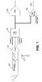
- FIG. 1shows a block diagram of laser power control circuitry in accordance with aspects of the invention.
- a photodetector 111receives light from a laser (not shown). The light may be derived, for example, from a back facet of the laser, with the photodiode approximate the back facet. Alternatively, light may be taken from a tap off a fiber optic line receiving light from the laser, in which case a wavelength locker may be used.
- the photodetectoror similar device, generates a current.
- the currentis provided on an input line to a semiconductor circuit.
- the input lineis coupled to a first input of a comparator 113 .
- the input lineis also coupled to ground by a resistance, providing a voltage on the input line.
- the resistanceis an adjustable resistance 117 .
- the adjustable resistanceis adjustable so as to allow a particular input voltage range to be set for the comparator, allowing for system optimization and particularly to account for a range of variations in photodetector output.
- Comparator 113receives a voltage set level 115 as a second input.
- the voltage set levelindicates a desired voltage level, selected to achieve a desired laser output power.
- the voltage set levelis a voltage equivalent to the expected voltage of the first input when the laser is transmitting data and properly biased.
- An output of the comparator 113accordingly indicates whether the laser output is above or below a desired level.
- the output of the comparator 113is provided to digital processing circuitry 121 .
- the digital processing circuitryconverts the output of the comparator 113 to a digital signal, averages the digital signal, and generates a multi-bit digital bias signal.
- the digital bias signalindicates a desired bias current for driving the laser.
- the digital bias signalis generated using an up-down counter, which counts up when the comparator output is high and counts down when the comparator is low.
- the laseroperates in a burst mode, with the laser periodically, or from time to time, changing from an operational mode (transmitting data) to a non-operational mode (not transmitting data). Delays may occur when the laser transitions from a non-operational mode to an operational mode while circuitry, such as comparator 113 , sufficiently charges for operation.
- a precharge block 119precharges the inputs to the comparator 113 .
- the precharge blockreceives a precharge signal.
- the precharge signalindicates a desired precharge level. More generally, the precharge signal merely indicates that precharging should occur.
- the precharge signalis generally set to indicate precharge when the laser is in the non-operational mode, and set to indicate no precharge during operation of the laser so as not to impact operation of the comparator 113 .
- the precharge signalcauses the precharge block to couple together the input lines to the comparator, effectively setting both inputs approximate to the voltage set level. In other embodiment, the precharge block sets either or both inputs to a desired precharge voltage.
- the digital processing circuitryis also provided a preload signal.
- the preload signalallows the digital processing circuitry to set, or preload, the digital bias signal to an initial bias value.
- the preload signaltherefore allows the digital bias signal to be set to an expected or desired value. This is beneficial as it may take some time for a counter, for example, to achieve a proper value, particularly when the laser operates in burst mode.
- the preload signalwhich may be externally provided, allows for direct control of the digital bias signal.
- the digital bias signalis provided to a digital-to-analog converter (DAC) 123 .
- the DACconverts the digital bias signal to an analog signal for conversion, for example, to a bias current signal for use in driving the laser.
- the digital bias signalis provided as a first input to a digital comparator 125 .
- the digital comparatorreceives as a second input a maximum bias signal.
- the maximum bias signalindicates a maximum allowable value for the bias signal.
- the bias signalreaches the maximum bias signal level when the laser is nearing the end of its useful life. Accordingly, the output of digital comparator 125 is an-end-of life (EOL) signal.
- FIG. 2illustrates a semi-schematic semi-block diagram of a further embodiment in accordance with the invention.
- a photodiode 211receives light from a laser (not shown).
- the photodiodegenerates a current based on the amount of light received.
- the currentflows from a cathode of the photodiode to an input pin 213 of a semiconductor circuit.
- the currentmay be termed a monitor diode current, and the pin may be termed a monitor diode pin.
- the pinis connected to an input line 215 .
- the input linecouples the input pin 219 to a first input of a comparator 217 by way of a resistor.
- the input lineis also coupled to ground by a plurality of selectable resistors 221 .
- the resistorsare selectable using a selection signal 223 .
- a plurality of selectable resistorsare provided, each individually controllable.
- the selectable resistorsare provided on chip, and may include, for example, twelve selectable resistors. In some embodiments a single resistor is selected for use at any given time, and each resistor has a different resistance.
- a bank of selectable capacitors 222is also provided.
- the capacitorsare selectable using a selection signal 224 .
- the selectable capacitorsare also provided on chip, and, for example, may include four capacitors. The capacitors allow for filtering of the monitor diode current, allowing a user to optimize monitor diode signal quality and response time.
- a comparator 217compares the voltage on the first input line to a voltage on a second input line.
- the voltage on the second input lineis a set voltage provided by a DAC 225 .
- the DACis provided a multi-bit data word indicating a desired set voltage, and generates the set voltage based on the multi-bit data word.
- the comparator inputsmay be precharged by use of a precharge signal. This is particularly useful when the transmitter is turned off and the photodiode is not receiving an input signal.
- a precharge signalis provided to a switch 227 .
- the switchcouples the output of the DAC 225 to the first input line. As illustrated, the connection to the first input line is between the input pin and the resistor between the input pin and the comparator. Closing the switch allows the comparator, as well as any capacitors or other storage devices, to remain charged and thereby reduce charging time when the transmitter transitions from off to on, particularly when a burst-on time is less than burst-off time.
- the output of the comparatoris provided to a clocked register 229 .
- the clocked registerstores a logical one when the set voltage is higher than the monitor diode voltage, stores a zero when the set voltage is lower than the monitor diode voltage, and provides the stored value as a digital signal.
- the digital signalis provided to a digital averager 231 .
- the digital averageraverages the digital signal data value to suppress transients, such as may occur due to data dependency.
- the digital averagerprovides an up-down signal to an up-down counter 233 .
- the up-down signalindicates that the up-down counter should either count up or count down.
- the digital averagerprovides a three valued signal, namely up-hold-down, or provides both an up-down signal and an up-down valid signal.
- the up-down counteralso receives a preload value signal and a load signal.
- the preload value signalprovides a value to which the output of the up-down counter should be set when the load signal is asserted.
- the load signalis asserted at power up.
- the load signalis asserted whenever the precharge signal is asserted.
- the load signalis asserted constantly so as to provide user control of the output of the counter throughout operation of the device.
- the output of the up-down counteris a multi-bit digital word indicating a desired bias level.
- the digital wordis provided to a DAC, which converts the digital word to a voltage.
- the voltage output by the DACis provided to voltage-to-current conversion and current mirrors block 237 .
- the voltage-to-current conversion and mirrors blockgenerate a bias current signal for use by the laser in some embodiments and for use by off-chip circuitry for driving the laser in other embodiments.
- the digital word from the up-down counteris also provided to a digital comparator 239 .
- the digital comparatorcompares the digital word with a digital word indicating a maximum bias signal.
- the output of the digital comparatorindicates when the up-down counter is attempting to set the digital word to a value outside the operating parameters for the bias signal.
- a burst enable signalindicates whether the laser is to transmit data.
- the clocked register, the counter and other clocked circuitsuse a transition in the burst enable signal, such as the transition from a non-transmit state to a transmit state, as a clock signal.
- the clock signalis selectable between a burst enable signal, or signal based thereon or indicative thereof, and another clock signal such as derived from a local oscillator.
- FIG. 3illustrates a further semi-block diagram semi-schematic of an automatic power control circuit in accordance with aspects of the invention.
- FIG. 3illustrates portions of a single chip semiconductor circuit 311 .
- the semiconductor circuitincludes a monitor diode input pin 313 .
- the monitor diode pinis coupled by way of a resistor 315 to a first input of a comparator 317 .
- the monitor diode pinis also coupled to ground by a bank of selectable resistors 319 , while the first input of a comparator is also coupled to ground by way of a bank of selectable capacitors 321 .
- the selectable resistorsare selected by way of a resistor selection signal.
- the resistance selection signalis stored on an on-chip register 323 a .
- the registeralong with registers 323 b - e , may be set by use of a programming interface or other similar interface. Similarly, capacitors of the selectable capacitor bank are selected by a capacitance selection signal, which is also set and stored in the on-chip registers.
- the comparatorcompares the first input, representative of the monitor diode signal, with the second input provided by a DAC 325 .
- the DAC 325sets the magnitude of the second input by converting a multi-bit digital input to an analog signal.
- the multi-bit digital inputis stored in register 323 b , which as indicated above may be set by the use of a programming interface or other similar interface. Accordingly, the register 323 b may be set by a user or preconfigured for operation to a value indicative of a particular voltage.
- the output of the DAC 325is coupled to the monitor diode input by a switch 327 .
- a logic block 329controls operation of the switch. The logic block receives a precharge disable signal 331 and burst enable signal 333 . The burst enable signal indicates burst mode is enabled. The logic block 329 sets the switch 327 to open when either the precharge disable signal indicates that precharge should be disabled or the burst enable signal indicates burst mode is enabled.
- the output of the comparator 317is provided to a digitizer 335 .
- the digitizerdigitizes the output of the comparator in a clocked manner, with the digitizer also receiving as a clock input the burst enable signal.
- the digitizeris a clocked register or a latch.
- the output of the digitizeris received by a digital averager 337 .
- the digital averageraverages the digitized data, for example to remove transient or data dependency effects.
- the output of the digital averageris provided as an up-down signal counter 339 .
- the countercounts up or down depending on the value received from the digital averager.
- the countercounts up and down in a clocked manner, with the counter receiving the burst enable signal as a clock signal.
- the counteralso receives a hold signal indicating the counter should not count up or down.
- the counteralso is able to be preloaded with a desired value.
- the desired valueis provided as a preload signal 341 .
- the preload signalis a multi-bit signal indicating a desired output value of the counter.
- the countersets its output to the value of the preload signal when a load signal is asserted.
- the load signalis asserted based on determination by logic block 343 . In many embodiments the load signal is asserted based on a user programmable command.
- a multi-bit output signal of the counteris provided to DAC 345 .
- the DAC 345converts the multi-bit signal to an analog voltage.
- the voltageis provided to a voltage-to-current converter 347 .
- the voltage-to-current converteris in a voltage-to-current converter block, and includes circuitry such as current mirrors for performing functions such as isolation of the output from the input and appropriate scaling of the output current.
- the output currentis a bias current.
- the bias currentis provided to bias circuitry 349 .
- a bias monitor voltageis also provided, in the embodiment of FIG. 3 by the voltage to current converter, to an analog MUX 351 .
- the analog MUXoutputs the bias monitor voltage, and other signals (not discussed) in accordance with a selection signal.
- the multi-bit output signal generated by the counter 339is also provided to a digital comparator 353 .
- the digital comparator 353also receives a multi-bit signal 355 .
- the multi-bit signal 355is stored in a register 323 e , and represents a maximum bias value. Generally the maximum bias value is a value approximate a maximum bias voltage, and often indicates that the laser is nearing the end of its useful life.
- the output of the digital comparatoris provided to a fault logic block 357 , which also receives a hold request signal and a disable EOL signal.
- the fault logic blockoutputs an end-of-life (EOL) signal and the hold signal, which was previously mentioned with respect to the counter block.
- EOLend-of-life
- the EOL signalis set when the digital comparator indicates the bias value has reached the maximum bias value and the disable EOL signal is not set.
- the hold signalis set when the bias value has reached the maximum bias value or the hold request signal is set.
- the hold request signalis user programmable, allowing a user, in conjunction with the preload signal, to set a specific bias value.
- FIG. 4illustrates signals in accordance with aspects of the invention, such as associated with FIG. 1 , 2 or 3 .
- Input data 411shows data received at a monitor diode pin.
- the input datareflects activation of a laser during time periods, such as time periods 413 and 415 .
- time period 417which is between time period 413 and 415 .
- the laseris inactive.
- the laseris active during burst enable periods, as shown by a burst enable signal 419 .
- the burst enable signalalso makes from a high level to a low level, with transmission by the laser enabled during burst enable.
- a desired bias current 421is indicated in conjunction with output bias current 423 . At time to the output bias current is below the desired bias current.
- FIG. 4also shows the bias DAC counter output 425 .
- the bias DAC counter outputis initially at a hex value which is three values below the desired bias current.
- the desired bias currentis XXXh
- the bias DAC counter outputat time to being XXXh-3LSBh and at time to the counter output is equal to the value provided by the bias preload signal.
- a time t 3 operation of the circuitsuch as circuits of FIG. 1 , 2 or 3 , with clocked circuitry of those figures clocked on a rising edge of a burst enable signal, achieves a bias DAC counter output of XXXh and a corresponding output bias current equal to a desired bias current.
- the desired bias current outputthereafter toggles, in response to changes to the bias DAC counter output of one least significant bit as the counter toggles.
- the inventionprovides that some aspects an automatic power control circuit for a laser driver.
Landscapes
- Physics & Mathematics (AREA)
- Condensed Matter Physics & Semiconductors (AREA)
- General Physics & Mathematics (AREA)
- Electromagnetism (AREA)
- Optics & Photonics (AREA)
- Semiconductor Lasers (AREA)
Abstract
Description
Claims (21)
Priority Applications (1)
| Application Number | Priority Date | Filing Date | Title |
|---|---|---|---|
| US11/221,609US7516897B1 (en) | 2005-09-07 | 2005-09-07 | Digital automatic power control loop for continuous and burst mode applications |
Applications Claiming Priority (1)
| Application Number | Priority Date | Filing Date | Title |
|---|---|---|---|
| US11/221,609US7516897B1 (en) | 2005-09-07 | 2005-09-07 | Digital automatic power control loop for continuous and burst mode applications |
Publications (1)
| Publication Number | Publication Date |
|---|---|
| US7516897B1true US7516897B1 (en) | 2009-04-14 |
Family
ID=40525038
Family Applications (1)
| Application Number | Title | Priority Date | Filing Date |
|---|---|---|---|
| US11/221,609Expired - Fee RelatedUS7516897B1 (en) | 2005-09-07 | 2005-09-07 | Digital automatic power control loop for continuous and burst mode applications |
Country Status (1)
| Country | Link |
|---|---|
| US (1) | US7516897B1 (en) |
Cited By (1)
| Publication number | Priority date | Publication date | Assignee | Title |
|---|---|---|---|---|
| US10256913B2 (en)* | 2017-06-29 | 2019-04-09 | Renesas Electronics Corporation | Optical driving device and optical communication system |
Citations (17)
| Publication number | Priority date | Publication date | Assignee | Title |
|---|---|---|---|---|
| US5216659A (en)* | 1991-09-11 | 1993-06-01 | International Business Machines | Laser power calibration by measuring laser drive current at out of focus and in focus conditions |
| US5696370A (en)* | 1995-02-28 | 1997-12-09 | Psc Inc. | Bar code scanning system for automatically calculating the optical power output levels of the light source |
| US5999549A (en) | 1998-02-09 | 1999-12-07 | International Business Machines Corporation | Method and apparatus for laser safety |
| US20020054409A1 (en)* | 2000-09-05 | 2002-05-09 | Meir Bartur | Fiber optic transceiver employing clock and data phase aligner |
| US20020149821A1 (en) | 2001-02-05 | 2002-10-17 | Aronson Lewis B. | Integrated memory mapped controller circuit for fiber optics transceiver |
| US6697400B2 (en) | 2001-02-08 | 2004-02-24 | Nec Corporation | Circuit for driving a laser diode which has a feed-forward type APC circuit and method for driving a laser diode by using the APC circuit |
| US6697397B2 (en)* | 2001-11-15 | 2004-02-24 | Alcatel | Wavelength compensated ALC loop |
| US6707833B1 (en) | 2000-03-31 | 2004-03-16 | Marconi Communications, Inc. | Digital laser driver circuit |
| US6792020B2 (en) | 2002-08-05 | 2004-09-14 | Agilent Technologies, Inc. | Laser driver with a safety circuit having digital feedback |
| US6810051B2 (en) | 2002-01-22 | 2004-10-26 | Telefonaktiebolaget Lm Ericsson (Publ) | Apparatus and method for laser driver operation |
| US6834065B2 (en) | 2002-05-21 | 2004-12-21 | Carrier Access Corporation | Methods and apparatuses for direct digital drive of a laser in a passive optical network |
| US6885685B2 (en) | 2002-06-11 | 2005-04-26 | Sumitomo Electric Industries, Ltd. | Control system for a laser diode and a method for controlling the same |
| US6885684B2 (en) | 2002-04-25 | 2005-04-26 | Sumitomo Electric Industries, Ltd. | Laser control circuit and laser module |
| US20050129075A1 (en)* | 2003-12-15 | 2005-06-16 | Anderson Douglas P. | Laser turn-on accelerator independent of bias control loop bandwidth |
| US20060215716A1 (en)* | 2005-03-25 | 2006-09-28 | Pavilion Integration Corporation | Radio frequency modulation of variable degree and automatic power control using external photodiode sensor for low-noise lasers of various wavelengths |
| US7215891B1 (en)* | 2003-06-06 | 2007-05-08 | Jds Uniphase Corporation | Integrated driving, receiving, controlling, and monitoring for optical transceivers |
| US7317874B2 (en)* | 2006-06-02 | 2008-01-08 | Broadway Networks, Inc. | Adaptive optical transceiver for fiber access communications |
- 2005
- 2005-09-07USUS11/221,609patent/US7516897B1/ennot_activeExpired - Fee Related
Patent Citations (19)
| Publication number | Priority date | Publication date | Assignee | Title |
|---|---|---|---|---|
| US5216659A (en)* | 1991-09-11 | 1993-06-01 | International Business Machines | Laser power calibration by measuring laser drive current at out of focus and in focus conditions |
| US5696370A (en)* | 1995-02-28 | 1997-12-09 | Psc Inc. | Bar code scanning system for automatically calculating the optical power output levels of the light source |
| US5834750A (en)* | 1995-02-28 | 1998-11-10 | Psc, Inc. | Bar code scanning system for automatically maintaining constant the amplitude of light reflected from a bar code |
| US5999549A (en) | 1998-02-09 | 1999-12-07 | International Business Machines Corporation | Method and apparatus for laser safety |
| US6707833B1 (en) | 2000-03-31 | 2004-03-16 | Marconi Communications, Inc. | Digital laser driver circuit |
| US20020054409A1 (en)* | 2000-09-05 | 2002-05-09 | Meir Bartur | Fiber optic transceiver employing clock and data phase aligner |
| US20020149821A1 (en) | 2001-02-05 | 2002-10-17 | Aronson Lewis B. | Integrated memory mapped controller circuit for fiber optics transceiver |
| US6697400B2 (en) | 2001-02-08 | 2004-02-24 | Nec Corporation | Circuit for driving a laser diode which has a feed-forward type APC circuit and method for driving a laser diode by using the APC circuit |
| US6697397B2 (en)* | 2001-11-15 | 2004-02-24 | Alcatel | Wavelength compensated ALC loop |
| US6810051B2 (en) | 2002-01-22 | 2004-10-26 | Telefonaktiebolaget Lm Ericsson (Publ) | Apparatus and method for laser driver operation |
| US6885684B2 (en) | 2002-04-25 | 2005-04-26 | Sumitomo Electric Industries, Ltd. | Laser control circuit and laser module |
| US6834065B2 (en) | 2002-05-21 | 2004-12-21 | Carrier Access Corporation | Methods and apparatuses for direct digital drive of a laser in a passive optical network |
| US6885685B2 (en) | 2002-06-11 | 2005-04-26 | Sumitomo Electric Industries, Ltd. | Control system for a laser diode and a method for controlling the same |
| US6792020B2 (en) | 2002-08-05 | 2004-09-14 | Agilent Technologies, Inc. | Laser driver with a safety circuit having digital feedback |
| US7215891B1 (en)* | 2003-06-06 | 2007-05-08 | Jds Uniphase Corporation | Integrated driving, receiving, controlling, and monitoring for optical transceivers |
| US20050129075A1 (en)* | 2003-12-15 | 2005-06-16 | Anderson Douglas P. | Laser turn-on accelerator independent of bias control loop bandwidth |
| US7203213B2 (en)* | 2003-12-15 | 2007-04-10 | Micrel, Incorporated | Laser turn-on accelerator independent of bias control loop bandwidth |
| US20060215716A1 (en)* | 2005-03-25 | 2006-09-28 | Pavilion Integration Corporation | Radio frequency modulation of variable degree and automatic power control using external photodiode sensor for low-noise lasers of various wavelengths |
| US7317874B2 (en)* | 2006-06-02 | 2008-01-08 | Broadway Networks, Inc. | Adaptive optical transceiver for fiber access communications |
Non-Patent Citations (1)
| Title |
|---|
| Wirbel, Loring, "Driver For Passive Optical Nets Touts Integration", EE Times, May 16, 2005 (3 pgs.). |
Cited By (1)
| Publication number | Priority date | Publication date | Assignee | Title |
|---|---|---|---|---|
| US10256913B2 (en)* | 2017-06-29 | 2019-04-09 | Renesas Electronics Corporation | Optical driving device and optical communication system |
Similar Documents
| Publication | Publication Date | Title |
|---|---|---|
| US6282216B1 (en) | Burst mode optical transmitter circuit | |
| US10651933B1 (en) | Thermal calibration of a ring modulator | |
| US7085943B2 (en) | Method and circuitry for controlling supply voltage in a data processing system | |
| EP0034957B1 (en) | Automatic output power regulating device for the emitter module of a fibre-optical transmission system | |
| EP1282207A1 (en) | Light transmitter | |
| US6792020B2 (en) | Laser driver with a safety circuit having digital feedback | |
| US7443896B2 (en) | Optical midpoint power control and extinction ratio control of a semiconductor laser | |
| US7480320B2 (en) | Semiconductor laser driving device, semiconductor laser driving method, and image forming apparatus using semiconductor laser driving device | |
| US6597485B1 (en) | Optical transmitter circuit | |
| US6329843B1 (en) | Output driver with current compensation circuit for variation of common mode voltage | |
| US6292284B1 (en) | Light emitting element driving apparatus | |
| US6862379B2 (en) | Extinction ratio control of a semiconductor laser | |
| JP2011528209A (en) | Method and system for closed-loop control of an optical link | |
| JPH11239105A (en) | Optical transmitter and optical transmission system using the same | |
| US8103174B2 (en) | Transmission network having an optical receiver that utilizes dual power pins and a single status pin to lower power consumption, lower manufacturing cost, and increase transmission efficiency | |
| US7411986B2 (en) | Optical system laser driver with a built in output inductor for improved frequency response | |
| EP1989802B1 (en) | Transmission network having an optical receiver that utilizes dual power pins and a single status pin to lower power consumption, lower manufacturing cost, and increase transmission efficiency | |
| US7516897B1 (en) | Digital automatic power control loop for continuous and burst mode applications | |
| US6466041B1 (en) | Method for setting the trigger power of transmitter diodes | |
| JP2001358661A (en) | Optical transmission circuit | |
| US10749605B2 (en) | Laser power controller | |
| US6728495B1 (en) | Light output control circuit with a warning function of deteriorated light output | |
| KR101772593B1 (en) | Analog-digital converter with self-reflecting the change in temperature environment | |
| JP2006311130A (en) | Optical receiver | |
| JP4213945B2 (en) | Semiconductor laser drive device |
Legal Events
| Date | Code | Title | Description |
|---|---|---|---|
| AS | Assignment | Owner name:OBSIDIAN, LLC, AS COLLATERAL AGENT, CALIFORNIA Free format text:SECURITY AGREEMENT;ASSIGNOR:VITESSE SEMICONDUCTOR CORPORATION;REEL/FRAME:017846/0847 Effective date:20060607 Owner name:OBSIDIAN, LLC, AS COLLATERAL AGENT,CALIFORNIA Free format text:SECURITY AGREEMENT;ASSIGNOR:VITESSE SEMICONDUCTOR CORPORATION;REEL/FRAME:017846/0847 Effective date:20060607 | |
| AS | Assignment | Owner name:VITESSE SEMICONDUCTOR CORPORATION, CALIFORNIA Free format text:RELEASE BY SECURED PARTY;ASSIGNOR:OBSIDIAN, LLC;REEL/FRAME:023373/0053 Effective date:20091014 Owner name:VITESSE SEMICONDUCTOR CORPORATION,CALIFORNIA Free format text:RELEASE BY SECURED PARTY;ASSIGNOR:OBSIDIAN, LLC;REEL/FRAME:023373/0053 Effective date:20091014 | |
| AS | Assignment | Owner name:VITESSE SEMICONDUCTOR CORPORATION, CALIFORNIA Free format text:RELEASE BY SECURED PARTY;ASSIGNOR:OBSIDIAN, LLC;REEL/FRAME:023438/0587 Effective date:20091014 Owner name:VLTESSE INTERNATIONAL, INC., CALIFORNIA Free format text:RELEASE BY SECURED PARTY;ASSIGNOR:OBSIDIAN, LLC;REEL/FRAME:023438/0587 Effective date:20091014 Owner name:VITESSE MANUFACTURING & DEVELOPMENT CORPORATION, C Free format text:RELEASE BY SECURED PARTY;ASSIGNOR:OBSIDIAN, LLC;REEL/FRAME:023438/0587 Effective date:20091014 Owner name:VITESSE SEMICONDUCTOR SALES CORPORATION, CALIFORNI Free format text:RELEASE BY SECURED PARTY;ASSIGNOR:OBSIDIAN, LLC;REEL/FRAME:023438/0587 Effective date:20091014 Owner name:VITESSE SEMICONDUCTOR CORPORATION,CALIFORNIA Free format text:RELEASE BY SECURED PARTY;ASSIGNOR:OBSIDIAN, LLC;REEL/FRAME:023438/0587 Effective date:20091014 Owner name:VLTESSE INTERNATIONAL, INC.,CALIFORNIA Free format text:RELEASE BY SECURED PARTY;ASSIGNOR:OBSIDIAN, LLC;REEL/FRAME:023438/0587 Effective date:20091014 Owner name:VITESSE MANUFACTURING & DEVELOPMENT CORPORATION,CA Free format text:RELEASE BY SECURED PARTY;ASSIGNOR:OBSIDIAN, LLC;REEL/FRAME:023438/0587 Effective date:20091014 Owner name:VITESSE SEMICONDUCTOR SALES CORPORATION,CALIFORNIA Free format text:RELEASE BY SECURED PARTY;ASSIGNOR:OBSIDIAN, LLC;REEL/FRAME:023438/0587 Effective date:20091014 | |
| AS | Assignment | Owner name:U.S. BANK NATIONAL ASSOCIATION, MINNESOTA Free format text:COLLATERAL ASSIGNMENT (INTELLECTUAL PROPERTY);ASSIGNOR:VITESSE SEMICONDUCTOR CORPORATION;REEL/FRAME:023471/0267 Effective date:20091030 Owner name:U.S. BANK NATIONAL ASSOCIATION,MINNESOTA Free format text:COLLATERAL ASSIGNMENT (INTELLECTUAL PROPERTY);ASSIGNOR:VITESSE SEMICONDUCTOR CORPORATION;REEL/FRAME:023471/0267 Effective date:20091030 | |
| AS | Assignment | Owner name:WHITEBOX VSC, LTD., MINNESOTA Free format text:SECURITY AGREEMENT;ASSIGNOR:VITESSE SEMICONDUCTOR CORPORATION;REEL/FRAME:023627/0079 Effective date:20071029 Owner name:WHITEBOX VSC, LTD.,MINNESOTA Free format text:SECURITY AGREEMENT;ASSIGNOR:VITESSE SEMICONDUCTOR CORPORATION;REEL/FRAME:023627/0079 Effective date:20071029 | |
| CC | Certificate of correction | ||
| AS | Assignment | Owner name:VITESSE SEMICONDUCTOR CORPORATION,CALIFORNIA Free format text:ASSIGNMENT OF ASSIGNORS INTEREST;ASSIGNORS:HUSSAIN, KINANA;WU, ADAM;CHOI, LAWRENCE;SIGNING DATES FROM 20100308 TO 20100310;REEL/FRAME:024611/0836 Owner name:VITESSE SEMICONDUCTOR CORPORATION,CALIFORNIA Free format text:ASSIGNMENT OF ASSIGNORS INTEREST;ASSIGNOR:MAYAMPURATH, BALAGOPAL;REEL/FRAME:024611/0845 Effective date:20100626 | |
| FPAY | Fee payment | Year of fee payment:4 | |
| AS | Assignment | Owner name:VITESSE SEMICONDUCTOR CORPORATION, CALIFORNIA Free format text:RELEASE BY SECURED PARTY;ASSIGNOR:US BANK NATIONAL ASSOCIATION, AS COLLATERAL AGENT;REEL/FRAME:034176/0162 Effective date:20141103 | |
| AS | Assignment | Owner name:VITESSE SEMICONDUCTOR CORPORATION, CALIFORNIA Free format text:RELEASE BY SECURED PARTY;ASSIGNOR:WHITEBOX VSC, LTD.;REEL/FRAME:035526/0090 Effective date:20150428 | |
| AS | Assignment | Owner name:BANK OF AMERICA, N.A., AS COLLATERAL AGENT, NORTH Free format text:SUPPLEMENTAL SECURITY AGREEMENT;ASSIGNOR:MICROSEMI COMMUNICATIONS, INC.;REEL/FRAME:035532/0925 Effective date:20150428 | |
| AS | Assignment | Owner name:MICROSEMI COMMUNICATIONS, INC., CALIFORNIA Free format text:MERGER AND CHANGE OF NAME;ASSIGNORS:VITESSE SEMICONDUCTOR CORPORATION;LLIU100 ACQUISITION CORP.;REEL/FRAME:035651/0708 Effective date:20150428 | |
| AS | Assignment | Owner name:MICROSEMI SOC CORP., A CALIFORNIA CORPORATION, CAL Free format text:RELEASE BY SECURED PARTY;ASSIGNOR:BANK OF AMERICA, N.A.;REEL/FRAME:037558/0711 Effective date:20160115 Owner name:MICROSEMI FREQUENCY AND TIME CORPORATION, A DELAWA Free format text:RELEASE BY SECURED PARTY;ASSIGNOR:BANK OF AMERICA, N.A.;REEL/FRAME:037558/0711 Effective date:20160115 Owner name:MICROSEMI CORP.-MEMORY AND STORAGE SOLUTIONS (F/K/ Free format text:RELEASE BY SECURED PARTY;ASSIGNOR:BANK OF AMERICA, N.A.;REEL/FRAME:037558/0711 Effective date:20160115 Owner name:MICROSEMI CORPORATION, CALIFORNIA Free format text:RELEASE BY SECURED PARTY;ASSIGNOR:BANK OF AMERICA, N.A.;REEL/FRAME:037558/0711 Effective date:20160115 Owner name:MICROSEMI COMMUNICATIONS, INC. (F/K/A VITESSE SEMI Free format text:RELEASE BY SECURED PARTY;ASSIGNOR:BANK OF AMERICA, N.A.;REEL/FRAME:037558/0711 Effective date:20160115 Owner name:MICROSEMI SEMICONDUCTOR (U.S.) INC., A DELAWARE CO Free format text:RELEASE BY SECURED PARTY;ASSIGNOR:BANK OF AMERICA, N.A.;REEL/FRAME:037558/0711 Effective date:20160115 Owner name:MICROSEMI CORP.-ANALOG MIXED SIGNAL GROUP, A DELAW Free format text:RELEASE BY SECURED PARTY;ASSIGNOR:BANK OF AMERICA, N.A.;REEL/FRAME:037558/0711 Effective date:20160115 | |
| AS | Assignment | Owner name:MORGAN STANLEY SENIOR FUNDING, INC., NEW YORK Free format text:PATENT SECURITY AGREEMENT;ASSIGNORS:MICROSEMI CORPORATION;MICROSEMI SEMICONDUCTOR (U.S.) INC. (F/K/A LEGERITY, INC., ZARLINK SEMICONDUCTOR (V.N.) INC., CENTELLAX, INC., AND ZARLINK SEMICONDUCTOR (U.S.) INC.);MICROSEMI FREQUENCY AND TIME CORPORATION (F/K/A SYMMETRICON, INC.);AND OTHERS;REEL/FRAME:037691/0697 Effective date:20160115 | |
| REMI | Maintenance fee reminder mailed | ||
| LAPS | Lapse for failure to pay maintenance fees | ||
| STCH | Information on status: patent discontinuation | Free format text:PATENT EXPIRED DUE TO NONPAYMENT OF MAINTENANCE FEES UNDER 37 CFR 1.362 | |
| FP | Lapsed due to failure to pay maintenance fee | Effective date:20170414 | |
| AS | Assignment | Owner name:MICROSEMI CORP. - RF INTEGRATED SOLUTIONS, CALIFOR Free format text:RELEASE BY SECURED PARTY;ASSIGNOR:MORGAN STANLEY SENIOR FUNDING, INC.;REEL/FRAME:046251/0391 Effective date:20180529 Owner name:MICROSEMI SEMICONDUCTOR (U.S.), INC., CALIFORNIA Free format text:RELEASE BY SECURED PARTY;ASSIGNOR:MORGAN STANLEY SENIOR FUNDING, INC.;REEL/FRAME:046251/0391 Effective date:20180529 Owner name:MICROSEMI CORPORATION, CALIFORNIA Free format text:RELEASE BY SECURED PARTY;ASSIGNOR:MORGAN STANLEY SENIOR FUNDING, INC.;REEL/FRAME:046251/0391 Effective date:20180529 Owner name:MICROSEMI FREQUENCY AND TIME CORPORATION, CALIFORN Free format text:RELEASE BY SECURED PARTY;ASSIGNOR:MORGAN STANLEY SENIOR FUNDING, INC.;REEL/FRAME:046251/0391 Effective date:20180529 Owner name:MICROSEMI CORP. - POWER PRODUCTS GROUP, CALIFORNIA Free format text:RELEASE BY SECURED PARTY;ASSIGNOR:MORGAN STANLEY SENIOR FUNDING, INC.;REEL/FRAME:046251/0391 Effective date:20180529 Owner name:MICROSEMI COMMUNICATIONS, INC., CALIFORNIA Free format text:RELEASE BY SECURED PARTY;ASSIGNOR:MORGAN STANLEY SENIOR FUNDING, INC.;REEL/FRAME:046251/0391 Effective date:20180529 Owner name:MICROSEMI SOC CORP., CALIFORNIA Free format text:RELEASE BY SECURED PARTY;ASSIGNOR:MORGAN STANLEY SENIOR FUNDING, INC.;REEL/FRAME:046251/0391 Effective date:20180529 |