US7512847B2 - Method for estimating and reporting the life expectancy of flash-disk memory - Google Patents
Method for estimating and reporting the life expectancy of flash-disk memoryDownload PDFInfo
- Publication number
- US7512847B2 US7512847B2US11/702,500US70250007AUS7512847B2US 7512847 B2US7512847 B2US 7512847B2US 70250007 AUS70250007 AUS 70250007AUS 7512847 B2US7512847 B2US 7512847B2
- Authority
- US
- United States
- Prior art keywords
- memory device
- memory
- value
- grade
- data
- Prior art date
- Legal status (The legal status is an assumption and is not a legal conclusion. Google has not performed a legal analysis and makes no representation as to the accuracy of the status listed.)
- Active, expires
Links
Images


Classifications
- G—PHYSICS
- G06—COMPUTING OR CALCULATING; COUNTING
- G06F—ELECTRIC DIGITAL DATA PROCESSING
- G06F13/00—Interconnection of, or transfer of information or other signals between, memories, input/output devices or central processing units
- G—PHYSICS
- G11—INFORMATION STORAGE
- G11C—STATIC STORES
- G11C29/00—Checking stores for correct operation ; Subsequent repair; Testing stores during standby or offline operation
- G11C29/52—Protection of memory contents; Detection of errors in memory contents
- G—PHYSICS
- G06—COMPUTING OR CALCULATING; COUNTING
- G06F—ELECTRIC DIGITAL DATA PROCESSING
- G06F12/00—Accessing, addressing or allocating within memory systems or architectures
- G—PHYSICS
- G06—COMPUTING OR CALCULATING; COUNTING
- G06F—ELECTRIC DIGITAL DATA PROCESSING
- G06F9/00—Arrangements for program control, e.g. control units
- G06F9/06—Arrangements for program control, e.g. control units using stored programs, i.e. using an internal store of processing equipment to receive or retain programs
- G—PHYSICS
- G11—INFORMATION STORAGE
- G11C—STATIC STORES
- G11C16/00—Erasable programmable read-only memories
- G11C16/02—Erasable programmable read-only memories electrically programmable
- G11C16/06—Auxiliary circuits, e.g. for writing into memory
- G11C16/34—Determination of programming status, e.g. threshold voltage, overprogramming or underprogramming, retention
- G11C16/349—Arrangements for evaluating degradation, retention or wearout, e.g. by counting erase cycles
- G—PHYSICS
- G11—INFORMATION STORAGE
- G11C—STATIC STORES
- G11C29/00—Checking stores for correct operation ; Subsequent repair; Testing stores during standby or offline operation
- G11C29/04—Detection or location of defective memory elements, e.g. cell constructio details, timing of test signals
- G11C29/08—Functional testing, e.g. testing during refresh, power-on self testing [POST] or distributed testing
- G11C29/12—Built-in arrangements for testing, e.g. built-in self testing [BIST] or interconnection details
- G11C29/38—Response verification devices
- G11C29/42—Response verification devices using error correcting codes [ECC] or parity check
- G—PHYSICS
- G11—INFORMATION STORAGE
- G11C—STATIC STORES
- G11C29/00—Checking stores for correct operation ; Subsequent repair; Testing stores during standby or offline operation
- G11C29/04—Detection or location of defective memory elements, e.g. cell constructio details, timing of test signals
- G11C29/50—Marginal testing, e.g. race, voltage or current testing
- G—PHYSICS
- G11—INFORMATION STORAGE
- G11C—STATIC STORES
- G11C16/00—Erasable programmable read-only memories
- G11C16/02—Erasable programmable read-only memories electrically programmable
- G11C16/04—Erasable programmable read-only memories electrically programmable using variable threshold transistors, e.g. FAMOS
- G—PHYSICS
- G11—INFORMATION STORAGE
- G11C—STATIC STORES
- G11C29/00—Checking stores for correct operation ; Subsequent repair; Testing stores during standby or offline operation
- G11C29/04—Detection or location of defective memory elements, e.g. cell constructio details, timing of test signals
- G11C2029/0409—Online test
- G—PHYSICS
- G11—INFORMATION STORAGE
- G11C—STATIC STORES
- G11C29/00—Checking stores for correct operation ; Subsequent repair; Testing stores during standby or offline operation
- G11C29/04—Detection or location of defective memory elements, e.g. cell constructio details, timing of test signals
- G11C29/50—Marginal testing, e.g. race, voltage or current testing
- G11C2029/5002—Characteristic
Definitions
- the present inventionrelates to methods for built-in detection of the deterioration of reliability in digital memory devices in general, and in removable flash-memory devices in particular.
- Non-volatile storage systemsinclude a memory and a control system, which sometimes reside on the same piece of silicon. One of the tasks performed by the control system is error correction.
- ECCError-correction code detects occasional errors in the data, generated by the storage element's nature or the characteristics of the operating environment, fixes the error, and delivers the corrected original information upon a user's request.
- the ECC systemhas a built-in limitation with regard to the number of errors that can be corrected. Upon encountering an excessive number of errors, the information cannot be repaired, and may be reported as lost, or may be sent with the errors to the user.
- the current state of the artdoes not provide a way to report the “health” (i.e. operational-reliability performance) of a memory device. While some prior art methods record the usage of the device (i.e. the number of times the device is written to) for internal load-balancing purposes, the methods are not designed for the purpose of providing an early-warning indication to a user or application. While there is a correlation between the usage of the device and the device's remaining life expectancy, such a correlation is not absolute since there is a natural, random variability among devices (similar to the inaccuracy of predicting a person's life expectancy based on age only).
- the present inventionprovides methods for built-in detection of the deterioration of reliability in digital memory devices in general, and in removable flash-memory devices in particular.
- the present inventiondescribes flash-memory devices as a typical example, but is applicable to, and intended to cover, any memory device.
- the term “longevity parameter”is used in this application to refer to a variable of a memory device whose value changes during the life of the memory device, represents a relative deteriorated health of at least one cell of the memory device, and correlates with the device's life expectancy.
- Such parametersinclude, for example: the average number of errors, the number of programming cycles, and the number of bits that flipped logic state (upon the first programming pulse of a programming operation) when the bits are written to the memory.
- the present inventionapplies to both single-level-cell (SLC) flash memories and multi-level-cell (MLC) flash memories. While the subsequent discussion focuses primarily on SLC cells, it will be clear to those skilled in the art how the present invention applies to MLC cells.
- the terms “erasing” and “writing”are used herein to refer to setting threshold voltages of a memory cell, where erasing typically sets the voltages to correspond to one-logic states, and writing typically sets the voltages to correspond to zero-logic states for SLC cells.
- writingand “programming” are used interchangeably herein.
- the present inventionis particularly applicable to NAND-type flash memories that are read and programmed a page at a time.
- blockis used in this application to refer to the smallest number of cells, in a memory, that can be erased in a single operation.
- pageis used in this application to refer to the smallest number of cells, in a memory, that that can be written in a single operation. Typically, there are multiple pages in a block.
- gradeis used in this application to refer to a measure of the reliability of a memory page or block based on the values of the page's or block's longevity parameters. It is noted that an erase-operation is typically performed on a block (as opposed to a page). Thus, in the context of erase-operations, the grade refers to a measure of the reliability of a block based on the block's longevity parameters.
- initial healthis used in this application to refer to a longevity parameter that represents the deviation of the grade of a page or block from some reference value. Blocks can start their “lives” with different initial healths.
- relative deteriorated healthis used in this application to refer to the deterioration of the health of a block or page from an initial health since the block was produced and tested. The health of blocks can deteriorate at different rates.
- health cellsis used in this application to refer to cells that have successfully changed logic states after a sequence of programming pulses associated with a data operation.
- memory deviceis used in this application to refer to any non-volatile memory that stores data via a physical process that can result in errors.
- memory devicesinclude portable and stationary devices, based on semiconductor, magnetic, holographic, optical, and other physical binary-logic memory-technologies.
- FIG. 1is a flowchart of the operational procedure for a typical write-operation of a SLC NAND-type flash-memory device.
- a controller of the memory of a flash-memory deviceinstructs the memory to write certain information to a page
- the memoryconducts a series of operations.
- the datais first written to a memory buffer (Block 10 ).
- the destination of the write-operation datai.e. the physical location in the memory, or “word line”
- the programming stepis divided into several short programming pulses. The first pulse is applied to program all bits that are to be programmed (Block 14 ).
- the programmed bitsare checked to verify that the bits have met the threshold level (this level is higher than a standard read threshold-level) (Block 16 ). If not all of the bits are at the correct values (Block 18 ), an additional programming cycle is performed (Block 20 ). Optionally, the additional cycle may be performed with higher voltage (Block 20 ). When all of the bits match the buffer values, the program cycle (i.e. write-operation) is finished (Block 22 ).
- the programming cyclesutilize gradually increasing levels of voltage until the end of the write-operation.
- the difference between the first and second pulsesis much higher than the subsequent pulses. In such a case, an option to increase the voltage in small steps after a few initial large increments is utilized.
- the process of selectively writing (i.e. programming) data to a flash memoryinvolves changing logic states of selected memory cells, typically, in a SLC implementation, from one-logic to zero-logic.
- the process of selectively erasing data from a flash memoryinvolves changing values of selected memory cells, typically from zero-logic to one-logic.
- this designationis arbitrary, and would be equally implementable in the opposite designation.
- NAND-type flash memorieshave one or more page buffers (i.e. memory cells with read/write capability), which receive the data before the data is programmed into the flash memory cells.
- Page-programming methodsfor flash memory in which each flash memory cell contains one bit of information and erased flash memory cells have one-logic, implement the following steps:
- the present inventionincludes several preferred embodiments in which the memory controller of a flash-memory device can detect symptoms of deterioration in the flash-memory device, and provide a reliable prediction of the life expectancy of the flash-memory device.
- a longevity parameterderived from a grade, serves as a “forecast” of the life expectancy of the flash-memory device.
- a device having a poorer longevity parameteris indicative of a relatively shorter life expectancy than a device with a better longevity parameter.
- the systemmonitors the probability of error in reading data from the flash memory. Usually, this statistic is available to the ECC of the flash-memory controller, and does not require any direct access to the flash memory itself. In some flash-memory devices, the ECC is built into the flash memory itself. In such devices, information about the number of errors is made available to the memory controller by a command.
- the systemmonitors either the average or the maximum number of pulses required to change the state of a data bit during programming.
- this numbertypically ranges from 4 to 25 programming pulses (depending on the type of flash memory). As the flash memory deteriorates, the number of pulses required to write the data to the flash memory increases.
- the systemmonitors the number of successful changes of logic state of data bits after a given number of pulses. For example, the numbers of bits that are correctly programmed after the first pulse decreases with the deterioration of the flash memory as more bits require more than one pulse for writing.
- a method for managing a memory deviceincluding: (a) monitoring a value of a longevity parameter of the memory device after a data operation on the memory device, the monitoring being performed by the memory device; and (b) deriving a grade of the memory device from the value.
- the longevity parameteris a ratio of successfully-processed data to unsuccessfully-processed data.
- the longevity parameteris a deviation in a power consumption of the memory device.
- the deviationis an average of measurements for a plurality of the operations.
- the gradeserves as a forecast of a life expectancy of the memory.
- the operationis a programming operation
- the valueis a number of programming pulses, associated with the operation, required to change logic states of at least one cell in a page of the memory device.
- the operationis an erase operation
- the valueis a number of programming pulses, associated with the operation, required to change logic states of at least one cell in a block of the memory device.
- the operationis a programming operation
- the valueis a number of healthy cells in a page of the memory device.
- the operationis an erase operation
- the valueis a number of healthy cells in a block of the memory device.
- the operationis selected from the group consisting of: writing data, reading data, and erasing data.
- the gradeis selected from the group consisting of: a comparison grade of a current value to a pre-determined reference value, a maximum grade of a plurality of the values stored in a monitoring device, and an average grade of the plurality of the values stored in the monitoring device.
- the methodfurther includes the step of: (c) storing the pre-determined reference value in the memory device upon manufacture of the memory device.
- the step of monitoringincludes accessing the memory device for the purpose of deriving the grade.
- the methodfurther includes the step of: (c) storing the grade in a monitoring device.
- the monitoring deviceis selected from the group consisting of: the memory device, an embedded controller of the memory device, and a host system of the memory device.
- the step of derivingis initiated by the memory device.
- the step of derivingis initiated by a host system of the memory device.
- the step of derivingis initiated by an embedded controller of the memory device.
- the step of derivingis initiated by an application running on a host system.
- the step of derivingis initiated by an operating system running on a host system.
- a memory device for managing dataincluding: (a) a memory; and (b) a controller operative: (i) to monitor a value of a longevity parameter after a data operation on the memory; and (ii) to derive a grade of the memory device from the value.
- the gradeserves as a forecast of a life expectancy of the memory device.
- a system for managing dataincluding: (a) a memory device including a memory; and (b) a processor, housed in said memory device, operative: (i) to monitor a value of a longevity parameter after a data operation on the memory; and (ii) to derive a grade of the memory device from the value.
- the gradeserves as a forecast of a life expectancy of the memory device.
- FIG. 1is a flowchart of the operational procedure for a typical write-operation of a flash-memory device
- FIG. 2shows a qualitative graph of the degradation of the grade of a data page (or block) of a memory device as a function of time, according to a preferred embodiment of the present invention
- FIG. 3Ais a flowchart of the operational procedure for a method for monitoring the number of errors that are discovered and fixed by a memory controller, according to a preferred embodiment of the present invention
- FIG. 3Bis a flowchart of the operational procedure for a method for reporting the health of a memory device to a host system, according to a preferred embodiment of the present invention
- FIG. 4Ais a simplified schematic diagram of the format of a typical data page, according to both the prior art and the present invention.
- FIG. 4Bis a simplified schematic diagram of the format of a data page that includes a grade of the page, according to a preferred embodiment of the present invention.
- FIG. 5is a flowchart of the operational procedure for a method for monitoring the number of pulses required for writing a page, and the number of bits that were flipped after a given number of pulses, according to a preferred embodiment of the present invention
- FIG. 6Ais a high-level block diagram of a flash-memory device coupled to a host system, according to a-preferred embodiment of the present invention.
- FIG. 6Bis a high-level block diagram of an alternative flash-memory device coupled to a host system, according to a preferred embodiment of the present invention.
- the present inventionrelates to methods for built-in detection of the deterioration of reliability in digital memory devices.
- the principles and operation for built-in detection of the deterioration of reliability in digital memory devices, according to the present invention,may be better understood with reference to the accompanying description and the drawings.
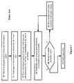
- FIG. 2shows a qualitative graph of the degradation of the grade of a data page (or block) of a memory device as a function of time, according to a preferred embodiment of the present invention.
- the grademay refer to a page or a block depending on the operation.
- the curves in FIG. 2represent the respective grades of pages or blocks of a memory device.
- the relative deteriorated health of the page/block of curve 30 at a given timeis shown as a grade difference 34 from curve 30 to line 32 .
- FIG. 3Ais a flowchart of the operational procedure for a method for monitoring the number of errors that were discovered and fixed by a memory controller, according to a preferred embodiment of the present invention.
- Informationis routinely read from the memory device, or access to the information is initiated by an application action or by an internal program running on the device's controller (e.g. an internal test or a regular maintenance procedure) (Block 40 ). While information is being read from the memory device, which includes reading the raw (i.e. originally-stored) data and any stored ECC information (Block 42 ), the information is checked for errors in the data (Block 44 ).
- the bits that do not match the raw dataare calculated (Block 44 ) and repaired (Block 46 ).
- the number of repaired bits per pageprovides the controller with a measure of the reliability of the currently-read page.
- the number of repaired bits per pageremains in the embedded controller (i.e. the controller embedded in the memory device), and only the corrected data is transferred to the application (Block 48 ).
- the repaired datais rewritten by the controller to the memory (Block 50 ).
- the controlleralso optionally stores the number of error bits as the measure of reliability of the page, known as the grade, to the memory (Block 52 ).
- FIG. 4Ais a simplified schematic diagram of the format of a typical data page, according to both the prior art and the present invention.
- a page 70typically has the ECC information, an ECC 72 , stored next to the relevant data, information data 74 .
- ECC 72is usually based on a known error detection/correction method (e.g. Reed-Salomon or BCH algorithm). Such correction algorithms can fix data to a limited level (e.g. up to four error bits per 512-byte page).
- a known error detection/correction methode.g. Reed-Salomon or BCH algorithm.
- Such correction algorithmscan fix data to a limited level (e.g. up to four error bits per 512-byte page).
- FIG. 4Bis a simplified schematic diagram of the format of a data page that includes a grade of the page, according to a preferred embodiment of the present invention.
- a page 76has a grade 78 stored next to ECC 72 and information data 74 .
- a typical report grade 78is one error bit per 512-byte page.
- grade 78increases to a dangerous level (e.g. four error bits per 512-byte page) or exceeds a threshold
- the applicationacts upon the information from grade 78 by initiating an action, even if information data 74 has been corrected. For example, the application can rewrite information data 74 to a different page, or report the deterioration, thereby enhancing the long-term reliability of information data 74 .
- FIG. 3Bis a flowchart of the operational procedure for a method for reporting the health of a memory device to a host system, according to a preferred embodiment of the present invention.
- a “page-error grade”is stored in the controller, and reported to the application in response to a read-operation (Block 54 ).
- a page grade or a dynamic (e.g. worst or average) grade found in the entire memoryis reported.
- the grade read-operationincludes the following steps.
- the host systemrequests either a particular page grade or a device grade (Block 56 ).
- the controllerthen reads the information from the information's stored location (e.g. memory, register, or embedded memory in the controller) (Block 58 ).
- the controllerperforms this calculation (Block 60 ).
- the requested informationi.e. the grade
- the host applicationBlock 62 ).
- FIG. 5is a flowchart of the operational procedure for a method for monitoring the number of pulses required for writing a page, and the number of bits that were flipped after a given number of pulses, according to a preferred embodiment of the present invention.
- the controlleruses the number of pulses required to set all of the bits to the correct values as a measure of the page deterioration.
- the procedure outlined in FIG. 5is similar to the procedure outlined in FIG. 1 .
- the datais stored in the memory buffer (Block 80 ), then the physical location in the memory for the write-operation is selected (Block 82 ).
- the first pulseis applied to program all bits (Block 84 ). After each programming pulse, the data is read, and compared with the target data in the buffer (Block 86 ).
- the number or percentage of bits in the page that are not successfully flipped by the first pulse or by any subsequent programming pulse(Block 88 ) is recorded. This number is used as an alternative measure of the memory aging or health.
- an additional counteris used, and is incremented after each pulse (Block 90 ). The counter counts the number of program pulses in the program cycle. The number of pulses required to complete the programming is used as a measure of the memory aging or health.
- the programmed bitsare checked to verify that they have met the threshold level (this level is higher than a standard read threshold-level) (Block 92 ). If not all of the bits are at the correct values (Block 92 ), an additional programming cycle is performed (Block 94 ). Optionally, the additional cycle may be performed with higher voltage (Block 94 ). When all of the bits match the buffer values, the program cycle (i.e. write-operation) is finished (Block 96 ).
- the reported gradeis a “block grade” (as opposed to a “page grade” ), and the information collected about the page grade from the read- and write-operations is used only to contribute information to the block grade for the specific block that contains the pages. As a result, the health is reported with a “block resolution” only.
- the reported graderepresents a deviation in power consumption (from a reference or initial power consumption, for example) of the device.
- a gradeindicates the efficiency of the device in executing the data operations. For example, a device which requires multiple programming pulses in order to perform an operation will consume more power than a device that can perform the operation with fewer pulses.
- a page that is not accessed for a given period of time, and therefore, the page's health has not been measured for a long period of timeis automatically read in background so that the aging of the page can be assessed.
- the aging of the deviceis evaluated by comparison of the measured health of the block/page to an original health after production (as stored in the original memory upon manufacture). This method compensates for inherent non-uniformity of the device, where some areas of the memory are produced with better health characteristics than other areas.
- FIG. 6Ais a high-level block diagram of a flash-memory device coupled to a host system, according to a preferred embodiment of the present invention.
- FIG. 6is adapted from FIG. 1 of Ban, U.S. Pat. No. 5,404,485, which patent is incorporated by reference for all purposes as if fully set forth herein (hereinafter referred to as Ban '485).
- a flash-memory device 100includes a flash memory 102 , a controller 104 , and a random-access memory (RAM) 106 .
- Controller 104which corresponds to “flash control 14 ” of Ban '485, manages flash memory 102 , with the help of RAM 106 , as described in Ban '485 and as described in U.S. Pat.
- Controller 104also supports refreshing of the data that are stored in flash memory 102 .
- Flash-memory device 100is shown connected to a host system 108 .
- FIG. 6Bis a high-level block diagram of an alternative flash-memory device coupled to a host system, according to a preferred embodiment of the present invention.
- Host system 110includes a processor 112 and four memory devices: a RAM 114 , a boot ROM 116 , a mass-storage device (e.g. hard disk) 118 and a flash memory device 120 , all communicating via a common bus 122 .
- flash-memory device 120includes flash memory 102 .
- flash-memory device 120lacks its controller and RAM.
- processor 112emulates controller 104 by executing a software driver (not shown) that implements the methodology of Ban '485 and Ban '425 (e.g. in the manner of the TrueFFSTM driver of msystems Ltd. of Kefar Saba, Israel), and that also implements the grade-monitoring methodology of the present invention.
- Flash-memory device 120also includes a bus interface 124 to enable processor 112 to communicate with flash memory 102 .
Landscapes
- Engineering & Computer Science (AREA)
- Theoretical Computer Science (AREA)
- Physics & Mathematics (AREA)
- General Engineering & Computer Science (AREA)
- General Physics & Mathematics (AREA)
- Software Systems (AREA)
- Techniques For Improving Reliability Of Storages (AREA)
- Read Only Memory (AREA)
- For Increasing The Reliability Of Semiconductor Memories (AREA)
Abstract
Description
This patent application claims the benefit of U.S. Provisional Patent Application No. 60/771,786 filed Feb. 10, 2006.
The present invention relates to methods for built-in detection of the deterioration of reliability in digital memory devices in general, and in removable flash-memory devices in particular.
Digital memory devices are often used as dependable memory devices for important data. As a result of the limited life expectancy and complexity of such equipment, digital memory devices can fail, and cause the loss of valuable data. Non-volatile storage systems include a memory and a control system, which sometimes reside on the same piece of silicon. One of the tasks performed by the control system is error correction.
Error-correction code (ECC) detects occasional errors in the data, generated by the storage element's nature or the characteristics of the operating environment, fixes the error, and delivers the corrected original information upon a user's request. The ECC system has a built-in limitation with regard to the number of errors that can be corrected. Upon encountering an excessive number of errors, the information cannot be repaired, and may be reported as lost, or may be sent with the errors to the user.
Software applications that use memory devices assume that the information is correct until the correction system fails to repair the data. As long as the memory is still fully functional, there is no indication to the user that the memory is deteriorating and approaching failure. It should be noted that the error level is only one of several early-warning symptoms that can be used to predict the life expectancy of a memory prior to failure.
Today, users (and applications) are unaware of the state, or condition, of the stored data. Thus, users are unable to take active measures to reduce the risk of losing data. Such measures include, for example, creating a back-up of the data, migrating the data to new storage media, and rewriting problematic areas of the memory device to other areas.
The current state of the art does not provide a way to report the “health” (i.e. operational-reliability performance) of a memory device. While some prior art methods record the usage of the device (i.e. the number of times the device is written to) for internal load-balancing purposes, the methods are not designed for the purpose of providing an early-warning indication to a user or application. While there is a correlation between the usage of the device and the device's remaining life expectancy, such a correlation is not absolute since there is a natural, random variability among devices (similar to the inaccuracy of predicting a person's life expectancy based on age only).
Methods that attempt to monitor the health of a memory device are known in the art, but are limited to programs that run on the host system. Thus, these methods can only deal with the corrected information, after error-correction methods have been employed to correct the errors. An example of a prior art system is provided in a feature called “Disk Health” that is included in the “Norton System Doctor (NSD)” product available from Symantec Corp., Cupertino, Calif. (also described in Document ID: 2001082218352309, included in the NSD product manual, and found on the Norton web site, www.norton.com). The data is read from the memory device; therefore, the host system is not exposed to the raw data before the data has been corrected. This aspect makes such prior-art methods less sensitive to early stages of deterioration in the health of the memory device.
It would be desirable to give the user of such memory devices an early-warning indication when the health of the device deteriorates and approaches a high probability of failure.
It would be further desirable to have a system, operating according to a method, which resides on a memory device, and detects and reports the actual deterioration of indicative longevity parameters on the memory device before any attempt is made to correct the data. Such a system would be of significant importance for modern multi-level flash-memory devices in which the inherent life expectancy is shorter than in traditional single-level flash-memory devices, and in which the symptoms of aging can be measured without slowing the routine operation.
It is the purpose of the present invention to provide methods for built-in detection of the deterioration of reliability in digital memory devices in general, and in removable flash-memory devices in particular. The present invention describes flash-memory devices as a typical example, but is applicable to, and intended to cover, any memory device.
For the purpose of clarity, several terms which follow are specifically defined for use within the context of this application. The term “longevity parameter” is used in this application to refer to a variable of a memory device whose value changes during the life of the memory device, represents a relative deteriorated health of at least one cell of the memory device, and correlates with the device's life expectancy. Such parameters include, for example: the average number of errors, the number of programming cycles, and the number of bits that flipped logic state (upon the first programming pulse of a programming operation) when the bits are written to the memory.
The present invention applies to both single-level-cell (SLC) flash memories and multi-level-cell (MLC) flash memories. While the subsequent discussion focuses primarily on SLC cells, it will be clear to those skilled in the art how the present invention applies to MLC cells. The terms “erasing” and “writing” are used herein to refer to setting threshold voltages of a memory cell, where erasing typically sets the voltages to correspond to one-logic states, and writing typically sets the voltages to correspond to zero-logic states for SLC cells. The terms “writing” and “programming” are used interchangeably herein. The present invention is particularly applicable to NAND-type flash memories that are read and programmed a page at a time.
The term “block” is used in this application to refer to the smallest number of cells, in a memory, that can be erased in a single operation. The term “page” is used in this application to refer to the smallest number of cells, in a memory, that that can be written in a single operation. Typically, there are multiple pages in a block. The term “grade” is used in this application to refer to a measure of the reliability of a memory page or block based on the values of the page's or block's longevity parameters. It is noted that an erase-operation is typically performed on a block (as opposed to a page). Thus, in the context of erase-operations, the grade refers to a measure of the reliability of a block based on the block's longevity parameters.
The term “initial health” is used in this application to refer to a longevity parameter that represents the deviation of the grade of a page or block from some reference value. Blocks can start their “lives” with different initial healths. The term “relative deteriorated health” is used in this application to refer to the deterioration of the health of a block or page from an initial health since the block was produced and tested. The health of blocks can deteriorate at different rates. The term “healthy cells” is used in this application to refer to cells that have successfully changed logic states after a sequence of programming pulses associated with a data operation.
Furthermore, the term “memory device” is used in this application to refer to any non-volatile memory that stores data via a physical process that can result in errors. Such memory devices include portable and stationary devices, based on semiconductor, magnetic, holographic, optical, and other physical binary-logic memory-technologies.
Usually, the programming cycles utilize gradually increasing levels of voltage until the end of the write-operation. However, in some types of NAND-type flash-memory devices, the difference between the first and second pulses is much higher than the subsequent pulses. In such a case, an option to increase the voltage in small steps after a few initial large increments is utilized.
The process of selectively writing (i.e. programming) data to a flash memory involves changing logic states of selected memory cells, typically, in a SLC implementation, from one-logic to zero-logic. The process of selectively erasing data from a flash memory involves changing values of selected memory cells, typically from zero-logic to one-logic. However, this designation is arbitrary, and would be equally implementable in the opposite designation.
NAND-type flash memories have one or more page buffers (i.e. memory cells with read/write capability), which receive the data before the data is programmed into the flash memory cells. Page-programming methods, for flash memory in which each flash memory cell contains one bit of information and erased flash memory cells have one-logic, implement the following steps:
- (1) Apply a programming voltage pulse only to flash memory cells that have zero-logic in the corresponding cells of the page buffer, where a programming voltage pulse is a single attempt to set a cell to the desired threshold voltage, typically many such pulses are required to achieve the required voltage level;
- (2) Read the data programmed into the memory;
- (3) Set the corresponding cells of the page buffer to one-logic for all flash memory cells that return zero-logic when read;
- (4) Repeat steps 1-3 until all cells in the page buffer contain one-logic or until the number of pulses exceeds the maximum number allowed; and
- (5) If the number of pulses exceeds the maximum number allowed, then return a failure status for the page-programming operation.
The present invention includes several preferred embodiments in which the memory controller of a flash-memory device can detect symptoms of deterioration in the flash-memory device, and provide a reliable prediction of the life expectancy of the flash-memory device. A longevity parameter, derived from a grade, serves as a “forecast” of the life expectancy of the flash-memory device. A device having a poorer longevity parameter is indicative of a relatively shorter life expectancy than a device with a better longevity parameter.
In a preferred embodiment, the system monitors the probability of error in reading data from the flash memory. Usually, this statistic is available to the ECC of the flash-memory controller, and does not require any direct access to the flash memory itself. In some flash-memory devices, the ECC is built into the flash memory itself. In such devices, information about the number of errors is made available to the memory controller by a command.
In another preferred embodiment, the system monitors either the average or the maximum number of pulses required to change the state of a data bit during programming. In flash-memory devices, this number typically ranges from 4 to 25 programming pulses (depending on the type of flash memory). As the flash memory deteriorates, the number of pulses required to write the data to the flash memory increases.
In another preferred embodiment, the system monitors the number of successful changes of logic state of data bits after a given number of pulses. For example, the numbers of bits that are correctly programmed after the first pulse decreases with the deterioration of the flash memory as more bits require more than one pulse for writing.
Therefore, according to the present invention, there is provided for the first time a method for managing a memory device, the method including: (a) monitoring a value of a longevity parameter of the memory device after a data operation on the memory device, the monitoring being performed by the memory device; and (b) deriving a grade of the memory device from the value.
Preferably, the longevity parameter is a ratio of successfully-processed data to unsuccessfully-processed data.
Alternatively, the longevity parameter is a deviation in a power consumption of the memory device. Most preferably, the deviation is an average of measurements for a plurality of the operations.
Preferably, the grade serves as a forecast of a life expectancy of the memory.
Preferably, the operation is a programming operation, and the value is a number of programming pulses, associated with the operation, required to change logic states of at least one cell in a page of the memory device.
Preferably, the operation is an erase operation, and the value is a number of programming pulses, associated with the operation, required to change logic states of at least one cell in a block of the memory device.
Preferably, the operation is a programming operation, and the value is a number of healthy cells in a page of the memory device.
Preferably, the operation is an erase operation, and the value is a number of healthy cells in a block of the memory device.
Preferably, the operation is selected from the group consisting of: writing data, reading data, and erasing data.
Preferably, the grade is selected from the group consisting of: a comparison grade of a current value to a pre-determined reference value, a maximum grade of a plurality of the values stored in a monitoring device, and an average grade of the plurality of the values stored in the monitoring device.
Most preferably, if the grade is a comparison of a current value to a pre-determined reference value, the method further includes the step of: (c) storing the pre-determined reference value in the memory device upon manufacture of the memory device.
Preferably, the step of monitoring includes accessing the memory device for the purpose of deriving the grade.
Preferably, the method further includes the step of: (c) storing the grade in a monitoring device.
Most preferably, the monitoring device is selected from the group consisting of: the memory device, an embedded controller of the memory device, and a host system of the memory device.
Preferably, the step of deriving is initiated by the memory device.
Preferably, the step of deriving is initiated by a host system of the memory device.
Preferably, the step of deriving is initiated by an embedded controller of the memory device.
Preferably, the step of deriving is initiated by an application running on a host system.
Preferably, the step of deriving is initiated by an operating system running on a host system.
According to the present invention, there is provided for the first time a memory device for managing data, the device including: (a) a memory; and (b) a controller operative: (i) to monitor a value of a longevity parameter after a data operation on the memory; and (ii) to derive a grade of the memory device from the value.
Preferably, the grade serves as a forecast of a life expectancy of the memory device.
According to the present invention, there is provided for the first time a system for managing data, the system including: (a) a memory device including a memory; and (b) a processor, housed in said memory device, operative: (i) to monitor a value of a longevity parameter after a data operation on the memory; and (ii) to derive a grade of the memory device from the value.
Preferably, the grade serves as a forecast of a life expectancy of the memory device.
These and further embodiments will be apparent from the detailed description and examples that follow.
The present invention is herein described, by way of example only, with reference to the accompanying drawings, wherein:
The present invention relates to methods for built-in detection of the deterioration of reliability in digital memory devices. The principles and operation for built-in detection of the deterioration of reliability in digital memory devices, according to the present invention, may be better understood with reference to the accompanying description and the drawings.
Referring now to the drawings,FIG. 2 shows a qualitative graph of the degradation of the grade of a data page (or block) of a memory device as a function of time, according to a preferred embodiment of the present invention. As noted above, the grade may refer to a page or a block depending on the operation. The curves inFIG. 2 represent the respective grades of pages or blocks of a memory device. Consider onesuch curve 30. The initial health of the page/block ofcurve 30 is defined as the deviation of the initial grade of curve30 (at t =0, i.e. at production/testing of the memory) from a reference grade value, shown as aline 32. The relative deteriorated health of the page/block ofcurve 30 at a given time is shown as agrade difference 34 fromcurve 30 toline 32.
While the error detection/correction is employed, errors are fixed. The bits that do not match the raw data are calculated (Block44) and repaired (Block46). The number of repaired bits per page provides the controller with a measure of the reliability of the currently-read page. In the present embodiment, the number of repaired bits per page remains in the embedded controller (i.e. the controller embedded in the memory device), and only the corrected data is transferred to the application (Block48). Optionally, in some ECC algorithms, the repaired data is rewritten by the controller to the memory (Block50). Furthermore, the controller also optionally stores the number of error bits as the measure of reliability of the page, known as the grade, to the memory (Block52).
Alternatively, a different type of grade reporting can be employed.FIG. 3B is a flowchart of the operational procedure for a method for reporting the health of a memory device to a host system, according to a preferred embodiment of the present invention. In the present embodiment, a “page-error grade” is stored in the controller, and reported to the application in response to a read-operation (Block54). In response to a direct request from the application (Block54), either a page grade or a dynamic (e.g. worst or average) grade found in the entire memory is reported. In the case of a dynamic grade representing a worst grade, this grade is updated each time the data is read if the number of errors exceeds the currently-stored grade, so that the grade shows the maximum number of errors detected for the page or for the entire memory device. In the case of a dynamic grade representing an average grade, this grade is updated each time the data is read. The grade read-operation (Block54) includes the following steps. The host system requests either a particular page grade or a device grade (Block56). The controller then reads the information from the information's stored location (e.g. memory, register, or embedded memory in the controller) (Block58).
Optionally, if the action requires calculation of a grade based on the stored grade (e.g. an average or maximum of all pages based on the pages' individual grades), the controller performs this calculation (Block60). The requested information (i.e. the grade) is then sent to the host application (Block62).
In a preferred embodiment, the number or percentage of bits in the page that are not successfully flipped by the first pulse or by any subsequent programming pulse (Block88) is recorded. This number is used as an alternative measure of the memory aging or health. In another preferred embodiment, alternatively or additionally to the step ofBlock 88, an additional counter is used, and is incremented after each pulse (Block90). The counter counts the number of program pulses in the program cycle. The number of pulses required to complete the programming is used as a measure of the memory aging or health.
After each programming cycle, the programmed bits are checked to verify that they have met the threshold level (this level is higher than a standard read threshold-level) (Block92). If not all of the bits are at the correct values (Block92), an additional programming cycle is performed (Block94). Optionally, the additional cycle may be performed with higher voltage (Block94). When all of the bits match the buffer values, the program cycle (i.e. write-operation) is finished (Block96).
In a preferred embodiment of the present invention, the reported grade is a “block grade” (as opposed to a “page grade” ), and the information collected about the page grade from the read- and write-operations is used only to contribute information to the block grade for the specific block that contains the pages. As a result, the health is reported with a “block resolution” only.
In a preferred embodiment of the present invention, the reported grade represents a deviation in power consumption (from a reference or initial power consumption, for example) of the device. Such a grade indicates the efficiency of the device in executing the data operations. For example, a device which requires multiple programming pulses in order to perform an operation will consume more power than a device that can perform the operation with fewer pulses.
In a preferred embodiment of the present invention, a page that is not accessed for a given period of time, and therefore, the page's health has not been measured for a long period of time, is automatically read in background so that the aging of the page can be assessed.
In another preferred embodiment of the present invention, the aging of the device is evaluated by comparison of the measured health of the block/page to an original health after production (as stored in the original memory upon manufacture). This method compensates for inherent non-uniformity of the device, where some areas of the memory are produced with better health characteristics than other areas.
While the invention has been described with respect to a limited number of embodiments, it will be appreciated that many variations, modifications, and other applications of the invention may be made.
Claims (34)
1. A method for managing a memory device, the method comprising the steps of:
(a) monitoring a value of a longevity parameter of the memory device after a programming operation on the memory device, said monitoring being performed by the memory device; and
(b) deriving a grade of the memory device from said value;
wherein said value is a number of programming pulses, associated with said operation, required to change logic states of at least one cell in a page of the memory device.
2. The method ofclaim 1 , wherein said longevity parameter is a ratio of successfully-processed data to unsuccessfully-processed data.
3. The method ofclaim 1 , wherein said longevity parameter is a deviation in a power consumption of the memory device.
4. The method ofclaim 1 , wherein said deviation is an average of measurements for a plurality of said operations.
5. The method ofclaim 1 , wherein said grade serves as a forecast of a life expectancy of said memory.
6. The method ofclaim 1 , wherein said operation is a programming operation, and wherein said value is a number of healthy cells in a page of the memory device.
7. The method ofclaim 1 , wherein said operation is an erase operation, and wherein said value is a number of healthy cells in a block of the memory device.
8. The method ofclaim 1 , wherein said operation is selected from the group consisting of: writing data, reading data, and erasing data.
9. The method ofclaim 1 , wherein said grade is selected from the group consisting of: a comparison grade of a current said value to a pre-determined reference said value, a maximum grade of a plurality of said values stored in a monitoring device, and an average grade of said plurality of said values stored in said monitoring device.
10. The method ofclaim 1 , wherein said grade is a comparison grade of a current value to a pre-determined reference value, the method further comprising the step of:
(c) storing said pre-determined reference value in the memory device upon manufacture of the memory device.
11. The method ofclaim 1 , wherein said step of monitoring includes accessing the memory device for the purpose of deriving said grade.
12. The method ofclaim 1 , the method further comprising the step of:
(c) storing said grade in a monitoring device.
13. The method ofclaim 12 , wherein said monitoring device is selected from the group consisting of: the memory device, an embedded controller of the memory device, and a host system of the memory device.
14. The method ofclaim 1 , wherein said step of deriving is initiated by the memory device.
15. The method ofclaim 1 , wherein said step of deriving is initiated by a host system of the memory device.
16. The method ofclaim 1 , wherein said step of deriving is initiated by an embedded controller of the memory device.
17. The method ofclaim 1 , wherein said step of deriving is initiated by an application running on a host system.
18. The method ofclaim 1 , wherein said step of deriving is initiated by an operating system running on a host system.
19. A memory device for managing data, the device comprising:
(a) a memory; and
(b) a controller operative:
(i) to monitor a value of a longevity parameter after a programming operation on said memory; and
(ii) to derive a grade of the memory device from said value;
wherein said value is a number of programming pulses associated with said operation required to change logic states of at least one cell in a page of the memory device.
20. The memory device ofclaim 19 , wherein said grade serves as a forecast of a life expectancy of the memory device.
21. A system for managing data, the system comprising:
(a) a memory device including a memory; and
(b) a processor, housed in said memory device, operative:
(i) to monitor a value of a longevity parameter after a programming operation on said memory; and
(ii) to derive a grade of said memory device from said value;
wherein said value is a number of programming pulses, associated with said operation, required to change logic states of at least one cell in a page of the memory device.
22. The system ofclaim 21 , wherein said grade serves as a forecast of a life expectancy of said memory device.
23. A method for managing a memory device, the method comprising the steps of:
(a) monitoring a value of a longevity parameter of the memory device after an erase operation on the memory device, said monitoring being performed by the memory device; and
(b) deriving a grade of the memory device from said value;
wherein said value is a number of programming pulses, associated with said operation, required to change logic states of at least one cell in a block of the memory device.
24. A memory device for managing data, the device comprising:
(a) a memory; and
(b) a controller operative:
(i) to monitor a value of a longevity parameter after an erase operation on said memory; and
(ii) to derive a grade of the memory device from said value;
wherein said value is a number of programming pulses, associated with said operation, required to change logic states of at least one cell in a block of the memory device.
25. A system for managing data, the system comprising:
(a) a memory device including a memory; and
(b) a processor, housed in said memory device, operative:
(i) to monitor a value of a longevity parameter after an erase operation on said memory; and
(ii) to derive a grade of said memory device from said value;
wherein said value is a number of programming pulses, associated with said operation, required to change logic states of at least one cell in a block of the memory device.
26. A method for managing a memory device, the method comprising the steps of:
(a) monitoring a value of a deviation in a power consumption of the memory device after a data operation on the memory device, said monitoring being performed by the memory device; and
(b) deriving a grade of the memory device from said value.
27. The method ofclaim 26 , wherein the memory device is a flash memory device.
28. A memory device for managing data, the device comprising:
(a) a memory; and
(b) a controller operative:
(i) to monitor a value of a deviation in a power consumption of the memory device after a data operation on said memory; and
(ii) to derive a grade of the memory device from said value.
29. The method ofclaim 28 , wherein said memory is a flash memory.
30. A system for managing data, the system comprising:
(a) a memory device including a memory; and
(b) a processor, housed in said memory device, operative:
(i) to monitor a value of a deviation in a power consumption of the memory device after a data operation on said memory; and
(ii) to derive a grade of said memory device from said value.
31. The method ofclaim 30 , wherein said memory device is a flash memory device.
32. A method for managing a memory device, the method comprising the steps of:
(a) monitoring a number of healthy cells in a block of the memory device after an erase operation on the memory device, said monitoring being performed by the memory device; and
(b) deriving a grade of the memory device from said value.
33. A memory device for managing data, the device comprising:
(a) a memory; and
(b) a controller operative:
(i) to monitor a number of healthy cells in a block of said memory after an erase operation on said memory; and
(ii) to derive a grade of the memory device from said value.
34. A system for managing data, the system comprising:
(a) a memory device including a memory; and
(b) a processor, housed in said memory device, operative:
(i) to monitor a number of healthy cells in a block of said memory after an erase operation on said memory; and
(ii) to derive a grade of said memory device from said value.
Priority Applications (1)
| Application Number | Priority Date | Filing Date | Title |
|---|---|---|---|
| US11/702,500US7512847B2 (en) | 2006-02-10 | 2007-02-06 | Method for estimating and reporting the life expectancy of flash-disk memory |
Applications Claiming Priority (2)
| Application Number | Priority Date | Filing Date | Title |
|---|---|---|---|
| US77178606P | 2006-02-10 | 2006-02-10 | |
| US11/702,500US7512847B2 (en) | 2006-02-10 | 2007-02-06 | Method for estimating and reporting the life expectancy of flash-disk memory |
Publications (2)
| Publication Number | Publication Date |
|---|---|
| US20070198786A1 US20070198786A1 (en) | 2007-08-23 |
| US7512847B2true US7512847B2 (en) | 2009-03-31 |
Family
ID=38345543
Family Applications (1)
| Application Number | Title | Priority Date | Filing Date |
|---|---|---|---|
| US11/702,500Active2027-05-02US7512847B2 (en) | 2006-02-10 | 2007-02-06 | Method for estimating and reporting the life expectancy of flash-disk memory |
Country Status (7)
| Country | Link |
|---|---|
| US (1) | US7512847B2 (en) |
| EP (1) | EP1982264A2 (en) |
| JP (1) | JP2009526340A (en) |
| KR (1) | KR101348665B1 (en) |
| CN (1) | CN101529526B (en) |
| TW (1) | TWI339337B (en) |
| WO (1) | WO2007091263A2 (en) |
Cited By (36)
| Publication number | Priority date | Publication date | Assignee | Title |
|---|---|---|---|---|
| US20070180328A1 (en)* | 2006-01-27 | 2007-08-02 | Cornwell Michael J | Monitoring health of non-volatile memory |
| US20080288712A1 (en)* | 2007-04-25 | 2008-11-20 | Cornwell Michael J | Accessing metadata with an external host |
| US20090313444A1 (en)* | 2006-06-28 | 2009-12-17 | Seiko Epson Corporation | Semiconductor storage apparatus managing system, semiconductor storage apparatus, host apparatus, program and method of managing semiconductor storage apparatus |
| US20100011260A1 (en)* | 2006-11-30 | 2010-01-14 | Kabushiki Kaisha Toshiba | Memory system |
| US20100153352A1 (en)* | 2008-12-16 | 2010-06-17 | Judah Gamliel Hahn | Discardable files |
| US20100153474A1 (en)* | 2008-12-16 | 2010-06-17 | Sandisk Il Ltd. | Discardable files |
| US20100153452A1 (en)* | 2008-12-16 | 2010-06-17 | Judah Gamliel Hahn | Discardable files |
| US20100162012A1 (en)* | 2006-01-25 | 2010-06-24 | Apple Inc. | Reporting flash memory operating voltages |
| US20100180091A1 (en)* | 2008-12-16 | 2010-07-15 | Judah Gamliel Hahn | Discardable files |
| US20100235473A1 (en)* | 2009-03-10 | 2010-09-16 | Sandisk Il Ltd. | System and method of embedding second content in first content |
| US20100306451A1 (en)* | 2009-06-01 | 2010-12-02 | Joshua Johnson | Architecture for nand flash constraint enforcement |
| US20100306581A1 (en)* | 2009-06-01 | 2010-12-02 | Lsi Corporation | Solid state storage end of life prediction with correction history |
| US20100313100A1 (en)* | 2009-06-04 | 2010-12-09 | Lsi Corporation | Flash Memory Organization |
| US20100313097A1 (en)* | 2009-06-04 | 2010-12-09 | Lsi Corporation | Flash Memory Organization |
| US20110022779A1 (en)* | 2009-07-24 | 2011-01-27 | Lsi Corporation | Skip Operations for Solid State Disks |
| US7913032B1 (en) | 2007-04-25 | 2011-03-22 | Apple Inc. | Initiating memory wear leveling |
| US20110072198A1 (en)* | 2009-09-23 | 2011-03-24 | Lsi Corporation | Accessing logical-to-physical address translation data for solid state disks |
| US20110087898A1 (en)* | 2009-10-09 | 2011-04-14 | Lsi Corporation | Saving encryption keys in one-time programmable memory |
| US20110131375A1 (en)* | 2009-11-30 | 2011-06-02 | Noeldner David R | Command Tag Checking in a Multi-Initiator Media Controller Architecture |
| US20110161552A1 (en)* | 2009-12-30 | 2011-06-30 | Lsi Corporation | Command Tracking for Direct Access Block Storage Devices |
| US20110239061A1 (en)* | 2007-06-07 | 2011-09-29 | Micron Technology, Inc. | Systems and methods for retrieving data |
| US20110289380A1 (en)* | 2010-05-21 | 2011-11-24 | Wilkerson Christopher B | Method and apparatus for using cache memory in a system that supports a low power state |
| US8463802B2 (en) | 2010-08-19 | 2013-06-11 | Sandisk Il Ltd. | Card-based management of discardable files |
| US8549229B2 (en) | 2010-08-19 | 2013-10-01 | Sandisk Il Ltd. | Systems and methods for managing an upload of files in a shared cache storage system |
| US8755229B1 (en) | 2009-06-23 | 2014-06-17 | Micron Technology, Inc. | Limiting flash memory over programming |
| US8788849B2 (en) | 2011-02-28 | 2014-07-22 | Sandisk Technologies Inc. | Method and apparatus for protecting cached streams |
| US9015209B2 (en) | 2008-12-16 | 2015-04-21 | Sandisk Il Ltd. | Download management of discardable files |
| US9020993B2 (en) | 2008-12-16 | 2015-04-28 | Sandisk Il Ltd. | Download management of discardable files |
| US20150178150A1 (en)* | 2013-12-20 | 2015-06-25 | Netapp, Inc. | Techniques for Assessing Pass/Fail Status of Non-Volatile Memory |
| US9104686B2 (en) | 2008-12-16 | 2015-08-11 | Sandisk Technologies Inc. | System and method for host management of discardable objects |
| US9146855B2 (en) | 2012-01-09 | 2015-09-29 | Dell Products Lp | Systems and methods for tracking and managing non-volatile memory wear |
| US9292473B2 (en) | 2012-12-28 | 2016-03-22 | International Business Machines Corporation | Predicting a time of failure of a device |
| KR20170031052A (en)* | 2015-09-04 | 2017-03-20 | 에이취지에스티 네덜란드 비.브이. | Wear management for flash memory devices |
| US9798475B2 (en) | 2015-03-11 | 2017-10-24 | Toshiba Memory Corporation | Memory system and method of controlling nonvolatile memory |
| US10108354B2 (en) | 2014-05-20 | 2018-10-23 | Samsung Electronics Co., Ltd. | Memory controller operation |
| US10235056B2 (en) | 2014-09-26 | 2019-03-19 | Western Digital Technologies, Inc. | Storage device health diagnosis |
Families Citing this family (36)
| Publication number | Priority date | Publication date | Assignee | Title |
|---|---|---|---|---|
| US7616508B1 (en)* | 2006-08-10 | 2009-11-10 | Actel Corporation | Flash-based FPGA with secure reprogramming |
| TWI362044B (en) | 2007-11-09 | 2012-04-11 | Transcend Information Inc | Storage apparatus and method for accessing data and for managing memory block |
| US7903486B2 (en)* | 2007-11-19 | 2011-03-08 | Sandforce, Inc. | System, method, and computer program product for increasing a lifetime of a plurality of blocks of memory |
| US20090161243A1 (en)* | 2007-12-21 | 2009-06-25 | Ratnesh Sharma | Monitoring Disk Drives To Predict Failure |
| TWI381391B (en)* | 2008-08-05 | 2013-01-01 | Transcend Information Inc | Storage device with self-condition inspection and inspecting method thereof |
| CN101685675B (en)* | 2008-09-26 | 2014-01-15 | 美光科技公司 | Operation of memory unit |
| US7996725B2 (en)* | 2008-11-14 | 2011-08-09 | Nokia Corporation | Providing protection for a memory device |
| JP5544712B2 (en)* | 2008-12-26 | 2014-07-09 | 富士通株式会社 | Memory lifetime detection apparatus and method |
| US8380946B2 (en)* | 2009-04-08 | 2013-02-19 | International Business Machines Corporation | System, method, and computer program product for estimating when a reliable life of a memory device having finite endurance and/or retention, or portion thereof, will be expended |
| US8321727B2 (en)* | 2009-06-29 | 2012-11-27 | Sandisk Technologies Inc. | System and method responsive to a rate of change of a performance parameter of a memory |
| US8400854B2 (en)* | 2009-09-11 | 2013-03-19 | Sandisk Technologies Inc. | Identifying at-risk data in non-volatile storage |
| JP2012027964A (en)* | 2010-07-20 | 2012-02-09 | Panasonic Corp | Memory device and cpu control method |
| US8422303B2 (en)* | 2010-12-22 | 2013-04-16 | HGST Netherlands B.V. | Early degradation detection in flash memory using test cells |
| JP5604313B2 (en)* | 2011-01-12 | 2014-10-08 | 株式会社メガチップス | Memory access control device |
| US8560922B2 (en) | 2011-03-04 | 2013-10-15 | International Business Machines Corporation | Bad block management for flash memory |
| CN102163165B (en)* | 2011-05-26 | 2012-11-14 | 忆正存储技术(武汉)有限公司 | Error estimation module and estimation method thereof for flash memory |
| US10359949B2 (en)* | 2011-10-31 | 2019-07-23 | Apple Inc. | Systems and methods for obtaining and using nonvolatile memory health information |
| CN103325424A (en)* | 2012-03-23 | 2013-09-25 | 绿智慧流科技公司 | Method for evaluating lifetime of flash memory |
| DE102012024772A1 (en)* | 2012-12-18 | 2014-06-18 | Giesecke & Devrient Gmbh | Method for operating a subscriber identification module and such a subscriber identification module |
| US10083069B2 (en) | 2013-06-27 | 2018-09-25 | Sandisk Technologies Llc | Word line defect detection and handling for a data storage device |
| CN103577337B (en)* | 2013-11-05 | 2017-02-22 | 华为技术有限公司 | Space allocation method and device for storage system |
| CN103713857B (en)* | 2013-12-24 | 2017-06-27 | 华为技术有限公司 | Method and storage device for storing data |
| KR20150112075A (en)* | 2014-03-26 | 2015-10-07 | 삼성전자주식회사 | Storage device and operating method of storage device |
| CN104464809A (en)* | 2014-11-05 | 2015-03-25 | 武汉新芯集成电路制造有限公司 | Method for prolonging service life of flash memory |
| CN106297898A (en)* | 2015-06-03 | 2017-01-04 | 杭州海康威视数字技术股份有限公司 | The life-span method for early warning of a kind of NAND flash storage and device |
| CN106779008A (en)* | 2015-11-23 | 2017-05-31 | 杭州海康威视数字技术股份有限公司 | SD card, video camera and SD card reliability early warning system |
| CN107346668B (en)* | 2017-07-12 | 2020-08-21 | 武汉新芯集成电路制造有限公司 | Durability test method |
| US11016693B2 (en) | 2018-06-21 | 2021-05-25 | International Business Machines Corporation | Block health estimation for wear leveling in non-volatile memories |
| WO2021040810A1 (en)* | 2019-08-23 | 2021-03-04 | Futurewei Technologies, Inc. | Device lifetime prediction |
| CN111240887A (en)* | 2020-01-07 | 2020-06-05 | 苏州大学 | Error page identification method based on three-dimensional flash memory storage structure |
| CN115298652A (en)* | 2020-04-30 | 2022-11-04 | 北京嘀嘀无限科技发展有限公司 | System and method for storage medium health assessment |
| CN112379832B (en)* | 2020-11-05 | 2023-04-25 | 杭州海康威视数字技术股份有限公司 | Storage medium detection method and device |
| JP2023079292A (en)* | 2021-11-29 | 2023-06-08 | ラピステクノロジー株式会社 | Semiconductor storage device, data writing method, and manufacturing method of semiconductor storage device |
| KR102689776B1 (en)* | 2022-02-14 | 2024-07-29 | 백석대학교산학협력단 | A method for predicting life of flash memory-based storage using gradient descent and the system thereof |
| US20240345932A1 (en)* | 2023-04-17 | 2024-10-17 | Micron Technology, Inc. | Memory device health monitoring logic |
| CN116737515B (en)* | 2023-05-10 | 2024-02-23 | 珠海妙存科技有限公司 | Flash memory parameter visualization method, system and storage medium |
Citations (12)
| Publication number | Priority date | Publication date | Assignee | Title |
|---|---|---|---|---|
| US5404485A (en) | 1993-03-08 | 1995-04-04 | M-Systems Flash Disk Pioneers Ltd. | Flash file system |
| US5537357A (en)* | 1994-06-27 | 1996-07-16 | Intel Corporation | Method for preconditioning a nonvolatile memory array |
| US5959891A (en)* | 1996-08-16 | 1999-09-28 | Altera Corporation | Evaluation of memory cell characteristics |
| US6119245A (en)* | 1997-08-06 | 2000-09-12 | Oki Electric Industry Co., Ltd. | Semiconductor storage device and method of controlling it |
| US20030023911A1 (en)* | 2001-07-25 | 2003-01-30 | Davis James Andrew | Method for error correction decoding in an MRAM device (historical erasures) |
| US20040088614A1 (en)* | 2002-11-01 | 2004-05-06 | Ting-Chin Wu | Management system for defective memory |
| US6948102B2 (en)* | 2002-04-29 | 2005-09-20 | International Business Machines Corporation | Predictive failure analysis for storage networks |
| US20060236165A1 (en)* | 2005-03-21 | 2006-10-19 | Cepulis Darren J | Managing memory health |
| US20070067678A1 (en)* | 2005-07-11 | 2007-03-22 | Martin Hosek | Intelligent condition-monitoring and fault diagnostic system for predictive maintenance |
| US20070150689A1 (en)* | 2005-12-22 | 2007-06-28 | Pandit Anil K | Effective wear-leveling and concurrent reclamation method for embedded linear flash file systems |
| US20070180328A1 (en)* | 2006-01-27 | 2007-08-02 | Cornwell Michael J | Monitoring health of non-volatile memory |
| US7277336B2 (en)* | 2004-12-28 | 2007-10-02 | Sandisk 3D Llc | Method and apparatus for improving yield in semiconductor devices by guaranteeing health of redundancy information |
Family Cites Families (2)
| Publication number | Priority date | Publication date | Assignee | Title |
|---|---|---|---|---|
| GB2300946B (en)* | 1995-05-17 | 1999-10-20 | Altera Corp | Tri-statable input/output circuitry for programmable logic |
| KR100468616B1 (en)* | 2004-03-02 | 2005-01-31 | 주식회사 하이스마텍 | System and method for extending the lifetime of a nonvolatile memory |
- 2007
- 2007-02-06USUS11/702,500patent/US7512847B2/enactiveActive
- 2007-02-08JPJP2008553887Apatent/JP2009526340A/enactivePending
- 2007-02-08KRKR1020087018661Apatent/KR101348665B1/ennot_activeExpired - Fee Related
- 2007-02-08CNCN2007800036139Apatent/CN101529526B/enactiveActive
- 2007-02-08WOPCT/IL2007/000173patent/WO2007091263A2/enactiveApplication Filing
- 2007-02-08EPEP07706116Apatent/EP1982264A2/ennot_activeWithdrawn
- 2007-02-09TWTW096104903Apatent/TWI339337B/ennot_activeIP Right Cessation
Patent Citations (12)
| Publication number | Priority date | Publication date | Assignee | Title |
|---|---|---|---|---|
| US5404485A (en) | 1993-03-08 | 1995-04-04 | M-Systems Flash Disk Pioneers Ltd. | Flash file system |
| US5537357A (en)* | 1994-06-27 | 1996-07-16 | Intel Corporation | Method for preconditioning a nonvolatile memory array |
| US5959891A (en)* | 1996-08-16 | 1999-09-28 | Altera Corporation | Evaluation of memory cell characteristics |
| US6119245A (en)* | 1997-08-06 | 2000-09-12 | Oki Electric Industry Co., Ltd. | Semiconductor storage device and method of controlling it |
| US20030023911A1 (en)* | 2001-07-25 | 2003-01-30 | Davis James Andrew | Method for error correction decoding in an MRAM device (historical erasures) |
| US6948102B2 (en)* | 2002-04-29 | 2005-09-20 | International Business Machines Corporation | Predictive failure analysis for storage networks |
| US20040088614A1 (en)* | 2002-11-01 | 2004-05-06 | Ting-Chin Wu | Management system for defective memory |
| US7277336B2 (en)* | 2004-12-28 | 2007-10-02 | Sandisk 3D Llc | Method and apparatus for improving yield in semiconductor devices by guaranteeing health of redundancy information |
| US20060236165A1 (en)* | 2005-03-21 | 2006-10-19 | Cepulis Darren J | Managing memory health |
| US20070067678A1 (en)* | 2005-07-11 | 2007-03-22 | Martin Hosek | Intelligent condition-monitoring and fault diagnostic system for predictive maintenance |
| US20070150689A1 (en)* | 2005-12-22 | 2007-06-28 | Pandit Anil K | Effective wear-leveling and concurrent reclamation method for embedded linear flash file systems |
| US20070180328A1 (en)* | 2006-01-27 | 2007-08-02 | Cornwell Michael J | Monitoring health of non-volatile memory |
Cited By (90)
| Publication number | Priority date | Publication date | Assignee | Title |
|---|---|---|---|---|
| US20100162012A1 (en)* | 2006-01-25 | 2010-06-24 | Apple Inc. | Reporting flash memory operating voltages |
| US8171318B2 (en) | 2006-01-25 | 2012-05-01 | Apple Inc. | Reporting flash memory operating voltages |
| US20070180328A1 (en)* | 2006-01-27 | 2007-08-02 | Cornwell Michael J | Monitoring health of non-volatile memory |
| US7861122B2 (en)* | 2006-01-27 | 2010-12-28 | Apple Inc. | Monitoring health of non-volatile memory |
| US7962807B2 (en)* | 2006-06-28 | 2011-06-14 | Seiko Epson Corporation | Semiconductor storage apparatus managing system, semiconductor storage apparatus, host apparatus, program and method of managing semiconductor storage apparatus |
| US20090313444A1 (en)* | 2006-06-28 | 2009-12-17 | Seiko Epson Corporation | Semiconductor storage apparatus managing system, semiconductor storage apparatus, host apparatus, program and method of managing semiconductor storage apparatus |
| US20100011260A1 (en)* | 2006-11-30 | 2010-01-14 | Kabushiki Kaisha Toshiba | Memory system |
| US8156393B2 (en)* | 2006-11-30 | 2012-04-10 | Kabushiki Kaisha Toshiba | Memory system |
| USRE47946E1 (en)* | 2006-11-30 | 2020-04-14 | Toshiba Memory Corporation | Method for determining the exhaustion level of semiconductor memory |
| US20120179942A1 (en)* | 2006-11-30 | 2012-07-12 | Kabushiki Kaisha Toshiba | Memory system |
| US20080288712A1 (en)* | 2007-04-25 | 2008-11-20 | Cornwell Michael J | Accessing metadata with an external host |
| US7913032B1 (en) | 2007-04-25 | 2011-03-22 | Apple Inc. | Initiating memory wear leveling |
| US8745328B2 (en) | 2007-04-25 | 2014-06-03 | Apple Inc. | Updating error correction codes for data blocks |
| US8677057B1 (en) | 2007-04-25 | 2014-03-18 | Apple Inc. | Initiating memory wear leveling |
| US20110239061A1 (en)* | 2007-06-07 | 2011-09-29 | Micron Technology, Inc. | Systems and methods for retrieving data |
| US9405639B2 (en) | 2007-06-07 | 2016-08-02 | Micron Technology, Inc. | Systems and methods for retrieving data |
| US8930771B2 (en)* | 2007-06-07 | 2015-01-06 | Micron Technology, Inc. | Systems and methods for retrieving data |
| US9020993B2 (en) | 2008-12-16 | 2015-04-28 | Sandisk Il Ltd. | Download management of discardable files |
| US8849856B2 (en) | 2008-12-16 | 2014-09-30 | Sandisk Il Ltd. | Discardable files |
| US8205060B2 (en) | 2008-12-16 | 2012-06-19 | Sandisk Il Ltd. | Discardable files |
| US20100153452A1 (en)* | 2008-12-16 | 2010-06-17 | Judah Gamliel Hahn | Discardable files |
| US20100153474A1 (en)* | 2008-12-16 | 2010-06-17 | Sandisk Il Ltd. | Discardable files |
| US20100180091A1 (en)* | 2008-12-16 | 2010-07-15 | Judah Gamliel Hahn | Discardable files |
| US8375192B2 (en) | 2008-12-16 | 2013-02-12 | Sandisk Il Ltd. | Discardable files |
| US9104686B2 (en) | 2008-12-16 | 2015-08-11 | Sandisk Technologies Inc. | System and method for host management of discardable objects |
| US9015209B2 (en) | 2008-12-16 | 2015-04-21 | Sandisk Il Ltd. | Download management of discardable files |
| US20100153352A1 (en)* | 2008-12-16 | 2010-06-17 | Judah Gamliel Hahn | Discardable files |
| US20100235473A1 (en)* | 2009-03-10 | 2010-09-16 | Sandisk Il Ltd. | System and method of embedding second content in first content |
| US9063561B2 (en) | 2009-05-06 | 2015-06-23 | Avago Technologies General Ip (Singapore) Pte. Ltd. | Direct memory access for loopback transfers in a media controller architecture |
| US20110131374A1 (en)* | 2009-05-06 | 2011-06-02 | Noeldner David R | Direct Memory Access for Loopback Transfers in a Media Controller Architecture |
| US20100306451A1 (en)* | 2009-06-01 | 2010-12-02 | Joshua Johnson | Architecture for nand flash constraint enforcement |
| US20100306581A1 (en)* | 2009-06-01 | 2010-12-02 | Lsi Corporation | Solid state storage end of life prediction with correction history |
| US7975193B2 (en)* | 2009-06-01 | 2011-07-05 | Lsi Corporation | Solid state storage end of life prediction with correction history |
| US20100313097A1 (en)* | 2009-06-04 | 2010-12-09 | Lsi Corporation | Flash Memory Organization |
| US8245112B2 (en) | 2009-06-04 | 2012-08-14 | Lsi Corporation | Flash memory organization |
| US8555141B2 (en) | 2009-06-04 | 2013-10-08 | Lsi Corporation | Flash memory organization |
| US20100313100A1 (en)* | 2009-06-04 | 2010-12-09 | Lsi Corporation | Flash Memory Organization |
| US10811098B2 (en) | 2009-06-23 | 2020-10-20 | Micron Technology, Inc. | Programming of memory devices in response to programming voltages indicative of programming efficiency |
| US8755229B1 (en) | 2009-06-23 | 2014-06-17 | Micron Technology, Inc. | Limiting flash memory over programming |
| US9142314B2 (en) | 2009-06-23 | 2015-09-22 | Micron Technology, Inc. | Limiting flash memory over programming |
| US10074432B2 (en) | 2009-06-23 | 2018-09-11 | Micron Technology, Inc. | Programming of memory devices |
| US10586597B2 (en) | 2009-06-23 | 2020-03-10 | Micron Technology, Inc. | Programming of memory devices responsive to a stored representation of a programming voltage indicative of a programming efficiency |
| US11430522B2 (en) | 2009-06-23 | 2022-08-30 | Micron Technology, Inc. | Programming of memory devices |
| US20110022779A1 (en)* | 2009-07-24 | 2011-01-27 | Lsi Corporation | Skip Operations for Solid State Disks |
| US20110072187A1 (en)* | 2009-09-23 | 2011-03-24 | Lsi Corporation | Dynamic storage of cache data for solid state disks |
| US20110072173A1 (en)* | 2009-09-23 | 2011-03-24 | Lsi Corporation | Processing Host Transfer Requests for Direct Block Access Storage Devices |
| US20110072198A1 (en)* | 2009-09-23 | 2011-03-24 | Lsi Corporation | Accessing logical-to-physical address translation data for solid state disks |
| US8301861B2 (en) | 2009-09-23 | 2012-10-30 | Lsi Corporation | Startup reconstruction of logical-to-physical address translation data for solid state disks |
| US8312250B2 (en) | 2009-09-23 | 2012-11-13 | Lsi Corporation | Dynamic storage of cache data for solid state disks |
| US8316178B2 (en) | 2009-09-23 | 2012-11-20 | Lsi Corporation | Buffering of data transfers for direct access block devices |
| US20110072197A1 (en)* | 2009-09-23 | 2011-03-24 | Lsi Corporation | Buffering of Data Transfers for Direct Access Block Devices |
| US8352690B2 (en) | 2009-09-23 | 2013-01-08 | Lsi Corporation | Cache synchronization for solid state disks |
| US20110072199A1 (en)* | 2009-09-23 | 2011-03-24 | Lsi Corporation | Startup reconstruction of logical-to-physical address translation data for solid state disks |
| US8219776B2 (en) | 2009-09-23 | 2012-07-10 | Lsi Corporation | Logical-to-physical address translation for solid state disks |
| US8458381B2 (en) | 2009-09-23 | 2013-06-04 | Lsi Corporation | Processing host transfer requests for direct block access storage devices |
| US8762789B2 (en) | 2009-09-23 | 2014-06-24 | Lsi Corporation | Processing diagnostic requests for direct block access storage devices |
| US8504737B2 (en) | 2009-09-23 | 2013-08-06 | Randal S. Rysavy | Serial line protocol for embedded devices |
| US8898371B2 (en) | 2009-09-23 | 2014-11-25 | Lsi Corporation | Accessing logical-to-physical address translation data for solid state disks |
| US20110072162A1 (en)* | 2009-09-23 | 2011-03-24 | Lsi Corporation | Serial Line Protocol for Embedded Devices |
| US20110072209A1 (en)* | 2009-09-23 | 2011-03-24 | Lsi Corporation | Processing Diagnostic Requests for Direct Block Access Storage Devices |
| US20110072194A1 (en)* | 2009-09-23 | 2011-03-24 | Lsi Corporation | Logical-to-Physical Address Translation for Solid State Disks |
| US20110087898A1 (en)* | 2009-10-09 | 2011-04-14 | Lsi Corporation | Saving encryption keys in one-time programmable memory |
| US20110087890A1 (en)* | 2009-10-09 | 2011-04-14 | Lsi Corporation | Interlocking plain text passwords to data encryption keys |
| US8516264B2 (en) | 2009-10-09 | 2013-08-20 | Lsi Corporation | Interlocking plain text passwords to data encryption keys |
| US8286004B2 (en) | 2009-10-09 | 2012-10-09 | Lsi Corporation | Saving encryption keys in one-time programmable memory |
| US20110131360A1 (en)* | 2009-11-30 | 2011-06-02 | Noeldner David R | Context Execution in a Media Controller Architecture |
| US8296480B2 (en) | 2009-11-30 | 2012-10-23 | Lsi Corporation | Context execution in a media controller architecture |
| US20110131357A1 (en)* | 2009-11-30 | 2011-06-02 | Noeldner David R | Interrupt Queuing in a Media Controller Architecture |
| US8868809B2 (en) | 2009-11-30 | 2014-10-21 | Lsi Corporation | Interrupt queuing in a media controller architecture |
| US8352689B2 (en) | 2009-11-30 | 2013-01-08 | Lsi Corporation | Command tag checking in a multi-initiator media controller architecture |
| US20110131346A1 (en)* | 2009-11-30 | 2011-06-02 | Noeldner David R | Context Processing for Multiple Active Write Commands in a Media Controller Architecture |
| US20110131351A1 (en)* | 2009-11-30 | 2011-06-02 | Noeldner David R | Coalescing Multiple Contexts into a Single Data Transfer in a Media Controller Architecture |
| US20110131375A1 (en)* | 2009-11-30 | 2011-06-02 | Noeldner David R | Command Tag Checking in a Multi-Initiator Media Controller Architecture |
| US8200857B2 (en) | 2009-11-30 | 2012-06-12 | Lsi Corporation | Coalescing multiple contexts into a single data transfer in a media controller architecture |
| US8583839B2 (en) | 2009-11-30 | 2013-11-12 | Lsi Corporation | Context processing for multiple active write commands in a media controller architecture |
| US8321639B2 (en) | 2009-12-30 | 2012-11-27 | Lsi Corporation | Command tracking for direct access block storage devices |
| US20110161552A1 (en)* | 2009-12-30 | 2011-06-30 | Lsi Corporation | Command Tracking for Direct Access Block Storage Devices |
| US8640005B2 (en)* | 2010-05-21 | 2014-01-28 | Intel Corporation | Method and apparatus for using cache memory in a system that supports a low power state |
| US20110289380A1 (en)* | 2010-05-21 | 2011-11-24 | Wilkerson Christopher B | Method and apparatus for using cache memory in a system that supports a low power state |
| US8549229B2 (en) | 2010-08-19 | 2013-10-01 | Sandisk Il Ltd. | Systems and methods for managing an upload of files in a shared cache storage system |
| US8463802B2 (en) | 2010-08-19 | 2013-06-11 | Sandisk Il Ltd. | Card-based management of discardable files |
| US8788849B2 (en) | 2011-02-28 | 2014-07-22 | Sandisk Technologies Inc. | Method and apparatus for protecting cached streams |
| US9146855B2 (en) | 2012-01-09 | 2015-09-29 | Dell Products Lp | Systems and methods for tracking and managing non-volatile memory wear |
| US9292473B2 (en) | 2012-12-28 | 2016-03-22 | International Business Machines Corporation | Predicting a time of failure of a device |
| US9305663B2 (en)* | 2013-12-20 | 2016-04-05 | Netapp, Inc. | Techniques for assessing pass/fail status of non-volatile memory |
| US20150178150A1 (en)* | 2013-12-20 | 2015-06-25 | Netapp, Inc. | Techniques for Assessing Pass/Fail Status of Non-Volatile Memory |
| US10108354B2 (en) | 2014-05-20 | 2018-10-23 | Samsung Electronics Co., Ltd. | Memory controller operation |
| US10235056B2 (en) | 2014-09-26 | 2019-03-19 | Western Digital Technologies, Inc. | Storage device health diagnosis |
| US9798475B2 (en) | 2015-03-11 | 2017-10-24 | Toshiba Memory Corporation | Memory system and method of controlling nonvolatile memory |
| KR20170031052A (en)* | 2015-09-04 | 2017-03-20 | 에이취지에스티 네덜란드 비.브이. | Wear management for flash memory devices |
Also Published As
| Publication number | Publication date |
|---|---|
| KR101348665B1 (en) | 2014-01-08 |
| WO2007091263A3 (en) | 2009-04-09 |
| KR20080092929A (en) | 2008-10-16 |
| CN101529526B (en) | 2013-08-14 |
| TW200745855A (en) | 2007-12-16 |
| CN101529526A (en) | 2009-09-09 |
| EP1982264A2 (en) | 2008-10-22 |
| US20070198786A1 (en) | 2007-08-23 |
| JP2009526340A (en) | 2009-07-16 |
| TWI339337B (en) | 2011-03-21 |
| WO2007091263A2 (en) | 2007-08-16 |
Similar Documents
| Publication | Publication Date | Title |
|---|---|---|
| US7512847B2 (en) | Method for estimating and reporting the life expectancy of flash-disk memory | |
| US8458417B2 (en) | Garbage collection in a storage device | |
| US8799747B2 (en) | Data hardening to compensate for loss of data retention characteristics in a non-volatile memory | |
| US9146821B2 (en) | Methods and systems for monitoring write operations of non-volatile memory | |
| US8130553B2 (en) | Systems and methods for low wear operation of solid state memory | |
| US10990378B2 (en) | Storage device and operating method thereof | |
| US8638602B1 (en) | Background selection of voltage reference values for performing memory read operations | |
| US10592134B1 (en) | Open block stability scanning | |
| TWI515742B (en) | Memory systems and methods of detecting distribution of unstable memory cells | |
| US8503257B2 (en) | Read disturb scorecard | |
| TWI410976B (en) | Reliability test method for solid storage medium | |
| US20130212344A1 (en) | Selective retirement of blocks | |
| US20120236658A1 (en) | Systems and methods for refreshing non-volatile memory | |
| JP2009512119A (en) | How to store and process corrected data | |
| US12417158B2 (en) | Closing block family based on soft and hard closure criteria | |
| Peleato et al. | BER-based wear leveling and bad block management for NAND flash | |
| US20130159798A1 (en) | Non-volatile memory device and operating method thereof | |
| US10089170B1 (en) | Open block management | |
| RU2600525C2 (en) | Method of controlling service life of non-volatile memory | |
| US20130262942A1 (en) | Flash memory lifetime evaluation method | |
| CN101752008B (en) | Test method for reliability of solid-state storage media | |
| US10475522B2 (en) | Memory system including a delegate page and method of identifying a status of a memory system | |
| US20250264530A1 (en) | Distributing select gate scan across erase cycles | |
| CN117854564A (en) | Flash memory storage method, apparatus and computer readable storage medium | |
| CN117121108A (en) | Method and apparatus for outlier management |
Legal Events
| Date | Code | Title | Description |
|---|---|---|---|
| AS | Assignment | Owner name:SANDISK IL LTD., ISRAEL Free format text:ASSIGNMENT OF ASSIGNORS INTEREST;ASSIGNORS:BYCHKOV, EYAL;MEIR, AVRAHAM;ZIEGLER, ALON;AND OTHERS;REEL/FRAME:018966/0001 Effective date:20070125 | |
| STCF | Information on status: patent grant | Free format text:PATENTED CASE | |
| FPAY | Fee payment | Year of fee payment:4 | |
| FPAY | Fee payment | Year of fee payment:8 | |
| AS | Assignment | Owner name:WESTERN DIGITAL ISRAEL LTD, ISRAEL Free format text:CHANGE OF NAME;ASSIGNOR:SANDISK IL LTD;REEL/FRAME:053574/0513 Effective date:20191112 | |
| MAFP | Maintenance fee payment | Free format text:PAYMENT OF MAINTENANCE FEE, 12TH YEAR, LARGE ENTITY (ORIGINAL EVENT CODE: M1553); ENTITY STATUS OF PATENT OWNER: LARGE ENTITY Year of fee payment:12 | |
| AS | Assignment | Owner name:SANDISK ISRAEL LTD., ISRAEL Free format text:CHANGE OF NAME;ASSIGNOR:WESTERN DIGITAL ISRAEL LTD.;REEL/FRAME:071587/0836 Effective date:20250409 |