US7511371B2 - Multiple die integrated circuit package - Google Patents
Multiple die integrated circuit packageDownload PDFInfo
- Publication number
- US7511371B2 US7511371B2US11/264,112US26411205AUS7511371B2US 7511371 B2US7511371 B2US 7511371B2US 26411205 AUS26411205 AUS 26411205AUS 7511371 B2US7511371 B2US 7511371B2
- Authority
- US
- United States
- Prior art keywords
- leadframe
- integrated circuit
- leads
- package
- insulator
- Prior art date
- Legal status (The legal status is an assumption and is not a legal conclusion. Google has not performed a legal analysis and makes no representation as to the accuracy of the status listed.)
- Active, expires
Links
Images


Classifications
- H—ELECTRICITY
- H01—ELECTRIC ELEMENTS
- H01L—SEMICONDUCTOR DEVICES NOT COVERED BY CLASS H10
- H01L23/00—Details of semiconductor or other solid state devices
- H01L23/48—Arrangements for conducting electric current to or from the solid state body in operation, e.g. leads, terminal arrangements ; Selection of materials therefor
- H01L23/488—Arrangements for conducting electric current to or from the solid state body in operation, e.g. leads, terminal arrangements ; Selection of materials therefor consisting of soldered or bonded constructions
- H01L23/495—Lead-frames or other flat leads
- H01L23/49575—Assemblies of semiconductor devices on lead frames
- H—ELECTRICITY
- H01—ELECTRIC ELEMENTS
- H01L—SEMICONDUCTOR DEVICES NOT COVERED BY CLASS H10
- H01L23/00—Details of semiconductor or other solid state devices
- H01L23/48—Arrangements for conducting electric current to or from the solid state body in operation, e.g. leads, terminal arrangements ; Selection of materials therefor
- H01L23/488—Arrangements for conducting electric current to or from the solid state body in operation, e.g. leads, terminal arrangements ; Selection of materials therefor consisting of soldered or bonded constructions
- H01L23/495—Lead-frames or other flat leads
- H01L23/49503—Lead-frames or other flat leads characterised by the die pad
- H01L23/4951—Chip-on-leads or leads-on-chip techniques, i.e. inner lead fingers being used as die pad
- H—ELECTRICITY
- H01—ELECTRIC ELEMENTS
- H01L—SEMICONDUCTOR DEVICES NOT COVERED BY CLASS H10
- H01L23/00—Details of semiconductor or other solid state devices
- H01L23/48—Arrangements for conducting electric current to or from the solid state body in operation, e.g. leads, terminal arrangements ; Selection of materials therefor
- H01L23/488—Arrangements for conducting electric current to or from the solid state body in operation, e.g. leads, terminal arrangements ; Selection of materials therefor consisting of soldered or bonded constructions
- H01L23/495—Lead-frames or other flat leads
- H01L23/49537—Plurality of lead frames mounted in one device
- H—ELECTRICITY
- H01—ELECTRIC ELEMENTS
- H01L—SEMICONDUCTOR DEVICES NOT COVERED BY CLASS H10
- H01L2224/00—Indexing scheme for arrangements for connecting or disconnecting semiconductor or solid-state bodies and methods related thereto as covered by H01L24/00
- H01L2224/01—Means for bonding being attached to, or being formed on, the surface to be connected, e.g. chip-to-package, die-attach, "first-level" interconnects; Manufacturing methods related thereto
- H01L2224/02—Bonding areas; Manufacturing methods related thereto
- H01L2224/04—Structure, shape, material or disposition of the bonding areas prior to the connecting process
- H01L2224/05—Structure, shape, material or disposition of the bonding areas prior to the connecting process of an individual bonding area
- H01L2224/0554—External layer
- H01L2224/0555—Shape
- H01L2224/05552—Shape in top view
- H01L2224/05554—Shape in top view being square
- H—ELECTRICITY
- H01—ELECTRIC ELEMENTS
- H01L—SEMICONDUCTOR DEVICES NOT COVERED BY CLASS H10
- H01L2224/00—Indexing scheme for arrangements for connecting or disconnecting semiconductor or solid-state bodies and methods related thereto as covered by H01L24/00
- H01L2224/01—Means for bonding being attached to, or being formed on, the surface to be connected, e.g. chip-to-package, die-attach, "first-level" interconnects; Manufacturing methods related thereto
- H01L2224/26—Layer connectors, e.g. plate connectors, solder or adhesive layers; Manufacturing methods related thereto
- H01L2224/31—Structure, shape, material or disposition of the layer connectors after the connecting process
- H01L2224/32—Structure, shape, material or disposition of the layer connectors after the connecting process of an individual layer connector
- H01L2224/3201—Structure
- H01L2224/32012—Structure relative to the bonding area, e.g. bond pad
- H01L2224/32014—Structure relative to the bonding area, e.g. bond pad the layer connector being smaller than the bonding area, e.g. bond pad
- H—ELECTRICITY
- H01—ELECTRIC ELEMENTS
- H01L—SEMICONDUCTOR DEVICES NOT COVERED BY CLASS H10
- H01L2224/00—Indexing scheme for arrangements for connecting or disconnecting semiconductor or solid-state bodies and methods related thereto as covered by H01L24/00
- H01L2224/01—Means for bonding being attached to, or being formed on, the surface to be connected, e.g. chip-to-package, die-attach, "first-level" interconnects; Manufacturing methods related thereto
- H01L2224/26—Layer connectors, e.g. plate connectors, solder or adhesive layers; Manufacturing methods related thereto
- H01L2224/31—Structure, shape, material or disposition of the layer connectors after the connecting process
- H01L2224/32—Structure, shape, material or disposition of the layer connectors after the connecting process of an individual layer connector
- H01L2224/321—Disposition
- H01L2224/32151—Disposition the layer connector connecting between a semiconductor or solid-state body and an item not being a semiconductor or solid-state body, e.g. chip-to-substrate, chip-to-passive
- H01L2224/32221—Disposition the layer connector connecting between a semiconductor or solid-state body and an item not being a semiconductor or solid-state body, e.g. chip-to-substrate, chip-to-passive the body and the item being stacked
- H01L2224/32225—Disposition the layer connector connecting between a semiconductor or solid-state body and an item not being a semiconductor or solid-state body, e.g. chip-to-substrate, chip-to-passive the body and the item being stacked the item being non-metallic, e.g. insulating substrate with or without metallisation
- H—ELECTRICITY
- H01—ELECTRIC ELEMENTS
- H01L—SEMICONDUCTOR DEVICES NOT COVERED BY CLASS H10
- H01L2224/00—Indexing scheme for arrangements for connecting or disconnecting semiconductor or solid-state bodies and methods related thereto as covered by H01L24/00
- H01L2224/01—Means for bonding being attached to, or being formed on, the surface to be connected, e.g. chip-to-package, die-attach, "first-level" interconnects; Manufacturing methods related thereto
- H01L2224/26—Layer connectors, e.g. plate connectors, solder or adhesive layers; Manufacturing methods related thereto
- H01L2224/31—Structure, shape, material or disposition of the layer connectors after the connecting process
- H01L2224/32—Structure, shape, material or disposition of the layer connectors after the connecting process of an individual layer connector
- H01L2224/321—Disposition
- H01L2224/32151—Disposition the layer connector connecting between a semiconductor or solid-state body and an item not being a semiconductor or solid-state body, e.g. chip-to-substrate, chip-to-passive
- H01L2224/32221—Disposition the layer connector connecting between a semiconductor or solid-state body and an item not being a semiconductor or solid-state body, e.g. chip-to-substrate, chip-to-passive the body and the item being stacked
- H01L2224/32245—Disposition the layer connector connecting between a semiconductor or solid-state body and an item not being a semiconductor or solid-state body, e.g. chip-to-substrate, chip-to-passive the body and the item being stacked the item being metallic
- H—ELECTRICITY
- H01—ELECTRIC ELEMENTS
- H01L—SEMICONDUCTOR DEVICES NOT COVERED BY CLASS H10
- H01L2224/00—Indexing scheme for arrangements for connecting or disconnecting semiconductor or solid-state bodies and methods related thereto as covered by H01L24/00
- H01L2224/01—Means for bonding being attached to, or being formed on, the surface to be connected, e.g. chip-to-package, die-attach, "first-level" interconnects; Manufacturing methods related thereto
- H01L2224/42—Wire connectors; Manufacturing methods related thereto
- H01L2224/44—Structure, shape, material or disposition of the wire connectors prior to the connecting process
- H01L2224/45—Structure, shape, material or disposition of the wire connectors prior to the connecting process of an individual wire connector
- H01L2224/45001—Core members of the connector
- H01L2224/45099—Material
- H01L2224/451—Material with a principal constituent of the material being a metal or a metalloid, e.g. boron (B), silicon (Si), germanium (Ge), arsenic (As), antimony (Sb), tellurium (Te) and polonium (Po), and alloys thereof
- H01L2224/45138—Material with a principal constituent of the material being a metal or a metalloid, e.g. boron (B), silicon (Si), germanium (Ge), arsenic (As), antimony (Sb), tellurium (Te) and polonium (Po), and alloys thereof the principal constituent melting at a temperature of greater than or equal to 950°C and less than 1550°C
- H01L2224/45144—Gold (Au) as principal constituent
- H—ELECTRICITY
- H01—ELECTRIC ELEMENTS
- H01L—SEMICONDUCTOR DEVICES NOT COVERED BY CLASS H10
- H01L2224/00—Indexing scheme for arrangements for connecting or disconnecting semiconductor or solid-state bodies and methods related thereto as covered by H01L24/00
- H01L2224/01—Means for bonding being attached to, or being formed on, the surface to be connected, e.g. chip-to-package, die-attach, "first-level" interconnects; Manufacturing methods related thereto
- H01L2224/42—Wire connectors; Manufacturing methods related thereto
- H01L2224/47—Structure, shape, material or disposition of the wire connectors after the connecting process
- H01L2224/48—Structure, shape, material or disposition of the wire connectors after the connecting process of an individual wire connector
- H01L2224/4805—Shape
- H01L2224/4809—Loop shape
- H01L2224/48091—Arched
- H—ELECTRICITY
- H01—ELECTRIC ELEMENTS
- H01L—SEMICONDUCTOR DEVICES NOT COVERED BY CLASS H10
- H01L2224/00—Indexing scheme for arrangements for connecting or disconnecting semiconductor or solid-state bodies and methods related thereto as covered by H01L24/00
- H01L2224/01—Means for bonding being attached to, or being formed on, the surface to be connected, e.g. chip-to-package, die-attach, "first-level" interconnects; Manufacturing methods related thereto
- H01L2224/42—Wire connectors; Manufacturing methods related thereto
- H01L2224/47—Structure, shape, material or disposition of the wire connectors after the connecting process
- H01L2224/48—Structure, shape, material or disposition of the wire connectors after the connecting process of an individual wire connector
- H01L2224/481—Disposition
- H01L2224/48151—Connecting between a semiconductor or solid-state body and an item not being a semiconductor or solid-state body, e.g. chip-to-substrate, chip-to-passive
- H01L2224/48221—Connecting between a semiconductor or solid-state body and an item not being a semiconductor or solid-state body, e.g. chip-to-substrate, chip-to-passive the body and the item being stacked
- H01L2224/48225—Connecting between a semiconductor or solid-state body and an item not being a semiconductor or solid-state body, e.g. chip-to-substrate, chip-to-passive the body and the item being stacked the item being non-metallic, e.g. insulating substrate with or without metallisation
- H01L2224/48227—Connecting between a semiconductor or solid-state body and an item not being a semiconductor or solid-state body, e.g. chip-to-substrate, chip-to-passive the body and the item being stacked the item being non-metallic, e.g. insulating substrate with or without metallisation connecting the wire to a bond pad of the item
- H—ELECTRICITY
- H01—ELECTRIC ELEMENTS
- H01L—SEMICONDUCTOR DEVICES NOT COVERED BY CLASS H10
- H01L2224/00—Indexing scheme for arrangements for connecting or disconnecting semiconductor or solid-state bodies and methods related thereto as covered by H01L24/00
- H01L2224/01—Means for bonding being attached to, or being formed on, the surface to be connected, e.g. chip-to-package, die-attach, "first-level" interconnects; Manufacturing methods related thereto
- H01L2224/42—Wire connectors; Manufacturing methods related thereto
- H01L2224/47—Structure, shape, material or disposition of the wire connectors after the connecting process
- H01L2224/48—Structure, shape, material or disposition of the wire connectors after the connecting process of an individual wire connector
- H01L2224/481—Disposition
- H01L2224/48151—Connecting between a semiconductor or solid-state body and an item not being a semiconductor or solid-state body, e.g. chip-to-substrate, chip-to-passive
- H01L2224/48221—Connecting between a semiconductor or solid-state body and an item not being a semiconductor or solid-state body, e.g. chip-to-substrate, chip-to-passive the body and the item being stacked
- H01L2224/48245—Connecting between a semiconductor or solid-state body and an item not being a semiconductor or solid-state body, e.g. chip-to-substrate, chip-to-passive the body and the item being stacked the item being metallic
- H01L2224/48247—Connecting between a semiconductor or solid-state body and an item not being a semiconductor or solid-state body, e.g. chip-to-substrate, chip-to-passive the body and the item being stacked the item being metallic connecting the wire to a bond pad of the item
- H—ELECTRICITY
- H01—ELECTRIC ELEMENTS
- H01L—SEMICONDUCTOR DEVICES NOT COVERED BY CLASS H10
- H01L2224/00—Indexing scheme for arrangements for connecting or disconnecting semiconductor or solid-state bodies and methods related thereto as covered by H01L24/00
- H01L2224/01—Means for bonding being attached to, or being formed on, the surface to be connected, e.g. chip-to-package, die-attach, "first-level" interconnects; Manufacturing methods related thereto
- H01L2224/42—Wire connectors; Manufacturing methods related thereto
- H01L2224/47—Structure, shape, material or disposition of the wire connectors after the connecting process
- H01L2224/49—Structure, shape, material or disposition of the wire connectors after the connecting process of a plurality of wire connectors
- H01L2224/491—Disposition
- H01L2224/4911—Disposition the connectors being bonded to at least one common bonding area, e.g. daisy chain
- H01L2224/49113—Disposition the connectors being bonded to at least one common bonding area, e.g. daisy chain the connectors connecting different bonding areas on the semiconductor or solid-state body to a common bonding area outside the body, e.g. converging wires
- H—ELECTRICITY
- H01—ELECTRIC ELEMENTS
- H01L—SEMICONDUCTOR DEVICES NOT COVERED BY CLASS H10
- H01L2224/00—Indexing scheme for arrangements for connecting or disconnecting semiconductor or solid-state bodies and methods related thereto as covered by H01L24/00
- H01L2224/01—Means for bonding being attached to, or being formed on, the surface to be connected, e.g. chip-to-package, die-attach, "first-level" interconnects; Manufacturing methods related thereto
- H01L2224/42—Wire connectors; Manufacturing methods related thereto
- H01L2224/47—Structure, shape, material or disposition of the wire connectors after the connecting process
- H01L2224/49—Structure, shape, material or disposition of the wire connectors after the connecting process of a plurality of wire connectors
- H01L2224/491—Disposition
- H01L2224/4912—Layout
- H01L2224/49171—Fan-out arrangements
- H—ELECTRICITY
- H01—ELECTRIC ELEMENTS
- H01L—SEMICONDUCTOR DEVICES NOT COVERED BY CLASS H10
- H01L2224/00—Indexing scheme for arrangements for connecting or disconnecting semiconductor or solid-state bodies and methods related thereto as covered by H01L24/00
- H01L2224/73—Means for bonding being of different types provided for in two or more of groups H01L2224/10, H01L2224/18, H01L2224/26, H01L2224/34, H01L2224/42, H01L2224/50, H01L2224/63, H01L2224/71
- H01L2224/732—Location after the connecting process
- H01L2224/73251—Location after the connecting process on different surfaces
- H01L2224/73265—Layer and wire connectors
- H—ELECTRICITY
- H01—ELECTRIC ELEMENTS
- H01L—SEMICONDUCTOR DEVICES NOT COVERED BY CLASS H10
- H01L2225/00—Details relating to assemblies covered by the group H01L25/00 but not provided for in its subgroups
- H01L2225/03—All the devices being of a type provided for in the same main group of the same subclass of class H10, e.g. assemblies of rectifier diodes
- H01L2225/04—All the devices being of a type provided for in the same main group of the same subclass of class H10, e.g. assemblies of rectifier diodes the devices not having separate containers
- H01L2225/065—All the devices being of a type provided for in the same main group of the same subclass of class H10
- H01L2225/06503—Stacked arrangements of devices
- H01L2225/06572—Auxiliary carrier between devices, the carrier having an electrical connection structure
- H—ELECTRICITY
- H01—ELECTRIC ELEMENTS
- H01L—SEMICONDUCTOR DEVICES NOT COVERED BY CLASS H10
- H01L24/00—Arrangements for connecting or disconnecting semiconductor or solid-state bodies; Methods or apparatus related thereto
- H01L24/01—Means for bonding being attached to, or being formed on, the surface to be connected, e.g. chip-to-package, die-attach, "first-level" interconnects; Manufacturing methods related thereto
- H01L24/42—Wire connectors; Manufacturing methods related thereto
- H01L24/44—Structure, shape, material or disposition of the wire connectors prior to the connecting process
- H01L24/45—Structure, shape, material or disposition of the wire connectors prior to the connecting process of an individual wire connector
- H—ELECTRICITY
- H01—ELECTRIC ELEMENTS
- H01L—SEMICONDUCTOR DEVICES NOT COVERED BY CLASS H10
- H01L24/00—Arrangements for connecting or disconnecting semiconductor or solid-state bodies; Methods or apparatus related thereto
- H01L24/01—Means for bonding being attached to, or being formed on, the surface to be connected, e.g. chip-to-package, die-attach, "first-level" interconnects; Manufacturing methods related thereto
- H01L24/42—Wire connectors; Manufacturing methods related thereto
- H01L24/47—Structure, shape, material or disposition of the wire connectors after the connecting process
- H01L24/48—Structure, shape, material or disposition of the wire connectors after the connecting process of an individual wire connector
- H—ELECTRICITY
- H01—ELECTRIC ELEMENTS
- H01L—SEMICONDUCTOR DEVICES NOT COVERED BY CLASS H10
- H01L24/00—Arrangements for connecting or disconnecting semiconductor or solid-state bodies; Methods or apparatus related thereto
- H01L24/01—Means for bonding being attached to, or being formed on, the surface to be connected, e.g. chip-to-package, die-attach, "first-level" interconnects; Manufacturing methods related thereto
- H01L24/42—Wire connectors; Manufacturing methods related thereto
- H01L24/47—Structure, shape, material or disposition of the wire connectors after the connecting process
- H01L24/49—Structure, shape, material or disposition of the wire connectors after the connecting process of a plurality of wire connectors
- H—ELECTRICITY
- H01—ELECTRIC ELEMENTS
- H01L—SEMICONDUCTOR DEVICES NOT COVERED BY CLASS H10
- H01L24/00—Arrangements for connecting or disconnecting semiconductor or solid-state bodies; Methods or apparatus related thereto
- H01L24/73—Means for bonding being of different types provided for in two or more of groups H01L24/10, H01L24/18, H01L24/26, H01L24/34, H01L24/42, H01L24/50, H01L24/63, H01L24/71
- H—ELECTRICITY
- H01—ELECTRIC ELEMENTS
- H01L—SEMICONDUCTOR DEVICES NOT COVERED BY CLASS H10
- H01L25/00—Assemblies consisting of a plurality of semiconductor or other solid state devices
- H01L25/03—Assemblies consisting of a plurality of semiconductor or other solid state devices all the devices being of a type provided for in a single subclass of subclasses H10B, H10D, H10F, H10H, H10K or H10N, e.g. assemblies of rectifier diodes
- H01L25/04—Assemblies consisting of a plurality of semiconductor or other solid state devices all the devices being of a type provided for in a single subclass of subclasses H10B, H10D, H10F, H10H, H10K or H10N, e.g. assemblies of rectifier diodes the devices not having separate containers
- H01L25/065—Assemblies consisting of a plurality of semiconductor or other solid state devices all the devices being of a type provided for in a single subclass of subclasses H10B, H10D, H10F, H10H, H10K or H10N, e.g. assemblies of rectifier diodes the devices not having separate containers the devices being of a type provided for in group H10D89/00
- H01L25/0657—Stacked arrangements of devices
- H—ELECTRICITY
- H01—ELECTRIC ELEMENTS
- H01L—SEMICONDUCTOR DEVICES NOT COVERED BY CLASS H10
- H01L2924/00—Indexing scheme for arrangements or methods for connecting or disconnecting semiconductor or solid-state bodies as covered by H01L24/00
- H01L2924/01—Chemical elements
- H01L2924/01013—Aluminum [Al]
- H—ELECTRICITY
- H01—ELECTRIC ELEMENTS
- H01L—SEMICONDUCTOR DEVICES NOT COVERED BY CLASS H10
- H01L2924/00—Indexing scheme for arrangements or methods for connecting or disconnecting semiconductor or solid-state bodies as covered by H01L24/00
- H01L2924/01—Chemical elements
- H01L2924/01028—Nickel [Ni]
- H—ELECTRICITY
- H01—ELECTRIC ELEMENTS
- H01L—SEMICONDUCTOR DEVICES NOT COVERED BY CLASS H10
- H01L2924/00—Indexing scheme for arrangements or methods for connecting or disconnecting semiconductor or solid-state bodies as covered by H01L24/00
- H01L2924/01—Chemical elements
- H01L2924/01046—Palladium [Pd]
- H—ELECTRICITY
- H01—ELECTRIC ELEMENTS
- H01L—SEMICONDUCTOR DEVICES NOT COVERED BY CLASS H10
- H01L2924/00—Indexing scheme for arrangements or methods for connecting or disconnecting semiconductor or solid-state bodies as covered by H01L24/00
- H01L2924/01—Chemical elements
- H01L2924/01078—Platinum [Pt]
- H—ELECTRICITY
- H01—ELECTRIC ELEMENTS
- H01L—SEMICONDUCTOR DEVICES NOT COVERED BY CLASS H10
- H01L2924/00—Indexing scheme for arrangements or methods for connecting or disconnecting semiconductor or solid-state bodies as covered by H01L24/00
- H01L2924/01—Chemical elements
- H01L2924/01079—Gold [Au]
- H—ELECTRICITY
- H01—ELECTRIC ELEMENTS
- H01L—SEMICONDUCTOR DEVICES NOT COVERED BY CLASS H10
- H01L2924/00—Indexing scheme for arrangements or methods for connecting or disconnecting semiconductor or solid-state bodies as covered by H01L24/00
- H01L2924/01—Chemical elements
- H01L2924/01087—Francium [Fr]
- H—ELECTRICITY
- H01—ELECTRIC ELEMENTS
- H01L—SEMICONDUCTOR DEVICES NOT COVERED BY CLASS H10
- H01L2924/00—Indexing scheme for arrangements or methods for connecting or disconnecting semiconductor or solid-state bodies as covered by H01L24/00
- H01L2924/095—Indexing scheme for arrangements or methods for connecting or disconnecting semiconductor or solid-state bodies as covered by H01L24/00 with a principal constituent of the material being a combination of two or more materials provided in the groups H01L2924/013 - H01L2924/0715
- H01L2924/097—Glass-ceramics, e.g. devitrified glass
- H01L2924/09701—Low temperature co-fired ceramic [LTCC]
- H—ELECTRICITY
- H01—ELECTRIC ELEMENTS
- H01L—SEMICONDUCTOR DEVICES NOT COVERED BY CLASS H10
- H01L2924/00—Indexing scheme for arrangements or methods for connecting or disconnecting semiconductor or solid-state bodies as covered by H01L24/00
- H01L2924/10—Details of semiconductor or other solid state devices to be connected
- H01L2924/11—Device type
- H01L2924/14—Integrated circuits
- H—ELECTRICITY
- H01—ELECTRIC ELEMENTS
- H01L—SEMICONDUCTOR DEVICES NOT COVERED BY CLASS H10
- H01L2924/00—Indexing scheme for arrangements or methods for connecting or disconnecting semiconductor or solid-state bodies as covered by H01L24/00
- H01L2924/15—Details of package parts other than the semiconductor or other solid state devices to be connected
- H01L2924/181—Encapsulation
- H—ELECTRICITY
- H01—ELECTRIC ELEMENTS
- H01L—SEMICONDUCTOR DEVICES NOT COVERED BY CLASS H10
- H01L2924/00—Indexing scheme for arrangements or methods for connecting or disconnecting semiconductor or solid-state bodies as covered by H01L24/00
- H01L2924/19—Details of hybrid assemblies other than the semiconductor or other solid state devices to be connected
- H01L2924/1901—Structure
- H01L2924/1904—Component type
- H01L2924/19041—Component type being a capacitor
Definitions
- semiconductor devicesare provided in packages that protect and provide external connections to the integrated circuits.
- the need for integration and advanced functionality of the deviceshas resulted in multiple integrated circuits, sometimes called chips or dies, being provided in a single package.
- the packagecan be formed in various ways and of various materials, including molded packages formed from thermosetting or thermally cured material, e.g., “glob top” or epoxy packages, pre-formed plastic or ceramic or metallic bodies and the like.
- the materials usedprotect the small and brittle semiconductor integrated circuits, or “dies”, from physical and some degree of moisture damage, and provide protections for the conductive leads or wires used to couple the external terminals, typically metallic or other conductive contacts, to the conductive bond pads on the integrated circuits, which are the external electrical connections of the integrated circuits.
- leadframesare used in the semiconductor packaging art, to provide mechanical support and to make electrical connections between the integrated circuits and the exterior electrical contacts or leads of the packaged device.
- Leadframesconsist of conductive material, often copper or an alloy, or an iron nickel alloy such as Alloy 42, which are often coated to increase conductivity and solderability with materials such as gold, ruthenium, palladium, and the like, and additional coatings or alloys of nickel, copper, or other materials may be used to improve solderability and the manufacturability of connections.
- Plastic coatings over conductive materialmay be used to form a leadframe.
- Leadsmay be soldered or plated for soldering prior to assembly, or after assembly of the completed package.
- the leadframesare usually provided in an integrated strip form, and may be etched or stamped out, the leadframe strips are several leadframes connected in a strip form for ease of assembly and manufacture, and are then separated at a later stage of manufacture.
- the leadframetypically provides a plurality of leads, often finger-shaped, although other shapes are used, which extend from outside an area that will be the exterior boundary of the desired finished package to an interior area arranged to receive an integrated circuit.
- leadsoften finger-shaped, although other shapes are used, which extend from outside an area that will be the exterior boundary of the desired finished package to an interior area arranged to receive an integrated circuit.
- a die padfor receiving the rectangular or square semiconductor die
- the lead fingersextend on one or more sides of the die pad to an area proximate to the outside edges of the integrated circuit die.
- the leadframe fingersare positioned extending away from the die and through the planned exterior boundary of the encapsulated package.
- the lead fingersmay extend over the die (lead on chip or “LOC” type leadframes) or under the die (lead under chip or “LUC” type leadframes) with the leads providing mechanical support, as well as electrical paths.
- Insulator adhesive in the form of coatings or tapescan be used to secure the die to the leads, or to stabilize the leads by securing the leads together and maintaining their position during the assembly process.
- the diemay be adhered to a die pad using a die attach adhesive, which may be conductive or insulating material and may be a resin or thermosetting material.
- bond wiresare used. These miniature wires are applied to the semiconductor device by a wire bonding process; the wire is typically dispensed as it is applied through a capillary.
- the wire bonding processuses heat and pressure and sometimes other energies, such as ultrasonic energy, to form a bond by attaching a wire to the integrated circuit bond pad, and then extends the bond wire above and away from the integrated circuit and to an area above the end of a lead finger of the leadframe, then the capillary again uses heat and pressure to form a second connection of the bond wire to the leadframe.
- the bond wirecould be formed in a vice versa direction, attaching first to the leadframe finger and extending up to and above the integrated circuit and attaching to a bond pad.
- the cut wireis often heated to form a ball on the end of the bond wire, which is then used for the next bond to the integrated circuit die (“ball” bonding), the end of the bond wire which is attached to the lead frame without a ball may be called the “stitch”.
- multiple bond wirescan extend from different pads of the integrated circuit to a single lead of the leadframe, for example, power or ground connections for the integrated circuit may be made in this manner.
- the bond wiremay be a gold or other known conductor material that is malleable and flexible enough to allow for this type of handling and which is useful for the ball and stitch bonding steps without unwanted breakage.
- the wire bonding processmay be highly automated, and is typically performed at a very high rate of speed.
- the leadframe and diemay be placed in molding equipment, for example in a transfer molding machine, where liquid or molten mold compound material is dispensed to encapsulate the leadframe and integrated circuit together, so as to provide mechanical protection and some degree of moisture resistance to the die as described above.
- molding equipmentfor example in a transfer molding machine, where liquid or molten mold compound material is dispensed to encapsulate the leadframe and integrated circuit together, so as to provide mechanical protection and some degree of moisture resistance to the die as described above.
- Other alternativesinclude using injection molding, epoxies and resins, such as “glob top” materials and other known materials for integrated circuit encapsulation may be used.
- the leadframe and die assemblymay instead be installed into a ceramic, metallic or plastic body which may then be subsequently sealed by encapsulant, using lids and adhesives, or otherwise.
- the external ends of the leads of the leadframemay themselves form the external contacts of the packaged device, such as in a DIP, quad flat pack, SOP, or other leaded package, or additional connectivity technologies may be used, such as in a ball grid array (“BGA”) or pin grid array (“PGA”) package and the like.
- Leadframesmay be used in combination with other interconnection interposer technologies, such as printed circuit boards, flexible circuits based on film based materials, commercially available films used in semiconductor manufacture, such as Kapton, Upilex, Mylar and the like, or ceramic substrate materials may be used.
- interconnection interposer technologiessuch as printed circuit boards, flexible circuits based on film based materials, commercially available films used in semiconductor manufacture, such as Kapton, Upilex, Mylar and the like, or ceramic substrate materials may be used.
- multiple layer interposersare often used with metal layers formed coupling external connectors to the integrated circuits.
- a terminal on the bottom surfacemay be coupled to the leadframe or wire bonding land terminals on the upper surface of the interposer through multiple layers and vias in the substrate or interposers.
- These interposers or substratesare typically laminated structures with insulator layers formed over various conductive layers. Once the assembly is completed, these laminates may be overmolded to provide a hermetically sealed packaged device or the assembly may be placed in a body that is sealed.
- MCMmultiple chip module
- a memory device and a controllermay be packaged together to form such a module.
- a processor and memorymay form a module as well.
- These devicesmay alternatively be identical devices, for example to form a large memory integrated circuit such as commodity DRAM or nonvolatile memory device, multiple identical dies may be placed in one package, with the common terminals of such devices coupled together in parallel to external contacts of the package.
- Flex circuitsmay be formed, which have metallization patterns provided on one or both sides of a flexible substrate, these then act as interconnect levels for connecting the two integrated circuits together.
- Laminatessuch as FR-4 or BT resin cards, can be formed with multiple metal layers and interlevel via technology, these laminate interposers again act as a miniature circuit board for connecting the integrated circuits together and provide traces for external connectivity, such as terminals.
- die stackingmay be used. Bond wires may be extended from the leads of a leadframe to several dies, for example the address leads of a DRAM package may be wired to several DRAM integrated circuits that are stacked. Stacking of dies may include spacers between the dies to enable the wire bonding equipment to access the die pads of the individual stacked integrated dies.
- die stackingmay be employed.
- Various methodscan be used such as providing multiple dies in a “face up” arrangement, and wire bonding may be formed to couple each die to a common leadframe using bond wires to couple them in parallel. It is known to place the dies in a back-to-back relation on leadframe, however, in order to maintain a common bond pad footprint, when a back-to-back relation is used, a “mirror die” is often required, so that the terminals on one side of the die facing upwards will be located in the same position and order as on the corresponding die facing downwards.
- nonvolatile storage cardallowing transfer of data between a variety of electronic devices.
- This nonvolatile memory or storage cardis available in a variety of formats, including Compact FLASH, Secure Digital or SD, mini-SD, Memory Stick, USB drives, Multimedia Card or MMC, and other formats.
- nonvolatile EEPROM or FLASH memory devicesare provided along with an intelligent controller in a single packaged device.
- the intelligent controllerprovides data error correction and detection, test, cache and redundancy support function so that even though some storage locations within the nonvolatile memory device are expected to fail and do fail during the useful life of the product, the user data is stored and retrieved correctly and the user or system is unaware that some locations within the memory array are no longer used; the intelligent controller replaces these locations with redundant memory locations and maintains a map of the available locations which is used to maintain the proper storage and consistency of the data.
- the devicelooks like a large memory array, the controller and the automatic error correction features and redundancy support provide user transparent automatic memory control operations which does not affect the use of the device.
- removable storage cardsare used and will continue to be used in many applications where data is stored, particularly for cell phones, digital cameras, digital media storage, such as MP3 music and video for music players, video players, electronic games, personal data assistant or PDA devices, for medical history storage, smart cards, credit cards, and the like.
- digital media storagesuch as MP3 music and video for music players, video players, electronic games, personal data assistant or PDA devices, for medical history storage, smart cards, credit cards, and the like.
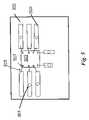
- FIG. 1depicts the exterior surfaces of a typical removable storage card package.
- This cardmay be of the type, for example, as described in U.S. Pat. No. 6,410,355 to Wallace, the inventor of the present application, which is incorporated herein by reference.
- a contact side of the cardfor example a secure digital or SD format card, is depicted with conductive terminals 101 arranged for contacting the integrated circuits within package 100 .
- FIG. 1 bdepicts the opposing side of the package 100 , which has no electrical contacts, but typically carries a label with information, brand name, size of media, and the like for the user's visual inspection and reference.
- the number of terminals, and the type of connections usedvaries with the format, for example for secure digital or SD, the terminals shown in FIG. 1 a are typical, and only a few external terminals are used.
- the terminals shown in FIG. 1 aare typical, and only a few external terminals are used.
- the terminalsare female receptacles located on one end of the side of the package.
- the camera or card readerhas a socket for receiving the same end of the CF package with male terminals or pins within the socket that enter the corresponding female receptacle when the compact flash card is inserted into the socket, thereby completing the connection.
- Other connectionsmay be used, for example a USB port may be used as the connection.
- the prior art packages for removable storage card devicestypically include a complex interposer or substrate in the form of a multiple layer laminate printed circuit board or “PC board”, which provides physical support and device-to-device connectivity for the controller integrated circuit and the memory device or devices.
- the boardwhich may be of BT resin, FR4, or fiberglass or similar, usually is a laminate structure that incorporates metal layers which are patterned to form conductor traces, vias coupling the various layers for making electrical connections, and lands for wire bonds to couple traces on the surface of the board to integrated circuit dies or other components, packaged or bare die components, which are mounted to the board.
- FIG. 2depicts a typical arrangement in a cross sectional view.
- a storage card 200 of the prior artis illustrated having integrated circuit dies 204 and 205 mounted on the same surface of laminated substrate 208 .
- Bond wires 203connect bond pads on the active surface, or face, of the integrated circuit dies to conductive areas, or lands 206 on the upper surface of the substrate.
- encapsulant 211which may be thermosetting or room temperature mold compounds or other encapsulating material.
- shell 201which may be plastic, covering the substrate and molded materials.
- Pat. No. 6,639,309 to Wallacedepicts a removable storage card incorporating a memory device and a controller device on opposing surfaces of a multilayer PC board material, with wire bonding connections, and an overmolding encapsulation.
- the integrated circuit dies and their respective leadframesare arranged in back-to-back relation and each die is coupled to the respective leadframe by the use of bond wires, or alternatively, the integrated circuits are arranged in a face-to-face relation on opposing sides of an interposer and coupled to their respective leadframe in a flip-chip arrangement, the two integrated circuits are independently coupled to external leads arranged on opposing sides of the packaged device and are not in electrical communication with each other.
- 6,316,825 to Park et al.also incorporated herein by reference, provides a stacked package for stacking two identical integrated circuit devices, such as memory devices, in a molded package with two leadframes, which are physically coupled at the exterior of the package, such that each signal coupled to the external leads is physically and electrically coupled to each of the two identical memory devices, which are connected in parallel fashion.
- Various preferred embodiments of the present inventionprovide a package for multiple semiconductor integrated circuits or dies, which connects two or more of the integrated circuits electrically, provides mechanical support for the integrated circuits, provides the facility to make arbitrary connections between the integrated circuits, and provides electrical connectivity to external connections of a packaged device.
- the packages of the inventiondo not require an interposer or substrate of type used in the prior art, and the materials use conventional wire bonding and leadframe technologies compatible with existing equipment and automated factory machines known in the semiconductor processing industry; such that no retooling or specialized equipment are required to use and implement the invention.
- a first leadframeis provided and positioned overlying a simple insulator layer.
- the insulator layerhas vias that are openings formed in certain locations and some leads of the leadframe overlie the vias. Other leads of the leadframe may extend to the external boundary of the insulator or beyond the edge of the insulator. Some leads of the leadframe may not be extended to the external connectors.
- a first integrated circuit dieis provided and positioned in proximity to the interior ends of the leadframes, in some embodiments the leadframe may have an opening provided in the interior and the die may be placed in the interior opening. In other embodiments, the die may rest over the leads of the leadframe, or under the leads of the leadframe.
- the dieis wire bonded to the leadframe to electrically connect one or more of the leads of the integrated circuit to the leads of the leadframe.
- the leads of the leadframemay be connected to the die using flip chip technology as is known in the art.
- a second leadframeis then placed overlying the second and opposing surface of the insulator.
- Certain leads of the second leadframeare positioned overlying the through-hole vias of the insulator as for, and in correspondence with, certain leads of the first leadframe.
- Other leads of the second leadframemay extend to the exterior of the insulator layer for making external electrical connections to the completed device, and may extend beyond the exterior boundary of the insulator.
- a second integrated circuit dieis placed in proximity to the interior leads of the second leadframe.
- the second leadframemay have a space in the central portion adjacent the interior ends of the leads of the leadframe for receiving the die, or a lead under chip or lead over chip leadframe arrangement may be used.
- certain leads of the first and second leadframeare electrically coupled through the vias in the insulator.
- This aspect of the inventionmakes it possible to electrically couple the first and second integrated circuit dies in an arbitrary location through the facility of making an electrical connection between the two leadframes through the insulator.
- the connectionmay be made by physically deforming the leadframe leads of the first and second leads into the space within the via in the insulator, and then making a physical contact between the two leads within the via.
- a conductive weldis then made between the two leadframes. The weld can be made, for example, with energy applied by heat, electrical energy, ultrasonic energy, laser energy, and the like.
- the electrical connectionsmay be made between the two leadframes by providing conductive materials positioned within the via, such as a conductive paste that acts as an electrical connection and which connection may be completed using thermal or electrical energy.
- the insulatormay be formed of an anisotropically conductive material that initially acts as an insulator in all directions, but becomes selectively conductive in a vertical direction when pressure or thermal energy or both is applied in an area, while remaining an insulator in the planar directions.
- a viais a region in which electrical conductivity is achieved between a conductor adjacent to the top surface of the insulator and a conductor adjacent to the bottom surface of the insulator.
- the inventionmay provide an insulator with vias formed in selected locations, a first leadframe overlying one surface of the insulator layer, a second leadframe overlying the opposing insulator layer, a first integrated circuit coupled to the first leadframe using known flip chip technology, where the integrated circuit bond pads are positioned in physical proximity to the desired leads and balls or pads of solder are formed, which are then reflowed using energy to form a mechanical and electrical connection between the die pads and the interior of the leads; the second integrated circuit may likewise be coupled to the second leadframe using flip chip technology, as before the completed device has electrical connections made between the first and second integrated circuits through the vias in the insulator. Since the first and second dies in this preferred embodiment are both coupled to the leadframe using flip chip technology, the integrated circuit devices may be arranged in face-to-face relation.
- a removable storage cardis formed using the packaging apparatus and methods of the invention; an insulator layer is provided with vias formed in selected locations, a first leadframe is positioned overlying the insulator and having some leads overlying the vias in the insulator, a first integrated circuit, which is a nonvolatile memory device, is positioned in proximity to the first leadframe and at least one electrical connection is made between the nonvolatile integrated circuit and the leadframe, a second integrated circuit is provided in proximity to a second leadframe, which is positioned overlying the opposing surface of the insulator and having some leads, which overlie the vias in the insulator, the second integrated circuit being a controller circuit for operating the nonvolatile memory device, the second integrated circuit is electrically connected to the second leadframe.
- the insulator used in the preferred embodiments of the present inventionmay comprise a variety of known materials. Because no electrical connections, complex multilayer routing, or metallization patterns are required within or on the insulator, the insulator may be formed of any material which electrically insulates the first and second leadframe one from another and which also may have through-hole vias formed within it. Plastic, glass, ceramic, fiberglass, resin, PC board, tapes, films, papers and other insulators may be used. Chemical etching, photolithography, laser drilling, or mechanical drilling processes may form the vias. Plastic or resin molding may be used to form an insulator with vias formed in it. The insulator can be formed in a wide variety of thicknesses and may be rigid or flexible material as desired.
- an integrated systemmay be provided in a single package by incorporating multiple integrated circuit dies on either side of an insulator, the multiple dies being wire bonded to leadframes, which are coupled through vias in the insulator to make arbitrary connections between the integrated circuits, wherein the packaged assembly for the system includes passive elements, such as resistors, capacitors, or inductors. The entire assembly can then be overmolded into a completed packaged system being provided using the methods of the invention.
- Advantages of embodiments of the present inventioninclude providing apparatus and methods of forming multiple integrated circuit modules including multiple integrated circuit devices which are electrically coupled to each other without the need for the complex interposers, flex circuits, laminate substrates or patterned printed circuit boards of the prior art, using conventional wire bonding or flip chip technologies and package molding methods, which are compatible with existing tooling, and using materials compatible with the existing automated semiconductor packaging infrastructure.
- FIG. 1depicts in a top view in FIG. 1 a and in a bottom view in FIG. 1 b a prior art removable storage card package;
- FIG. 2depicts a cross-sectional view of a prior art removable storage card such, as is illustrated in FIG. 1 , including a memory device and a controller device;
- FIG. 5depicts a top view of an insulator layer such as in FIGS. 3 , 4 and having a leadframe and an integrated circuit positioned on the insulator;
- FIG. 6depicts in a cross-sectional view the device of FIG. 5 , following additional processing steps;
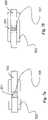
- FIGS. 7 a , 7 bdepict in a cross-section additional preferred embodiments of the insulator layer of the present invention.
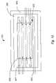
- FIG. 10depicts a top view of the device of FIG. 9 .
- the through-hole viascan be of any size but in a preferred embodiment are around 3-10 mils in diameter and preferably about 5 mils in diameter.
- the viasare open through-holes, in other embodiments described below the vias may be filled with conductive pastes, or adhesives.
- FIG. 4depicts the insulating layer of FIG. 3 in a cross-sectional view.
- the through-hole vias 301are shown extending through the insulating layer 300 .
- the through-hole vias 301may be formed by, for example, laser drilling, mechanical drilling, etching, punching or using other means to form holes in materials, such as molding.
- Photolithographymay be used to pattern an etch resistant layer over the surface with positive or negative resists used to define the locations and dimensions of the holes, selective etch may be applied to remove the material, and then the pattern layers may be stripped away, as is known in the art.
- FIG. 5depicts a top view of a preferred embodiment of the invention, after a number of assembly steps have been completed.
- the insulator layer 300has been provided with through-hole vias 301 formed in selected locations.
- a leadframeis provided with leads 502 and includes certain leads that overlie through-hole via locations 301 .
- Integrated circuit die 303is positioned in proximity to the interior ends of leads 502 .
- Bond wires 505are formed and electrically couple the bond pads 507 to the leads 502 .
- a symmetrical operationis performed to locate a second leadframe and a second integrated circuit die on the opposite surface of insulator layer 300 , with some leads of the second leadframe located under the through-hole vias 301 .
- a toolsuch as 607 in FIG. 6 is used to form the weld between the upper and lower leadframe leads and to simultaneously form the through-hole via 301 in the insulator layer 300 , that is, the insulator has no holes formed in it initially, the leadframes are positioned on either side opposing one another, and at locations where it is desired to couple the leads from the upper and lower leadframe together.
- welding tool 607is used to apply energy, such as heat, to the leads at a location where a connection is desired, the insulator material melts or vaporizes in response to the energy and a through-hole via 301 is formed as the insulator material is removed, the leads are physically deformed into the through-hole via 301 and are then welded together in a single continuous operation.
- energysuch as heat
- the conductive materialmay be a conductive paste screened into the vias as is known in the art, or a conductive ink, for example, a conductive ink material is available under the trade name Parmod VLT from Parelec of Rocky Hill, N.J.; and this material may be applied by screen printing, laser mill and filling, or ink jet printing processes. Heat or other energy may be applied to complete the conductive path and to physically bond the leads to the conductive material.
- 3M Tape 9703is an example product which may be used.
- Anisotropic films and conductive pastes for use in embodiments such as FIG. 7 b (film) or FIG. 7 a (paste)are also available from other commercial vendors, such as Henikel Technologies, of Dusseldorf, Germany. These materials may be used with other films or alone to provide the insulator layer 300 .
- Integrated circuit die 303which may be a memory controller device, is flip-chip bonded to the upper leadframe by first performing a well known die or wafer bumping process which forms solder bumps, balls or columns on the die pads of the integrated circuit, the solder bumped die is then aligned with the interior ends of the leadframe leads and positioned “face down” to couple the die pads to the leadframe leads, thermal energy is used to reflow the solder and complete the connection to the leadframe.
- integrated circuit 809which may be for example a nonvolatile memory, such as a FLASH memory device, is also flip-chip mounted to the lower leadframe, and welds, such as 807 , are formed to couple the upper and lower leadframes together in the through-hole vias 301 .
- FIG. 8also depicts the ability of the invention to make arbitrarily located connections between two or more integrated circuits within the package, the dies need not be identical or even nearly the same size.
- FIG. 10depicts the package 901 of FIG. 9 in a top view.
- Insulator layer 300is shown with encapsulant 903 formed on it.
- Leads 502are shown overlying insulator layer 300
- Welds 807are shown lying in vias formed underneath certain leads 502 .
- Integrated circuit die 303is positioned over the leads 502 , so that the leadframe is a LUC or lead under chip arrangement, the die may be attached by tape or epoxy to provide support. Bond pads on the integrated circuit are coupled to the leadframe leads 520 by bond wires 505 . Not visible in this view is the second integrated circuit and leadframe assembly lying underneath the insulator layer 300 and coupled to the upper leadframe by welds 807 .
- the leadframes and insulator layer 300may be assembled together as a pre-formed assembly and the integrated circuit dies positioned adjacent the corresponding leadframe, wire bonding or flip-chip coupling is used to complete the connection to the dies, and then overmolding or glop top encapsulation can be performed.
- the leadframesmay be provided in strip form, the integrated circuit dies may be positioned and wire bonding or flip-chip processing is performed to couple the integrated circuits to the leadframes with or without adhesives or tapes; the leadframe assemblies are then positioned over the respective opposing surfaces of the insulator layer 300 , the through-hole vias 301 already provided by patterning the insulator layer 300 ahead of time, and then the leadframes are coupled together by welding, use of conductive pastes or solders, or anisotropic conductor connection as described above. Finally, the completed assembly may be overmolded or glob top encapsulated, completing the package.
- the insulator layer 300as described above, may in another alternative method be provided without through-hole vias 301 formed within it, and the tooling may be used to weld and simultaneously form the through-hole vias 301 in the insulator layer 300 .
Landscapes
- Physics & Mathematics (AREA)
- Condensed Matter Physics & Semiconductors (AREA)
- General Physics & Mathematics (AREA)
- Engineering & Computer Science (AREA)
- Computer Hardware Design (AREA)
- Microelectronics & Electronic Packaging (AREA)
- Power Engineering (AREA)
- Lead Frames For Integrated Circuits (AREA)
- Structures Or Materials For Encapsulating Or Coating Semiconductor Devices Or Solid State Devices (AREA)
Abstract
Description
Claims (17)
Priority Applications (9)
| Application Number | Priority Date | Filing Date | Title |
|---|---|---|---|
| US11/264,112US7511371B2 (en) | 2005-11-01 | 2005-11-01 | Multiple die integrated circuit package |
| EP06827158AEP1949440A2 (en) | 2005-11-01 | 2006-10-30 | Multiple die integrated circuit package |
| KR1020087013254AKR100996982B1 (en) | 2005-11-01 | 2006-10-30 | Multi Die Integrated Circuit Package |
| PCT/US2006/042450WO2007053606A2 (en) | 2005-11-01 | 2006-10-30 | Multiple die integrated circuit package |
| CN2006800450011ACN101341593B (en) | 2005-11-01 | 2006-10-30 | Multiple die integrated circuit package |
| TW095140244ATWI324385B (en) | 2005-11-01 | 2006-10-31 | Multiple die integrated circuit package |
| TW098135181ATWI475662B (en) | 2005-11-01 | 2006-10-31 | Multiple die integrated circuit package |
| US12/203,496US7939920B2 (en) | 2005-11-01 | 2008-09-03 | Multiple die integrated circuit package |
| US12/430,388US8030135B2 (en) | 2005-11-01 | 2009-04-27 | Methods for a multiple die integrated circuit package |
Applications Claiming Priority (1)
| Application Number | Priority Date | Filing Date | Title |
|---|---|---|---|
| US11/264,112US7511371B2 (en) | 2005-11-01 | 2005-11-01 | Multiple die integrated circuit package |
Related Child Applications (1)
| Application Number | Title | Priority Date | Filing Date |
|---|---|---|---|
| US12/203,496DivisionUS7939920B2 (en) | 2005-11-01 | 2008-09-03 | Multiple die integrated circuit package |
Publications (2)
| Publication Number | Publication Date |
|---|---|
| US20070096265A1 US20070096265A1 (en) | 2007-05-03 |
| US7511371B2true US7511371B2 (en) | 2009-03-31 |
Family
ID=37995166
Family Applications (3)
| Application Number | Title | Priority Date | Filing Date |
|---|---|---|---|
| US11/264,112Active2026-05-14US7511371B2 (en) | 2005-11-01 | 2005-11-01 | Multiple die integrated circuit package |
| US12/203,496Active2026-09-06US7939920B2 (en) | 2005-11-01 | 2008-09-03 | Multiple die integrated circuit package |
| US12/430,388Expired - Fee RelatedUS8030135B2 (en) | 2005-11-01 | 2009-04-27 | Methods for a multiple die integrated circuit package |
Family Applications After (2)
| Application Number | Title | Priority Date | Filing Date |
|---|---|---|---|
| US12/203,496Active2026-09-06US7939920B2 (en) | 2005-11-01 | 2008-09-03 | Multiple die integrated circuit package |
| US12/430,388Expired - Fee RelatedUS8030135B2 (en) | 2005-11-01 | 2009-04-27 | Methods for a multiple die integrated circuit package |
Country Status (2)
| Country | Link |
|---|---|
| US (3) | US7511371B2 (en) |
| CN (1) | CN101341593B (en) |
Cited By (13)
| Publication number | Priority date | Publication date | Assignee | Title |
|---|---|---|---|---|
| US20070130759A1 (en)* | 2005-06-15 | 2007-06-14 | Gem Services, Inc. | Semiconductor device package leadframe formed from multiple metal layers |
| US20080150102A1 (en)* | 2006-10-16 | 2008-06-26 | Fuji Electric Device Technology Co., Ltd. | Semiconductor device and manufacturing method of semiconductor device |
| US20080179722A1 (en)* | 2007-01-31 | 2008-07-31 | Cyntec Co., Ltd. | Electronic package structure |
| US20080303130A1 (en)* | 2007-06-11 | 2008-12-11 | Chin-Ti Chen | Package on package structure |
| US20090039491A1 (en)* | 2007-08-10 | 2009-02-12 | Samsung Electronics Co., Ltd. | Semiconductor package having buried post in encapsulant and method of manufacturing the same |
| US20090239340A1 (en)* | 2005-11-01 | 2009-09-24 | Wallace Robert F | Methods for a multiple die integrated circuit package |
| US9122968B2 (en) | 2012-04-03 | 2015-09-01 | X-Card Holdings, Llc | Information carrying card comprising a cross-linked polymer composition, and method of making the same |
| US9439334B2 (en) | 2012-04-03 | 2016-09-06 | X-Card Holdings, Llc | Information carrying card comprising crosslinked polymer composition, and method of making the same |
| US20160260691A1 (en)* | 2013-10-07 | 2016-09-08 | Toyota Jidosha Kabushiki Kaisha | Semiconductor module |
| US20190088571A1 (en)* | 2012-01-05 | 2019-03-21 | Ixys, Llc | Discrete power transistor package having solderless dbc to leadframe attach |
| US10906287B2 (en) | 2013-03-15 | 2021-02-02 | X-Card Holdings, Llc | Methods of making a core layer for an information carrying card, and resulting products |
| US11361204B2 (en) | 2018-03-07 | 2022-06-14 | X-Card Holdings, Llc | Metal card |
| US12220897B2 (en) | 2022-10-20 | 2025-02-11 | X-Card Holdings, Llc | Core layer for information carrying card, resulting information carrying card, and methods of making the same |
Families Citing this family (24)
| Publication number | Priority date | Publication date | Assignee | Title |
|---|---|---|---|---|
| US7352058B2 (en)* | 2005-11-01 | 2008-04-01 | Sandisk Corporation | Methods for a multiple die integrated circuit package |
| US7408243B2 (en)* | 2005-12-14 | 2008-08-05 | Honeywell International Inc. | High temperature package flip-chip bonding to ceramic |
| KR100770690B1 (en)* | 2006-03-15 | 2007-10-29 | 삼성전기주식회사 | Camera Module Package |
| US20080180921A1 (en)* | 2007-01-31 | 2008-07-31 | Cyntec Co., Ltd. | Electronic package structure |
| WO2008131058A2 (en)* | 2007-04-17 | 2008-10-30 | Rambus Inc. | Hybrid volatile and non-volatile memory device |
| US8141786B2 (en)* | 2008-01-18 | 2012-03-27 | Texas Instruments Incorporated | Thin smart card module having strap on carrier |
| US7868433B2 (en)* | 2008-08-29 | 2011-01-11 | National Semiconductor Corporation | Low stress cavity package |
| US8115286B2 (en)* | 2008-10-22 | 2012-02-14 | Honeywell International Inc. | Integrated sensor including sensing and processing die mounted on opposite sides of package substrate |
| US8093695B2 (en)* | 2009-09-04 | 2012-01-10 | International Rectifier Corporation | Direct contact leadless flip chip package for high current devices |
| JP2011060927A (en)* | 2009-09-09 | 2011-03-24 | Hitachi Ltd | Semiconductor apparatus |
| US8212342B2 (en) | 2009-12-10 | 2012-07-03 | Stats Chippac Ltd. | Integrated circuit package system with removable backing element having plated terminal leads and method of manufacture thereof |
| US8502372B2 (en) | 2010-08-26 | 2013-08-06 | Lsi Corporation | Low-cost 3D face-to-face out assembly |
| US8264074B2 (en)* | 2010-09-10 | 2012-09-11 | General Electric Company | Device for use as dual-sided sensor package |
| JP2013025540A (en)* | 2011-07-20 | 2013-02-04 | Toshiba Corp | Semiconductor storage device |
| US8525312B2 (en)* | 2011-08-12 | 2013-09-03 | Tessera, Inc. | Area array quad flat no-lead (QFN) package |
| CN103268875B (en)* | 2013-05-30 | 2015-06-03 | 山东华芯微电子科技有限公司 | Multi-wafer encapsulating structure |
| US9480161B2 (en) | 2014-01-17 | 2016-10-25 | Freescale Semiconductor, Inc. | Thin low profile strip dual in-line memory module |
| TWI550823B (en)* | 2014-04-10 | 2016-09-21 | 南茂科技股份有限公司 | Chip package structure |
| US10002653B2 (en) | 2014-10-28 | 2018-06-19 | Nxp Usa, Inc. | Die stack address bus having a programmable width |
| US10418343B2 (en)* | 2017-12-05 | 2019-09-17 | Infineon Technologies Ag | Package-in-package structure for semiconductor devices and methods of manufacture |
| JP7271337B2 (en) | 2019-06-27 | 2023-05-11 | 新光電気工業株式会社 | Electronic component device and method for manufacturing electronic component device |
| JP2022146312A (en) | 2021-03-22 | 2022-10-05 | キオクシア株式会社 | Semiconductor device |
| CN115636131B (en)* | 2022-10-25 | 2024-11-26 | 苏州浪潮智能科技有限公司 | A system, method, device and medium for realizing automatic absorption of server components |
| US20240429137A1 (en)* | 2023-06-20 | 2024-12-26 | Nxp B.V. | Dual leadframe semiconductor device and method therefor |
Citations (40)
| Publication number | Priority date | Publication date | Assignee | Title |
|---|---|---|---|---|
| US4288841A (en) | 1979-09-20 | 1981-09-08 | Bell Telephone Laboratories, Incorporated | Double cavity semiconductor chip carrier |
| JPS5763850A (en) | 1980-10-06 | 1982-04-17 | Nec Corp | Semiconductor device |
| US4423468A (en) | 1980-10-01 | 1983-12-27 | Motorola, Inc. | Dual electronic component assembly |
| JPH0330494A (en) | 1989-06-28 | 1991-02-08 | Sharp Corp | Method for forming through-hole portions of flexible circuit boards |
| US5147815A (en) | 1990-05-14 | 1992-09-15 | Motorola, Inc. | Method for fabricating a multichip semiconductor device having two interdigitated leadframes |
| US5220195A (en) | 1991-12-19 | 1993-06-15 | Motorola, Inc. | Semiconductor device having a multilayer leadframe with full power and ground planes |
| US5239198A (en)* | 1989-09-06 | 1993-08-24 | Motorola, Inc. | Overmolded semiconductor device having solder ball and edge lead connective structure |
| WO1993026144A1 (en) | 1992-06-15 | 1993-12-23 | Dyconex Patente Ag | Process for producing subsequently conditionable contact points on circuit substrates and circuit substrates with such contact points |
| DE19522338A1 (en) | 1995-06-20 | 1997-01-02 | Fraunhofer Ges Forschung | Deformable substrate through-contact production method for chip carrier |
| EP0798772A1 (en) | 1996-03-26 | 1997-10-01 | Commissariat A L'energie Atomique | Process for realizing a deposition on a detachable support, and realized deposition on a support |
| DE19648492A1 (en) | 1996-11-22 | 1997-11-13 | Siemens Ag | Three=dimensional multi-chip module, e.g. memory module |
| US5715193A (en)* | 1996-05-23 | 1998-02-03 | Micron Quantum Devices, Inc. | Flash memory system and method for monitoring the disturb effect on memory cell blocks due to high voltage conditions of other memory cell blocks |
| US5798564A (en)* | 1995-12-21 | 1998-08-25 | Texas Instruments Incorporated | Multiple chip module apparatus having dual sided substrate |
| US5801072A (en)* | 1996-03-14 | 1998-09-01 | Lsi Logic Corporation | Method of packaging integrated circuits |
| US5861668A (en)* | 1996-06-14 | 1999-01-19 | Lg Semicon Co., Ltd. | Semiconductor package |
| USRE36077E (en)* | 1991-10-15 | 1999-02-02 | Mitsubishi Denki Kabushiki Kaisha | Method of manufacturing inversion type IC's and IC module using same |
| US5880403A (en)* | 1994-04-01 | 1999-03-09 | Space Electronics, Inc. | Radiation shielding of three dimensional multi-chip modules |
| US6051878A (en)* | 1997-03-10 | 2000-04-18 | Micron Technology, Inc. | Method of constructing stacked packages |
| US6069025A (en)* | 1994-11-15 | 2000-05-30 | Lg Semicon Co., Ltd. | Method for packaging a semiconductor device |
| US6079987A (en)* | 1997-12-26 | 2000-06-27 | Unitechno, Inc. | Connector for electronic parts |
| US6153928A (en)* | 1996-05-17 | 2000-11-28 | Hyuandai Electronics Industries Co., Ltd. | Substrate for semiconductor package, fabrication method thereof, and stacked-type semiconductor package using the substrate |
| US6239496B1 (en) | 1999-01-18 | 2001-05-29 | Kabushiki Kaisha Toshiba | Package having very thin semiconductor chip, multichip module assembled by the package, and method for manufacturing the same |
| US6291892B1 (en)* | 1998-04-02 | 2001-09-18 | Oki Electric Industry Co., Ltd | Semiconductor package that includes a shallow metal basin surrounded by an insulator frame |
| US6313598B1 (en)* | 1998-09-11 | 2001-11-06 | Hitachi, Ltd. | Power semiconductor module and motor drive system |
| US6316825B1 (en) | 1998-05-15 | 2001-11-13 | Hyundai Electronics Industries Co., Ltd. | Chip stack package utilizing a connecting hole to improve electrical connection between leadframes |
| US6410355B1 (en) | 1998-06-11 | 2002-06-25 | Sandisk Corporation | Semiconductor package using terminals formed on a conductive layer of a circuit board |
| US20020084522A1 (en) | 2000-10-10 | 2002-07-04 | Akira Yoshizawa | Semiconductor device using interposer substrate and manufacturing method therefor |
| US20020121690A1 (en) | 1987-06-24 | 2002-09-05 | Hitachi, Ltd. (Jp) | Semiconductor memory module having double-sided stacked memory chip layout |
| US6448636B2 (en) | 1999-03-09 | 2002-09-10 | Rohm Co., Ltd. | Multi-layered integrated semiconductor device incorporating electrically connected integrated circuit chips and monitoring pads |
| US6472732B1 (en)* | 1999-10-25 | 2002-10-29 | Oki Electric Industry Co., Ltd. | BGA package and method for fabricating the same |
| US6521483B1 (en)* | 1999-07-22 | 2003-02-18 | Seiko Epson Corporation | Semiconductor device, method of manufacture thereof, circuit board, and electronic device |
| US6603197B1 (en) | 2002-06-12 | 2003-08-05 | Mitsubishi Denki Kabushiki Kaisha | Semiconductor unit |
| US6639309B2 (en) | 2002-03-28 | 2003-10-28 | Sandisk Corporation | Memory package with a controller on one side of a printed circuit board and memory on another side of the circuit board |
| US20040089717A1 (en) | 2002-11-13 | 2004-05-13 | Sandisk Corporation | Universal non-volatile memory card used with various different standard cards containing a memory controller |
| US6753207B2 (en)* | 2000-01-04 | 2004-06-22 | Hyundai Electronics Industries Co., Ltd. | Stacked semiconductor package and fabricating method thereof |
| US6774473B1 (en)* | 1999-07-30 | 2004-08-10 | Ming-Tung Shen | Semiconductor chip module |
| US20040169285A1 (en) | 2002-02-19 | 2004-09-02 | Vani Verma | Memory module having interconnected and stacked integrated circuits |
| US6815251B1 (en)* | 1999-02-01 | 2004-11-09 | Micron Technology, Inc. | High density modularity for IC's |
| US6872903B2 (en)* | 2002-12-16 | 2005-03-29 | Agilent Technologies, Inc. | Surface joined multi-substrate liquid metal switching device |
| US20060102995A1 (en) | 2004-11-12 | 2006-05-18 | Tsai Chen J | Apparatus for stacking electrical components using insulated and interconnecting via |
Family Cites Families (10)
| Publication number | Priority date | Publication date | Assignee | Title |
|---|---|---|---|---|
| US5438224A (en)* | 1992-04-23 | 1995-08-01 | Motorola, Inc. | Integrated circuit package having a face-to-face IC chip arrangement |
| KR100192179B1 (en)* | 1996-03-06 | 1999-06-15 | 김영환 | Semiconductor package |
| US6137164A (en)* | 1998-03-16 | 2000-10-24 | Texas Instruments Incorporated | Thin stacked integrated circuit device |
| TW561266B (en)* | 1999-09-17 | 2003-11-11 | Jsr Corp | Anisotropic conductive sheet, its manufacturing method, and connector |
| US6462421B1 (en)* | 2000-04-10 | 2002-10-08 | Advanced Semicondcutor Engineering, Inc. | Multichip module |
| KR100415281B1 (en)* | 2001-06-29 | 2004-01-16 | 삼성전자주식회사 | Double-side Mounting Circuit Board and Multi Chip Package including the Such a Circuit Board |
| SG114585A1 (en)* | 2002-11-22 | 2005-09-28 | Micron Technology Inc | Packaged microelectronic component assemblies |
| JP3797992B2 (en)* | 2003-09-05 | 2006-07-19 | 沖電気工業株式会社 | Semiconductor device |
| US7511371B2 (en)* | 2005-11-01 | 2009-03-31 | Sandisk Corporation | Multiple die integrated circuit package |
| US7352058B2 (en)* | 2005-11-01 | 2008-04-01 | Sandisk Corporation | Methods for a multiple die integrated circuit package |
- 2005
- 2005-11-01USUS11/264,112patent/US7511371B2/enactiveActive
- 2006
- 2006-10-30CNCN2006800450011Apatent/CN101341593B/ennot_activeExpired - Fee Related
- 2008
- 2008-09-03USUS12/203,496patent/US7939920B2/enactiveActive
- 2009
- 2009-04-27USUS12/430,388patent/US8030135B2/ennot_activeExpired - Fee Related
Patent Citations (42)
| Publication number | Priority date | Publication date | Assignee | Title |
|---|---|---|---|---|
| US4288841A (en) | 1979-09-20 | 1981-09-08 | Bell Telephone Laboratories, Incorporated | Double cavity semiconductor chip carrier |
| US4423468A (en) | 1980-10-01 | 1983-12-27 | Motorola, Inc. | Dual electronic component assembly |
| JPS5763850A (en) | 1980-10-06 | 1982-04-17 | Nec Corp | Semiconductor device |
| US20020121690A1 (en) | 1987-06-24 | 2002-09-05 | Hitachi, Ltd. (Jp) | Semiconductor memory module having double-sided stacked memory chip layout |
| US6693346B2 (en) | 1987-06-24 | 2004-02-17 | Hitachi, Ltd. | Semiconductor memory module having double-sided stacked memory chip layout |
| JPH0330494A (en) | 1989-06-28 | 1991-02-08 | Sharp Corp | Method for forming through-hole portions of flexible circuit boards |
| US5239198A (en)* | 1989-09-06 | 1993-08-24 | Motorola, Inc. | Overmolded semiconductor device having solder ball and edge lead connective structure |
| US5147815A (en) | 1990-05-14 | 1992-09-15 | Motorola, Inc. | Method for fabricating a multichip semiconductor device having two interdigitated leadframes |
| USRE36077E (en)* | 1991-10-15 | 1999-02-02 | Mitsubishi Denki Kabushiki Kaisha | Method of manufacturing inversion type IC's and IC module using same |
| US5220195A (en) | 1991-12-19 | 1993-06-15 | Motorola, Inc. | Semiconductor device having a multilayer leadframe with full power and ground planes |
| WO1993026144A1 (en) | 1992-06-15 | 1993-12-23 | Dyconex Patente Ag | Process for producing subsequently conditionable contact points on circuit substrates and circuit substrates with such contact points |
| US5880403A (en)* | 1994-04-01 | 1999-03-09 | Space Electronics, Inc. | Radiation shielding of three dimensional multi-chip modules |
| US6069025A (en)* | 1994-11-15 | 2000-05-30 | Lg Semicon Co., Ltd. | Method for packaging a semiconductor device |
| DE19522338A1 (en) | 1995-06-20 | 1997-01-02 | Fraunhofer Ges Forschung | Deformable substrate through-contact production method for chip carrier |
| US5798564A (en)* | 1995-12-21 | 1998-08-25 | Texas Instruments Incorporated | Multiple chip module apparatus having dual sided substrate |
| US5801072A (en)* | 1996-03-14 | 1998-09-01 | Lsi Logic Corporation | Method of packaging integrated circuits |
| EP0798772A1 (en) | 1996-03-26 | 1997-10-01 | Commissariat A L'energie Atomique | Process for realizing a deposition on a detachable support, and realized deposition on a support |
| US6153928A (en)* | 1996-05-17 | 2000-11-28 | Hyuandai Electronics Industries Co., Ltd. | Substrate for semiconductor package, fabrication method thereof, and stacked-type semiconductor package using the substrate |
| US5715193A (en)* | 1996-05-23 | 1998-02-03 | Micron Quantum Devices, Inc. | Flash memory system and method for monitoring the disturb effect on memory cell blocks due to high voltage conditions of other memory cell blocks |
| US5861668A (en)* | 1996-06-14 | 1999-01-19 | Lg Semicon Co., Ltd. | Semiconductor package |
| DE19648492A1 (en) | 1996-11-22 | 1997-11-13 | Siemens Ag | Three=dimensional multi-chip module, e.g. memory module |
| US6051878A (en)* | 1997-03-10 | 2000-04-18 | Micron Technology, Inc. | Method of constructing stacked packages |
| US6079987A (en)* | 1997-12-26 | 2000-06-27 | Unitechno, Inc. | Connector for electronic parts |
| US6413798B2 (en)* | 1998-01-18 | 2002-07-02 | Kabushiki Kaisha Toshiba | Package having very thin semiconductor chip, multichip module assembled by the package, and method for manufacturing the same |
| US6291892B1 (en)* | 1998-04-02 | 2001-09-18 | Oki Electric Industry Co., Ltd | Semiconductor package that includes a shallow metal basin surrounded by an insulator frame |
| US6316825B1 (en) | 1998-05-15 | 2001-11-13 | Hyundai Electronics Industries Co., Ltd. | Chip stack package utilizing a connecting hole to improve electrical connection between leadframes |
| US6410355B1 (en) | 1998-06-11 | 2002-06-25 | Sandisk Corporation | Semiconductor package using terminals formed on a conductive layer of a circuit board |
| US6313598B1 (en)* | 1998-09-11 | 2001-11-06 | Hitachi, Ltd. | Power semiconductor module and motor drive system |
| US6239496B1 (en) | 1999-01-18 | 2001-05-29 | Kabushiki Kaisha Toshiba | Package having very thin semiconductor chip, multichip module assembled by the package, and method for manufacturing the same |
| US6815251B1 (en)* | 1999-02-01 | 2004-11-09 | Micron Technology, Inc. | High density modularity for IC's |
| US6448636B2 (en) | 1999-03-09 | 2002-09-10 | Rohm Co., Ltd. | Multi-layered integrated semiconductor device incorporating electrically connected integrated circuit chips and monitoring pads |
| US6521483B1 (en)* | 1999-07-22 | 2003-02-18 | Seiko Epson Corporation | Semiconductor device, method of manufacture thereof, circuit board, and electronic device |
| US6774473B1 (en)* | 1999-07-30 | 2004-08-10 | Ming-Tung Shen | Semiconductor chip module |
| US6472732B1 (en)* | 1999-10-25 | 2002-10-29 | Oki Electric Industry Co., Ltd. | BGA package and method for fabricating the same |
| US6753207B2 (en)* | 2000-01-04 | 2004-06-22 | Hyundai Electronics Industries Co., Ltd. | Stacked semiconductor package and fabricating method thereof |
| US20020084522A1 (en) | 2000-10-10 | 2002-07-04 | Akira Yoshizawa | Semiconductor device using interposer substrate and manufacturing method therefor |
| US20040169285A1 (en) | 2002-02-19 | 2004-09-02 | Vani Verma | Memory module having interconnected and stacked integrated circuits |
| US6639309B2 (en) | 2002-03-28 | 2003-10-28 | Sandisk Corporation | Memory package with a controller on one side of a printed circuit board and memory on another side of the circuit board |
| US6603197B1 (en) | 2002-06-12 | 2003-08-05 | Mitsubishi Denki Kabushiki Kaisha | Semiconductor unit |
| US20040089717A1 (en) | 2002-11-13 | 2004-05-13 | Sandisk Corporation | Universal non-volatile memory card used with various different standard cards containing a memory controller |
| US6872903B2 (en)* | 2002-12-16 | 2005-03-29 | Agilent Technologies, Inc. | Surface joined multi-substrate liquid metal switching device |
| US20060102995A1 (en) | 2004-11-12 | 2006-05-18 | Tsai Chen J | Apparatus for stacking electrical components using insulated and interconnecting via |
Non-Patent Citations (7)
| Title |
|---|
| "FCBGA (Flip Chip Ball Grid Array)", 1995 NEC Electronics Corporation, Feb. 6, 2007 http://www.necel.com/pkg/en/pk02-03.html. |
| International Search Report dated Jul. 9, 2007 in PCT Application No. PCT/US2006/042450. |
| Notice of Allowance dated Nov. 9, 2007, U.S. Appl. No. 11/264,556. |
| Office Action dated Apr. 10, 2007, U.S. Appl. No. 11/264,556, filed Nov. 1, 2005. |
| Office Action dated Oct. 16, 2007, U.S. Appl. No. 11/264,556, filed Nov. 1, 2005. |
| Response to Office Action dated Oct. 31, 2007, U.S. Appl. No. 11/264,556, filed Nov. 1, 2005. |
| U.S. Appl. No. 11/931,092, filed Oct. 31, 2007. |
Cited By (38)
| Publication number | Priority date | Publication date | Assignee | Title |
|---|---|---|---|---|
| US20070130759A1 (en)* | 2005-06-15 | 2007-06-14 | Gem Services, Inc. | Semiconductor device package leadframe formed from multiple metal layers |
| US20090239340A1 (en)* | 2005-11-01 | 2009-09-24 | Wallace Robert F | Methods for a multiple die integrated circuit package |
| US8030135B2 (en)* | 2005-11-01 | 2011-10-04 | Sandisk Technologies Inc. | Methods for a multiple die integrated circuit package |
| US20080150102A1 (en)* | 2006-10-16 | 2008-06-26 | Fuji Electric Device Technology Co., Ltd. | Semiconductor device and manufacturing method of semiconductor device |
| US7705443B2 (en)* | 2006-10-16 | 2010-04-27 | Fuji Electric Device Technology Co., Ltd. | Semiconductor device with lead frame including conductor plates arranged three-dimensionally |
| US20080179722A1 (en)* | 2007-01-31 | 2008-07-31 | Cyntec Co., Ltd. | Electronic package structure |
| US20080303130A1 (en)* | 2007-06-11 | 2008-12-11 | Chin-Ti Chen | Package on package structure |
| US20090039491A1 (en)* | 2007-08-10 | 2009-02-12 | Samsung Electronics Co., Ltd. | Semiconductor package having buried post in encapsulant and method of manufacturing the same |
| US8093703B2 (en)* | 2007-08-10 | 2012-01-10 | Samsung Electronics Co., Ltd. | Semiconductor package having buried post in encapsulant and method of manufacturing the same |
| US8846446B2 (en) | 2007-08-10 | 2014-09-30 | Samsung Electronics Co., Ltd. | Semiconductor package having buried post in encapsulant and method of manufacturing the same |
| US20190088571A1 (en)* | 2012-01-05 | 2019-03-21 | Ixys, Llc | Discrete power transistor package having solderless dbc to leadframe attach |
| US10720376B2 (en)* | 2012-01-05 | 2020-07-21 | Littelfuse, Inc. | Discrete power transistor package having solderless DBC to leadframe attach |
| US11387162B2 (en) | 2012-01-05 | 2022-07-12 | Littelfuse, Inc. | Discrete power transistor package having solderless DBC to leadframe attach |
| US10127489B2 (en) | 2012-04-03 | 2018-11-13 | X-Card Holdings, Llc | Information carrying card comprising crosslinked polymer composition, and method of making the same |
| US11555108B2 (en) | 2012-04-03 | 2023-01-17 | Idemia America Corp. | Information carrying card comprising a cross-linked polymer composition, and method of making the same |
| US9594999B2 (en) | 2012-04-03 | 2017-03-14 | X-Card Holdings, Llc | Information carrying card comprising crosslinked polymer composition, and method of making the same |
| US9688850B2 (en) | 2012-04-03 | 2017-06-27 | X-Card Holdings, Llc | Information carrying card comprising a cross-linked polymer composition, and method of making the same |
| US9183486B2 (en) | 2012-04-03 | 2015-11-10 | X-Card Holdings, Llc | Information carrying card comprising a cross-linked polymer composition, and method of making the same |
| US9122968B2 (en) | 2012-04-03 | 2015-09-01 | X-Card Holdings, Llc | Information carrying card comprising a cross-linked polymer composition, and method of making the same |
| US10255539B2 (en) | 2012-04-03 | 2019-04-09 | X-Card Holdings, Llc | Information carrying card comprising crosslinked polymer composition, and method of making the same |
| US10392502B2 (en) | 2012-04-03 | 2019-08-27 | X-Card Holdings, Llc | Information carrying card comprising a cross-linked polymer composition, and method of making the same |
| US10570281B2 (en) | 2012-04-03 | 2020-02-25 | X-Card Holdings, Llc. | Information carrying card comprising a cross-linked polymer composition, and method of making the same |
| US10611907B2 (en) | 2012-04-03 | 2020-04-07 | X-Card Holdings, Llc | Information carrying card comprising a cross-linked polymer composition, and method of making the same |
| US9439334B2 (en) | 2012-04-03 | 2016-09-06 | X-Card Holdings, Llc | Information carrying card comprising crosslinked polymer composition, and method of making the same |
| US10836894B2 (en) | 2012-04-03 | 2020-11-17 | X-Card Holdings, Llc | Information carrying card comprising a cross-linked polymer composition, and method of making the same |
| US11170281B2 (en) | 2012-04-03 | 2021-11-09 | Idemia America Corp. | Information carrying card comprising crosslinked polymer composition, and method of making the same |
| US11560474B2 (en) | 2012-04-03 | 2023-01-24 | X-Card Holdings, Llc | Information carrying card comprising a cross-linked polymer composition, and method of making the same |
| US11359084B2 (en) | 2012-04-03 | 2022-06-14 | X-Card Holdings, Llc | Information carrying card comprising a cross-linked polymer composition, and method of making the same |
| US11359085B2 (en) | 2012-04-03 | 2022-06-14 | X-Card Holdings, Llc | Information carrying card comprising a cross-linked polymer composition, and method of making the same |
| US11390737B2 (en) | 2012-04-03 | 2022-07-19 | X-Card Holdings, Llc | Method of making an information carrying card comprising a cross-linked polymer composition |
| US9275321B2 (en) | 2012-04-03 | 2016-03-01 | X-Card Holdings, Llc | Information carrying card comprising a cross-linked polymer composition, and method of making the same |
| US10906287B2 (en) | 2013-03-15 | 2021-02-02 | X-Card Holdings, Llc | Methods of making a core layer for an information carrying card, and resulting products |
| US11884051B2 (en) | 2013-03-15 | 2024-01-30 | X-Card Holdings, Llc | Methods of making a core layer for an information carrying card, and resulting products |
| US20160260691A1 (en)* | 2013-10-07 | 2016-09-08 | Toyota Jidosha Kabushiki Kaisha | Semiconductor module |
| US11361204B2 (en) | 2018-03-07 | 2022-06-14 | X-Card Holdings, Llc | Metal card |
| US11853824B2 (en) | 2018-03-07 | 2023-12-26 | X-Card Holdings, Llc | Metal card |
| US12204966B2 (en) | 2018-03-07 | 2025-01-21 | X-Card Holdings, Llc | Metal card |
| US12220897B2 (en) | 2022-10-20 | 2025-02-11 | X-Card Holdings, Llc | Core layer for information carrying card, resulting information carrying card, and methods of making the same |
Also Published As
| Publication number | Publication date |
|---|---|
| US20080315382A1 (en) | 2008-12-25 |
| US20090239340A1 (en) | 2009-09-24 |
| US8030135B2 (en) | 2011-10-04 |
| CN101341593A (en) | 2009-01-07 |
| CN101341593B (en) | 2012-08-22 |
| US20070096265A1 (en) | 2007-05-03 |
| US7939920B2 (en) | 2011-05-10 |
Similar Documents
| Publication | Publication Date | Title |
|---|---|---|
| US7939920B2 (en) | Multiple die integrated circuit package | |
| US7514297B2 (en) | Methods for a multiple die integrated circuit package | |
| US7772686B2 (en) | Memory card fabricated using SiP/SMT hybrid technology | |
| US6441476B1 (en) | Flexible tape carrier with external terminals formed on interposers | |
| US9230942B2 (en) | Semiconductor device including alternating stepped semiconductor die stacks | |
| JP6027966B2 (en) | Stackable mold microelectronic package with area array unit connector | |
| JP5341337B2 (en) | Semiconductor device and manufacturing method thereof | |
| US8653653B2 (en) | High density three dimensional semiconductor die package | |
| US7829990B1 (en) | Stackable semiconductor package including laminate interposer | |
| US8728864B2 (en) | Method of fabricating a memory card using SIP/SMT hybrid technology | |
| US8729710B1 (en) | Semiconductor package with patterning layer and method of making same | |
| KR20090091114A (en) | How to Form a Single Layer Substrate for High Capacity Memory Cards | |
| KR100996982B1 (en) | Multi Die Integrated Circuit Package | |
| JP3781998B2 (en) | Manufacturing method of stacked semiconductor device | |
| KR20080051658A (en) | Printed circuit board and its manufacturing method, semiconductor package having said printed circuit board and manufacturing method | |
| US20080179721A1 (en) | Stacking of transfer carriers with aperture arrays as interconnection joints | |
| CN117393534A (en) | Chip packaging structure and electronic equipment |
Legal Events
| Date | Code | Title | Description |
|---|---|---|---|
| AS | Assignment | Owner name:SANDISK CORPORATION, CALIFORNIA Free format text:ASSIGNMENT OF ASSIGNORS INTEREST;ASSIGNOR:WALLACE, BOB;REEL/FRAME:017632/0223 Effective date:20051025 | |
| STCF | Information on status: patent grant | Free format text:PATENTED CASE | |
| CC | Certificate of correction | ||
| AS | Assignment | Owner name:SANDISK TECHNOLOGIES INC., TEXAS Free format text:ASSIGNMENT OF ASSIGNORS INTEREST;ASSIGNOR:SANDISK CORPORATION;REEL/FRAME:026349/0396 Effective date:20110404 | |
| FPAY | Fee payment | Year of fee payment:4 | |
| AS | Assignment | Owner name:SANDISK TECHNOLOGIES LLC, TEXAS Free format text:CHANGE OF NAME;ASSIGNOR:SANDISK TECHNOLOGIES INC;REEL/FRAME:038809/0472 Effective date:20160516 | |
| FPAY | Fee payment | Year of fee payment:8 | |
| MAFP | Maintenance fee payment | Free format text:PAYMENT OF MAINTENANCE FEE, 12TH YEAR, LARGE ENTITY (ORIGINAL EVENT CODE: M1553); ENTITY STATUS OF PATENT OWNER: LARGE ENTITY Year of fee payment:12 | |
| AS | Assignment | Owner name:SANDISK TECHNOLOGIES, INC., CALIFORNIA Free format text:ASSIGNMENT OF ASSIGNORS INTEREST;ASSIGNOR:SANDISK TECHNOLOGIES LLC;REEL/FRAME:069796/0423 Effective date:20241227 | |
| AS | Assignment | Owner name:SANDISK TECHNOLOGIES, INC., CALIFORNIA Free format text:PARTIAL RELEASE OF SECURITY INTERESTS;ASSIGNOR:JPMORGAN CHASE BANK, N.A., AS AGENT;REEL/FRAME:071382/0001 Effective date:20250424 Owner name:JPMORGAN CHASE BANK, N.A., AS COLLATERAL AGENT, ILLINOIS Free format text:SECURITY AGREEMENT;ASSIGNOR:SANDISK TECHNOLOGIES, INC.;REEL/FRAME:071050/0001 Effective date:20250424 |