US7511320B2 - Semiconductor device and manufacturing method of the same - Google Patents
Semiconductor device and manufacturing method of the sameDownload PDFInfo
- Publication number
- US7511320B2 US7511320B2US11/111,999US11199905AUS7511320B2US 7511320 B2US7511320 B2US 7511320B2US 11199905 AUS11199905 AUS 11199905AUS 7511320 B2US7511320 B2US 7511320B2
- Authority
- US
- United States
- Prior art keywords
- semiconductor substrate
- semiconductor device
- protection layer
- pad electrode
- semiconductor
- Prior art date
- Legal status (The legal status is an assumption and is not a legal conclusion. Google has not performed a legal analysis and makes no representation as to the accuracy of the status listed.)
- Active, expires
Links
Images


Classifications
- H—ELECTRICITY
- H01—ELECTRIC ELEMENTS
- H01L—SEMICONDUCTOR DEVICES NOT COVERED BY CLASS H10
- H01L23/00—Details of semiconductor or other solid state devices
- H01L23/02—Containers; Seals
- H01L23/04—Containers; Seals characterised by the shape of the container or parts, e.g. caps, walls
- H01L23/053—Containers; Seals characterised by the shape of the container or parts, e.g. caps, walls the container being a hollow construction and having an insulating or insulated base as a mounting for the semiconductor body
- H01L23/055—Containers; Seals characterised by the shape of the container or parts, e.g. caps, walls the container being a hollow construction and having an insulating or insulated base as a mounting for the semiconductor body the leads having a passage through the base
- H—ELECTRICITY
- H01—ELECTRIC ELEMENTS
- H01L—SEMICONDUCTOR DEVICES NOT COVERED BY CLASS H10
- H01L23/00—Details of semiconductor or other solid state devices
- H01L23/28—Encapsulations, e.g. encapsulating layers, coatings, e.g. for protection
- H01L23/31—Encapsulations, e.g. encapsulating layers, coatings, e.g. for protection characterised by the arrangement or shape
- H01L23/3107—Encapsulations, e.g. encapsulating layers, coatings, e.g. for protection characterised by the arrangement or shape the device being completely enclosed
- H01L23/3114—Encapsulations, e.g. encapsulating layers, coatings, e.g. for protection characterised by the arrangement or shape the device being completely enclosed the device being a chip scale package, e.g. CSP
- H—ELECTRICITY
- H01—ELECTRIC ELEMENTS
- H01L—SEMICONDUCTOR DEVICES NOT COVERED BY CLASS H10
- H01L23/00—Details of semiconductor or other solid state devices
- H01L23/28—Encapsulations, e.g. encapsulating layers, coatings, e.g. for protection
- H01L23/31—Encapsulations, e.g. encapsulating layers, coatings, e.g. for protection characterised by the arrangement or shape
- H01L23/3157—Partial encapsulation or coating
- H01L23/3192—Multilayer coating
- H—ELECTRICITY
- H01—ELECTRIC ELEMENTS
- H01L—SEMICONDUCTOR DEVICES NOT COVERED BY CLASS H10
- H01L2224/00—Indexing scheme for arrangements for connecting or disconnecting semiconductor or solid-state bodies and methods related thereto as covered by H01L24/00
- H01L2224/01—Means for bonding being attached to, or being formed on, the surface to be connected, e.g. chip-to-package, die-attach, "first-level" interconnects; Manufacturing methods related thereto
- H01L2224/02—Bonding areas; Manufacturing methods related thereto
- H01L2224/023—Redistribution layers [RDL] for bonding areas
- H01L2224/0237—Disposition of the redistribution layers
- H01L2224/02372—Disposition of the redistribution layers connecting to a via connection in the semiconductor or solid-state body
- H—ELECTRICITY
- H01—ELECTRIC ELEMENTS
- H01L—SEMICONDUCTOR DEVICES NOT COVERED BY CLASS H10
- H01L2924/00—Indexing scheme for arrangements or methods for connecting or disconnecting semiconductor or solid-state bodies as covered by H01L24/00
- H01L2924/0001—Technical content checked by a classifier
- H01L2924/0002—Not covered by any one of groups H01L24/00, H01L24/00 and H01L2224/00
- H—ELECTRICITY
- H01—ELECTRIC ELEMENTS
- H01L—SEMICONDUCTOR DEVICES NOT COVERED BY CLASS H10
- H01L2924/00—Indexing scheme for arrangements or methods for connecting or disconnecting semiconductor or solid-state bodies as covered by H01L24/00
- H01L2924/095—Indexing scheme for arrangements or methods for connecting or disconnecting semiconductor or solid-state bodies as covered by H01L24/00 with a principal constituent of the material being a combination of two or more materials provided in the groups H01L2924/013 - H01L2924/0715
- H01L2924/097—Glass-ceramics, e.g. devitrified glass
- H01L2924/09701—Low temperature co-fired ceramic [LTCC]
Definitions
- the inventionrelates to a semiconductor device and a manufacturing method thereof, particularly to a package type semiconductor device and a manufacturing method thereof.
- CSPChip Size Package
- the CSPmeans a small package having almost the same outside dimensions as those of a semiconductor die packaged in it.
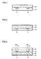
- FIG. 6is a cross-sectional view showing the manufacturing method of the semiconductor device of the conventional art.
- FIG. 7is a cross-sectional view showing the semiconductor device and the manufacturing method thereof of the conventional art.
- a pad electrode 51is formed on a front surface of a semiconductor substrate 50 formed with an electronic device (not shown), extending from the electronic device.
- a support substrate 60is further formed on the front surface of the semiconductor substrate 50 .
- This support substrate 60is made of, for example, a silicon substrate, a glass substrate, a ceramic substrate, or a metal substrate, supporting the semiconductor substrate 50 and preventing the semiconductor substrate 50 from cracking or warping.
- a back surface of the semiconductor substrate 50 supported by the support substrate 60is ground.
- the semiconductor substrate 50is thinned to have a predetermined thickness by this backgrinding process.
- the semiconductor substrate 50is formed with a via hole 52 penetrating from its back surface to the pad electrode 51 .
- a wiring layer 53is formed in the via hole 52 , being electrically connected with the pad electrode 51 .
- an insulation film(not shown) is formed between the semiconductor substrate 50 and the wiring layer 53 .
- a protection layer 54is formed on the wiring layer 53 so as to partially expose the wiring layer 53 .
- a conductive terminal 55is formed, which can be connected with an external printed circuit board and so on.
- dicingis performed along a dicing line (not shown) to separate the semiconductor substrate 50 into semiconductor dies 50 A. Then, the support substrate 60 attached to the front surface of the semiconductor die 50 A is peeled off or removed, thereby completing the package type semiconductor device.
- the relevant technologyis disclosed in the Japanese Patent Application Publication No. 2003-309221.
- the support substrate 60 used for supporting the semiconductor substrate 50 in the backgrinding process or the forming process of the via hole 52need be removed from the semiconductor die 50 A after the processes. This causes a problem of making a manufacturing method of the semiconductor device complex and increasing a manufacturing cost.
- the semiconductor die 50 Ais not sufficiently protected (from moisture permeation from outside and the like). This causes a problem of decreasing reliability of the semiconductor die.
- the front surface of the semiconductor die 50 A (or the semiconductor substrate 50 )is processed again for protecting the semiconductor die 50 A. This causes a problem of making the manufacturing method complex and increasing the manufacturing cost.
- the Inventionprovides a semiconductor device that includes a semiconductor die having a first surface and second surface, and a pad electrode formed on the first surface. A via hole is formed between the pad electrode and the second surface.
- the devicealso includes a first protection layer attached to the first surface so as to cover the pad electrode, an insulation film disposed on an inside wall of the via hole, and a metal portion disposed in the via hole to be in contact with the pad electrode.
- the inventionalso provides a method of manufacturing a semiconductor device.
- the methodincludes providing a semiconductor substrate having a first surface and a second surface and including a pad electrode formed on the first surface, forming a first protection layer on the first surface to cover the pad electrode, forming a via hole from the second surface to reach the pad electrode, forming an insulation film on a sidewall of the via hole, and filling at least partially the via hole having the insulation film with a metal so that the metal is contact with the pad electrode, and cutting the semiconductor substrate so as to produce a semiconductor device having a corresponding portion of the first protection layer as a protection element of the semiconductor device.
- FIG. 1is a cross-sectional view showing a manufacturing method of a semiconductor device of an embodiment of the invention.
- FIG. 2is a cross-sectional view showing the manufacturing method of the semiconductor device of the embodiment of the invention.
- FIG. 3is a cross-sectional view showing the manufacturing method of the semiconductor device of the embodiment of the invention.
- FIG. 4is a cross-sectional view showing the manufacturing method of the semiconductor device of the embodiment of the invention.
- FIG. 5is a cross-sectional view showing the semiconductor device and the manufacturing method thereof of the embodiment of the invention.
- FIG. 6is a cross-sectional view showing a manufacturing method of a semiconductor device of a conventional art.
- FIG. 7is a cross-sectional view showing the semiconductor device and the manufacturing method thereof of the conventional art.
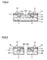
- FIGS. 1 to 5are cross-sectional views showing the manufacturing method of the semiconductor device of the embodiment. It is noted that FIGS. 1 to 5 show a portion near a dicing line (not shown) in a semiconductor substrate forming the semiconductor device.
- a semiconductor substrate 10 formed with an electronic deviceis prepared as shown in FIG. 1 .
- the electronic device (not shown)is formed on a front surface of the semiconductor substrate 10 .
- a pad electrode 11is formed on the front surface of the semiconductor substrate 10 , extending from the electronic device (not shown), which is also formed on the front surface of the semiconductor substrate 10 .
- the pad electrode 11is covered with a passivation film (not shown) made of silicon nitride or the like.
- a first protection layer 20is formed over the front surface of the semiconductor substrate 10 including on the electronic device (not shown) and on the pad electrode 11 .
- the first protection layer 20has a function of protecting the front surface of the semiconductor substrate 10 including the electronic device (not shown) and the pad electrode 11 and supporting the semiconductor substrate 10 .
- the first protection layer 20has a predetermined thickness that can support the semiconductor substrate 10 .
- the predetermined thickness of the first protection layer 20is not limited particularly, it is preferable to have the same thickness or substantially the same thickness as that of the semiconductor substrate 10 .
- the predetermined thicknesscan be the thickness that can support the semiconductor substrate 10 after a backgrinding process described below is performed to a back surface of the semiconductor substrate 10 .
- the first protection layer 20is formed by coating epoxy resin, for example, so as to have the predetermined thickness.
- the first protection layer 20can be formed of any material besides the epoxy resin even if the material is transparent, semi-transparent, or opaque, as long as the material can protect the front surface of the semiconductor substrate 10 including the electronic device (not shown) and the pad electrode 11 and support the semiconductor substrate 10 .
- the first protection layer 20can be formed of a material of a resist layer used for patterning and the like in a general manufacturing method of a semiconductor device.
- the first protection layer 20 and the resist layercan be formed of the same material. This enables the formation of the first protection layer 20 without making a manufacturing process complex and with minimizing a manufacturing cost.
- a protection tape 21 formed of a conductive materialis attached to the front surface of the first protection layer 20 as shown in FIG. 2 .
- This protection tape 21is provided for keeping the semiconductor substrate 10 on a conveying device (not shown) such as an electrostatic chuck by electrostatic attachment when the semiconductor substrate 10 is moved or inverted by the conveying device (not shown).
- the protection tape 21can be omitted when the semiconductor substrate 10 is moved or inverted by a mechanical conveying device such as a clamper.
- the front and back surfaces of the semiconductor substrate 10are inverted so that a process can be performed to the back surface of the semiconductor substrate 10 , as shown in FIG. 3 .
- the back surface of the semiconductor substrate 10is ground to have a predetermined thickness. That is, the backgrinding process is performed.
- the semiconductor substrate 10is protected and supported by the first protection layer 20 formed on the front surface thereof, cracking or warping of the semiconductor substrate 10 can be minimized even in a case where the thickness of the semiconductor substrate 10 is 130 ⁇ m or less, for example, when the backgrinding process is performed thereto. Furthermore, deterioration of electric characteristics of the electronic device (not shown) formed on the front surface of the semiconductor substrate 10 can be minimized.
- a resist layer 30is formed on the back surface of the semiconductor substrate 10 .
- the resist layer 30has an opening 30 a on a part of the back surface of the semiconductor substrate 10 corresponding to the pad electrode 11 .
- the semiconductor substrate 10is etched using this resist layer 30 as a mask.
- a via hole 12is formed penetrating the semiconductor substrate 10 from its back surface to the pad electrode 11 .
- an oxide film INSis formed on a sidewall of the via hole 12 and on the back surface of the semiconductor substrate 10 , exposing a bottom portion of the via hole 12 , as shown in FIG. 4 .
- a wiring layer 13 formed of, for example, metal such as Cu (copper)is formed on a region from the via hole 12 to the back surface of the semiconductor substrate 10 .
- This wiring layer 13is electrically connected with the pad electrode 11 exposed at the bottom portion of the via hole 12 .
- the wiring layer 13can be formed only in the via hole 12 without extending to the back surface of the semiconductor die.
- a second protection layer 14is formed over the back surface of the semiconductor substrate 10 including on the wiring layer 13 . Then, a predetermined part of the second protection layer 14 is selectively removed to form an opening 14 a exposing a part of the wiring layer 13 and to remove the second protection layer 14 in a region near the dicing line (not shown). Then, a conductive terminal 15 for connecting the semiconductor device to an external printed circuit board and the like is formed on the wiring layer 13 exposed at the opening 14 a . It is noted that the semiconductor device of the embodiment is not necessarily of BGA type, and the conductive terminal 15 can be omitted when the semiconductor device is of LGA (land grid array) type.
- the semiconductor die 10 A(the semiconductor substrate 10 in the manufacturing process) can be supported and protected as described above.
- the semiconductor die 10 Ais formed having a small thickness (e.g. 130 ⁇ m or less)
- the first protection layer 20effectively functions as a support layer necessary in the backgrinding process.
- the first protection layer 20has a function of protecting the semiconductor die 10 A, the first protection layer 20 need not be removed in the manufacturing process. Therefore, the manufacturing process of the package type semiconductor device can be performed more simply than conventional, so that the manufacturing cost can be minimized. Furthermore, since the front surface of the semiconductor die 10 A is protected by the first protection layer 20 , outside moisture can be prevented from permeating the semiconductor die 10 A through the front surface.
- the reliabilitycan be improved without making the manufacturing process complex and with minimizing the manufacturing cost.
Landscapes
- Engineering & Computer Science (AREA)
- Microelectronics & Electronic Packaging (AREA)
- Physics & Mathematics (AREA)
- Condensed Matter Physics & Semiconductors (AREA)
- General Physics & Mathematics (AREA)
- Computer Hardware Design (AREA)
- Power Engineering (AREA)
- Internal Circuitry In Semiconductor Integrated Circuit Devices (AREA)
- Mechanical Treatment Of Semiconductor (AREA)
- Dicing (AREA)
- Encapsulation Of And Coatings For Semiconductor Or Solid State Devices (AREA)
Abstract
Description
Claims (8)
Applications Claiming Priority (2)
| Application Number | Priority Date | Filing Date | Title |
|---|---|---|---|
| JP2004130676AJP4746847B2 (en) | 2004-04-27 | 2004-04-27 | Manufacturing method of semiconductor device |
| JP2004-130676 | 2004-04-27 |
Publications (2)
| Publication Number | Publication Date |
|---|---|
| US20050248030A1 US20050248030A1 (en) | 2005-11-10 |
| US7511320B2true US7511320B2 (en) | 2009-03-31 |
Family
ID=35238713
Family Applications (1)
| Application Number | Title | Priority Date | Filing Date |
|---|---|---|---|
| US11/111,999Active2027-04-01US7511320B2 (en) | 2004-04-27 | 2005-04-22 | Semiconductor device and manufacturing method of the same |
Country Status (5)
| Country | Link |
|---|---|
| US (1) | US7511320B2 (en) |
| JP (1) | JP4746847B2 (en) |
| KR (1) | KR100689133B1 (en) |
| CN (1) | CN100380646C (en) |
| TW (1) | TWI269413B (en) |
Families Citing this family (8)
| Publication number | Priority date | Publication date | Assignee | Title |
|---|---|---|---|---|
| TWI272683B (en)* | 2004-05-24 | 2007-02-01 | Sanyo Electric Co | Semiconductor device and manufacturing method thereof |
| JP4376715B2 (en)* | 2004-07-16 | 2009-12-02 | 三洋電機株式会社 | Manufacturing method of semiconductor device |
| JP2009158830A (en)* | 2007-12-27 | 2009-07-16 | Sanyo Electric Co Ltd | Substrate for mounting element and manufacturing method thereof, semiconductor module and manufacturing method thereof, and portable equipment |
| DE102009029184A1 (en)* | 2009-09-03 | 2011-03-10 | Robert Bosch Gmbh | Production method for a capped micromechanical component, corresponding micromechanical component and cap for a micromechanical component |
| JP5232185B2 (en)* | 2010-03-05 | 2013-07-10 | 株式会社東芝 | Manufacturing method of semiconductor device |
| JP2012009545A (en)* | 2010-06-23 | 2012-01-12 | Toshiba Corp | Semiconductor device manufacturing method |
| TWI426584B (en)* | 2010-12-22 | 2014-02-11 | 矽品精密工業股份有限公司 | Semiconductor package and method of forming same |
| US9553021B2 (en)* | 2012-09-03 | 2017-01-24 | Infineon Technologies Ag | Method for processing a wafer and method for dicing a wafer |
Citations (4)
| Publication number | Priority date | Publication date | Assignee | Title |
|---|---|---|---|---|
| KR20010055255A (en) | 1999-12-10 | 2001-07-04 | 마이클 디. 오브라이언 | semiconductor package and its manufacturing method |
| US6498389B1 (en) | 2001-07-16 | 2002-12-24 | Samsung Electronics Co., Ltd. | Ultra-thin semiconductor package device using a support tape |
| JP2003309221A (en) | 2002-04-15 | 2003-10-31 | Sanyo Electric Co Ltd | Method of manufacturing semiconductor device |
| US6847066B2 (en) | 2000-08-11 | 2005-01-25 | Oki Electric Industry Co., Ltd. | Semiconductor device |
Family Cites Families (6)
| Publication number | Priority date | Publication date | Assignee | Title |
|---|---|---|---|---|
| JP2000195861A (en)* | 1998-12-25 | 2000-07-14 | Texas Instr Japan Ltd | Semiconductor device and manufacturing method thereof |
| US6379982B1 (en)* | 2000-08-17 | 2002-04-30 | Micron Technology, Inc. | Wafer on wafer packaging and method of fabrication for full-wafer burn-in and testing |
| JP2002305234A (en)* | 2001-04-05 | 2002-10-18 | Matsushita Electric Ind Co Ltd | Silicon wafer backside etching method and silicon wafer protection tape |
| JP2003017495A (en)* | 2001-07-04 | 2003-01-17 | Matsushita Electric Ind Co Ltd | Semiconductor device and method of manufacturing the same |
| JP3612310B2 (en)* | 2002-06-18 | 2005-01-19 | 株式会社東芝 | Semiconductor device |
| JP4215571B2 (en)* | 2002-06-18 | 2009-01-28 | 三洋電機株式会社 | Manufacturing method of semiconductor device |
- 2004
- 2004-04-27JPJP2004130676Apatent/JP4746847B2/ennot_activeExpired - Fee Related
- 2005
- 2005-04-22USUS11/111,999patent/US7511320B2/enactiveActive
- 2005-04-25CNCNB2005100674749Apatent/CN100380646C/ennot_activeExpired - Lifetime
- 2005-04-26KRKR1020050034397Apatent/KR100689133B1/ennot_activeExpired - Fee Related
- 2005-04-26TWTW094113209Apatent/TWI269413B/ennot_activeIP Right Cessation
Patent Citations (5)
| Publication number | Priority date | Publication date | Assignee | Title |
|---|---|---|---|---|
| KR20010055255A (en) | 1999-12-10 | 2001-07-04 | 마이클 디. 오브라이언 | semiconductor package and its manufacturing method |
| US6847066B2 (en) | 2000-08-11 | 2005-01-25 | Oki Electric Industry Co., Ltd. | Semiconductor device |
| US6498389B1 (en) | 2001-07-16 | 2002-12-24 | Samsung Electronics Co., Ltd. | Ultra-thin semiconductor package device using a support tape |
| KR20030006844A (en) | 2001-07-16 | 2003-01-23 | 삼성전자 주식회사 | Ultra-Thin Semiconductor Package Device Using a Support Tape |
| JP2003309221A (en) | 2002-04-15 | 2003-10-31 | Sanyo Electric Co Ltd | Method of manufacturing semiconductor device |
Also Published As
| Publication number | Publication date |
|---|---|
| TW200536067A (en) | 2005-11-01 |
| JP4746847B2 (en) | 2011-08-10 |
| KR100689133B1 (en) | 2007-03-08 |
| KR20060046697A (en) | 2006-05-17 |
| CN1691318A (en) | 2005-11-02 |
| TWI269413B (en) | 2006-12-21 |
| CN100380646C (en) | 2008-04-09 |
| US20050248030A1 (en) | 2005-11-10 |
| JP2005317578A (en) | 2005-11-10 |
Similar Documents
| Publication | Publication Date | Title |
|---|---|---|
| US11961867B2 (en) | Electronic device package and fabricating method thereof | |
| US10157811B2 (en) | Chip package and method for forming the same | |
| JP4307284B2 (en) | Manufacturing method of semiconductor device | |
| US7312521B2 (en) | Semiconductor device with holding member | |
| KR100659625B1 (en) | Semiconductor device and method for manufacturing the same | |
| US7732925B2 (en) | Semiconductor device and manufacturing method thereof | |
| US7944015B2 (en) | Semiconductor device and method of manufacturing the same | |
| US9337097B2 (en) | Chip package and method for forming the same | |
| US8766408B2 (en) | Semiconductor device and manufacturing method thereof | |
| US8018032B2 (en) | Silicon substrate and chip package structure with silicon base having stepped recess for accommodating chip | |
| US7416920B2 (en) | Semiconductor device protective structure and method for fabricating the same | |
| EP1478021A1 (en) | Semiconductor device and manufacturing method thereof | |
| US7511320B2 (en) | Semiconductor device and manufacturing method of the same | |
| US7557017B2 (en) | Method of manufacturing semiconductor device with two-step etching of layer | |
| JP4845986B2 (en) | Semiconductor device | |
| KR100591128B1 (en) | Semiconductor device and manufacturing method thereof | |
| JP2004327748A (en) | Semiconductor device and manufacturing method thereof |
Legal Events
| Date | Code | Title | Description |
|---|---|---|---|
| AS | Assignment | Owner name:SANYO ELECTRIC CO., LTD., JAPAN Free format text:ASSIGNMENT OF ASSIGNORS INTEREST;ASSIGNOR:OCHIAI, ISAO;REEL/FRAME:016797/0265 Effective date:20050707 | |
| FEPP | Fee payment procedure | Free format text:PAYOR NUMBER ASSIGNED (ORIGINAL EVENT CODE: ASPN); ENTITY STATUS OF PATENT OWNER: LARGE ENTITY | |
| STCF | Information on status: patent grant | Free format text:PATENTED CASE | |
| FEPP | Fee payment procedure | Free format text:PAYOR NUMBER ASSIGNED (ORIGINAL EVENT CODE: ASPN); ENTITY STATUS OF PATENT OWNER: LARGE ENTITY Free format text:PAYER NUMBER DE-ASSIGNED (ORIGINAL EVENT CODE: RMPN); ENTITY STATUS OF PATENT OWNER: LARGE ENTITY | |
| AS | Assignment | Owner name:SEMICONDUCTOR COMPONENTS INDUSTRIES, LLC, ARIZONA Free format text:ASSIGNMENT OF ASSIGNORS INTEREST;ASSIGNOR:SANYO ELECTRIC CO., LTD.;REEL/FRAME:026594/0385 Effective date:20110101 | |
| FPAY | Fee payment | Year of fee payment:4 | |
| AS | Assignment | Owner name:SEMICONDUCTOR COMPONENTS INDUSTRIES, LLC, ARIZONA Free format text:CORRECTIVE ASSIGNMENT TO CORRECT THE INCORRECT #12/577882 PREVIOUSLY RECORDED ON REEL 026594 FRAME 0385. ASSIGNOR(S) HEREBY CONFIRMS THE ASSIGNMENT;ASSIGNOR:SANYO ELECTRIC CO., LTD;REEL/FRAME:032836/0342 Effective date:20110101 | |
| AS | Assignment | Owner name:SEMICONDUCTOR COMPONENTS INDUSTRIES, LLC, ARIZONA Free format text:ASSIGNMENT OF ASSIGNORS INTEREST;ASSIGNOR:KANTO SANYO SEMICONDUCTOR CO., LTD.;REEL/FRAME:033713/0296 Effective date:20140910 | |
| AS | Assignment | Owner name:DEUTSCHE BANK AG NEW YORK BRANCH, NEW YORK Free format text:SECURITY INTEREST;ASSIGNOR:SEMICONDUCTOR COMPONENTS INDUSTRIES, LLC;REEL/FRAME:038620/0087 Effective date:20160415 | |
| AS | Assignment | Owner name:DEUTSCHE BANK AG NEW YORK BRANCH, AS COLLATERAL AG Free format text:CORRECTIVE ASSIGNMENT TO CORRECT THE INCORRECT PATENT NUMBER 5859768 AND TO RECITE COLLATERAL AGENT ROLE OF RECEIVING PARTY IN THE SECURITY INTEREST PREVIOUSLY RECORDED ON REEL 038620 FRAME 0087. ASSIGNOR(S) HEREBY CONFIRMS THE SECURITY INTEREST;ASSIGNOR:SEMICONDUCTOR COMPONENTS INDUSTRIES, LLC;REEL/FRAME:039853/0001 Effective date:20160415 Owner name:DEUTSCHE BANK AG NEW YORK BRANCH, AS COLLATERAL AGENT, NEW YORK Free format text:CORRECTIVE ASSIGNMENT TO CORRECT THE INCORRECT PATENT NUMBER 5859768 AND TO RECITE COLLATERAL AGENT ROLE OF RECEIVING PARTY IN THE SECURITY INTEREST PREVIOUSLY RECORDED ON REEL 038620 FRAME 0087. ASSIGNOR(S) HEREBY CONFIRMS THE SECURITY INTEREST;ASSIGNOR:SEMICONDUCTOR COMPONENTS INDUSTRIES, LLC;REEL/FRAME:039853/0001 Effective date:20160415 | |
| FPAY | Fee payment | Year of fee payment:8 | |
| MAFP | Maintenance fee payment | Free format text:PAYMENT OF MAINTENANCE FEE, 12TH YEAR, LARGE ENTITY (ORIGINAL EVENT CODE: M1553); ENTITY STATUS OF PATENT OWNER: LARGE ENTITY Year of fee payment:12 | |
| AS | Assignment | Owner name:FAIRCHILD SEMICONDUCTOR CORPORATION, ARIZONA Free format text:RELEASE OF SECURITY INTEREST IN PATENTS RECORDED AT REEL 038620, FRAME 0087;ASSIGNOR:DEUTSCHE BANK AG NEW YORK BRANCH, AS COLLATERAL AGENT;REEL/FRAME:064070/0001 Effective date:20230622 Owner name:SEMICONDUCTOR COMPONENTS INDUSTRIES, LLC, ARIZONA Free format text:RELEASE OF SECURITY INTEREST IN PATENTS RECORDED AT REEL 038620, FRAME 0087;ASSIGNOR:DEUTSCHE BANK AG NEW YORK BRANCH, AS COLLATERAL AGENT;REEL/FRAME:064070/0001 Effective date:20230622 |