US7510943B2 - Semiconductor devices and methods of manufacture thereof - Google Patents
Semiconductor devices and methods of manufacture thereofDownload PDFInfo
- Publication number
- US7510943B2 US7510943B2US11/305,567US30556705AUS7510943B2US 7510943 B2US7510943 B2US 7510943B2US 30556705 AUS30556705 AUS 30556705AUS 7510943 B2US7510943 B2US 7510943B2
- Authority
- US
- United States
- Prior art keywords
- dopant
- workpiece
- region
- gate dielectric
- gate
- Prior art date
- Legal status (The legal status is an assumption and is not a legal conclusion. Google has not performed a legal analysis and makes no representation as to the accuracy of the status listed.)
- Expired - Fee Related, expires
Links
- 238000000034methodMethods0.000titleclaimsdescription88
- 238000004519manufacturing processMethods0.000titleclaimsdescription33
- 239000004065semiconductorSubstances0.000titleclaimsdescription23
- 239000002019doping agentSubstances0.000claimsabstractdescription227
- 239000000463materialSubstances0.000claimsabstractdescription171
- 229910000897Babbitt (metal)Inorganic materials0.000claimsabstractdescription115
- 229910052751metalInorganic materials0.000claimsabstractdescription47
- 239000002184metalSubstances0.000claimsabstractdescription47
- 239000003989dielectric materialSubstances0.000claimsdescription129
- 238000000151depositionMethods0.000claimsdescription19
- 125000006850spacer groupChemical group0.000claimsdescription17
- 230000000873masking effectEffects0.000claimsdescription14
- 229910021420polycrystalline siliconInorganic materials0.000claimsdescription13
- 229920005591polysiliconPolymers0.000claimsdescription13
- 238000002513implantationMethods0.000claimsdescription12
- 238000009792diffusion processMethods0.000claimsdescription7
- 150000002500ionsChemical class0.000claimsdescription6
- 238000000059patterningMethods0.000claimsdescription4
- 230000000295complement effectEffects0.000claimsdescription3
- 229910044991metal oxideInorganic materials0.000claimsdescription3
- 150000004706metal oxidesChemical class0.000claimsdescription3
- 238000000137annealingMethods0.000claims6
- 150000002739metalsChemical class0.000abstractdescription10
- 239000010410layerSubstances0.000description85
- 230000008569processEffects0.000description44
- 229920002120photoresistant polymerPolymers0.000description25
- 239000011810insulating materialSubstances0.000description16
- VYPSYNLAJGMNEJ-UHFFFAOYSA-NSilicium dioxideChemical compoundO=[Si]=OVYPSYNLAJGMNEJ-UHFFFAOYSA-N0.000description13
- 230000008901benefitEffects0.000description12
- XUIMIQQOPSSXEZ-UHFFFAOYSA-NSiliconChemical compound[Si]XUIMIQQOPSSXEZ-UHFFFAOYSA-N0.000description11
- 229910052782aluminiumInorganic materials0.000description11
- 229910052757nitrogenInorganic materials0.000description11
- 229910052726zirconiumInorganic materials0.000description11
- 230000006870functionEffects0.000description10
- 229910052735hafniumInorganic materials0.000description10
- 229910052719titaniumInorganic materials0.000description10
- 229910052710siliconInorganic materials0.000description8
- 239000010703siliconSubstances0.000description8
- -1HfSiOXInorganic materials0.000description7
- 238000005229chemical vapour depositionMethods0.000description7
- 230000009977dual effectEffects0.000description7
- 230000000694effectsEffects0.000description7
- 239000002356single layerSubstances0.000description7
- 229910052727yttriumInorganic materials0.000description7
- ITWBWJFEJCHKSN-UHFFFAOYSA-N1,4,7-triazonaneChemical compoundC1CNCCNCCN1ITWBWJFEJCHKSN-UHFFFAOYSA-N0.000description6
- 229910052796boronInorganic materials0.000description6
- 238000005468ion implantationMethods0.000description6
- 238000001459lithographyMethods0.000description6
- 238000005240physical vapour depositionMethods0.000description6
- WOCIAKWEIIZHES-UHFFFAOYSA-Nruthenium(iv) oxideChemical compoundO=[Ru]=OWOCIAKWEIIZHES-UHFFFAOYSA-N0.000description6
- 239000000377silicon dioxideSubstances0.000description6
- ZOXJGFHDIHLPTG-UHFFFAOYSA-NBoronChemical compound[B]ZOXJGFHDIHLPTG-UHFFFAOYSA-N0.000description5
- 238000000231atomic layer depositionMethods0.000description5
- 238000002955isolationMethods0.000description5
- 150000004767nitridesChemical class0.000description5
- 229910052814silicon oxideInorganic materials0.000description5
- GWEVSGVZZGPLCZ-UHFFFAOYSA-NTitan oxideChemical compoundO=[Ti]=OGWEVSGVZZGPLCZ-UHFFFAOYSA-N0.000description4
- MCMNRKCIXSYSNV-UHFFFAOYSA-NZirconium dioxideChemical compoundO=[Zr]=OMCMNRKCIXSYSNV-UHFFFAOYSA-N0.000description4
- 230000015572biosynthetic processEffects0.000description4
- 229910052681coesiteInorganic materials0.000description4
- 229910052906cristobaliteInorganic materials0.000description4
- 230000003247decreasing effectEffects0.000description4
- 230000000737periodic effectEffects0.000description4
- 229910052698phosphorusInorganic materials0.000description4
- 241000894007speciesSpecies0.000description4
- 229910052682stishoviteInorganic materials0.000description4
- 239000000758substrateSubstances0.000description4
- 229910052715tantalumInorganic materials0.000description4
- 229910052905tridymiteInorganic materials0.000description4
- 229910019044CoSixInorganic materials0.000description3
- 229910004542HfNInorganic materials0.000description3
- 229910003322NiCuInorganic materials0.000description3
- 229910005889NiSixInorganic materials0.000description3
- 241001521328RutaSpecies0.000description3
- 235000003976RutaNutrition0.000description3
- 229910020776SixNyInorganic materials0.000description3
- 229910004166TaNInorganic materials0.000description3
- 229910004200TaSiNInorganic materials0.000description3
- 229910010037TiAlNInorganic materials0.000description3
- 229910008482TiSiNInorganic materials0.000description3
- 229910008486TiSixInorganic materials0.000description3
- ATJFFYVFTNAWJD-UHFFFAOYSA-NTinChemical compound[Sn]ATJFFYVFTNAWJD-UHFFFAOYSA-N0.000description3
- 229910008807WSiNInorganic materials0.000description3
- 229910052787antimonyInorganic materials0.000description3
- 229910052785arsenicInorganic materials0.000description3
- 239000004020conductorSubstances0.000description3
- 238000005530etchingMethods0.000description3
- 238000001912gas jet depositionMethods0.000description3
- 229910052741iridiumInorganic materials0.000description3
- HTXDPTMKBJXEOW-UHFFFAOYSA-Niridium(IV) oxideInorganic materialsO=[Ir]=OHTXDPTMKBJXEOW-UHFFFAOYSA-N0.000description3
- QRXWMOHMRWLFEY-UHFFFAOYSA-NisoniazideChemical compoundNNC(=O)C1=CC=NC=C1QRXWMOHMRWLFEY-UHFFFAOYSA-N0.000description3
- 239000000203mixtureSubstances0.000description3
- 229910001000nickel titaniumInorganic materials0.000description3
- 229910052763palladiumInorganic materials0.000description3
- 238000000623plasma-assisted chemical vapour depositionMethods0.000description3
- 229910052697platinumInorganic materials0.000description3
- 229910052702rheniumInorganic materials0.000description3
- 229910052703rhodiumInorganic materials0.000description3
- 235000005806rutaNutrition0.000description3
- 229910052707rutheniumInorganic materials0.000description3
- 229910052721tungstenInorganic materials0.000description3
- XKRFYHLGVUSROY-UHFFFAOYSA-NArgonChemical compound[Ar]XKRFYHLGVUSROY-UHFFFAOYSA-N0.000description2
- QYEXBYZXHDUPRC-UHFFFAOYSA-NB#[Ti]#BChemical compoundB#[Ti]#BQYEXBYZXHDUPRC-UHFFFAOYSA-N0.000description2
- 229910052684CeriumInorganic materials0.000description2
- 229910052692DysprosiumInorganic materials0.000description2
- 229910052691ErbiumInorganic materials0.000description2
- 229910052693EuropiumInorganic materials0.000description2
- 229910052688GadoliniumInorganic materials0.000description2
- 229910052689HolmiumInorganic materials0.000description2
- 229910002244LaAlO3Inorganic materials0.000description2
- 229910052779NeodymiumInorganic materials0.000description2
- PXHVJJICTQNCMI-UHFFFAOYSA-NNickelChemical compound[Ni]PXHVJJICTQNCMI-UHFFFAOYSA-N0.000description2
- 229910052777PraseodymiumInorganic materials0.000description2
- 229910052772SamariumInorganic materials0.000description2
- 229910004541SiNInorganic materials0.000description2
- 229910052771TerbiumInorganic materials0.000description2
- 229910052775ThuliumInorganic materials0.000description2
- 229910033181TiB2Inorganic materials0.000description2
- 229910010252TiO3Inorganic materials0.000description2
- 229910008812WSiInorganic materials0.000description2
- PNEYBMLMFCGWSK-UHFFFAOYSA-Naluminium oxideInorganic materials[O-2].[O-2].[O-2].[Al+3].[Al+3]PNEYBMLMFCGWSK-UHFFFAOYSA-N0.000description2
- WATWJIUSRGPENY-UHFFFAOYSA-Nantimony atomChemical compound[Sb]WATWJIUSRGPENY-UHFFFAOYSA-N0.000description2
- CETPSERCERDGAM-UHFFFAOYSA-Nceric oxideChemical compoundO=[Ce]=OCETPSERCERDGAM-UHFFFAOYSA-N0.000description2
- 229910000422cerium(IV) oxideInorganic materials0.000description2
- 229910052593corundumInorganic materials0.000description2
- 239000007772electrode materialSubstances0.000description2
- 238000000609electron-beam lithographyMethods0.000description2
- CJNBYAVZURUTKZ-UHFFFAOYSA-Nhafnium(IV) oxideInorganic materialsO=[Hf]=OCJNBYAVZURUTKZ-UHFFFAOYSA-N0.000description2
- BHEPBYXIRTUNPN-UHFFFAOYSA-Nhydridophosphorus(.) (triplet)Chemical compound[PH]BHEPBYXIRTUNPN-UHFFFAOYSA-N0.000description2
- 229910052747lanthanoidInorganic materials0.000description2
- 150000002602lanthanoidsChemical class0.000description2
- 229910052746lanthanumInorganic materials0.000description2
- MRELNEQAGSRDBK-UHFFFAOYSA-Nlanthanum oxideInorganic materials[O-2].[O-2].[O-2].[La+3].[La+3]MRELNEQAGSRDBK-UHFFFAOYSA-N0.000description2
- KTUFCUMIWABKDW-UHFFFAOYSA-Noxo(oxolanthaniooxy)lanthanumChemical compoundO=[La]O[La]=OKTUFCUMIWABKDW-UHFFFAOYSA-N0.000description2
- 230000009467reductionEffects0.000description2
- 229910052706scandiumInorganic materials0.000description2
- 235000012239silicon dioxideNutrition0.000description2
- 239000000126substanceSubstances0.000description2
- PBCFLUZVCVVTBY-UHFFFAOYSA-Ntantalum pentoxideInorganic materialsO=[Ta](=O)O[Ta](=O)=OPBCFLUZVCVVTBY-UHFFFAOYSA-N0.000description2
- 229910001845yogo sapphireInorganic materials0.000description2
- 229910001218Gallium arsenideInorganic materials0.000description1
- 229910003862HfB2Inorganic materials0.000description1
- 229910052766LawrenciumInorganic materials0.000description1
- 229910052765LutetiumInorganic materials0.000description1
- CBENFWSGALASAD-UHFFFAOYSA-NOzoneChemical compound[O-][O+]=OCBENFWSGALASAD-UHFFFAOYSA-N0.000description1
- 229910000577Silicon-germaniumInorganic materials0.000description1
- 229910052769YtterbiumInorganic materials0.000description1
- 229910007948ZrB2Inorganic materials0.000description1
- 229910006248ZrSb2Inorganic materials0.000description1
- 230000004913activationEffects0.000description1
- 230000004075alterationEffects0.000description1
- XAGFODPZIPBFFR-UHFFFAOYSA-NaluminiumChemical compound[Al]XAGFODPZIPBFFR-UHFFFAOYSA-N0.000description1
- 229910052786argonInorganic materials0.000description1
- RQNWIZPPADIBDY-UHFFFAOYSA-Narsenic atomChemical compound[As]RQNWIZPPADIBDY-UHFFFAOYSA-N0.000description1
- 230000009286beneficial effectEffects0.000description1
- VWZIXVXBCBBRGP-UHFFFAOYSA-Nboron;zirconiumChemical compoundB#[Zr]#BVWZIXVXBCBBRGP-UHFFFAOYSA-N0.000description1
- 238000004140cleaningMethods0.000description1
- 150000001875compoundsChemical class0.000description1
- 238000010276constructionMethods0.000description1
- 239000000356contaminantSubstances0.000description1
- 230000008021depositionEffects0.000description1
- 238000005137deposition processMethods0.000description1
- 238000005566electron beam evaporationMethods0.000description1
- 238000005516engineering processMethods0.000description1
- 230000005669field effectEffects0.000description1
- 239000007943implantSubstances0.000description1
- 239000012212insulatorSubstances0.000description1
- 229910021421monocrystalline siliconInorganic materials0.000description1
- 229910052759nickelInorganic materials0.000description1
- 229910021334nickel silicideInorganic materials0.000description1
- RUFLMLWJRZAWLJ-UHFFFAOYSA-Nnickel silicideChemical compound[Ni]=[Si]=[Ni]RUFLMLWJRZAWLJ-UHFFFAOYSA-N0.000description1
- 230000035515penetrationEffects0.000description1
- 238000005389semiconductor device fabricationMethods0.000description1
- 238000006467substitution reactionMethods0.000description1
Images


Classifications
- H—ELECTRICITY
- H10—SEMICONDUCTOR DEVICES; ELECTRIC SOLID-STATE DEVICES NOT OTHERWISE PROVIDED FOR
- H10D—INORGANIC ELECTRIC SEMICONDUCTOR DEVICES
- H10D62/00—Semiconductor bodies, or regions thereof, of devices having potential barriers
- H10D62/01—Manufacture or treatment
- H10D62/021—Forming source or drain recesses by etching e.g. recessing by etching and then refilling
- H—ELECTRICITY
- H01—ELECTRIC ELEMENTS
- H01L—SEMICONDUCTOR DEVICES NOT COVERED BY CLASS H10
- H01L21/00—Processes or apparatus adapted for the manufacture or treatment of semiconductor or solid state devices or of parts thereof
- H01L21/02—Manufacture or treatment of semiconductor devices or of parts thereof
- H01L21/04—Manufacture or treatment of semiconductor devices or of parts thereof the devices having potential barriers, e.g. a PN junction, depletion layer or carrier concentration layer
- H01L21/18—Manufacture or treatment of semiconductor devices or of parts thereof the devices having potential barriers, e.g. a PN junction, depletion layer or carrier concentration layer the devices having semiconductor bodies comprising elements of Group IV of the Periodic Table or AIIIBV compounds with or without impurities, e.g. doping materials
- H01L21/22—Diffusion of impurity materials, e.g. doping materials, electrode materials, into or out of a semiconductor body, or between semiconductor regions; Interactions between two or more impurities; Redistribution of impurities
- H01L21/225—Diffusion of impurity materials, e.g. doping materials, electrode materials, into or out of a semiconductor body, or between semiconductor regions; Interactions between two or more impurities; Redistribution of impurities using diffusion into or out of a solid from or into a solid phase, e.g. a doped oxide layer
- H01L21/2251—Diffusion into or out of group IV semiconductors
- H01L21/2252—Diffusion into or out of group IV semiconductors using predeposition of impurities into the semiconductor surface, e.g. from a gaseous phase
- H01L21/2253—Diffusion into or out of group IV semiconductors using predeposition of impurities into the semiconductor surface, e.g. from a gaseous phase by ion implantation
- H—ELECTRICITY
- H10—SEMICONDUCTOR DEVICES; ELECTRIC SOLID-STATE DEVICES NOT OTHERWISE PROVIDED FOR
- H10D—INORGANIC ELECTRIC SEMICONDUCTOR DEVICES
- H10D30/00—Field-effect transistors [FET]
- H10D30/01—Manufacture or treatment
- H10D30/021—Manufacture or treatment of FETs having insulated gates [IGFET]
- H10D30/0223—Manufacture or treatment of FETs having insulated gates [IGFET] having source and drain regions or source and drain extensions self-aligned to sides of the gate
- H10D30/0227—Manufacture or treatment of FETs having insulated gates [IGFET] having source and drain regions or source and drain extensions self-aligned to sides of the gate having both lightly-doped source and drain extensions and source and drain regions self-aligned to the sides of the gate, e.g. lightly-doped drain [LDD] MOSFET or double-diffused drain [DDD] MOSFET
- H—ELECTRICITY
- H10—SEMICONDUCTOR DEVICES; ELECTRIC SOLID-STATE DEVICES NOT OTHERWISE PROVIDED FOR
- H10D—INORGANIC ELECTRIC SEMICONDUCTOR DEVICES
- H10D84/00—Integrated devices formed in or on semiconductor substrates that comprise only semiconducting layers, e.g. on Si wafers or on GaAs-on-Si wafers
- H10D84/01—Manufacture or treatment
- H10D84/0123—Integrating together multiple components covered by H10D12/00 or H10D30/00, e.g. integrating multiple IGBTs
- H10D84/0126—Integrating together multiple components covered by H10D12/00 or H10D30/00, e.g. integrating multiple IGBTs the components including insulated gates, e.g. IGFETs
- H10D84/0165—Integrating together multiple components covered by H10D12/00 or H10D30/00, e.g. integrating multiple IGBTs the components including insulated gates, e.g. IGFETs the components including complementary IGFETs, e.g. CMOS devices
- H10D84/017—Manufacturing their source or drain regions, e.g. silicided source or drain regions
- H—ELECTRICITY
- H10—SEMICONDUCTOR DEVICES; ELECTRIC SOLID-STATE DEVICES NOT OTHERWISE PROVIDED FOR
- H10D—INORGANIC ELECTRIC SEMICONDUCTOR DEVICES
- H10D84/00—Integrated devices formed in or on semiconductor substrates that comprise only semiconducting layers, e.g. on Si wafers or on GaAs-on-Si wafers
- H10D84/01—Manufacture or treatment
- H10D84/0123—Integrating together multiple components covered by H10D12/00 or H10D30/00, e.g. integrating multiple IGBTs
- H10D84/0126—Integrating together multiple components covered by H10D12/00 or H10D30/00, e.g. integrating multiple IGBTs the components including insulated gates, e.g. IGFETs
- H10D84/0165—Integrating together multiple components covered by H10D12/00 or H10D30/00, e.g. integrating multiple IGBTs the components including insulated gates, e.g. IGFETs the components including complementary IGFETs, e.g. CMOS devices
- H10D84/0181—Manufacturing their gate insulating layers
- H—ELECTRICITY
- H10—SEMICONDUCTOR DEVICES; ELECTRIC SOLID-STATE DEVICES NOT OTHERWISE PROVIDED FOR
- H10D—INORGANIC ELECTRIC SEMICONDUCTOR DEVICES
- H10D84/00—Integrated devices formed in or on semiconductor substrates that comprise only semiconducting layers, e.g. on Si wafers or on GaAs-on-Si wafers
- H10D84/01—Manufacture or treatment
- H10D84/02—Manufacture or treatment characterised by using material-based technologies
- H10D84/03—Manufacture or treatment characterised by using material-based technologies using Group IV technology, e.g. silicon technology or silicon-carbide [SiC] technology
- H10D84/038—Manufacture or treatment characterised by using material-based technologies using Group IV technology, e.g. silicon technology or silicon-carbide [SiC] technology using silicon technology, e.g. SiGe
- H—ELECTRICITY
- H01—ELECTRIC ELEMENTS
- H01L—SEMICONDUCTOR DEVICES NOT COVERED BY CLASS H10
- H01L21/00—Processes or apparatus adapted for the manufacture or treatment of semiconductor or solid state devices or of parts thereof
- H01L21/02—Manufacture or treatment of semiconductor devices or of parts thereof
- H01L21/04—Manufacture or treatment of semiconductor devices or of parts thereof the devices having potential barriers, e.g. a PN junction, depletion layer or carrier concentration layer
- H01L21/18—Manufacture or treatment of semiconductor devices or of parts thereof the devices having potential barriers, e.g. a PN junction, depletion layer or carrier concentration layer the devices having semiconductor bodies comprising elements of Group IV of the Periodic Table or AIIIBV compounds with or without impurities, e.g. doping materials
- H01L21/28—Manufacture of electrodes on semiconductor bodies using processes or apparatus not provided for in groups H01L21/20 - H01L21/268
- H01L21/28008—Making conductor-insulator-semiconductor electrodes
- H01L21/28017—Making conductor-insulator-semiconductor electrodes the insulator being formed after the semiconductor body, the semiconductor being silicon
- H01L21/28158—Making the insulator
- H01L21/28167—Making the insulator on single crystalline silicon, e.g. using a liquid, i.e. chemical oxidation
- H01L21/28194—Making the insulator on single crystalline silicon, e.g. using a liquid, i.e. chemical oxidation by deposition, e.g. evaporation, ALD, CVD, sputtering, laser deposition
- H—ELECTRICITY
- H10—SEMICONDUCTOR DEVICES; ELECTRIC SOLID-STATE DEVICES NOT OTHERWISE PROVIDED FOR
- H10D—INORGANIC ELECTRIC SEMICONDUCTOR DEVICES
- H10D30/00—Field-effect transistors [FET]
- H10D30/60—Insulated-gate field-effect transistors [IGFET]
- H10D30/601—Insulated-gate field-effect transistors [IGFET] having lightly-doped drain or source extensions, e.g. LDD IGFETs or DDD IGFETs
- H—ELECTRICITY
- H10—SEMICONDUCTOR DEVICES; ELECTRIC SOLID-STATE DEVICES NOT OTHERWISE PROVIDED FOR
- H10D—INORGANIC ELECTRIC SEMICONDUCTOR DEVICES
- H10D64/00—Electrodes of devices having potential barriers
- H10D64/60—Electrodes characterised by their materials
- H10D64/66—Electrodes having a conductor capacitively coupled to a semiconductor by an insulator, e.g. MIS electrodes
- H10D64/68—Electrodes having a conductor capacitively coupled to a semiconductor by an insulator, e.g. MIS electrodes characterised by the insulator, e.g. by the gate insulator
- H10D64/691—Electrodes having a conductor capacitively coupled to a semiconductor by an insulator, e.g. MIS electrodes characterised by the insulator, e.g. by the gate insulator comprising metallic compounds, e.g. metal oxides or metal silicates
- H—ELECTRICITY
- H10—SEMICONDUCTOR DEVICES; ELECTRIC SOLID-STATE DEVICES NOT OTHERWISE PROVIDED FOR
- H10D—INORGANIC ELECTRIC SEMICONDUCTOR DEVICES
- H10D64/00—Electrodes of devices having potential barriers
- H10D64/60—Electrodes characterised by their materials
- H10D64/66—Electrodes having a conductor capacitively coupled to a semiconductor by an insulator, e.g. MIS electrodes
- H10D64/68—Electrodes having a conductor capacitively coupled to a semiconductor by an insulator, e.g. MIS electrodes characterised by the insulator, e.g. by the gate insulator
- H10D64/693—Electrodes having a conductor capacitively coupled to a semiconductor by an insulator, e.g. MIS electrodes characterised by the insulator, e.g. by the gate insulator the insulator comprising nitrogen, e.g. nitrides, oxynitrides or nitrogen-doped materials
Definitions
- the present inventionrelates generally to the fabrication of semiconductor devices, and more particularly to transistor devices and the fabrication thereof.
- Semiconductor devicesare used in a variety of electronic applications, such as personal computers, cell phones, digital cameras, and other electronic equipment, as examples. Semiconductor devices are typically fabricated by sequentially depositing insulating (or dielectric) layers, conductive layers and semiconductive layers of material over a semiconductor substrate, and patterning the various layers using lithography to form circuit components and elements thereon.
- a transistoris an element that is utilized extensively in semiconductor devices. There may be millions of transistors on a single integrated circuit (IC), for example.
- ICintegrated circuit
- a common type of transistor used in semiconductor device fabricationis a metal oxide semiconductor field effect transistor (MOSFET).
- CMOScomplementary metal oxide semiconductor
- the gate dielectric for MOSFET deviceshas in the past typically comprised silicon dioxide, which has a dielectric constant of about 3.9.
- silicon dioxidewhich has a dielectric constant of about 3.9.
- high k materialrefers to a dielectric material having a dielectric constant of about 4.0 or greater. If high k materials are successfully implemented in transistor designs, the effective oxide thickness of the gate dielectric is expected to be reduced, increasing device performance.
- CMOS devicesit is desirable to achieve a symmetric threshold voltage V t for the PMOS transistor and the NMOS transistor. If high k dielectric materials are used for the gate dielectric, a symmetric threshold voltage V t may not be achievable.
- junction depth X j and sheet resistance R sare required.
- the thicker the junction depth X jthe more the short channel effects such as hot carrier effects become severe and degrade transistor reliability, causing source and drain leakage and/or punch-through. If a transistor has a high sheet resistance R s , then drive current and circuit speed are degraded, thus making the transistor less reliable for use in high-performance and/or high-speed applications.
- CMOS designs and fabrication methodswherein the effective gate dielectric thickness, the junction depth, and the sheet resistance are reduced, and wherein the threshold voltages for the PMOS and NMOS transistors are symmetric.
- a workpiecein accordance with a preferred embodiment of the present invention, includes a first region and a second region, a first gate dielectric of a first transistor disposed over the workpiece in the first region of the workpiece, and a second gate dielectric of a second transistor disposed over the workpiece in the second region of the workpiece, the second gate dielectric comprising a different material than the first gate dielectric.
- the workpieceincludes recessed regions proximate each of the first gate dielectric and the second gate dielectric.
- a first dopant-bearing metalis disposed in the recessed regions of the workpiece proximate the first gate dielectric, the first dopant-bearing metal comprising a first dopant.
- a second dopant-bearing metalis disposed in the recessed regions of the workpiece proximate the second gate dielectric, the second dopant-bearing metal comprising a second dopant, the second dopant being different than the first dopant.
- a first doped regionis disposed in the workpiece adjacent the first dopant-bearing metal, the first doped region comprising the first dopant.
- a second doped regionis disposed in the workpiece adjacent the second dopant-bearing metal, the second doped region comprising the second dopant.
- the first dopant-bearing metal and the first doped regioncomprise a source region and a drain region of the first transistor, and the second dopant-bearing metal and the second doped region comprise a source region and a drain region of the second transistor.
- FIGS. 1 through 16show cross-sectional views of a semiconductor device at various stages of manufacturing in accordance with preferred embodiments of the present invention, wherein a first transistor and a second transistor are formed that have different gate dielectric materials, and wherein the source and drain regions of the first and second transistors include a recessed region in the workpiece filled with a dopant-bearing metal;
- FIGS. 17 through 19show cross-sectional views of an embodiment of the present invention, wherein a sidewall spacer is formed over sidewalls of the gate dielectric and gate of the first and second transistors before forming the recess for the dopant-bearing metal;
- FIG. 20shows an embodiment of the present invention wherein a thin layer of silicon is formed between the gate dielectric and the gate of the first and second transistors;
- FIG. 21shows an embodiment of the present invention wherein the gates of the first transistor and the second transistor are doped with different materials.
- Embodiments of the present inventionachieve technical advantages by providing novel CMOS devices having a different dielectric material for the PMOS transistor than for the NMOS transistor, and having source and drain regions that include a dopant-bearing metal.
- CMOS devicescomplementary metal-oxide-semiconductor devices
- the present inventionwill be described with respect to preferred embodiments in a specific context, namely CMOS devices.
- the inventionmay also be applied, however, to other semiconductor devices and applications that require two or more transistors.
- FIGS. 1 through 16show cross-sectional views of a semiconductor device 100 at various stages of manufacturing in accordance with preferred embodiments of the present invention.
- the semiconductor device 100comprises a CMOS device comprising dual high k dielectric materials for the gate dielectric; for example, the PMOS transistor preferably has a gate dielectric comprising a high k dielectric material that is different from a high k dielectric material used for the NMOS transistor gate dielectric.
- the source and drain regions of the CMOS devicecomprise dopant-bearing metals that are filled in a recess formed in the workpiece, in accordance with preferred embodiments of the present invention. Preferred methods of manufacturing the CMOS device will next be described.
- the workpiece 102may include a semiconductor substrate comprising silicon or other semiconductor materials covered by an insulating layer, for example.
- the workpiece 102may also include other active components or circuits, not shown.
- the workpiece 102may comprise silicon oxide over single-crystal silicon, for example.
- the workpiece 102may include other conductive layers or other semiconductor elements, e.g., transistors, diodes, etc. Compound semiconductors, GaAs, InP, Si/Ge, or SiC, as examples, may be used in place of silicon.
- the workpiece 102may also comprise bulk Si, SiGe, Ge, SiC, or a silicon-on-insulator (SOI) substrate, as examples.
- SOIsilicon-on-insulator
- the workpiece 102includes a first region 104 and a second region 106 .
- the first region 104comprises a region where a first transistor comprising a PMOS device or PMOSFET, as examples, will be formed.
- the second region 106comprises a region where a second transistor comprising an NMOS device or NMOSFET will be formed, as examples.
- the PMOS device and NMOS deviceare not shown in FIG. 1 : see FIG. 6 at 136 and 138 , respectively.
- the first region 104 and the second region 106may be separated from one another and from adjacent devices or active areas (not shown) by an optional shallow trench isolation (STI) region 108 formed in the workpiece 102 , as shown.
- the first region 104may be lightly doped with N type dopants
- the second region 106may be lightly doped with P type dopants, for example.
- the workpiece 102is doped with N or P type dopants depending on whether the junctions (e.g., formed by the source and drain regions) of the transistor to be formed will be P or N type, respectively.
- the workpiece 102is preferably cleaned using a pre-gate clean process to remove any contaminant or native oxide from the top surface of the workpiece 102 .
- the pre-gate treatmentmay comprise an HF, HCl, or ozone based cleaning treatment, as examples, although the pre-gate treatment may alternatively comprise other chemistries.
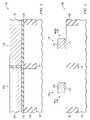
- a hard mask 112is deposited over the workpiece 102 , also shown in FIG. 1 .
- the hard mask 112preferably comprises a first layer 114 and a second layer 116 disposed over the first layer 114 , as shown.
- the hard mask 112may comprise a single layer of an oxide or a nitride material, for example.
- the first layer 114 of the hard mask 112preferably comprises about 300 Angstroms ( ⁇ ) of an oxide material such as tetraethoxysilate (TEOS), although alternatively, the first layer 114 may comprise other insulating materials deposited in other dimensions, for example.
- TEOStetraethoxysilate
- the first layer 114may be deposited by plasma-enhanced chemical vapor deposition (PECVD) or by other deposition techniques, as examples.
- the second layer 116preferably comprises about 1,500 ⁇ of a nitride material such as Si x N y , for example, although alternatively, the second layer 116 may comprise other insulating materials deposited in other dimensions, for example.
- the second layer 116may be deposited by PECVD or by other deposition techniques, as examples.
- a first layer of photoresist 118is deposited over the second layer 116 of the hard mask 112 , as shown in FIG. 1 .
- the first layer of photoresist 118may patterned with a mask using traditional lithography techniques to remove the first layer of photoresist 118 from the second region 106 of the workpiece 102 , as shown.
- the first layer of photoresist 118may be directly patterned using electron beam lithography (EBL) or other direct etching technique, as examples.
- EBLelectron beam lithography
- the first layer of photoresist 118is used to pattern at least the second layer 116 of the hard mask 112 .
- exposed portions of the second layer 116 in the second region 106may be etched using the first layer of photoresist 118 remaining over the first region 104 as a mask.
- the etch processmay be designed to stop when the first layer 114 of the hard mask 112 is reached.
- the first layer of photoresist 118is then stripped or removed, and the second layer 116 is then used as a mask to pattern the first layer 114 .
- the first layer of photoresist 118may be used as a mask to etch both the second layer 116 and the first layer 114 of the hard mask 112 , for example.
- the first layer of photoresist 118is then stripped or removed.
- a first gate dielectric material 120is deposited over the patterned hard mask 112 and exposed portions of the workpiece 102 , as shown in FIG. 2 .
- the first gate dielectric material 120preferably comprises a high-k dielectric material having a dielectric constant of about 4.0 or greater, in one embodiment.
- the first gate dielectric material 120preferably comprises HfO 2 , HfSiO X , Al 2 O 3 , ZrO 2 , ZrSiO X , Ta 2 O 5 , La 2 O 3 , SiO 2 , TiO 2 , CeO 2 , Bi 4 Si 2 O 12 , WO 3 , Y 2 O 3 , LaAlO 3 , BST (Ba (a-x) Sr x TiO 3 ), PST (PbSc x Ta (1-a) O 3 ), nitrides thereof, Si x N y , SiON, HfAlO x , HfAlO x N 1-x-y , ZrAlO x , ZrAlO x N y , SiAlO x , SiAlO x N 1-x-y , HfSiAlO x , HfSiAlO x N y , ZrSiAlO x
- the first gate dielectric material 120may comprise a single layer of material, or alternatively, the first gate dielectric material 120 may comprise two or more layers. In one embodiment, one or more of these materials can be included in the first gate dielectric material 120 in different combinations or in stacked layers.
- the first gate dielectric material 120may be deposited by chemical vapor deposition (CVD), atomic layer deposition (ALD), metal organic chemical vapor deposition (MOCVD), physical vapor deposition (PVD), or jet vapor deposition (JVD), as examples, although alternatively, the first gate dielectric material 120 may be deposited using other suitable deposition techniques.
- the first gate dielectric material 120preferably comprises a thickness of about 10 ⁇ to about 60 ⁇ in one embodiment, although alternatively, the first gate dielectric material 120 may comprise other dimensions, such as about 80 ⁇ or less, as an example.
- the first gate dielectric material 120preferably comprises a first element comprising Hf, La, Sc, Y, Lu, Lr, Ce, Pr, Nd, Pm, Sm, Eu, Gd, Tb, Dy, Ho, Er, Tm, Zr, or Yb.
- the first elementmay comprise an element from Column IIIb of the Periodic Table, or a Lanthanoid from the Periodic Table, as examples.
- the first gate dielectric material 120preferably comprises a La-containing insulating material, for example.
- the first gate dielectric material 120preferably comprises a first material such as the first element combined with a second material, such as Hf, Zr, Ta, Ti, Al, or Si, and also combined with either O, N, or both O and N.
- the first gate dielectric material 120preferably comprises a first material comprising a first element, a second material comprising Hf, Zr, Ta, Ti, Al, or Si, and also either O, N, or both O and N, and further comprising a third material, such as Ti, Sr, or Sc.
- the first gate dielectric material 120may comprise LaHfO or LaHfTiO, although alternatively, the first gate dielectric material 120 may comprise other La-containing insulating materials or first element-containing materials.
- the second transistor 138(see FIG. 6 ) to be formed in the second region 106 comprises an NMOS transistor, and if the first gate dielectric material 120 comprises La, then the La shifts the flatband voltage V FB of the NMOS transistor 138 , allowing tunability of the threshold voltage V t .
- the other types of first elements of the first gate dielectric material 120 described hereinalso are preferably adapted to tune the V t of the NMOS transistor 138 , for example.
- a first gate material 122is deposited over the first gate dielectric material 120 , also shown in FIG. 2 .
- the first gate material 122preferably comprises a conductor, such as a metal or polysilicon, although alternatively, other conductive and semiconductive materials may be used for the first gate material 122 .
- the first gate material 122preferably comprises Au, NiCu, NiTi, PtTa, RuTi, TaAlN x , TaC, TaCN, MoSi x , IrO 2 , RuO 2 , HfSi x , NbSi x , TaSi x , TiN, TiCN, HfN, TaN, W, Al, Ru, RuN, RuSiN, RuTa, TaSiN, TiSiN, TaCN, NiSi x , CoSi x , TiSi x , Ir, Y, Pt, Ti, PtTi, Pd, Re, Rh, (borides, phosphides, or antimonides of Ti), Hf, Zr, TiAlN, Mo, MoN, ZrSiN, ZrN, HfN, HfSiN, WN, Ni, Pr, VN, TiW, LaN, LaSiN, WSiN, WSi
- the gate material 122comprises FUSI
- polysiliconmay be deposited over the gate dielectric material 120 , and a metal such as nickel may be deposited over the polysilicon, although other metals may be used.
- the workpiece 102may then be heated to about 600 or 700 degrees C. to form a single layer of nickel silicide.
- the first gate material 122may comprise a plurality of stacked gate materials, such as a metal underlayer with a polysilicon cap layer disposed over the metal underlayer, or a combination of a plurality of metal layers that form a gate electrode stack.
- the first gate material 122may be deposited using CVD, PVD, ALD, or other deposition techniques, as examples.
- the first gate material 122preferably comprises a thickness of about 1,500 ⁇ , although alternatively, the first gate material 122 may comprise about 1,000 ⁇ to about 2,000 ⁇ , or other dimensions, for example.
- the first gate material 122comprises a semiconductive material
- the first gate material 122is N-doped, by doping the first gate material 122 with N type dopants such as phosphorous or antimony, for example. Doping the first gate material 122 makes the semiconductive material conductive or more conductive.
- the first gate material 122may be doped with a P type dopant, for example, as described in Ser. No. 11/017,062, filed on Dec. 20, 2004, entitled, “Transistor Device and Method of Manufacture Thereof,” which is incorporated herein by reference.
- a second layer of photoresist 124is deposited over the first gate material 122 , as shown in FIG. 2 .
- the second layer of photoresist 124may patterned using a mask using traditional lithography techniques to remove the second layer of photoresist 124 from over the first region 104 of the workpiece 102 , as shown, although alternatively, the second layer of photoresist 124 may be directly patterned.
- the second layer of photoresist 124is used as a mask to pattern the first gate material 122 and the first gate dielectric material 120 , and to remove the hard mask 112 from the first region 104 of the workpiece 102 , as shown in FIG. 3 .
- exposed portions of the first gate material 122 , first gate dielectric material 120 , and hard mask 112may be etched away from the first region 104 of the workpiece 102 using the second layer of photoresist 124 as a mask.
- the second layer of photoresist 124is then stripped or removed from over the second region 106 of the workpiece 102 .
- Any excess first gate material 122 and first gate dielectric material 120may be removed from over the optional STI region 108 using a chemical-mechanical polish (CMP) process or an etch process, for example.
- CMPchemical-mechanical polish
- the exposed surface of the workpiece 102may be cleaned using a pre-gate clean process.
- a second gate dielectric material 126is deposited over exposed portions of the workpiece 102 in the first region 104 and over the patterned first gate material 122 and first gate dielectric material 120 in the second region 106 , as shown in FIG. 4 .
- the second gate dielectric material 126preferably comprises a different material than the first gate dielectric material 120 in accordance with an embodiment of the present invention.
- the second gate dielectric material 126preferably comprises a high-k dielectric material having a dielectric constant of about 4.0 or greater, in one embodiment.
- the second gate dielectric material 126preferably comprises HfO 2 , HfSiO x , Al 2 O 3 , ZrO 2 , ZrSiO x , Ta 2 O 5 , La 2 O 3 , SiO 2 , TiO 2 , CeO 2 , Bi 4 Si 2 O 12 , WO 3 , Y 2 O 3 , LaAlO 3 , BST (Ba (a-x) Sr x TiO 3 ), PST (PbSc x Ta (1-a) O 3 ), nitrides thereof, Si x N y , SiON, HfAlO x , HfAlO x N 1-x-y , ZrAlO x , ZrAlO x N y , SiAlO x , SiAlO x N 1-x-y , HfSiAlO x , HfSiAlO x N y , ZrSiAlO
- the second gate dielectric material 126may comprise a single layer of material, or alternatively, the second gate dielectric material 126 may comprise two or more layers, wherein the top layer comprises a Fermi-pinning material. In one embodiment, one or more of these materials can be included in the second gate dielectric material 126 in different combinations or in stacked layers.
- the second gate dielectric material 126may be deposited by CVD, ALD, MOCVD, PVD, or JVD, as examples, although alternatively, the second gate dielectric material 126 may be deposited using other suitable deposition techniques.
- the second gate dielectric material 126preferably comprises a thickness of about 10 ⁇ to about 60 ⁇ in one embodiment, although alternatively, the second gate dielectric material 126 may comprise other dimensions, such as about 80 ⁇ or less, as an example. In some embodiments, the second gate dielectric material 126 preferably comprises a Fermi-pinning material such as an aluminum-containing material disposed at the top surface thereof, for example.
- the second gate dielectric material 126preferably comprises an insulating material comprising a second element, the second element being different than the first element of the first gate dielectric material 120 , for example.
- the second element in these embodimentspreferably comprises Al, Y, Sc, Lu, Lr, La, Ce, Pr, Nd, Pm, Sm, Eu, Gd, Tb, Dy, Ho, Er, Tm, Zr, or Yb, as examples.
- the second elementmay comprise an element from Column IIIb of the Periodic Table, a Lanthanoid from the Periodic table, Al or an Al-containing material, as examples.
- the first transistor 136comprises a PMOS transistor (see FIG.
- the second gate dielectric material 126preferably comprises a Y-containing insulating material or an Al-containing insulating material, for example. These materials are particularly beneficial for tuning or shifting the V FB and thus provide tunability of the V t of the PMOS transistor 136 (shown in FIG. 6 ), for example.
- the other types of second elements described hereinare also preferably adapted to provide the ability to tune the V t of the PMOS transistor 136 by varying the amount of the second element in the second gate dielectric material 126 , for example.
- the second gate dielectric material 126preferably comprises a first material such as Y or Al combined with a second material, such as Hf, Zr, Ta, Ti, Al, or Si, and also combined with either O, N, or both O and N, as example, as another example.
- the second gate dielectric material 126preferably comprises a first material comprising Y or Al, a second material comprising Hf, Zr, Ta, Ti, Al, or Si, and also either O, N, or both O and N, and further comprising a third material, such as Ti, Sr, or Sc.
- the second gate dielectric material 126may comprise YHfO, YHfTiO, or AlO, although alternatively, the second gate dielectric material 126 may comprise other materials.
- the second gate material 128is deposited over the second gate dielectric material 126 , also shown in FIG. 4 .
- the second gate material 128preferably comprises a conductor, such as a metal or polysilicon, although alternatively, other conductive and semiconductive materials may be used for the second gate material 128 .
- the second gate material 128preferably comprises Au, NiCu, NiTi, PtTa, RuTi, TaAlN x , TaC, TaCN, MoSi x , IrO 2 , RuO 2 , HfSi x , NbSi x , TaSi x , TiN, TiCN, HfN, TaN, W, Al, Ru, RuN, RuSiN, RuTa, TaSiN, TiSiN, TaCN, NiSi x , CoSi x , TiSi x , Ir, Y, Pt, Ti, PtTi, Pd, Re, Rh, (borides, phosphides, or antimonides of Ti), Hf, Zr, TiAlN, Mo, MoN, ZrSiN, ZrN, HfN, HfSiN, WN, Ni, Pr, VN, TiW, LaN, LaSiN, WSiN, WSi, poly
- the second gate material 128may comprise a plurality of stacked gate materials, such as a metal underlayer with a polysilicon cap layer disposed over the metal underlayer, or a combination of a plurality of metal layers that form a gate electrode stack.
- the second gate material 128may be deposited using CVD, PVD, ALD, or other deposition techniques, as examples.
- the second gate material 128preferably comprises a thickness of about 1,500 ⁇ , although alternatively, the second gate material 128 may comprise about 1,000 ⁇ to about 2,000 ⁇ , or other dimensions, for example.
- the second gate material 128may comprise the same material as the first gate material 122 , or alternatively, the second gate material 128 may comprise a different material than the first gate material 122 , for example.
- the second gate material 128comprises a semiconductive material
- the second gate material 128is P-doped, by doping the second material 128 with a P type dopant such as boron, as an example. Doping the second gate material 128 makes the semiconductive material conductive or more conductive.
- the second gate material 128is preferably doped with an N type dopant, for example.
- the second gate material 128may be doped with the same dopant type or a different dopant type than the first gate material 122 is doped with, for example.
- a third layer of photoresist 130is deposited over the second gate material 128 , as shown in FIG. 4 .
- the third layer of photoresist 130may be patterned using a mask by traditional lithography techniques to remove the third layer of photoresist 130 from the second region 106 of the workpiece 102 , as shown, although alternatively, the third layer of photoresist 130 may be directly patterned.
- the third layer of photoresist 130is then used as a mask to pattern the second gate material 128 and second gate dielectric material 126 , as shown in FIG. 5 .
- exposed portions of the second gate material 128 and second gate dielectric material 126may be etched away from the second region 106 of the workpiece 102 using the third layer of photoresist 130 as a mask.
- the third layer of photoresist 130is then stripped or removed from over the first region 104 of the workpiece 102 .
- Any excess second gate material 128 and second gate dielectric material 126may be removed from over the optional STI region 108 proximate the interface of the first region 104 and second region 106 using a chemical-mechanical polish (CMP) process or an etch process, for example (not shown), leaving the structure shown in FIG. 5 .
- CMPchemical-mechanical polish
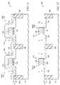
- the first gate material 120 , the first gate dielectric material 122 , the second gate material 126 , and the second gate dielectric material 128are simultaneously patterned with a desired pattern for a CMOS device, leaving the structure shown in FIG. 6 , wherein a PMOS transistor 136 is formed in the first region 104 , and an NMOS transistor 138 is formed in the second region 106 .
- the gate dielectric of the PMOS transistor 136comprises the second gate dielectric material 126
- the gate dielectric of the NMOS transistor 138comprises the first gate dielectric material 120 .
- the gate or gate electrode of the PMOS transistor 136comprises the second gate material 128
- the gate of the NMOS transistor 138comprises the first gate material 122
- the gate dielectric 126 of the PMOS transistor 136preferably comprises an insulating material that is different than the insulating material of the gate dielectric 120 of the NMOS transistor 138 .
- CMOS Transistor With Dual High-k Gate Dielectric and Method of Manufacture Thereofwhich is incorporated herein by reference.
- a first insulating layermay be deposited over the entire workpiece, (not shown in the drawings), and the first insulating layer may be removed in one region, such as first region 104 , but not the other region, such as second region 106 .
- a second insulating layermay then be deposited over the first insulating layer in the second region 106 and over the workpiece 102 in the first region 104 . Then a single layer of gate material is formed over the second insulating layer. The gate material and insulating layers are then patterned to form a PMOS transistor having a gate dielectric comprising the second insulating layer, and an NMOS transistor having a gate dielectric comprising both the first and second insulating layers.
- a single layer of insulating materialmay be deposited over the workpiece 102 , and a gate material comprising a conductive material, for example, may be deposited over the insulating material (also not shown).
- One region, such as the first region 104may be masked, while the other region, such as second region 106 , is implanted with a Fermi-pinning material.
- the gate materialmay be implanted with the Fermi-pinning material.
- the insulating materialis also implanted with the Fermi-pinning material, for example.
- the gate material of the PMOS transistormay be implanted with a different material than the gate material of the NMOS transistor is implanted with, for example.
- the workpiece 102is recessed in the source and drain regions, as shown in FIG. 7 .
- the source regions and drain regionse.g., source region S 1 and drain region D 1 of the PMOS transistor 136 , and source region S 2 and drain region D 2 of the NMOS transistor 138
- the etch processin one embodiment is preferably substantially anisotropic, to avoid reducing the horizontal dimensions (e.g., lateral etching) of the gates 128 and 122 and the gate dielectric 126 and 120 , for example.
- the etch process to create the recessesmay comprise an isotropic etch, such as an etch process referred to as “chemical downstream etching,” which is a technique employing microwave plasma source, low bias RF power, or a combination of both, for isotropic recessing of silicon in the workpiece 102 selective to the isolation oxide 108 , as an example, although other isotropic etch processes may alternatively be used.
- the depth d 1 of the recesses in the source S 1 /S 2 and drain D 1 /D 2 regionspreferably comprises about 200 ⁇ or less below the top surface of the workpiece 102 , as an example.
- the source S 1 /S 2 regions and the drain D 1 /D 2 regionsare recessed simultaneously in a single processing step, e.g., they are recessed at the same time.
- the source S 1 /S 2 regions and drain D 1 /D 2 regionsmay be recessed using an additional separate etch process, or alternatively, the source S 1 /S 2 regions and the drain D 1 /D 2 regions may be recessed during the gate 128 / 122 and gate dielectric 126 / 120 patterning process, for example.
- Two recessesare preferably formed for each transistor 136 and 138 , as shown.
- a first recessis formed in the workpiece 102 on a first side of the gate dielectric 126 proximate the gate dielectric 126
- a second recessis formed in the workpiece 102 on a second side of the gate dielectric 126 proximate the gate dielectric 126 , for example, opposite from the first side of the gate dielectric 126 .
- a third recessis formed in the workpiece 102 on a first side of the gate dielectric 120 proximate the gate dielectric 120
- a fourth recessis formed in the workpiece 102 on a second side of the gate dielectric 120 proximate the gate dielectric 120 , for example, opposite from the first side of the gate dielectric 120 , as shown.
- the recesses in the workpiece 102 of the PMOS transistor 136are filled with a first dopant-bearing metal while the NMOS transistor 138 is masked, and then the recesses in the workpiece 102 of the NMOS transistor 138 are filled with a second dopant bearing metal, to be described next with reference to FIGS. 8 through 10 .
- a masking material 139 athat may comprise a hard mask including about 5,000 ⁇ of an oxide, a nitride, or combinations thereof, as examples, is deposited over the first region 104 and the second region 106 of the workpiece 102 , and then the masking material 139 a is removed from over the first region 104 , e.g., using lithography, as shown in FIG. 8 .
- a first dopant-bearing metal 140is deposited over exposed portions of the workpiece 102 , the top surface of the gate 128 , and isolation regions 108 , in the first region 104 , and over the masking material 139 a in the second region 106 , as shown in FIG. 8 .
- the first dopant-bearing metal 140preferably comprises a metal that includes a first dopant comprising boron (B), phosphorous (P), arsenic (As), or antimony (Sb), as examples, although alternatively, the dopant may comprise other dopant materials.
- the transistor 136 in the first region 104comprises a PMOS transistor, for example, preferably the workpiece 102 is lightly doped with an N type material in the first region 104 , and the first dopant preferably comprises a P type material, for example.
- the first dopant-bearing metal 140preferably comprises TiB 2 , ZrB 2 , HfB 2 , ZrP, TiP, ZrSb 2 , TiSb 2 , HfSb 2 , or arsinides of Zr or Hf, as examples, although alternatively, the dopant-bearing metal 140 may comprise other metals containing a first dopant.
- the first dopant-bearing metal 140preferably comprises Au, NiCu, NiTi, PtTa, RuTi, TaAlN x , TaC, TaCN, MoSi x , IrO 2 , RuO 2 , HfSi x , NbSi x , TaSi x , TiN, TiCN, HfN, TaN, W, Al, Ru, RuN, RuSiN, RuTa, TaSiN, TiSiN, TaCN, NiSi x , CoSi x , TiSi x , Ir, Y, Pt, Ti, PtTi, Pd, Re, Rh, (borides, phosphides, or antimonides of Ti), Hf, Zr, TiAlN, Mo, MoN, ZrSiN, ZrN, HfN, HfSiN, WN, Ni, Pr, VN, TiW, LaN, LaSi
- the metal portion (e.g., Ti, Zr, Hf, or other materials listed) of the first dopant-bearing metal 140causes the source S 1 and drain D 1 regions to have a lower sheet resistance R s , and the first dopant portion (e.g., B, P, Sb, As) creates the junction of the source S 1 and drain D 1 .
- the first dopant-bearing metal 140is selected to provide a reduced sheet resistance R s for the semiconductor device 100 .
- the recesses in the source S 1 and drain D 1 regionsare preferably back-filled with the first dopant-bearing metal 140 .
- the first dopant-bearing metal 140may be deposited using electron beam evaporation, CVD, or PVD, although alternatively, other methods of deposition may be used to deposit the first dopant-bearing metal 140 .
- the first dopant-bearing metal 140may be substantially conformal when deposited, as shown in FIG. 8 . Excess portions of the first dopant-bearing metal 140 are removed from over the isolation regions 108 , top surface and sidewalls of the gates 128 , and sidewalls of the gate dielectric 126 , as shown in FIG. 9 . The excess portions of the first dopant-bearing metal 140 may be removed using an anisotropic etch process or an isotropic etch process, as examples. As examples, the excess portions of the first dopant-bearing metal 140 may be removed using wet, dry, electrochemical or chemical etch processes, although other etch processes may alternatively be used.
- the top surface of the first dopant-bearing metal regions 140 formed in the source S 1 and drain D 1 regionsmay be substantially planar with the top surface of the workpiece 102 , as shown in FIG. 9 , although alternatively, the first dopant-bearing metal regions 140 may be slightly recessed or concaved slightly within the recesses of the workpiece 102 (not shown).
- the masking material 139 ais removed from the second region 106 of the workpiece 102 .
- a second masking material 139 bcomprising similar materials and thicknesses as described for the masking material 139 a is formed or deposited over the first region 104 and the second region 106 of the workpiece 102 .
- the masking material 139 bis removed from over the second region 106 , as shown in FIG. 9 , leaving the gate material 122 and portions of the workpiece 102 exposed.
- a second dopant-bearing metal 141is deposited over the exposed portions of the workpiece 102 , top surface and sidewalls of the gate material 122 , and sidewalls of the gate dielectric 120 in the second region 106 , and also over the masking material 139 b in the first region, as shown in FIG. 9 .
- the second dopant-bearing metal 141preferably comprises similar materials and dimensions as described for the first dopant-bearing metal 140 , for example.
- the second dopant-bearing metal 141preferably comprises a different material than the first dopant-bearing metal 140 , for example.
- the second dopant-bearing metal 141preferably comprises a second dopant, wherein the second dopant is different than the first dopant of the first dopant-bearing metal 140 , for example.
- the transistor 138 in the second region 106comprises an NMOS transistor
- the workpiece 102is preferably lightly doped with a P type dopant in the second region 106
- the second dopant-bearing metal 141preferably comprises an N type material, for example.
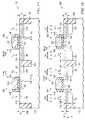
- Excess portions of the second dopant-bearing metal 141are removed from over the isolation regions 108 in the second region 106 , top surface and sidewalls of the gates 122 , and sidewalls of the gate dielectric 120 , using the methods described for the first dopant-bearing metal 140 , and leaving the structure shown in FIG. 10 , wherein the first dopant-bearing metal 140 fills the recesses in the workpiece 102 in the first region 104 , and wherein the second dopant-bearing metal 141 fills the recesses in the workpiece 102 in the second region 106 .
- the top surface of the second dopant-bearing metal regions 141 formed in the source S 2 and drain D 2 regionsmay be substantially planar with the top surface of the workpiece 102 , as shown in FIG. 10 , although alternatively, the second dopant-bearing metal regions 141 may be slightly recessed or concaved slightly within the recesses of the workpiece 102 (not shown).
- the masking material 139 b shown in FIG. 9is removed from the first region 106 of the workpiece 102 , as shown in FIG. 10 .
- a single metal layer 143is deposited over the first region 104 and the second region 106 of the workpiece 102 , as shown in FIG. 11 .
- the metal layer 143may be masked in the second region 106 while a first dopant is implanted into the metal layer 143 in the first region 104
- the metal layer 143may be masked in the first region 104 while a second dopant is implanted into the metal layer 143 in the second region 106 . Excess portions of the metal layer 143 are then removed from above a top surface of the workpiece 102 , leaving the structure shown in FIG.
- the metal layer 143 implanted with the first dopantcomprises a first dopant-bearing metal 140 in the first region 104 and the metal layer 143 implanted with the second dopant comprises a second dopant-bearing metal 141 in the second region 106 .
- the gates 128 and 122are not implanted with the first dopant and second dopant, respectively, in this embodiment, so that the gate 128 may be doped with a different type dopant than the first dopant-bearing metal 140 , and the gate 122 may be doped with a different type dopant than the second dopant-bearing metal 141 , for example.
- excess portions of the metal layer 143are removed from above the top surface of the workpiece 102 , leaving the structure shown in FIG. 12 .
- the metal layer 143is masked in the second region 106 while a first dopant 145 is implanted into the metal layer 143 in the first region 104 , forming a first dopant-bearing metal 140 as shown in FIG. 13 .
- the gate 128 in the first region 104is also implanted with the first dopant 145 in this embodiment.
- the metal layer 143may be masked in the first region 104 while a second dopant 147 is implanted into the metal layer 143 in the second region 106 , forming a second dopant-bearing metal 141 as shown in FIG. 13 .
- the gate 122 in the second region 106is also implanted with the second dopant 147 in this embodiment.
- the first and second dopant-bearing metal regions 140 and 141may be doped using an additional ion implantation step (e.g., masking one region 104 while implanting the other region 106 ), not shown.
- an additional ion implantation stepe.g., masking one region 104 while implanting the other region 106 .
- dopant ionsare introduced into the dopant-bearing metal regions 140 and 141 using ion implantation.
- the implantationis performed at an energy level of about 1 KeV or below at an implantation dose of about 1 ⁇ 10 15 ions/cm 2 or less, as examples.
- the workpiece 102is then subjected to a low-temperature anneal process to cause out-diffusion of the first and second dopants in the dopant-bearing metal regions 140 and 141 , respectively.
- the out-diffusion of the first dopant in the first region 104forms a doped region 144 comprising the first dopant in the source S 1 region and drain D 1 region within the workpiece 102 adjacent the dopant-bearing metal regions 140 , as shown in FIG. 14 .
- the anneal processalso causes out-diffusion of the second dopant in the second region 106 , forming a doped region 149 comprising the second dopant in the source S 2 region and drain D 2 region within the workpiece 102 adjacent the dopant-bearing metal regions 141 .
- the doped regions 144 and 149preferably extend beneath the dopant-bearing metal regions 140 and 141 , and also extend laterally (to the side of the dopant-bearing metal regions 140 and 141 ) beneath the gates 128 / 122 and gate dielectric 126 / 120 by about 70 ⁇ or less, as shown at d 2 .
- the low-temperature anneal processpreferably comprises a temperature of about 900° C. or less for about 1 hour or less, and more preferably comprises a temperature of about 900° C. for about 20 minutes or less, as examples.
- the doped regions 144preferably comprise a thickness of about 100 ⁇ or less, as an example.
- the source S 1 /S 2 and the drain D 1 /D 2 regionseach comprise a dopant-bearing metal 140 / 141 and a doped region 144 / 149 disposed adjacent (e.g., below and extending laterally from) the dopant-bearing metal 140 / 141 , as shown.
- the source S 1 /S 2 and drain D 1 /D 2 regionspreferably comprise a total thickness d 3 of about 300 ⁇ below the top surface of the workpiece 102 , comprising the dopant-bearing metal 140 / 141 and the doped regions 144 / 149 .
- the doped regions 144 / 149include an extension region that extends beneath the gate dielectric 126 / 120 and extends towards the channel regions C 1 and C 2 .
- One advantage of the transistors 136 and 138 formed in accordance with embodiments of the present inventionis that the extension region can be made smaller than in traditional transistor designs.
- the extension regionmay extend beneath the gates 128 / 122 on either side by a distance d 2 , which may comprise about 70 ⁇ or less, e.g., about 20 to about 50 ⁇ . This is advantageous because the resistance of the extension region is low, resulting from the reduced amount of overlap d 2 , which reduces hot carrier effects of the transistors 136 and 138 .
- the dopant-bearing metal 140 / 141preferably comprises a higher atomic percentage of the dopant than would be found in a natural state of the dopant-bearing metal 140 / 141 , and the percentage of the dopant in the dopant-bearing metal 140 / 141 is reduced after the low-temperature anneal, resulting from dopant ions diffusing into the workpiece 102 to form the doped regions 144 / 149 .
- the dopant-bearing metal 140 in the first region 104comprises Ti bearing the dopant B
- the dopant-bearing metal 140may comprise TiB x , where x>2, e.g., 3, 4, etc.
- the dopant-bearing metal 140comprises a reduced atomic percentage of the first dopant, and may comprise, for example, TiB 2 . Note that while there is less of the dopant species (e.g., the first dopant) left residing in the dopant-bearing metal 140 after the low-temperature anneal because some dopant atoms migrate to the dopant region 144 , some dopant species are still left residing in the dopant-bearing metal 140 .
- the dopant speciese.g., the first dopant
- the manufacturing process for the device 100is then continued to complete the device 100 , preferably without subjecting the semiconductor device 100 to high temperatures, e.g., preferably without exposing the semiconductor device 100 to a temperature greater than about 900° C.
- a spacer material 146comprising a dielectric material such as SiO 2 , SiN, or SiON, as examples, although other insulating materials may also be used, may be deposited over exposed portions of the workpiece 102 .
- the sidewall spacer 146 materialmay be exposed to an etch process such as an anisotropic etch to form sidewall spacers 146 on the transistors 136 and 138 in the first and second regions 104 and 106 of the workpiece 102 , as shown in FIG. 15 .
- transistors 136 and 138are formed that include gates 128 / 122 , source regions S 1 /S 2 , and drain regions D 1 /D 2 , wherein the source S 1 /S 2 and drain D 1 /D 2 comprise the dopant-bearing metal regions 140 / 141 and the doped regions 144 / 149 .
- the transistors 136 and 138have a thin effective oxide thickness which includes the gate dielectric 126 / 120 and in some embodiments also includes a thin interface region disposed between the workpiece 102 and the gate dielectric 126 / 120 (not shown).
- the thin interface regionmay form during the deposition process of the gate dielectric materials 126 and 120 , for example, and may comprise a thin oxide layer, for example.
- a high-temperature anneal processe.g., at temperatures of about 1,000° C. or more, increasing the thickness of the interface region, if present, is avoided, thus decreasing the effective oxide thickness of the transistors 136 and 138 .
- a low-temperature anneal processis preferably used to form the doped regions 144 / 149 of the source S 1 /S 2 and drain D 1 /D 2 regions, this results in a shallower junction depth (e.g., depth d 3 of the source and drain regions S 1 /S 2 and D 1 /D 2 ) of the transistors 136 and 138 .
- the transistors 136 and 138are particularly advantageous in applications wherein a high drive current and minimal effective oxide thickness are important, such as in high performance (e.g., high speed) applications, for example, in use with memory and other devices.
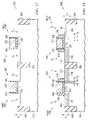
- FIG. 16shows an embodiment of the present invention, in which a similar process flow may be used as was described for FIGS. 1 through 15 .
- an ion implantation process 150 and 151is used to implant a dopant into the first and second regions 104 and 106 , respectively (e.g., while the other region not being implanted is covered by a mask), followed by a high temperature anneal process, at a temperature of about 1,000° C.
- the target depth of this optional ion implantation processis preferably greater than the depth of the dopant bearing metal 140 and doped region 144 , in one embodiment, as an example.
- the deep source and drain implantation regions 152 / 153may comprise a depth d 4 of about 500 ⁇ or greater beneath the workpiece 102 top surface, for example.
- the PMOS transistor 136may be implanted with a dopant 150 comprising BF 2
- the NMOS transistor 138may be implanted with a dopant 151 comprising As, as examples, at an energy level of about 10 KeV at an implantation dosage of about 1 ⁇ 10 5 ions/cm 2 , as examples.
- the dopant 150preferably comprises the same dopant type as the first dopant of the first dopant-bearing metal 140
- the dopant 151preferably comprises the same dopant type as the second dopant of the second dopant-bearing metal 141 , as example.
- the resulting transistors 136 and 138may have a thicker interface region (not shown) than the interface region of the transistors 136 and 138 in FIG. 15 , and may also have an additional interface region comprising an oxide formed between the gate dielectrics 126 / 120 and the gates 128 / 120 (also not shown), yet the transistors 136 and 138 in FIG. 16 benefit from a further reduction in sheet resistance R s due to the presence of the dopant-bearing metal 140 and 141 of the source S 1 /S 2 and drain D 1 /D 2 .
- This CMOS device 100is advantageous in some transistor applications that require a deeper source S 1 /S 2 and drain D 1 /D 2 implantation process to prevent junction leakage current from the source S 1 /S 2 and drain D 1 /D 2 to the workpiece 102 , such as in low power applications. In these applications, a higher effective oxide thickness does not deleteriously affect the transistor 136 and 138 performance, for example.
- FIGS. 17 through 19show additional preferred embodiments of the present invention, in which a double spacer 260 / 246 is used adjacent the gate dielectric and gate, along the sidewalls.
- a similar process flow and structuremay be used as was described for FIGS. 1 through 15 and 16 for the embodiments shown in FIGS. 17 through 18 and 19 .
- Similar reference numbersare designated for the various elements in FIGS. 17 through 18 and 19 as were used in FIGS. 1 through 11 and 12 . To avoid repetition, each reference number shown in FIGS. 17 through 18 and 19 is not described in detail herein. Rather, similar materials and thicknesses described for x02, x04, etc. . . . are preferably used for the material layers shown as were described for FIGS.
- the preferred and alternative materials listed for the dopant-bearing metal 140 in the description for FIGS. 1 through 11 and 12are preferably also used for the dopant-bearing metal 240 in FIG. 18 .
- FIGS. 17 through 18show cross-sectional views of a preferred embodiment of the present invention, wherein a first spacer 260 is formed over the sidewalls of the gates 228 / 222 and gate dielectrics 226 / 220 before forming the recesses in the source S 1 /S 2 and drain D 1 /D 2 regions.
- the first spacers 260preferably comprise a thickness of about 50 ⁇ or less, and may comprise an insulating material such as SiO 2 , SiN, or SiON, as examples. Similar manufacturing processes and materials are used as were described for the embodiment shown in FIGS. 7 through 15 , resulting in the formation of transistors 236 and 238 shown in FIG. 18 in a cross-sectional view.
- a second spacer 246is formed adjacent and abutting the first spacers 260 , as shown in FIG. 18 , after the formation of the source S 1 /S 2 and drain D 1 /D 2 regions as described herein.
- the transistors 236 and 238have a decreased effective oxide thickness of the gate dielectrics 226 / 220 , and have a junction depth d 3 that is well-controlled and very shallow.
- This embodimentis advantageous in that the extension regions d 5 of the source S 1 /S 2 and drain D 1 /D 2 regions are further reduced, extending a distance d 5 of about 50 ⁇ or less beneath the edge of the gates 228 / 222 and gate dielectrics 226 / 220 , as shown.
- the low temperature anneal processresults in the formation of the doped regions 244 and 249 that extend less beneath the gates 228 / 222 and gate dielectrics 226 / 220 due to the presence of the spacer 260 on the sidewalls of the gates 228 / 222 and gate dielectrics 226 / 220 .
- the amount that the extension is reducedis substantially the width of the spacer 260 , or the dimension d 6 of the thickness of the doped regions 244 and 249 less dimension d 5 of the amount that the doped regions 244 and 249 extend beneath the gates 228 / 222 and gate dielectrics 226 / 220 , for example.
- FIG. 19shows an embodiment of the present invention, wherein a first spacer 260 and second spacer 246 are used, as described for FIGS. 17 and 18 .
- the workpiece 202is subjected to a subsequent ion implantation process to form deep source and drain implantation regions 252 / 253 in the source S 1 /S 2 and drain D 1 /D 2 , as described with reference to the embodiment shown in FIG. 16 .
- FIG. 19shows an embodiment of the present invention, wherein a first spacer 260 and second spacer 246 are used, as described for FIGS. 17 and 18 .
- the workpiece 202is subjected to a subsequent ion implantation process to form deep source and drain implantation regions 252 / 253 in the source S 1 /S 2 and drain D 1 /D 2 , as described with reference
- the relatively high anneal temperatures required to form the deep source and drain implantation regions 252 / 253result in an increased EOT, but this does not present a problem in some applications.
- the transistors 236 and 238have a decreased sheet resistance R s .
- a thin layer of silicon 370may be formed between the gate dielectric 320 and 326 and the gate 322 and 328 of the transistors 338 and 336 in accordance with embodiments of the present invention, as described in U.S. patent application Ser. No. 11/005,292, filed on Dec. 6, 2004, entitled, “CMOS Transistor and Method of Manufacture Thereof,” which is incorporated herein by reference.
- a thin layer of silicon 370is formed over the gate dielectric materials 320 and 326 , before depositing the gate materials 322 and 328 , respectively.
- the thin layer of silicon 370may provide pinning of the work function of the PMOS transistor 336 and the NMOS transistor 338 , for example.
- dopants 480 and 482may be implanted into the gates 428 and 422 of the transistors 436 and 438 , as shown in FIG. 21 .
- the dopants 480 and 482may comprise the same dopant species or different dopant species, for example.
- the PMOS transistor 436 gatemay be implanted with an N type dopant
- the NMOS transistor 438 gatemay be implanted with a P or N type dopant, as described in Ser. No. 11/017,062, filed on Dec. 20, 2004, entitled, “Transistor Device and Method of Manufacture Thereof,” which is incorporated herein by reference.
- An advantage of these embodimentsis the reduction of a “poly depletion” effect that can occur when polysilicon is used as a gate electrode material.
- a poly depletion effectcan increase the inversion oxide thickness (T inv ) (or capacitance equivalent thickness (CET)) of a transistor by about 4 ⁇ , for example, which results in decreasing the device performance significantly, e.g., by about 20%.
- N type dopant in PMOS transistorscan eliminate a boron penetration effect (e.g., which can occur when a polysilicon gate electrode is implanted with boron, because boron diffuses from the gate and into the gate dielectric and/or channel region of the workpiece), which can deteriorate the gate dielectric quality and also increase the off-state leakage current.
- using polysilicon as a gate electrode materialis an advantage, because manufacturing processes using polysilicon materials are mature, making these embodiments more manufacturing-friendly and easily integratable into production processes.
- the PMOS transistor 436 gatemay be implanted with a P type dopant, and the NMOS transistor 438 may be implanted with an N type dopant, for example.
- the first region 404 of the workpiece 402may be masked (not shown) while the second region 406 is implanted with the dopant 482 , and vice versa, for example.
- CMOS devicesand methods of manufacturing thereof.
- the work functions of the CMOS transistors described hereinare tunable by a wide variety of factors, such as the gate dielectric material, gate material, doping, and optional thin layer of silicon.
- the junction depth X je.g., of the source and drain regions S 1 /S 2 and D 1 /D 2 ) is reduced, and the effective oxide thickness is reduced, of the novel transistors and CMOS devices described herein.
- Embodiments of the present inventionprovide novel CMOS device structures and methods of manufacture thereof that combine a “dual high-k” structure wherein the PMOS gate dielectric and NMOS gate dielectric comprise different materials, with a “metal junction” structure wherein the source and drain regions comprise a dopant-bearing metal.
- Advantages of embodiments of the present inventioninclude providing improved EOT scaling because of the lower thermal budget of the metal junction formation process than in traditional implant-anneal junction processes (e.g., used to form source and drain regions). Because of the lower thermal budget, high temperature anneal processes are not required to form the source and drain regions of the transistors, and more band-edge metal gate materials may be used. For example, the work function of metals is a function of the process temperature.
- band-edge work functions at a low temperaturee.g., less than about 900° C.
- a high temperature source/drain activation anneale.g., of greater than about 900° C.
- band-edge metalsBy lowering the thermal process temperature by the use of the novel embodiments of the present invention described herein, there are more choices of the metals that can be used in production, e.g., for the gate electrode and source and drain region materials.
- the drive current of the transistorsis increased (and hence, the circuit speed is increased), the short channel effect is reduced, and junction leakage current is also reduced, as examples.
Landscapes
- Engineering & Computer Science (AREA)
- Physics & Mathematics (AREA)
- Condensed Matter Physics & Semiconductors (AREA)
- General Physics & Mathematics (AREA)
- Manufacturing & Machinery (AREA)
- Computer Hardware Design (AREA)
- Microelectronics & Electronic Packaging (AREA)
- Power Engineering (AREA)
- Metal-Oxide And Bipolar Metal-Oxide Semiconductor Integrated Circuits (AREA)
- Insulated Gate Type Field-Effect Transistor (AREA)
Abstract
Description
Claims (16)
Priority Applications (3)
| Application Number | Priority Date | Filing Date | Title |
|---|---|---|---|
| US11/305,567US7510943B2 (en) | 2005-12-16 | 2005-12-16 | Semiconductor devices and methods of manufacture thereof |
| DE102006059014ADE102006059014B4 (en) | 2005-12-16 | 2006-12-14 | Method for producing a semiconductor device |
| US12/395,743US8004047B2 (en) | 2005-12-16 | 2009-03-02 | Semiconductor devices and methods of manufacture thereof |
Applications Claiming Priority (1)
| Application Number | Priority Date | Filing Date | Title |
|---|---|---|---|
| US11/305,567US7510943B2 (en) | 2005-12-16 | 2005-12-16 | Semiconductor devices and methods of manufacture thereof |
Related Child Applications (1)
| Application Number | Title | Priority Date | Filing Date |
|---|---|---|---|
| US12/395,743DivisionUS8004047B2 (en) | 2005-12-16 | 2009-03-02 | Semiconductor devices and methods of manufacture thereof |
Publications (2)
| Publication Number | Publication Date |
|---|---|
| US20070141797A1 US20070141797A1 (en) | 2007-06-21 |
| US7510943B2true US7510943B2 (en) | 2009-03-31 |
Family
ID=38170086
Family Applications (2)
| Application Number | Title | Priority Date | Filing Date |
|---|---|---|---|
| US11/305,567Expired - Fee RelatedUS7510943B2 (en) | 2005-12-16 | 2005-12-16 | Semiconductor devices and methods of manufacture thereof |
| US12/395,743Expired - Fee RelatedUS8004047B2 (en) | 2005-12-16 | 2009-03-02 | Semiconductor devices and methods of manufacture thereof |
Family Applications After (1)
| Application Number | Title | Priority Date | Filing Date |
|---|---|---|---|
| US12/395,743Expired - Fee RelatedUS8004047B2 (en) | 2005-12-16 | 2009-03-02 | Semiconductor devices and methods of manufacture thereof |
Country Status (2)
| Country | Link |
|---|---|
| US (2) | US7510943B2 (en) |
| DE (1) | DE102006059014B4 (en) |
Cited By (9)
| Publication number | Priority date | Publication date | Assignee | Title |
|---|---|---|---|---|
| US20060154511A1 (en)* | 2004-12-14 | 2006-07-13 | Sumitomo Wiring Systems, Ltd. | Connector |
| US20080194087A1 (en)* | 2007-02-12 | 2008-08-14 | Chen-Hua Yu | Polysilicon gate formation by in-situ doping |
| US20080194072A1 (en)* | 2007-02-12 | 2008-08-14 | Chen-Hua Yu | Polysilicon gate formation by in-situ doping |
| US20090159991A1 (en)* | 2007-12-20 | 2009-06-25 | Bernd Ernst Eduard Kastenmeier | Cmos devices with different metals in gate electrodes using spin on low-k material as hard mask |
| US20100068873A1 (en)* | 2008-09-16 | 2010-03-18 | Jing-Cheng Lin | Depletion-Free MOS using Atomic-Layer Doping |
| CN102280376A (en)* | 2010-06-08 | 2011-12-14 | 中国科学院微电子研究所 | Method for integrating double metal gate double high dielectric for CMOS device |
| US20130069166A1 (en)* | 2011-09-15 | 2013-03-21 | Yun-Hyuck Ji | Method for fabricating semiconductor device |
| US20130230952A1 (en)* | 2012-03-01 | 2013-09-05 | Taiwan Semiconductor Manufacturing Company, Ltd. | Integrated circuit device and method of manufacturing same |
| CN110911352A (en)* | 2019-12-04 | 2020-03-24 | 西安文理学院 | Diffusion barrier layer for Cu interconnection and preparation method and application thereof |
Families Citing this family (19)
| Publication number | Priority date | Publication date | Assignee | Title |
|---|---|---|---|---|
| US20040036129A1 (en)* | 2002-08-22 | 2004-02-26 | Micron Technology, Inc. | Atomic layer deposition of CMOS gates with variable work functions |
| US20070164323A1 (en)* | 2006-01-18 | 2007-07-19 | Micron Technology, Inc. | CMOS gates with intermetallic compound tunable work functions |
| US7709402B2 (en) | 2006-02-16 | 2010-05-04 | Micron Technology, Inc. | Conductive layers for hafnium silicon oxynitride films |
| KR20070102927A (en)* | 2006-04-17 | 2007-10-22 | 마쯔시다덴기산교 가부시키가이샤 | Solid state imaging device and manufacturing method thereof |
| US20090053883A1 (en)* | 2007-08-24 | 2009-02-26 | Texas Instruments Incorporated | Method of setting a work function of a fully silicided semiconductor device, and related device |
| US20090108294A1 (en)* | 2007-10-30 | 2009-04-30 | International Business Machines Corporation | Scalable high-k dielectric gate stack |
| US20090152651A1 (en)* | 2007-12-18 | 2009-06-18 | International Business Machines Corporation | Gate stack structure with oxygen gettering layer |
| US7622341B2 (en)* | 2008-01-16 | 2009-11-24 | International Business Machines Corporation | Sige channel epitaxial development for high-k PFET manufacturability |
| US8114727B2 (en)* | 2008-08-29 | 2012-02-14 | Texas Instruments Incorporated | Disposable spacer integration with stress memorization technique and silicon-germanium |
| US8592325B2 (en)* | 2010-01-11 | 2013-11-26 | International Business Machines Corporation | Insulating layers on different semiconductor materials |
| US8421132B2 (en)* | 2011-05-09 | 2013-04-16 | International Business Machines Corporation | Post-planarization UV curing of stress inducing layers in replacement gate transistor fabrication |
| US8822292B2 (en) | 2011-11-23 | 2014-09-02 | Institute of Microelectronics, Chinese Academy of Sciences | Method for forming and controlling molecular level SiO2 interface layer |
| CN103137460B (en)* | 2011-11-23 | 2016-02-10 | 中国科学院微电子研究所 | Molecular scale interface SiO2Forming and controlling method |
| US8987080B2 (en)* | 2012-04-26 | 2015-03-24 | Applied Materials, Inc. | Methods for manufacturing metal gates |
| JP2014072388A (en)* | 2012-09-28 | 2014-04-21 | Fujitsu Ltd | Compound semiconductor device and manufacturing method of the same |
| US9768254B2 (en)* | 2015-07-30 | 2017-09-19 | International Business Machines Corporation | Leakage-free implantation-free ETSOI transistors |
| CN106893919A (en)* | 2017-02-23 | 2017-06-27 | 宁波高新区远创科技有限公司 | A kind of preparation method of the lightning protection alloy of resistance to ablation |
| WO2019182959A1 (en)* | 2018-03-20 | 2019-09-26 | Tokyo Electron Limited | Platform and method of operating for integrated end-to-end gate contact process |
| US12336264B2 (en)* | 2022-06-21 | 2025-06-17 | Nanya Technology Corporation | Semiconductor device having gate electrodes with dopant of different conductive types |
Citations (97)
| Publication number | Priority date | Publication date | Assignee | Title |
|---|---|---|---|---|
| US4432035A (en) | 1982-06-11 | 1984-02-14 | International Business Machines Corp. | Method of making high dielectric constant insulators and capacitors using same |
| US4990974A (en) | 1989-03-02 | 1991-02-05 | Thunderbird Technologies, Inc. | Fermi threshold field effect transistor |
| US5041885A (en) | 1989-05-02 | 1991-08-20 | Sgs-Thomson Microelectronics S.R.L. | Surface field effect transistor with depressed source and/or drain areas for ULSI integrated devices |
| US5066995A (en) | 1987-03-13 | 1991-11-19 | Harris Corporation | Double level conductor structure |
| US5162263A (en) | 1989-11-27 | 1992-11-10 | Kabushiki Kaisha Toshiba | Semiconductor device having salicide structure, method of manufacturing the same, and heating apparatus |
| US5321287A (en) | 1989-10-06 | 1994-06-14 | Kabushiki Kaisha Toshiba | Semiconductor device wherein n-channel MOSFET, p-channel MOSFET and nonvolatile memory cell are formed in one chip |
| US5352631A (en) | 1992-12-16 | 1994-10-04 | Motorola, Inc. | Method for forming a transistor having silicided regions |
| US5763922A (en) | 1997-02-28 | 1998-06-09 | Intel Corporation | CMOS integrated circuit having PMOS and NMOS devices with different gate dielectric layers |
| US5994747A (en) | 1998-02-13 | 1999-11-30 | Texas Instruments-Acer Incorporated | MOSFETs with recessed self-aligned silicide gradual S/D junction |
| US6020243A (en) | 1997-07-24 | 2000-02-01 | Texas Instruments Incorporated | Zirconium and/or hafnium silicon-oxynitride gate dielectric |
| US6027961A (en)* | 1998-06-30 | 2000-02-22 | Motorola, Inc. | CMOS semiconductor devices and method of formation |
| US6033944A (en) | 1997-06-05 | 2000-03-07 | Nec Corporation | Semiconductor device and semiconductor device manufacturing method |
| US6048769A (en) | 1997-02-28 | 2000-04-11 | Intel Corporation | CMOS integrated circuit having PMOS and NMOS devices with different gate dielectric layers |
| US6084280A (en) | 1998-10-15 | 2000-07-04 | Advanced Micro Devices, Inc. | Transistor having a metal silicide self-aligned to the gate |
| US6124171A (en) | 1998-09-24 | 2000-09-26 | Intel Corporation | Method of forming gate oxide having dual thickness by oxidation process |
| US6159782A (en) | 1999-08-05 | 2000-12-12 | Advanced Micro Devices, Inc. | Fabrication of field effect transistors having dual gates with gate dielectrics of high dielectric constant |
| US6171910B1 (en) | 1999-07-21 | 2001-01-09 | Motorola Inc. | Method for forming a semiconductor device |
| US6184072B1 (en) | 2000-05-17 | 2001-02-06 | Motorola, Inc. | Process for forming a high-K gate dielectric |
| US6225163B1 (en) | 2000-02-18 | 2001-05-01 | National Semiconductor Corporation | Process for forming high quality gate silicon dioxide layers of multiple thicknesses |
| US20010012653A1 (en) | 1998-06-26 | 2001-08-09 | Masanori Tsukamoto | Method for fabricating mos transistors |
| WO2001066832A2 (en) | 2000-03-07 | 2001-09-13 | Asm America, Inc. | Graded thin films |
| US20020005556A1 (en) | 1999-10-06 | 2002-01-17 | Eduard Albert Cartier | Silicate gate dielectric |
| US6348390B1 (en) | 1998-02-19 | 2002-02-19 | Acer Semiconductor Manufacturing Corp. | Method for fabricating MOSFETS with a recessed self-aligned silicide contact and extended source/drain junctions |
| US6373111B1 (en) | 1999-11-30 | 2002-04-16 | Intel Corporation | Work function tuning for MOSFET gate electrodes |
| JP2002118175A (en) | 2000-10-05 | 2002-04-19 | Toshiba Corp | Semiconductor device and its fabricating method |
| US20020053711A1 (en) | 1997-06-30 | 2002-05-09 | Chau Robert S. | Device structure and method for reducing silicide encroachment |
| US6410967B1 (en) | 1998-10-15 | 2002-06-25 | Advanced Micro Devices, Inc. | Transistor having enhanced metal silicide and a self-aligned gate electrode |
| US20020090773A1 (en) | 2001-01-08 | 2002-07-11 | International Business Machines Corporation | Aluminum nitride and aluminum oxide/aluminum nitride heterostructure gate dielectric stack based field effect transistors and method for forming same |
| US20020099766A1 (en) | 2001-01-24 | 2002-07-25 | Tuli Raja Singh | Portable high speed internet access device with encryption |
| US20020098649A1 (en) | 2001-01-19 | 2002-07-25 | Sun-Chieh Chien | Method for fabricating a mos transistor of an embedded memory |
| US6444555B2 (en) | 1999-12-07 | 2002-09-03 | Advanced Micro Devices, Inc. | Method for establishing ultra-thin gate insulator using anneal in ammonia |
| US6448127B1 (en) | 2000-01-14 | 2002-09-10 | Advanced Micro Devices, Inc. | Process for formation of ultra-thin base oxide in high k/oxide stack gate dielectrics of mosfets |
| US20020135030A1 (en) | 2001-03-22 | 2002-09-26 | Mitsubishi Denki Kabushiki Kaisha | Semiconductor device and manufacturing method thereof |
| US20020135048A1 (en) | 2001-02-23 | 2002-09-26 | Micron Technology, Inc. | Doped aluminum oxide dielectrics |
| US20020151125A1 (en) | 2001-04-11 | 2002-10-17 | Samsung Electronics Co., Ltd. | Method of forming a CMOS type semiconductor device having dual gates |
| US20020153573A1 (en) | 1999-02-19 | 2002-10-24 | Tohru Mogami | MIS field effect transistor and manufacturing method thereof |
| US6475908B1 (en) | 2001-10-18 | 2002-11-05 | Chartered Semiconductor Manufacturing Ltd. | Dual metal gate process: metals and their silicides |
| US6492217B1 (en) | 1998-06-30 | 2002-12-10 | Intel Corporation | Complementary metal gates and a process for implementation |
| US6528858B1 (en) | 2002-01-11 | 2003-03-04 | Advanced Micro Devices, Inc. | MOSFETs with differing gate dielectrics and method of formation |
| US20030057432A1 (en) | 1998-12-09 | 2003-03-27 | Mark I. Gardner | Ultrathin high-k gate dielectric with favorable interface properties for improved semiconductor device performance |
| EP1298722A2 (en) | 2001-09-28 | 2003-04-02 | Texas Instruments Incorporated | Method of forming dual work function gate electrodes in a semiconductor device |
| US6563183B1 (en) | 2001-12-31 | 2003-05-13 | Advanced Micro Devices, Inc. | Gate array with multiple dielectric properties and method for forming same |
| US20030099766A1 (en) | 2001-11-26 | 2003-05-29 | Malgorzata Jurczak | Semiconductor device with selectable gate thickness and method of manufacturing such devices |
| US20030104663A1 (en) | 2001-11-30 | 2003-06-05 | Visokay Mark R. | Multiple work function gates |
| US20030116804A1 (en) | 2001-12-26 | 2003-06-26 | Visokay Mark Robert | Bilayer deposition to avoid unwanted interfacial reactions during high K gate dielectric processing |
| US20030137017A1 (en) | 1999-11-01 | 2003-07-24 | Dai Hisamoto | Semiconductor integrated circuit device and method of manufacturing thereof |
| US20030141560A1 (en) | 2002-01-25 | 2003-07-31 | Shi-Chung Sun | Incorporating TCS-SiN barrier layer in dual gate CMOS devices |
| US20030203560A1 (en) | 2002-04-25 | 2003-10-30 | Samsung Electronics Co., Ltd. | CMOS transistor having different PMOS and NMOS gate electrode structures and method of fabrication thereof |
| US20030219953A1 (en) | 2002-05-23 | 2003-11-27 | Nec Electronics Corporation | Method for fabricating semiconductor devices |
| US6656764B1 (en) | 2002-05-15 | 2003-12-02 | Taiwan Semiconductor Manufacturing Company | Process for integration of a high dielectric constant gate insulator layer in a CMOS device |
| US20040000695A1 (en) | 2002-03-27 | 2004-01-01 | Kouji Matsuo | Semiconductor device and method of manufacturing the same |
| US20040005749A1 (en) | 2002-07-02 | 2004-01-08 | Choi Gil-Heyun | Methods of forming dual gate semiconductor devices having a metal nitride layer |
| US20040009675A1 (en) | 2002-07-15 | 2004-01-15 | Eissa Mona M. | Gate structure and method |
| US20040023462A1 (en) | 2002-07-31 | 2004-02-05 | Rotondaro Antonio L.P. | Gate dielectric and method |
| EP1388889A2 (en) | 2002-08-07 | 2004-02-11 | Chartered Semiconductor Manufacturing Pte Ltd. | Method to form a gate insulator layer comprised with multiple dielectric constants and multiple thicknesses |
| US6693333B1 (en) | 2001-05-01 | 2004-02-17 | Advanced Micro Devices, Inc. | Semiconductor-on-insulator circuit with multiple work functions |
| US6716685B2 (en) | 2002-08-09 | 2004-04-06 | Micron Technology, Inc. | Methods for forming dual gate oxides |
| US6720221B1 (en) | 2000-02-28 | 2004-04-13 | Micron Technology, Inc. | Structure and method for dual gate oxide thicknesses |
| US6737313B1 (en) | 2003-04-16 | 2004-05-18 | Micron Technology, Inc. | Surface treatment of an oxide layer to enhance adhesion of a ruthenium metal layer |
| US6740944B1 (en) | 2001-07-05 | 2004-05-25 | Altera Corporation | Dual-oxide transistors for the improvement of reliability and off-state leakage |
| US20040132271A1 (en) | 2003-01-08 | 2004-07-08 | Chartered Semiconductor Manufacturing Ltd. | Method to produce dual gates (one metal and one poly or metal silicide) for CMOS devices using sputtered metal deposition, metallic ion implantation, or silicon implantation, and laser annealing |
| US20040171222A1 (en) | 2003-02-27 | 2004-09-02 | Sharp Laboratories Of America Inc. | System and method for integrating multiple metal gates for CMOS applications |
| US20040180487A1 (en) | 2003-03-12 | 2004-09-16 | Eppich Denise M. | Transistor devices, CMOS constructions, capacitor constructions, and methods of forming transistor devices and capacitor constructions |
| JP2004289061A (en) | 2003-03-25 | 2004-10-14 | Renesas Technology Corp | Semiconductor device and its manufacturing method |
| WO2004095556A1 (en) | 2003-04-23 | 2004-11-04 | Advanced Micro Devices, Inc. | A method of forming a metal gate structure with tuning of work function by silicon incorporation |
| US20040242021A1 (en) | 2003-05-28 | 2004-12-02 | Applied Materials, Inc. | Method and apparatus for plasma nitridation of gate dielectrics using amplitude modulated radio-frequency energy |
| US6852645B2 (en) | 2003-02-13 | 2005-02-08 | Texas Instruments Incorporated | High temperature interface layer growth for high-k gate dielectric |
| US20050035345A1 (en) | 2003-08-11 | 2005-02-17 | Chun-Chieh Lin | Semiconductor device with high-k gate dielectric |
| US20050064663A1 (en) | 2003-09-19 | 2005-03-24 | Tomohiro Saito | Method of manufacturing semiconductor device |
| US6890807B2 (en) | 2003-05-06 | 2005-05-10 | Intel Corporation | Method for making a semiconductor device having a metal gate electrode |
| US20050098839A1 (en) | 2003-11-12 | 2005-05-12 | Lee Jong-Ho | Semiconductor devices having different gate dielectrics and methods for manufacturing the same |
| US20050101159A1 (en) | 2003-11-12 | 2005-05-12 | Ravindranath Droopad | High K dielectric film |
| EP1531496A2 (en) | 2003-11-12 | 2005-05-18 | Samsung Electronics Co., Ltd. | Semiconductor devices having transistors and method for manufacturing the same |
| US6897095B1 (en) | 2004-05-12 | 2005-05-24 | Freescale Semiconductor, Inc. | Semiconductor process and integrated circuit having dual metal oxide gate dielectric with single metal gate electrode |
| US20050139926A1 (en) | 2003-12-26 | 2005-06-30 | Kabushiki Kaisha Toshiba | Semiconductor device and method for manufacturing same |
| US6921691B1 (en) | 2004-03-18 | 2005-07-26 | Infineon Technologies Ag | Transistor with dopant-bearing metal in source and drain |
| US20050224897A1 (en) | 2004-03-26 | 2005-10-13 | Taiwan Semiconductor Manufacturing Co., Ltd. | High-K gate dielectric stack with buffer layer to improve threshold voltage characteristics |
| US20050245019A1 (en) | 2004-04-30 | 2005-11-03 | Tien-Ying Luo | High quality thin dielectric layer and method of making same |
| US20050280104A1 (en) | 2004-06-17 | 2005-12-22 | Hong-Jyh Li | CMOS transistor with dual high-k gate dielectric and method of manufacture thereof |
| US20060003507A1 (en) | 2004-07-05 | 2006-01-05 | Hyung-Suk Jung | Integrated circuit devices including a dual gate stack structure and methods of forming the same |
| US20060017112A1 (en) | 2004-07-21 | 2006-01-26 | Chih-Hao Wang | Semiconductor device with high-k gate dielectric and quasi-metal gate, and method of forming thereof |
| US20060038236A1 (en) | 2004-08-17 | 2006-02-23 | Nec Electronics Corporation | Semiconductor device |
| US20060118879A1 (en) | 2004-12-06 | 2006-06-08 | Hong-Jyh Li | CMOS transistor and method of manufacture thereof |
| US7060568B2 (en) | 2004-06-30 | 2006-06-13 | Intel Corporation | Using different gate dielectrics with NMOS and PMOS transistors of a complementary metal oxide semiconductor integrated circuit |
| US20060125018A1 (en) | 2004-10-11 | 2006-06-15 | Lee Sung-Young | Complementary metal-oxide semiconductor (CMOS) devices including a thin-body channel and dual gate dielectric layers and methods of manufacturing the same |
| US20060131652A1 (en) | 2004-12-20 | 2006-06-22 | Hong-Jyh Li | Transistor device and method of manufacture thereof |
| US20060141729A1 (en) | 2004-12-29 | 2006-06-29 | Taiwan Semiconductor Manufacturing Company, Ltd. | System and method for suppressing oxide formation |
| US7091588B2 (en) | 2001-03-08 | 2006-08-15 | Hitachi, Ltd. | Semiconductor device including primary and secondary side circuits on first and second substrates with capacitive insulation |
| US20060211195A1 (en) | 2005-03-21 | 2006-09-21 | Hongfa Luan | Transistor device and methods of manufacture thereof |
| US20060223335A1 (en) | 2005-03-29 | 2006-10-05 | Leo Mathew | Method of forming a semiconductor device having asymmetric dielectric regions and structure thereof |
| US20060275975A1 (en) | 2005-06-01 | 2006-12-07 | Matt Yeh | Nitridated gate dielectric layer |
| US20060292773A1 (en) | 2005-06-24 | 2006-12-28 | Goolsby Brian J | Method of making a metal gate semiconductor device |
| US20070020903A1 (en) | 2005-07-19 | 2007-01-25 | Applied Materials, Inc. | Hybrid PVD-CVD system |
| US20070018245A1 (en) | 2005-07-06 | 2007-01-25 | Applied Intellectual Properties Co., Ltd. | Fringing field induced localized charge trapping memory |
| US20070034945A1 (en) | 2003-06-27 | 2007-02-15 | Bohr Mark T | PMOS transistor strain optimization with raised junction regions |
| US7348284B2 (en) | 2004-08-10 | 2008-03-25 | Intel Corporation | Non-planar pMOS structure with a strained channel region and an integrated strained CMOS flow |
| US7361958B2 (en) | 2004-09-30 | 2008-04-22 | Intel Corporation | Nonplanar transistors with metal gate electrodes |
Family Cites Families (4)
| Publication number | Priority date | Publication date | Assignee | Title |
|---|---|---|---|---|
| US7105889B2 (en)* | 2004-06-04 | 2006-09-12 | International Business Machines Corporation | Selective implementation of barrier layers to achieve threshold voltage control in CMOS device fabrication with high k dielectrics |
| US7592678B2 (en) | 2004-06-17 | 2009-09-22 | Infineon Technologies Ag | CMOS transistors with dual high-k gate dielectric and methods of manufacture thereof |
| US20060118679A1 (en)* | 2004-11-12 | 2006-06-08 | Ricardo Delgado | Wrist supports |
| US7091568B2 (en)* | 2004-12-22 | 2006-08-15 | Freescale Semiconductor, Inc. | Electronic device including dielectric layer, and a process for forming the electronic device |
- 2005
- 2005-12-16USUS11/305,567patent/US7510943B2/ennot_activeExpired - Fee Related
- 2006
- 2006-12-14DEDE102006059014Apatent/DE102006059014B4/ennot_activeExpired - Fee Related
- 2009
- 2009-03-02USUS12/395,743patent/US8004047B2/ennot_activeExpired - Fee Related
Patent Citations (103)
| Publication number | Priority date | Publication date | Assignee | Title |
|---|---|---|---|---|
| US4432035A (en) | 1982-06-11 | 1984-02-14 | International Business Machines Corp. | Method of making high dielectric constant insulators and capacitors using same |
| US5066995A (en) | 1987-03-13 | 1991-11-19 | Harris Corporation | Double level conductor structure |
| US4990974A (en) | 1989-03-02 | 1991-02-05 | Thunderbird Technologies, Inc. | Fermi threshold field effect transistor |
| US5041885A (en) | 1989-05-02 | 1991-08-20 | Sgs-Thomson Microelectronics S.R.L. | Surface field effect transistor with depressed source and/or drain areas for ULSI integrated devices |
| US5321287A (en) | 1989-10-06 | 1994-06-14 | Kabushiki Kaisha Toshiba | Semiconductor device wherein n-channel MOSFET, p-channel MOSFET and nonvolatile memory cell are formed in one chip |
| US5162263A (en) | 1989-11-27 | 1992-11-10 | Kabushiki Kaisha Toshiba | Semiconductor device having salicide structure, method of manufacturing the same, and heating apparatus |
| US5352631A (en) | 1992-12-16 | 1994-10-04 | Motorola, Inc. | Method for forming a transistor having silicided regions |
| US6048769A (en) | 1997-02-28 | 2000-04-11 | Intel Corporation | CMOS integrated circuit having PMOS and NMOS devices with different gate dielectric layers |
| US5763922A (en) | 1997-02-28 | 1998-06-09 | Intel Corporation | CMOS integrated circuit having PMOS and NMOS devices with different gate dielectric layers |
| US6033944A (en) | 1997-06-05 | 2000-03-07 | Nec Corporation | Semiconductor device and semiconductor device manufacturing method |
| US20020053711A1 (en) | 1997-06-30 | 2002-05-09 | Chau Robert S. | Device structure and method for reducing silicide encroachment |
| US6020243A (en) | 1997-07-24 | 2000-02-01 | Texas Instruments Incorporated | Zirconium and/or hafnium silicon-oxynitride gate dielectric |
| US6291867B1 (en) | 1997-07-24 | 2001-09-18 | Texas Instruments Incorporated | Zirconium and/or hafnium silicon-oxynitride gate dielectric |
| US5994747A (en) | 1998-02-13 | 1999-11-30 | Texas Instruments-Acer Incorporated | MOSFETs with recessed self-aligned silicide gradual S/D junction |
| US6348390B1 (en) | 1998-02-19 | 2002-02-19 | Acer Semiconductor Manufacturing Corp. | Method for fabricating MOSFETS with a recessed self-aligned silicide contact and extended source/drain junctions |
| US20010012653A1 (en) | 1998-06-26 | 2001-08-09 | Masanori Tsukamoto | Method for fabricating mos transistors |
| US6027961A (en)* | 1998-06-30 | 2000-02-22 | Motorola, Inc. | CMOS semiconductor devices and method of formation |
| US6492217B1 (en) | 1998-06-30 | 2002-12-10 | Intel Corporation | Complementary metal gates and a process for implementation |
| US6124171A (en) | 1998-09-24 | 2000-09-26 | Intel Corporation | Method of forming gate oxide having dual thickness by oxidation process |
| US6410967B1 (en) | 1998-10-15 | 2002-06-25 | Advanced Micro Devices, Inc. | Transistor having enhanced metal silicide and a self-aligned gate electrode |
| US6084280A (en) | 1998-10-15 | 2000-07-04 | Advanced Micro Devices, Inc. | Transistor having a metal silicide self-aligned to the gate |
| US20030057432A1 (en) | 1998-12-09 | 2003-03-27 | Mark I. Gardner | Ultrathin high-k gate dielectric with favorable interface properties for improved semiconductor device performance |
| US20020153573A1 (en) | 1999-02-19 | 2002-10-24 | Tohru Mogami | MIS field effect transistor and manufacturing method thereof |
| US6171910B1 (en) | 1999-07-21 | 2001-01-09 | Motorola Inc. | Method for forming a semiconductor device |
| US6159782A (en) | 1999-08-05 | 2000-12-12 | Advanced Micro Devices, Inc. | Fabrication of field effect transistors having dual gates with gate dielectrics of high dielectric constant |
| US20020005556A1 (en) | 1999-10-06 | 2002-01-17 | Eduard Albert Cartier | Silicate gate dielectric |
| US20030137017A1 (en) | 1999-11-01 | 2003-07-24 | Dai Hisamoto | Semiconductor integrated circuit device and method of manufacturing thereof |
| US6373111B1 (en) | 1999-11-30 | 2002-04-16 | Intel Corporation | Work function tuning for MOSFET gate electrodes |
| US6444555B2 (en) | 1999-12-07 | 2002-09-03 | Advanced Micro Devices, Inc. | Method for establishing ultra-thin gate insulator using anneal in ammonia |
| US6448127B1 (en) | 2000-01-14 | 2002-09-10 | Advanced Micro Devices, Inc. | Process for formation of ultra-thin base oxide in high k/oxide stack gate dielectrics of mosfets |
| US6225163B1 (en) | 2000-02-18 | 2001-05-01 | National Semiconductor Corporation | Process for forming high quality gate silicon dioxide layers of multiple thicknesses |
| US6720221B1 (en) | 2000-02-28 | 2004-04-13 | Micron Technology, Inc. | Structure and method for dual gate oxide thicknesses |
| WO2001066832A2 (en) | 2000-03-07 | 2001-09-13 | Asm America, Inc. | Graded thin films |
| US6184072B1 (en) | 2000-05-17 | 2001-02-06 | Motorola, Inc. | Process for forming a high-K gate dielectric |
| JP2002118175A (en) | 2000-10-05 | 2002-04-19 | Toshiba Corp | Semiconductor device and its fabricating method |
| US20020090773A1 (en) | 2001-01-08 | 2002-07-11 | International Business Machines Corporation | Aluminum nitride and aluminum oxide/aluminum nitride heterostructure gate dielectric stack based field effect transistors and method for forming same |
| US20020098649A1 (en) | 2001-01-19 | 2002-07-25 | Sun-Chieh Chien | Method for fabricating a mos transistor of an embedded memory |
| US20020099766A1 (en) | 2001-01-24 | 2002-07-25 | Tuli Raja Singh | Portable high speed internet access device with encryption |
| US20020135048A1 (en) | 2001-02-23 | 2002-09-26 | Micron Technology, Inc. | Doped aluminum oxide dielectrics |
| US7091588B2 (en) | 2001-03-08 | 2006-08-15 | Hitachi, Ltd. | Semiconductor device including primary and secondary side circuits on first and second substrates with capacitive insulation |
| US20020135030A1 (en) | 2001-03-22 | 2002-09-26 | Mitsubishi Denki Kabushiki Kaisha | Semiconductor device and manufacturing method thereof |
| US20020151125A1 (en) | 2001-04-11 | 2002-10-17 | Samsung Electronics Co., Ltd. | Method of forming a CMOS type semiconductor device having dual gates |
| US6693333B1 (en) | 2001-05-01 | 2004-02-17 | Advanced Micro Devices, Inc. | Semiconductor-on-insulator circuit with multiple work functions |
| US6740944B1 (en) | 2001-07-05 | 2004-05-25 | Altera Corporation | Dual-oxide transistors for the improvement of reliability and off-state leakage |
| EP1298722A2 (en) | 2001-09-28 | 2003-04-02 | Texas Instruments Incorporated | Method of forming dual work function gate electrodes in a semiconductor device |
| US20040217429A1 (en) | 2001-10-18 | 2004-11-04 | Chartered Semiconductor Manufacturing Ltd. | Dual metal gate process: metals and their silicides |
| US6475908B1 (en) | 2001-10-18 | 2002-11-05 | Chartered Semiconductor Manufacturing Ltd. | Dual metal gate process: metals and their silicides |
| US20030099766A1 (en) | 2001-11-26 | 2003-05-29 | Malgorzata Jurczak | Semiconductor device with selectable gate thickness and method of manufacturing such devices |
| US6855605B2 (en) | 2001-11-26 | 2005-02-15 | Interuniversitair Microelektronica Centrum (Imec) | Semiconductor device with selectable gate thickness and method of manufacturing such devices |
| US20030104663A1 (en) | 2001-11-30 | 2003-06-05 | Visokay Mark R. | Multiple work function gates |
| US20030116804A1 (en) | 2001-12-26 | 2003-06-26 | Visokay Mark Robert | Bilayer deposition to avoid unwanted interfacial reactions during high K gate dielectric processing |
| US6563183B1 (en) | 2001-12-31 | 2003-05-13 | Advanced Micro Devices, Inc. | Gate array with multiple dielectric properties and method for forming same |
| US6528858B1 (en) | 2002-01-11 | 2003-03-04 | Advanced Micro Devices, Inc. | MOSFETs with differing gate dielectrics and method of formation |
| US20030141560A1 (en) | 2002-01-25 | 2003-07-31 | Shi-Chung Sun | Incorporating TCS-SiN barrier layer in dual gate CMOS devices |
| US20040000695A1 (en) | 2002-03-27 | 2004-01-01 | Kouji Matsuo | Semiconductor device and method of manufacturing the same |
| US20030203560A1 (en) | 2002-04-25 | 2003-10-30 | Samsung Electronics Co., Ltd. | CMOS transistor having different PMOS and NMOS gate electrode structures and method of fabrication thereof |
| US6656764B1 (en) | 2002-05-15 | 2003-12-02 | Taiwan Semiconductor Manufacturing Company | Process for integration of a high dielectric constant gate insulator layer in a CMOS device |
| US20030219953A1 (en) | 2002-05-23 | 2003-11-27 | Nec Electronics Corporation | Method for fabricating semiconductor devices |
| US20040005749A1 (en) | 2002-07-02 | 2004-01-08 | Choi Gil-Heyun | Methods of forming dual gate semiconductor devices having a metal nitride layer |
| US20040009675A1 (en) | 2002-07-15 | 2004-01-15 | Eissa Mona M. | Gate structure and method |
| US20040023462A1 (en) | 2002-07-31 | 2004-02-05 | Rotondaro Antonio L.P. | Gate dielectric and method |
| EP1388889A2 (en) | 2002-08-07 | 2004-02-11 | Chartered Semiconductor Manufacturing Pte Ltd. | Method to form a gate insulator layer comprised with multiple dielectric constants and multiple thicknesses |
| US6716685B2 (en) | 2002-08-09 | 2004-04-06 | Micron Technology, Inc. | Methods for forming dual gate oxides |
| US20040132271A1 (en) | 2003-01-08 | 2004-07-08 | Chartered Semiconductor Manufacturing Ltd. | Method to produce dual gates (one metal and one poly or metal silicide) for CMOS devices using sputtered metal deposition, metallic ion implantation, or silicon implantation, and laser annealing |
| US6852645B2 (en) | 2003-02-13 | 2005-02-08 | Texas Instruments Incorporated | High temperature interface layer growth for high-k gate dielectric |
| US20040171222A1 (en) | 2003-02-27 | 2004-09-02 | Sharp Laboratories Of America Inc. | System and method for integrating multiple metal gates for CMOS applications |
| US20040180487A1 (en) | 2003-03-12 | 2004-09-16 | Eppich Denise M. | Transistor devices, CMOS constructions, capacitor constructions, and methods of forming transistor devices and capacitor constructions |
| JP2004289061A (en) | 2003-03-25 | 2004-10-14 | Renesas Technology Corp | Semiconductor device and its manufacturing method |
| US6737313B1 (en) | 2003-04-16 | 2004-05-18 | Micron Technology, Inc. | Surface treatment of an oxide layer to enhance adhesion of a ruthenium metal layer |
| WO2004095556A1 (en) | 2003-04-23 | 2004-11-04 | Advanced Micro Devices, Inc. | A method of forming a metal gate structure with tuning of work function by silicon incorporation |
| US6890807B2 (en) | 2003-05-06 | 2005-05-10 | Intel Corporation | Method for making a semiconductor device having a metal gate electrode |
| US20040242021A1 (en) | 2003-05-28 | 2004-12-02 | Applied Materials, Inc. | Method and apparatus for plasma nitridation of gate dielectrics using amplitude modulated radio-frequency energy |
| US20070034945A1 (en) | 2003-06-27 | 2007-02-15 | Bohr Mark T | PMOS transistor strain optimization with raised junction regions |
| US20050035345A1 (en) | 2003-08-11 | 2005-02-17 | Chun-Chieh Lin | Semiconductor device with high-k gate dielectric |
| US20050064663A1 (en) | 2003-09-19 | 2005-03-24 | Tomohiro Saito | Method of manufacturing semiconductor device |
| US20050098839A1 (en) | 2003-11-12 | 2005-05-12 | Lee Jong-Ho | Semiconductor devices having different gate dielectrics and methods for manufacturing the same |
| US20050101159A1 (en) | 2003-11-12 | 2005-05-12 | Ravindranath Droopad | High K dielectric film |
| EP1531496A2 (en) | 2003-11-12 | 2005-05-18 | Samsung Electronics Co., Ltd. | Semiconductor devices having transistors and method for manufacturing the same |
| US20050139926A1 (en) | 2003-12-26 | 2005-06-30 | Kabushiki Kaisha Toshiba | Semiconductor device and method for manufacturing same |
| US6921691B1 (en) | 2004-03-18 | 2005-07-26 | Infineon Technologies Ag | Transistor with dopant-bearing metal in source and drain |
| US20050224897A1 (en) | 2004-03-26 | 2005-10-13 | Taiwan Semiconductor Manufacturing Co., Ltd. | High-K gate dielectric stack with buffer layer to improve threshold voltage characteristics |
| US20050245019A1 (en) | 2004-04-30 | 2005-11-03 | Tien-Ying Luo | High quality thin dielectric layer and method of making same |
| US6897095B1 (en) | 2004-05-12 | 2005-05-24 | Freescale Semiconductor, Inc. | Semiconductor process and integrated circuit having dual metal oxide gate dielectric with single metal gate electrode |
| WO2005114718A1 (en) | 2004-05-12 | 2005-12-01 | Freescale Semiconductor, Inc. | Semiconductor process and integrated circuit having dual metal oxide gate dielectric with single metal gate electrode |
| US20050280104A1 (en) | 2004-06-17 | 2005-12-22 | Hong-Jyh Li | CMOS transistor with dual high-k gate dielectric and method of manufacture thereof |
| US7060568B2 (en) | 2004-06-30 | 2006-06-13 | Intel Corporation | Using different gate dielectrics with NMOS and PMOS transistors of a complementary metal oxide semiconductor integrated circuit |
| US20060003507A1 (en) | 2004-07-05 | 2006-01-05 | Hyung-Suk Jung | Integrated circuit devices including a dual gate stack structure and methods of forming the same |
| US20060017112A1 (en) | 2004-07-21 | 2006-01-26 | Chih-Hao Wang | Semiconductor device with high-k gate dielectric and quasi-metal gate, and method of forming thereof |
| US7348284B2 (en) | 2004-08-10 | 2008-03-25 | Intel Corporation | Non-planar pMOS structure with a strained channel region and an integrated strained CMOS flow |
| US20060038236A1 (en) | 2004-08-17 | 2006-02-23 | Nec Electronics Corporation | Semiconductor device |
| US7361958B2 (en) | 2004-09-30 | 2008-04-22 | Intel Corporation | Nonplanar transistors with metal gate electrodes |
| US20060125018A1 (en) | 2004-10-11 | 2006-06-15 | Lee Sung-Young | Complementary metal-oxide semiconductor (CMOS) devices including a thin-body channel and dual gate dielectric layers and methods of manufacturing the same |
| WO2006061371A1 (en) | 2004-12-06 | 2006-06-15 | Infineon Technologies Ag | Cmos transistor and method of manufacture thereof |
| US20060118879A1 (en) | 2004-12-06 | 2006-06-08 | Hong-Jyh Li | CMOS transistor and method of manufacture thereof |
| WO2006067107A1 (en) | 2004-12-20 | 2006-06-29 | Infineon Technologies Ag | Transistor device and method of manufacture thereof |
| US20060131652A1 (en) | 2004-12-20 | 2006-06-22 | Hong-Jyh Li | Transistor device and method of manufacture thereof |
| US20060141729A1 (en) | 2004-12-29 | 2006-06-29 | Taiwan Semiconductor Manufacturing Company, Ltd. | System and method for suppressing oxide formation |
| US20060211195A1 (en) | 2005-03-21 | 2006-09-21 | Hongfa Luan | Transistor device and methods of manufacture thereof |
| US20060223335A1 (en) | 2005-03-29 | 2006-10-05 | Leo Mathew | Method of forming a semiconductor device having asymmetric dielectric regions and structure thereof |
| US20060275975A1 (en) | 2005-06-01 | 2006-12-07 | Matt Yeh | Nitridated gate dielectric layer |
| US20060292773A1 (en) | 2005-06-24 | 2006-12-28 | Goolsby Brian J | Method of making a metal gate semiconductor device |
| US20070018245A1 (en) | 2005-07-06 | 2007-01-25 | Applied Intellectual Properties Co., Ltd. | Fringing field induced localized charge trapping memory |
| US20070020903A1 (en) | 2005-07-19 | 2007-01-25 | Applied Materials, Inc. | Hybrid PVD-CVD system |
Non-Patent Citations (29)
| Title |
|---|
| "Front End Processes," The International Technology Roadmap for Semiconductors: 2002 Update, pp. 45-62, http://member.itrs.net/. |
| "Front End Processes," The International Technology Roadmap for Semiconductors: 2003 Edition, pp. 23-25, http://member.itrs.net/. |
| "High kappa Dielectric Materials," Tutorial: Materials for Thin Films / Microelectronics, http://www.sigmaaldrich.com/Area-of-Interest/Organic-Inorganic-Chemistry/Materials-Science/Thin-Films-Microelectronics/Tutorial/Diele ctric-Materials.html, downloaded Jun. 9, 2004, 3 pp., Sigma-Aldrich Co., St. Louis, MO. |
| "High κ Dielectric Materials," Tutorial: Materials for Thin Films / Microelectronics, http://www.sigmaaldrich.com/Area—of—Interest/Organic—Inorganic—Chemistry/Materials—Science/Thin—Films—Microelectronics/Tutorial/Diele ctric—Materials.html, downloaded Jun. 9, 2004, 3 pp., Sigma-Aldrich Co., St. Louis, MO. |
| Aoyama, T., et al., "Proposal of New HfSiON CMOS Fabrication Process (HAMDAMA) for Low Standby Power Device," IEDM Technical Digest, Dec. 2004, pp. 95-98. |
| Cho, B., et al. "HfSi Gate Electrode with Tunable Work Function for Advanced CMOS Devices," http://web.archive.org/web/20040814183959/http://www.eng.nus.edu.sg/EResnews/0406/rd/rd-7.html, Aug. 2004. |
| Choi, K., et al., "Growth Mechanism of TiN Film on Dielectric Films and the Effects on the Work Function," Thin Solid Film 486, 2005, pp. 141-144, Elsevier. |
| Gannavaram, S., et al., "Low Temperature (<= 800° C.) Recessed Junction Selective Silicon-Germanium Source/Drain Technology for sub-70 nm CMOS," 2000, 4 pp., IEEE, Los Alamitos, CA. |
| Gannavaram, S., et al., "Low Temperature (≦ 800° C.) Recessed Junction Selective Silicon-Germanium Source/Drain Technology for sub-70 nm CMOS," 2000, 4 pp., IEEE, Los Alamitos, CA. |
| Gao, W., et al., "Stacked Metal Layers as Gates for MOSFET Threshold Voltage Control," Materials Research Society Symposium, 2003, pp. 3-8, vol. 765. |
| Guha, S., et al., "Atomic Beam Deposition of Lanthanum- and Yttrium-Based Oxide Thin Films for Gate Dielectrics," Applied Physics Letters, Oct. 23, 2000, pp. 2710-2712, vol. 77, No. 17, American Institute of Physics, Melville, NY. |
| Hobbs, C., et al., "Fermi Level Pinning at the PolySi/Metal Oxide Interface," 2003 Symposium on VLSI Technology Digest of Technical Papers, Jun. 2003, 2 pp., IEEE, Los Alamitos, CA. |
| Hobbs, C.C., et al., "Fermi-Level Pinning at the Polysilicon/Metal Oxide Interface-Part I," IEEE Transactions on Electron Devices, vol. 51, No. 6, Jun. 2004, pp. 971-977. |
| Huang, F.-J., et al., "Schottky-Clamped NMOS Transistors Implemented in a Conventional 0.8-mum CMOS Process," IEEE Electron Device Letters, Sep. 1998, pp. 326-328, vol. 19, No. 9, IEEE, Los Alamitos, CA. |
| Huang, F.-J., et al., "Schottky-Clamped NMOS Transistors Implemented in a Conventional 0.8-μm CMOS Process," IEEE Electron Device Letters, Sep. 1998, pp. 326-328, vol. 19, No. 9, IEEE, Los Alamitos, CA. |
| Li, H.-J., et al., "Dual High-kappa Gate Dielectric with Poly Gate Electrode: HfSiON on nMOS and Al2O3 Capping Layer on pMOS," IEEE Electron Device Letters, vol. 26, No. 7, Jul. 2005, pp. 441-444. |
| Li, H.-J., et al., "Dual High-κ Gate Dielectric with Poly Gate Electrode: HfSiON on nMOS and Al2O3 Capping Layer on pMOS," IEEE Electron Device Letters, vol. 26, No. 7, Jul. 2005, pp. 441-444. |
| Li, T.L., et al., "Continuous and Precise Work Function Adjustment for Integratable Dual Metal Gate CMOS Technology Using Hf-Mo Binary Alloys," IEEE Transactions on Electron Devices, Jun. 2005, pp. 1172-1179, vol. 52, No. 6. |
| Lin, R., et al., "An Adjustable Work Function Technology Using Mo Gate for CMOS Devices," IEEE Electron Device Letters, Jan. 2002, pp. 49-51, vol. 23, No. 1, IEEE, Los Alamitos, CA. |
| Muller, R.S., et al., "Device Electronics for Integrated Circuits," Second Ed., 1986, pp. 380-385, 398-399, John Wiley & Sons, New York, NY. |
| Park, D.-G., et al., "Thermally Robust Dual-Work Function ALD-MNx MOSFETs using Conventional CMOS Process Flow," 2004 Symposium on VLSI Technology Digest of Technical Papers, 2004, pp. 186-187, IEEE, Los Alamitos, CA. |
| Polishchuk, I., et al., "Dual Work Function Metal Gate CMOS Transistors Fabricated by Ni-Ti Interdiffusion," IEEE Electron Device Letters, Apr. 2002, pp. 411-414, vol. 23, Issue 4. |
| Polishchuk, I., et al., "Polycrystalline Silicon/Metal Stacked Gate for Threshold Voltage Control in Metal-Oxide-Semiconductor Field-Effect Transistors," Applied Physics Letters, Apr. 3, 2000, pp. 1938-1940, vol. 76, No. 14, 2000 American Institute of Physics. |
| Samavedam, S.B., et al., "Evaluation of Candidate Metals for Dual-Metal Gate CMOS with HfO2 Gate Dielectric," Materials Research Society Symposium, 2002, pp. 85-90, vol. 716, Materials Research Society. |
| Samavedam, S.B., et al., "Fermi Level Pinning with Sub-Monolayer MeOx and Metal Gates," Mar. 2003, 4 pp., IEEE, Los Alamitos, CA. |
| Wakabayashi, H., et al., "A Dual-Metal Gate CMOS Technology Using Nitrogen-Concentration-Controlled TiNx Film," IEEE Transactions on Electron Devices, Oct. 2001, pp. 2363-2369, vol. 48, No. 10, IEEE, Los Alamitos, CA. |
| Wolf, S., "Silicon Processing for the VLSI Era: vol. II-CMOS Process Integration," 1990, pp. 432-441, Lattice Press, Sunset Beach, CA. |
| Wolf, S., et al., "Silicon Processing for the VLSI Era: vol. I-Process Technology," pp. 388 and 526, Second Edition, Lattice Press, Sunset Beach, CA. |
| Yeo, Y.C., et al., "Dual-Metal Gate CMOS Technology with Ultrathin Silicon Nitride Gate Dielectric," IEEE Electron Device Letters, May 2001, pp. 227-229, vol. 22, Issue 5. |
Cited By (20)
| Publication number | Priority date | Publication date | Assignee | Title |
|---|---|---|---|---|
| US20060154511A1 (en)* | 2004-12-14 | 2006-07-13 | Sumitomo Wiring Systems, Ltd. | Connector |
| US20080194087A1 (en)* | 2007-02-12 | 2008-08-14 | Chen-Hua Yu | Polysilicon gate formation by in-situ doping |
| US20080194072A1 (en)* | 2007-02-12 | 2008-08-14 | Chen-Hua Yu | Polysilicon gate formation by in-situ doping |
| US7892909B2 (en)* | 2007-02-12 | 2011-02-22 | Taiwan Semiconductor Manufacturing Company, Ltd. | Polysilicon gate formation by in-situ doping |
| US20090159991A1 (en)* | 2007-12-20 | 2009-06-25 | Bernd Ernst Eduard Kastenmeier | Cmos devices with different metals in gate electrodes using spin on low-k material as hard mask |
| US7943453B2 (en)* | 2007-12-20 | 2011-05-17 | International Business Machines Corporation | CMOS devices with different metals in gate electrodes using spin on low-k material as hard mask |
| US20100068873A1 (en)* | 2008-09-16 | 2010-03-18 | Jing-Cheng Lin | Depletion-Free MOS using Atomic-Layer Doping |
| US7790535B2 (en) | 2008-09-16 | 2010-09-07 | Taiwan Semiconductor Manufacturing Company, Ltd. | Depletion-free MOS using atomic-layer doping |
| US20110018069A1 (en)* | 2008-09-16 | 2011-01-27 | Taiwan Semiconductor Manufacturing Company, Ltd. | Depletion-Free MOS using Atomic-Layer Doping |
| US8395221B2 (en) | 2008-09-16 | 2013-03-12 | Taiwan Semiconductor Manufacturing Company, Ltd. | Depletion-free MOS using atomic-layer doping |
| US20120094447A1 (en)* | 2010-06-08 | 2012-04-19 | Institute of Microelectronics, Chinese Academy of Sciences | Method for integration of dual metal gates and dual high-k dielectrics in cmos devices |
| CN102280376B (en)* | 2010-06-08 | 2013-01-02 | 中国科学院微电子研究所 | Method for integrating double metal gate double high dielectric for CMOS device |
| CN102280376A (en)* | 2010-06-08 | 2011-12-14 | 中国科学院微电子研究所 | Method for integrating double metal gate double high dielectric for CMOS device |
| US8748250B2 (en)* | 2010-06-08 | 2014-06-10 | Institute of Microelectronics, Chinese Academy of Sciences | Method for integration of dual metal gates and dual high-K dielectrics in CMOS devices |
| US20130069166A1 (en)* | 2011-09-15 | 2013-03-21 | Yun-Hyuck Ji | Method for fabricating semiconductor device |
| US8889515B2 (en)* | 2011-09-15 | 2014-11-18 | SK Hynix Inc. | Method for fabricating semiconductor device by changing work function of gate metal layer |
| US20130230952A1 (en)* | 2012-03-01 | 2013-09-05 | Taiwan Semiconductor Manufacturing Company, Ltd. | Integrated circuit device and method of manufacturing same |
| US10163724B2 (en)* | 2012-03-01 | 2018-12-25 | Taiwan Semiconductor Manufacturing Company, Ltd. | Integrated circuit device and method of manufacturing same |
| CN110911352A (en)* | 2019-12-04 | 2020-03-24 | 西安文理学院 | Diffusion barrier layer for Cu interconnection and preparation method and application thereof |
| CN110911352B (en)* | 2019-12-04 | 2022-05-17 | 西安文理学院 | Diffusion barrier layer for Cu interconnection and preparation method and application thereof |
Also Published As
| Publication number | Publication date |
|---|---|
| DE102006059014A1 (en) | 2007-07-12 |
| US8004047B2 (en) | 2011-08-23 |
| US20070141797A1 (en) | 2007-06-21 |
| US20090166752A1 (en) | 2009-07-02 |
| DE102006059014B4 (en) | 2013-06-20 |
Similar Documents
| Publication | Publication Date | Title |
|---|---|---|
| US8004047B2 (en) | Semiconductor devices and methods of manufacture thereof | |
| US8390080B2 (en) | Transistor with dopant-bearing metal in source and drain | |
| US9000531B2 (en) | Method and manufacture of transistor devices | |
| US7592678B2 (en) | CMOS transistors with dual high-k gate dielectric and methods of manufacture thereof | |
| US8507347B2 (en) | Semiconductor devices and methods of manufacture thereof | |
| US7344934B2 (en) | CMOS transistor and method of manufacture thereof | |
| US9269635B2 (en) | CMOS Transistor with dual high-k gate dielectric | |
| US7462538B2 (en) | Methods of manufacturing multiple gate CMOS transistors having different gate dielectric materials | |
| JP5235784B2 (en) | Semiconductor device | |
| CN101345260B (en) | Semiconductor structure | |
| US9070759B2 (en) | Semiconductor device and method of making same | |
| US20090146217A1 (en) | Semiconductor Devices and Methods of Manufacture Thereof | |
| US20090186457A1 (en) | Anneal sequence integration for cmos devices |
Legal Events
| Date | Code | Title | Description |
|---|---|---|---|
| AS | Assignment | Owner name:INFINEON TECHNOLOGIES NORTH AMERICA CORP., CALIFOR Free format text:ASSIGNMENT OF ASSIGNORS INTEREST;ASSIGNOR:LI, HONG-JYH;REEL/FRAME:016956/0787 Effective date:20051215 | |
| AS | Assignment | Owner name:INFINEON TECHNOLOGIES AG, GERMANY Free format text:ASSIGNMENT OF ASSIGNORS INTEREST;ASSIGNOR:INFINEON TECHNOLOGIES NORTH AMERICA CORP.;REEL/FRAME:016975/0146 Effective date:20060105 Owner name:INFINEON TECHNOLOGIES AG,GERMANY Free format text:ASSIGNMENT OF ASSIGNORS INTEREST;ASSIGNOR:INFINEON TECHNOLOGIES NORTH AMERICA CORP.;REEL/FRAME:016975/0146 Effective date:20060105 | |
| AS | Assignment | Owner name:INFINEON TECHNOLOGIES NORTH AMERICA CORP., CALIFOR Free format text:ASSIGNMENT OF ASSIGNORS INTEREST;ASSIGNOR:LI, HONG-JYH;REEL/FRAME:016989/0861 Effective date:20051215 | |
| FEPP | Fee payment procedure | Free format text:PAYOR NUMBER ASSIGNED (ORIGINAL EVENT CODE: ASPN); ENTITY STATUS OF PATENT OWNER: LARGE ENTITY | |
| STCF | Information on status: patent grant | Free format text:PATENTED CASE | |
| CC | Certificate of correction | ||
| FPAY | Fee payment | Year of fee payment:4 | |
| FPAY | Fee payment | Year of fee payment:8 | |
| FEPP | Fee payment procedure | Free format text:MAINTENANCE FEE REMINDER MAILED (ORIGINAL EVENT CODE: REM.); ENTITY STATUS OF PATENT OWNER: LARGE ENTITY | |
| LAPS | Lapse for failure to pay maintenance fees | Free format text:PATENT EXPIRED FOR FAILURE TO PAY MAINTENANCE FEES (ORIGINAL EVENT CODE: EXP.); ENTITY STATUS OF PATENT OWNER: LARGE ENTITY | |
| STCH | Information on status: patent discontinuation | Free format text:PATENT EXPIRED DUE TO NONPAYMENT OF MAINTENANCE FEES UNDER 37 CFR 1.362 | |
| FP | Lapsed due to failure to pay maintenance fee | Effective date:20210331 |