US7509469B2 - Semiconductor memory asynchronous pipeline - Google Patents
Semiconductor memory asynchronous pipelineDownload PDFInfo
- Publication number
- US7509469B2 US7509469B2US11/673,834US67383407AUS7509469B2US 7509469 B2US7509469 B2US 7509469B2US 67383407 AUS67383407 AUS 67383407AUS 7509469 B2US7509469 B2US 7509469B2
- Authority
- US
- United States
- Prior art keywords
- signals
- clock
- latch
- count
- output
- Prior art date
- Legal status (The legal status is an assumption and is not a legal conclusion. Google has not performed a legal analysis and makes no representation as to the accuracy of the status listed.)
- Expired - Fee Related
Links
Images


Classifications
- G—PHYSICS
- G11—INFORMATION STORAGE
- G11C—STATIC STORES
- G11C7/00—Arrangements for writing information into, or reading information out from, a digital store
- G11C7/10—Input/output [I/O] data interface arrangements, e.g. I/O data control circuits, I/O data buffers
- G11C7/1072—Input/output [I/O] data interface arrangements, e.g. I/O data control circuits, I/O data buffers for memories with random access ports synchronised on clock signal pulse trains, e.g. synchronous memories, self timed memories
- G—PHYSICS
- G11—INFORMATION STORAGE
- G11C—STATIC STORES
- G11C11/00—Digital stores characterised by the use of particular electric or magnetic storage elements; Storage elements therefor
- G11C11/21—Digital stores characterised by the use of particular electric or magnetic storage elements; Storage elements therefor using electric elements
- G11C11/34—Digital stores characterised by the use of particular electric or magnetic storage elements; Storage elements therefor using electric elements using semiconductor devices
- G11C11/40—Digital stores characterised by the use of particular electric or magnetic storage elements; Storage elements therefor using electric elements using semiconductor devices using transistors
- G11C11/401—Digital stores characterised by the use of particular electric or magnetic storage elements; Storage elements therefor using electric elements using semiconductor devices using transistors forming cells needing refreshing or charge regeneration, i.e. dynamic cells
- G11C11/4063—Auxiliary circuits, e.g. for addressing, decoding, driving, writing, sensing or timing
- G11C11/407—Auxiliary circuits, e.g. for addressing, decoding, driving, writing, sensing or timing for memory cells of the field-effect type
- G11C11/4076—Timing circuits
- G—PHYSICS
- G11—INFORMATION STORAGE
- G11C—STATIC STORES
- G11C7/00—Arrangements for writing information into, or reading information out from, a digital store
- G11C7/10—Input/output [I/O] data interface arrangements, e.g. I/O data control circuits, I/O data buffers
- G11C7/1015—Read-write modes for single port memories, i.e. having either a random port or a serial port
- G11C7/1039—Read-write modes for single port memories, i.e. having either a random port or a serial port using pipelining techniques, i.e. using latches between functional memory parts, e.g. row/column decoders, I/O buffers, sense amplifiers
- G—PHYSICS
- G11—INFORMATION STORAGE
- G11C—STATIC STORES
- G11C7/00—Arrangements for writing information into, or reading information out from, a digital store
- G11C7/10—Input/output [I/O] data interface arrangements, e.g. I/O data control circuits, I/O data buffers
- G11C7/1051—Data output circuits, e.g. read-out amplifiers, data output buffers, data output registers, data output level conversion circuits
- G11C7/106—Data output latches
- G—PHYSICS
- G11—INFORMATION STORAGE
- G11C—STATIC STORES
- G11C7/00—Arrangements for writing information into, or reading information out from, a digital store
- G11C7/22—Read-write [R-W] timing or clocking circuits; Read-write [R-W] control signal generators or management
- G—PHYSICS
- G11—INFORMATION STORAGE
- G11C—STATIC STORES
- G11C7/00—Arrangements for writing information into, or reading information out from, a digital store
- G11C7/22—Read-write [R-W] timing or clocking circuits; Read-write [R-W] control signal generators or management
- G11C7/222—Clock generating, synchronizing or distributing circuits within memory device
Definitions
- the present inventionrelates to semiconductor memories and, more particularly, to a pipelined data access in a dynamic random access memory.
- DRAMsnon-pipelined dynamic random access memories
- DRAMshave been controlled asynchronously by the processor. This means that the processor puts addresses on the DRAM inputs and strobes them in using the row address select signal ( RAS ) and column address select signal (CAS ) pins. The addresses are held for a required minimum length of time. During this time, the DRAM accesses the addressed locations in memory and after a maximum delay (access time) either writes new data from the processor into its memory or provides data from the memory to its outputs for the processor to read.
- RASrow address select signal
- CAScolumn address select signal
- the processormust wait for the DRAM to perform various internal functions such as precharging of the lines, decoding the addresses and such like. This creates a “wait state” during which the higher speed processor is waiting for the DRAM to respond thereby slowing down the entire system.
- One solution to this problemis to make the memory circuit synchronous, that is, add input and output latches on the DRAM which can hold the data.
- Input latchescan store the addresses, data, and control signals on the inputs of the DRAM, freeing the processor for other tasks—After a preset number of clock cycles, the data can be available on the output latches of a DRAM with synchronous control for a read or be written into its memory for a write operation.
- Synchronous controlmeans that the DRAM latches information transferred between the processor and itself under the control of the system clock
- an advantage of the synchronous DRAMsis that the system clock is the only timing edge that must be provided to the memory. This reduces or eliminates propagating multiple timing strobes around the printed circuit board.
- the DRAMmay be made asynchronous. For example, suppose a DRAM with a 60 ns delay from row addressing to data access is being used in a system with 10 ns clock, then the processor must apply the row address and hold it active while strobing it in with the ( RAS ) pin. This is followed 30 ns later by the column address which must be held valid and strobed in with the ( CAS ) pin. The processor must then wait for the data to appear on the outputs 30 ns later, stabilize, and be read.
- the processorcan lock the row and column addresses (and control signals) into the input latches and do other tasks while waiting for the DRAM to perform the read operation under the control of the system clock.
- the processorcan lock the row and column addresses (and control signals) into the input latches and do other tasks while waiting for the DRAM to perform the read operation under the control of the system clock.
- the outputs of the DRAMare clocked six cycles (60 ns) later, the desired data is in the output latches.
- a synchronous DRAM architecturealso makes it possible to speed up the average access time of the DRAM by pipelining the addresses.
- the addresses to be accessedare known several cycles in advance by the processor. Therefore, the processor can send the second address to the input address latch of the DRAM to be available as soon as the first address has moved on to the next stage of processing in the DRAM. This eliminates the need for the processor to wait a full access cycle before starting the next access to the DRAM.
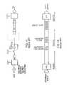
- FIG. 1( a )An example of a three stage column address pipeline is shown in the schematic diagram of FIG. 1( a ).
- the column address-to-output partis a three stage pipeline.
- the address bufferis the first latch.
- the column switchis the second latch and the output buffer is the third latch. The latency inherent in the column access time is therefore divided up between these three stages.
- the operation of pipelined readmay be explained as follows: the column address ( 1 ) is clocked into the address buffer on one clock cycle and is decoded. On the second clock cycle, the column switch transfers the corresponding data (D 1 ) from the sense amplifier to the read bus and column address (A 2 ) is clocked into the address buffer. On clock three, the data (D 1 ) is clocked into the output buffer, (D 2 ) is transferred to the read bus and A 3 is clocked into the column address buffer. When D 1 appears at the output, D 2 and D 3 are in the pipeline behind it.
- the readeris referred to a book entitled “High Performance Memories” by Betty Prince.
- the delay in the number of clock cycles between the latching CAS in a SDRAM and the availability of the data busis the “CAS latency” of the SDRAM. If the output data is available by the second leading edge of the clock following arrival of a column address, the device is described as having a CAS latency of two. Similarly, if the data is available at the third leading edge of the clock following the arrival of the first read command, the device is known as having a “CAS latency” of three.
- Synchronous DRAMscome with programmable CAS latencies. As described above, the CAS latency determines at which clock edge cycle data will be available after a read command is initiated, regardless of the clock rate (CLK). The programmable CAS latencies enable SDRAMs to be efficiently utilized in different memory systems having different system clock frequencies without affecting the CAS latency.
- a wave pipelineis shown schematically in FIG. 1( b ).
- a regular clocked pipelinehas the disadvantage that the read latency will be equal to the delay of the slowest pipeline stage (i.e. longest delay) multiplied by the number of pipeline stages.
- a clocked pipeline with adjusted clocksuses clock signals that have been adjusted to each pipeline stage so that longer pipeline stages may be accommodated without impacting the read latency.
- a longer pipeline stagewill be ended with a clock that is more delayed than the clock that starts the pipeline stage.
- a shorter pipeline stagewill be started with a clock that is more delayed than the clock that ends the pipeline stage.
- a disadvantage of this schemeis that different adjustments to the clock are needed for each CAS latency supported by the chip.
- architecture changescan have a large impact on the breakdown of the latency stages, requiring designers to readjust all the clocks to accommodate the new division of latency stages.
- Latency stagecan be inserted without adding extra latency or chip area.
- Multiple latency stageshave a disadvantage in that not all latency stages will be equal in the time needed for signals to propagate through the stage.
- Another complicationis the need to enable or disable latency stages depending on the CAS latency at which the chip has been programmed to operate.
- a wave pipelineIn the wave pipeline of FIG. 1( b ) runs pulses of data through the entire read data path.
- a wave pipelinerelies on an ideal data path length, that is it assumes that all data paths are equal.
- data retrieved from certain memory cells in a memory arraywill be inherently faster than data retrieval from other memory cells. This is primarily due to the physical location of the memory cells relative to both the read in and read out data path. Thus data must be resynchronized before being output from the chip. This data path skew makes it difficult to safely resynchronize the retrieved data in a wave pipeline implementation.
- address signalsare applied to a data path with a cycle time which exceeds the memory access time, then the data which is read from the memory is not output during the inherent delay of the memory core.
- address input signalsare applied with a period, which is less than the critical path of the memory core section.
- the present inventionthus seeks to mitigate at least some of the various disadvantages described with respect to the current art.
- pipelined SDRAMcomprising:
- asynchronous control signalsare generated within the chip and optimized to the different latency stages.
- a still further aspect of the inventionprovides stages that are independent of the system clock thereby allowing the read data path to be run at any CAS latency which may be supported by a suitable resynchronizing output.
- a still further aspect of the inventionprovides for a synchronization circuit coupled to the end of the read data path for synchronizing the output data to a system clock.
- FIG. 1( a )is a schematic diagram of a conventional clocked pipeline memory circuit
- FIG. 1( b )is a schematic diagram of a conventional wave pipeline memory circuit
- FIGS. 2( a ) and 2 ( b )are timing waveforms for a SDRAM having a CAS latency of 3 running under fast and slow clock conditions respectively;
- FIG. 3is a schematic diagram of a generalized embodiment of the present invention.
- FIG. 4is a more detailed schematic diagram of the generalized embodiment of FIG. 3 ;
- FIG. 5is a timing waveform diagram according to a first embodiment of the present invention.
- FIGS. 6( a ), 6 ( b ) and 6 ( c )show detailed circuit diagrams of a pipe control circuit according to an embodiment of the present invention
- FIGS. 7( a ), 7 ( b ) and 7 ( c )show detailed circuit diagrams for a pipe latch and data output latch according to an embodiment of the present invention.
- FIG. 8is a schematic diagram of a data output control circuit according to an embodiment of the present invention.
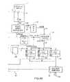
- FIG. 3a schematic diagram of a pipelined semiconductor memory according to a generalized embodiment of the invention is shown generally by numeral 20 .
- the memoryincludes a core memory array 22 having a read path 24 , defined between an address input port 25 and a data output 32 .
- the read path 24is broken up into latency stages 27 , each of which is latched by respective asynchronous control signals 28 .
- a synchronizing circuit 30is coupled to the last latency stage of the read path in order to resynchronize the data to the system clock CLK at output 32 of the read path.
- the datais synchronized to the system clock CLK a predetermined number of clock cycles after the application of an address signal A to the address input 25 , i.e. depending on the CAS latency of the system.
- the segmentation of the read path 23 into the three main latency stages, each controlled by respective control signals 28illustrates, in general, the combining of clocked and wave pipeline techniques to achieve an asynchronous pipeline implementation according to the invention which exhibits less skew than a conventional wave pipeline but which allows for operation with any CAS latency without having to adjust individual clocks in each stage as would be required in a clocked pipeline implementation.
- FIG. 3serves to provide an overview of the detailed circuits discussed below.
- the latency stages 26 in FIG. 3include an address input latch 42 , for receiving an address signal Ai at the address input port 25 , the output of which is coupled to an address pre-decoder latch 44 which is in turn connected to a column address decoder latch 46 .
- the column address decoder latch 46decodes the address signal and is coupled to select memory cells 48 in the memory cell array 22 .
- the column address decoder 46activates relevant sense amplifiers (not shown) for detecting the data read out from a selected memory cell 48 .
- the output of the sense amplifiersis coupled to a read main amplifier block 50 via a local databus DB, which is 32-bits wide in this embodiment,
- the output of the read main amplifier 50is coupled to a global databus GDB.
- a multiplexer 52multiplexes the GDB onto an I/O databus IODB, which is in turn coupled to a read databus amplifier RDBAMP latch block 54 .
- the synchronizing circuit 30 of FIG. 3is comprised of pipe latches 56 , an output buffer 58 and control circuitry shown by block 61 . More specifically, the output from the RDBAMP latch is selectively coupled to the input of three pipe latches pipe_latchO, pipe_latch 1 and pipe_latch 2 as will be described below. The outputs from the pipe latches are connected together and coupled to the input of the output buffer 58 .
- the memoryalso includes a command latch circuit 62 having a clock input terminal coupled to the system clock CLK and a command input terminal for receiving command signals such as RAS , CAS , CS .
- the command latch 62provides a first control signal 64 , which is rn through a series of control logic and delay elements T 1 to T 4 .
- Each of the delay elements T 1 , T 2 , T 3 and T 4produce respective delayed control signals that are fed to an input latch terminal of the pre-decoder latch 44 , the Y decoder 46 , the RMA 50 and the RDBAMP latch 54 , respectively. These signals serve as individual asynchronous control signals for these circuits.
- the address latch clock inputis derived directly from the system clock signal CLK.
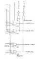
- Pipe latch control circuitry 61Control of the pipe latches pipe_latch 0 , pipe_latch 1 and pipe_latch 2 is provided by the pipe latch control circuitry 61 .
- Each pipe latchis driven by a respective pipe latch enable signal, latch_enx( 0 ), latch_enx( 1 ) and latch_enx( 2 ) coupled to its latch input enable terminal.
- the pipe latch enable signalsare derived from a pipe counter 64 which produces three count signals COUNT.
- the pipe counteris a free running counter which resets its count based on the total number of pipe latches. After a preset number of clock counts set by the system clock signal coupled to the pipe counter clock input terminal.
- the output COUNT signals from the pipe counterare coupled via count delay elements 66 to count synchronization latches 68 .
- the outputs from the three latches 68provide the pipe latch enable signal for clocking the appropriate pipe latch 56 .
- the clock input enable terminal of the lathes 68are coupled to the asynchronous control signal of the latency stage in the read path, in this case, signal IODB_READX of the RDBAMP 54 to ensure the pipe latch is latched at the appropriate time.
- the count delay circuitry 66could be segmented into multiple delay stages, each receiving control logic enable signals such as YSG or Y_EXTRD. The timing relationship between the address propagation and data retrieval and the clock count delay would therefore be more closely matched.
- the output COUNT of pipe counter 64is connected to a pipe delay element 70 for generating a pipe latch output enable signal QEN_RISEX which is connected to the respective output enable terminal of the pipe latches 56 .
- a CLK_IO signalwhich is DLL generated and slightly leads the system clock CLK, is coupled to an output enable terminal of the pipe delay and the output buffer 58 .
- the DLLdelay locked loop
- the address latch 42latches the external address signal Ai, which is then free to propagate to pre-decoder latch 44 which latches the address after a delay T 1 set by the delay element T 1 .
- These address signalsare decoded in the Y decoder 46 and latched by the signal YSG delayed from CLK by T 1 and T 2 .
- the appropriate columnsare activated and data is read out from the memory cells into column sense amplifiers and then latched in the RMA 50 by the IOREAD signal which is delayed from CLK by T 1 +T 2 +T 3 .
- the datais available on the global data bus GDB.
- the RDBAMP 54may now be latched at time t 1 by signal IODB_READ that is delayed from IOREAD by T 4 , to provide the DOUTE signal.
- these asynchronous control signalsare used to control the pipeline stages. These signals control when data is read into the latch (usually a latched amplifier). Once read into the latch, data is free to propagate toward the next stage Each control signal is generated by delaying the control signal from the previous latency stage. The first stage is started by the external clock CLK. The next stage will latch data from the previous stage on the control signal that is delayed from the external clock. It may be noted that some of these delays are inherent in the circuits used to control whether a read is to take place, while some of the delays are deliberately added using timing delay elements. These are usually comprised of buffers sized to run slowly and which may include additional resistive or capacitive elements.
- the delays T 1 to T 4can be optimized to the particular memory independent of the external clock timing.
- the delay for each of these latchesis selected to accommodate the propagation delays between these blocks.
- the clock signal applied to the read main amplifier latchis synchronized and delayed from the clock signal applied to the column decoder latch to accommodate the lag in retrieving data from different areas of the memory array 22 to the read main amplifier 50 .
- the data once latched in the RDBAMP 54 at time t 1must as with the conventional wave pipelines, be resynchronized to the system clock CLK at the output 32 of the memory. This is accomplished as follows.
- the pipe latches 56allow data to be stored in the event of fast data or a slow clock. Generally, the number of latches needed is equivalent to the number of latency stages to be supported.
- a COUNT signalis delayed asynchronously by the count delay element 66 and clocked by the control signal for the last stage in this case IODB_READ into a clock synchronizing latch 68 .
- This time delayed COUNT signalgenerates LATCH_EN which determines which of the latches 56 the data from RDBAMP 54 is to be stored in. Furthermore the COUNT signal is also delayed by the appropriate number of clock cycles, as determined by the current CAS latency to which the chip is programmed. This clock delayed COUNT signal shown as QEN_RISE in FIG. 5 controls which of the latches 56 has its output enabled to output data to the output buffer 58 .
- a CNT_DEL signalis generated which is combined in the clock synchronizing latch 68 with the IODB_READX signal to generate the LATCH_ENX signal.
- the latches 56work as a FIFO register, with the first data input to one of the set of latches 56 , being the first data to be output from the set of latches.
- the latches in the read pathsegment the path into latency stages of an asynchronous pipeline.
- the chip architecture and the maximum operating frequencydetermine the number and placement of these stages. In general, a higher operating frequency will require a large number of shorter pipeline stages.
- Other techniquescan be used such as doubling the number of data paths in a stage and alternating between the data paths. For example, a read output from the sense amplifiers is alternated between two data buses. This is described in Mosaid U.S. Pat. No. 5,416,743.
- the placement of the stageswill generally be dictated by the position of amplifiers or buffers, which may be converted into latches without resulting in extensive area penalty.
- latency stagesrefer to any circuit element capable of introducing a delay in the signal or data path.
- the pipe control circuitry 61includes a pipe counter 90 , a detailed schematic of which is shown in FIG. 6 b , for producing a two digit binary count, COUNT 0 and COUNT 1, determined by the input system clock frequency at its clock input terminal CLK.
- Each of the count lines, COUNT 1 and COUNT 0are connected to respective count delay elements 92 and 94 .
- the delayed count signalsare connected to a count decoder 96 which decodes the input binary count to activate one of the three count delay lines 98 , CNTO_DEL, CNT 1 _DEL, CNT 2 _DEL.
- the signals on these delayed count lines 98correspond to the COUNT signal as shown in FIG. 5 .
- the delayed COUNT signals 98are coupled to the inputs of respective clocked latches 100 , the outputs of which are buffered and provide the respective latch enable signal referred to in FIG. 5 , LATCH_ENX( 0 ), LATCH_ENX( 1 ), LATCH_EN( 2 ).
- the clock input terminal of these latches 100is coupled to the IODB_READ asynchronous control signal from the last latency stage via an inverter.
- the pipe counter 90also has its output connected to a second decoder 102 also providing respective count signals, CNT 0, CNT 1 and CNT 2, which are coupled to respective pipe delay elements 104 , 106 and 108 .
- a detailed circuit diagram of the pipe delay circuit implementationis shown in FIG. 6 c .
- the output of the pipe delayis controlled by a CLK_IO signal and generates the QEN_RISE signal referred to in FIG. 5 connected to the output latch enable of the pipe latches 56 .
- Corresponding QEN_FALL signalsare generated for the falling edge of the system clock whereas QEN_RISE corresponds to the rising edge of the system clock.
- FIGS. 7 a and 7 ba detailed schematic of the pipe latches 56 and the output buffer circuitry is shown
- the data bits from the IODB databusare received at the input of the RDB amplifiers 110 .
- Two RDBAMPSare shown in this implementation because of the double data rate (DDR) where data is clocked on both the rise and fall edges of the system clock.
- the outputs from the RDBAMPSare connected to a series of six pipe latches 112 to 122 .
- Six latchesare required instead of three due to the DDR implementation.
- the enable inputs of the pipe latches 112 to 122are coupled to the respective latch enable signals derived from the circuit of FIG. 6 a .
- the top three pipe latches 112 to 116have their outputs connected to inputs of a 3 OR 2 NAND gate 124 .
- the bottom three latches 118 to 122have the outputs connected to a 3 OR 2 NAND gates 126 .
- the QEN_RISE signalis connected to the inputs of the 3 OR 2 NAND gate 124 , the output of which, when enabled, couples data to the DOUT_RISE, DOUT_RISEX input of the output buffer shown in FIG. 7 b .
- a system clock control signal EDGEis provided for directing data to the top three or bottom three latches, once again a DDR feature.
- the data output buffer 58 as shown in FIG. 4is comprised of data output latches 130 to 136 .
- the input enable terminals of the data output latches 130 to 136are coupled to the CLK_ 10 signal for synchronizing to the correct system clock edge.
- a detailed circuit implementation of the pipe latches 112 to 122is shown in FIG. 7 c.
- the present inventionprovides a flexible method for implementing a pipelined semiconductor memory, which can easily accommodate both a fast and slow system clock. Furthermore, the flexible design allows further segmentation of the read path for more precise matching of internal signals. Furthermore, various CAS latencies may be accommodated by simply delaying the output from the pipe delay element 70 to wait a specific number of clock cycles before clocking the data out.
Landscapes
- Engineering & Computer Science (AREA)
- Microelectronics & Electronic Packaging (AREA)
- Computer Hardware Design (AREA)
- Dram (AREA)
- Static Random-Access Memory (AREA)
Abstract
Description
Claims (16)
Priority Applications (6)
| Application Number | Priority Date | Filing Date | Title |
|---|---|---|---|
| US11/673,834US7509469B2 (en) | 1998-04-01 | 2007-02-12 | Semiconductor memory asynchronous pipeline |
| US12/371,255US7865685B2 (en) | 1998-04-01 | 2009-02-13 | Semiconductor memory asynchronous pipeline |
| US12/773,531US8078821B2 (en) | 1998-04-01 | 2010-05-04 | Semiconductor memory asynchronous pipeline |
| US13/049,487US8122218B2 (en) | 1998-04-01 | 2011-03-16 | Semiconductor memory asynchronous pipeline |
| US13/327,154US8601231B2 (en) | 1998-04-01 | 2011-12-15 | Semiconductor memory asynchronous pipeline |
| US14/089,242US9548088B2 (en) | 1998-04-01 | 2013-11-25 | Semiconductor memory asynchronous pipeline |
Applications Claiming Priority (6)
| Application Number | Priority Date | Filing Date | Title |
|---|---|---|---|
| CA2233789 | 1998-04-01 | ||
| CA2233789ACA2233789C (en) | 1998-04-01 | 1998-04-01 | Semiconductor memory asynchronous pipeline |
| US09/129,878US6539454B2 (en) | 1998-04-01 | 1998-08-06 | Semiconductor memory asynchronous pipeline |
| US10/290,317US6772312B2 (en) | 1998-04-01 | 2002-11-08 | Semiconductor memory having asynchronous pipeline stages |
| US10/855,968US7178001B2 (en) | 1998-04-01 | 2004-05-28 | Semiconductor memory asynchronous pipeline |
| US11/673,834US7509469B2 (en) | 1998-04-01 | 2007-02-12 | Semiconductor memory asynchronous pipeline |
Related Parent Applications (1)
| Application Number | Title | Priority Date | Filing Date |
|---|---|---|---|
| US10/855,968ContinuationUS7178001B2 (en) | 1998-04-01 | 2004-05-28 | Semiconductor memory asynchronous pipeline |
Related Child Applications (1)
| Application Number | Title | Priority Date | Filing Date |
|---|---|---|---|
| US12/371,255ContinuationUS7865685B2 (en) | 1998-04-01 | 2009-02-13 | Semiconductor memory asynchronous pipeline |
Publications (2)
| Publication Number | Publication Date |
|---|---|
| US20070186034A1 US20070186034A1 (en) | 2007-08-09 |
| US7509469B2true US7509469B2 (en) | 2009-03-24 |
Family
ID=25680118
Family Applications (8)
| Application Number | Title | Priority Date | Filing Date |
|---|---|---|---|
| US10/290,317Expired - LifetimeUS6772312B2 (en) | 1998-04-01 | 2002-11-08 | Semiconductor memory having asynchronous pipeline stages |
| US10/855,968Expired - LifetimeUS7178001B2 (en) | 1998-04-01 | 2004-05-28 | Semiconductor memory asynchronous pipeline |
| US11/673,834Expired - Fee RelatedUS7509469B2 (en) | 1998-04-01 | 2007-02-12 | Semiconductor memory asynchronous pipeline |
| US12/371,255Expired - Fee RelatedUS7865685B2 (en) | 1998-04-01 | 2009-02-13 | Semiconductor memory asynchronous pipeline |
| US12/773,531Expired - Fee RelatedUS8078821B2 (en) | 1998-04-01 | 2010-05-04 | Semiconductor memory asynchronous pipeline |
| US13/049,487Expired - Fee RelatedUS8122218B2 (en) | 1998-04-01 | 2011-03-16 | Semiconductor memory asynchronous pipeline |
| US13/327,154Expired - Fee RelatedUS8601231B2 (en) | 1998-04-01 | 2011-12-15 | Semiconductor memory asynchronous pipeline |
| US14/089,242Expired - Fee RelatedUS9548088B2 (en) | 1998-04-01 | 2013-11-25 | Semiconductor memory asynchronous pipeline |
Family Applications Before (2)
| Application Number | Title | Priority Date | Filing Date |
|---|---|---|---|
| US10/290,317Expired - LifetimeUS6772312B2 (en) | 1998-04-01 | 2002-11-08 | Semiconductor memory having asynchronous pipeline stages |
| US10/855,968Expired - LifetimeUS7178001B2 (en) | 1998-04-01 | 2004-05-28 | Semiconductor memory asynchronous pipeline |
Family Applications After (5)
| Application Number | Title | Priority Date | Filing Date |
|---|---|---|---|
| US12/371,255Expired - Fee RelatedUS7865685B2 (en) | 1998-04-01 | 2009-02-13 | Semiconductor memory asynchronous pipeline |
| US12/773,531Expired - Fee RelatedUS8078821B2 (en) | 1998-04-01 | 2010-05-04 | Semiconductor memory asynchronous pipeline |
| US13/049,487Expired - Fee RelatedUS8122218B2 (en) | 1998-04-01 | 2011-03-16 | Semiconductor memory asynchronous pipeline |
| US13/327,154Expired - Fee RelatedUS8601231B2 (en) | 1998-04-01 | 2011-12-15 | Semiconductor memory asynchronous pipeline |
| US14/089,242Expired - Fee RelatedUS9548088B2 (en) | 1998-04-01 | 2013-11-25 | Semiconductor memory asynchronous pipeline |
Country Status (7)
| Country | Link |
|---|---|
| US (8) | US6772312B2 (en) |
| EP (1) | EP1068619B1 (en) |
| JP (1) | JP2002510118A (en) |
| CN (1) | CN1154111C (en) |
| AU (1) | AU3021799A (en) |
| DE (1) | DE69923769T2 (en) |
| WO (1) | WO1999050852A1 (en) |
Cited By (2)
| Publication number | Priority date | Publication date | Assignee | Title |
|---|---|---|---|---|
| US20090175103A1 (en)* | 1998-04-01 | 2009-07-09 | Mosaid Technologies Incorporated | Semiconductor memory asynchronous pipeline |
| US20090238014A1 (en)* | 2008-03-19 | 2009-09-24 | Chia-Jen Chang | Low power synchronous memory command address scheme |
Families Citing this family (52)
| Publication number | Priority date | Publication date | Assignee | Title |
|---|---|---|---|---|
| US6516363B1 (en) | 1999-08-06 | 2003-02-04 | Micron Technology, Inc. | Output data path having selectable data rates |
| US6694416B1 (en) | 1999-09-02 | 2004-02-17 | Micron Technology, Inc. | Double data rate scheme for data output |
| JP3482996B2 (en)* | 1999-12-03 | 2004-01-06 | 日本電気株式会社 | ATM switch |
| EP1122737A1 (en)* | 2000-01-31 | 2001-08-08 | STMicroelectronics S.r.l. | Circuit for managing the transfer of data streams from a plurality of sources within a system |
| US6788593B2 (en) | 2001-02-28 | 2004-09-07 | Rambus, Inc. | Asynchronous, high-bandwidth memory component using calibrated timing elements |
| US6675272B2 (en) | 2001-04-24 | 2004-01-06 | Rambus Inc. | Method and apparatus for coordinating memory operations among diversely-located memory components |
| EP1253521B1 (en)* | 2001-04-24 | 2011-01-26 | Rambus Inc. | Method and apparatus for signaling between devices of a memory system |
| US8391039B2 (en) | 2001-04-24 | 2013-03-05 | Rambus Inc. | Memory module with termination component |
| DE10121165B4 (en)* | 2001-04-30 | 2011-02-03 | Qimonda Ag | Method and apparatus for initializing an asynchronous latch chain |
| US7028167B2 (en)* | 2002-03-04 | 2006-04-11 | Hewlett-Packard Development Company, L.P. | Core parallel execution with different optimization characteristics to decrease dynamic execution path |
| KR100520677B1 (en)* | 2003-04-28 | 2005-10-11 | 주식회사 하이닉스반도체 | Data input device in a synchronous semiconductor memory device and method of inputting a data using the same |
| US6970395B2 (en)* | 2003-09-08 | 2005-11-29 | Infineon Technologies Ag | Memory device and method of reading data from a memory device |
| US6856270B1 (en) | 2004-01-29 | 2005-02-15 | International Business Machines Corporation | Pipeline array |
| US7301831B2 (en) | 2004-09-15 | 2007-11-27 | Rambus Inc. | Memory systems with variable delays for write data signals |
| US7549092B2 (en)* | 2005-09-29 | 2009-06-16 | Hynix Semiconductor, Inc. | Output controller with test unit |
| WO2007065308A1 (en)* | 2005-12-10 | 2007-06-14 | Intel Corporation | Speculative code motion for memory latency hiding |
| CN100458973C (en)* | 2006-05-17 | 2009-02-04 | 中国人民解放军国防科学技术大学 | High speed streamline long-time-delay multi-port SRAM quick access method |
| US7564738B2 (en)* | 2006-08-11 | 2009-07-21 | Freescale Semiconductor, Inc. | Double-rate memory |
| KR100895072B1 (en)* | 2007-03-08 | 2009-04-27 | 삼성전자주식회사 | Memory system that can guarantee the stability of read data and its data reading method |
| US7865756B2 (en)* | 2007-03-12 | 2011-01-04 | Mosaid Technologies Incorporated | Methods and apparatus for clock signal synchronization in a configuration of series-connected semiconductor devices |
| CN101295537B (en)* | 2007-04-24 | 2010-10-27 | 南亚科技股份有限公司 | Method for controlling read operation of memory |
| US8781053B2 (en) | 2007-12-14 | 2014-07-15 | Conversant Intellectual Property Management Incorporated | Clock reproducing and timing method in a system having a plurality of devices |
| US8467486B2 (en)* | 2007-12-14 | 2013-06-18 | Mosaid Technologies Incorporated | Memory controller with flexible data alignment to clock |
| US7800974B2 (en)* | 2008-02-21 | 2010-09-21 | Freescale Semiconductor, Inc. | Adjustable pipeline in a memory circuit |
| US8266471B2 (en)* | 2010-02-09 | 2012-09-11 | Mosys, Inc. | Memory device including a memory block having a fixed latency data output |
| US8635487B2 (en)* | 2010-03-15 | 2014-01-21 | International Business Machines Corporation | Memory interface having extended strobe burst for write timing calibration |
| US8856579B2 (en)* | 2010-03-15 | 2014-10-07 | International Business Machines Corporation | Memory interface having extended strobe burst for read timing calibration |
| US8711639B2 (en) | 2010-11-02 | 2014-04-29 | Micron Technology, Inc. | Data paths using a first signal to capture data and a second signal to output data and methods for providing data |
| US8826057B1 (en) | 2012-03-30 | 2014-09-02 | Integrated Device Technology Inc. | Multiple time domain synchronizer circuits |
| US8943242B1 (en)* | 2012-03-30 | 2015-01-27 | Integrated Device Technology Inc. | Timing controllers having partitioned pipelined delay chains therein |
| US9431110B2 (en)* | 2012-09-26 | 2016-08-30 | Intel Corporation | Column address decoding |
| US9159391B1 (en)* | 2012-12-13 | 2015-10-13 | Gsi Technology, Inc. | Systems and methods of double/quad data rate memory involving input latching, self-timing and/or other features |
| US9431079B1 (en) | 2012-12-13 | 2016-08-30 | Gsi Technology, Inc. | Systems and methods of memory and memory operation involving input latching, self-timing and/or other features |
| EP3014468A4 (en) | 2013-09-06 | 2017-06-21 | Huawei Technologies Co., Ltd. | Method and apparatus for asynchronous processor with auxiliary asynchronous vector processor |
| KR102101390B1 (en)* | 2013-10-08 | 2020-04-17 | 에스케이하이닉스 주식회사 | Semiconductor device and semiconductor system including thereof |
| KR102200489B1 (en)* | 2014-05-30 | 2021-01-11 | 삼성전자주식회사 | Nonvolatile memory device and storage device having the same |
| KR20160029382A (en)* | 2014-09-05 | 2016-03-15 | 에스케이하이닉스 주식회사 | Semiconductor Memory Apparatus |
| WO2016081192A1 (en) | 2014-11-20 | 2016-05-26 | Rambus Inc. | Memory systems and methods for improved power management |
| US9734127B2 (en)* | 2015-02-05 | 2017-08-15 | Weng Tianxiang | Systematic method of synthesizing wave-pipelined circuits in HDL |
| US10019170B2 (en) | 2016-03-30 | 2018-07-10 | Micron Technology, Inc. | Controlling timing and edge transition of a delayed clock signal and data latching methods using such a delayed clock signal |
| KR102743477B1 (en) | 2016-12-21 | 2024-12-16 | 에스케이하이닉스 주식회사 | Semiconductor device |
| US10170166B1 (en) | 2017-09-08 | 2019-01-01 | Winbond Electronics Corp. | Data transmission apparatus for memory and data transmission method thereof |
| KR102585218B1 (en) | 2017-09-28 | 2023-10-05 | 삼성전자주식회사 | Non-volatile memory device and storage device including the same |
| US10410698B2 (en) | 2017-12-07 | 2019-09-10 | Micron Technology, Inc. | Skew reduction of a wave pipeline in a memory device |
| US10360956B2 (en) | 2017-12-07 | 2019-07-23 | Micron Technology, Inc. | Wave pipeline |
| KR102517462B1 (en)* | 2018-04-23 | 2023-04-05 | 에스케이하이닉스 주식회사 | Semiconductor device |
| KR102708728B1 (en) | 2019-01-15 | 2024-09-23 | 에스케이하이닉스 주식회사 | Semiconductor device and semiconductor system |
| US11061836B2 (en)* | 2019-06-21 | 2021-07-13 | Micron Technology, Inc. | Wave pipeline including synchronous stage |
| US11055220B2 (en) | 2019-08-19 | 2021-07-06 | Truememorytechnology, LLC | Hybrid memory systems with cache management |
| US11526441B2 (en) | 2019-08-19 | 2022-12-13 | Truememory Technology, LLC | Hybrid memory systems with cache management |
| US12189460B2 (en)* | 2021-07-06 | 2025-01-07 | UPBEAT TECHNOLOGY Co., Ltd | Error detection and correction method and circuit |
| KR20240132941A (en) | 2023-02-27 | 2024-09-04 | 에스케이하이닉스 주식회사 | Data input output device for performing data input output operation using pipe circuit |
Citations (17)
| Publication number | Priority date | Publication date | Assignee | Title |
|---|---|---|---|---|
| US4658354A (en) | 1982-05-28 | 1987-04-14 | Nec Corporation | Pipeline processing apparatus having a test function |
| US5272390A (en) | 1991-09-23 | 1993-12-21 | Digital Equipment Corporation | Method and apparatus for clock skew reduction through absolute delay regulation |
| US5294842A (en) | 1991-09-23 | 1994-03-15 | Digital Equipment Corp. | Update synchronizer |
| US5402388A (en) | 1993-12-16 | 1995-03-28 | Mosaid Technologies Incorporated | Variable latency scheme for synchronous memory |
| EP0704848A2 (en) | 1994-09-28 | 1996-04-03 | Nec Corporation | Semiconductor pipeline memory device eliminating time loss due to difference between pipeline stages from data access |
| US5544124A (en) | 1995-03-13 | 1996-08-06 | Micron Technology, Inc. | Optimization circuitry and control for a synchronous memory device with programmable latency period |
| US5550784A (en) | 1994-09-28 | 1996-08-27 | Nec Corporation | Semiconductor memory device with synchronous dram whose speed grade is not limited |
| JPH0991955A (en) | 1995-09-20 | 1997-04-04 | Nec Corp | Semiconductor memory |
| US5655105A (en) | 1995-06-30 | 1997-08-05 | Micron Technology, Inc. | Method and apparatus for multiple latency synchronous pipelined dynamic random access memory |
| US5666480A (en) | 1991-11-05 | 1997-09-09 | Monolithic System Technology, Inc. | Fault-tolerant hierarchical bus system and method of operating same |
| US5703815A (en) | 1995-03-24 | 1997-12-30 | Nec Corporation | High-speed semiconductor memory system |
| US5713005A (en) | 1995-02-10 | 1998-01-27 | Townsend And Townsend And Crew Llp | Method and apparatus for pipelining data in an integrated circuit |
| US5784705A (en) | 1996-07-15 | 1998-07-21 | Mosys, Incorporated | Method and structure for performing pipeline burst accesses in a semiconductor memory |
| USRE35934E (en) | 1993-04-02 | 1998-10-27 | Nec Corporation | Semiconductor memory device synchronous with external clock signal for outputting data bits through a small number of data lines |
| US6014339A (en) | 1997-04-03 | 2000-01-11 | Fujitsu Limited | Synchronous DRAM whose power consumption is minimized |
| US6078546A (en) | 1997-03-18 | 2000-06-20 | Samsung Electronics Co., Ltd. | Synchronous semiconductor memory device with double data rate scheme |
| US6539454B2 (en) | 1998-04-01 | 2003-03-25 | Mosaid Technologies Incorporated | Semiconductor memory asynchronous pipeline |
Family Cites Families (32)
| Publication number | Priority date | Publication date | Assignee | Title |
|---|---|---|---|---|
| KR960003526B1 (en) | 1992-10-02 | 1996-03-14 | 삼성전자주식회사 | Semiconductor memory device |
| JPH023177A (en)* | 1988-03-11 | 1990-01-08 | Hitachi Ltd | Semiconductor integrated circuit |
| US6757809B1 (en)* | 1989-12-16 | 2004-06-29 | Renesas Technology Corp. | Data processor having 2n bits width data bus for context switching functions |
| JP2796590B2 (en)* | 1991-08-07 | 1998-09-10 | 三菱電機株式会社 | Memory device and data processing device using the same |
| JPH05144269A (en) | 1991-11-19 | 1993-06-11 | Fujitsu Ltd | Semiconductor memory device |
| US5452324A (en)* | 1992-09-23 | 1995-09-19 | Texas Instruments Incorporated | Packet data recovery system |
| JPH06187787A (en) | 1992-12-17 | 1994-07-08 | Hitachi Ltd | Semiconductor memory and control method for operation of its pipe line |
| JP3078934B2 (en) | 1992-12-28 | 2000-08-21 | 富士通株式会社 | Synchronous random access memory |
| US5384737A (en)* | 1994-03-08 | 1995-01-24 | Motorola Inc. | Pipelined memory having synchronous and asynchronous operating modes |
| JP3177094B2 (en) | 1994-05-31 | 2001-06-18 | 富士通株式会社 | Semiconductor storage device |
| JPH0831180A (en) | 1994-07-08 | 1996-02-02 | Hitachi Ltd | Semiconductor memory device |
| TW367656B (en) | 1994-07-08 | 1999-08-21 | Hitachi Ltd | Semiconductor memory device |
| US5796673A (en)* | 1994-10-06 | 1998-08-18 | Mosaid Technologies Incorporated | Delay locked loop implementation in a synchronous dynamic random access memory |
| JP3543181B2 (en)* | 1994-11-09 | 2004-07-14 | 株式会社ルネサステクノロジ | Data processing device |
| JP3497615B2 (en)* | 1995-07-12 | 2004-02-16 | 矢崎総業株式会社 | Female terminal |
| JPH0963262A (en) | 1995-08-17 | 1997-03-07 | Fujitsu Ltd | Synchronous DRAM |
| JP2907074B2 (en) | 1995-08-25 | 1999-06-21 | 日本電気株式会社 | Semiconductor storage device |
| KR0164395B1 (en) | 1995-09-11 | 1999-02-18 | 김광호 | Semiconductor memory device and grid and write method |
| JP3183321B2 (en)* | 1995-11-10 | 2001-07-09 | 日本電気株式会社 | Semiconductor storage device |
| JP3183159B2 (en)* | 1996-03-29 | 2001-07-03 | 日本電気株式会社 | Synchronous DRAM |
| US6209071B1 (en) | 1996-05-07 | 2001-03-27 | Rambus Inc. | Asynchronous request/synchronous data dynamic random access memory |
| JP4070255B2 (en)* | 1996-08-13 | 2008-04-02 | 富士通株式会社 | Semiconductor integrated circuit |
| JPH10188556A (en)* | 1996-12-20 | 1998-07-21 | Fujitsu Ltd | Semiconductor storage device |
| JP3856892B2 (en)* | 1997-03-03 | 2006-12-13 | 日本電信電話株式会社 | Self-synchronous pipeline data path circuit and asynchronous signal control circuit |
| US5999258A (en)* | 1997-06-26 | 1999-12-07 | Nortel Networks Corporation | Optical interference measurement method and system |
| JP3901297B2 (en)* | 1997-09-09 | 2007-04-04 | 富士通株式会社 | DLL circuit and semiconductor memory device using the same |
| US6289494B1 (en)* | 1997-11-12 | 2001-09-11 | Quickturn Design Systems, Inc. | Optimized emulation and prototyping architecture |
| JPH11176158A (en) | 1997-12-10 | 1999-07-02 | Fujitsu Ltd | Latch circuit, data output circuit, and semiconductor device having the same |
| US6067648A (en)* | 1998-03-02 | 2000-05-23 | Tanisys Technology, Inc. | Programmable pulse generator |
| JP2002510118A (en)* | 1998-04-01 | 2002-04-02 | モサイド・テクノロジーズ・インコーポレーテッド | Semiconductor memory asynchronous pipeline |
| WO2002005281A2 (en) | 2000-07-07 | 2002-01-17 | Mosaid Technologies Incorporated | A high speed dram architecture with uniform access latency |
| KR100391151B1 (en) | 2000-11-20 | 2003-07-12 | 삼성전자주식회사 | synchronous semiconductor memory and method for operating same |
- 1999
- 1999-04-01JPJP2000541688Apatent/JP2002510118A/ennot_activeWithdrawn
- 1999-04-01WOPCT/CA1999/000282patent/WO1999050852A1/enactiveIP Right Grant
- 1999-04-01AUAU30217/99Apatent/AU3021799A/ennot_activeAbandoned
- 1999-04-01EPEP99911552Apatent/EP1068619B1/ennot_activeExpired - Lifetime
- 1999-04-01DEDE69923769Tpatent/DE69923769T2/ennot_activeExpired - Lifetime
- 1999-04-01CNCNB998049085Apatent/CN1154111C/ennot_activeExpired - Lifetime
- 2002
- 2002-11-08USUS10/290,317patent/US6772312B2/ennot_activeExpired - Lifetime
- 2004
- 2004-05-28USUS10/855,968patent/US7178001B2/ennot_activeExpired - Lifetime
- 2007
- 2007-02-12USUS11/673,834patent/US7509469B2/ennot_activeExpired - Fee Related
- 2009
- 2009-02-13USUS12/371,255patent/US7865685B2/ennot_activeExpired - Fee Related
- 2010
- 2010-05-04USUS12/773,531patent/US8078821B2/ennot_activeExpired - Fee Related
- 2011
- 2011-03-16USUS13/049,487patent/US8122218B2/ennot_activeExpired - Fee Related
- 2011-12-15USUS13/327,154patent/US8601231B2/ennot_activeExpired - Fee Related
- 2013
- 2013-11-25USUS14/089,242patent/US9548088B2/ennot_activeExpired - Fee Related
Patent Citations (19)
| Publication number | Priority date | Publication date | Assignee | Title |
|---|---|---|---|---|
| US4658354A (en) | 1982-05-28 | 1987-04-14 | Nec Corporation | Pipeline processing apparatus having a test function |
| US5272390A (en) | 1991-09-23 | 1993-12-21 | Digital Equipment Corporation | Method and apparatus for clock skew reduction through absolute delay regulation |
| US5294842A (en) | 1991-09-23 | 1994-03-15 | Digital Equipment Corp. | Update synchronizer |
| US5666480A (en) | 1991-11-05 | 1997-09-09 | Monolithic System Technology, Inc. | Fault-tolerant hierarchical bus system and method of operating same |
| USRE35934E (en) | 1993-04-02 | 1998-10-27 | Nec Corporation | Semiconductor memory device synchronous with external clock signal for outputting data bits through a small number of data lines |
| US5402388A (en) | 1993-12-16 | 1995-03-28 | Mosaid Technologies Incorporated | Variable latency scheme for synchronous memory |
| EP0704848A2 (en) | 1994-09-28 | 1996-04-03 | Nec Corporation | Semiconductor pipeline memory device eliminating time loss due to difference between pipeline stages from data access |
| US5550784A (en) | 1994-09-28 | 1996-08-27 | Nec Corporation | Semiconductor memory device with synchronous dram whose speed grade is not limited |
| US5579267A (en) | 1994-09-28 | 1996-11-26 | Nec Corporation | Semiconductor pipeline memory device eliminating time loss due to difference between pipeline stages from data access |
| US5713005A (en) | 1995-02-10 | 1998-01-27 | Townsend And Townsend And Crew Llp | Method and apparatus for pipelining data in an integrated circuit |
| US5544124A (en) | 1995-03-13 | 1996-08-06 | Micron Technology, Inc. | Optimization circuitry and control for a synchronous memory device with programmable latency period |
| US5703815A (en) | 1995-03-24 | 1997-12-30 | Nec Corporation | High-speed semiconductor memory system |
| US5655105A (en) | 1995-06-30 | 1997-08-05 | Micron Technology, Inc. | Method and apparatus for multiple latency synchronous pipelined dynamic random access memory |
| JPH0991955A (en) | 1995-09-20 | 1997-04-04 | Nec Corp | Semiconductor memory |
| US5835443A (en) | 1995-09-20 | 1998-11-10 | Nec Corporation | High speed semiconductor memory with burst mode |
| US5784705A (en) | 1996-07-15 | 1998-07-21 | Mosys, Incorporated | Method and structure for performing pipeline burst accesses in a semiconductor memory |
| US6078546A (en) | 1997-03-18 | 2000-06-20 | Samsung Electronics Co., Ltd. | Synchronous semiconductor memory device with double data rate scheme |
| US6014339A (en) | 1997-04-03 | 2000-01-11 | Fujitsu Limited | Synchronous DRAM whose power consumption is minimized |
| US6539454B2 (en) | 1998-04-01 | 2003-03-25 | Mosaid Technologies Incorporated | Semiconductor memory asynchronous pipeline |
Non-Patent Citations (2)
| Title |
|---|
| Boemo, Lopez-Beudo and Meneses, "The Wave Pipeline Effect onLUT-based FPGA Architectures", Ciudad Universitario, Madrid, Spain. |
| Mehrdad Heshami et al., "A 250-MHz Skewed-Clock Pipelined Data Buffer", IEEE Journal of Solid-State Circuits, vol. 31, No. 3, Mar. 1, 1998, pp. 376-383. |
Cited By (10)
| Publication number | Priority date | Publication date | Assignee | Title |
|---|---|---|---|---|
| US20090175103A1 (en)* | 1998-04-01 | 2009-07-09 | Mosaid Technologies Incorporated | Semiconductor memory asynchronous pipeline |
| US20100217928A1 (en)* | 1998-04-01 | 2010-08-26 | Ian Mes | Semiconductor Memory Asynchronous Pipeline |
| US7865685B2 (en) | 1998-04-01 | 2011-01-04 | Mosaid Technologies Incorporated | Semiconductor memory asynchronous pipeline |
| US20110202713A1 (en)* | 1998-04-01 | 2011-08-18 | Mosaid Technologies Incorporated | Semiconductor Memory Asynchronous Pipeline |
| US8078821B2 (en) | 1998-04-01 | 2011-12-13 | Mosaid Technologies Incorporated | Semiconductor memory asynchronous pipeline |
| US8122218B2 (en) | 1998-04-01 | 2012-02-21 | Mosaid Technologies Incorporated | Semiconductor memory asynchronous pipeline |
| US8601231B2 (en) | 1998-04-01 | 2013-12-03 | Mosaid Technologies Incorporated | Semiconductor memory asynchronous pipeline |
| US20090238014A1 (en)* | 2008-03-19 | 2009-09-24 | Chia-Jen Chang | Low power synchronous memory command address scheme |
| US7940543B2 (en)* | 2008-03-19 | 2011-05-10 | Nanya Technology Corp. | Low power synchronous memory command address scheme |
| US20110176376A1 (en)* | 2008-03-19 | 2011-07-21 | Chia-Jen Chang | Low power synchronous memory command address scheme |
Also Published As
| Publication number | Publication date |
|---|---|
| US9548088B2 (en) | 2017-01-17 |
| US8078821B2 (en) | 2011-12-13 |
| CN1154111C (en) | 2004-06-16 |
| US7178001B2 (en) | 2007-02-13 |
| US20100217928A1 (en) | 2010-08-26 |
| US20030065900A1 (en) | 2003-04-03 |
| DE69923769D1 (en) | 2005-03-24 |
| JP2002510118A (en) | 2002-04-02 |
| DE69923769T2 (en) | 2006-02-02 |
| CN1296624A (en) | 2001-05-23 |
| US20070186034A1 (en) | 2007-08-09 |
| US20120144131A1 (en) | 2012-06-07 |
| EP1068619B1 (en) | 2005-02-16 |
| US8122218B2 (en) | 2012-02-21 |
| US20050033899A1 (en) | 2005-02-10 |
| US8601231B2 (en) | 2013-12-03 |
| WO1999050852A1 (en) | 1999-10-07 |
| US20110202713A1 (en) | 2011-08-18 |
| US6772312B2 (en) | 2004-08-03 |
| US20140089575A1 (en) | 2014-03-27 |
| EP1068619A1 (en) | 2001-01-17 |
| US7865685B2 (en) | 2011-01-04 |
| US20090175103A1 (en) | 2009-07-09 |
| AU3021799A (en) | 1999-10-18 |
Similar Documents
| Publication | Publication Date | Title |
|---|---|---|
| US7509469B2 (en) | Semiconductor memory asynchronous pipeline | |
| JP5266271B2 (en) | Semiconductor memory asynchronous pipeline | |
| US5835443A (en) | High speed semiconductor memory with burst mode | |
| US6134180A (en) | Synchronous burst semiconductor memory device | |
| US6240042B1 (en) | Output circuit for a double data rate dynamic random access memory, double data rate dynamic random access memory, method of clocking data out from a double data rate dynamic random access memory and method of providing a data strobe signal | |
| EP0936619B1 (en) | Signal delay device for use in semiconductor storage device for improved burst mode operation | |
| KR20010048248A (en) | Data Output Device of DDR SDRAM | |
| JP2817685B2 (en) | Semiconductor memory | |
| US7099989B2 (en) | System and technique to reduce cycle time by performing column redundancy checks during a delay to accommodate variations in timing of a data strobe signal | |
| US7143257B2 (en) | Method and apparatus of a smart decoding scheme for fast synchronous read in a memory system |
Legal Events
| Date | Code | Title | Description |
|---|---|---|---|
| FEPP | Fee payment procedure | Free format text:PAYOR NUMBER ASSIGNED (ORIGINAL EVENT CODE: ASPN); ENTITY STATUS OF PATENT OWNER: LARGE ENTITY | |
| STCF | Information on status: patent grant | Free format text:PATENTED CASE | |
| AS | Assignment | Owner name:MOSAID TECHNOLOGIES INCORPORATED, CANADA Free format text:ASSIGNMENT OF ASSIGNORS INTEREST;ASSIGNOR:MES, IAN;REEL/FRAME:022350/0283 Effective date:19980713 | |
| AS | Assignment | Owner name:MOSAID TECHNOLOGIES INCORPORATED, CANADA Free format text:CHANGE OF ADDRESS OF ASSIGNEE;ASSIGNOR:MOSAID TECHNOLOGIES INCORPORATED;REEL/FRAME:022542/0876 Effective date:20090209 Owner name:MOSAID TECHNOLOGIES INCORPORATED,CANADA Free format text:CHANGE OF ADDRESS OF ASSIGNEE;ASSIGNOR:MOSAID TECHNOLOGIES INCORPORATED;REEL/FRAME:022542/0876 Effective date:20090209 | |
| AS | Assignment | Owner name:ROYAL BANK OF CANADA, CANADA Free format text:U.S. INTELLECTUAL PROPERTY SECURITY AGREEMENT (FOR NON-U.S. GRANTORS) - SHORT FORM;ASSIGNORS:658276 N.B. LTD.;658868 N.B. INC.;MOSAID TECHNOLOGIES INCORPORATED;REEL/FRAME:027512/0196 Effective date:20111223 | |
| FPAY | Fee payment | Year of fee payment:4 | |
| AS | Assignment | Owner name:CONVERSANT INTELLECTUAL PROPERTY MANAGEMENT INC., Free format text:CHANGE OF NAME;ASSIGNOR:MOSAID TECHNOLOGIES INCORPORATED;REEL/FRAME:032439/0638 Effective date:20140101 | |
| AS | Assignment | Owner name:CONVERSANT IP N.B. 276 INC., CANADA Free format text:RELEASE OF SECURITY INTEREST;ASSIGNOR:ROYAL BANK OF CANADA;REEL/FRAME:033484/0344 Effective date:20140611 Owner name:CONVERSANT IP N.B. 868 INC., CANADA Free format text:RELEASE OF SECURITY INTEREST;ASSIGNOR:ROYAL BANK OF CANADA;REEL/FRAME:033484/0344 Effective date:20140611 Owner name:CONVERSANT INTELLECTUAL PROPERTY MANAGEMENT INC., Free format text:RELEASE OF SECURITY INTEREST;ASSIGNOR:ROYAL BANK OF CANADA;REEL/FRAME:033484/0344 Effective date:20140611 | |
| AS | Assignment | Owner name:CONVERSANT INTELLECTUAL PROPERTY MANAGEMENT INC., CANADA Free format text:CHANGE OF ADDRESS;ASSIGNOR:CONVERSANT INTELLECTUAL PROPERTY MANAGEMENT INC.;REEL/FRAME:033678/0096 Effective date:20140820 Owner name:CONVERSANT INTELLECTUAL PROPERTY MANAGEMENT INC., Free format text:CHANGE OF ADDRESS;ASSIGNOR:CONVERSANT INTELLECTUAL PROPERTY MANAGEMENT INC.;REEL/FRAME:033678/0096 Effective date:20140820 | |
| AS | Assignment | Owner name:ROYAL BANK OF CANADA, AS LENDER, CANADA Free format text:U.S. PATENT SECURITY AGREEMENT (FOR NON-U.S. GRANTORS);ASSIGNOR:CONVERSANT INTELLECTUAL PROPERTY MANAGEMENT INC.;REEL/FRAME:033706/0367 Effective date:20140611 Owner name:CPPIB CREDIT INVESTMENTS INC., AS LENDER, CANADA Free format text:U.S. PATENT SECURITY AGREEMENT (FOR NON-U.S. GRANTORS);ASSIGNOR:CONVERSANT INTELLECTUAL PROPERTY MANAGEMENT INC.;REEL/FRAME:033706/0367 Effective date:20140611 | |
| FPAY | Fee payment | Year of fee payment:8 | |
| AS | Assignment | Owner name:CPPIB CREDIT INVESTMENTS, INC., CANADA Free format text:AMENDED AND RESTATED U.S. PATENT SECURITY AGREEMENT (FOR NON-U.S. GRANTORS);ASSIGNOR:CONVERSANT INTELLECTUAL PROPERTY MANAGEMENT INC.;REEL/FRAME:046900/0136 Effective date:20180731 | |
| AS | Assignment | Owner name:CONVERSANT INTELLECTUAL PROPERTY MANAGEMENT INC., CANADA Free format text:RELEASE OF U.S. PATENT AGREEMENT (FOR NON-U.S. GRANTORS);ASSIGNOR:ROYAL BANK OF CANADA, AS LENDER;REEL/FRAME:047645/0424 Effective date:20180731 Owner name:CONVERSANT INTELLECTUAL PROPERTY MANAGEMENT INC., Free format text:RELEASE OF U.S. PATENT AGREEMENT (FOR NON-U.S. GRANTORS);ASSIGNOR:ROYAL BANK OF CANADA, AS LENDER;REEL/FRAME:047645/0424 Effective date:20180731 | |
| AS | Assignment | Owner name:CONVERSANT INTELLECTUAL PROPERTY MANAGEMENT INC., CANADA Free format text:RELEASE BY SECURED PARTY;ASSIGNOR:CPPIB CREDIT INVESTMENTS INC.;REEL/FRAME:054263/0253 Effective date:20201028 | |
| FEPP | Fee payment procedure | Free format text:MAINTENANCE FEE REMINDER MAILED (ORIGINAL EVENT CODE: REM.); ENTITY STATUS OF PATENT OWNER: LARGE ENTITY | |
| LAPS | Lapse for failure to pay maintenance fees | Free format text:PATENT EXPIRED FOR FAILURE TO PAY MAINTENANCE FEES (ORIGINAL EVENT CODE: EXP.); ENTITY STATUS OF PATENT OWNER: LARGE ENTITY | |
| STCH | Information on status: patent discontinuation | Free format text:PATENT EXPIRED DUE TO NONPAYMENT OF MAINTENANCE FEES UNDER 37 CFR 1.362 | |
| FP | Lapsed due to failure to pay maintenance fee | Effective date:20210324 |