US7509227B2 - High-speed digital multiplexer - Google Patents
High-speed digital multiplexerDownload PDFInfo
- Publication number
- US7509227B2 US7509227B2US11/671,105US67110507AUS7509227B2US 7509227 B2US7509227 B2US 7509227B2US 67110507 AUS67110507 AUS 67110507AUS 7509227 B2US7509227 B2US 7509227B2
- Authority
- US
- United States
- Prior art keywords
- input
- input signals
- common node
- voltage
- input pins
- Prior art date
- Legal status (The legal status is an assumption and is not a legal conclusion. Google has not performed a legal analysis and makes no representation as to the accuracy of the status listed.)
- Expired - Fee Related
Links
- 238000000034methodMethods0.000claimsdescription20
- 230000003213activating effectEffects0.000claimsdescription9
- 230000000630rising effectEffects0.000claimsdescription4
- 230000003111delayed effectEffects0.000claimsdescription2
- 230000008901benefitEffects0.000description6
- 239000004065semiconductorSubstances0.000description6
- 230000003071parasitic effectEffects0.000description5
- 238000010276constructionMethods0.000description3
- 238000010586diagramMethods0.000description3
- 230000000694effectsEffects0.000description3
- 230000005540biological transmissionEffects0.000description2
- 230000000052comparative effectEffects0.000description2
- 230000008878couplingEffects0.000description2
- 238000010168coupling processMethods0.000description2
- 238000005859coupling reactionMethods0.000description2
- 238000010200validation analysisMethods0.000description2
- HRANPRDGABOKNQ-ORGXEYTDSA-N(1r,3r,3as,3br,7ar,8as,8bs,8cs,10as)-1-acetyl-5-chloro-3-hydroxy-8b,10a-dimethyl-7-oxo-1,2,3,3a,3b,7,7a,8,8a,8b,8c,9,10,10a-tetradecahydrocyclopenta[a]cyclopropa[g]phenanthren-1-yl acetateChemical compoundC1=C(Cl)C2=CC(=O)[C@@H]3C[C@@H]3[C@]2(C)[C@@H]2[C@@H]1[C@@H]1[C@H](O)C[C@@](C(C)=O)(OC(=O)C)[C@@]1(C)CC2HRANPRDGABOKNQ-ORGXEYTDSA-N0.000description1
- 230000015556catabolic processEffects0.000description1
- 238000006243chemical reactionMethods0.000description1
- 238000006731degradation reactionMethods0.000description1
- 238000007599dischargingMethods0.000description1
- 238000004519manufacturing processMethods0.000description1
- 238000005259measurementMethods0.000description1
- 230000001902propagating effectEffects0.000description1
Images


Classifications
- G—PHYSICS
- G01—MEASURING; TESTING
- G01R—MEASURING ELECTRIC VARIABLES; MEASURING MAGNETIC VARIABLES
- G01R31/00—Arrangements for testing electric properties; Arrangements for locating electric faults; Arrangements for electrical testing characterised by what is being tested not provided for elsewhere
- G01R31/28—Testing of electronic circuits, e.g. by signal tracer
- G01R31/317—Testing of digital circuits
- G01R31/3181—Functional testing
- G01R31/319—Tester hardware, i.e. output processing circuits
- G01R31/31917—Stimuli generation or application of test patterns to the device under test [DUT]
- G01R31/31926—Routing signals to or from the device under test [DUT], e.g. switch matrix, pin multiplexing
- G—PHYSICS
- G01—MEASURING; TESTING
- G01R—MEASURING ELECTRIC VARIABLES; MEASURING MAGNETIC VARIABLES
- G01R31/00—Arrangements for testing electric properties; Arrangements for locating electric faults; Arrangements for electrical testing characterised by what is being tested not provided for elsewhere
- G01R31/28—Testing of electronic circuits, e.g. by signal tracer
- G01R31/317—Testing of digital circuits
- G01R31/3181—Functional testing
- G01R31/319—Tester hardware, i.e. output processing circuits
- G01R31/31903—Tester hardware, i.e. output processing circuits tester configuration
- G01R31/31908—Tester set-up, e.g. configuring the tester to the device under test [DUT], down loading test patterns
- G01R31/3191—Calibration
- G—PHYSICS
- G11—INFORMATION STORAGE
- G11C—STATIC STORES
- G11C29/00—Checking stores for correct operation ; Subsequent repair; Testing stores during standby or offline operation
- G11C29/56—External testing equipment for static stores, e.g. automatic test equipment [ATE]; Interfaces therefor
Definitions
- the inventionrelates generally to automatic test equipment and more particularly a high-speed digital multiplexer for use on a device-interface-board.
- ATEAutomatic test equipment
- the equipmentallows a manufacturer to functionally test its devices, ensuring device operability at pre-set specifications prior to entering the marketplace.
- the equipmentUtilized as a measurement tool, the equipment typically provides electronic channels that correspond to the input and output pins of a semiconductor device.
- the deviceis typically inserted in a test socket that forms a portion of a device-interface-board (DIB).
- DIBdevice-interface-board
- Typical multiplexersinclude a plurality of input pins and a switching scheme for activating a selected pin.
- the switching circuitryterminates in a common node, which then completes a signal path to the multiplexer output pin.
- Input signals received on the pinare then passed through the multiplexer along the common node, and passed through to the multiplexer output. In this manner, a digital signal propagating along an activated channel is passed directly through the multiplexer, and on to the calibration or validation circuitry.
- the high-speed digital multiplexer of the present inventionsatisfies this need.
- the high-speed digital multiplexer of the present inventionprovides a way of passing one of a selected number of input signals to an output with minimal degradation due to parasitic effects acting on the passed signal. This allows for a high level of timing accuracy for the selected signal.
- the inventionin one form comprises a high-speed digital multiplexer.
- the multiplexerincludes a plurality of input pins for receiving a plurality of digital input signals and switching circuitry coupled to the input pins.
- the switching circuitryhas respective outputs coupled to a common node and is operative to enable a selected one of the plurality of input pins.
- the multiplexerfurther includes a local signal converter having a circuit branch set to a common voltage. The branch is connected to the common node to sense changes in current corresponding to an input signal received by an enabled input pin.
- An output pinis coupled to the local signal converter, whereby the local signal converter is operative to produce voltage pulses at the output corresponding to the sensed current changes.
- the inventioncomprises a device-interface-board for calibration/validation of automatic test equipment.
- the device-interface-boardincludes at least one test socket adapted for receiving a device-under-test and a high-speed digital multiplexer for selectively passing tester signals from the automatic test equipment to the test socket.
- the multiplexerincludes a plurality of input pins adapted for coupling to a plurality of automatic test equipment channels and switching circuitry coupled to the input pins.
- the switching circuitryhas respective outputs coupled to a common node and is operative to enable a selected one of the plurality of input pins.
- the multiplexerfurther includes a local signal converter having a circuit branch set to a common voltage. The branch is connected to the common node to sense changes in current corresponding to an input signal received by an enabled input pin.
- An output pinis coupled to the local signal converter, whereby the local signal converter is operative to produce voltage changes at the output corresponding to the sensed current changes.
- the inventioncomprises a method of selecting one from a plurality of high-speed digital input signals applied to a plurality of input pins.
- the input pinsare coupled through switching circuitry to a common node.
- the methodcomprises the steps of applying a constant voltage to the common node; activating the pin corresponding to the selected input signal; detecting current changes at the common node caused by the selected input signal; and producing output voltage changes corresponding to the detected current changes.
- FIG. 1is a partial block diagram of a semiconductor test system employing one embodiment of the present invention
- FIG. 2is a block diagram of a high-speed multiplexer according to one form of the present invention.
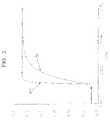
- FIG, 3is a comparative graph illustrating a signal edge rise-time from the output of the present invention versus the signal edge rise-time from a signal passed through a conventional multiplexer;
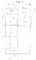
- FIG. 4is a block diagram of a high-speed multiplexer according to a second form of the present invention.
- a semiconductor tester 10is shown coupled to a handling apparatus 12 that includes a device interface board (DIB) 14 .
- the testerincludes a testhead (not shown) that houses a plurality of pin electronics channel cards 18 for generating tester waveforms along a plurality of channels 20 .
- the channelsdirect the waveforms to the input pins of one or more DUTs (not shown), and receive output waveforms from the DUT(s).
- the DIBincludes one or more sockets 22 for electrically coupling the DUT pins to the tester channels, thereby providing a convenient tester-to-DUT signal interface.
- selecting one channel 20 from a group of channelsis accomplished through use of a high-speed digital multiplexer, generally designated 30 .
- the multiplexerincludes a plurality of input pins 32 for receiving input signals from the channels, and switching circuitry 40 for activating one of the channels.
- a local signal converter in the form of a current-to-voltage converter 50detects the input pin current and converts it into a voltage, generating an output signal with rising and falling edges corresponding to the detected input signal edges.
- the ATE channels 20each include respective drivers 24 that respond to waveform formatting circuits (not shown) to generate digital test signals.
- the signalspropagate along cables that serve as transmission lines 26 that are impedance matched at 50 ohms. Because of the high frequencies envisioned (ranging from one gigahertz to five gigahertz), basic RF transmission line theory is applicable.
- the channels 20terminate on the multiplexer input pins 32 , which provide an interface to the multiplexer switching circuitry 40 .
- the switching circuitryincludes a plurality of semiconductor switches 42 , such as diodes or transistors, to activate a selected channel. In the embodiment shown in FIG. 2 , reverse-biased diodes are employed to sense the voltage levels applied to each channel.
- the activated channelis the one having the tester signal pulse, identified by Vt, applied to the channel. All the other channels having levels raised to a high voltage Vh.
- the diodesare disposed in parallel and are terminated on a common node 60 within the multiplexer. The node, in turn, connects to the local signal converter 50 .
- the local signal converter 50is, in a preferred form, a transresistance amplifier including a bipolar-junction-transistor (BJT) with a constant voltage Vb applied to the base, and having an emitter tied to the common node 60 .
- An output pathcouples to the BJT collector to define the multiplexer output OUT.
- Source voltage Vcc and resistor R 1bias the current source. In this manner, the transresistance amplifier acts as a current controlled voltage source.
- a userselects a particular channel 20 by programming the ATE 10 to drive all but the desired channel to the logical high voltage Vh.
- the base-to-emitter voltage Vb-Ve from the local signal converter 50sets the common node 60 to a constant voltage.
- the voltage Vb-Vewill be higher than the tester signal logic “one” (plus Vdiode), to activate the selected channel, but slightly lower than Vh to keep the rest of the diodes reversed-biased.
- the voltagewill be Vb-Ve-Vdiode. This is a constant voltage.
- both pointsact as RF short circuits, as is well known in the art.
- the input voltage signalshorts to an “AC” ground.
- the current flowing through the input pinchanges its value, corresponding to the energy exchange between the incoming pulse and the virtual “AC” short behavior of the input pin.
- These current changescause a corresponding increase in the voltage drop across R 1 , thereby generating a negative pulse with falling and rising edges at the output OUT, corresponding to the edges of the tester input signal.
- the pulse edges at the output OUTare delayed somewhat from the original tester input signal, this delay is the same for any selected channel, thus it is easily correctable through calibration procedures.
- the real benefitis in having an output signal unexposed to any RC effects from within the multiplexer 30 . As described above in detail, this is accomplished by keeping the common node 60 at a constant voltage, thus eliminating the effect of potential RC time constants from charging parasitic capacitances acting on the signal edges.
- FIG. 3illustrates comparative output waveforms from a conventional digital multiplexer at 70 , and an output signal according to the present invention, at 80 . Note that the waveform at 80 was first scaled to more easily illustrate the comparison. As shown in the graphs, by avoiding the parasitic RC's present on the common node 60 , a rise-time improvement on the order of a factor of eight (171 picoseconds versus 1319 picoseconds) is realized.
- FIG. 4illustrates the present invention according to a second form, generally designated 100 , which is more widely applicable to ATE and non-ATE applications alike.
- the constructionincludes a plurality of input pins 102 and switching circuitry 110 coupled to a local signal converter 120 .
- the difference in the second embodiment from the first embodimentlies primarily in the switching circuitry, which doesn't rely on the ATE to assist in the channel selection. Rather, a plurality of selection input bits 112 are provided to digitally identify a selected channel.
- the switching circuitryincludes a reverse-biased diode 114 that couples to an input pin buffer 116 .
- a semiconductor switch 118which acts to place the diode-to-buffer node, at 119 , at the supply voltage Vcc.
Landscapes
- Engineering & Computer Science (AREA)
- General Engineering & Computer Science (AREA)
- Physics & Mathematics (AREA)
- General Physics & Mathematics (AREA)
- Computer Networks & Wireless Communication (AREA)
- Tests Of Electronic Circuits (AREA)
- Analogue/Digital Conversion (AREA)
- Electronic Switches (AREA)
Abstract
Description
Claims (15)
Priority Applications (1)
| Application Number | Priority Date | Filing Date | Title |
|---|---|---|---|
| US11/671,105US7509227B2 (en) | 2001-11-08 | 2007-02-05 | High-speed digital multiplexer |
Applications Claiming Priority (2)
| Application Number | Priority Date | Filing Date | Title |
|---|---|---|---|
| US10/010,547US7222041B2 (en) | 2001-11-08 | 2001-11-08 | High-speed digital multiplexer |
| US11/671,105US7509227B2 (en) | 2001-11-08 | 2007-02-05 | High-speed digital multiplexer |
Related Parent Applications (1)
| Application Number | Title | Priority Date | Filing Date |
|---|---|---|---|
| US10/010,547DivisionUS7222041B2 (en) | 2001-11-08 | 2001-11-08 | High-speed digital multiplexer |
Publications (2)
| Publication Number | Publication Date |
|---|---|
| US20070146183A1 US20070146183A1 (en) | 2007-06-28 |
| US7509227B2true US7509227B2 (en) | 2009-03-24 |
Family
ID=21746259
Family Applications (2)
| Application Number | Title | Priority Date | Filing Date |
|---|---|---|---|
| US10/010,547Expired - Fee RelatedUS7222041B2 (en) | 2001-11-08 | 2001-11-08 | High-speed digital multiplexer |
| US11/671,105Expired - Fee RelatedUS7509227B2 (en) | 2001-11-08 | 2007-02-05 | High-speed digital multiplexer |
Family Applications Before (1)
| Application Number | Title | Priority Date | Filing Date |
|---|---|---|---|
| US10/010,547Expired - Fee RelatedUS7222041B2 (en) | 2001-11-08 | 2001-11-08 | High-speed digital multiplexer |
Country Status (1)
| Country | Link |
|---|---|
| US (2) | US7222041B2 (en) |
Families Citing this family (8)
| Publication number | Priority date | Publication date | Assignee | Title |
|---|---|---|---|---|
| WO2003071297A1 (en)* | 2002-02-15 | 2003-08-28 | Npt Est, Inc. | Signal paths providing multiple test configurations |
| DE102005055951A1 (en)* | 2005-11-24 | 2007-05-31 | Robert Bosch Gmbh | Evaluation circuit for processing digital signal, has signal paths and set of parameters assigned to each path, where different processing of input data item leads to processed data items that are dependent on parameters of respective paths |
| DE112007001595T5 (en)* | 2006-06-30 | 2009-07-30 | Teradyne, Inc., North Reading | calibration device |
| US7987063B2 (en) | 2008-04-22 | 2011-07-26 | Teradyne, Inc. | Fast, low power formatter for automatic test system |
| KR101394778B1 (en)* | 2010-01-20 | 2014-05-15 | 어드밴테스트 (싱가포르) 피티이. 엘티디. | Method and apparatus for testing a device-under-test |
| US11442098B2 (en)* | 2019-06-20 | 2022-09-13 | Teradyne, Inc. | Generating a waveform based on digital pulses |
| KR102853510B1 (en) | 2021-04-28 | 2025-09-02 | 주식회사 아도반테스토 | Circuit and method for calibrating multiple automatic test equipment channels |
| CN120142745A (en)* | 2025-05-15 | 2025-06-13 | 电子科技大学 | A multi-channel weak current time-sharing detection system |
Citations (6)
| Publication number | Priority date | Publication date | Assignee | Title |
|---|---|---|---|---|
| US5761208A (en)* | 1992-11-23 | 1998-06-02 | Brooktree Corporation | Expansible high speed digital multiplexer |
| US5959871A (en) | 1993-12-23 | 1999-09-28 | Analogix/Portland State University | Programmable analog array circuit |
| US6040732A (en)* | 1997-04-09 | 2000-03-21 | Analog Devices, Inc. | Switched-transconductance circuit within integrated T-switches |
| US6272669B1 (en) | 1997-12-15 | 2001-08-07 | Motorola, Inc. | Method for configuring a programmable semiconductor device |
| US20020048826A1 (en) | 1999-07-14 | 2002-04-25 | Richmond Donald Paul | Wafer level burn-in and electrical test system and method |
| US6535766B1 (en) | 2000-08-26 | 2003-03-18 | Medtronic, Inc. | Implanted medical device telemetry using integrated microelectromechanical filtering |
- 2001
- 2001-11-08USUS10/010,547patent/US7222041B2/ennot_activeExpired - Fee Related
- 2007
- 2007-02-05USUS11/671,105patent/US7509227B2/ennot_activeExpired - Fee Related
Patent Citations (6)
| Publication number | Priority date | Publication date | Assignee | Title |
|---|---|---|---|---|
| US5761208A (en)* | 1992-11-23 | 1998-06-02 | Brooktree Corporation | Expansible high speed digital multiplexer |
| US5959871A (en) | 1993-12-23 | 1999-09-28 | Analogix/Portland State University | Programmable analog array circuit |
| US6040732A (en)* | 1997-04-09 | 2000-03-21 | Analog Devices, Inc. | Switched-transconductance circuit within integrated T-switches |
| US6272669B1 (en) | 1997-12-15 | 2001-08-07 | Motorola, Inc. | Method for configuring a programmable semiconductor device |
| US20020048826A1 (en) | 1999-07-14 | 2002-04-25 | Richmond Donald Paul | Wafer level burn-in and electrical test system and method |
| US6535766B1 (en) | 2000-08-26 | 2003-03-18 | Medtronic, Inc. | Implanted medical device telemetry using integrated microelectromechanical filtering |
Also Published As
| Publication number | Publication date |
|---|---|
| US20070146183A1 (en) | 2007-06-28 |
| US7222041B2 (en) | 2007-05-22 |
| US20030086376A1 (en) | 2003-05-08 |
Similar Documents
| Publication | Publication Date | Title |
|---|---|---|
| US7509227B2 (en) | High-speed digital multiplexer | |
| US6275023B1 (en) | Semiconductor device tester and method for testing semiconductor device | |
| US6051979A (en) | System and method for detecting shorts, opens and connected pins on a printed circuit board using automatic test equipment | |
| US7019547B2 (en) | Pin driver for AC and DC semiconductor device testing | |
| US6879175B2 (en) | Hybrid AC/DC-coupled channel for automatic test equipment | |
| US6337573B1 (en) | Contact test circuit | |
| CN100504974C (en) | Driver circuit for display device | |
| EP0366553B1 (en) | Test device and method for testing electronic device and semiconductor device having the test device | |
| US5521493A (en) | Semiconductor test system including a novel driver/load circuit | |
| KR19990082339A (en) | Assemblies and Methods for Testing Integrated Circuit Devices | |
| JPH05232171A (en) | Transmission-line terminating apparatus | |
| JPH07151833A (en) | Driver circuit for integrated circuit tester | |
| US5696773A (en) | Apparatus for performing logic and leakage current tests on a digital logic circuit | |
| US6292010B1 (en) | Dynamic pin driver combining high voltage mode and high speed mode | |
| US7679390B2 (en) | Test apparatus and pin electronics card | |
| US7409615B2 (en) | Test apparatus and test method | |
| US6211723B1 (en) | Programmable load circuit for use in automatic test equipment | |
| US6621321B2 (en) | Circuit for conditioning output waveform | |
| US5826004A (en) | Input/output device with self-test capability in an integrated circuit | |
| US4879661A (en) | Bi-directional circuit to interface between a low current device and high current tester | |
| US6313669B1 (en) | Buffer circuitry | |
| US6373260B1 (en) | Single cable, single point, stimulus and response probing system and method | |
| KR100668250B1 (en) | Tristate Circuit and Method for Switching Output Signal Level | |
| JPH06148276A (en) | Semiconductor testing device and methopd | |
| JPH05312910A (en) | Semiconductor testing apparatus |
Legal Events
| Date | Code | Title | Description |
|---|---|---|---|
| AS | Assignment | Owner name:TERADYNE, INC., MASSACHUSETTS Free format text:ASSIGNMENT OF ASSIGNORS INTEREST;ASSIGNOR:IORGA, COSMIN;REEL/FRAME:018852/0314 Effective date:20011108 | |
| AS | Assignment | Owner name:BANK OF AMERICA, N.A., AS ADMINISTRATIVE AGENT, TE Free format text:NOTICE OF GRANT OF SECURITY INTEREST IN PATENTS;ASSIGNOR:TERADYNE, INC.;REEL/FRAME:021912/0762 Effective date:20081114 Owner name:BANK OF AMERICA, N.A., AS ADMINISTRATIVE AGENT,TEX Free format text:NOTICE OF GRANT OF SECURITY INTEREST IN PATENTS;ASSIGNOR:TERADYNE, INC.;REEL/FRAME:021912/0762 Effective date:20081114 | |
| FEPP | Fee payment procedure | Free format text:PAYOR NUMBER ASSIGNED (ORIGINAL EVENT CODE: ASPN); ENTITY STATUS OF PATENT OWNER: LARGE ENTITY | |
| STCF | Information on status: patent grant | Free format text:PATENTED CASE | |
| AS | Assignment | Owner name:TERADYNE, INC, MASSACHUSETTS Free format text:RELEASE BY SECURED PARTY;ASSIGNOR:BANK OF AMERICA, N.A.;REEL/FRAME:022668/0750 Effective date:20090427 Owner name:TERADYNE, INC,MASSACHUSETTS Free format text:RELEASE BY SECURED PARTY;ASSIGNOR:BANK OF AMERICA, N.A.;REEL/FRAME:022668/0750 Effective date:20090427 | |
| FPAY | Fee payment | Year of fee payment:4 | |
| AS | Assignment | Owner name:BARCLAYS BANK PLC, NEW YORK Free format text:PATENT SECURITY AGREEMENT;ASSIGNORS:TERADYNE, INC.;LITEPOINT CORPORATION;REEL/FRAME:035507/0116 Effective date:20150427 | |
| FPAY | Fee payment | Year of fee payment:8 | |
| AS | Assignment | Owner name:EAGLE TEST SYSTEMS, INC., ILLINOIS Free format text:RELEASE OF SECURITY INTEREST IN INTELLECTUAL PROPERTY;ASSIGNOR:BARCLAYS BANK PLC, AS COLLATERAL AGENT;REEL/FRAME:049632/0940 Effective date:20190627 Owner name:GENRAD, LLC, MASSACHUSETTS Free format text:RELEASE OF SECURITY INTEREST IN INTELLECTUAL PROPERTY;ASSIGNOR:BARCLAYS BANK PLC, AS COLLATERAL AGENT;REEL/FRAME:049632/0940 Effective date:20190627 Owner name:TERADYNE, INC., MASSACHUSETTS Free format text:RELEASE OF SECURITY INTEREST IN INTELLECTUAL PROPERTY;ASSIGNOR:BARCLAYS BANK PLC, AS COLLATERAL AGENT;REEL/FRAME:049632/0940 Effective date:20190627 Owner name:ENERGID TECHNOLOGIES CORPORATION, MASSACHUSETTS Free format text:RELEASE OF SECURITY INTEREST IN INTELLECTUAL PROPERTY;ASSIGNOR:BARCLAYS BANK PLC, AS COLLATERAL AGENT;REEL/FRAME:049632/0940 Effective date:20190627 Owner name:NEXTEST SYSTEMS CORPORATION, CALIFORNIA Free format text:RELEASE OF SECURITY INTEREST IN INTELLECTUAL PROPERTY;ASSIGNOR:BARCLAYS BANK PLC, AS COLLATERAL AGENT;REEL/FRAME:049632/0940 Effective date:20190627 Owner name:LITEPOINT CORPORATION, CALIFORNIA Free format text:RELEASE OF SECURITY INTEREST IN INTELLECTUAL PROPERTY;ASSIGNOR:BARCLAYS BANK PLC, AS COLLATERAL AGENT;REEL/FRAME:049632/0940 Effective date:20190627 | |
| AS | Assignment | Owner name:TRUIST BANK, GEORGIA Free format text:SECURITY INTEREST;ASSIGNOR:TERADYNE, INC.;REEL/FRAME:052595/0632 Effective date:20200501 | |
| FEPP | Fee payment procedure | Free format text:MAINTENANCE FEE REMINDER MAILED (ORIGINAL EVENT CODE: REM.); ENTITY STATUS OF PATENT OWNER: LARGE ENTITY | |
| LAPS | Lapse for failure to pay maintenance fees | Free format text:PATENT EXPIRED FOR FAILURE TO PAY MAINTENANCE FEES (ORIGINAL EVENT CODE: EXP.); ENTITY STATUS OF PATENT OWNER: LARGE ENTITY | |
| STCH | Information on status: patent discontinuation | Free format text:PATENT EXPIRED DUE TO NONPAYMENT OF MAINTENANCE FEES UNDER 37 CFR 1.362 | |
| FP | Lapsed due to failure to pay maintenance fee | Effective date:20210324 |