US7508715B2 - Coarse/fine program verification in non-volatile memory using different reference levels for improved sensing - Google Patents
Coarse/fine program verification in non-volatile memory using different reference levels for improved sensingDownload PDFInfo
- Publication number
- US7508715B2 US7508715B2US11/773,032US77303207AUS7508715B2US 7508715 B2US7508715 B2US 7508715B2US 77303207 AUS77303207 AUS 77303207AUS 7508715 B2US7508715 B2US 7508715B2
- Authority
- US
- United States
- Prior art keywords
- voltage
- bit line
- programming
- verify
- storage element
- Prior art date
- Legal status (The legal status is an assumption and is not a legal conclusion. Google has not performed a legal analysis and makes no representation as to the accuracy of the status listed.)
- Active
Links
Images


Classifications
- G—PHYSICS
- G11—INFORMATION STORAGE
- G11C—STATIC STORES
- G11C11/00—Digital stores characterised by the use of particular electric or magnetic storage elements; Storage elements therefor
- G11C11/56—Digital stores characterised by the use of particular electric or magnetic storage elements; Storage elements therefor using storage elements with more than two stable states represented by steps, e.g. of voltage, current, phase, frequency
- G11C11/5621—Digital stores characterised by the use of particular electric or magnetic storage elements; Storage elements therefor using storage elements with more than two stable states represented by steps, e.g. of voltage, current, phase, frequency using charge storage in a floating gate
- G11C11/5628—Programming or writing circuits; Data input circuits
- G—PHYSICS
- G11—INFORMATION STORAGE
- G11C—STATIC STORES
- G11C16/00—Erasable programmable read-only memories
- G11C16/02—Erasable programmable read-only memories electrically programmable
- G11C16/04—Erasable programmable read-only memories electrically programmable using variable threshold transistors, e.g. FAMOS
- G11C16/0483—Erasable programmable read-only memories electrically programmable using variable threshold transistors, e.g. FAMOS comprising cells having several storage transistors connected in series
- G—PHYSICS
- G11—INFORMATION STORAGE
- G11C—STATIC STORES
- G11C2211/00—Indexing scheme relating to digital stores characterized by the use of particular electric or magnetic storage elements; Storage elements therefor
- G11C2211/56—Indexing scheme relating to G11C11/56 and sub-groups for features not covered by these groups
- G11C2211/562—Multilevel memory programming aspects
- G11C2211/5621—Multilevel programming verification
- G—PHYSICS
- G11—INFORMATION STORAGE
- G11C—STATIC STORES
- G11C2211/00—Indexing scheme relating to digital stores characterized by the use of particular electric or magnetic storage elements; Storage elements therefor
- G11C2211/56—Indexing scheme relating to G11C11/56 and sub-groups for features not covered by these groups
- G11C2211/563—Multilevel memory reading aspects
- G11C2211/5634—Reference cells
Definitions
- the present disclosurerelates to programming in non-volatile memory.
- Non-volatile semiconductor memory deviceshave become more popular for use in various electronic devices.
- non-volatile semiconductor memoryis used in cellular telephones, digital cameras, personal digital assistants, mobile computing devices, non-mobile computing devices and other devices.
- Electrical Erasable Programmable Read Only Memory (EEPROM), including flash EEPROM, and Electronically Programmable Read Only Memory (EPROM)are among the most popular non-volatile semiconductor memories.
- EEPROM and EPROM memoriesutilize a floating gate that is positioned above and insulated from a channel region in a semiconductor substrate.
- the floating gateis positioned between source and drain regions.
- a control gateis provided over and insulated from the floating gate.
- the threshold voltage of the transistoris controlled by the amount of charge that is retained on the floating gate.
- the minimum amount of voltage that must be applied to the control gate before the transistor is turned on to permit conduction between its source and drainis controlled by the level of charge on the floating gate.
- a program voltageis applied to the control gate and the bit line is grounded. Electrons from the channel are injected into the floating gate. When electrons accumulate in the floating gate, the floating gate becomes negatively charged and the threshold voltage of the memory cell is raised so that the memory cell is in the programmed state.
- FIG. 1shows a graph depicting two threshold voltage distributions.
- the x axisplots threshold voltage and the y axis plots the number of memory cells.
- the threshold voltages in distribution 2are less than zero volts.
- threshold voltage distribution 2corresponds to erased memory cells that store data “1.”
- the threshold voltages in distribution 4are greater than zero volts.
- threshold voltage distribution 4corresponds to programmed memory cells that store data “0.”
- a multi-state flash memory cellis implemented by identifying multiple, distinct allowed threshold voltage ranges separated by forbidden voltage ranges. Each distinct threshold voltage range corresponds to a predetermined value for the set of data bits.
- FIG. 2illustrates threshold voltage distributions for memory cells storing two bits of data through the use of four data states.
- threshold voltage distribution 2represents memory cells that are in the erased state (e.g., storing “11”), having negative threshold voltage levels.
- Threshold voltage distribution 10represents memory cells that store data “10,” having positive threshold voltage levels.
- Threshold voltage distribution 12represents memory cells storing data “00.”
- Threshold voltage distribution 14represents memory cells that are storing “01.” In some implementations (as exemplified above), these data values (e.g.
- each of the distributionscan correspond to different data states than described above.
- the specific relationship between the data programmed into the memory cell and the threshold voltage ranges of the celldepends upon the data encoding scheme adopted for the memory cells.
- Threshold voltage distributions 2 and 4show the erased and programmed voltage-distributions when no verify operations are used. These distributions can be obtained by programming or erasing the memory cells with one single programming or erase pulse. Depending on the memory array size and the variations in the production process, threshold voltage distribution 4 will have a certain width, known as the natural V th width.
- distributions 10 , 12 , and 14(corresponding to programming a multi-state device) need to be much narrower than the natural V th width of distribution 4 .
- a process that uses multiple programming pulses and verify operationssuch as that described by FIGS. 3A , 3 B, and 3 C, can be used.
- FIG. 3Adepicts a programming voltage signal V pgm that is applied to the control gate as a series of pulses.
- the magnitude of the pulseis increased with each successive pulse by a pre-determined step size (e.g., 0.2V-0.4V), depicted in FIG. 3A as ⁇ V pgm .
- verify operationsare carried out.
- the time-burdenis a more efficient verification process, such as the process that is disclosed in U.S. patent application Ser. No. 10/314,055 entitled, “Smart Verify For Multi-State Memories,” filed Dec. 5, 2002, incorporated herein by reference in its entirety.
- the pulses of FIG. 3Aare separated from each other by a time period during which verification is performed.
- the time period for verificationis omitted from the drawing.
- FIG. 3Bdepicts the voltage signal applied to a bit line for the associated memory cell being programmed.
- FIG. 3Cdepicts the threshold voltage of the memory cell being programmed. Note that the graph in FIG. 3C is smoothed out to make it easier to read.
- a verify operationis carried out (not shown.) During the verify operation, the threshold voltage of the memory cell to be programmed is checked. If the threshold voltage of the memory cell is larger than the target value (e.g., V verify ), then programming for that memory cell is inhibited in the next cycle by raising the bit line voltage from 0v to V inhibit (e.g., at time t 4 ).
- the target valuee.g., V verify
- the multiple ranges of threshold voltages of the multi-state memory cellsshould be separated from each other by sufficient margin so that the level of the memory cell can be programmed and read in an unambiguous manner.
- a tight threshold voltage distributionis recommended. To achieve a tight threshold voltage distribution, small program steps have typically been used, thereby programming the threshold voltage of the cells more slowly. The tighter the desired threshold voltage distribution the smaller the steps and the slower the programming process.
- One solution for achieving tight threshold voltage distributions, without unreasonably slowing down the programming processincludes using a two-phase programming process.
- the first phasea coarse programming phase, includes an attempt to raise a threshold voltage in a faster manner while paying less attention to achieving a tight threshold voltage distribution.
- the second phasea fine programming phase, attempts to raise the threshold voltage in a slower manner in order to reach the target threshold voltage, thus achieving a tighter threshold voltage distribution.
- a coarse/fine programming methodologycan be found in U.S. Pat. No. 6,643,188, incorporated herein by reference in its entirety.
- FIGS. 4 and 5provide more detail of one example of a coarse/fine programming methodology.
- FIGS. 4A and 5Adepict the programming pulses V pgm applied to the control gate.
- FIGS. 4B and 5Bdepict the bit line voltages for the memory cells being programmed.
- FIGS. 4C and 5Cdepict the threshold voltage of the memory cells being programmed.
- the example of FIGS. 4 and 5depicts programming of memory cells to state A using two verify levels, indicated in the Figures as V vA1 and V vA2 . The final target level is V vA2 .
- V vA2The final target level
- the memory cellwill be inhibited from further programming by applying an inhibit voltage to the bit line corresponding to that memory cell.
- the bit line voltagecan be raised to V inhibit (See FIG. 4B and FIG. 5B ).
- V inhibitSee FIG. 4B and FIG. 5B .
- the threshold voltage shift of the memory cell during subsequent programming pulsesis slowed down by applying a certain bias voltage to the bit line, typically on the order of 0.3V to 0.8V. Because the rate of threshold voltage shift is reduced during the next few programming pulses, the final threshold voltage distribution can be narrower than with the methods depicted in FIG. 3 .
- a second verify levelthat is lower than that of V vA2 is used. This second verify level is depicted in FIGS. 4 and 5 as V vA1 .
- the threshold voltage shift to the memory cellwill be reduced for subsequent programming pulses by applying a bit line bias V s ( FIG. 5B ).
- V sbit line bias
- two verify operationsare required for each state.
- Thismay increase the total time needed to program the memory cells.
- a larger ⁇ V pgm step sizecan be used to speed up the process.
- FIGS. 4A , 4 B, and 4 Cshow the behavior of a memory cell whose threshold voltage moves past V vA1 and V vA2 in one programming pulse.
- the threshold voltageis depicted in FIG. 4C to pass V vA1 and V vA2 in between t 2 and t 3 .
- the memory cellprior to t 3 , the memory cell is in the coarse phase. After t 3 , the memory cell is in the inhibit mode.
- FIGS. 5A , 5 B, and 5 Cdepict a memory cell that enters both the coarse and fine programming phases.
- the threshold voltage of the memory cellcrosses V vA1 in between time t 2 and time t 3 .
- the memory cellPrior to t 3 , the memory cell is in the coarse phase.
- the bit line voltageis raised to Vs to place the memory cell in the fine phase.
- the threshold voltage of the memory cellcrosses V vA2 . Therefore, the memory cell is inhibited from further programming by raising the bit line voltage to V inhibit .
- coarse/fine programming algorithmsare not applied to the highest memory state (the state corresponding to the largest positive threshold voltage range).
- the highest statesuch as state C represented by distribution 14 in FIG. 2
- state Cdoes not need to be differentiated from a higher state.
- state Brepresented by distribution 12
- the distribution of these cellscan occupy a wider threshold voltage range without adverse effects on device performance.
- some implementationswill make use of coarse/fine programming techniques when programming the highest level state as well.
- the technology described hereinattempts to provide a more accurate sensing of the threshold voltage of non-volatile storage elements during programming verification when coarse/fine programming is utilized.
- Coarse/fine programming of non-volatile memoryis provided in which memory cells are programmed at a first rate of programming prior to reaching a coarse verify level for their intended state and a second rate of programming after reaching the coarse verify level but before reaching the final verify level for their intended state.
- Large sub-threshold swing factors associated with smaller memory cellscan affect the accuracy of sense operations, particularly when sensing at a fine verify level after sensing at a coarse verify level without pre-charging the bit line between the different sensings.
- Different reference potentialsare utilized when sensing at a coarse verify level and a final verify level. The difference between the reference potentials can compensate for any discharge of the bit line during the coarse level sensing.
- One embodimentincludes a method of programming non-volatile memory.
- the methodincludes applying one or more programming pulses to a set of non-volatile storage elements to program one or more storage elements of the set to a particular state. After applying each programming pulse, programming of the one or more storage elements to an intermediate verify level corresponding to the particular state is verified by applying a first voltage to the set of storage elements and comparing a bit line voltage of each of the one or more storage elements to a first reference potential.
- verifying programming of the one or more storage elements to a final verify level corresponding to the particular stateis preformed by applying a second voltage to the set of storage elements and comparing the bit line voltage of each of the one or more storage elements to a second reference potential, the second reference potential compensates for a decrease in the bit line voltage of each of the one or more storage elements resulting from the verifying programming to the intermediate verify level.
- a method of verifying programming of non-volatile storageincludes charging a bit line corresponding to a non-volatile storage element, applying to the non-volatile storage element an intermediate verify voltage corresponding to a target state for the non-volatile storage element, sensing a voltage of the bit line while the intermediate verify voltage is applied, comparing the voltage of the bit line to a first reference potential, applying to the non-volatile storage element a final verify voltage corresponding to the target state for the non-volatile storage element, sensing the voltage of the bit line while the final verify voltage is applied and before the bit line completely discharges from the charging, and comparing the voltage of the bit line while the final verify voltage is applied to a second reference potential.
- One exemplary implementationincludes a set of non-volatile storage elements and one or more managing circuits in communication with the set of non-volatile storage elements.
- the one or more managing circuitscan perform the processes described above.
- FIG. 1is a graph depicting two threshold voltage distributions.
- FIG. 2is a graph depicting four threshold voltage distributions.
- FIGS. 3A , 3 B and 3 Cdepict a programming process.
- FIG. 3Adepicts a programming voltage signal that is applied to a control gate of a non-volatile storage element.
- FIG. 3Bdepicts a voltage signal applied to a bit line for a NAND string.
- FIG. 3Cdepicts the threshold voltage of the non-volatile storage element being programmed.
- FIGS. 4A , 4 B and 4 Cdepict one embodiment of a programming process that is performed as part of coarse/fine programming.
- FIGS. 5A , 5 B and 5 Cdepict one embodiment of a programming process that is performed as part of coarse/fine programming.
- FIG. 6is a top view of a NAND string.
- FIG. 7is an equivalent circuit diagram of the NAND string of FIG. 6 .
- FIG. 8is a block diagram of one embodiment of a non-volatile memory system.
- FIG. 9illustrates an example of an organization of a memory array.
- FIG. 10depicts a program voltage signal, including verify pulses, that can be used in accordance with one embodiment.
- FIG. 11is a flowchart describing a method of programming non-volatile memory in accordance with one embodiment.
- FIG. 12depicts an exemplary set of threshold voltage distributions and a full sequence programming process.
- FIG. 13depicts an exemplary set of threshold voltage distributions and a two-pass programming process.
- FIGS. 14A-14Cdepict an exemplary set of threshold voltage distributions and another two-pass programming process.
- FIG. 15is timing diagram describing various signals that may be applied to a memory device during a program and program verification operation.
- FIG. 16is a graph describing the bit line potential of different memory cells during a verification operation where the memory cells have small sub-threshold swing factors.
- FIG. 17is a graph describing the bit line potential of different memory cells during a verification operation where the memory cells have larger sub-threshold swing factors.
- FIG. 18is a graph describing the bit line potential of different memory cells during a verification process in accordance with one embodiment.
- FIG. 19is a flowchart describing verification of memory cells during coarse/fine programming in accordance with one embodiment.
- FIG. 20is a portion of the column control circuitry of a memory device that can be used in accordance with one embodiment.
- FIG. 6is a top view showing one NAND string.
- FIG. 7is an equivalent circuit thereof.
- the NAND string depicted in FIGS. 5 and 6includes four transistors 100 , 102 , 104 and 106 in series and sandwiched between a select gate 120 and a second select gate 122 .
- Select gate 120connects the NAND string to bit line contact 126 .
- Select gate 122connects the NAND string to source line contact 128 .
- Select gate 120is controlled by the applying appropriate voltages to control gate 120 CG.
- Select gate 122is controlled by applying the appropriate voltages to control gate 122 CG.
- Each of the transistors 100 , 102 , 104 and 106has a control gate and a floating gate.
- Transistor 100has control gate 100 CG and floating gate 100 FG.
- Transistor 102includes control gate 102 CG and floating gate 102 FG.
- Transistor 104includes control gate 104 CG and floating gate 104 FG.
- Transistor 106includes a control gate 106 CG and floating gate 106 FG.
- Control gate 100 CGis connected to word line WL 3
- control gate 102 CGis connected to word line WL 2
- control gate 104 CGis connected to word line WL 1
- control gate 106 CGis connected to word line WL 0 .
- transistors 100 , 102 , 104 and 106are each memory cells. In other embodiments, the memory cells may include multiple transistors or may be different than those depicted in FIGS. 6 and 7 .
- Select gate 120is connected to select line SGD, and select gate 122 is connected to select line SGS.
- FIGS. 6 and 7show four memory cells in the NAND string, the use of four transistors is only provided as an example.
- a NAND stringcan have less than four memory cells or more than four memory cells.
- some NAND stringswill include 8 memory cells, 16 memory cells, 32 memory cells, etc. The discussion herein is not limited to any particular number of memory cells in a NAND string.
- the technology described hereinis not limited to floating gate types of memory.
- the technology described hereincan be used with memory devices that use various types of charge storage regions/layer(s) between the control gate (or word line) and the substrate, such as a non-conductive dielectric charge storage region or small silicon islands, better known as nano-crystals.
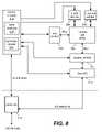
- FIG. 8is a block diagram of one embodiment of a flash memory system that can be used to implement one or more embodiments of the present disclosure.
- FIG. 8is exemplary as other systems and implementations can be used.
- Memory cell array 302is controlled by column control circuit 304 , row control circuit 306 , c-source control circuit 310 and p-well control circuit 308 .
- Column control circuit 304is connected to the bit lines of memory cell array 302 for reading data stored in the memory cells, for determining a state of the memory cells during a program operation, and for controlling potential levels of the bit lines to promote or inhibit programming and erasing.
- Row control circuit 306is connected to the word lines to select one of the word lines, to apply read voltages, to apply program voltages combined with the bit line potential levels controlled by column control circuit 304 , and to apply an erase voltage.
- C-source control circuit 310controls a common source line (labeled as “C-source” in FIG. 9 ) connected to the memory cells.
- P-well control circuit 308controls the p-well voltage.
- the data stored in the memory cellsare read out by the column control circuit 304 and are output to external I/O lines via data input/output buffer 312 .
- Program data to be stored in the memory cellsare input to the data input/output buffer 312 via the external I/O lines, and transferred to the column control circuit 304 .
- the external I/O linesare connected to controller 318 .
- Command data for controlling the flash memory deviceis input to controller 318 .
- the command datainforms the flash memory of what operation is requested.
- the input commandis transferred to state machine 316 which is part of control circuitry 315 .
- State machine 316can also output status data of the flash memory such as READY/BUSY or PASS/FAIL.
- Controller 318is connected to or connectable with a host system such as a personal computer, a digital camera, or personal digital assistant, etc. It communicates with the host that initiates commands, such as to store or read data to or from the memory array 302 , and provides or receives such data. Controller 318 converts such commands into command signals that can be interpreted and executed by command circuits 314 which are part of control circuitry 315 . Command circuits 314 are in communication with state machine 316 . Controller 318 typically contains buffer memory for the user data being written to or read from the memory array.
- One exemplary memory systemcomprises one integrated circuit that includes controller 318 , and one or more integrated circuit chips that each contain a memory array and associated control, input/output and state machine circuits.
- the memory systemmay be embedded as part of the host system, or may be included in a memory card (or other package) that is removably inserted into the host systems.
- a memory cardmay include the entire memory system (e.g. including the controller) or just the memory array(s) with associated peripheral circuits (with the controller or control function being embedded in the host).
- the controllercan be embedded in the host or included within the removable memory system.
- one or more of the components of FIG. 8can be combined.
- one or more of the components of FIG. 8can be thought of as managing circuitry for the memory system.
- one or more managing circuitsmay include any one of or a combination of a command circuit, a state machine, a row control circuit, a column control circuit, a well control circuit, a source control circuit, a data I/O circuit, or a controller.
- a NAND flash EEPROMis described that is partitioned into 1,024 blocks.
- the data stored in each blockis simultaneously erased.
- the blockis the minimum unit of cells that are simultaneously erased.
- Each blockis typically divided into a number of pages which can be a unit of programming. Other units of data for programming are also possible and contemplated.
- individual pagesmay be divided into segments and the segments may contain the fewest number of cells that are written at one time as a basic programming operation.
- One or more pages of dataare typically stored in one row of memory cells.
- each block of the example in FIG. 9there are 8,512 columns that are divided into even columns and odd columns.
- the bit linesare also divided into even bit lines (BLe) and odd bit lines (BLo).
- BLeeven bit lines
- BLoodd bit lines
- memory cells along a common word line and connected to the odd bit linesare programmed at one time, while memory cells along a common word line and connected to even bit lines are programmed at another time.
- four cellsare shown to be included in each NAND string in FIG. 9 , more or less than four memory cells can be used.
- One terminal of the NAND stringis connected to a corresponding bit line via a first select transistor that is connected to a drain select gate control line SGD, and another terminal is connected to C-source via a second select transistor that is connected to a source select gate control line SGS.
- bit linesare not divided into odd and even bit lines.
- Such architecturesare commonly referred to as all bit line architectures.
- all bit lines of a blockare simultaneously selected during read and program operations. Memory cells along a common word line and connected to any bit line are programmed at the same time.
- Memory cellsare erased by raising the p-well to an erase voltage (e.g. 20 volts) and grounding the word lines of a selected block.
- the source and bit linesare floating. Erasing can be performed on the entire memory array, separate blocks, or another unit of cells. Electrons are transferred from the floating gate to the p-well region and the threshold voltage becomes negative (in one embodiment).
- the drain and the p-wellreceive 0V while the control gate receives a series of programming pulses with increasing magnitudes.
- the magnitudes of the pulses in the seriesrange from 12V to 24V. In other embodiments, the range of pulses in the series can be different, for example, having a starting level of higher than 12V.
- verify operationsare carried out in the periods between the programming pulses. That is, the programming level of each cell of a group of cells being programmed in parallel is read between each programming pulse to determine whether or not it has reached or exceeded a verify level to which it is being programmed.
- One means of verifying the programmingis to test conduction at a specific compare point.
- the cells that are verified to be sufficiently programmedare locked out, for example in NAND cells, by raising the bit line voltage from 0 to V DD (e.g., 2.5V) for all subsequent programming pulses to terminate the programming process for those cells.
- V DDe.g. 2.5V
- the number of pulseswill be limited (e.g. 20 pulses) and if a given memory cell is not sufficiently programmed by the last pulse, an error is assumed.
- memory cellsare erased (in blocks or other units) prior to programming.
- FIG. 10depicts a program voltage signal in accordance with one embodiment.
- This signalhas a set of pulses with increasing magnitudes. The magnitude is increased with each pulse by a predetermined step size. In one embodiment that includes the memory cells storing multiple bits of data, an exemplary step size is 0.2V (or 0.4V).
- an exemplary step sizeis 0.2V (or 0.4V).
- the signal of FIG. 10assumes a four state memory cell, therefore, it includes three verify pulses. For example, between programming pulses 330 and 332 are three sequential verify pulses.
- the first verify pulse 334is depicted at a zero volt verify voltage level.
- the second verify pulse 336follows the first verify pulse at the second verify voltage level.
- the third verify pulse 338follows the second verify pulse 336 at the third verify voltage level.
- a multi-state memory cell capable of storing data in eight statesmay need to perform verify operations at seven compare points.
- seven verify pulsesare applied in sequence to perform seven verify operations at seven verify levels between two consecutive programming pulses.
- the systemcan determine the state of the memory cells.
- One means for reducing the time burden of verifyingis to use a more efficient verify process, for example, as disclosed in: U.S. patent application Ser. No. 10/314,055, entitled “Smart Verify for Multi-State Memories,” filed Dec. 5, 2002; U.S. patent application Ser. No. 11/259,799, entitled “Method for Programming of Multi-State Non-Volatile Memory Using Smart Verify, filed Oct. 27, 2005; and U.S. patent application Ser. No. 11/260,658, entitled “Apparatus for Programming of Multi-State Non-Volatile Memory Using Smart Verify,” filed Oct. 27, 2005, all of which are incorporated herein by reference in their entirety.
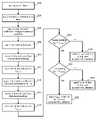
- FIG. 11is a flow chart describing one embodiment of a method for programming non-volatile memory.
- the memory cells to be programmedare erased at step 340 .
- Step 340can include erasing more memory cells than those to be programmed (e.g., in blocks or other units).
- soft programmingis performed to narrow the distribution of erased threshold voltages for the erased memory cells. Some memory cells may be in a deeper erased state than necessary as a result of the erase process. Soft programming can apply small programming pulses to move the threshold voltage of the erased memory cells closer to the erase verify level.
- Soft programmingcan apply small programming pulses to move the threshold voltage of the erased memory cells closer to the erase verify level.
- a “data load” commandis issued by controller 318 and input to command circuits 314 , allowing data to be input to data input/output buffer 312 .
- the input datais recognized as a command and latched by state machine 316 via a command latch signal, not illustrated, input to command circuits 314 .
- address data designating the page addressis input to row controller or decoder 306 from the controller or host.
- the input datais recognized as the page address and latched via state machine 316 , affected by the address latch signal input to command circuits 314 .
- a page of program data for the addressed pageis input to data input/output buffer 312 for programming. For example, 532 bytes of data could be input in one embodiment.
- That datais latched in the appropriate registers for the selected bit lines. In some embodiments, the data is also latched in a second register for the selected bit lines to be used for verify operations.
- a “program” commandis issued by the controller and input to data input/output buffer 312 . The command is latched by state machine 316 via the command latch signal input to command circuits 314 .
- V pgmthe programming pulse voltage level applied to the selected word line, is initialized to the starting pulse (e.g., 12V) and a program counter PC maintained by state machine 316 is initialized at 0.
- the first V pgm pulseis applied to the selected word line. If logic “0” is stored in a particular data latch indicating that the corresponding memory cell should be programmed, then the corresponding bit line is grounded. On the other hand, if logic “1” is stored in the particular latch indicating that the corresponding memory cell should remain in its current data state, then the corresponding bit line is connected to V DD to inhibit programming.
- the states of the selected memory cellsare verified. If it is detected that the target threshold voltage of a selected cell has reached the appropriate level, then the data stored in the corresponding data latch is changed to a logic “1.” If it is detected that the threshold voltage has not reached the appropriate level, the data stored in the corresponding data latch is not changed. In this manner, a bit line having a logic “1” stored in its corresponding data latch does not need to be programmed. When all of the data latches are storing logic “1,” the state machine knows that all selected cells have been programmed. At step 364 , it is checked whether all of the data latches are storing logic “1.” If so, the programming process is complete and successful because all selected memory cells were programmed and verified to their target states. A status of “PASS” is reported at step 366 .
- the programming processcontinues.
- the program counter PCis checked against a program limit value.
- a program limit valueis 20, however, other values can be used in various implementations. If the program counter PC is not less than 20, then it is determined at step 369 whether the number of bits that have not been successfully programmed is equal to or less than a predetermined number. If the number of unsuccessfully programmed bits is equal to or less than the predetermined number, then the programming process is flagged as passed and a status of pass is reported at step 371 . The bits that are not successfully programmed can be corrected using error correction during the read process.
- step 370If however, the number of unsuccessfully programmed bits is greater than the predetermined number, the program process is flagged as failed and a status of fail is reported at step 370 . If the program counter PC is less than 20, then the V pgm level is increased by the step size and the program counter PC is incremented at step 372 . After step 372 , the process loops back to step 360 to apply the next V pgm pulse.
- the threshold voltages of the memory cellsshould be within one or more distributions of threshold voltages for programmed memory cells or within a distribution of threshold voltages for erased memory cells, as appropriate.
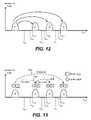
- FIG. 12illustrates threshold voltage distributions for the memory cell array when each memory cell stores two bits of data.
- FIG. 12shows a first threshold voltage distribution E for erased memory cells. Three threshold voltage distributions, A, B and C for programmed memory cells, are also depicted. In one embodiment, the threshold voltages in the E distribution are negative and the threshold voltages in the A, B and C distributions are positive.
- Each distinct threshold voltage range of FIG. 12corresponds to predetermined values for the set of data bits.
- the specific relationship between the data programmed into the memory cell and the threshold voltage levels of the celldepends upon the data encoding scheme adopted for the cells.
- data valuesare assigned to the threshold voltage ranges using a gray code assignment so that if the threshold voltage of a floating gate erroneously shifts to its neighboring physical state, only one bit will be affected.
- gray codingis not used.
- One exampleassigns “11” to threshold voltage range E (state E), “10” to threshold voltage range A (state A), “00” to threshold voltage range B (state B) and “01” to threshold voltage range C (state C).
- FIG. 12shows four states, embodiments in accordance of the present disclosure can include other multi-state structures including those that include more or less than four states.
- FIG. 12also depicts an embodiment that utilizes full sequence programming.
- full sequence programmingmemory cells can be programmed from the erase state E directly to any of the programmed states A, B or C.
- a population of memory cells to be programmedmay first be erased so that all memory cells in the population are in erased state E.
- the process described in FIG. 11 using a series of program voltage pulses applied to the control gates of selected memory cellswill be used to program the memory cells directly into states A, B or C. While some memory cells are being programmed from state E to state A, other memory cells are being programmed from state E to state B and/or from state E to state C.
- FIG. 13illustrates an example of a two-pass technique of programming a multi-state memory cell that stores data for two different pages: a lower page and an upper page.
- statesare depicted: state E (11), state A (10), state B (00) and state C (01).
- state Eboth pages store a “1.”
- state Athe lower page stores a “0” and the upper page stores a “1.”
- state Bboth pages store “0.”
- state Cthe lower page stores “1” and the upper page stores “0.”
- bit patternsmay also be assigned.
- the cell's threshold voltage levelis set according to the bit to be programmed into the lower logical page.
- the threshold voltageis not changed since it is in the appropriate state as a result of having been earlier erased. However, if the bit to be programmed is logic “0,” the threshold level of the cell is increased to be state A, as shown by arrow 402 . That concludes the first programming pass.
- the cell's threshold voltage levelis set according to the bit being programmed into the upper logical page. If the upper logical page bit is to store a logic “1,” then no programming occurs since the cell is in one of the states E or A, depending upon the programming of the lower page bit, both of which carry an upper page bit of “1.” If the upper page bit is to be logic “0,” then the threshold voltage is shifted. If the first pass resulted in the cell remaining in the erased state E, then in the second phase the cell is programmed so that the threshold voltage is increased to be within state C, as depicted by arrow 406 .
- the memory cellis further programmed in the second pass so that the threshold voltage is increased to be within state B, as depicted by arrow 404 .
- the result of the second passis to program the cell into the state designated to store logic “0” for the upper page without changing the data for the lower page.
- Steps 358 - 372may be performed for each pass of the programming operation.
- one or more program pulsesmay be applied and the results thereof verified to determine if a cell is in the appropriate intermediate state.
- one or more program pulsesmay be applied and the results thereof verified to determine if the cell is in the appropriate final state.
- this techniquemay include separate data load and program commands as well as separate inputs of address and program data as shown in steps 350 - 356 .
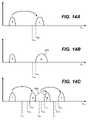
- FIGS. 14A-14Cdisclose another process for programming non-volatile memory that reduces floating gate to floating gate coupling, for any particular memory cell, by writing to that particular memory cell with respect to a particular page subsequent to writing to adjacent memory cells for previous pages.
- the non-volatile memory cellsstore two bits of data per memory cell, using four data states. For example, assume that state E is the erased state and states A, B and C are the programmed states. State E stores data 11 . State A stores data 01 . State B stores data 10 . State C stores data 00 . Other encodings of data to physical data states can also be used. Each memory cell stores two pages of data.
- FIGS. 14A-14Care two-step processes. In the first step, the lower page is programmed. If the lower page is to remain data 1 , then the memory cell state remains at state E. If the data is to be programmed to 0, then the threshold of voltage of the memory cell is raised such that the memory cell is programmed to interim state B′.
- FIG. 14Bshows the programming of memory cells from state E to state B′. State B′ depicted in FIG. 14A is an interim state B′. Therefore, the verify point is depicted as V vB ′, which is lower than V vB .
- a memory cellafter a memory cell is programmed from state E to state B, its neighbor memory cell in the NAND string will then be programmed with respect to its lower page. For example, looking back at FIG. 7 , after the lower page for memory cell 106 is programmed, the lower page for memory cell 104 would be programmed.
- the floating gate to floating gate coupling effectwill raise the apparent threshold voltage of memory cell 106 if memory cell 104 had a threshold voltage raised from state E to state B. This will have the effect of widening the threshold voltage distribution for state B to that depicted as threshold voltage distribution 320 of FIG. 14B . This apparent widening of the threshold voltage distribution will be remedied when programming the upper page.
- FIG. 14Cdepicts the process of programming the upper page. If the memory cell is in erased state E and the upper page is to remain at 1, then the memory cell will remain in state E. If the memory cell is in state E and its upper page data is to be programmed to 0, then the threshold voltage of the memory cell will be raised so that the memory cell is in state A. If the memory cell was in intermediate threshold voltage distribution 320 and the upper page data is to remain at 1, then the memory cell will be programmed to final state B. If the memory cell is in intermediate threshold voltage distribution 320 and the upper page data is to become data 0 , then the threshold voltage of the memory cell will be raised so that the memory cell is in state C.
- the process depicted by FIGS. 14A-14Creduces the effect of floating gate to floating gate coupling because only the upper page programming of neighboring memory cells will have an effect on the apparent threshold voltage of a given memory cell.
- FIGS. 14A-14Cprovide an example with respect to four data states and two pages of data, the concepts taught by FIGS. 14A-14C can be applied to other implementations with more or less than four states and different numbers of pages.
- FIGS. 12 , 13 and 14 A- 14 Cshow read reference voltages, V rA , V rB and V rC for reading data from memory cells.
- V cgapplied control gate voltage
- the select gates of a selected blockare raised to one or more select voltages and the unselected word lines (e.g., WL 0 , WL 2 and WL 3 ) are raised to a read pass voltage V read (e.g. 4.5 volts) to make the transistors operate as pass gates.
- V reade.g. 4.5 volts
- the source and p-wellare at zero volts.
- the selected bit lines (BLe)are pre-charged to a level of, for example, 0.7V.
- the selected word line(e.g. WL 1 ) is connected to a read or verify voltage, a level of which is specified for each read and verify operation in order to determine whether a threshold voltage of the concerned memory cell is above or below such level.
- the threshold voltageis higher than the read or verify level on the word line, the potential level of the bit line (BLe) associated with the cell of interest maintains the high level because of the non-conductive memory cell.
- the threshold voltageis lower than the read or verify level, the potential level of the concerned bit line (BLe) decreases to a low level, for example less than 0.5V, because of the conductive memory cell discharging the bitline.
- the state of the memory cellis thereby detected by a voltage comparator sense amplifier that is connected to the bit line to sense the resulting bit line voltage.
- FIGS. 12 , 13 and 14 A- 14 Calso show verify voltages including V vA2 , V vB2 and V vC2 .
- V vA2threshold voltage greater than or equal to V vA2
- V vB2threshold voltage greater than or equal to V vC2
- FIGS. 12 , 13 and 14 A- 14 Calso show verify voltages including V vA2 , V vB2 and V vC2 .
- coarse/fine programminguses two sets of verify voltages for one or more of the programmable states to both verify the final level of programming for a memory cell and additionally, to switch cells from the coarse programming phase to the fine programming phase when the cell has become close to, but has not yet reached the final verify level for its intended state.
- FIGS. 12 , 13 and 14 A- 14 Ctwo sets of verify levels are depicted for each programmed state. Verify levels V vA1 , V vB1 and V vC1 are used to verify that a memory cell has reached the coarse verify level while verify levels V vA2 , V vB2 and V vC2 are used to verify that a memory cell has reached the final verify level for its intended state.
- FIG. 15is a timing diagram depicting various signals that are applied to a non-volatile memory device during part of an exemplary programming process that includes coarse ⁇ fine programming.
- the first period of time labeled “programming”includes the signals that are applied to program one or more memory cells of a selected word line WL_sel.
- This programming periodis generalized and as such, might correspond to the first programming pulse applied to the word line or a second or later programming pulse. This period corresponds to step 360 in FIG. 11 .
- the programming periodbegins by raising the source line to a low positive voltage on the order of about 1V.
- the drain select gateis opened (or turned on) by applying VSG (e.g., 3.5V) to the drain select gate line SGD.
- VSGe.g., 3.5V
- Bit line BL nrepresents the selected bit line. Therefore the adjacent bit lines BL n+1 , BL n+3 , etc. and BL n ⁇ 1 , BL n ⁇ 3 , etc. of the block will be unselected throughout the programming operation. Typically, all like bit lines (e.g., odd or even) are read and programmed simultaneously such that all bit lines BL n , BL n+2 , etc. will receive the same signals applied to BL n .
- the unselected bit linesare raised to an inhibit voltage V inhibit where they remain throughout during the first programming period.
- the selected bit line BL nis set up or biased according to the data to be programmed into the memory cell of the selected word line at that particular bit line. If the memory cell of bit line BL n is to be inhibited from programming BL n is raised to the voltage level V inhibit . In one embodiment, V inhibit is equal to V DD (e.g., 1.8V-3.3V). If the memory cell of bit line BL n is to be enabled for full or coarse programming BL n is raised to an enable voltage V enable . In one embodiment, V enable is equal to ground or 0V.
- V Sis equal to about 2.0V in one embodiment.
- the value of V Scan vary by embodiment and is dependent upon the level of V inhibit and other device characteristics.
- the solid line 450 in FIG. 15represents the situation where the bit line BL n is raised to V inhibit to inhibit programming of the memory cell at the selected word line.
- the dotted line 452represents the situation where bit line BL n is raised to V S to permit partial or fine level programming of the memory cell at the selected word line.
- the dashed 454 linerepresents the situation where bit line BL n receives the V enable voltage to permit full or coarse level programming of the memory cell at the selected word line.
- the word linesAfter biasing each of the selected bit lines according to the amount of programming to be applied to the memory cell thereof, the word lines are biased.
- the unselected word linesdenoted as WL_unsel, are raised to a pass voltage V pass .
- the voltage V passenables boosting of the NAND string channel for those NAND strings having a memory cell that is to be inhibited from programming during this programming period.
- the selected word line WL_selis also raised to the voltage V pass to enable boosting of the channels for those NAND strings containing a memory cell at WL n that is not to undergo programming.
- the selected word lineAfter raising each word line to the V pass level, the selected word line is raised to the program voltage pulse level V pgm1 .
- the programming pulseAfter applying the programming pulse to the selected word line all of the word lines are lowered to 0V. After lowering the word lines to 0V the unselected and selected bit lines are each lowered to 0V. The drain side select gate is then turned off by applying 0V to the drain select gate line SGD. The programming period is completed by lowering the source line voltage from 1V to 0V.
- the verification operation following the first programming period in FIG. 15begins after applying the voltage pulse V pgm1 .
- the verification operationis divided into coarse level verification and fine level verification as indicated in FIG. 15 .
- Coarse level verificationbegins by pre-charging the selected bit line BL n , (along with each other selected bit line) to a pre-determined voltage level V clamp .
- V clampis equal to about 0.7V in one embodiment.
- the word linesare biased for coarse level sensing.
- the unselected word linesare supplied with a read pass voltage V read .
- V readis a pass voltage that ensures that the unselected memory cells will turn on or be conductive during the verification process regardless of the state to which they are programmed.
- V v1may correspond to the coarse verify level for state A, state B, state C or another state.
- the dashed line 454represents a memory cell whose threshold voltage V th is below the coarse verify level, V v1 . Because the memory cell has a threshold voltage below the coarse verify level, it will turn on under application of the verify level to permit conduction between bit line and source line through the NAND string. Accordingly, the bit line of such a memory cell will discharge from the pre-charge level V clamp down to about 0.5V or lower, depending on implementation. In FIG. 15 , a discharge down to 0V is depicted.
- the solid line 450represents a memory cell at BL n having a threshold voltage above the coarse verify level V v1 .
- a memory cell having a threshold voltage above the coarse verify level V v1will not turn on and the bit line voltage will remain substantially at V clamp .
- Sensingis performed on the selected bit line after a predetermined period of time following opening of the drain side select gate. The sense operation senses the voltage on the bit line and compares it with a reference potential V sense . The sense amplifier for each selected bit line determines whether the threshold voltage of the memory cell at WL_sel is above the verify level V v1 based on this comparison. If the bit line voltage discharges to below V sense it is indicative of a memory cell having a threshold voltage below V v1 . If the bit line voltage does not discharge below V sense , it is indicative of a memory cell having a threshold voltage above V v1 . After sensing the bit line voltage and comparing it to V sense the coarse level verification process is completed.
- the bit lineis not pre-charged again after coarse level verification.
- the selected word lineis raised directly from the coarse verify level to the final or fine verify level V v2 .
- Vv2is presented for a generalized description and might include the final verify level for state A, state B, etc. This technique enables efficient verification by eliminating the time needed to pre-charge the selected bit lines. It also eliminates the need to produce the energy for again charging the bit lines.
- the selected bit lineswill discharge in accordance with the state of the memory cell at word line WL_sel.
- the solid line 450continues to represent a memory cell having a threshold voltage below the coarse verify level as well as the final verify level V v2 .
- the bit line voltageis again sensed after a predetermined amount of time following application of V v2 .
- This predetermined amount of timemay be expressed or set as a period of time following the opening of the select gate during coarse level sensing or as a period of time following the application of the final verify level.
- the sensed voltageis compared to the reference potential V sense . If the bit line voltage does not discharge below V sense , the memory cell is determined to have a threshold voltage above the final verify level V v2 . If the bit line does discharge below V sense , the memory cell is determined to have a threshold voltage below the final verify level V v2 . After sensing, the selected bit lines are lowered to 0V, followed by lowering the word lines to 0V. The drain and source select gate lines are then lowered to 0V to complete the fine verification process.
- a multi-state memory devicemay require performance of the coarse and fine level verifications three times—once at the A state verify levels, once at the B state verify levels, and once at the C state verify levels.
- the bit linewill again be pre-charged and the process repeated.
- the bit linewill be pre-charged again to begin coarse level verification for state C.
- Some embodimentsmay not sense at each state verify level during each process. For instance, reading just the upper page data of memory cells as shown in FIG. 13 only requires sensing at the state B verify levels.
- FIG. 15shows an additional iteration of the programming process that may be used to further program memory cells that have not yet reached their final verify levels after raising the source potential to 1V.
- the drain side select gateis turned on by applying V SG to the drain source select gate line SGD.
- the unselected bit lines BL n+1 /BL n ⁇ 1are raised to V inhibit .
- the selected bit line BL nis then biased according to the results of the previous verification operation and the data to be programmed therein.
- the arrows shown in FIG. 15illustrate the corresponding bit line voltage levels that are applied during this next programming iteration.
- a memory cell that discharged its bit line under application of the coarse verify level(dashed line 454 ) is supplied with an enable voltage V enable so that the memory cell can undergo full programming during the next iteration.
- a memory cell that did not discharge its bit line under either the coarse verify level or the final verify level(solid line 450 ) is indicative of a memory cell that has reached its final verify level. Accordingly the memory cell's bit line is biased to V inhibit .
- Those memory cells that did not discharge their corresponding bit line under the coarse verify level but did discharge the bit line under the final verify level(dotted line 452 ) are raised to the intermediate voltage level V S so that they can undergo fine programming during the next programming iteration.
- the unselected and selected word linesare raised to their pass voltage levels V pass .
- the selected word lineis then ramped to the second programming voltage pulse level V pgm2 .
- the second pulseis typically increased over the preceding pulse by a step size V pgm1 .
- the word linesare brought back down to 0V.
- the selected and unselected bit linesare also brought back to 0V, and the drain select gates turned off.
- the source line potentialis then lowered to 0V.
- One or more program voltage pulsesmay be applied to program each selected memory cell to its target level with coarse and fine level verification at the appropriate levels performed between applications of each pulse.
- FIG. 16is a graph showing more details of the coarse level and fine level sense operations for a particular state as may be performed in FIG. 15 and during step 362 of FIG. 11 .
- the graph in FIG. 16plots the bit line voltage V BL as a function of time.
- Two different memory cellsare represented in the timing diagram of FIG. 16 .
- the solid line 460represents a memory cell having a threshold voltage just above the final verify level for the state to which it is to be programmed prior to the sensing operation. With reference to FIG. 12 , for example, the solid line may represent a memory cell targeted for state B having a threshold voltage just above the final verify level V vB2 .
- the dashed line 462represents a memory cell having a threshold voltage just below the final verify level for the state to which it is to be programmed.
- the dashed linecan represent a memory cell having a threshold voltage just below the final verify level V vB2 . Both of the depicted memory cells have a threshold voltage that is above the coarse verify level for the state to which they are being programmed.
- the bit lines for both memory cellsare pre-charged to the pre-determined level V clamp .
- the drain select gatesare then turned on to connect each NAND string to its bit line.
- V cgcontrol gate voltage
- transistor-based memory cellswill still conduct some amount of current between their source and drain.
- Memory cellsparticularly those fabricated at the small sizes of modern devices, are not always placed into an absolute off condition under application of a positive gate bias.
- the degree to which a transistor will conduct current with its applied gate voltage below its threshold voltageis referred to as the sub-threshold swing factor (S-factor) of the device.
- S-factorsub-threshold swing factor
- FIG. 16represents a memory device having a low sub-threshold swing factor such that the memory cell does not conduct a significant amount of current under an applied control gate voltage less than its threshold voltage.
- the threshold voltage of the memory cellwill naturally affect the level of conduction, even when the gate voltage is below the threshold voltage. Accordingly, the memory cell of FIG. 16 that has a threshold voltage just above the final verify level (solid line 460 ) discharges by a smaller amount than the memory cell that has a threshold voltage just below the final verify level (dashed line 462 ).
- a sense operationis performed at the coarse verify level.
- the bit line voltageis sensed and compared with the reference potential V sense .
- V sensethe reference potential
- the sense amplifierdetermines that each memory cell has a threshold voltage above the coarse verify level V v1 .
- the final verify levelis applied to the selected word line.
- V v2the final verify voltage
- the memory cell having a threshold voltage above the final verify leveldoes not turn on, and thus, the bit line voltage of the cell does not discharge by a significant amount under application of this final verify level. Again, the bit line voltage will discharge to some degree because of the sub-threshold swing factor, however, the discharge is not so significant that the accuracy of the sensing is impacted.
- the memory cell having a threshold voltage below the final verify level V v2is turned on and conductive under application of the final verify level. Accordingly, the bit line of this memory cell discharges by a significant amount with the final verify level applied.
- the bit line voltage of each memory cellis sensed. Again, this predetermined time may be established relative to opening of the drain select gate for the coarse level sensing or relative to application of the final verify voltage.
- the memory cell represented by solid line 460has a bit line voltage that is determined to be larger than V sense . Accordingly the sense amplifier determines that the threshold voltage of the cell is larger than the final verify level V v2 . Such a cell can be inhibited from further programming during any subsequent programming iterations needed for other cells.
- the memory cell represented by dashed line 462has a corresponding bit line voltage below the reference potential V sense after the predetermined amount of time. The sense amplifier for this cell will determine that the bit line voltage is below the reference potential V sense , and thus, that the threshold voltage of the memory cell is below the final verify level V v2 .
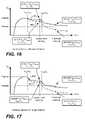
- FIG. 17is a graph representing a memory device that has a large sub-threshold swing factor.
- a memory cell having a threshold voltage just above the final verify levelis represented by solid line 460
- a memory cell having a threshold voltage just below the final verify levelis represented by dashed line 462 .
- the bit line voltage of each memory cellis pre-charged and the coarse verify level is applied to the selected word line. After applying the coarse verify level, the drain side select gate is turned on to connect the bit line to the NAND string of the cell. Because of the large S-factor for the device of FIG. 17 both memory cells cause a significant decrease in the voltage of their bit line even though the threshold voltage of both memory cells is above the coarse verify level V v1 .
- bit line voltageis sensed and compared with the reference potential V sense .
- the sense amplifiers for each celldetermine that both of these memory cells have a threshold voltage above the coarse verify level V v1 since the bit lines did not discharge to below V sense .
- the selected word lineis supplied with the final verify level V v2 .
- the memory cell having a threshold voltage just above the final verify level(solid line 460 ) is not as conductive as the memory cell having a threshold voltage just below the final verify level (dashed line 462 ).
- the large S-factor associated with the memorycauses the bit line voltage of the memory cell having a threshold voltage above the final verify level to discharge to below V sense .
- the memory cell having a threshold voltage below the final verify levelalso discharges its bit line to below V sense , as expected.
- the sense amplifier for the memory cell having a threshold voltage above the final verify leveldetermines that the cell's bit line has discharged to below V sense .
- the sense amplifierdetermines that the memory cell has a threshold voltage below the final verify level. This represents an error in the sense operation.
- the sense circuitrywill incorrectly determine that the memory cell is not yet programmed to its final target level and will cause the cell to undergo further programming.
- the memory cell represented by the dashed linealso has a sensed bit line voltage below V sense . The sense amplifier for this cell correctly determines that the threshold voltage of the cell is below the final verify level V v2 .
- FIG. 18is a graph of a coarse and fine verify and sensing approach in accordance with one embodiment of the present disclosure that can address bit line discharge resulting from large S-factor devices.
- the solid line 460again represents a memory cell having a threshold voltage just above the final verify level (e.g., V vA2 ).
- the dashed line 462represents a memory cell having a threshold voltage just below the final verify level.
- the bit line voltage of each memory cellis pre-charged to the predetermined level V clamp .
- the drain side select gateis then turned on to allow the bit line to discharge.
- the memory cell having a threshold voltage above the final verify levelwill again experience a somewhat significant decrease in bit line voltage because of the large S-factor. Similarly the memory cell having a threshold voltage below the final verify level also experiences a somewhat significant decrease in bit line voltage.
- the bit line voltage of each memory cellis sensed and compared with the reference potential.
- the sensed bit line voltageis compared with an intermediate reference potential V sense1 .
- the sense amplifiers for both memory cellswill determine that the bit line voltage is greater than the coarse verify level V sense1 .
- the sense amplifierscorrectly determine that the threshold voltage of each memory cell is greater than the coarse verify level V v1 .
- the selected word lineis supplied with the final verify level V v2 .
- the memory cell having a threshold voltage above the final verify levelwill conduct a significant amount of current because of the large S-factor of the device.
- the memory cell having a threshold voltage below the final verify levelis even more conductive, as expected, and discharges its bit line by a significant amount.
- the bit line voltage of each memory cellis sensed and compared with a reference potential.
- a different reference potentialis used.
- the sensed bit line voltageis compared with final reference potential V sense2 .
- V sense2is lower than V sense1 .
- the lower reference potentialcompensates for the bit line discharge that occurs under application of the coarse verify level. This compensation takes into account the large S-factor associated with the memory device that causes memory cells to discharge their bit line by a somewhat significant amount, even when the memory cell has a threshold voltage above the verify level.
- the memory cell having a threshold voltage just above the final verify levelhas its sensed bit line voltage compared with V sense2 .
- the sense amplifierwill determine that the bit line voltage is greater than the final reference potential V sense2 . Accordingly, the sense amplifier will correctly determine that the threshold voltage of this memory cell is greater than the final verify level V v2 .
- the sense amplifiercompares the sensed bit line voltage with the final reference potential V sense2 . The sense amplifier for this cell's bit line will determine that the bit line voltage is less than the final reference potential V sense2 . The sense amplifier will again correctly determine that the memory cell has a threshold voltage below the final verify level V v2 .
- the level of the reference potentialbetween coarse level sensing and fine level sensing when the bit line is not pre-charged again between each sense operation, a more accurate sensing of the state of the memory cells is achieved.
- the different in the reference potential levelsprovides a compensation for the amount of discharge during coarse level sensing.
- the final reference potential V sense2is less than the intermediate reference potential V sense1 by an amount that is approximately equal to the expected discharge of the bit line voltage for a memory cell having a threshold voltage above the coarse verify level V v1 when V v1 is applied to the memory cell's word line during coarse level sensing.
- a memory cell that is theoretically nonconductive under the applied verify levelwill have an associated bit line voltage discharge resulting from the large S-factor of the device.
- the difference between the intermediate and final V sense levelscan be set to approximately the difference between the bit line pre-charge level and the bit line voltage that results when the coarse verify level is applied to the word line. In this way, the final reference potential V sense2 compensates for the bit line discharge that results from a large S-factor device.
- V sense2may be set lower than V sense1 by an amount this is smaller than the expected discharge of a bit line for a memory cell when the coarse verify level is applied to the word line. A smaller offset of V sense2 relative to V sense1 may still accommodate the level of bit line discharge during coarse level sensing.
- the intermediate reference potential V sense1is approximately equal to the typical V sense level that would be used when devices have a normal or lower S-factor.
- the final reference potential V sense2is adjusted with reference to V sense1 by an amount that can compensate for a decrease in the bit line voltage during the coarse level sensing.
- a memory arrayundergoes testing during the manufacturing process.
- This testingcan include a characterization of the memory array's performance.
- the memory arraycan be measured to determine the amount that the bit lines will discharge when a coarse verify level is applied to the word line and the memory cell's threshold voltage is above this coarse verify level.
- the amount of discharge associated with multiple bit lines of the devicemay be averaged to arrive at an appropriate amount in one embodiment.
- the value of V sense2 relative to V sense1can be set to accommodate the measured decrease in bit line voltage under application of the coarse verify levels.
- the intermediate reference potential V sense1can be based on the characterization of the memory device.
- a selected subset of memory devicescan be tested and characterized, and the results of the characterization used to set the V sense1 and V sense2 levels for a larger set of devices including those of the subset.
- the manufacturing processcan set the levels of V sense1 and V sense2 for each memory device based on testing and characterization for that particular memory device. It is also possible to set the time period between turning on the select gate and performing the coarse level sensing to optimize accuracy in the coarse level sensing. Likewise, the time period between application of the final verify level to the selected word line and sensing at that level can be selected based on testing and characterization to further provide accurate sensing at both levels.
- the time before sensing during fine level sensingmay be established relative to the time the select gates are turned on during coarse level sensing or relative to the time the fine verify level is applied to the selected word line.
- Various techniquescan be used to set these values after the characterization. For instance, a set of anti-fuses, electrically programmable fuses, etc. may be provided within the memory device to store data relative to the operation of the device. These fuses may be set to store data indicating the values of V sense and/or the time periods for sensing.
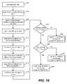
- FIG. 19is a flowchart describing a process for verifying programming of one or more memory cells.
- the process of FIG. 19is performed at step 362 of FIG. 11 after applying each program pulse at step 360 .
- the selected bit linesare pre-charged.
- pre-charging at step 402can include pre-charging the odd bit lines or the even bit lines.
- some architectureswill utilize an all bit line system such that step 502 will include charging each bit line of the selected block of memory cells.
- a read pass voltage V readis applied to each unselected word line at step 504 .
- Step 404ensures conduction of each unselected memory cell during the verification process so that only those memory cells connected to the selected word line will be verified.
- the coarse program verification voltageis applied to the selected word line.
- Step 506can include applying a coarse verify level such as V vA1 , V vB1 or V vC1 depending upon the number of states of the memory device being programmed.
- the drain side select gateis opened or turned on by applying a positive voltage on SGD. With the drain side select gate opened, the selected bit lines are connected to their NAND strings to permit discharge in accordance with the programmed state of the memory cell on that bit line that is connected to the selected word line. After a predetermined amount of time the voltages of the selected bit lines are sensed at step 510 .
- Step 510represents coarse level sensing for the memory device. After sensing the bit line voltages for each selected bit line, the bit line voltages are compared to an intermediate reference potential V sense1 at step 512 . At step 514 the selected word line is provided with the final verification voltage such as V vA2 , V vB2 or V vC2 depending upon the state or states that are being verified. At step 516 , the voltage of each selected bit line is sensed. Sensing at step 516 represents final or fine level sensing. At step 518 , the sensed bit line voltages are compared to the final reference potential V sense2 .
- the sense amplifier for each selected bit linewill determine if the sensed bit line voltage V BL is greater than the intermediate reference potential V sense1 using the results of the comparison at step 518 . If the sensed bit line voltage is less than the intermediate reference level, indicating that the memory cell's threshold voltage has not reached the coarse verification level, the memory cell is enabled for full programming at step 522 for the next iteration of the programming process. Step 522 can include applying a V enable voltage (e.g., ground) to the bit line of such a memory cell during the next programming pulse. If the bit line voltage was determined to be greater than V sense1 at step 520 , the process continues at step 524 .
- V enable voltagee.g., ground
- the sensed bit line voltage from the fine level sensing at step 516is compared to the final reference potential V sense2 . If the sense amplifier for a bit line determines that the bit line voltage is less than the final reference potential V sense2 , an intermediate voltage V S is applied to the bit line for the memory cell at step 526 for the next programming iteration. If the sense amplifier determines that the bit line voltage during fine level sensing is greater than the final reference potential V sense2 the sense amplifier causes V inhibit to be applied to the bit line at step 528 for the next program iteration.
- steps 502 through 528 of FIG. 19can be repeated for the number of verification operations that are needed to be performed in accordance with the number of potential states of the memory device.
- the verification at step 362can include three iterations of the method of FIG. 19 .
- the coarse and fine verification operationswill be performed once at the state A verify levels, once at the state B verify levels, and once at the state C verify levels. It is further noted that the results of sensing at a particular state's verify levels can be ignored for those selected bit lines that are being programmed to a different state than the one currently being verified.
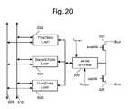
- FIG. 20depicts a portion of column control circuit 304 of FIG. 8 that includes a sense amplifier.
- Each pair of bit lines(e.g. BLe and BLo) is coupled to a sense amplifier 600 .
- the sense amplifieris connected to three data latches: first data latch 602 , second data latch 604 and third data latch 606 .
- Each of the three data latchesis capable of storing one bit of data.
- the sense amplifiersenses the potential level of the selected bit line during read or verify operations, stores the sensed data in a binary manner, and controls the bit line voltage during the program operation.
- the sense amplifieris selectively connected to the selected bit line by selecting one of signals of “evenBL” and “oddBL.”
- Data latches 602 , 604 and 606are coupled to I/O lines 608 to output read data and to store program data. I/O lines 608 are connected to data input/output buffer 312 of FIG. 8 .
- Data latches 602 , 604 and 606are also coupled to status line(s) 610 to receive and send status information.
- the data latchescan store the results of sensing in order to provide an enable voltage, inhibit voltage, or intermediate voltage to a bit line in accordance with the sensed state of the storage element relative to its target state, including coarse verify levels and final verify levels.
- two data latchescan be used to store the data to be programmed into a memory cell and the remaining data latch used to store an indication of whether a cell is currently in a fine programming phase or coarse programming phase.
- Sense amplifier 600can receive the different values of the reference potential to be used during the comparisons for the coarse level verify operation (V sense1 ) and the fine level verify operation (V sense2 ). The appropriate comparison level can be selected based on the data stored in the remaining data latch.
Landscapes
- Engineering & Computer Science (AREA)
- Microelectronics & Electronic Packaging (AREA)
- Computer Hardware Design (AREA)
- Read Only Memory (AREA)
Abstract
Description
Claims (22)
Priority Applications (7)
| Application Number | Priority Date | Filing Date | Title |
|---|---|---|---|
| US11/773,032US7508715B2 (en) | 2007-07-03 | 2007-07-03 | Coarse/fine program verification in non-volatile memory using different reference levels for improved sensing |
| JP2010515250AJP5198563B2 (en) | 2007-07-03 | 2008-07-02 | Versatile / high-precision program verification in non-volatile memory using different reference levels to improve sensing |
| EP08772349AEP2165338B1 (en) | 2007-07-03 | 2008-07-02 | Coarse/fine program verification in non-volatile memory using different reference levels for improved sensing |
| KR1020107002519AKR20100057784A (en) | 2007-07-03 | 2008-07-02 | Coarse/fine program verification in non-volatile memory using different reference levels for improved sensing |
| CN200880105358.3ACN101796591B (en) | 2007-07-03 | 2008-07-02 | Coarse/fine program verification in non-volatile memory using different reference levels for improved sensing |
| PCT/US2008/068988WO2009006513A1 (en) | 2007-07-03 | 2008-07-02 | Coarse/fine program verification in non-volatile memory using different reference levels for improved sensing |
| TW97125067ATWI389124B (en) | 2007-07-03 | 2008-07-03 | System and method for coarse/fine program verification in non-volatile memory using different reference levels for improved sensing |
Applications Claiming Priority (1)
| Application Number | Priority Date | Filing Date | Title |
|---|---|---|---|
| US11/773,032US7508715B2 (en) | 2007-07-03 | 2007-07-03 | Coarse/fine program verification in non-volatile memory using different reference levels for improved sensing |
Publications (2)
| Publication Number | Publication Date |
|---|---|
| US20090010067A1 US20090010067A1 (en) | 2009-01-08 |
| US7508715B2true US7508715B2 (en) | 2009-03-24 |
Family
ID=40221301
Family Applications (1)
| Application Number | Title | Priority Date | Filing Date |
|---|---|---|---|
| US11/773,032ActiveUS7508715B2 (en) | 2007-07-03 | 2007-07-03 | Coarse/fine program verification in non-volatile memory using different reference levels for improved sensing |
Country Status (1)
| Country | Link |
|---|---|
| US (1) | US7508715B2 (en) |
Cited By (21)
| Publication number | Priority date | Publication date | Assignee | Title |
|---|---|---|---|---|
| US20090073763A1 (en)* | 2007-09-14 | 2009-03-19 | Kabushiki Kaisha Toshiba | Method for controlling a non-volatile semiconductor memory device |
| US20090207657A1 (en)* | 2008-02-15 | 2009-08-20 | Satoru Tamada | Multi level inhibit scheme |
| US20090219761A1 (en)* | 2008-02-29 | 2009-09-03 | Micron Technology, Inc. | Charge loss compensation during programming of a memory device |
| US20090310419A1 (en)* | 2008-06-12 | 2009-12-17 | Raul-Adrian Cernea | Nonvolatile Memory with Index Programming and Reduced Verify |
| US20090310421A1 (en)* | 2008-06-12 | 2009-12-17 | Raul-Adrian Cernea | Nonvolatile Memory with Correlated Multiple Pass Programming |
| US20090310420A1 (en)* | 2008-06-12 | 2009-12-17 | Raul-Adrian Cernea | Method for Correlated Multiple Pass Programming in Nonvolatile Memory |
| US20090310418A1 (en)* | 2008-06-12 | 2009-12-17 | Raul-Adrian Cernea | Method for Index Programming and Reduced Verify in Nonvolatile Memory |
| US20100046297A1 (en)* | 2008-08-25 | 2010-02-25 | Raul-Adrian Cernea | Non-volatile memory and method for ramp-down programming |
| US20100097857A1 (en)* | 2007-04-10 | 2010-04-22 | Raul-Adrian Cernea | Predictive Programming in Non-Volatile Memory |
| US20100208524A1 (en)* | 2009-02-19 | 2010-08-19 | Micron Technology, Inc. | Soft landing for desired program threshold voltage |
| US20130208545A1 (en)* | 2012-02-09 | 2013-08-15 | SK Hynix Inc. | Semiconductor memory apparatus, program method thereof, and data processing system using the same |
| US8514624B2 (en) | 2011-06-21 | 2013-08-20 | Micron Technology, Inc. | In-field block retiring |
| US9129709B2 (en) | 2011-10-05 | 2015-09-08 | Samsung Electronics Co., Ltd. | Memory system comprising non-volatile memory device and related method of operation |
| US9437302B2 (en) | 2014-02-06 | 2016-09-06 | Sandisk Technologies Llc | State-dependent lockout in non-volatile memory |
| US9548130B2 (en) | 2015-04-08 | 2017-01-17 | Sandisk Technologies Llc | Non-volatile memory with prior state sensing |
| US9570179B2 (en) | 2015-04-22 | 2017-02-14 | Sandisk Technologies Llc | Non-volatile memory with two phased programming |
| US9875805B2 (en) | 2015-01-23 | 2018-01-23 | Sandisk Technologies Llc | Double lockout in non-volatile memory |
| US11049578B1 (en) | 2020-02-19 | 2021-06-29 | Sandisk Technologies Llc | Non-volatile memory with program verify skip |
| US11532370B1 (en) | 2021-05-25 | 2022-12-20 | Sandisk Technologies Llc | Non-volatile memory with fast multi-level program verify |
| US20240126642A1 (en)* | 2022-10-17 | 2024-04-18 | SK Hynix Inc. | Storage device |
| US12094546B2 (en) | 2022-01-31 | 2024-09-17 | Sandisk Technologies Llc | Non-volatile memory with zone based program speed adjustment |
Families Citing this family (21)
| Publication number | Priority date | Publication date | Assignee | Title |
|---|---|---|---|---|
| US8200887B2 (en) | 2007-03-29 | 2012-06-12 | Violin Memory, Inc. | Memory management system and method |
| US9384818B2 (en) | 2005-04-21 | 2016-07-05 | Violin Memory | Memory power management |
| US9286198B2 (en) | 2005-04-21 | 2016-03-15 | Violin Memory | Method and system for storage of data in non-volatile media |
| US8452929B2 (en)* | 2005-04-21 | 2013-05-28 | Violin Memory Inc. | Method and system for storage of data in non-volatile media |
| US8028186B2 (en) | 2006-10-23 | 2011-09-27 | Violin Memory, Inc. | Skew management in an interconnection system |
| US9632870B2 (en) | 2007-03-29 | 2017-04-25 | Violin Memory, Inc. | Memory system with multiple striping of raid groups and method for performing the same |
| US11010076B2 (en) | 2007-03-29 | 2021-05-18 | Violin Systems Llc | Memory system with multiple striping of raid groups and method for performing the same |
| CN102576330B (en) | 2009-06-12 | 2015-01-28 | 提琴存储器公司 | Storage system with persistent garbage collection mechanism |
| US8081514B2 (en)* | 2009-08-25 | 2011-12-20 | Sandisk Technologies Inc. | Partial speed and full speed programming for non-volatile memory using floating bit lines |
| US8218381B2 (en)* | 2009-11-24 | 2012-07-10 | Sandisk Technologies Inc. | Programming memory with sensing-based bit line compensation to reduce channel-to-floating gate coupling |
| KR20110131648A (en) | 2010-05-31 | 2011-12-07 | 삼성전자주식회사 | Non-volatile memory device, memory system and memory card including it and program method thereof |
| KR101658118B1 (en)* | 2010-06-10 | 2016-09-20 | 삼성전자 주식회사 | Semiconductor memory device, and reading and verifying method of the same |
| US8274838B2 (en)* | 2010-07-19 | 2012-09-25 | Sandisk Technologies Inc. | Programming non-volatile memory with bit line voltage step up |
| US9136006B2 (en)* | 2013-03-11 | 2015-09-15 | Macronix International Co., Ltd. | Method and device for reducing coupling noise during read operation |
| KR20160108770A (en) | 2015-03-06 | 2016-09-20 | 에스케이하이닉스 주식회사 | Semiconductor memory device and operating method thereof |
| KR20160129430A (en)* | 2015-04-30 | 2016-11-09 | 에스케이하이닉스 주식회사 | Semiconductor memory device and programming method thereof |
| US9633719B2 (en)* | 2015-05-29 | 2017-04-25 | Micron Technology, Inc. | Programming memory cells to be programmed to different levels to an intermediate level from a lowest level |
| JP2018113084A (en)* | 2017-01-06 | 2018-07-19 | 東芝メモリ株式会社 | Semiconductor memory device |
| US9842657B1 (en)* | 2017-05-18 | 2017-12-12 | Sandisk Technologies Llc | Multi-state program using controlled weak boosting for non-volatile memory |
| JP6887044B1 (en)* | 2020-05-22 | 2021-06-16 | ウィンボンド エレクトロニクス コーポレーション | Semiconductor storage device and readout method |
| US12112800B2 (en)* | 2022-05-26 | 2024-10-08 | Sandisk Technologies Llc | High speed multi-level cell (MLC) programming in non-volatile memory structures |
Citations (87)
| Publication number | Priority date | Publication date | Assignee | Title |
|---|---|---|---|---|
| US4357685A (en) | 1979-09-28 | 1982-11-02 | Sgs-Ates Componenti Elettronici S.P.A. | Method of programming an electrically alterable nonvolatile memory |
| US4627027A (en) | 1982-09-01 | 1986-12-02 | Sanyo Electric Co., Ltd. | Analog storing and reproducing apparatus utilizing non-volatile memory elements |
| US5053990A (en) | 1988-02-17 | 1991-10-01 | Intel Corporation | Program/erase selection for flash memory |
| US5122985A (en)* | 1990-04-16 | 1992-06-16 | Giovani Santin | Circuit and method for erasing eeprom memory arrays to prevent over-erased cells |
| US5220531A (en) | 1991-01-02 | 1993-06-15 | Information Storage Devices, Inc. | Source follower storage cell and improved method and apparatus for iterative write for integrated circuit analog signal recording and playback |
| US5313421A (en) | 1992-01-14 | 1994-05-17 | Sundisk Corporation | EEPROM with split gate source side injection |
| US5386422A (en) | 1991-03-12 | 1995-01-31 | Kabushiki Kaisha Toshiba | Electrically erasable and programmable non-volatile memory system with write-verify controller using two reference levels |
| US5412601A (en) | 1992-08-31 | 1995-05-02 | Nippon Steel Corporation | Non-volatile semiconductor memory device capable of storing multi-value data in each memory cell |
| US5428568A (en)* | 1991-10-30 | 1995-06-27 | Mitsubishi Denki Kabushiki Kaisha | Electrically erasable and programmable non-volatile memory device and a method of operating the same |
| US5521865A (en) | 1994-03-15 | 1996-05-28 | Kabushiki Kaisha Toshiba | Non-volatile semiconductor memory device for storing multi-value data |
| US5528546A (en)* | 1993-08-31 | 1996-06-18 | Macronix International Company, Ltd. | Erase and program verification circuit for non-volatile memory |
| US5570315A (en) | 1993-09-21 | 1996-10-29 | Kabushiki Kaisha Toshiba | Multi-state EEPROM having write-verify control circuit |
| US5596532A (en) | 1995-10-18 | 1997-01-21 | Sandisk Corporation | Flash EEPROM self-adaptive voltage generation circuit operative within a continuous voltage source range |
| US5623442A (en) | 1993-07-13 | 1997-04-22 | Nkk Corporation | Memory cells and memory devices with a storage capacitor of parasitic capacitance and information storing method using the same |
| US5712815A (en) | 1996-04-22 | 1998-01-27 | Advanced Micro Devices, Inc. | Multiple bits per-cell flash EEPROM capable of concurrently programming and verifying memory cells and reference cells |
| US5712180A (en) | 1992-01-14 | 1998-01-27 | Sundisk Corporation | EEPROM with split gate source side injection |
| US5729494A (en) | 1993-05-11 | 1998-03-17 | Nkk Corporation | Non-volatile memory with floating gate type cell transistors and method for adjusting threshold valves of these transistors |
| US5761222A (en) | 1994-09-30 | 1998-06-02 | Sgs-Thomson Microelectronics, S.R.L. | Memory device having error detection and correction function, and methods for reading, writing and erasing the memory device |
| US5768191A (en)* | 1995-12-07 | 1998-06-16 | Samsung Electronics Co., Ltd. | Methods of programming multi-state integrated circuit memory devices |
| WO1998028745A1 (en) | 1996-12-20 | 1998-07-02 | Intel Corporation | Nonvolatile writeable memory with fast programming capability |
| US5808938A (en) | 1996-04-09 | 1998-09-15 | Information Storage Devices, Inc. | Method and apparatus for reading analog values stored in floating gate nand structures |
| EP0877386A1 (en) | 1997-05-09 | 1998-11-11 | STMicroelectronics S.r.l. | Method and device for analog programming of non-volatile memory cells, in particular flash memory cells |
| US5870344A (en) | 1996-03-14 | 1999-02-09 | Fujitsu Limited | Semiconductor memory device |
| US5870334A (en) | 1994-09-17 | 1999-02-09 | Kabushiki Kaisha Toshiba | Nonvolatile semiconductor memory device |
| US5877984A (en) | 1997-09-05 | 1999-03-02 | Information Storage Devices, Inc. | Method and apparatus for adjustment and control of an iterative method of recording analog signals with on chip selection of a voltage ramp amplitude |
| US5880993A (en) | 1996-09-30 | 1999-03-09 | Sgs-Thomson Microelectronics, S.R.L. | Method and circuit for checking multilevel programming of floating-gate nonvolatile memory cells particularly flash cells |
| US5912836A (en) | 1997-12-01 | 1999-06-15 | Amic Technology, Inc. | Circuit for detecting both charge gain and charge loss properties in a non-volatile memory array |
| US5926409A (en) | 1997-09-05 | 1999-07-20 | Information Storage Devices, Inc. | Method and apparatus for an adaptive ramp amplitude controller in nonvolatile memory application |
| US5943260A (en) | 1997-02-21 | 1999-08-24 | Nec Corporation | Method for high-speed programming of a nonvolatile semiconductor memory device |
| US5969986A (en) | 1998-06-23 | 1999-10-19 | Invox Technology | High-bandwidth read and write architectures for non-volatile memories |
| US5969990A (en) | 1997-01-31 | 1999-10-19 | Sony Corporation | Nonvolatile memory array with NAND string memory cell groups selectively connected to sub bit lines |
| US5991202A (en) | 1998-09-24 | 1999-11-23 | Advanced Micro Devices, Inc. | Method for reducing program disturb during self-boosting in a NAND flash memory |
| US6091637A (en)* | 1997-09-25 | 2000-07-18 | Sharp Kabushiki Kaisha | Method for writing data into non-volatile semiconductor memory cell |
| US6125052A (en) | 1997-09-18 | 2000-09-26 | Kabushiki Kaisha Toshiba | Semiconductor memory device |
| US6128224A (en) | 1998-07-29 | 2000-10-03 | Motorola, Inc. | Method and apparatus for writing an erasable non-volatile memory |
| US6151248A (en) | 1999-06-30 | 2000-11-21 | Sandisk Corporation | Dual floating gate EEPROM cell array with steering gates shared by adjacent cells |
| US6222762B1 (en) | 1992-01-14 | 2001-04-24 | Sandisk Corporation | Multi-state memory |
| US6243290B1 (en) | 1999-08-31 | 2001-06-05 | Hitachi, Ltd. | Nonvolatile semiconductor memory device |
| US6266270B1 (en) | 1998-07-23 | 2001-07-24 | Sony Corporation | Non-volatile semiconductor memory and programming method of the same |
| US6278634B1 (en) | 1999-06-29 | 2001-08-21 | Hyundai Electronics Industries Co., Ltd. | Reference memory cell initialization circuit and method |
| US6278632B1 (en) | 1996-10-24 | 2001-08-21 | Micron Technology, Inc. | Method and circuitry for performing analog over-program and under-program detection for a multistate memory cell |
| US6292394B1 (en) | 2000-06-29 | 2001-09-18 | Saifun Semiconductors Ltd. | Method for programming of a semiconductor memory cell |
| US6301151B1 (en) | 2000-08-09 | 2001-10-09 | Information Storage Devices, Inc. | Adaptive programming method and apparatus for flash memory analog storage |
| US6301161B1 (en)* | 2000-04-25 | 2001-10-09 | Winbond Electronics Corporation | Programming flash memory analog storage using coarse-and-fine sequence |
| US20010040824A1 (en) | 1991-02-08 | 2001-11-15 | Banks Gerald J. | Electrically alterable non-volatile memory with n-bits per cell |
| US6343033B1 (en) | 2000-02-25 | 2002-01-29 | Advanced Micro Devices, Inc. | Variable pulse width memory programming |
| US6363010B2 (en) | 1996-03-18 | 2002-03-26 | Kabushiki Kaisha Toshiba | Nonvolatile semiconductor memory device |
| US6392931B1 (en) | 1998-11-27 | 2002-05-21 | Stmicroelectronics S.R.L. | Method for high precision programming nonvolatile memory cells, with optimized programming speed |
| US6424566B1 (en) | 2001-02-08 | 2002-07-23 | Advanced Micro Devices, Inc. | Program reconnaissance to eliminate variations in vt distributions of multi-level cell flash memory designs |
| EP1225596A2 (en) | 2000-12-07 | 2002-07-24 | Saifun Semiconductors Ltd. | Programming and erasing methods for a reference cell of an NROM array |
| EP1249842A1 (en) | 2001-04-10 | 2002-10-16 | STMicroelectronics S.r.l. | Method for programming nonvolatile memory cells with program and verify algorithm using a staircase voltage with varying step amplitude |
| US6504761B2 (en) | 2001-02-13 | 2003-01-07 | Mitsubishi Denki Kabushiki Kaisha | Non-volatile semiconductor memory device improved sense amplification configuration |
| US6519184B2 (en) | 2001-04-19 | 2003-02-11 | Hitachi, Ltd. | Non-volatile memory device with plurality of threshold voltage distributions |
| US6522580B2 (en) | 2001-06-27 | 2003-02-18 | Sandisk Corporation | Operating techniques for reducing effects of coupling between storage elements of a non-volatile memory operated in multiple data states |
| US6525964B2 (en) | 1997-04-07 | 2003-02-25 | Kabushiki Kaisha Toshiba | Semiconductor memory device |
| US6529412B1 (en) | 2002-01-16 | 2003-03-04 | Advanced Micro Devices, Inc. | Source side sensing scheme for virtual ground read of flash eprom array with adjacent bit precharge |
| US6532172B2 (en) | 2001-05-31 | 2003-03-11 | Sandisk Corporation | Steering gate and bit line segmentation in non-volatile memories |
| US6590811B1 (en) | 2001-02-28 | 2003-07-08 | Advanced Micro Devices, Inc. | Higher program VT and faster programming rates based on improved erase methods |
| EP1341185A1 (en) | 2002-02-27 | 2003-09-03 | SanDisk Corporation | Operating techniques for reducing the program and read disturbs of a non-volatile memory |
| US6643188B2 (en) | 2001-12-27 | 2003-11-04 | Kabushiki Kaisha Toshiba | Non-volatile semiconductor memory device adapted to store a multi-valued data in a single memory cell |
| US6674668B2 (en) | 1999-12-28 | 2004-01-06 | Kabushiki Kaisha Toshiba | Read circuit on nonvolatile semiconductor memory |
| US6735114B1 (en) | 2003-02-04 | 2004-05-11 | Advanced Micro Devices, Inc. | Method of improving dynamic reference tracking for flash memory unit |
| US6738289B2 (en) | 2001-02-26 | 2004-05-18 | Sandisk Corporation | Non-volatile memory with improved programming and method therefor |
| US6747892B2 (en) | 2000-11-21 | 2004-06-08 | Sandisk Corporation | Sense amplifier for multilevel non-volatile integrated memory devices |
| US20040109352A1 (en) | 2002-12-05 | 2004-06-10 | Kyeong-Han Lee | Flash memory device having uniform threshold voltage distribution and method for verifying same |
| US20040141377A1 (en) | 2002-11-29 | 2004-07-22 | Fumitaka Arai | Nonvolatile semiconductor memory device and data program method thereof |
| US6785164B2 (en) | 2002-01-18 | 2004-08-31 | Sandisk Corporation | Reducing the effects of noise in non-volatile memories through multiple reads |
| US6809962B2 (en) | 2002-03-14 | 2004-10-26 | Intel Corporation | Storing data in-non-volatile memory devices |
| US6829167B2 (en) | 2002-12-12 | 2004-12-07 | Sandisk Corporation | Error recovery for nonvolatile memory |
| US6856551B2 (en) | 2003-02-06 | 2005-02-15 | Sandisk Corporation | System and method for programming cells in non-volatile integrated memory devices |
| US6859397B2 (en) | 2003-03-05 | 2005-02-22 | Sandisk Corporation | Source side self boosting technique for non-volatile memory |
| US20050057967A1 (en) | 2003-09-17 | 2005-03-17 | Shahzad Khalid | Non-volatile memory and method with bit line compensation dependent on neighboring operating modes |
| US20050057968A1 (en) | 2003-09-17 | 2005-03-17 | Sandisk Corporation | Methods for identifying non-volatile memory elements with poor subthreshold slope or weak transconductance |
| US20050057965A1 (en) | 2003-09-17 | 2005-03-17 | Raul-Adrian Cernea | Non-volatile memory and method with bit line coupled compensation |
| US20050083735A1 (en) | 2003-10-20 | 2005-04-21 | Jian Chen | Behavior based programming of non-volatile memory |
| US6888758B1 (en) | 2004-01-21 | 2005-05-03 | Sandisk Corporation | Programming non-volatile memory |
| US6894929B2 (en) | 2003-05-12 | 2005-05-17 | Sharp Kabushiki Kaisha | Method of programming semiconductor memory device having memory cells and method of erasing the same |
| US6924663B2 (en) | 2001-12-28 | 2005-08-02 | Fujitsu Limited | Programmable logic device with ferroelectric configuration memories |
| US6958934B2 (en) | 2002-01-17 | 2005-10-25 | Macronix International Co., Ltd. | Method of programming and erasing multi-level flash memory |
| US7002843B2 (en) | 2004-01-27 | 2006-02-21 | Sandisk Corporation | Variable current sinking for coarse/fine programming of non-volatile memory |
| US7020026B2 (en) | 2004-05-05 | 2006-03-28 | Sandisk Corporation | Bitline governed approach for program control of non-volatile memory |
| US7023733B2 (en) | 2004-05-05 | 2006-04-04 | Sandisk Corporation | Boosting to control programming of non-volatile memory |
| US7068539B2 (en) | 2004-01-27 | 2006-06-27 | Sandisk Corporation | Charge packet metering for coarse/fine programming of non-volatile memory |
| US7092290B2 (en) | 2004-11-16 | 2006-08-15 | Sandisk Corporation | High speed programming system with reduced over programming |
| WO2006107651A1 (en) | 2005-04-01 | 2006-10-12 | Sandisk Corporation | Multi-state memory having data recovery after program fail |
| US7139198B2 (en)* | 2004-01-27 | 2006-11-21 | Sandisk Corporation | Efficient verification for coarse/fine programming of non-volatile memory |
| US7173859B2 (en) | 2004-11-16 | 2007-02-06 | Sandisk Corporation | Faster programming of higher level states in multi-level cell flash memory |
- 2007
- 2007-07-03USUS11/773,032patent/US7508715B2/enactiveActive
Patent Citations (98)
| Publication number | Priority date | Publication date | Assignee | Title |
|---|---|---|---|---|
| US4357685A (en) | 1979-09-28 | 1982-11-02 | Sgs-Ates Componenti Elettronici S.P.A. | Method of programming an electrically alterable nonvolatile memory |
| US4627027A (en) | 1982-09-01 | 1986-12-02 | Sanyo Electric Co., Ltd. | Analog storing and reproducing apparatus utilizing non-volatile memory elements |
| US5053990A (en) | 1988-02-17 | 1991-10-01 | Intel Corporation | Program/erase selection for flash memory |
| US5122985A (en)* | 1990-04-16 | 1992-06-16 | Giovani Santin | Circuit and method for erasing eeprom memory arrays to prevent over-erased cells |
| US5220531A (en) | 1991-01-02 | 1993-06-15 | Information Storage Devices, Inc. | Source follower storage cell and improved method and apparatus for iterative write for integrated circuit analog signal recording and playback |
| US20010040824A1 (en) | 1991-02-08 | 2001-11-15 | Banks Gerald J. | Electrically alterable non-volatile memory with n-bits per cell |
| US5386422A (en) | 1991-03-12 | 1995-01-31 | Kabushiki Kaisha Toshiba | Electrically erasable and programmable non-volatile memory system with write-verify controller using two reference levels |
| US5469444A (en)* | 1991-03-12 | 1995-11-21 | Kabushiki Kaisha Toshiba | Electrically erasable and programmable non-volatile memory system with write-verify controller using two reference levels |
| US5428568A (en)* | 1991-10-30 | 1995-06-27 | Mitsubishi Denki Kabushiki Kaisha | Electrically erasable and programmable non-volatile memory device and a method of operating the same |
| US5313421A (en) | 1992-01-14 | 1994-05-17 | Sundisk Corporation | EEPROM with split gate source side injection |
| US6222762B1 (en) | 1992-01-14 | 2001-04-24 | Sandisk Corporation | Multi-state memory |
| US6317364B1 (en) | 1992-01-14 | 2001-11-13 | Sandisk Corporation | Multi-state memory |
| US5712180A (en) | 1992-01-14 | 1998-01-27 | Sundisk Corporation | EEPROM with split gate source side injection |
| US5412601A (en) | 1992-08-31 | 1995-05-02 | Nippon Steel Corporation | Non-volatile semiconductor memory device capable of storing multi-value data in each memory cell |
| US5729494A (en) | 1993-05-11 | 1998-03-17 | Nkk Corporation | Non-volatile memory with floating gate type cell transistors and method for adjusting threshold valves of these transistors |
| US5623442A (en) | 1993-07-13 | 1997-04-22 | Nkk Corporation | Memory cells and memory devices with a storage capacitor of parasitic capacitance and information storing method using the same |
| US5528546A (en)* | 1993-08-31 | 1996-06-18 | Macronix International Company, Ltd. | Erase and program verification circuit for non-volatile memory |
| US5652719A (en) | 1993-09-21 | 1997-07-29 | Kabushiki Kaisha Toshiba | Nonvolatile semiconductor memory device |
| US5570315A (en) | 1993-09-21 | 1996-10-29 | Kabushiki Kaisha Toshiba | Multi-state EEPROM having write-verify control circuit |
| US5521865A (en) | 1994-03-15 | 1996-05-28 | Kabushiki Kaisha Toshiba | Non-volatile semiconductor memory device for storing multi-value data |
| US5870334A (en) | 1994-09-17 | 1999-02-09 | Kabushiki Kaisha Toshiba | Nonvolatile semiconductor memory device |
| US5949714A (en) | 1994-09-17 | 1999-09-07 | Kabushiki Kaisha Toshiba | Nonvolatile semiconductor memory device |
| US5761222A (en) | 1994-09-30 | 1998-06-02 | Sgs-Thomson Microelectronics, S.R.L. | Memory device having error detection and correction function, and methods for reading, writing and erasing the memory device |
| US5596532A (en) | 1995-10-18 | 1997-01-21 | Sandisk Corporation | Flash EEPROM self-adaptive voltage generation circuit operative within a continuous voltage source range |
| US5768191A (en)* | 1995-12-07 | 1998-06-16 | Samsung Electronics Co., Ltd. | Methods of programming multi-state integrated circuit memory devices |
| US5870344A (en) | 1996-03-14 | 1999-02-09 | Fujitsu Limited | Semiconductor memory device |
| US6363010B2 (en) | 1996-03-18 | 2002-03-26 | Kabushiki Kaisha Toshiba | Nonvolatile semiconductor memory device |
| US5909393A (en) | 1996-04-09 | 1999-06-01 | Information Storage Devices, Inc. | Method and apparatus for reading analog values stored in floating gate NAND structures |
| US5808938A (en) | 1996-04-09 | 1998-09-15 | Information Storage Devices, Inc. | Method and apparatus for reading analog values stored in floating gate nand structures |
| US5712815A (en) | 1996-04-22 | 1998-01-27 | Advanced Micro Devices, Inc. | Multiple bits per-cell flash EEPROM capable of concurrently programming and verifying memory cells and reference cells |
| US5880993A (en) | 1996-09-30 | 1999-03-09 | Sgs-Thomson Microelectronics, S.R.L. | Method and circuit for checking multilevel programming of floating-gate nonvolatile memory cells particularly flash cells |
| US6278632B1 (en) | 1996-10-24 | 2001-08-21 | Micron Technology, Inc. | Method and circuitry for performing analog over-program and under-program detection for a multistate memory cell |
| WO1998028745A1 (en) | 1996-12-20 | 1998-07-02 | Intel Corporation | Nonvolatile writeable memory with fast programming capability |
| US5969990A (en) | 1997-01-31 | 1999-10-19 | Sony Corporation | Nonvolatile memory array with NAND string memory cell groups selectively connected to sub bit lines |
| US5943260A (en) | 1997-02-21 | 1999-08-24 | Nec Corporation | Method for high-speed programming of a nonvolatile semiconductor memory device |
| US6525964B2 (en) | 1997-04-07 | 2003-02-25 | Kabushiki Kaisha Toshiba | Semiconductor memory device |
| EP0877386A1 (en) | 1997-05-09 | 1998-11-11 | STMicroelectronics S.r.l. | Method and device for analog programming of non-volatile memory cells, in particular flash memory cells |
| US5877984A (en) | 1997-09-05 | 1999-03-02 | Information Storage Devices, Inc. | Method and apparatus for adjustment and control of an iterative method of recording analog signals with on chip selection of a voltage ramp amplitude |
| US5926409A (en) | 1997-09-05 | 1999-07-20 | Information Storage Devices, Inc. | Method and apparatus for an adaptive ramp amplitude controller in nonvolatile memory application |
| US6125052A (en) | 1997-09-18 | 2000-09-26 | Kabushiki Kaisha Toshiba | Semiconductor memory device |
| US6091637A (en)* | 1997-09-25 | 2000-07-18 | Sharp Kabushiki Kaisha | Method for writing data into non-volatile semiconductor memory cell |
| US5912836A (en) | 1997-12-01 | 1999-06-15 | Amic Technology, Inc. | Circuit for detecting both charge gain and charge loss properties in a non-volatile memory array |
| US5969986A (en) | 1998-06-23 | 1999-10-19 | Invox Technology | High-bandwidth read and write architectures for non-volatile memories |
| US6266270B1 (en) | 1998-07-23 | 2001-07-24 | Sony Corporation | Non-volatile semiconductor memory and programming method of the same |
| US6128224A (en) | 1998-07-29 | 2000-10-03 | Motorola, Inc. | Method and apparatus for writing an erasable non-volatile memory |
| US5991202A (en) | 1998-09-24 | 1999-11-23 | Advanced Micro Devices, Inc. | Method for reducing program disturb during self-boosting in a NAND flash memory |
| US6392931B1 (en) | 1998-11-27 | 2002-05-21 | Stmicroelectronics S.R.L. | Method for high precision programming nonvolatile memory cells, with optimized programming speed |
| US6278634B1 (en) | 1999-06-29 | 2001-08-21 | Hyundai Electronics Industries Co., Ltd. | Reference memory cell initialization circuit and method |
| US6151248A (en) | 1999-06-30 | 2000-11-21 | Sandisk Corporation | Dual floating gate EEPROM cell array with steering gates shared by adjacent cells |
| US6344993B1 (en) | 1999-06-30 | 2002-02-05 | Sandisk Corporation | Dual floating gate EEPROM cell array with steering gates shared by adjacent cells |
| US6243290B1 (en) | 1999-08-31 | 2001-06-05 | Hitachi, Ltd. | Nonvolatile semiconductor memory device |
| US6674668B2 (en) | 1999-12-28 | 2004-01-06 | Kabushiki Kaisha Toshiba | Read circuit on nonvolatile semiconductor memory |
| US20040057326A1 (en) | 1999-12-28 | 2004-03-25 | Kabushiki Kaisha Toshiba | Read circuit of nonvolatile semiconductor memory |
| US6343033B1 (en) | 2000-02-25 | 2002-01-29 | Advanced Micro Devices, Inc. | Variable pulse width memory programming |
| US6301161B1 (en)* | 2000-04-25 | 2001-10-09 | Winbond Electronics Corporation | Programming flash memory analog storage using coarse-and-fine sequence |
| US6292394B1 (en) | 2000-06-29 | 2001-09-18 | Saifun Semiconductors Ltd. | Method for programming of a semiconductor memory cell |
| US6301151B1 (en) | 2000-08-09 | 2001-10-09 | Information Storage Devices, Inc. | Adaptive programming method and apparatus for flash memory analog storage |
| US6747892B2 (en) | 2000-11-21 | 2004-06-08 | Sandisk Corporation | Sense amplifier for multilevel non-volatile integrated memory devices |
| EP1225596A2 (en) | 2000-12-07 | 2002-07-24 | Saifun Semiconductors Ltd. | Programming and erasing methods for a reference cell of an NROM array |
| US6424566B1 (en) | 2001-02-08 | 2002-07-23 | Advanced Micro Devices, Inc. | Program reconnaissance to eliminate variations in vt distributions of multi-level cell flash memory designs |
| US6504761B2 (en) | 2001-02-13 | 2003-01-07 | Mitsubishi Denki Kabushiki Kaisha | Non-volatile semiconductor memory device improved sense amplification configuration |
| US6738289B2 (en) | 2001-02-26 | 2004-05-18 | Sandisk Corporation | Non-volatile memory with improved programming and method therefor |
| US6590811B1 (en) | 2001-02-28 | 2003-07-08 | Advanced Micro Devices, Inc. | Higher program VT and faster programming rates based on improved erase methods |
| US6788579B2 (en) | 2001-04-10 | 2004-09-07 | Stmicroelectronics S.R.L. | Method for programming nonvolatile memory cells with program and verify algorithm using a staircase voltage with varying step amplitude |
| EP1249842A1 (en) | 2001-04-10 | 2002-10-16 | STMicroelectronics S.r.l. | Method for programming nonvolatile memory cells with program and verify algorithm using a staircase voltage with varying step amplitude |
| US6519184B2 (en) | 2001-04-19 | 2003-02-11 | Hitachi, Ltd. | Non-volatile memory device with plurality of threshold voltage distributions |
| US6532172B2 (en) | 2001-05-31 | 2003-03-11 | Sandisk Corporation | Steering gate and bit line segmentation in non-volatile memories |
| US6522580B2 (en) | 2001-06-27 | 2003-02-18 | Sandisk Corporation | Operating techniques for reducing effects of coupling between storage elements of a non-volatile memory operated in multiple data states |
| US6643188B2 (en) | 2001-12-27 | 2003-11-04 | Kabushiki Kaisha Toshiba | Non-volatile semiconductor memory device adapted to store a multi-valued data in a single memory cell |
| US6924663B2 (en) | 2001-12-28 | 2005-08-02 | Fujitsu Limited | Programmable logic device with ferroelectric configuration memories |
| US6529412B1 (en) | 2002-01-16 | 2003-03-04 | Advanced Micro Devices, Inc. | Source side sensing scheme for virtual ground read of flash eprom array with adjacent bit precharge |
| US6958934B2 (en) | 2002-01-17 | 2005-10-25 | Macronix International Co., Ltd. | Method of programming and erasing multi-level flash memory |
| US6785164B2 (en) | 2002-01-18 | 2004-08-31 | Sandisk Corporation | Reducing the effects of noise in non-volatile memories through multiple reads |
| US6952365B2 (en) | 2002-01-18 | 2005-10-04 | Sandisk Corporation | Reducing the effects of noise in non-volatile memories through multiple reads |
| EP1341185A1 (en) | 2002-02-27 | 2003-09-03 | SanDisk Corporation | Operating techniques for reducing the program and read disturbs of a non-volatile memory |
| US6809962B2 (en) | 2002-03-14 | 2004-10-26 | Intel Corporation | Storing data in-non-volatile memory devices |
| US20040141377A1 (en) | 2002-11-29 | 2004-07-22 | Fumitaka Arai | Nonvolatile semiconductor memory device and data program method thereof |
| US20040109352A1 (en) | 2002-12-05 | 2004-06-10 | Kyeong-Han Lee | Flash memory device having uniform threshold voltage distribution and method for verifying same |
| US6853585B2 (en)* | 2002-12-05 | 2005-02-08 | Samsung Electronics Co., Ltd. | Flash memory device having uniform threshold voltage distribution and method for verifying same |
| US6829167B2 (en) | 2002-12-12 | 2004-12-07 | Sandisk Corporation | Error recovery for nonvolatile memory |
| US6735114B1 (en) | 2003-02-04 | 2004-05-11 | Advanced Micro Devices, Inc. | Method of improving dynamic reference tracking for flash memory unit |
| US6856551B2 (en) | 2003-02-06 | 2005-02-15 | Sandisk Corporation | System and method for programming cells in non-volatile integrated memory devices |
| US6859397B2 (en) | 2003-03-05 | 2005-02-22 | Sandisk Corporation | Source side self boosting technique for non-volatile memory |
| US6894929B2 (en) | 2003-05-12 | 2005-05-17 | Sharp Kabushiki Kaisha | Method of programming semiconductor memory device having memory cells and method of erasing the same |
| US20050057967A1 (en) | 2003-09-17 | 2005-03-17 | Shahzad Khalid | Non-volatile memory and method with bit line compensation dependent on neighboring operating modes |
| US20050057968A1 (en) | 2003-09-17 | 2005-03-17 | Sandisk Corporation | Methods for identifying non-volatile memory elements with poor subthreshold slope or weak transconductance |
| US20050057965A1 (en) | 2003-09-17 | 2005-03-17 | Raul-Adrian Cernea | Non-volatile memory and method with bit line coupled compensation |
| US20050083735A1 (en) | 2003-10-20 | 2005-04-21 | Jian Chen | Behavior based programming of non-volatile memory |
| US6888758B1 (en) | 2004-01-21 | 2005-05-03 | Sandisk Corporation | Programming non-volatile memory |
| US7002843B2 (en) | 2004-01-27 | 2006-02-21 | Sandisk Corporation | Variable current sinking for coarse/fine programming of non-volatile memory |
| US7068539B2 (en) | 2004-01-27 | 2006-06-27 | Sandisk Corporation | Charge packet metering for coarse/fine programming of non-volatile memory |
| US7139198B2 (en)* | 2004-01-27 | 2006-11-21 | Sandisk Corporation | Efficient verification for coarse/fine programming of non-volatile memory |
| US7020026B2 (en) | 2004-05-05 | 2006-03-28 | Sandisk Corporation | Bitline governed approach for program control of non-volatile memory |
| US7023733B2 (en) | 2004-05-05 | 2006-04-04 | Sandisk Corporation | Boosting to control programming of non-volatile memory |
| US7088621B2 (en) | 2004-05-05 | 2006-08-08 | Sandisk Corporation | Bitline governed approach for coarse/fine programming |
| US7092290B2 (en) | 2004-11-16 | 2006-08-15 | Sandisk Corporation | High speed programming system with reduced over programming |
| US7173859B2 (en) | 2004-11-16 | 2007-02-06 | Sandisk Corporation | Faster programming of higher level states in multi-level cell flash memory |
| WO2006107651A1 (en) | 2005-04-01 | 2006-10-12 | Sandisk Corporation | Multi-state memory having data recovery after program fail |
Non-Patent Citations (11)
| Title |
|---|
| Choi, et al., "A Novel Booster Plate Technology in High Density NAND Flash Memories for voltage Scaling-down and Zero Program Disturbance," Samsung Electronics Co., Ltd., pp. 238-239. |
| Hosono, et al., "A High Speed Failure Bit Counted for the Pseudo Pass Scheme (PPS) in Program Operation for Giga Bit NAND Flash," Toshiba Corporation, pp. 23-26. |
| International Search Report & The Written Opinion of the International Searching Authority, Patent Cooperation Treaty, Application No. PCT/US2008/068988 filed on Jul. 2, 2008, Oct. 13, 2008. |
| Johnson, William S., et al., "Session XII: ROMs, PROMs and EFROMs," 1980 IEEE International Solid-State Circuits Conference, pp. 152-153. |
| Kurata, Hideaki, et al., "Constant-Charge-Injection Programming for 10MB/s Multilevel AG-AND Flash Memories," 2002 Symposium On VLSI Circuits Digest of Technical Papers, pp. 302-303. |
| Nobukata, Hiromi, et al., "A 144-Mb 8 Level NAND Flash Memory with Optimized Pulse Width Programming," 1999 Symposium on VLSI Circuits Digest of Technical Papers, pp. 39-40. |
| Notice of Allowance and Fee(s) Due, United States Patent & Trademark Office, U.S. Appl. No. 11/773,0035 filed Jul. 3, 2007, Jan. 13, 2009. |
| Ohkawa, Masayoshi, et al., "TP 2.3: A 98mm2 3.3V 64Mb Flash Memory with FN-NOR Type 4-level Cell," 1996 IEEE International Solid-State Circuits Conference, pp. 36-37. |
| Preliminary Amendment, U.S. Appl. No. 11/773,035, filed Jul. 3, 2007, Oct. 28, 2008. |
| Takeuchi, et al., "A Source-line Programming Scheme for Low Voltage Operation NAND Flash Memories," 1999 Symposium on VLSI Circuits Digest of Technical Papers, pp. 37-38. |
| U.S. Appl. No. 11/773,035, filed Jul. 3, 2007. |
Cited By (46)
| Publication number | Priority date | Publication date | Assignee | Title |
|---|---|---|---|---|
| US7965562B2 (en) | 2007-04-10 | 2011-06-21 | Sandisk Corporation | Predictive programming in non-volatile memory |
| US20100097857A1 (en)* | 2007-04-10 | 2010-04-22 | Raul-Adrian Cernea | Predictive Programming in Non-Volatile Memory |
| US20090073763A1 (en)* | 2007-09-14 | 2009-03-19 | Kabushiki Kaisha Toshiba | Method for controlling a non-volatile semiconductor memory device |
| USRE48244E1 (en)* | 2007-09-14 | 2020-10-06 | Toshiba Memory Corporation | Non-volatile semiconductor memory device including application of different voltages to memory cells based on their proximity to a selected memory cell |
| USRE50025E1 (en)* | 2007-09-14 | 2024-06-25 | Kioxia Corporation | Non-volatile semiconductor memory device including application of different voltages to memory cells based on their proximity to a selected memory cell |
| US7916547B2 (en)* | 2007-09-14 | 2011-03-29 | Kabushiki Kaisha Toshiba | Method for controlling a non-volatile semiconductor memory device |
| USRE46749E1 (en)* | 2007-09-14 | 2018-03-06 | Toshiba Memory Corporation | Method for controlling a non-volatile semiconductor memory device |
| US20090207657A1 (en)* | 2008-02-15 | 2009-08-20 | Satoru Tamada | Multi level inhibit scheme |
| US8422297B2 (en) | 2008-02-15 | 2013-04-16 | Micron Technology, Inc. | Multi level inhibit scheme |
| US20110096599A1 (en)* | 2008-02-15 | 2011-04-28 | Micron Technology, Inc. | Multi level inhibit scheme |
| US7864585B2 (en)* | 2008-02-15 | 2011-01-04 | Micron Technology, Inc. | Multi level inhibit scheme |
| US20100246270A1 (en)* | 2008-02-29 | 2010-09-30 | Micron Technology, Inc. | Charge loss compensation during programming of a memory device |
| US7995395B2 (en) | 2008-02-29 | 2011-08-09 | Micron Technology, Inc. | Charge loss compensation during programming of a memory device |
| US20090219761A1 (en)* | 2008-02-29 | 2009-09-03 | Micron Technology, Inc. | Charge loss compensation during programming of a memory device |
| US7751246B2 (en)* | 2008-02-29 | 2010-07-06 | Micron Technology, Inc. | Charge loss compensation during programming of a memory device |
| US8194460B2 (en) | 2008-02-29 | 2012-06-05 | Micron Technology, Inc. | Charge loss compensation during programming of a memory device |
| US7826271B2 (en) | 2008-06-12 | 2010-11-02 | Sandisk Corporation | Nonvolatile memory with index programming and reduced verify |
| US20110019471A1 (en)* | 2008-06-12 | 2011-01-27 | Raul-Adrian Cernea | Nonvolatile Memory with Correlated Multiple Pass Programming |
| US20090310418A1 (en)* | 2008-06-12 | 2009-12-17 | Raul-Adrian Cernea | Method for Index Programming and Reduced Verify in Nonvolatile Memory |
| US20090310420A1 (en)* | 2008-06-12 | 2009-12-17 | Raul-Adrian Cernea | Method for Correlated Multiple Pass Programming in Nonvolatile Memory |
| US7796435B2 (en) | 2008-06-12 | 2010-09-14 | Sandisk Corporation | Method for correlated multiple pass programming in nonvolatile memory |
| US8045378B2 (en) | 2008-06-12 | 2011-10-25 | Sandisk Technologies Inc. | Nonvolatile memory with correlated multiple pass programming |
| US7813172B2 (en)* | 2008-06-12 | 2010-10-12 | Sandisk Corporation | Nonvolatile memory with correlated multiple pass programming |
| US20090310421A1 (en)* | 2008-06-12 | 2009-12-17 | Raul-Adrian Cernea | Nonvolatile Memory with Correlated Multiple Pass Programming |
| US8300458B2 (en) | 2008-06-12 | 2012-10-30 | Sandisk Technologies Inc. | Nonvolatile memory with correlated multiple pass programming |
| US20090310419A1 (en)* | 2008-06-12 | 2009-12-17 | Raul-Adrian Cernea | Nonvolatile Memory with Index Programming and Reduced Verify |
| US7800945B2 (en)* | 2008-06-12 | 2010-09-21 | Sandisk Corporation | Method for index programming and reduced verify in nonvolatile memory |
| US7715235B2 (en) | 2008-08-25 | 2010-05-11 | Sandisk Corporation | Non-volatile memory and method for ramp-down programming |
| US20100046297A1 (en)* | 2008-08-25 | 2010-02-25 | Raul-Adrian Cernea | Non-volatile memory and method for ramp-down programming |
| US20100208524A1 (en)* | 2009-02-19 | 2010-08-19 | Micron Technology, Inc. | Soft landing for desired program threshold voltage |
| US8773912B2 (en) | 2009-02-19 | 2014-07-08 | Micron Technology, Inc. | Soft landing for desired program threshold voltage |
| US8223551B2 (en)* | 2009-02-19 | 2012-07-17 | Micron Technology, Inc. | Soft landing for desired program threshold voltage |
| US8767467B2 (en) | 2011-06-21 | 2014-07-01 | Micron Technology, Inc. | In-field block retiring |
| US8514624B2 (en) | 2011-06-21 | 2013-08-20 | Micron Technology, Inc. | In-field block retiring |
| US9129709B2 (en) | 2011-10-05 | 2015-09-08 | Samsung Electronics Co., Ltd. | Memory system comprising non-volatile memory device and related method of operation |
| US20130208545A1 (en)* | 2012-02-09 | 2013-08-15 | SK Hynix Inc. | Semiconductor memory apparatus, program method thereof, and data processing system using the same |
| US9437302B2 (en) | 2014-02-06 | 2016-09-06 | Sandisk Technologies Llc | State-dependent lockout in non-volatile memory |
| US9552882B2 (en) | 2014-02-06 | 2017-01-24 | Sandisk Technologies Llc | Sense amplifier with efficient use of data latches |
| US9875805B2 (en) | 2015-01-23 | 2018-01-23 | Sandisk Technologies Llc | Double lockout in non-volatile memory |
| US9548130B2 (en) | 2015-04-08 | 2017-01-17 | Sandisk Technologies Llc | Non-volatile memory with prior state sensing |
| US9570179B2 (en) | 2015-04-22 | 2017-02-14 | Sandisk Technologies Llc | Non-volatile memory with two phased programming |
| US11049578B1 (en) | 2020-02-19 | 2021-06-29 | Sandisk Technologies Llc | Non-volatile memory with program verify skip |
| US11532370B1 (en) | 2021-05-25 | 2022-12-20 | Sandisk Technologies Llc | Non-volatile memory with fast multi-level program verify |
| US12094546B2 (en) | 2022-01-31 | 2024-09-17 | Sandisk Technologies Llc | Non-volatile memory with zone based program speed adjustment |
| US20240126642A1 (en)* | 2022-10-17 | 2024-04-18 | SK Hynix Inc. | Storage device |
| US12436839B2 (en)* | 2022-10-17 | 2025-10-07 | SK Hynix Inc. | Storage device for setting prohibited threshold voltage distribution |
Also Published As
| Publication number | Publication date |
|---|---|
| US20090010067A1 (en) | 2009-01-08 |
Similar Documents
| Publication | Publication Date | Title |
|---|---|---|
| US7508715B2 (en) | Coarse/fine program verification in non-volatile memory using different reference levels for improved sensing | |
| US7599224B2 (en) | Systems for coarse/fine program verification in non-volatile memory using different reference levels for improved sensing | |
| EP2165338B1 (en) | Coarse/fine program verification in non-volatile memory using different reference levels for improved sensing | |
| US7173859B2 (en) | Faster programming of higher level states in multi-level cell flash memory | |
| US8406052B2 (en) | High voltage generation and control in source-side injection programming of non-volatile memory | |
| US7489542B2 (en) | Systems for variable reading in non-volatile memory | |
| US7480176B2 (en) | Systems for programming differently sized margins and sensing with compensations at select states for improved read operations in non-volatile memory | |
| US7606084B2 (en) | Programming differently sized margins and sensing with compensations at select states for improved read operations in non-volatile memory | |
| US7177199B2 (en) | Behavior based programming of non-volatile memory | |
| US7092290B2 (en) | High speed programming system with reduced over programming | |
| US8593871B2 (en) | Apparatus for reducing the impact of program disturb | |
| US7450426B2 (en) | Systems utilizing variable program voltage increment values in non-volatile memory program operations | |
| WO2007149678A2 (en) | Programming defferently sized margins and sensing with compensations at select states for improved read operations in non-volatile memory | |
| KR20080089335A (en) | Multistate Nonvolatile Memory Programming Using Smart Verification |
Legal Events
| Date | Code | Title | Description |
|---|---|---|---|
| AS | Assignment | Owner name:SANDISK CORPORATION, CALIFORNIA Free format text:ASSIGNMENT OF ASSIGNORS INTEREST;ASSIGNOR:LEE, SHIH-CHUNG;REEL/FRAME:019547/0702 Effective date:20070703 | |
| STCF | Information on status: patent grant | Free format text:PATENTED CASE | |
| AS | Assignment | Owner name:SANDISK TECHNOLOGIES INC., TEXAS Free format text:ASSIGNMENT OF ASSIGNORS INTEREST;ASSIGNOR:SANDISK CORPORATION;REEL/FRAME:026261/0734 Effective date:20110404 | |
| FPAY | Fee payment | Year of fee payment:4 | |
| AS | Assignment | Owner name:SANDISK TECHNOLOGIES LLC, TEXAS Free format text:CHANGE OF NAME;ASSIGNOR:SANDISK TECHNOLOGIES INC;REEL/FRAME:038809/0600 Effective date:20160516 | |
| FPAY | Fee payment | Year of fee payment:8 | |
| MAFP | Maintenance fee payment | Free format text:PAYMENT OF MAINTENANCE FEE, 12TH YEAR, LARGE ENTITY (ORIGINAL EVENT CODE: M1553); ENTITY STATUS OF PATENT OWNER: LARGE ENTITY Year of fee payment:12 | |
| AS | Assignment | Owner name:SANDISK TECHNOLOGIES, INC., CALIFORNIA Free format text:ASSIGNMENT OF ASSIGNORS INTEREST;ASSIGNOR:SANDISK TECHNOLOGIES LLC;REEL/FRAME:069796/0423 Effective date:20241227 | |
| AS | Assignment | Owner name:SANDISK TECHNOLOGIES, INC., CALIFORNIA Free format text:PARTIAL RELEASE OF SECURITY INTERESTS;ASSIGNOR:JPMORGAN CHASE BANK, N.A., AS AGENT;REEL/FRAME:071382/0001 Effective date:20250424 Owner name:JPMORGAN CHASE BANK, N.A., AS COLLATERAL AGENT, ILLINOIS Free format text:SECURITY AGREEMENT;ASSIGNOR:SANDISK TECHNOLOGIES, INC.;REEL/FRAME:071050/0001 Effective date:20250424 |