US7508069B2 - Managed memory component - Google Patents
Managed memory componentDownload PDFInfo
- Publication number
- US7508069B2 US7508069B2US11/436,946US43694606AUS7508069B2US 7508069 B2US7508069 B2US 7508069B2US 43694606 AUS43694606 AUS 43694606AUS 7508069 B2US7508069 B2US 7508069B2
- Authority
- US
- United States
- Prior art keywords
- leaded
- circuit module
- flex circuitry
- flex
- semiconductor die
- Prior art date
- Legal status (The legal status is an assumption and is not a legal conclusion. Google has not performed a legal analysis and makes no representation as to the accuracy of the status listed.)
- Active, expires
Links
Images


Classifications
- H—ELECTRICITY
- H01—ELECTRIC ELEMENTS
- H01L—SEMICONDUCTOR DEVICES NOT COVERED BY CLASS H10
- H01L25/00—Assemblies consisting of a plurality of semiconductor or other solid state devices
- H01L25/18—Assemblies consisting of a plurality of semiconductor or other solid state devices the devices being of the types provided for in two or more different main groups of the same subclass of H10B, H10D, H10F, H10H, H10K or H10N
- H—ELECTRICITY
- H01—ELECTRIC ELEMENTS
- H01L—SEMICONDUCTOR DEVICES NOT COVERED BY CLASS H10
- H01L23/00—Details of semiconductor or other solid state devices
- H01L23/52—Arrangements for conducting electric current within the device in operation from one component to another, i.e. interconnections, e.g. wires, lead frames
- H01L23/538—Arrangements for conducting electric current within the device in operation from one component to another, i.e. interconnections, e.g. wires, lead frames the interconnection structure between a plurality of semiconductor chips being formed on, or in, insulating substrates
- H01L23/5387—Flexible insulating substrates
- H—ELECTRICITY
- H01—ELECTRIC ELEMENTS
- H01L—SEMICONDUCTOR DEVICES NOT COVERED BY CLASS H10
- H01L25/00—Assemblies consisting of a plurality of semiconductor or other solid state devices
- H01L25/03—Assemblies consisting of a plurality of semiconductor or other solid state devices all the devices being of a type provided for in a single subclass of subclasses H10B, H10D, H10F, H10H, H10K or H10N, e.g. assemblies of rectifier diodes
- H01L25/10—Assemblies consisting of a plurality of semiconductor or other solid state devices all the devices being of a type provided for in a single subclass of subclasses H10B, H10D, H10F, H10H, H10K or H10N, e.g. assemblies of rectifier diodes the devices having separate containers
- H01L25/105—Assemblies consisting of a plurality of semiconductor or other solid state devices all the devices being of a type provided for in a single subclass of subclasses H10B, H10D, H10F, H10H, H10K or H10N, e.g. assemblies of rectifier diodes the devices having separate containers the devices being integrated devices of class H10
- H—ELECTRICITY
- H05—ELECTRIC TECHNIQUES NOT OTHERWISE PROVIDED FOR
- H05K—PRINTED CIRCUITS; CASINGS OR CONSTRUCTIONAL DETAILS OF ELECTRIC APPARATUS; MANUFACTURE OF ASSEMBLAGES OF ELECTRICAL COMPONENTS
- H05K1/00—Printed circuits
- H05K1/02—Details
- H05K1/14—Structural association of two or more printed circuits
- H05K1/147—Structural association of two or more printed circuits at least one of the printed circuits being bent or folded, e.g. by using a flexible printed circuit
- H—ELECTRICITY
- H05—ELECTRIC TECHNIQUES NOT OTHERWISE PROVIDED FOR
- H05K—PRINTED CIRCUITS; CASINGS OR CONSTRUCTIONAL DETAILS OF ELECTRIC APPARATUS; MANUFACTURE OF ASSEMBLAGES OF ELECTRICAL COMPONENTS
- H05K1/00—Printed circuits
- H05K1/18—Printed circuits structurally associated with non-printed electric components
- H05K1/189—Printed circuits structurally associated with non-printed electric components characterised by the use of a flexible or folded printed circuit
- H—ELECTRICITY
- H05—ELECTRIC TECHNIQUES NOT OTHERWISE PROVIDED FOR
- H05K—PRINTED CIRCUITS; CASINGS OR CONSTRUCTIONAL DETAILS OF ELECTRIC APPARATUS; MANUFACTURE OF ASSEMBLAGES OF ELECTRICAL COMPONENTS
- H05K3/00—Apparatus or processes for manufacturing printed circuits
- H05K3/30—Assembling printed circuits with electric components, e.g. with resistor
- H05K3/32—Assembling printed circuits with electric components, e.g. with resistor electrically connecting electric components or wires to printed circuits
- H05K3/325—Assembling printed circuits with electric components, e.g. with resistor electrically connecting electric components or wires to printed circuits by abutting or pinching, i.e. without alloying process; mechanical auxiliary parts therefor
- H05K3/326—Assembling printed circuits with electric components, e.g. with resistor electrically connecting electric components or wires to printed circuits by abutting or pinching, i.e. without alloying process; mechanical auxiliary parts therefor the printed circuit having integral resilient or deformable parts, e.g. tabs or parts of flexible circuits
- H—ELECTRICITY
- H01—ELECTRIC ELEMENTS
- H01L—SEMICONDUCTOR DEVICES NOT COVERED BY CLASS H10
- H01L2224/00—Indexing scheme for arrangements for connecting or disconnecting semiconductor or solid-state bodies and methods related thereto as covered by H01L24/00
- H01L2224/01—Means for bonding being attached to, or being formed on, the surface to be connected, e.g. chip-to-package, die-attach, "first-level" interconnects; Manufacturing methods related thereto
- H01L2224/42—Wire connectors; Manufacturing methods related thereto
- H01L2224/47—Structure, shape, material or disposition of the wire connectors after the connecting process
- H01L2224/49—Structure, shape, material or disposition of the wire connectors after the connecting process of a plurality of wire connectors
- H01L2224/491—Disposition
- H01L2224/4912—Layout
- H01L2224/49175—Parallel arrangements
- H—ELECTRICITY
- H01—ELECTRIC ELEMENTS
- H01L—SEMICONDUCTOR DEVICES NOT COVERED BY CLASS H10
- H01L2924/00—Indexing scheme for arrangements or methods for connecting or disconnecting semiconductor or solid-state bodies as covered by H01L24/00
- H01L2924/15—Details of package parts other than the semiconductor or other solid state devices to be connected
- H01L2924/151—Die mounting substrate
- H01L2924/153—Connection portion
- H01L2924/1531—Connection portion the connection portion being formed only on the surface of the substrate opposite to the die mounting surface
- H01L2924/15311—Connection portion the connection portion being formed only on the surface of the substrate opposite to the die mounting surface being a ball array, e.g. BGA
- H—ELECTRICITY
- H05—ELECTRIC TECHNIQUES NOT OTHERWISE PROVIDED FOR
- H05K—PRINTED CIRCUITS; CASINGS OR CONSTRUCTIONAL DETAILS OF ELECTRIC APPARATUS; MANUFACTURE OF ASSEMBLAGES OF ELECTRICAL COMPONENTS
- H05K2201/00—Indexing scheme relating to printed circuits covered by H05K1/00
- H05K2201/05—Flexible printed circuits [FPCs]
- H05K2201/055—Folded back on itself
- H—ELECTRICITY
- H05—ELECTRIC TECHNIQUES NOT OTHERWISE PROVIDED FOR
- H05K—PRINTED CIRCUITS; CASINGS OR CONSTRUCTIONAL DETAILS OF ELECTRIC APPARATUS; MANUFACTURE OF ASSEMBLAGES OF ELECTRICAL COMPONENTS
- H05K2201/00—Indexing scheme relating to printed circuits covered by H05K1/00
- H05K2201/09—Shape and layout
- H05K2201/09009—Substrate related
- H05K2201/091—Locally and permanently deformed areas including dielectric material
- H—ELECTRICITY
- H05—ELECTRIC TECHNIQUES NOT OTHERWISE PROVIDED FOR
- H05K—PRINTED CIRCUITS; CASINGS OR CONSTRUCTIONAL DETAILS OF ELECTRIC APPARATUS; MANUFACTURE OF ASSEMBLAGES OF ELECTRICAL COMPONENTS
- H05K2201/00—Indexing scheme relating to printed circuits covered by H05K1/00
- H05K2201/09—Shape and layout
- H05K2201/09209—Shape and layout details of conductors
- H05K2201/09372—Pads and lands
- H05K2201/09463—Partial lands, i.e. lands or conductive rings not completely surrounding the hole
- H—ELECTRICITY
- H05—ELECTRIC TECHNIQUES NOT OTHERWISE PROVIDED FOR
- H05K—PRINTED CIRCUITS; CASINGS OR CONSTRUCTIONAL DETAILS OF ELECTRIC APPARATUS; MANUFACTURE OF ASSEMBLAGES OF ELECTRICAL COMPONENTS
- H05K2201/00—Indexing scheme relating to printed circuits covered by H05K1/00
- H05K2201/10—Details of components or other objects attached to or integrated in a printed circuit board
- H05K2201/10431—Details of mounted components
- H05K2201/10507—Involving several components
- H05K2201/10515—Stacked components
- H—ELECTRICITY
- H05—ELECTRIC TECHNIQUES NOT OTHERWISE PROVIDED FOR
- H05K—PRINTED CIRCUITS; CASINGS OR CONSTRUCTIONAL DETAILS OF ELECTRIC APPARATUS; MANUFACTURE OF ASSEMBLAGES OF ELECTRICAL COMPONENTS
- H05K2201/00—Indexing scheme relating to printed circuits covered by H05K1/00
- H05K2201/10—Details of components or other objects attached to or integrated in a printed circuit board
- H05K2201/10613—Details of electrical connections of non-printed components, e.g. special leads
- H05K2201/10621—Components characterised by their electrical contacts
- H05K2201/10689—Leaded Integrated Circuit [IC] package, e.g. dual-in-line [DIL]
- H—ELECTRICITY
- H05—ELECTRIC TECHNIQUES NOT OTHERWISE PROVIDED FOR
- H05K—PRINTED CIRCUITS; CASINGS OR CONSTRUCTIONAL DETAILS OF ELECTRIC APPARATUS; MANUFACTURE OF ASSEMBLAGES OF ELECTRICAL COMPONENTS
- H05K3/00—Apparatus or processes for manufacturing printed circuits
- H05K3/30—Assembling printed circuits with electric components, e.g. with resistor
- H05K3/32—Assembling printed circuits with electric components, e.g. with resistor electrically connecting electric components or wires to printed circuits
- H05K3/34—Assembling printed circuits with electric components, e.g. with resistor electrically connecting electric components or wires to printed circuits by soldering
- H05K3/341—Surface mounted components
- H05K3/3421—Leaded components
- H—ELECTRICITY
- H05—ELECTRIC TECHNIQUES NOT OTHERWISE PROVIDED FOR
- H05K—PRINTED CIRCUITS; CASINGS OR CONSTRUCTIONAL DETAILS OF ELECTRIC APPARATUS; MANUFACTURE OF ASSEMBLAGES OF ELECTRICAL COMPONENTS
- H05K3/00—Apparatus or processes for manufacturing printed circuits
- H05K3/30—Assembling printed circuits with electric components, e.g. with resistor
- H05K3/32—Assembling printed circuits with electric components, e.g. with resistor electrically connecting electric components or wires to printed circuits
- H05K3/34—Assembling printed circuits with electric components, e.g. with resistor electrically connecting electric components or wires to printed circuits by soldering
- H05K3/341—Surface mounted components
- H05K3/3431—Leadless components
- H05K3/3436—Leadless components having an array of bottom contacts, e.g. pad grid array or ball grid array components
- H—ELECTRICITY
- H05—ELECTRIC TECHNIQUES NOT OTHERWISE PROVIDED FOR
- H05K—PRINTED CIRCUITS; CASINGS OR CONSTRUCTIONAL DETAILS OF ELECTRIC APPARATUS; MANUFACTURE OF ASSEMBLAGES OF ELECTRICAL COMPONENTS
- H05K3/00—Apparatus or processes for manufacturing printed circuits
- H05K3/30—Assembling printed circuits with electric components, e.g. with resistor
- H05K3/32—Assembling printed circuits with electric components, e.g. with resistor electrically connecting electric components or wires to printed circuits
- H05K3/34—Assembling printed circuits with electric components, e.g. with resistor electrically connecting electric components or wires to printed circuits by soldering
- H05K3/3447—Lead-in-hole components
Definitions
- This inventionrelates to integrated circuit modules and, in particular, to integrated circuit modules that provide memory and controller in a compact footprint module.
- a variety of systems and techniquesare known for combining integrated circuits in compact modules. Some techniques are suitable for combining packaged integrated circuits while other techniques are suitable for combining semiconductor die. Many systems and techniques employ flex circuitry as a connector between packaged integrated circuits in, for example, stacks of packaged leaded or chip-scale integrated circuits. Other techniques employ flex circuitry to “package” semiconductor die and function as a substitute for packaging.
- CSPschip-scale packaged devices
- Integrated circuit devicesare packaged in both chip-scale (CSP) and leaded packages.
- CSPchip-scale
- techniques for stacking CSP devicesare typically not optimum for stacking leaded devices, just as techniques for leaded device stacking are typically not suitable for CSP devices.
- Few technologiesare, however, directed toward combining packaged integrated circuits with semiconductor die.
- CSP devicesare gaining market share, in many areas, integrated circuits continue to be packaged in high volumes in leaded packages.
- the well-known flash memory integrated circuitis typically packaged in a leaded package with fine-pitched leads emergent from one or both sides of the package.
- a common package for flash memoryis the thin small outline package commonly known as the TSOP typified by leads emergent from one or more (typically a pair of opposite sides) lateral sides of the package.
- Flash memory devicesare gaining wide use in a variety of applications. Typically employed with a controller for protocol adaption, flash memory is employed in solid state memory storage applications that are supplanting disk drive technologies. However, when flash memory is employed with controller logic, the application footprint typically expands to accommodate the multiple devices required to provide a module that is readily compatible with most memory subsystem interface requirements. Consequently, what is needed is a memory module that includes a controller logic and flash memory storage without substantial increases in footprint or thickness.
- the present inventionprovides a system and method for combining a leaded package IC and a semiconductor die using a flex circuitry to reduce the footprint of the combination.
- a leaded packaged ICis disposed along an obverse side of a flex circuit.
- leads of the leaded packaged IChave a configuration that allows the lower surface of the body of the leaded packaged IC to contact the surface of the flex circuitry either directly or indirectly through an adhesive.
- a semiconductor dieis connected to the reverse side of the flex circuit.
- the semiconductor dieis disposed on the reverse side of the flex while, in an alternative embodiment, the semiconductor die is disposed into a window in the flex circuit to rest upon the body of the leaded packaged IC either directly or indirectly.
- Module contactsare provided in a variety of configurations.
- the leaded packaged ICis preferably a flash memory device and the semiconductor die is preferably a controller.
- FIG. 1is a side view of an exemplar module devised in accordance with a preferred embodiment of the present invention.
- FIG. 2is an enlarged side view of the area marked “A” in FIG. 1 of a module devised in accordance with a preferred embodiment of the present invention.
- FIG. 3depicts an alternative embodiment in which the leads of a leaded packaged IC penetrate the flex circuitry employed in an module in accordance with a preferred embodiment of the present invention.
- FIG. 4depicts an alternative embodiment in accord with the present invention in which lead holes are present in the flex circuitry.
- FIG. 5depicts yet another embodiment in accordance with the present invention in which an area of flex circuitry is deflected.
- FIG. 6depicts yet another embodiment for connecting the leaded packaged IC to the flex circuitry in accordance with the present invention.
- FIG. 7depicts an alternative embodiment of the present invention in which flex circuitry has distal ends that contact an inner side of the leads of the leaded packaged IC.
- FIG. 8is a perspective view of a module devised in accordance with an embodiment of the present invention.
- FIG. 9is a plan view of another side of a circuit module in accordance with an embodiment of the present invention.
- FIG. 10depicts a major side of a flex circuitry as employed in a preferred embodiment of the present invention.
- FIG. 11depicts a second major side of a flex circuitry as employed in a preferred embodiment of the present invention.
- FIG. 12depicts an enlarged portion of a module devised in accordance with a preferred embodiment.
- FIG. 13depicts an exemplar module devised in accordance with an alternative embodiment.
- FIG. 14is an enlarged depiction of a portion of an exemplar module identified in FIG. 13 with the letter “B”.
- FIG. 15depicts recessed semiconductor die and illustrates the plural die pads and plural flex pads as well as wire bonds that connect the die to the flex circuitry in a preferred embodiment.
- FIG. 16is an enlarged depiction showing a cross-sectional view along the line identified as C-C in earlier FIG. 13 .
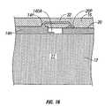
- FIG. 17depicts a flex circuitry prepared for use with an alternative embodiment that recesses semiconductor die in a window in the flex circuitry in accordance with an embodiment of the present invention.
- FIG. 18depicts a flex circuitry prepared for use with a recessed semiconductor die arrangement for an exemplar module in accordance with an embodiment of the present invention.
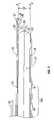
- FIG. 1is a side view of an exemplar module 10 devised in accordance with a preferred embodiment of the present invention.
- Exemplar module 10is comprised of leaded IC 12 and semiconductor die 14 each connected to flex circuitry 20 .
- leaded IC 12is a flash memory circuit and semiconductor die 14 is a controller.
- semiconductor die 14is covered by an encapsulate 16 as shown.
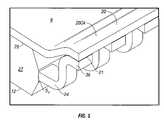
- FIG. 2is an enlarged side view of the area marked “A” in FIG. 1 of a module devised in accordance with a preferred embodiment of the present invention.
- leaded packaged IC 12has upper side 29 and lower side 25 and is connected to flex circuitry 20 through leads 24 that are connected to leaded circuit pads 21 along one side of flex circuitry 20 which is identified as side 11 in later views.
- Leads 24typically but not always, exhibit feet 36 . Later views will show embodiments in which leads 24 do not exhibit feet 36 .
- Leads 24may be connected to either or both of the sides of flex circuitry 20 as will be later shown.
- Module contacts 18 which comprise module array 18 Aare, in the depicted embodiment, pads such as those found in land grid array (LGA) but other types of module contacts 18 may be employed in embodiments of the present invention.
- LGAland grid array
- Body 27 of leaded packaged IC 12has a lower surface 25 that is in contact with flex circuitry 20 .
- “contact” between the lower surface 25 of leaded packaged IC 12 and the surface of flex circuit 20includes not only direct contact between lower surface or side 25 of leaded packaged IC 12 and the flex circuitry but shall include those instances where intermediate materials such as depicted adhesive 33 is used between the respective leaded packaged IC and flex circuitry.
- leaded packaged IC 12exhibits lateral sides S 1 and S 2 which, as those of skill will recognize, may be in the character of edges or sides and need not be perpendicular in aspect to the upper and lower surfaces 29 and 25 , respectively.
- Leads 24are emergent from sides S 1 and S 2 in the depicted leaded packaged IC 12 but those of skill will note that some leaded packaged ICs may have leads emergent from only one side or more than two sides.
- leads 24are configured within space SP defined by planes PL and PU which are defined by lower and upper surfaces 25 and 29 , respectively, of the leaded IC to allow the lower surface 25 of the leaded packaged IC 12 to be in contact with the flex circuitry 20 (either directly or indirectly) when leaded packaged IC 12 is connected to the flex.
- leads 24may be modified or reconfigured. This is preferably performed before mounting of the leaded IC to flex circuit 20 .
- a preferred method for reconfiguration of leads 24comprises use of a jig to fix the position of body 27 of the leaded packaged IC and, preferably, support the lead at the point of emergence from the body at sides S 1 and S 2 before deflection of the respective leads toward the upper plane PU to confine leads 24 to the space between planes PL and PU of the leaded packaged IC. This is because typically, leaded packaged ICs such as TSOPs are configured with leads that extend beyond the lower plane PL. In order for the lower surface 25 of the respective leaded packaged ICs to contact (either directly or through an adhesive or thermal intermediary, for example) the respective surfaces of the flex circuit, the leads 24 may need to be reconfigured.
- leads 24may not, however, require or exhibit configurations in which the lead is within space SP and yet lower surface 25 still exhibits contact with flex circuitry 20 .
- leaded packaged IC 12exhibits a straight lead 24 that penetrates flex circuitry 20 and is connected to both sides 9 and 11 of flex circuitry 20 with solder 35 .
- FIG. 4depicts an alternative embodiment in accord with the present invention in which flex circuitry 20 exhibits lead holes 22 through which leads 24 project so that leads 24 may be connected to leaded IC pads 21 which, in this instance, are on side 9 of flex circuitry 20 rather than side 11 as depicted in several other Figs. The result is that lower major surface 25 of leaded packaged IC 12 contacts flex circuitry 20 .
- FIG. 5depicts yet another technique for connection of leaded packaged IC 12 to flex circuitry 20 while realizing contact between lower surface 25 and flex circuitry 20 .
- an area 20 CA of flex circuitry 20is deflected to allow leads 24 and in particular, feet 36 of leads 24 to be connected to leaded IC pads 21 on side 11 of flex circuitry 20 .
- the resultis that lower surface 25 of leaded package IC 12 is in contact with flex circuitry 20 .
- FIG. 6depicts yet another technique for connecting leaded packaged IC 12 to flex circuitry 20 .
- leads 24penetrate deflected area 20 CA of flex circuitry 20 which, in this embodiment, is deflected toward the body 27 of leaded packaged IC 12 rather than away from leaded packaged IC 12 as shown in earlier FIG. 5 .
- leads 24are connected to both sides 9 and 11 of flex circuitry 20 .
- Leads 24are also parallel with lower major surface 25 as shown. Lower major surface 25 of leaded packaged IC is in contact with flex circuitry 20 and, in particular, with side 11 of flex circuitry 20 .
- FIG. 7depicts an alternative embodiment of the present invention in which flex circuitry 20 has distal ends 20 D that are deflected to contact inner side 24 I of leads 24 which has, as shown, an inner side 24 I and an external side 24 X.
- flex circuitry 20accomodates the configuration of leads 24 and lower surface 25 is in contact with flex circuitry 20 .
- FIG. 8is a perspective view of a module devised in accordance with an embodiment of the present invention.
- semiconductor die 14is connected through wire bonds 32 to flex circuit 20 .
- wire bonds 32are attached to flex pads 20 P along surface 9 of flex circuitry 20 .
- leaded packaged IC 12is connected to the other major side of flex circuitry 20 through leads 24 .
- FIG. 9is a side view of an exemplar module 10 devised in accordance with a preferred embodiment of the present invention.
- Die 14is shown encapsulated by encapsulate 16 .
- a variety of methodscan be employed to effectuate the encapsulation of die 14 and such methods are known to those of skill in the art.
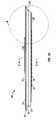
- FIG. 10depicts a major side 11 of flex circuitry 20 as employed in a preferred embodiment of the present invention.
- the plurality of leaded IC pads 21 shown along side 11 of flex circuitry 20provide contact sites for the leads 24 of leaded IC 12 .
- leaded IC pads 21need not be on side 11 of flex circuitry 20 if leads 24 reach side 9 of flex circuitry 20 as shown in an earlier Fig.
- Flex circuitry 20is preferably comprised from one or more conductive layers supported by one or more flexible substrate layers.
- the entirety of flex circuitry 20may be flexible or, as those of skill in the art will recognize, the flexible circuitry may be made flexible in certain areas and rigid in other areas such as those areas where leaded packaged IC 12 is mounted, for example.
- FIG. 11depicts major surface 9 of flex circuit 20 illustrating module contacts array 18 A and module contacts 18 as well as mounted semiconductor die 14 wire-bond connected to the plurality 20 A of flex pads 20 P.
- semiconductor die 14is depicted as being mounted on the surface of flex circuitry 20 .
- a later alternative embodimentis an example of an embodiment in which semiconductor die 14 is inset into a window in flex circuitry 20 .
- FIG. 12depicts an enlarged portion of a module 10 devised in accordance with a preferred embodiment.
- module contacts 18are illustrated as the commonly understood BGA type contacts often found along the surfaces of CSP devices. Other types of contacts may be employed as module contacts 18 .
- FIG. 13depicts a module 10 devised in accordance with an alternative embodiment in which semiconductor die 14 is set into a window in flex circuitry 20 .
- semiconductor die 14resided on flex circuit 20 .
- flex circuitry 20has a window into which is set semiconductor die 14 .
- die 14is not on the surface of flexible circuitry 20 and although it may be connected to either side of flexible circuitry 20 , it is shown in enlarged detail in FIG. 16 , for example, as being wire-bond connected to the upper surface of flexible circuitry 20 which corresponds to earlier identified major surface 9 of flexible circuitry 20 .
- semiconductor die 14is shown with a lower profile than depicted in earlier depictions of this disclosure.
- a semiconductor die that is inset into a window in flex circuitry 20will be identified as die 14 R which is, as shown, preferably encapsulated as shown to protect, for example, the wire bonds and the die.
- soldersuch as solder 35 shown in several of the preceding Figs., or other conductive attachment.
- Other forms of bonding other than solder between leaded IC pads 21 and leads 24may also be employed (such as brazing, welding, tab bonding, or ultrasonic bonding, just as examples) but soldering techniques are well understood and adapted for use in large scale manufacturing.
- FIG. 14is an enlarged depiction of a portion of module 10 identified in FIG. 13 with the letter “B”.
- Inset semiconductor die 14 Ris identified in encapsulate 16 while leaded packaged IC 12 is shown connected to flex circuitry 20 through leads 24 connected to leaded circuit pads 21 of flexible circuitry 20 while both the upper and lower surfaces 29 and 25 , respectively, of body 27 of leaded packaged IC 12 are preferably connected to flexible circuitry 20 through adhesive 33 .
- the identification of “upper” and “lower” surfaces or sides of leaded packaged IC 12is with reference to the normal orientation of the device and typically employed, but such oriented terms are not with reference to a relative “up” or “down” in the Figs. Those of skill will understand, therefore, that the identified upper side 29 is actually seen as being below the lower side 25 of leaded packaged IC 12 in the depiction of, for example, FIG. 14 when that depiction is viewed.
- FIG. 15depicts recessed semiconductor die 14 R and illustrates the plural die pads 14 P and plural flex pads 20 P and the wire bonds 32 that connect die 14 R to flex circuit 20 .
- Die attach 14 DAis also shown. As those of skill understand, die attach 14 DA is typically an adhesive.
- FIG. 16is an enlarged depiction showing a cross-sectional view along the line identified as C-C in earlier FIG. 13 .
- Body 27 of leaded packaged IC 12is shown supporting recessed semiconductor die 14 R which is attached to body 27 through die attach shown as 14 DA.
- Exemplar die pad 14 Pis connected to flex pad 20 P of flexible circuitry 20 through wire bond 32 .
- the entire connection areais preferable encapsulated with encapsulate 16 .
- FIG. 17depicts flex circuitry 20 prepared for use with an alternative embodiment that recesses semiconductor die 14 in a window W in the flex circuitry. Such constructions result in lower profiles for modules 10 . Leaded pads 21 are shown along side 11 of flexible circuitry 20 .
- FIG. 18depicts flex circuitry 20 prepared for use with a recessed semiconductor die arrangement for module 10 .
- Flexible circuitry pads 20 P along side 9 and array 18 A of module contacts 18are shown.
- Window Wprovides the space through which die 14 is disposed when a module 10 in accordance with an alternative embodiment is constructed.
- semiconductor die 14when semiconductor die 14 is recessed in a module 10 it is identified as die 14 R, while in those instances where die 14 resides on flex circuitry 20 , it is identified as semiconductor die 14 .
- a diecan be used in either mode, recessed in a window W of flex circuitry 20 or on the surface of flex circuitry 20 .
- the present inventionmay also be employed with circuitry other than or in addition to memory such as the flash memory depicted in a number of the present Figs.
- Other exemplar types of circuitry that may be aggregated in accordance with embodiments of the inventioninclude, just as non-limiting examples, DRAMs, FPGAs, and system stacks that include logic and memory as well as communications or graphics devices.
- the depicted profile for leaded packaged IC 12is not a limitation and that leaded packaged IC 12 does not have to be a TSOP or TSOP-like and the package employed may have more than one die or leads emergent from one, two, three or all sides of the respective package body.
- a module 10 in accordance with embodiments of the present inventionmay employ a leaded packaged IC 12 that has more than one die within the package and may exhibit leads emergent from only one side of the package.
Landscapes
- Engineering & Computer Science (AREA)
- Microelectronics & Electronic Packaging (AREA)
- Power Engineering (AREA)
- Physics & Mathematics (AREA)
- Condensed Matter Physics & Semiconductors (AREA)
- General Physics & Mathematics (AREA)
- Computer Hardware Design (AREA)
- Metallurgy (AREA)
- Manufacturing & Machinery (AREA)
- Semiconductor Memories (AREA)
Abstract
Description
Claims (27)
Priority Applications (7)
| Application Number | Priority Date | Filing Date | Title |
|---|---|---|---|
| US11/436,946US7508069B2 (en) | 2006-01-11 | 2006-05-18 | Managed memory component |
| US11/447,590US20070164416A1 (en) | 2006-01-17 | 2006-06-07 | Managed memory component |
| US11/482,325US20070158821A1 (en) | 2006-01-11 | 2006-07-07 | Managed memory component |
| US11/502,852US20070158811A1 (en) | 2006-01-11 | 2006-08-11 | Low profile managed memory component |
| PCT/US2007/064407WO2007136917A2 (en) | 2006-05-18 | 2007-03-20 | Managed memory component |
| PCT/US2007/065009WO2007136928A2 (en) | 2006-05-18 | 2007-03-27 | Low profile managed memory component |
| US12/395,984US20090160042A1 (en) | 2006-01-17 | 2009-03-02 | Managed Memory Component |
Applications Claiming Priority (2)
| Application Number | Priority Date | Filing Date | Title |
|---|---|---|---|
| US11/330,307US7508058B2 (en) | 2006-01-11 | 2006-01-11 | Stacked integrated circuit module |
| US11/436,946US7508069B2 (en) | 2006-01-11 | 2006-05-18 | Managed memory component |
Related Parent Applications (1)
| Application Number | Title | Priority Date | Filing Date |
|---|---|---|---|
| US11/330,307Continuation-In-PartUS7508058B2 (en) | 2006-01-11 | 2006-01-11 | Stacked integrated circuit module |
Related Child Applications (2)
| Application Number | Title | Priority Date | Filing Date |
|---|---|---|---|
| US11/330,307Continuation-In-PartUS7508058B2 (en) | 2006-01-11 | 2006-01-11 | Stacked integrated circuit module |
| US11/332,307Continuation-In-PartUS7584357B2 (en) | 2005-01-27 | 2006-01-17 | Control device for creating one-time password using pre-input button code, home server for authenticating control device using one-time password, and method for authenticating control device with one-time password |
Publications (2)
| Publication Number | Publication Date |
|---|---|
| US20070159545A1 US20070159545A1 (en) | 2007-07-12 |
| US7508069B2true US7508069B2 (en) | 2009-03-24 |
Family
ID=38232033
Family Applications (1)
| Application Number | Title | Priority Date | Filing Date |
|---|---|---|---|
| US11/436,946Active2027-03-12US7508069B2 (en) | 2006-01-11 | 2006-05-18 | Managed memory component |
Country Status (1)
| Country | Link |
|---|---|
| US (1) | US7508069B2 (en) |
Cited By (1)
| Publication number | Priority date | Publication date | Assignee | Title |
|---|---|---|---|---|
| US8954948B2 (en) | 2011-06-17 | 2015-02-10 | Bae Systems Controls Inc. | Obsolescence tolerant flash memory architecture and physical building block (PBB) implementation |
Citations (365)
| Publication number | Priority date | Publication date | Assignee | Title |
|---|---|---|---|---|
| US3436604A (en) | 1966-04-25 | 1969-04-01 | Texas Instruments Inc | Complex integrated circuit array and method for fabricating same |
| US3654394A (en) | 1969-07-08 | 1972-04-04 | Gordon Eng Co | Field effect transistor switch, particularly for multiplexing |
| US3704455A (en) | 1971-02-01 | 1972-11-28 | Alfred D Scarbrough | 3d-coaxial memory construction and method of making |
| US3746934A (en) | 1971-05-06 | 1973-07-17 | Siemens Ag | Stack arrangement of semiconductor chips |
| US3766439A (en) | 1972-01-12 | 1973-10-16 | Gen Electric | Electronic module using flexible printed circuit board with heat sink means |
| US3772776A (en) | 1969-12-03 | 1973-11-20 | Thomas & Betts Corp | Method of interconnecting memory plane boards |
| US3983547A (en) | 1974-06-27 | 1976-09-28 | International Business Machines - Ibm | Three-dimensional bubble device |
| US4288841A (en) | 1979-09-20 | 1981-09-08 | Bell Telephone Laboratories, Incorporated | Double cavity semiconductor chip carrier |
| US4398235A (en) | 1980-09-11 | 1983-08-09 | General Motors Corporation | Vertical integrated circuit package integration |
| US4406508A (en) | 1981-07-02 | 1983-09-27 | Thomas & Betts Corporation | Dual-in-line package assembly |
| US4437235A (en) | 1980-12-29 | 1984-03-20 | Honeywell Information Systems Inc. | Integrated circuit package |
| US4513368A (en) | 1981-05-22 | 1985-04-23 | Data General Corporation | Digital data processing system having object-based logical memory addressing and self-structuring modular memory |
| US4567543A (en) | 1983-02-15 | 1986-01-28 | Motorola, Inc. | Double-sided flexible electronic circuit module |
| US4587596A (en) | 1984-04-09 | 1986-05-06 | Amp Incorporated | High density mother/daughter circuit board connector |
| US4645944A (en) | 1983-09-05 | 1987-02-24 | Matsushita Electric Industrial Co., Ltd. | MOS register for selecting among various data inputs |
| US4656605A (en) | 1983-09-02 | 1987-04-07 | Wang Laboratories, Inc. | Single in-line memory module |
| US4682207A (en) | 1982-03-17 | 1987-07-21 | Fujitsu Limited | Semiconductor device including leadless packages and a base plate for mounting the leadless packages |
| US4696525A (en) | 1985-12-13 | 1987-09-29 | Amp Incorporated | Socket for stacking integrated circuit packages |
| US4709300A (en) | 1986-05-05 | 1987-11-24 | Itt Gallium Arsenide Technology Center, A Division Of Itt Corporation | Jumper for a semiconductor assembly |
| US4733461A (en) | 1984-12-28 | 1988-03-29 | Micro Co., Ltd. | Method of stacking printed circuit boards |
| US4758875A (en) | 1981-04-30 | 1988-07-19 | Hitachi, Ltd. | Resin encapsulated semiconductor device |
| US4763188A (en) | 1986-08-08 | 1988-08-09 | Thomas Johnson | Packaging system for multiple semiconductor devices |
| US4821007A (en) | 1987-02-06 | 1989-04-11 | Tektronix, Inc. | Strip line circuit component and method of manufacture |
| US4823234A (en) | 1985-08-16 | 1989-04-18 | Dai-Ichi Seiko Co., Ltd. | Semiconductor device and its manufacture |
| US4833568A (en) | 1988-01-29 | 1989-05-23 | Berhold G Mark | Three-dimensional circuit component assembly and method corresponding thereto |
| US4850892A (en) | 1985-12-16 | 1989-07-25 | Wang Laboratories, Inc. | Connecting apparatus for electrically connecting memory modules to a printed circuit board |
| US4862249A (en) | 1987-04-17 | 1989-08-29 | Xoc Devices, Inc. | Packaging system for stacking integrated circuits |
| US4884237A (en) | 1984-03-28 | 1989-11-28 | International Business Machines Corporation | Stacked double density memory module using industry standard memory chips |
| US4891789A (en) | 1988-03-03 | 1990-01-02 | Bull Hn Information Systems, Inc. | Surface mounted multilayer memory printed circuit board |
| US4894706A (en) | 1985-02-14 | 1990-01-16 | Nippon Telegraph And Telephone Corporation | Three-dimensional packaging of semiconductor device chips |
| US4911643A (en) | 1988-10-11 | 1990-03-27 | Beta Phase, Inc. | High density and high signal integrity connector |
| US4953060A (en) | 1989-05-05 | 1990-08-28 | Ncr Corporation | Stackable integrated circuit chip package with improved heat removal |
| US4956694A (en) | 1988-11-04 | 1990-09-11 | Dense-Pac Microsystems, Inc. | Integrated circuit chip stacking |
| US4972580A (en) | 1988-06-24 | 1990-11-27 | Kabushiki Kaisha Toshiba | Method for connecting electronic components with dummy patterns |
| US4982265A (en) | 1987-06-24 | 1991-01-01 | Hitachi, Ltd. | Semiconductor integrated circuit device and method of manufacturing the same |
| US4983533A (en) | 1987-10-28 | 1991-01-08 | Irvine Sensors Corporation | High-density electronic modules - process and product |
| US4985703A (en) | 1988-02-03 | 1991-01-15 | Nec Corporation | Analog multiplexer |
| US5012323A (en) | 1989-11-20 | 1991-04-30 | Micron Technology, Inc. | Double-die semiconductor package having a back-bonded die and a face-bonded die interconnected on a single leadframe |
| US5016138A (en) | 1987-10-27 | 1991-05-14 | Woodman John K | Three dimensional integrated circuit package |
| US5025306A (en) | 1988-08-09 | 1991-06-18 | Texas Instruments Incorporated | Assembly of semiconductor chips |
| US5034350A (en) | 1987-09-23 | 1991-07-23 | Sgs Thomson Microelectronics S.R.L. | Semiconductor device package with dies mounted on both sides of the central pad of a metal frame |
| US5041015A (en) | 1990-03-30 | 1991-08-20 | Cal Flex, Inc. | Electrical jumper assembly |
| US5050039A (en) | 1990-06-26 | 1991-09-17 | Digital Equipment Corporation | Multiple circuit chip mounting and cooling arrangement |
| US5053853A (en) | 1990-05-08 | 1991-10-01 | International Business Machines Corporation | Modular electronic packaging system |
| US5065277A (en) | 1990-07-13 | 1991-11-12 | Sun Microsystems, Inc. | Three dimensional packaging arrangement for computer systems and the like |
| US5081067A (en) | 1989-02-10 | 1992-01-14 | Fujitsu Limited | Ceramic package type semiconductor device and method of assembling the same |
| US5099393A (en) | 1991-03-25 | 1992-03-24 | International Business Machines Corporation | Electronic package for high density applications |
| US5104820A (en) | 1989-07-07 | 1992-04-14 | Irvine Sensors Corporation | Method of fabricating electronic circuitry unit containing stacked IC layers having lead rerouting |
| US5117282A (en) | 1990-10-29 | 1992-05-26 | Harris Corporation | Stacked configuration for integrated circuit devices |
| US5122862A (en) | 1989-03-15 | 1992-06-16 | Ngk Insulators, Ltd. | Ceramic lid for sealing semiconductor element and method of manufacturing the same |
| US5138430A (en) | 1991-06-06 | 1992-08-11 | International Business Machines Corporation | High performance versatile thermally enhanced IC chip mounting |
| US5140405A (en) | 1990-08-30 | 1992-08-18 | Micron Technology, Inc. | Semiconductor assembly utilizing elastomeric single axis conductive interconnect |
| US5159434A (en) | 1990-02-01 | 1992-10-27 | Hitachi, Ltd. | Semiconductor device having a particular chip pad structure |
| US5159535A (en) | 1987-03-11 | 1992-10-27 | International Business Machines Corporation | Method and apparatus for mounting a flexible film semiconductor chip carrier on a circuitized substrate |
| US5191404A (en) | 1989-12-20 | 1993-03-02 | Digital Equipment Corporation | High density memory array packaging |
| US5198888A (en) | 1987-12-28 | 1993-03-30 | Hitachi, Ltd. | Semiconductor stacked device |
| US5198965A (en) | 1991-12-18 | 1993-03-30 | International Business Machines Corporation | Free form packaging of specific functions within a computer system |
| US5208729A (en) | 1992-02-14 | 1993-05-04 | International Business Machines Corporation | Multi-chip module |
| US5219794A (en) | 1991-03-14 | 1993-06-15 | Hitachi, Ltd. | Semiconductor integrated circuit device and method of fabricating same |
| US5222014A (en) | 1992-03-02 | 1993-06-22 | Motorola, Inc. | Three-dimensional multi-chip pad array carrier |
| US5224023A (en) | 1992-02-10 | 1993-06-29 | Smith Gary W | Foldable electronic assembly module |
| US5229916A (en) | 1992-03-04 | 1993-07-20 | International Business Machines Corporation | Chip edge interconnect overlay element |
| US5229917A (en) | 1992-07-24 | 1993-07-20 | The United States Of America As Represented By The Secretary Of The Air Force | VLSI integration into a 3-D WSI dual composite module |
| US5239198A (en) | 1989-09-06 | 1993-08-24 | Motorola, Inc. | Overmolded semiconductor device having solder ball and edge lead connective structure |
| US5241456A (en) | 1990-07-02 | 1993-08-31 | General Electric Company | Compact high density interconnect structure |
| US5241454A (en) | 1992-01-22 | 1993-08-31 | International Business Machines Corporation | Mutlilayered flexible circuit package |
| US5243133A (en) | 1992-02-18 | 1993-09-07 | International Business Machines, Inc. | Ceramic chip carrier with lead frame or edge clip |
| US5247423A (en) | 1992-05-26 | 1993-09-21 | Motorola, Inc. | Stacking three dimensional leadless multi-chip module and method for making the same |
| US5253010A (en) | 1988-05-13 | 1993-10-12 | Minolta Camera Kabushiki Kaisha | Printed circuit board |
| US5252857A (en) | 1991-08-05 | 1993-10-12 | International Business Machines Corporation | Stacked DCA memory chips |
| US5259770A (en) | 1992-03-19 | 1993-11-09 | Amp Incorporated | Impedance controlled elastomeric connector |
| US5261068A (en) | 1990-05-25 | 1993-11-09 | Dell Usa L.P. | Dual path memory retrieval system for an interleaved dynamic RAM memory unit |
| US5262927A (en) | 1992-02-07 | 1993-11-16 | Lsi Logic Corporation | Partially-molded, PCB chip carrier package |
| US5268815A (en) | 1992-02-14 | 1993-12-07 | International Business Machines Corporation | High density, high performance memory circuit package |
| US5276418A (en) | 1988-11-16 | 1994-01-04 | Motorola, Inc. | Flexible substrate electronic assembly |
| US5279029A (en) | 1990-08-01 | 1994-01-18 | Staktek Corporation | Ultra high density integrated circuit packages method |
| US5281852A (en) | 1991-12-10 | 1994-01-25 | Normington Peter J C | Semiconductor device including stacked die |
| US5289062A (en) | 1991-03-18 | 1994-02-22 | Quality Semiconductor, Inc. | Fast transmission gate switch |
| US5289346A (en) | 1991-02-26 | 1994-02-22 | Microelectronics And Computer Technology Corporation | Peripheral to area adapter with protective bumper for an integrated circuit chip |
| US5311401A (en) | 1991-07-09 | 1994-05-10 | Hughes Aircraft Company | Stacked chip assembly and manufacturing method therefor |
| US5313097A (en) | 1992-11-16 | 1994-05-17 | International Business Machines, Corp. | High density memory module |
| US5313096A (en) | 1992-03-16 | 1994-05-17 | Dense-Pac Microsystems, Inc. | IC chip package having chip attached to and wire bonded within an overlying substrate |
| US5343075A (en) | 1991-06-29 | 1994-08-30 | Sony Corporation | Composite stacked semiconductor device with contact plates |
| US5345205A (en) | 1990-04-05 | 1994-09-06 | General Electric Company | Compact high density interconnected microwave system |
| US5347428A (en) | 1992-12-03 | 1994-09-13 | Irvine Sensors Corporation | Module comprising IC memory stack dedicated to and structurally combined with an IC microprocessor chip |
| US5361228A (en) | 1992-04-30 | 1994-11-01 | Fuji Photo Film Co., Ltd. | IC memory card system having a common data and address bus |
| US5375041A (en) | 1992-12-02 | 1994-12-20 | Intel Corporation | Ra-tab array bump tab tape based I.C. package |
| US5377077A (en) | 1990-08-01 | 1994-12-27 | Staktek Corporation | Ultra high density integrated circuit packages method and apparatus |
| US5386341A (en) | 1993-11-01 | 1995-01-31 | Motorola, Inc. | Flexible substrate folded in a U-shape with a rigidizer plate located in the notch of the U-shape |
| US5390844A (en) | 1993-07-23 | 1995-02-21 | Tessera, Inc. | Semiconductor inner lead bonding tool |
| US5394303A (en) | 1992-09-11 | 1995-02-28 | Kabushiki Kaisha Toshiba | Semiconductor device |
| US5394010A (en) | 1991-03-13 | 1995-02-28 | Kabushiki Kaisha Toshiba | Semiconductor assembly having laminated semiconductor devices |
| US5394300A (en) | 1992-09-04 | 1995-02-28 | Mitsubishi Denki Kabushiki Kaisha | Thin multilayered IC memory card |
| US5397916A (en) | 1991-12-10 | 1995-03-14 | Normington; Peter J. C. | Semiconductor device including stacked die |
| US5400003A (en) | 1992-08-19 | 1995-03-21 | Micron Technology, Inc. | Inherently impedance matched integrated circuit module |
| US5402006A (en) | 1992-11-10 | 1995-03-28 | Texas Instruments Incorporated | Semiconductor device with enhanced adhesion between heat spreader and leads and plastic mold compound |
| US5422435A (en) | 1992-05-22 | 1995-06-06 | National Semiconductor Corporation | Stacked multi-chip modules and method of manufacturing |
| US5428190A (en) | 1993-07-02 | 1995-06-27 | Sheldahl, Inc. | Rigid-flex board with anisotropic interconnect and method of manufacture |
| US5438224A (en) | 1992-04-23 | 1995-08-01 | Motorola, Inc. | Integrated circuit package having a face-to-face IC chip arrangement |
| US5446620A (en) | 1990-08-01 | 1995-08-29 | Staktek Corporation | Ultra high density integrated circuit packages |
| US5448511A (en) | 1994-06-01 | 1995-09-05 | Storage Technology Corporation | Memory stack with an integrated interconnect and mounting structure |
| US5455740A (en) | 1994-03-07 | 1995-10-03 | Staktek Corporation | Bus communication system for stacked high density integrated circuit packages |
| US5475920A (en) | 1990-08-01 | 1995-12-19 | Burns; Carmen D. | Method of assembling ultra high density integrated circuit packages |
| US5477082A (en) | 1994-01-11 | 1995-12-19 | Exponential Technology, Inc. | Bi-planar multi-chip module |
| US5484959A (en) | 1992-12-11 | 1996-01-16 | Staktek Corporation | High density lead-on-package fabrication method and apparatus |
| US5491612A (en) | 1995-02-21 | 1996-02-13 | Fairchild Space And Defense Corporation | Three-dimensional modular assembly of integrated circuits |
| US5499160A (en) | 1990-08-01 | 1996-03-12 | Staktek Corporation | High density integrated circuit module with snap-on rail assemblies |
| US5502333A (en) | 1994-03-30 | 1996-03-26 | International Business Machines Corporation | Semiconductor stack structures and fabrication/sparing methods utilizing programmable spare circuit |
| US5514907A (en) | 1995-03-21 | 1996-05-07 | Simple Technology Incorporated | Apparatus for stacking semiconductor chips |
| US5523695A (en) | 1994-08-26 | 1996-06-04 | Vlsi Technology, Inc. | Universal test socket for exposing the active surface of an integrated circuit in a die-down package |
| US5523619A (en) | 1993-11-03 | 1996-06-04 | International Business Machines Corporation | High density memory structure |
| US5548091A (en) | 1993-10-26 | 1996-08-20 | Tessera, Inc. | Semiconductor chip connection components with adhesives and methods for bonding to the chip |
| US5552631A (en) | 1992-06-04 | 1996-09-03 | Lsi Logic Corporation | Semiconductor device assembly including power or ground plane which is provided on opposite surface of insulating layer from signal traces, and is exposed to central opening in insulating layer for interconnection to semiconductor die |
| US5572065A (en) | 1992-06-26 | 1996-11-05 | Staktek Corporation | Hermetically sealed ceramic integrated circuit heat dissipating package |
| US5579207A (en) | 1994-10-20 | 1996-11-26 | Hughes Electronics | Three-dimensional integrated circuit stacking |
| US5588205A (en) | 1995-01-24 | 1996-12-31 | Staktek Corporation | Method of manufacturing a high density integrated circuit module having complex electrical interconnect rails |
| US5592364A (en) | 1995-01-24 | 1997-01-07 | Staktek Corporation | High density integrated circuit module with complex electrical interconnect rails |
| US5594275A (en) | 1993-11-18 | 1997-01-14 | Samsung Electronics Co., Ltd. | J-leaded semiconductor package having a plurality of stacked ball grid array packages |
| US5600541A (en) | 1993-12-08 | 1997-02-04 | Hughes Aircraft Company | Vertical IC chip stack with discrete chip carriers formed from dielectric tape |
| US5612570A (en) | 1995-04-13 | 1997-03-18 | Dense-Pac Microsystems, Inc. | Chip stack and method of making same |
| US5625221A (en) | 1994-03-03 | 1997-04-29 | Samsung Electronics Co., Ltd. | Semiconductor assembly for a three-dimensional integrated circuit package |
| US5631807A (en) | 1995-01-20 | 1997-05-20 | Minnesota Mining And Manufacturing Company | Electronic circuit structure with aperture suspended component |
| US5642055A (en) | 1990-02-14 | 1997-06-24 | Particle Interconnect, Inc. | Electrical interconnect using particle enhanced joining of metal surfaces |
| US5644161A (en) | 1993-03-29 | 1997-07-01 | Staktek Corporation | Ultra-high density warp-resistant memory module |
| US5646446A (en) | 1995-12-22 | 1997-07-08 | Fairchild Space And Defense Corporation | Three-dimensional flexible assembly of integrated circuits |
| US5654877A (en) | 1991-08-15 | 1997-08-05 | Staktek Corporation | Lead-on-chip integrated circuit apparatus |
| US5657537A (en) | 1995-05-30 | 1997-08-19 | General Electric Company | Method for fabricating a stack of two dimensional circuit modules |
| US5659952A (en) | 1994-09-20 | 1997-08-26 | Tessera, Inc. | Method of fabricating compliant interface for semiconductor chip |
| US5677566A (en) | 1995-05-08 | 1997-10-14 | Micron Technology, Inc. | Semiconductor chip package |
| US5677569A (en) | 1994-10-27 | 1997-10-14 | Samsung Electronics Co., Ltd. | Semiconductor multi-package stack |
| US5714802A (en) | 1991-06-18 | 1998-02-03 | Micron Technology, Inc. | High-density electronic module |
| US5715144A (en) | 1994-12-30 | 1998-02-03 | International Business Machines Corporation | Multi-layer, multi-chip pyramid and circuit board structure |
| US5729894A (en) | 1992-07-21 | 1998-03-24 | Lsi Logic Corporation | Method of assembling ball bump grid array semiconductor packages |
| US5744862A (en) | 1996-03-29 | 1998-04-28 | Mitsubishi Denki Kabushiki Kaisha | Reduced thickness semiconductor device with IC packages mounted in openings on substrate |
| US5751553A (en) | 1992-09-16 | 1998-05-12 | Clayton; James E. | Thin multichip module including a connector frame socket having first and second apertures |
| US5754409A (en) | 1996-11-06 | 1998-05-19 | Dynamem, Inc. | Foldable electronic assembly module |
| US5764497A (en) | 1995-11-13 | 1998-06-09 | Minolta Co, Ltd. | Circuit board connection method and connection structure |
| US5778552A (en) | 1995-05-08 | 1998-07-14 | Renishaw Plc | Touch sensor |
| US5778522A (en) | 1996-05-20 | 1998-07-14 | Staktek Corporation | Method of manufacturing a high density integrated circuit module with complex electrical interconnect rails having electrical interconnect strain relief |
| US5783464A (en) | 1992-06-26 | 1998-07-21 | Staktek Corporation | Method of forming a hermetically sealed circuit lead-on package |
| US5789815A (en) | 1996-04-23 | 1998-08-04 | Motorola, Inc. | Three dimensional semiconductor package having flexible appendages |
| US5801439A (en) | 1994-04-20 | 1998-09-01 | Fujitsu Limited | Semiconductor device and semiconductor device unit for a stack arrangement |
| US5801437A (en) | 1993-03-29 | 1998-09-01 | Staktek Corporation | Three-dimensional warp-resistant integrated circuit module method and apparatus |
| US5805424A (en) | 1996-09-24 | 1998-09-08 | Texas Instruments Incorporated | Microelectronic assemblies including Z-axis conductive films |
| US5805422A (en) | 1994-09-21 | 1998-09-08 | Nec Corporation | Semiconductor package with flexible board and method of fabricating the same |
| US5811879A (en) | 1996-06-26 | 1998-09-22 | Micron Technology, Inc. | Stacked leads-over-chip multi-chip module |
| US5835988A (en) | 1996-03-27 | 1998-11-10 | Mitsubishi Denki Kabushiki Kaisha | Packed semiconductor device with wrap around external leads |
| US5844168A (en) | 1995-08-01 | 1998-12-01 | Minnesota Mining And Manufacturing Company | Multi-layer interconnect sutructure for ball grid arrays |
| US5861666A (en) | 1995-08-30 | 1999-01-19 | Tessera, Inc. | Stacked chip assembly |
| US5869353A (en) | 1997-11-17 | 1999-02-09 | Dense-Pac Microsystems, Inc. | Modular panel stacking process |
| US5899705A (en) | 1997-11-20 | 1999-05-04 | Akram; Salman | Stacked leads-over chip multi-chip module |
| US5917242A (en) | 1996-05-20 | 1999-06-29 | Micron Technology, Inc. | Combination of semiconductor interconnect |
| US5917709A (en) | 1997-06-16 | 1999-06-29 | Eastman Kodak Company | Multiple circuit board assembly having an interconnect mechanism that includes a flex connector |
| US5926369A (en) | 1998-01-22 | 1999-07-20 | International Business Machines Corporation | Vertically integrated multi-chip circuit package with heat-sink support |
| US5925934A (en) | 1995-10-28 | 1999-07-20 | Institute Of Microelectronics | Low cost and highly reliable chip-sized package |
| US5949657A (en) | 1997-12-01 | 1999-09-07 | Karabatsos; Chris | Bottom or top jumpered foldable electronic assembly |
| US5953214A (en) | 1994-03-07 | 1999-09-14 | International Business Machines Corporation | Dual substrate package assembly coupled to a conducting member |
| US5953215A (en) | 1997-12-01 | 1999-09-14 | Karabatsos; Chris | Apparatus and method for improving computer memory speed and capacity |
| US5959839A (en) | 1997-01-02 | 1999-09-28 | At&T Corp | Apparatus for heat removal using a flexible backplane |
| US5963427A (en) | 1997-12-11 | 1999-10-05 | Sun Microsystems, Inc. | Multi-chip module with flexible circuit board |
| US5973395A (en) | 1996-04-30 | 1999-10-26 | Yamaichi Electronics Co., Ltd. | IC package having a single wiring sheet with a lead pattern disposed thereon |
| US5977640A (en) | 1998-06-26 | 1999-11-02 | International Business Machines Corporation | Highly integrated chip-on-chip packaging |
| US5995370A (en) | 1997-09-01 | 1999-11-30 | Sharp Kabushiki Kaisha | Heat-sinking arrangement for circuit elements |
| US6002167A (en) | 1995-09-22 | 1999-12-14 | Hitachi Cable, Ltd. | Semiconductor device having lead on chip structure |
| US6002589A (en) | 1997-07-21 | 1999-12-14 | Rambus Inc. | Integrated circuit package for coupling to a printed circuit board |
| US6013948A (en) | 1995-11-27 | 2000-01-11 | Micron Technology, Inc. | Stackable chip scale semiconductor package with mating contacts on opposed surfaces |
| US6014316A (en) | 1997-06-13 | 2000-01-11 | Irvine Sensors Corporation | IC stack utilizing BGA contacts |
| US6021048A (en) | 1998-02-17 | 2000-02-01 | Smith; Gary W. | High speed memory module |
| US6025642A (en) | 1995-08-17 | 2000-02-15 | Staktek Corporation | Ultra high density integrated circuit packages |
| US6028352A (en) | 1997-06-13 | 2000-02-22 | Irvine Sensors Corporation | IC stack utilizing secondary leadframes |
| US6028365A (en) | 1998-03-30 | 2000-02-22 | Micron Technology, Inc. | Integrated circuit package and method of fabrication |
| US6028358A (en) | 1996-05-30 | 2000-02-22 | Nec Corporation | Package for a semiconductor device and a semiconductor device |
| US6030856A (en) | 1996-06-10 | 2000-02-29 | Tessera, Inc. | Bondable compliant pads for packaging of a semiconductor chip and method therefor |
| US6034878A (en) | 1996-12-16 | 2000-03-07 | Hitachi, Ltd. | Source-clock-synchronized memory system and memory unit |
| US6040624A (en) | 1997-10-02 | 2000-03-21 | Motorola, Inc. | Semiconductor device package and method |
| US6072233A (en) | 1998-05-04 | 2000-06-06 | Micron Technology, Inc. | Stackable ball grid array package |
| US6084293A (en) | 1997-07-25 | 2000-07-04 | Oki Electric Industry Co., Ltd. | Stacked semiconductor device |
| US6084778A (en) | 1997-04-29 | 2000-07-04 | Texas Instruments Incorporated | Three dimensional assembly using flexible wiring board |
| US6084294A (en) | 1998-08-26 | 2000-07-04 | Mitsubishi Denki Kabushiki Kaisha | Semiconductor device comprising stacked semiconductor elements |
| US6097087A (en) | 1997-10-31 | 2000-08-01 | Micron Technology, Inc. | Semiconductor package including flex circuit, interconnects and dense array external contacts |
| US6121676A (en) | 1996-12-13 | 2000-09-19 | Tessera, Inc. | Stacked microelectronic assembly and method therefor |
| US6133640A (en) | 1997-04-04 | 2000-10-17 | Elm Technology Corporation | Three-dimensional structure memory |
| US6137164A (en) | 1998-03-16 | 2000-10-24 | Texas Instruments Incorporated | Thin stacked integrated circuit device |
| US6157541A (en) | 1997-12-30 | 2000-12-05 | Siemens Aktiengesellschaft | Stack arrangement for two semiconductor memory chips and printed board for accepting a plurality of such stack arrangements |
| US6166443A (en) | 1998-04-30 | 2000-12-26 | Nec Corporation | Semiconductor device with reduced thickness |
| US6172418B1 (en) | 1998-06-24 | 2001-01-09 | Nec Corporation | Semiconductor device and method for fabricating the same |
| US6172874B1 (en) | 1998-04-06 | 2001-01-09 | Silicon Graphics, Inc. | System for stacking of integrated circuit packages |
| US6180881B1 (en) | 1998-05-05 | 2001-01-30 | Harlan Ruben Isaak | Chip stack and method of making same |
| US6187652B1 (en) | 1998-09-14 | 2001-02-13 | Fujitsu Limited | Method of fabrication of multiple-layer high density substrate |
| US6208521B1 (en) | 1997-05-19 | 2001-03-27 | Nitto Denko Corporation | Film carrier and laminate type mounting structure using same |
| US6205654B1 (en) | 1992-12-11 | 2001-03-27 | Staktek Group L.P. | Method of manufacturing a surface mount package |
| US6214641B1 (en) | 1996-06-25 | 2001-04-10 | Micron Technology, Inc. | Method of fabricating a multi-chip module |
| US6222737B1 (en) | 1999-04-23 | 2001-04-24 | Dense-Pac Microsystems, Inc. | Universal package and method of forming the same |
| US6222739B1 (en) | 1998-01-20 | 2001-04-24 | Viking Components | High-density computer module with stacked parallel-plane packaging |
| US6225688B1 (en) | 1997-12-11 | 2001-05-01 | Tessera, Inc. | Stacked microelectronic assembly and method therefor |
| US6233650B1 (en) | 1998-04-01 | 2001-05-15 | Intel Corporation | Using FET switches for large memory arrays |
| US6234820B1 (en) | 1997-07-21 | 2001-05-22 | Rambus Inc. | Method and apparatus for joining printed circuit boards |
| US6239496B1 (en) | 1999-01-18 | 2001-05-29 | Kabushiki Kaisha Toshiba | Package having very thin semiconductor chip, multichip module assembled by the package, and method for manufacturing the same |
| US6262895B1 (en) | 2000-01-13 | 2001-07-17 | John A. Forthun | Stackable chip package with flex carrier |
| US6262476B1 (en) | 1998-07-27 | 2001-07-17 | Siemens Aktiengesellschaft | Composite member composed of at least two integrated circuits and method for the manufacture of a composite member composed of at least two integrated circuits |
| US6265660B1 (en) | 1997-07-09 | 2001-07-24 | Micron Technology, Inc. | Package stack via bottom leaded plastic (BLP) packaging |
| US6265766B1 (en) | 1995-12-19 | 2001-07-24 | Micron Technology, Inc. | Flip chip adaptor package for bare die |
| US6266252B1 (en) | 1997-12-01 | 2001-07-24 | Chris Karabatsos | Apparatus and method for terminating a computer memory bus |
| US20010013423A1 (en) | 1996-10-31 | 2001-08-16 | Hormazdyar M. Dalal | Flip chip attach on flexible circuit carrier using chip with metallic cap on solder |
| US6281577B1 (en) | 1996-06-28 | 2001-08-28 | Pac Tech-Packaging Technologies Gmbh | Chips arranged in plurality of planes and electrically connected to one another |
| US6288924B1 (en) | 1996-02-26 | 2001-09-11 | Hitachi, Ltd. | Semiconductor device and process for manufacturing the same |
| US6300679B1 (en) | 1998-06-01 | 2001-10-09 | Semiconductor Components Industries, Llc | Flexible substrate for packaging a semiconductor component |
| US6303981B1 (en) | 1999-09-01 | 2001-10-16 | Micron Technology, Inc. | Semiconductor package having stacked dice and leadframes and method of fabrication |
| US6303997B1 (en) | 1998-04-08 | 2001-10-16 | Anam Semiconductor, Inc. | Thin, stackable semiconductor packages |
| US6310392B1 (en) | 1998-12-28 | 2001-10-30 | Staktek Group, L.P. | Stacked micro ball grid array packages |
| US6313522B1 (en) | 1998-08-28 | 2001-11-06 | Micron Technology, Inc. | Semiconductor structure having stacked semiconductor devices |
| US6313998B1 (en) | 1999-04-02 | 2001-11-06 | Legacy Electronics, Inc. | Circuit board assembly having a three dimensional array of integrated circuit packages |
| US6316825B1 (en) | 1998-05-15 | 2001-11-13 | Hyundai Electronics Industries Co., Ltd. | Chip stack package utilizing a connecting hole to improve electrical connection between leadframes |
| US6316838B1 (en) | 1999-10-29 | 2001-11-13 | Fujitsu Limited | Semiconductor device |
| US20010040793A1 (en) | 2000-02-01 | 2001-11-15 | Tetsuya Inaba | Electronic device and method of producing the same |
| US6323060B1 (en) | 1999-05-05 | 2001-11-27 | Dense-Pac Microsystems, Inc. | Stackable flex circuit IC package and method of making same |
| US6329708B1 (en) | 1999-04-26 | 2001-12-11 | Oki Electric Industry Co. Ltd. | Micro ball grid array semiconductor device and semiconductor module |
| US6329713B1 (en) | 1998-10-21 | 2001-12-11 | International Business Machines Corporation | Integrated circuit chip carrier assembly comprising a stiffener attached to a dielectric substrate |
| US6336262B1 (en) | 1996-10-31 | 2002-01-08 | International Business Machines Corporation | Process of forming a capacitor with multi-level interconnection technology |
| US6339254B1 (en) | 1998-09-01 | 2002-01-15 | Texas Instruments Incorporated | Stacked flip-chip integrated circuit assemblage |
| US20020006032A1 (en) | 2000-05-23 | 2002-01-17 | Chris Karabatsos | Low-profile registered DIMM |
| US6351029B1 (en) | 1999-05-05 | 2002-02-26 | Harlan R. Isaak | Stackable flex circuit chip package and method of making same |
| US6376769B1 (en) | 1999-05-18 | 2002-04-23 | Amerasia International Technology, Inc. | High-density electronic package, and method for making same |
| US6388333B1 (en) | 1999-11-30 | 2002-05-14 | Fujitsu Limited | Semiconductor device having protruding electrodes higher than a sealed portion |
| US6392953B2 (en) | 1996-11-19 | 2002-05-21 | Matsushita Electronics Corporation | Semiconductor memory |
| US6392162B1 (en) | 2000-11-10 | 2002-05-21 | Chris Karabatsos | Double-sided flexible jumper assembly and method of manufacture |
| US6404049B1 (en) | 1995-11-28 | 2002-06-11 | Hitachi, Ltd. | Semiconductor device, manufacturing method thereof and mounting board |
| US6404043B1 (en) | 2000-06-21 | 2002-06-11 | Dense-Pac Microsystems, Inc. | Panel stacking of BGA devices to form three-dimensional modules |
| US6410857B1 (en) | 2001-03-01 | 2002-06-25 | Lockheed Martin Corporation | Signal cross-over interconnect for a double-sided circuit card assembly |
| US6414384B1 (en) | 2000-12-22 | 2002-07-02 | Silicon Precision Industries Co., Ltd. | Package structure stacking chips on front surface and back surface of substrate |
| US6428360B2 (en) | 1999-04-16 | 2002-08-06 | Sun Microsystems, Inc. | Memory module with offset notches for improved insertion and stability and memory module connector |
| US6433418B1 (en) | 1998-07-24 | 2002-08-13 | Fujitsu Limited | Apparatus for a vertically accumulable semiconductor device with external leads secured by a positioning mechanism |
| US6437990B1 (en) | 2000-03-20 | 2002-08-20 | Agere Systems Guardian Corp. | Multi-chip ball grid array IC packages |
| US6444921B1 (en) | 2000-02-03 | 2002-09-03 | Fujitsu Limited | Reduced stress and zero stress interposers for integrated-circuit chips, multichip substrates, and the like |
| US6446158B1 (en) | 1999-05-17 | 2002-09-03 | Chris Karabatsos | Memory system using FET switches to select memory banks |
| US6444490B2 (en) | 1998-06-26 | 2002-09-03 | International Business Machines Corporation | Micro-flex technology in semiconductor packages |
| US6449159B1 (en) | 2000-05-03 | 2002-09-10 | Rambus Inc. | Semiconductor module with imbedded heat spreader |
| US6452826B1 (en) | 2000-10-26 | 2002-09-17 | Samsung Electronics Co., Ltd. | Memory module system |
| US6462421B1 (en) | 2000-04-10 | 2002-10-08 | Advanced Semicondcutor Engineering, Inc. | Multichip module |
| US6462412B2 (en) | 2000-01-18 | 2002-10-08 | Sony Corporation | Foldable, flexible laminate type semiconductor apparatus with reinforcing and heat-radiating plates |
| US6462408B1 (en) | 2001-03-27 | 2002-10-08 | Staktek Group, L.P. | Contact member stacking system and method |
| US6465893B1 (en) | 1990-09-24 | 2002-10-15 | Tessera, Inc. | Stacked chip assembly |
| US6486544B1 (en) | 1998-09-09 | 2002-11-26 | Seiko Epson Corporation | Semiconductor device and method manufacturing the same, circuit board, and electronic instrument |
| US6489687B1 (en) | 1999-10-01 | 2002-12-03 | Seiko Epson Corporation | Semiconductor device and method of manufacturing the same, manufacturing device, circuit board, and electronic equipment |
| US6489178B2 (en) | 2000-01-26 | 2002-12-03 | Texas Instruments Incorporated | Method of fabricating a molded package for micromechanical devices |
| US6492718B2 (en) | 1999-12-20 | 2002-12-10 | Kabushiki Kaisha Toshiba | Stacked semiconductor device and semiconductor system |
| US20020196612A1 (en) | 2001-05-25 | 2002-12-26 | Martin Gall | Arrangement of memory chip housings on a DIMM circuit board |
| US6504104B2 (en) | 1997-12-10 | 2003-01-07 | Siemens Aktiengesellschaft | Flexible wiring for the transformation of a substrate with edge contacts into a ball grid array |
| US6509639B1 (en) | 2001-07-27 | 2003-01-21 | Charles W. C. Lin | Three-dimensional stacked semiconductor package |
| US6514794B2 (en) | 1999-12-23 | 2003-02-04 | Rambus Inc. | Redistributed bond pads in stacked integrated circuit die package |
| US6522022B2 (en) | 2000-12-18 | 2003-02-18 | Shinko Electric Industries Co., Ltd. | Mounting structure for semiconductor devices |
| US6522018B1 (en) | 2000-05-16 | 2003-02-18 | Micron Technology, Inc. | Ball grid array chip packages having improved testing and stacking characteristics |
| US6521530B2 (en) | 1998-11-13 | 2003-02-18 | Fujitsu Limited | Composite interposer and method for producing a composite interposer |
| US6525413B1 (en) | 2000-07-12 | 2003-02-25 | Micron Technology, Inc. | Die to die connection method and assemblies and packages including dice so connected |
| US6528870B2 (en) | 2000-01-28 | 2003-03-04 | Kabushiki Kaisha Toshiba | Semiconductor device having a plurality of stacked wiring boards |
| US6532162B2 (en) | 2001-05-26 | 2003-03-11 | Intel Corporation | Reference plane of integrated circuit packages |
| US6552910B1 (en) | 2000-06-28 | 2003-04-22 | Micron Technology, Inc. | Stacked-die assemblies with a plurality of microelectronic devices and methods of manufacture |
| US6560117B2 (en) | 2000-06-28 | 2003-05-06 | Micron Technology, Inc. | Packaged microelectronic die assemblies and methods of manufacture |
| US6563217B2 (en) | 1998-06-30 | 2003-05-13 | Micron Technology, Inc. | Module assembly for stacked BGA packages |
| US20030090879A1 (en) | 2001-06-14 | 2003-05-15 | Doblar Drew G. | Dual inline memory module |
| US6573593B1 (en) | 1996-09-18 | 2003-06-03 | Infineon Technologies Ag | Integrated circuit with a housing accommodating the integrated circuit |
| US6572387B2 (en) | 1999-09-24 | 2003-06-03 | Staktek Group, L.P. | Flexible circuit connector for stacked chip module |
| US6576992B1 (en) | 2001-10-26 | 2003-06-10 | Staktek Group L.P. | Chip scale stacking system and method |
| US6583502B2 (en) | 2001-04-17 | 2003-06-24 | Micron Technology, Inc. | Apparatus for package reduction in stacked chip and board assemblies |
| US20030116835A1 (en) | 1999-02-26 | 2003-06-26 | Hitachi, Ltd. | Memory-module and a method of manufacturing the same |
| US6590282B1 (en) | 2002-04-12 | 2003-07-08 | Industrial Technology Research Institute | Stacked semiconductor package formed on a substrate and method for fabrication |
| US6600222B1 (en) | 2002-07-17 | 2003-07-29 | Intel Corporation | Stacked microelectronic packages |
| US6608763B1 (en) | 2000-09-15 | 2003-08-19 | Staktek Group L.P. | Stacking system and method |
| US20030159278A1 (en) | 2002-02-26 | 2003-08-28 | Peddle Charles I. | Methods and apparatus for fabricating Chip-on-Board modules |
| US6614664B2 (en) | 2000-10-24 | 2003-09-02 | Samsung Electronics Co., Ltd. | Memory module having series-connected printed circuit boards |
| US6620651B2 (en) | 2001-10-23 | 2003-09-16 | National Starch And Chemical Investment Holding Corporation | Adhesive wafers for die attach application |
| US6627984B2 (en) | 2001-07-24 | 2003-09-30 | Dense-Pac Microsystems, Inc. | Chip stack with differing chip package types |
| US6646335B2 (en) | 1999-10-20 | 2003-11-11 | Seiko Epson Corporation | Flexible tape carrier with external terminals formed on interposers |
| US6646936B2 (en) | 2001-08-08 | 2003-11-11 | Mitsubishi Denki Kabushiki Kaisha | Semiconductor memory device shiftable to test mode in module as well as semiconductor memory module using the same |
| US6650588B2 (en) | 2001-08-01 | 2003-11-18 | Mitsubishi Denki Kabushiki Kaisha | Semiconductor memory module and register buffer device for use in the same |
| US6657134B2 (en) | 2001-11-30 | 2003-12-02 | Honeywell International Inc. | Stacked ball grid array |
| US6661092B2 (en) | 2001-07-26 | 2003-12-09 | Elpida Memory, Inc. | Memory module |
| US6660561B2 (en) | 2000-06-15 | 2003-12-09 | Dpac Technologies Corp. | Method of assembling a stackable integrated circuit chip |
| US20040000707A1 (en) | 2001-10-26 | 2004-01-01 | Staktek Group, L.P. | Modularized die stacking system and method |
| US6673651B2 (en) | 1999-07-01 | 2004-01-06 | Oki Electric Industry Co., Ltd. | Method of manufacturing semiconductor device including semiconductor elements mounted on base plate |
| US6674644B2 (en) | 2001-11-01 | 2004-01-06 | Sun Microsystems, Inc. | Module and connector having multiple contact rows |
| US6677670B2 (en) | 2000-04-25 | 2004-01-13 | Seiko Epson Corporation | Semiconductor device |
| US6683377B1 (en) | 2000-05-30 | 2004-01-27 | Amkor Technology, Inc. | Multi-stacked memory package |
| US6686656B1 (en) | 2003-01-13 | 2004-02-03 | Kingston Technology Corporation | Integrated multi-chip chip scale package |
| US6690584B2 (en) | 2000-08-14 | 2004-02-10 | Fujitsu Limited | Information-processing device having a crossbar-board connected to back panels on different sides |
| US6707684B1 (en) | 2001-04-02 | 2004-03-16 | Advanced Micro Devices, Inc. | Method and apparatus for direct connection between two integrated circuits via a connector |
| US6710437B2 (en) | 1996-12-03 | 2004-03-23 | Oki Electric Industry Co., Ltd. | Semiconductor device having a chip-size package |
| US6712226B1 (en) | 2001-03-13 | 2004-03-30 | James E. Williams, Jr. | Wall or ceiling mountable brackets for storing and displaying board-based recreational equipment |
| US6720652B2 (en) | 1996-10-08 | 2004-04-13 | Micron Technology, Inc. | Apparatus providing redundancy for fabricating highly reliable memory modules |
| US20040075991A1 (en) | 1999-08-11 | 2004-04-22 | Tessera. Inc. | Vapor phase connection techniques |
| US6726346B2 (en) | 2000-08-07 | 2004-04-27 | Cateye Co., Ltd. | Headlight |
| US6737742B2 (en) | 2002-09-11 | 2004-05-18 | International Business Machines Corporation | Stacked package for integrated circuits |
| US6737891B2 (en) | 2001-02-01 | 2004-05-18 | Chris Karabatsos | Tri-directional, high-speed bus switch |
| US6740981B2 (en) | 2000-03-27 | 2004-05-25 | Kabushiki Kaisha, Toshiba | Semiconductor device including memory unit and semiconductor module including memory units |
| US6746894B2 (en) | 2001-03-30 | 2004-06-08 | Micron Technology, Inc. | Ball grid array interposer, packages and methods |
| US20040115866A1 (en) | 2002-09-06 | 2004-06-17 | Tessera, Inc. | Methods of making microelectronic packages including folded substrates |
| US6756661B2 (en) | 2000-03-24 | 2004-06-29 | Hitachi, Ltd. | Semiconductor device, a semiconductor module loaded with said semiconductor device and a method of manufacturing said semiconductor device |
| US6760220B2 (en) | 2002-11-25 | 2004-07-06 | Lockheed Martin Corporation | Rugged modular PC 104 chassis with blind mate connector and forced convection cooling capabilities |
| US6759737B2 (en) | 2000-03-25 | 2004-07-06 | Amkor Technology, Inc. | Semiconductor package including stacked chips with aligned input/output pads |
| US6765288B2 (en) | 2002-08-05 | 2004-07-20 | Tessera, Inc. | Microelectronic adaptors, assemblies and methods |
| US6768660B2 (en) | 2001-01-08 | 2004-07-27 | Samsung Electronics Co. Ltd. | Multi-chip memory devices and modules including independent control of memory chips |
| US20040150107A1 (en) | 2002-12-31 | 2004-08-05 | Cha Ki Bon | Stack package and fabricating method thereof |
| US6774475B2 (en) | 2002-01-24 | 2004-08-10 | International Business Machines Corporation | Vertically stacked memory chips in FBGA packages |
| US6777794B2 (en) | 2001-01-04 | 2004-08-17 | Renesas Technology Corp. | Circuit mounting method, circuit mounted board, and semiconductor device |
| US6781240B2 (en) | 2001-06-26 | 2004-08-24 | Samsung Electronics Co., Ltd. | Semiconductor package with semiconductor chips stacked therein and method of making the package |
| US6798057B2 (en) | 2002-11-05 | 2004-09-28 | Micron Technology, Inc. | Thin stacked ball-grid array package |
| US6812567B2 (en) | 2002-11-28 | 2004-11-02 | Samsung Electronics Co., Ltd. | Semiconductor package and package stack made thereof |
| US20040217471A1 (en) | 2003-02-27 | 2004-11-04 | Tessera, Inc. | Component and assemblies with ends offset downwardly |
| US6815818B2 (en) | 2001-11-19 | 2004-11-09 | Micron Technology, Inc. | Electrode structure for use in an integrated circuit |
| US6826066B2 (en) | 2002-07-18 | 2004-11-30 | Renesas Technology Corp. | Semiconductor memory module |
| US20040245617A1 (en) | 2003-05-06 | 2004-12-09 | Tessera, Inc. | Dense multichip module |
| US6833984B1 (en) | 2000-05-03 | 2004-12-21 | Rambus, Inc. | Semiconductor module with serial bus connection to multiple dies |
| US20040267409A1 (en) | 2003-06-25 | 2004-12-30 | De Lorenzo David S | Method and apparatus for memory bandwidth thermal budgetting |
| US6838761B2 (en) | 2002-09-17 | 2005-01-04 | Chippac, Inc. | Semiconductor multi-package module having wire bond interconnect between stacked packages and having electrical shield |
| US6839266B1 (en) | 1999-09-14 | 2005-01-04 | Rambus Inc. | Memory module with offset data lines and bit line swizzle configuration |
| US20050018505A1 (en) | 2002-03-28 | 2005-01-27 | Wallace Robert F. | Memory package |
| US20050018495A1 (en) | 2004-01-29 | 2005-01-27 | Netlist, Inc. | Arrangement of integrated circuits in a memory module |
| US6849949B1 (en) | 1999-09-27 | 2005-02-01 | Samsung Electronics Co., Ltd. | Thin stacked package |
| US6850414B2 (en) | 2001-07-02 | 2005-02-01 | Infineon Technologies Ag | Electronic printed circuit board having a plurality of identically designed, housing-encapsulated semiconductor memories |
| US6853064B2 (en) | 2003-05-12 | 2005-02-08 | Micron Technology, Inc. | Semiconductor component having stacked, encapsulated dice |
| US20050035440A1 (en) | 2001-08-22 | 2005-02-17 | Tessera, Inc. | Stacked chip assembly with stiffening layer |
| US20050040508A1 (en) | 2003-08-22 | 2005-02-24 | Jong-Joo Lee | Area array type package stack and manufacturing method thereof |
| US6869825B2 (en) | 2002-12-31 | 2005-03-22 | Intel Corporation | Folded BGA package design with shortened communication paths and more electrical routing flexibility |
| US6873039B2 (en) | 2002-06-27 | 2005-03-29 | Tessera, Inc. | Methods of making microelectronic packages including electrically and/or thermally conductive element |
| US6876074B2 (en) | 2001-10-10 | 2005-04-05 | Samsung Electronics Co., Ltd. | Stack package using flexible double wiring substrate |
| US20050085034A1 (en) | 2002-07-26 | 2005-04-21 | Masayuki Akiba | Encapsulated stack of dice and support therefor |
| US6884653B2 (en) | 2001-03-21 | 2005-04-26 | Micron Technology, Inc. | Folded interposer |
| US20050108468A1 (en) | 2003-11-18 | 2005-05-19 | International Business Machines Corporation | Memory device with programmable receivers to improve performance |
| US6897565B2 (en) | 2001-10-09 | 2005-05-24 | Tessera, Inc. | Stacked packages |
| US6906416B2 (en) | 2002-10-08 | 2005-06-14 | Chippac, Inc. | Semiconductor multi-package module having inverted second package stacked over die-up flip-chip ball grid array (BGA) package |
| US20050133897A1 (en) | 2003-12-17 | 2005-06-23 | Baek Joong-Hyun | Stack package with improved heat radiation and module having the stack package mounted thereon |
| US6910268B2 (en) | 2001-03-27 | 2005-06-28 | Formfactor, Inc. | Method for fabricating an IC interconnect system including an in-street integrated circuit wafer via |
| US6914324B2 (en) | 2001-10-26 | 2005-07-05 | Staktek Group L.P. | Memory expansion and chip scale stacking system and method |
| US20050156297A1 (en) | 1997-10-31 | 2005-07-21 | Farnworth Warren M. | Semiconductor package including flex circuit, interconnects and dense array external contacts |
| US6927471B2 (en) | 2001-09-07 | 2005-08-09 | Peter C. Salmon | Electronic system modules and method of fabrication |
| US6940729B2 (en) | 2001-10-26 | 2005-09-06 | Staktek Group L.P. | Integrated circuit stacking system and method |
| US6940158B2 (en) | 2003-05-30 | 2005-09-06 | Tessera, Inc. | Assemblies having stacked semiconductor chips and methods of making same |
| US6943454B1 (en) | 2003-05-23 | 2005-09-13 | White Electronic Designs Corp. | Memory module |
| US6956883B2 (en) | 2001-07-19 | 2005-10-18 | Kabushiki Kaisha Toshiba | Semiconductor laser device including light receiving element for receiving monitoring laser beam |
| US20050245060A1 (en) | 2004-05-03 | 2005-11-03 | Intel Corporation | Package design using thermal linkage from die to printed circuit board |
| US6972481B2 (en) | 2002-09-17 | 2005-12-06 | Chippac, Inc. | Semiconductor multi-package module including stacked-die package and having wire bond interconnect between stacked packages |
| US6977440B2 (en) | 2001-10-09 | 2005-12-20 | Tessera, Inc. | Stacked packages |
| US6978538B2 (en) | 1996-12-13 | 2005-12-27 | Tessera, Inc. | Method for making a microelectronic interposer |
| US6989285B2 (en) | 1996-05-20 | 2006-01-24 | Micron Technology, Inc. | Method of fabrication of stacked semiconductor devices |
| US20060033217A1 (en) | 2004-08-10 | 2006-02-16 | Brian Taggart | Flip-chips on flex substrates, flip-chip and wire-bonded chip stacks, and methods of assembling same |
| US20060050498A1 (en) | 2004-09-03 | 2006-03-09 | Staktek Group L.P. | Die module system and method |
| US20060050592A1 (en) | 2004-09-03 | 2006-03-09 | Staktek Group L.P. | Compact module system and method |
| US7011981B2 (en) | 2000-11-13 | 2006-03-14 | Lg.Philips Lcd Co., Ltd. | Method for forming thin film and method for fabricating liquid crystal display using the same |
| US20060055024A1 (en) | 2004-09-14 | 2006-03-16 | Staktek Group, L.P. | Adapted leaded integrated circuit module |
| US7023701B2 (en) | 2003-05-05 | 2006-04-04 | Infineon Technologies, Ag | Device for cooling memory modules |
| US20060087013A1 (en) | 2004-10-21 | 2006-04-27 | Etron Technology, Inc. | Stacked multiple integrated circuit die package assembly |
| US7053485B2 (en) | 2002-08-16 | 2006-05-30 | Tessera, Inc. | Microelectronic packages with self-aligning features |
| US7053486B2 (en) | 2002-11-08 | 2006-05-30 | Oki Electric Industry Co., Ltd. | Semiconductor device with improved design freedom of external terminal |
| US7057278B2 (en) | 2001-03-08 | 2006-06-06 | Hitachi, Ltd. | Semiconductor device |
| US7061122B2 (en) | 2002-10-11 | 2006-06-13 | Tessera, Inc. | Components, methods and assemblies for multi-chip packages |
| US7061121B2 (en) | 2003-11-12 | 2006-06-13 | Tessera, Inc. | Stacked microelectronic assemblies with central contacts |
| US7064426B2 (en) | 2002-09-17 | 2006-06-20 | Chippac, Inc. | Semiconductor multi-package module having wire bond interconnect between stacked packages |
| US7071547B2 (en) | 2002-09-11 | 2006-07-04 | Tessera, Inc. | Assemblies having stacked semiconductor chips and methods of making same |
| US7078793B2 (en) | 2003-08-29 | 2006-07-18 | Infineon Technologies Ag | Semiconductor memory module |
| US7115986B2 (en) | 2001-05-02 | 2006-10-03 | Micron Technology, Inc. | Flexible ball grid array chip scale packages |
| US7115982B2 (en) | 2003-09-19 | 2006-10-03 | Micron Technology, Inc. | Semiconductor component having stiffener, stacked dice and circuit decals |
| US7129571B2 (en) | 2003-11-18 | 2006-10-31 | Samsung Electronics Co., Ltd. | Semiconductor chip package having decoupling capacitor and manufacturing method thereof |
| US7149095B2 (en) | 1996-12-13 | 2006-12-12 | Tessera, Inc. | Stacked microelectronic assemblies |
| US7161237B2 (en) | 2002-03-04 | 2007-01-09 | Micron Technology, Inc. | Flip chip packaging using recessed interposer terminals |
| US7304382B2 (en)* | 2006-01-11 | 2007-12-04 | Staktek Group L.P. | Managed memory component |
- 2006
- 2006-05-18USUS11/436,946patent/US7508069B2/enactiveActive
Patent Citations (405)
| Publication number | Priority date | Publication date | Assignee | Title |
|---|---|---|---|---|
| US3436604A (en) | 1966-04-25 | 1969-04-01 | Texas Instruments Inc | Complex integrated circuit array and method for fabricating same |
| US3654394A (en) | 1969-07-08 | 1972-04-04 | Gordon Eng Co | Field effect transistor switch, particularly for multiplexing |
| US3772776A (en) | 1969-12-03 | 1973-11-20 | Thomas & Betts Corp | Method of interconnecting memory plane boards |
| US3704455A (en) | 1971-02-01 | 1972-11-28 | Alfred D Scarbrough | 3d-coaxial memory construction and method of making |
| US3746934A (en) | 1971-05-06 | 1973-07-17 | Siemens Ag | Stack arrangement of semiconductor chips |
| US3766439A (en) | 1972-01-12 | 1973-10-16 | Gen Electric | Electronic module using flexible printed circuit board with heat sink means |
| US3983547A (en) | 1974-06-27 | 1976-09-28 | International Business Machines - Ibm | Three-dimensional bubble device |
| US4288841A (en) | 1979-09-20 | 1981-09-08 | Bell Telephone Laboratories, Incorporated | Double cavity semiconductor chip carrier |
| US4398235A (en) | 1980-09-11 | 1983-08-09 | General Motors Corporation | Vertical integrated circuit package integration |
| US4437235A (en) | 1980-12-29 | 1984-03-20 | Honeywell Information Systems Inc. | Integrated circuit package |
| US4758875A (en) | 1981-04-30 | 1988-07-19 | Hitachi, Ltd. | Resin encapsulated semiconductor device |
| US4513368A (en) | 1981-05-22 | 1985-04-23 | Data General Corporation | Digital data processing system having object-based logical memory addressing and self-structuring modular memory |
| US4406508A (en) | 1981-07-02 | 1983-09-27 | Thomas & Betts Corporation | Dual-in-line package assembly |
| US4682207A (en) | 1982-03-17 | 1987-07-21 | Fujitsu Limited | Semiconductor device including leadless packages and a base plate for mounting the leadless packages |
| US4567543A (en) | 1983-02-15 | 1986-01-28 | Motorola, Inc. | Double-sided flexible electronic circuit module |
| US4656605A (en) | 1983-09-02 | 1987-04-07 | Wang Laboratories, Inc. | Single in-line memory module |
| US4645944A (en) | 1983-09-05 | 1987-02-24 | Matsushita Electric Industrial Co., Ltd. | MOS register for selecting among various data inputs |
| US4884237A (en) | 1984-03-28 | 1989-11-28 | International Business Machines Corporation | Stacked double density memory module using industry standard memory chips |
| US4587596A (en) | 1984-04-09 | 1986-05-06 | Amp Incorporated | High density mother/daughter circuit board connector |
| US4733461A (en) | 1984-12-28 | 1988-03-29 | Micro Co., Ltd. | Method of stacking printed circuit boards |
| US4894706A (en) | 1985-02-14 | 1990-01-16 | Nippon Telegraph And Telephone Corporation | Three-dimensional packaging of semiconductor device chips |
| US4823234A (en) | 1985-08-16 | 1989-04-18 | Dai-Ichi Seiko Co., Ltd. | Semiconductor device and its manufacture |
| US4696525A (en) | 1985-12-13 | 1987-09-29 | Amp Incorporated | Socket for stacking integrated circuit packages |
| US4850892A (en) | 1985-12-16 | 1989-07-25 | Wang Laboratories, Inc. | Connecting apparatus for electrically connecting memory modules to a printed circuit board |
| US4709300A (en) | 1986-05-05 | 1987-11-24 | Itt Gallium Arsenide Technology Center, A Division Of Itt Corporation | Jumper for a semiconductor assembly |
| US4763188A (en) | 1986-08-08 | 1988-08-09 | Thomas Johnson | Packaging system for multiple semiconductor devices |
| US4821007A (en) | 1987-02-06 | 1989-04-11 | Tektronix, Inc. | Strip line circuit component and method of manufacture |
| US5159535A (en) | 1987-03-11 | 1992-10-27 | International Business Machines Corporation | Method and apparatus for mounting a flexible film semiconductor chip carrier on a circuitized substrate |
| US4862249A (en) | 1987-04-17 | 1989-08-29 | Xoc Devices, Inc. | Packaging system for stacking integrated circuits |
| US4982265A (en) | 1987-06-24 | 1991-01-01 | Hitachi, Ltd. | Semiconductor integrated circuit device and method of manufacturing the same |
| US5034350A (en) | 1987-09-23 | 1991-07-23 | Sgs Thomson Microelectronics S.R.L. | Semiconductor device package with dies mounted on both sides of the central pad of a metal frame |
| US5016138A (en) | 1987-10-27 | 1991-05-14 | Woodman John K | Three dimensional integrated circuit package |
| US4983533A (en) | 1987-10-28 | 1991-01-08 | Irvine Sensors Corporation | High-density electronic modules - process and product |
| US5198888A (en) | 1987-12-28 | 1993-03-30 | Hitachi, Ltd. | Semiconductor stacked device |
| US4833568A (en) | 1988-01-29 | 1989-05-23 | Berhold G Mark | Three-dimensional circuit component assembly and method corresponding thereto |
| US4985703A (en) | 1988-02-03 | 1991-01-15 | Nec Corporation | Analog multiplexer |
| US4891789A (en) | 1988-03-03 | 1990-01-02 | Bull Hn Information Systems, Inc. | Surface mounted multilayer memory printed circuit board |
| US5253010A (en) | 1988-05-13 | 1993-10-12 | Minolta Camera Kabushiki Kaisha | Printed circuit board |
| US4972580A (en) | 1988-06-24 | 1990-11-27 | Kabushiki Kaisha Toshiba | Method for connecting electronic components with dummy patterns |
| US5025306A (en) | 1988-08-09 | 1991-06-18 | Texas Instruments Incorporated | Assembly of semiconductor chips |
| US4911643A (en) | 1988-10-11 | 1990-03-27 | Beta Phase, Inc. | High density and high signal integrity connector |
| US4956694A (en) | 1988-11-04 | 1990-09-11 | Dense-Pac Microsystems, Inc. | Integrated circuit chip stacking |
| US5276418A (en) | 1988-11-16 | 1994-01-04 | Motorola, Inc. | Flexible substrate electronic assembly |
| US5081067A (en) | 1989-02-10 | 1992-01-14 | Fujitsu Limited | Ceramic package type semiconductor device and method of assembling the same |
| US5122862A (en) | 1989-03-15 | 1992-06-16 | Ngk Insulators, Ltd. | Ceramic lid for sealing semiconductor element and method of manufacturing the same |
| US4953060A (en) | 1989-05-05 | 1990-08-28 | Ncr Corporation | Stackable integrated circuit chip package with improved heat removal |
| US5104820A (en) | 1989-07-07 | 1992-04-14 | Irvine Sensors Corporation | Method of fabricating electronic circuitry unit containing stacked IC layers having lead rerouting |
| US5239198A (en) | 1989-09-06 | 1993-08-24 | Motorola, Inc. | Overmolded semiconductor device having solder ball and edge lead connective structure |
| US5012323A (en) | 1989-11-20 | 1991-04-30 | Micron Technology, Inc. | Double-die semiconductor package having a back-bonded die and a face-bonded die interconnected on a single leadframe |
| US5191404A (en) | 1989-12-20 | 1993-03-02 | Digital Equipment Corporation | High density memory array packaging |
| US5159434A (en) | 1990-02-01 | 1992-10-27 | Hitachi, Ltd. | Semiconductor device having a particular chip pad structure |
| US5642055A (en) | 1990-02-14 | 1997-06-24 | Particle Interconnect, Inc. | Electrical interconnect using particle enhanced joining of metal surfaces |
| US5041015A (en) | 1990-03-30 | 1991-08-20 | Cal Flex, Inc. | Electrical jumper assembly |
| US5345205A (en) | 1990-04-05 | 1994-09-06 | General Electric Company | Compact high density interconnected microwave system |
| US5053853A (en) | 1990-05-08 | 1991-10-01 | International Business Machines Corporation | Modular electronic packaging system |
| US5261068A (en) | 1990-05-25 | 1993-11-09 | Dell Usa L.P. | Dual path memory retrieval system for an interleaved dynamic RAM memory unit |
| US5050039A (en) | 1990-06-26 | 1991-09-17 | Digital Equipment Corporation | Multiple circuit chip mounting and cooling arrangement |
| US5241456A (en) | 1990-07-02 | 1993-08-31 | General Electric Company | Compact high density interconnect structure |
| US5065277A (en) | 1990-07-13 | 1991-11-12 | Sun Microsystems, Inc. | Three dimensional packaging arrangement for computer systems and the like |
| US5377077A (en) | 1990-08-01 | 1994-12-27 | Staktek Corporation | Ultra high density integrated circuit packages method and apparatus |
| US5475920A (en) | 1990-08-01 | 1995-12-19 | Burns; Carmen D. | Method of assembling ultra high density integrated circuit packages |
| US5499160A (en) | 1990-08-01 | 1996-03-12 | Staktek Corporation | High density integrated circuit module with snap-on rail assemblies |
| US5446620A (en) | 1990-08-01 | 1995-08-29 | Staktek Corporation | Ultra high density integrated circuit packages |
| US5420751A (en) | 1990-08-01 | 1995-05-30 | Staktek Corporation | Ultra high density modular integrated circuit package |
| US5279029A (en) | 1990-08-01 | 1994-01-18 | Staktek Corporation | Ultra high density integrated circuit packages method |
| US5561591A (en) | 1990-08-01 | 1996-10-01 | Staktek Corporation | Multi-signal rail assembly with impedance control for a three-dimensional high density integrated circuit package |
| US5566051A (en) | 1990-08-01 | 1996-10-15 | Staktek Corporation | Ultra high density integrated circuit packages method and apparatus |
| US5140405A (en) | 1990-08-30 | 1992-08-18 | Micron Technology, Inc. | Semiconductor assembly utilizing elastomeric single axis conductive interconnect |
| US6465893B1 (en) | 1990-09-24 | 2002-10-15 | Tessera, Inc. | Stacked chip assembly |
| US5117282A (en) | 1990-10-29 | 1992-05-26 | Harris Corporation | Stacked configuration for integrated circuit devices |
| US5289346A (en) | 1991-02-26 | 1994-02-22 | Microelectronics And Computer Technology Corporation | Peripheral to area adapter with protective bumper for an integrated circuit chip |
| US5394010A (en) | 1991-03-13 | 1995-02-28 | Kabushiki Kaisha Toshiba | Semiconductor assembly having laminated semiconductor devices |
| US5219794A (en) | 1991-03-14 | 1993-06-15 | Hitachi, Ltd. | Semiconductor integrated circuit device and method of fabricating same |
| US5289062A (en) | 1991-03-18 | 1994-02-22 | Quality Semiconductor, Inc. | Fast transmission gate switch |
| US5099393A (en) | 1991-03-25 | 1992-03-24 | International Business Machines Corporation | Electronic package for high density applications |
| US5138430A (en) | 1991-06-06 | 1992-08-11 | International Business Machines Corporation | High performance versatile thermally enhanced IC chip mounting |
| US5714802A (en) | 1991-06-18 | 1998-02-03 | Micron Technology, Inc. | High-density electronic module |
| US5343075A (en) | 1991-06-29 | 1994-08-30 | Sony Corporation | Composite stacked semiconductor device with contact plates |
| US5311401A (en) | 1991-07-09 | 1994-05-10 | Hughes Aircraft Company | Stacked chip assembly and manufacturing method therefor |
| US5252857A (en) | 1991-08-05 | 1993-10-12 | International Business Machines Corporation | Stacked DCA memory chips |
| US5654877A (en) | 1991-08-15 | 1997-08-05 | Staktek Corporation | Lead-on-chip integrated circuit apparatus |
| US5281852A (en) | 1991-12-10 | 1994-01-25 | Normington Peter J C | Semiconductor device including stacked die |
| US5397916A (en) | 1991-12-10 | 1995-03-14 | Normington; Peter J. C. | Semiconductor device including stacked die |
| US5198965A (en) | 1991-12-18 | 1993-03-30 | International Business Machines Corporation | Free form packaging of specific functions within a computer system |
| US5241454A (en) | 1992-01-22 | 1993-08-31 | International Business Machines Corporation | Mutlilayered flexible circuit package |
| US5262927A (en) | 1992-02-07 | 1993-11-16 | Lsi Logic Corporation | Partially-molded, PCB chip carrier package |
| US5224023A (en) | 1992-02-10 | 1993-06-29 | Smith Gary W | Foldable electronic assembly module |
| US5208729A (en) | 1992-02-14 | 1993-05-04 | International Business Machines Corporation | Multi-chip module |
| US5268815A (en) | 1992-02-14 | 1993-12-07 | International Business Machines Corporation | High density, high performance memory circuit package |
| US5243133A (en) | 1992-02-18 | 1993-09-07 | International Business Machines, Inc. | Ceramic chip carrier with lead frame or edge clip |
| US5222014A (en) | 1992-03-02 | 1993-06-22 | Motorola, Inc. | Three-dimensional multi-chip pad array carrier |
| US5229916A (en) | 1992-03-04 | 1993-07-20 | International Business Machines Corporation | Chip edge interconnect overlay element |
| US5313096A (en) | 1992-03-16 | 1994-05-17 | Dense-Pac Microsystems, Inc. | IC chip package having chip attached to and wire bonded within an overlying substrate |
| US5259770A (en) | 1992-03-19 | 1993-11-09 | Amp Incorporated | Impedance controlled elastomeric connector |
| US5438224A (en) | 1992-04-23 | 1995-08-01 | Motorola, Inc. | Integrated circuit package having a face-to-face IC chip arrangement |
| US5361228A (en) | 1992-04-30 | 1994-11-01 | Fuji Photo Film Co., Ltd. | IC memory card system having a common data and address bus |
| US5422435A (en) | 1992-05-22 | 1995-06-06 | National Semiconductor Corporation | Stacked multi-chip modules and method of manufacturing |
| US5247423A (en) | 1992-05-26 | 1993-09-21 | Motorola, Inc. | Stacking three dimensional leadless multi-chip module and method for making the same |
| US5552631A (en) | 1992-06-04 | 1996-09-03 | Lsi Logic Corporation | Semiconductor device assembly including power or ground plane which is provided on opposite surface of insulating layer from signal traces, and is exposed to central opening in insulating layer for interconnection to semiconductor die |
| US5572065A (en) | 1992-06-26 | 1996-11-05 | Staktek Corporation | Hermetically sealed ceramic integrated circuit heat dissipating package |
| US5804870A (en) | 1992-06-26 | 1998-09-08 | Staktek Corporation | Hermetically sealed integrated circuit lead-on package configuration |
| US5783464A (en) | 1992-06-26 | 1998-07-21 | Staktek Corporation | Method of forming a hermetically sealed circuit lead-on package |
| US5729894A (en) | 1992-07-21 | 1998-03-24 | Lsi Logic Corporation | Method of assembling ball bump grid array semiconductor packages |
| US5229917A (en) | 1992-07-24 | 1993-07-20 | The United States Of America As Represented By The Secretary Of The Air Force | VLSI integration into a 3-D WSI dual composite module |
| US5400003A (en) | 1992-08-19 | 1995-03-21 | Micron Technology, Inc. | Inherently impedance matched integrated circuit module |
| US5394300A (en) | 1992-09-04 | 1995-02-28 | Mitsubishi Denki Kabushiki Kaisha | Thin multilayered IC memory card |
| US5394303A (en) | 1992-09-11 | 1995-02-28 | Kabushiki Kaisha Toshiba | Semiconductor device |
| US6232659B1 (en) | 1992-09-16 | 2001-05-15 | James E. Clayton | Thin multichip module |
| US6091145A (en) | 1992-09-16 | 2000-07-18 | Clayton; James E. | Thin multichip module including a connector frame socket |
| US5751553A (en) | 1992-09-16 | 1998-05-12 | Clayton; James E. | Thin multichip module including a connector frame socket having first and second apertures |
| US5402006A (en) | 1992-11-10 | 1995-03-28 | Texas Instruments Incorporated | Semiconductor device with enhanced adhesion between heat spreader and leads and plastic mold compound |
| US5313097A (en) | 1992-11-16 | 1994-05-17 | International Business Machines, Corp. | High density memory module |
| US5375041A (en) | 1992-12-02 | 1994-12-20 | Intel Corporation | Ra-tab array bump tab tape based I.C. package |
| US5347428A (en) | 1992-12-03 | 1994-09-13 | Irvine Sensors Corporation | Module comprising IC memory stack dedicated to and structurally combined with an IC microprocessor chip |
| US6919626B2 (en) | 1992-12-11 | 2005-07-19 | Staktek Group L.P. | High density integrated circuit module |
| US5484959A (en) | 1992-12-11 | 1996-01-16 | Staktek Corporation | High density lead-on-package fabrication method and apparatus |
| US6205654B1 (en) | 1992-12-11 | 2001-03-27 | Staktek Group L.P. | Method of manufacturing a surface mount package |
| US5644161A (en) | 1993-03-29 | 1997-07-01 | Staktek Corporation | Ultra-high density warp-resistant memory module |
| US5801437A (en) | 1993-03-29 | 1998-09-01 | Staktek Corporation | Three-dimensional warp-resistant integrated circuit module method and apparatus |
| US5428190A (en) | 1993-07-02 | 1995-06-27 | Sheldahl, Inc. | Rigid-flex board with anisotropic interconnect and method of manufacture |
| US5390844A (en) | 1993-07-23 | 1995-02-21 | Tessera, Inc. | Semiconductor inner lead bonding tool |
| US5548091A (en) | 1993-10-26 | 1996-08-20 | Tessera, Inc. | Semiconductor chip connection components with adhesives and methods for bonding to the chip |
| US5386341A (en) | 1993-11-01 | 1995-01-31 | Motorola, Inc. | Flexible substrate folded in a U-shape with a rigidizer plate located in the notch of the U-shape |
| US5523619A (en) | 1993-11-03 | 1996-06-04 | International Business Machines Corporation | High density memory structure |
| US5594275A (en) | 1993-11-18 | 1997-01-14 | Samsung Electronics Co., Ltd. | J-leaded semiconductor package having a plurality of stacked ball grid array packages |
| US5600541A (en) | 1993-12-08 | 1997-02-04 | Hughes Aircraft Company | Vertical IC chip stack with discrete chip carriers formed from dielectric tape |
| US5477082A (en) | 1994-01-11 | 1995-12-19 | Exponential Technology, Inc. | Bi-planar multi-chip module |
| US5625221A (en) | 1994-03-03 | 1997-04-29 | Samsung Electronics Co., Ltd. | Semiconductor assembly for a three-dimensional integrated circuit package |
| US5953214A (en) | 1994-03-07 | 1999-09-14 | International Business Machines Corporation | Dual substrate package assembly coupled to a conducting member |
| US5455740A (en) | 1994-03-07 | 1995-10-03 | Staktek Corporation | Bus communication system for stacked high density integrated circuit packages |
| US5502333A (en) | 1994-03-30 | 1996-03-26 | International Business Machines Corporation | Semiconductor stack structures and fabrication/sparing methods utilizing programmable spare circuit |
| US5801439A (en) | 1994-04-20 | 1998-09-01 | Fujitsu Limited | Semiconductor device and semiconductor device unit for a stack arrangement |
| US5448511A (en) | 1994-06-01 | 1995-09-05 | Storage Technology Corporation | Memory stack with an integrated interconnect and mounting structure |
| US5523695A (en) | 1994-08-26 | 1996-06-04 | Vlsi Technology, Inc. | Universal test socket for exposing the active surface of an integrated circuit in a die-down package |
| US5659952A (en) | 1994-09-20 | 1997-08-26 | Tessera, Inc. | Method of fabricating compliant interface for semiconductor chip |
| US5805422A (en) | 1994-09-21 | 1998-09-08 | Nec Corporation | Semiconductor package with flexible board and method of fabricating the same |
| US5579207A (en) | 1994-10-20 | 1996-11-26 | Hughes Electronics | Three-dimensional integrated circuit stacking |
| US5677569A (en) | 1994-10-27 | 1997-10-14 | Samsung Electronics Co., Ltd. | Semiconductor multi-package stack |
| US5715144A (en) | 1994-12-30 | 1998-02-03 | International Business Machines Corporation | Multi-layer, multi-chip pyramid and circuit board structure |
| US5631807A (en) | 1995-01-20 | 1997-05-20 | Minnesota Mining And Manufacturing Company | Electronic circuit structure with aperture suspended component |
| US5588205A (en) | 1995-01-24 | 1996-12-31 | Staktek Corporation | Method of manufacturing a high density integrated circuit module having complex electrical interconnect rails |
| US5592364A (en) | 1995-01-24 | 1997-01-07 | Staktek Corporation | High density integrated circuit module with complex electrical interconnect rails |
| US5491612A (en) | 1995-02-21 | 1996-02-13 | Fairchild Space And Defense Corporation | Three-dimensional modular assembly of integrated circuits |
| USRE36916E (en) | 1995-03-21 | 2000-10-17 | Simple Technology Incorporated | Apparatus for stacking semiconductor chips |
| US5514907A (en) | 1995-03-21 | 1996-05-07 | Simple Technology Incorporated | Apparatus for stacking semiconductor chips |
| US5612570A (en) | 1995-04-13 | 1997-03-18 | Dense-Pac Microsystems, Inc. | Chip stack and method of making same |
| US5778552A (en) | 1995-05-08 | 1998-07-14 | Renishaw Plc | Touch sensor |
| US5677566A (en) | 1995-05-08 | 1997-10-14 | Micron Technology, Inc. | Semiconductor chip package |
| US5657537A (en) | 1995-05-30 | 1997-08-19 | General Electric Company | Method for fabricating a stack of two dimensional circuit modules |
| US5844168A (en) | 1995-08-01 | 1998-12-01 | Minnesota Mining And Manufacturing Company | Multi-layer interconnect sutructure for ball grid arrays |
| US6025642A (en) | 1995-08-17 | 2000-02-15 | Staktek Corporation | Ultra high density integrated circuit packages |
| US5861666A (en) | 1995-08-30 | 1999-01-19 | Tessera, Inc. | Stacked chip assembly |
| US6002167A (en) | 1995-09-22 | 1999-12-14 | Hitachi Cable, Ltd. | Semiconductor device having lead on chip structure |
| US5925934A (en) | 1995-10-28 | 1999-07-20 | Institute Of Microelectronics | Low cost and highly reliable chip-sized package |
| US5764497A (en) | 1995-11-13 | 1998-06-09 | Minolta Co, Ltd. | Circuit board connection method and connection structure |
| US6013948A (en) | 1995-11-27 | 2000-01-11 | Micron Technology, Inc. | Stackable chip scale semiconductor package with mating contacts on opposed surfaces |
| US6404049B1 (en) | 1995-11-28 | 2002-06-11 | Hitachi, Ltd. | Semiconductor device, manufacturing method thereof and mounting board |
| US6265766B1 (en) | 1995-12-19 | 2001-07-24 | Micron Technology, Inc. | Flip chip adaptor package for bare die |
| US5776797A (en) | 1995-12-22 | 1998-07-07 | Fairchild Space And Defense Corporation | Three-dimensional flexible assembly of integrated circuits |
| US5646446A (en) | 1995-12-22 | 1997-07-08 | Fairchild Space And Defense Corporation | Three-dimensional flexible assembly of integrated circuits |
| US6288924B1 (en) | 1996-02-26 | 2001-09-11 | Hitachi, Ltd. | Semiconductor device and process for manufacturing the same |
| US6788560B2 (en) | 1996-02-26 | 2004-09-07 | Hitachi, Ltd. | Semiconductor device and process for manufacturing the same |
| US5835988A (en) | 1996-03-27 | 1998-11-10 | Mitsubishi Denki Kabushiki Kaisha | Packed semiconductor device with wrap around external leads |
| US5744862A (en) | 1996-03-29 | 1998-04-28 | Mitsubishi Denki Kabushiki Kaisha | Reduced thickness semiconductor device with IC packages mounted in openings on substrate |
| US5789815A (en) | 1996-04-23 | 1998-08-04 | Motorola, Inc. | Three dimensional semiconductor package having flexible appendages |
| US5973395A (en) | 1996-04-30 | 1999-10-26 | Yamaichi Electronics Co., Ltd. | IC package having a single wiring sheet with a lead pattern disposed thereon |
| US6989285B2 (en) | 1996-05-20 | 2006-01-24 | Micron Technology, Inc. | Method of fabrication of stacked semiconductor devices |
| US6080264A (en) | 1996-05-20 | 2000-06-27 | Micron Technology, Inc. | Combination of semiconductor interconnect |
| US5778522A (en) | 1996-05-20 | 1998-07-14 | Staktek Corporation | Method of manufacturing a high density integrated circuit module with complex electrical interconnect rails having electrical interconnect strain relief |
| US5917242A (en) | 1996-05-20 | 1999-06-29 | Micron Technology, Inc. | Combination of semiconductor interconnect |
| US6028358A (en) | 1996-05-30 | 2000-02-22 | Nec Corporation | Package for a semiconductor device and a semiconductor device |
| US6030856A (en) | 1996-06-10 | 2000-02-29 | Tessera, Inc. | Bondable compliant pads for packaging of a semiconductor chip and method therefor |
| US6214641B1 (en) | 1996-06-25 | 2001-04-10 | Micron Technology, Inc. | Method of fabricating a multi-chip module |
| US6300163B1 (en) | 1996-06-26 | 2001-10-09 | Micron Technology, Inc. | Stacked leads-over-chip multi-chip module |
| US5811879A (en) | 1996-06-26 | 1998-09-22 | Micron Technology, Inc. | Stacked leads-over-chip multi-chip module |
| US6104089A (en) | 1996-06-26 | 2000-08-15 | Micron Technology, Inc. | Stacked leads-over chip multi-chip module |
| US6281577B1 (en) | 1996-06-28 | 2001-08-28 | Pac Tech-Packaging Technologies Gmbh | Chips arranged in plurality of planes and electrically connected to one another |
| US6573593B1 (en) | 1996-09-18 | 2003-06-03 | Infineon Technologies Ag | Integrated circuit with a housing accommodating the integrated circuit |
| US5805424A (en) | 1996-09-24 | 1998-09-08 | Texas Instruments Incorporated | Microelectronic assemblies including Z-axis conductive films |
| US6720652B2 (en) | 1996-10-08 | 2004-04-13 | Micron Technology, Inc. | Apparatus providing redundancy for fabricating highly reliable memory modules |
| US6841868B2 (en) | 1996-10-08 | 2005-01-11 | Micron Technology, Inc. | Memory modules including capacity for additional memory |
| US6336262B1 (en) | 1996-10-31 | 2002-01-08 | International Business Machines Corporation | Process of forming a capacitor with multi-level interconnection technology |
| US20010013423A1 (en) | 1996-10-31 | 2001-08-16 | Hormazdyar M. Dalal | Flip chip attach on flexible circuit carrier using chip with metallic cap on solder |
| US5754409A (en) | 1996-11-06 | 1998-05-19 | Dynamem, Inc. | Foldable electronic assembly module |
| US6392953B2 (en) | 1996-11-19 | 2002-05-21 | Matsushita Electronics Corporation | Semiconductor memory |
| US6710437B2 (en) | 1996-12-03 | 2004-03-23 | Oki Electric Industry Co., Ltd. | Semiconductor device having a chip-size package |
| US7149095B2 (en) | 1996-12-13 | 2006-12-12 | Tessera, Inc. | Stacked microelectronic assemblies |
| US6121676A (en) | 1996-12-13 | 2000-09-19 | Tessera, Inc. | Stacked microelectronic assembly and method therefor |
| US6978538B2 (en) | 1996-12-13 | 2005-12-27 | Tessera, Inc. | Method for making a microelectronic interposer |
| US6699730B2 (en) | 1996-12-13 | 2004-03-02 | Tessers, Inc. | Stacked microelectronic assembly and method therefor |
| US6034878A (en) | 1996-12-16 | 2000-03-07 | Hitachi, Ltd. | Source-clock-synchronized memory system and memory unit |
| US5959839A (en) | 1997-01-02 | 1999-09-28 | At&T Corp | Apparatus for heat removal using a flexible backplane |
| US6133640A (en) | 1997-04-04 | 2000-10-17 | Elm Technology Corporation | Three-dimensional structure memory |
| US6084778A (en) | 1997-04-29 | 2000-07-04 | Texas Instruments Incorporated | Three dimensional assembly using flexible wiring board |
| US6208521B1 (en) | 1997-05-19 | 2001-03-27 | Nitto Denko Corporation | Film carrier and laminate type mounting structure using same |
| US6014316A (en) | 1997-06-13 | 2000-01-11 | Irvine Sensors Corporation | IC stack utilizing BGA contacts |
| US6028352A (en) | 1997-06-13 | 2000-02-22 | Irvine Sensors Corporation | IC stack utilizing secondary leadframes |
| US5917709A (en) | 1997-06-16 | 1999-06-29 | Eastman Kodak Company | Multiple circuit board assembly having an interconnect mechanism that includes a flex connector |
| US6265660B1 (en) | 1997-07-09 | 2001-07-24 | Micron Technology, Inc. | Package stack via bottom leaded plastic (BLP) packaging |
| US6002589A (en) | 1997-07-21 | 1999-12-14 | Rambus Inc. | Integrated circuit package for coupling to a printed circuit board |
| US6234820B1 (en) | 1997-07-21 | 2001-05-22 | Rambus Inc. | Method and apparatus for joining printed circuit boards |
| US6084293A (en) | 1997-07-25 | 2000-07-04 | Oki Electric Industry Co., Ltd. | Stacked semiconductor device |
| US5995370A (en) | 1997-09-01 | 1999-11-30 | Sharp Kabushiki Kaisha | Heat-sinking arrangement for circuit elements |
| US6040624A (en) | 1997-10-02 | 2000-03-21 | Motorola, Inc. | Semiconductor device package and method |
| US20050156297A1 (en) | 1997-10-31 | 2005-07-21 | Farnworth Warren M. | Semiconductor package including flex circuit, interconnects and dense array external contacts |
| US6465877B1 (en) | 1997-10-31 | 2002-10-15 | Micron Technology, Inc. | Semiconductor package including flex circuit, interconnects and dense array external contacts |
| US6097087A (en) | 1997-10-31 | 2000-08-01 | Micron Technology, Inc. | Semiconductor package including flex circuit, interconnects and dense array external contacts |
| US6368896B2 (en) | 1997-10-31 | 2002-04-09 | Micron Technology, Inc. | Method of wafer level chip scale packaging |
| US5869353A (en) | 1997-11-17 | 1999-02-09 | Dense-Pac Microsystems, Inc. | Modular panel stacking process |
| US5899705A (en) | 1997-11-20 | 1999-05-04 | Akram; Salman | Stacked leads-over chip multi-chip module |
| US5949657A (en) | 1997-12-01 | 1999-09-07 | Karabatsos; Chris | Bottom or top jumpered foldable electronic assembly |
| US6266252B1 (en) | 1997-12-01 | 2001-07-24 | Chris Karabatsos | Apparatus and method for terminating a computer memory bus |
| US5953215A (en) | 1997-12-01 | 1999-09-14 | Karabatsos; Chris | Apparatus and method for improving computer memory speed and capacity |
| US6504104B2 (en) | 1997-12-10 | 2003-01-07 | Siemens Aktiengesellschaft | Flexible wiring for the transformation of a substrate with edge contacts into a ball grid array |
| US5963427A (en) | 1997-12-11 | 1999-10-05 | Sun Microsystems, Inc. | Multi-chip module with flexible circuit board |
| US6225688B1 (en) | 1997-12-11 | 2001-05-01 | Tessera, Inc. | Stacked microelectronic assembly and method therefor |
| US6157541A (en) | 1997-12-30 | 2000-12-05 | Siemens Aktiengesellschaft | Stack arrangement for two semiconductor memory chips and printed board for accepting a plurality of such stack arrangements |
| US6222739B1 (en) | 1998-01-20 | 2001-04-24 | Viking Components | High-density computer module with stacked parallel-plane packaging |
| US5926369A (en) | 1998-01-22 | 1999-07-20 | International Business Machines Corporation | Vertically integrated multi-chip circuit package with heat-sink support |
| US6021048A (en) | 1998-02-17 | 2000-02-01 | Smith; Gary W. | High speed memory module |
| US6137164A (en) | 1998-03-16 | 2000-10-24 | Texas Instruments Incorporated | Thin stacked integrated circuit device |
| US6028365A (en) | 1998-03-30 | 2000-02-22 | Micron Technology, Inc. | Integrated circuit package and method of fabrication |
| US6233650B1 (en) | 1998-04-01 | 2001-05-15 | Intel Corporation | Using FET switches for large memory arrays |
| US6172874B1 (en) | 1998-04-06 | 2001-01-09 | Silicon Graphics, Inc. | System for stacking of integrated circuit packages |
| US6303997B1 (en) | 1998-04-08 | 2001-10-16 | Anam Semiconductor, Inc. | Thin, stackable semiconductor packages |
| US6166443A (en) | 1998-04-30 | 2000-12-26 | Nec Corporation | Semiconductor device with reduced thickness |
| US6072233A (en) | 1998-05-04 | 2000-06-06 | Micron Technology, Inc. | Stackable ball grid array package |
| US6268649B1 (en) | 1998-05-04 | 2001-07-31 | Micron Technology, Inc. | Stackable ball grid array package |
| US6180881B1 (en) | 1998-05-05 | 2001-01-30 | Harlan Ruben Isaak | Chip stack and method of making same |
| US6316825B1 (en) | 1998-05-15 | 2001-11-13 | Hyundai Electronics Industries Co., Ltd. | Chip stack package utilizing a connecting hole to improve electrical connection between leadframes |
| US6300679B1 (en) | 1998-06-01 | 2001-10-09 | Semiconductor Components Industries, Llc | Flexible substrate for packaging a semiconductor component |
| US6172418B1 (en) | 1998-06-24 | 2001-01-09 | Nec Corporation | Semiconductor device and method for fabricating the same |
| US5977640A (en) | 1998-06-26 | 1999-11-02 | International Business Machines Corporation | Highly integrated chip-on-chip packaging |
| US6444490B2 (en) | 1998-06-26 | 2002-09-03 | International Business Machines Corporation | Micro-flex technology in semiconductor packages |
| US6294406B1 (en) | 1998-06-26 | 2001-09-25 | International Business Machines Corporation | Highly integrated chip-on-chip packaging |
| US6563217B2 (en) | 1998-06-30 | 2003-05-13 | Micron Technology, Inc. | Module assembly for stacked BGA packages |
| US6433418B1 (en) | 1998-07-24 | 2002-08-13 | Fujitsu Limited | Apparatus for a vertically accumulable semiconductor device with external leads secured by a positioning mechanism |
| US6262476B1 (en) | 1998-07-27 | 2001-07-17 | Siemens Aktiengesellschaft | Composite member composed of at least two integrated circuits and method for the manufacture of a composite member composed of at least two integrated circuits |
| US6084294A (en) | 1998-08-26 | 2000-07-04 | Mitsubishi Denki Kabushiki Kaisha | Semiconductor device comprising stacked semiconductor elements |
| US6313522B1 (en) | 1998-08-28 | 2001-11-06 | Micron Technology, Inc. | Semiconductor structure having stacked semiconductor devices |
| US6531337B1 (en) | 1998-08-28 | 2003-03-11 | Micron Technology, Inc. | Method of manufacturing a semiconductor structure having stacked semiconductor devices |
| US6603198B2 (en) | 1998-08-28 | 2003-08-05 | Micron Technology, Inc. | Semiconductor structure having stacked semiconductor devices |
| US6531338B2 (en) | 1998-08-28 | 2003-03-11 | Micron Technology, Inc. | Method of manufacturing a semiconductor structure having stacked semiconductor devices |
| US6339254B1 (en) | 1998-09-01 | 2002-01-15 | Texas Instruments Incorporated | Stacked flip-chip integrated circuit assemblage |
| US6486544B1 (en) | 1998-09-09 | 2002-11-26 | Seiko Epson Corporation | Semiconductor device and method manufacturing the same, circuit board, and electronic instrument |
| US6187652B1 (en) | 1998-09-14 | 2001-02-13 | Fujitsu Limited | Method of fabrication of multiple-layer high density substrate |
| US6329713B1 (en) | 1998-10-21 | 2001-12-11 | International Business Machines Corporation | Integrated circuit chip carrier assembly comprising a stiffener attached to a dielectric substrate |
| US6521530B2 (en) | 1998-11-13 | 2003-02-18 | Fujitsu Limited | Composite interposer and method for producing a composite interposer |
| US6310392B1 (en) | 1998-12-28 | 2001-10-30 | Staktek Group, L.P. | Stacked micro ball grid array packages |
| US6239496B1 (en) | 1999-01-18 | 2001-05-29 | Kabushiki Kaisha Toshiba | Package having very thin semiconductor chip, multichip module assembled by the package, and method for manufacturing the same |
| US20030116835A1 (en) | 1999-02-26 | 2003-06-26 | Hitachi, Ltd. | Memory-module and a method of manufacturing the same |
| US7102221B2 (en) | 1999-02-26 | 2006-09-05 | Hitachi, Ltd. | Memory-Module with an increased density for mounting semiconductor chips |
| US6313998B1 (en) | 1999-04-02 | 2001-11-06 | Legacy Electronics, Inc. | Circuit board assembly having a three dimensional array of integrated circuit packages |
| US6428360B2 (en) | 1999-04-16 | 2002-08-06 | Sun Microsystems, Inc. | Memory module with offset notches for improved insertion and stability and memory module connector |
| US6222737B1 (en) | 1999-04-23 | 2001-04-24 | Dense-Pac Microsystems, Inc. | Universal package and method of forming the same |
| US6360433B1 (en) | 1999-04-23 | 2002-03-26 | Andrew C. Ross | Universal package and method of forming the same |
| US6329708B1 (en) | 1999-04-26 | 2001-12-11 | Oki Electric Industry Co. Ltd. | Micro ball grid array semiconductor device and semiconductor module |
| US6323060B1 (en) | 1999-05-05 | 2001-11-27 | Dense-Pac Microsystems, Inc. | Stackable flex circuit IC package and method of making same |
| US6426240B2 (en) | 1999-05-05 | 2002-07-30 | Harlan R. Isaak | Stackable flex circuit chip package and method of making same |
| US6351029B1 (en) | 1999-05-05 | 2002-02-26 | Harlan R. Isaak | Stackable flex circuit chip package and method of making same |
| US6514793B2 (en) | 1999-05-05 | 2003-02-04 | Dpac Technologies Corp. | Stackable flex circuit IC package and method of making same |
| US6426549B1 (en) | 1999-05-05 | 2002-07-30 | Harlan R. Isaak | Stackable flex circuit IC package and method of making same |
| US6446158B1 (en) | 1999-05-17 | 2002-09-03 | Chris Karabatsos | Memory system using FET switches to select memory banks |
| US6376769B1 (en) | 1999-05-18 | 2002-04-23 | Amerasia International Technology, Inc. | High-density electronic package, and method for making same |
| US6673651B2 (en) | 1999-07-01 | 2004-01-06 | Oki Electric Industry Co., Ltd. | Method of manufacturing semiconductor device including semiconductor elements mounted on base plate |
| US20040075991A1 (en) | 1999-08-11 | 2004-04-22 | Tessera. Inc. | Vapor phase connection techniques |
| US6303981B1 (en) | 1999-09-01 | 2001-10-16 | Micron Technology, Inc. | Semiconductor package having stacked dice and leadframes and method of fabrication |
| US6839266B1 (en) | 1999-09-14 | 2005-01-04 | Rambus Inc. | Memory module with offset data lines and bit line swizzle configuration |
| US6572387B2 (en) | 1999-09-24 | 2003-06-03 | Staktek Group, L.P. | Flexible circuit connector for stacked chip module |
| US6849949B1 (en) | 1999-09-27 | 2005-02-01 | Samsung Electronics Co., Ltd. | Thin stacked package |
| US6489687B1 (en) | 1999-10-01 | 2002-12-03 | Seiko Epson Corporation | Semiconductor device and method of manufacturing the same, manufacturing device, circuit board, and electronic equipment |
| US6646335B2 (en) | 1999-10-20 | 2003-11-11 | Seiko Epson Corporation | Flexible tape carrier with external terminals formed on interposers |
| US6316838B1 (en) | 1999-10-29 | 2001-11-13 | Fujitsu Limited | Semiconductor device |
| US6388333B1 (en) | 1999-11-30 | 2002-05-14 | Fujitsu Limited | Semiconductor device having protruding electrodes higher than a sealed portion |
| US6492718B2 (en) | 1999-12-20 | 2002-12-10 | Kabushiki Kaisha Toshiba | Stacked semiconductor device and semiconductor system |
| US6514794B2 (en) | 1999-12-23 | 2003-02-04 | Rambus Inc. | Redistributed bond pads in stacked integrated circuit die package |
| US6262895B1 (en) | 2000-01-13 | 2001-07-17 | John A. Forthun | Stackable chip package with flex carrier |
| US6473308B2 (en) | 2000-01-13 | 2002-10-29 | John A. Forthun | Stackable chip package with flex carrier |
| US6462412B2 (en) | 2000-01-18 | 2002-10-08 | Sony Corporation | Foldable, flexible laminate type semiconductor apparatus with reinforcing and heat-radiating plates |
| US6858910B2 (en) | 2000-01-26 | 2005-02-22 | Texas Instruments Incorporated | Method of fabricating a molded package for micromechanical devices |
| US6489178B2 (en) | 2000-01-26 | 2002-12-03 | Texas Instruments Incorporated | Method of fabricating a molded package for micromechanical devices |
| US6528870B2 (en) | 2000-01-28 | 2003-03-04 | Kabushiki Kaisha Toshiba | Semiconductor device having a plurality of stacked wiring boards |
| US20010040793A1 (en) | 2000-02-01 | 2001-11-15 | Tetsuya Inaba | Electronic device and method of producing the same |
| US6444921B1 (en) | 2000-02-03 | 2002-09-03 | Fujitsu Limited | Reduced stress and zero stress interposers for integrated-circuit chips, multichip substrates, and the like |
| US6437990B1 (en) | 2000-03-20 | 2002-08-20 | Agere Systems Guardian Corp. | Multi-chip ball grid array IC packages |
| US6756661B2 (en) | 2000-03-24 | 2004-06-29 | Hitachi, Ltd. | Semiconductor device, a semiconductor module loaded with said semiconductor device and a method of manufacturing said semiconductor device |
| US6759737B2 (en) | 2000-03-25 | 2004-07-06 | Amkor Technology, Inc. | Semiconductor package including stacked chips with aligned input/output pads |
| US6740981B2 (en) | 2000-03-27 | 2004-05-25 | Kabushiki Kaisha, Toshiba | Semiconductor device including memory unit and semiconductor module including memory units |
| US6462421B1 (en) | 2000-04-10 | 2002-10-08 | Advanced Semicondcutor Engineering, Inc. | Multichip module |
| US6677670B2 (en) | 2000-04-25 | 2004-01-13 | Seiko Epson Corporation | Semiconductor device |
| US6833984B1 (en) | 2000-05-03 | 2004-12-21 | Rambus, Inc. | Semiconductor module with serial bus connection to multiple dies |
| US6449159B1 (en) | 2000-05-03 | 2002-09-10 | Rambus Inc. | Semiconductor module with imbedded heat spreader |
| US6522018B1 (en) | 2000-05-16 | 2003-02-18 | Micron Technology, Inc. | Ball grid array chip packages having improved testing and stacking characteristics |
| US20020006032A1 (en) | 2000-05-23 | 2002-01-17 | Chris Karabatsos | Low-profile registered DIMM |
| US6683377B1 (en) | 2000-05-30 | 2004-01-27 | Amkor Technology, Inc. | Multi-stacked memory package |
| US6660561B2 (en) | 2000-06-15 | 2003-12-09 | Dpac Technologies Corp. | Method of assembling a stackable integrated circuit chip |
| US6878571B2 (en) | 2000-06-21 | 2005-04-12 | Staktek Group L.P. | Panel stacking of BGA devices to form three-dimensional modules |
| US20030064548A1 (en) | 2000-06-21 | 2003-04-03 | Isaak Harlan R. | Panel stacking of BGA devices to form three-dimensional modules |
| US20020094603A1 (en) | 2000-06-21 | 2002-07-18 | Isaak Harlan R. | Three-dimensional memory stacking using anisotropic epoxy interconnections |
| US6404043B1 (en) | 2000-06-21 | 2002-06-11 | Dense-Pac Microsystems, Inc. | Panel stacking of BGA devices to form three-dimensional modules |
| US6472735B2 (en) | 2000-06-21 | 2002-10-29 | Harlan R. Isaak | Three-dimensional memory stacking using anisotropic epoxy interconnections |
| US6552910B1 (en) | 2000-06-28 | 2003-04-22 | Micron Technology, Inc. | Stacked-die assemblies with a plurality of microelectronic devices and methods of manufacture |
| US6560117B2 (en) | 2000-06-28 | 2003-05-06 | Micron Technology, Inc. | Packaged microelectronic die assemblies and methods of manufacture |
| US6525413B1 (en) | 2000-07-12 | 2003-02-25 | Micron Technology, Inc. | Die to die connection method and assemblies and packages including dice so connected |
| US6726346B2 (en) | 2000-08-07 | 2004-04-27 | Cateye Co., Ltd. | Headlight |
| US6690584B2 (en) | 2000-08-14 | 2004-02-10 | Fujitsu Limited | Information-processing device having a crossbar-board connected to back panels on different sides |
| US6608763B1 (en) | 2000-09-15 | 2003-08-19 | Staktek Group L.P. | Stacking system and method |
| US6614664B2 (en) | 2000-10-24 | 2003-09-02 | Samsung Electronics Co., Ltd. | Memory module having series-connected printed circuit boards |
| US6452826B1 (en) | 2000-10-26 | 2002-09-17 | Samsung Electronics Co., Ltd. | Memory module system |
| US6392162B1 (en) | 2000-11-10 | 2002-05-21 | Chris Karabatsos | Double-sided flexible jumper assembly and method of manufacture |
| US7011981B2 (en) | 2000-11-13 | 2006-03-14 | Lg.Philips Lcd Co., Ltd. | Method for forming thin film and method for fabricating liquid crystal display using the same |
| US6522022B2 (en) | 2000-12-18 | 2003-02-18 | Shinko Electric Industries Co., Ltd. | Mounting structure for semiconductor devices |
| US6414384B1 (en) | 2000-12-22 | 2002-07-02 | Silicon Precision Industries Co., Ltd. | Package structure stacking chips on front surface and back surface of substrate |
| US6777794B2 (en) | 2001-01-04 | 2004-08-17 | Renesas Technology Corp. | Circuit mounting method, circuit mounted board, and semiconductor device |
| US6768660B2 (en) | 2001-01-08 | 2004-07-27 | Samsung Electronics Co. Ltd. | Multi-chip memory devices and modules including independent control of memory chips |
| US6737891B2 (en) | 2001-02-01 | 2004-05-18 | Chris Karabatsos | Tri-directional, high-speed bus switch |
| US6410857B1 (en) | 2001-03-01 | 2002-06-25 | Lockheed Martin Corporation | Signal cross-over interconnect for a double-sided circuit card assembly |
| US7057278B2 (en) | 2001-03-08 | 2006-06-06 | Hitachi, Ltd. | Semiconductor device |
| US6712226B1 (en) | 2001-03-13 | 2004-03-30 | James E. Williams, Jr. | Wall or ceiling mountable brackets for storing and displaying board-based recreational equipment |
| US6884653B2 (en) | 2001-03-21 | 2005-04-26 | Micron Technology, Inc. | Folded interposer |
| US6462408B1 (en) | 2001-03-27 | 2002-10-08 | Staktek Group, L.P. | Contact member stacking system and method |
| US6910268B2 (en) | 2001-03-27 | 2005-06-28 | Formfactor, Inc. | Method for fabricating an IC interconnect system including an in-street integrated circuit wafer via |
| US6746894B2 (en) | 2001-03-30 | 2004-06-08 | Micron Technology, Inc. | Ball grid array interposer, packages and methods |
| US6707684B1 (en) | 2001-04-02 | 2004-03-16 | Advanced Micro Devices, Inc. | Method and apparatus for direct connection between two integrated circuits via a connector |
| US6583502B2 (en) | 2001-04-17 | 2003-06-24 | Micron Technology, Inc. | Apparatus for package reduction in stacked chip and board assemblies |
| US7115986B2 (en) | 2001-05-02 | 2006-10-03 | Micron Technology, Inc. | Flexible ball grid array chip scale packages |
| US20020196612A1 (en) | 2001-05-25 | 2002-12-26 | Martin Gall | Arrangement of memory chip housings on a DIMM circuit board |
| US6532162B2 (en) | 2001-05-26 | 2003-03-11 | Intel Corporation | Reference plane of integrated circuit packages |
| US20030090879A1 (en) | 2001-06-14 | 2003-05-15 | Doblar Drew G. | Dual inline memory module |
| US6781240B2 (en) | 2001-06-26 | 2004-08-24 | Samsung Electronics Co., Ltd. | Semiconductor package with semiconductor chips stacked therein and method of making the package |
| US6850414B2 (en) | 2001-07-02 | 2005-02-01 | Infineon Technologies Ag | Electronic printed circuit board having a plurality of identically designed, housing-encapsulated semiconductor memories |
| US6956883B2 (en) | 2001-07-19 | 2005-10-18 | Kabushiki Kaisha Toshiba | Semiconductor laser device including light receiving element for receiving monitoring laser beam |
| US6908792B2 (en) | 2001-07-24 | 2005-06-21 | Staktek Group L.P. | Chip stack with differing chip package types |
| US6627984B2 (en) | 2001-07-24 | 2003-09-30 | Dense-Pac Microsystems, Inc. | Chip stack with differing chip package types |
| US6661092B2 (en) | 2001-07-26 | 2003-12-09 | Elpida Memory, Inc. | Memory module |
| US6509639B1 (en) | 2001-07-27 | 2003-01-21 | Charles W. C. Lin | Three-dimensional stacked semiconductor package |
| US6650588B2 (en) | 2001-08-01 | 2003-11-18 | Mitsubishi Denki Kabushiki Kaisha | Semiconductor memory module and register buffer device for use in the same |
| US6646936B2 (en) | 2001-08-08 | 2003-11-11 | Mitsubishi Denki Kabushiki Kaisha | Semiconductor memory device shiftable to test mode in module as well as semiconductor memory module using the same |
| US20050035440A1 (en) | 2001-08-22 | 2005-02-17 | Tessera, Inc. | Stacked chip assembly with stiffening layer |
| US6927471B2 (en) | 2001-09-07 | 2005-08-09 | Peter C. Salmon | Electronic system modules and method of fabrication |
| US6897565B2 (en) | 2001-10-09 | 2005-05-24 | Tessera, Inc. | Stacked packages |
| US6913949B2 (en) | 2001-10-09 | 2005-07-05 | Tessera, Inc. | Stacked packages |
| US6977440B2 (en) | 2001-10-09 | 2005-12-20 | Tessera, Inc. | Stacked packages |
| US6876074B2 (en) | 2001-10-10 | 2005-04-05 | Samsung Electronics Co., Ltd. | Stack package using flexible double wiring substrate |
| US6620651B2 (en) | 2001-10-23 | 2003-09-16 | National Starch And Chemical Investment Holding Corporation | Adhesive wafers for die attach application |
| US6914324B2 (en) | 2001-10-26 | 2005-07-05 | Staktek Group L.P. | Memory expansion and chip scale stacking system and method |
| US6940729B2 (en) | 2001-10-26 | 2005-09-06 | Staktek Group L.P. | Integrated circuit stacking system and method |
| US6576992B1 (en) | 2001-10-26 | 2003-06-10 | Staktek Group L.P. | Chip scale stacking system and method |
| US20060091521A1 (en) | 2001-10-26 | 2006-05-04 | Cady James W | Stacking system and method |
| US20040000707A1 (en) | 2001-10-26 | 2004-01-01 | Staktek Group, L.P. | Modularized die stacking system and method |
| US6674644B2 (en) | 2001-11-01 | 2004-01-06 | Sun Microsystems, Inc. | Module and connector having multiple contact rows |
| US6815818B2 (en) | 2001-11-19 | 2004-11-09 | Micron Technology, Inc. | Electrode structure for use in an integrated circuit |
| US6657134B2 (en) | 2001-11-30 | 2003-12-02 | Honeywell International Inc. | Stacked ball grid array |
| US6774475B2 (en) | 2002-01-24 | 2004-08-10 | International Business Machines Corporation | Vertically stacked memory chips in FBGA packages |
| US20030159278A1 (en) | 2002-02-26 | 2003-08-28 | Peddle Charles I. | Methods and apparatus for fabricating Chip-on-Board modules |
| US7161237B2 (en) | 2002-03-04 | 2007-01-09 | Micron Technology, Inc. | Flip chip packaging using recessed interposer terminals |
| US20050018505A1 (en) | 2002-03-28 | 2005-01-27 | Wallace Robert F. | Memory package |
| US6590282B1 (en) | 2002-04-12 | 2003-07-08 | Industrial Technology Research Institute | Stacked semiconductor package formed on a substrate and method for fabrication |
| US6873039B2 (en) | 2002-06-27 | 2005-03-29 | Tessera, Inc. | Methods of making microelectronic packages including electrically and/or thermally conductive element |
| US6600222B1 (en) | 2002-07-17 | 2003-07-29 | Intel Corporation | Stacked microelectronic packages |
| US6826066B2 (en) | 2002-07-18 | 2004-11-30 | Renesas Technology Corp. | Semiconductor memory module |
| US20050085034A1 (en) | 2002-07-26 | 2005-04-21 | Masayuki Akiba | Encapsulated stack of dice and support therefor |
| US20040217461A1 (en) | 2002-08-05 | 2004-11-04 | Tessera, Inc. | Microelectronic adaptors, assemblies and methods |
| US6765288B2 (en) | 2002-08-05 | 2004-07-20 | Tessera, Inc. | Microelectronic adaptors, assemblies and methods |
| US7053485B2 (en) | 2002-08-16 | 2006-05-30 | Tessera, Inc. | Microelectronic packages with self-aligning features |
| US20040115866A1 (en) | 2002-09-06 | 2004-06-17 | Tessera, Inc. | Methods of making microelectronic packages including folded substrates |
| US7071547B2 (en) | 2002-09-11 | 2006-07-04 | Tessera, Inc. | Assemblies having stacked semiconductor chips and methods of making same |
| US6737742B2 (en) | 2002-09-11 | 2004-05-18 | International Business Machines Corporation | Stacked package for integrated circuits |
| US6893897B2 (en) | 2002-09-11 | 2005-05-17 | International Business Machines Corporation | Stacked package for integrated circuits |
| US7064426B2 (en) | 2002-09-17 | 2006-06-20 | Chippac, Inc. | Semiconductor multi-package module having wire bond interconnect between stacked packages |
| US6838761B2 (en) | 2002-09-17 | 2005-01-04 | Chippac, Inc. | Semiconductor multi-package module having wire bond interconnect between stacked packages and having electrical shield |
| US6972481B2 (en) | 2002-09-17 | 2005-12-06 | Chippac, Inc. | Semiconductor multi-package module including stacked-die package and having wire bond interconnect between stacked packages |
| US7061088B2 (en) | 2002-10-08 | 2006-06-13 | Chippac, Inc. | Semiconductor stacked multi-package module having inverted second package |
| US6906416B2 (en) | 2002-10-08 | 2005-06-14 | Chippac, Inc. | Semiconductor multi-package module having inverted second package stacked over die-up flip-chip ball grid array (BGA) package |
| US7061122B2 (en) | 2002-10-11 | 2006-06-13 | Tessera, Inc. | Components, methods and assemblies for multi-chip packages |
| US6798057B2 (en) | 2002-11-05 | 2004-09-28 | Micron Technology, Inc. | Thin stacked ball-grid array package |
| US7053486B2 (en) | 2002-11-08 | 2006-05-30 | Oki Electric Industry Co., Ltd. | Semiconductor device with improved design freedom of external terminal |
| US6760220B2 (en) | 2002-11-25 | 2004-07-06 | Lockheed Martin Corporation | Rugged modular PC 104 chassis with blind mate connector and forced convection cooling capabilities |
| US6812567B2 (en) | 2002-11-28 | 2004-11-02 | Samsung Electronics Co., Ltd. | Semiconductor package and package stack made thereof |
| US20040150107A1 (en) | 2002-12-31 | 2004-08-05 | Cha Ki Bon | Stack package and fabricating method thereof |
| US6869825B2 (en) | 2002-12-31 | 2005-03-22 | Intel Corporation | Folded BGA package design with shortened communication paths and more electrical routing flexibility |
| US6686656B1 (en) | 2003-01-13 | 2004-02-03 | Kingston Technology Corporation | Integrated multi-chip chip scale package |
| US20040217471A1 (en) | 2003-02-27 | 2004-11-04 | Tessera, Inc. | Component and assemblies with ends offset downwardly |
| US7023701B2 (en) | 2003-05-05 | 2006-04-04 | Infineon Technologies, Ag | Device for cooling memory modules |
| US20040245617A1 (en) | 2003-05-06 | 2004-12-09 | Tessera, Inc. | Dense multichip module |
| US6853064B2 (en) | 2003-05-12 | 2005-02-08 | Micron Technology, Inc. | Semiconductor component having stacked, encapsulated dice |
| US7109576B2 (en) | 2003-05-12 | 2006-09-19 | Micron Technology, Inc. | Semiconductor component having encapsulated die stack |
| US6943454B1 (en) | 2003-05-23 | 2005-09-13 | White Electronic Designs Corp. | Memory module |
| US6940158B2 (en) | 2003-05-30 | 2005-09-06 | Tessera, Inc. | Assemblies having stacked semiconductor chips and methods of making same |
| US20040267409A1 (en) | 2003-06-25 | 2004-12-30 | De Lorenzo David S | Method and apparatus for memory bandwidth thermal budgetting |
| US20050040508A1 (en) | 2003-08-22 | 2005-02-24 | Jong-Joo Lee | Area array type package stack and manufacturing method thereof |
| US7078793B2 (en) | 2003-08-29 | 2006-07-18 | Infineon Technologies Ag | Semiconductor memory module |
| US7115982B2 (en) | 2003-09-19 | 2006-10-03 | Micron Technology, Inc. | Semiconductor component having stiffener, stacked dice and circuit decals |
| US7061121B2 (en) | 2003-11-12 | 2006-06-13 | Tessera, Inc. | Stacked microelectronic assemblies with central contacts |
| US20050108468A1 (en) | 2003-11-18 | 2005-05-19 | International Business Machines Corporation | Memory device with programmable receivers to improve performance |
| US7129571B2 (en) | 2003-11-18 | 2006-10-31 | Samsung Electronics Co., Ltd. | Semiconductor chip package having decoupling capacitor and manufacturing method thereof |
| US20050133897A1 (en) | 2003-12-17 | 2005-06-23 | Baek Joong-Hyun | Stack package with improved heat radiation and module having the stack package mounted thereon |
| US20050018495A1 (en) | 2004-01-29 | 2005-01-27 | Netlist, Inc. | Arrangement of integrated circuits in a memory module |
| US20050245060A1 (en) | 2004-05-03 | 2005-11-03 | Intel Corporation | Package design using thermal linkage from die to printed circuit board |
| US20060033217A1 (en) | 2004-08-10 | 2006-02-16 | Brian Taggart | Flip-chips on flex substrates, flip-chip and wire-bonded chip stacks, and methods of assembling same |
| US20060050592A1 (en) | 2004-09-03 | 2006-03-09 | Staktek Group L.P. | Compact module system and method |
| US20060050498A1 (en) | 2004-09-03 | 2006-03-09 | Staktek Group L.P. | Die module system and method |
| US20060055024A1 (en) | 2004-09-14 | 2006-03-16 | Staktek Group, L.P. | Adapted leaded integrated circuit module |
| US20060087013A1 (en) | 2004-10-21 | 2006-04-27 | Etron Technology, Inc. | Stacked multiple integrated circuit die package assembly |
| US7304382B2 (en)* | 2006-01-11 | 2007-12-04 | Staktek Group L.P. | Managed memory component |
Non-Patent Citations (4)
| Title |
|---|
| Demmin, J.C., et al. "Stacked Chip Scale Packages: Manufacturing Issues, Reliability Results, and Costs Analysis," International Electionics Manufacturing Technology Symposium, San Jose, California, Jul. 17, 2003, [retrieved Oct. 22, 2007 Retrieved from the Internet. <URL: http://www.touchbriefings.com/pdf/23/gsc032-t-tessera.pdf> , entire document (especially p. 2, col. 1, para 1-2 and fig 1). |
| Koh, W., "A System in Package Technology Applications," IEEE 2005 6th International Conference on Electronic Packaging Technology [retrieved Oct. 22, 2007] Retrieved from the Internet. <URL: http//ieeexplore.ieee.org/xpl/freeabs-all.jsp?arnumber=1564753>, entire doc (especially p. 3, col. 1, para 1-2 and fig 3-4, 6-8, 14). |
| PCT/US07/64407 International Search Report and Written Opinion, PCT, Feb. 25, 2008. |
| PCT/US07/65009 International Search Report and Written Opinion, PCT, Mar. 4, 2008. |
Cited By (1)
| Publication number | Priority date | Publication date | Assignee | Title |
|---|---|---|---|---|
| US8954948B2 (en) | 2011-06-17 | 2015-02-10 | Bae Systems Controls Inc. | Obsolescence tolerant flash memory architecture and physical building block (PBB) implementation |
Also Published As
| Publication number | Publication date |
|---|---|
| US20070159545A1 (en) | 2007-07-12 |
Similar Documents
| Publication | Publication Date | Title |
|---|---|---|
| US5627405A (en) | Integrated circuit assembly incorporating an anisotropic elecctrically conductive layer | |
| KR100564585B1 (en) | Dual Stacked BA Packages and Multiple Stacked BA Packages | |
| US7663232B2 (en) | Elongated fasteners for securing together electronic components and substrates, semiconductor device assemblies including such fasteners, and accompanying systems | |
| US6507107B2 (en) | Semiconductor/printed circuit board assembly | |
| US8848391B2 (en) | Co-support component and microelectronic assembly | |
| US7884473B2 (en) | Method and structure for increased wire bond density in packages for semiconductor chips | |
| US20040173889A1 (en) | Multiple die package | |
| US20020167081A1 (en) | Semiconductor device | |
| US20140055942A1 (en) | Co-support module and microelectronic assembly | |
| US20030137808A1 (en) | Electronic module having canopy-type carriers | |
| US7468553B2 (en) | Stackable micropackages and stacked modules | |
| US7304382B2 (en) | Managed memory component | |
| US7508069B2 (en) | Managed memory component | |
| US7217597B2 (en) | Die stacking scheme | |
| US20030043650A1 (en) | Multilayered memory device | |
| US20070158821A1 (en) | Managed memory component | |
| US6984882B2 (en) | Semiconductor device with reduced wiring paths between an array of semiconductor chip parts | |
| US20090294946A1 (en) | Package-Borne Selective Enablement Stacking | |
| US20070158811A1 (en) | Low profile managed memory component | |
| US20070164416A1 (en) | Managed memory component | |
| US6608387B2 (en) | Semiconductor device formed by mounting semiconductor chip on support substrate, and the support substrate | |
| JP4402806B2 (en) | Semiconductor device | |
| TW484221B (en) | A dual chip package and the wafer level packaging method | |
| US7508058B2 (en) | Stacked integrated circuit module | |
| JP2002353400A (en) | Semiconductor device and manufacturing method thereof |
Legal Events
| Date | Code | Title | Description |
|---|---|---|---|
| AS | Assignment | Owner name:STAKTEK GROUP L.P., TEXAS Free format text:ASSIGNMENT OF ASSIGNORS INTEREST;ASSIGNORS:WEHRLY, JR., JAMES DOUGLAS;ORRIS, RON;SZEWERENKO, LELAND;AND OTHERS;REEL/FRAME:018123/0152;SIGNING DATES FROM 20060808 TO 20060815 | |
| FEPP | Fee payment procedure | Free format text:PAYOR NUMBER ASSIGNED (ORIGINAL EVENT CODE: ASPN); ENTITY STATUS OF PATENT OWNER: LARGE ENTITY | |
| STCF | Information on status: patent grant | Free format text:PATENTED CASE | |
| AS | Assignment | Owner name:ENTORIAN TECHNOLOGIES L.P., TEXAS Free format text:CHANGE OF NAME;ASSIGNOR:STAKTEK GROUP, L.P.;REEL/FRAME:023848/0062 Effective date:20080229 | |
| FPAY | Fee payment | Year of fee payment:4 | |
| AS | Assignment | Owner name:ENTORIAN TECHNOLOGIES INC., TEXAS Free format text:MERGER;ASSIGNOR:ENTORIAN GP LLC;REEL/FRAME:029195/0114 Effective date:20100714 Owner name:ENTORIAN GP LLC, TEXAS Free format text:MERGER;ASSIGNOR:ENTORIAN TECHNOLOGIES L.P.;REEL/FRAME:029195/0048 Effective date:20100714 | |
| FEPP | Fee payment procedure | Free format text:PAYER NUMBER DE-ASSIGNED (ORIGINAL EVENT CODE: RMPN); ENTITY STATUS OF PATENT OWNER: LARGE ENTITY | |
| AS | Assignment | Owner name:OVID DATA CO. LLC, DELAWARE Free format text:ASSIGNMENT OF ASSIGNORS INTEREST;ASSIGNOR:ENTORIAN TECHNOLOGIES INC.;REEL/FRAME:029389/0672 Effective date:20121031 | |
| AS | Assignment | Owner name:TAMIRAS PER PTE. LTD., LLC, DELAWARE Free format text:MERGER;ASSIGNOR:OVID DATA CO. LLC;REEL/FRAME:037373/0481 Effective date:20150903 | |
| FPAY | Fee payment | Year of fee payment:8 | |
| MAFP | Maintenance fee payment | Free format text:PAYMENT OF MAINTENANCE FEE, 12TH YEAR, LARGE ENTITY (ORIGINAL EVENT CODE: M1553); ENTITY STATUS OF PATENT OWNER: LARGE ENTITY Year of fee payment:12 |