US7507636B2 - Amorphous Si/Au eutectic wafer bonding structure - Google Patents
Amorphous Si/Au eutectic wafer bonding structureDownload PDFInfo
- Publication number
- US7507636B2 US7507636B2US11/649,892US64989207AUS7507636B2US 7507636 B2US7507636 B2US 7507636B2US 64989207 AUS64989207 AUS 64989207AUS 7507636 B2US7507636 B2US 7507636B2
- Authority
- US
- United States
- Prior art keywords
- amorphous
- layer
- eutectic
- film
- bonding structure
- Prior art date
- Legal status (The legal status is an assumption and is not a legal conclusion. Google has not performed a legal analysis and makes no representation as to the accuracy of the status listed.)
- Expired - Fee Related, expires
Links
- 230000005496eutecticsEffects0.000titleclaimsabstractdescription33
- 229910021417amorphous siliconInorganic materials0.000titleclaimsabstractdescription32
- 239000010931goldSubstances0.000claimsabstractdescription39
- PCHJSUWPFVWCPO-UHFFFAOYSA-NgoldChemical compound[Au]PCHJSUWPFVWCPO-UHFFFAOYSA-N0.000claimsabstractdescription4
- 229910052737goldInorganic materials0.000claimsabstractdescription4
- 229910052710siliconInorganic materials0.000claimsabstractdescription4
- 239000010703siliconSubstances0.000claimsabstractdescription4
- 239000000758substrateSubstances0.000claimsdescription26
- 230000004888barrier functionEffects0.000claimsdescription20
- 238000000034methodMethods0.000claimsdescription15
- 239000006023eutectic alloySubstances0.000claimsdescription8
- 238000010438heat treatmentMethods0.000claimsdescription6
- 230000008020evaporationEffects0.000claimsdescription4
- 238000001704evaporationMethods0.000claimsdescription4
- 230000005611electricityEffects0.000abstractdescription4
- 239000011248coating agentSubstances0.000abstractdescription3
- 238000000576coating methodMethods0.000abstractdescription3
- 239000002184metalSubstances0.000description2
- 229910052751metalInorganic materials0.000description2
- 238000000407epitaxyMethods0.000description1
- 238000012986modificationMethods0.000description1
- 230000004048modificationEffects0.000description1
Images


Classifications
- H—ELECTRICITY
- H01—ELECTRIC ELEMENTS
- H01L—SEMICONDUCTOR DEVICES NOT COVERED BY CLASS H10
- H01L21/00—Processes or apparatus adapted for the manufacture or treatment of semiconductor or solid state devices or of parts thereof
- H01L21/02—Manufacture or treatment of semiconductor devices or of parts thereof
- H01L21/04—Manufacture or treatment of semiconductor devices or of parts thereof the devices having potential barriers, e.g. a PN junction, depletion layer or carrier concentration layer
- H01L21/18—Manufacture or treatment of semiconductor devices or of parts thereof the devices having potential barriers, e.g. a PN junction, depletion layer or carrier concentration layer the devices having semiconductor bodies comprising elements of Group IV of the Periodic Table or AIIIBV compounds with or without impurities, e.g. doping materials
- H01L21/20—Deposition of semiconductor materials on a substrate, e.g. epitaxial growth solid phase epitaxy
- H01L21/2003—Deposition of semiconductor materials on a substrate, e.g. epitaxial growth solid phase epitaxy characterised by the substrate
- H01L21/2007—Bonding of semiconductor wafers to insulating substrates or to semiconducting substrates using an intermediate insulating layer
Definitions
- the present inventionrelates to fabricating a bonding structure; more particularly, relates to obtaining an amorphous Si (silicon) through coating or growth to contact with Au (gold) for bonding to obtain an eutectic wafer bonding structure, where Si is prevented from being precipitated and the bonding structure has an interface having a fast reaction ratio and a uniformed reaction and thus an electrical device having an improved electricity and reliability is obtained.
- an epitaxy surface of a Si waferhas limited reaction areas; and a porous bonding interface may be obtained which affects much on quality of an electrical device.
- the traditional Si/Au eutectic wafer bondingprovides Si required in the eutectic reaction through a Si wafer directly.
- Simay be precipitated on supersaturation; and the precipitated Si may harm an electrical device.
- the prior artdoes not fulfill users' requests on actual use.
- the main purpose of the present inventionis to control Si from being precipitated to obtain a wafer bonding structure which has a fast reaction ratio and a uniformed reaction and thus to obtain an electrical device having improved electricity and reliability.
- the present inventionis a method for fabricating an amorphous Si/Au eutectic wafer bonding structure, comprising steps of: (a) obtaining a first Si substrate; (b) providing an amorphous Si film on the first Si substrate; (c) obtaining a second substrate having a barrier layer and an Au layer; (d) contacting the amorphous Si film and the Au layer for obtaining an eutectic wafer bonding structure, where steps (b) can be replaced with adhering a barrier layer and an amorphous Si film on the first Si substrate; the bonding structure is a structure of barrier layer/Au/barrier layer or barrier layer/eutectic metal/barrier layer; the barrier layer prevents the eutectic metal from diffusing out of an eutectic reaction area and prevents exterior objects from diffusing into the eutectic reaction area; and Si in the area of the eutectic reaction is controlled to be prevented from being precipitated after the eutectic reaction.
- FIG. 1is the flow view showing the first preferred embodiment according to the present invention
- FIG. 2 to FIG. 5are the structural views showing the first preferred embodiment
- FIG. 6is the flow view showing the second preferred embodiment.
- FIG. 7 to FIG. 10are the structural views showing the second preferred embodiment
- FIG. 1 to FIG. 5are a flow view and structural views showing a first preferred embodiment according to the present invention.
- the present inventionis a method for fabricating an amorphous Si (silicon)/Au (gold) eutectic wafer bonding structure, comprising the following steps:
- a second substrate 13As shown in FIG. 4 , a second Si substrate 23 having a barrier layer 24 and an Au layer 25 is obtained, where the barrier layer 24 and the Au layer 25 are adhered on the second Si substrate 23 with an adhesion layer 27 .
- a bonding structure 14As shown in FIG. 5 , the amorphous Si film 22 on the first Si substrate 21 is in contact with the Au layer 25 on the second substrate 23 to be processed with a heating and a pressing for obtaining an eutectic reaction area, so that a Si/Au eutectic alloy 26 is obtained through bonding. Thus, a bonding structure with an interface having a fast reaction ratio and a uniformed reaction is obtained.
- FIG. 6 to FIG. 10are a flow view and structural views showing a second preferred embodiment.
- the present inventionis a method for fabricating an amorphous Si/Au eutectic wafer bonding structure, comprising the following steps:
- a second Si substrate 44 having a barrier layer 42 and an Au layer 45is obtained, where the barrier layer 42 and the Au layer 45 are adhered on the second Si substrate 44 with an adhesion layer 47 .
- the barrier layer 42prevents the Si/Au eutectic alloy 46 from diffusing out of the eutectic reaction area and prevents exterior objects from diffusing into the eutectic reaction area; and the barrier layer 42 controls Si provided in the eutectic reaction area to be prevented from being precipitated after the eutectic reaction.
- the bonding structureis a structure of barrier-layer/Au/eutectic-alloy/Au/barrier-layer, or barrier-layer/eutectic-alloy/barrier-layer.
- the present inventionis a method for fabricating an amorphous Si/Au eutectic wafer bonding structure, where an amorphous Si is obtained through coating or growth to be in contact with Au for bonding to obtain an eutectic wafer bonding structure; Si is prevented from being precipitated; and the bonding structure has an interface having a fast reaction ratio and a uniformed reaction and thus an electrical device having an improved electricity and reliability is obtained.
Landscapes
- Engineering & Computer Science (AREA)
- Physics & Mathematics (AREA)
- Condensed Matter Physics & Semiconductors (AREA)
- General Physics & Mathematics (AREA)
- Manufacturing & Machinery (AREA)
- Computer Hardware Design (AREA)
- Microelectronics & Electronic Packaging (AREA)
- Power Engineering (AREA)
- Pressure Welding/Diffusion-Bonding (AREA)
Abstract
Description
The present invention relates to fabricating a bonding structure; more particularly, relates to obtaining an amorphous Si (silicon) through coating or growth to contact with Au (gold) for bonding to obtain an eutectic wafer bonding structure, where Si is prevented from being precipitated and the bonding structure has an interface having a fast reaction ratio and a uniformed reaction and thus an electrical device having an improved electricity and reliability is obtained.
In an eutectic reaction for bonding, traditionally an epitaxy surface of a Si wafer has limited reaction areas; and a porous bonding interface may be obtained which affects much on quality of an electrical device.
In addition, the traditional Si/Au eutectic wafer bonding provides Si required in the eutectic reaction through a Si wafer directly. However, Si may be precipitated on supersaturation; and the precipitated Si may harm an electrical device. Hence, the prior art does not fulfill users' requests on actual use.
The main purpose of the present invention is to control Si from being precipitated to obtain a wafer bonding structure which has a fast reaction ratio and a uniformed reaction and thus to obtain an electrical device having improved electricity and reliability.
To achieve the above purpose, the present invention is a method for fabricating an amorphous Si/Au eutectic wafer bonding structure, comprising steps of: (a) obtaining a first Si substrate; (b) providing an amorphous Si film on the first Si substrate; (c) obtaining a second substrate having a barrier layer and an Au layer; (d) contacting the amorphous Si film and the Au layer for obtaining an eutectic wafer bonding structure, where steps (b) can be replaced with adhering a barrier layer and an amorphous Si film on the first Si substrate; the bonding structure is a structure of barrier layer/Au/barrier layer or barrier layer/eutectic metal/barrier layer; the barrier layer prevents the eutectic metal from diffusing out of an eutectic reaction area and prevents exterior objects from diffusing into the eutectic reaction area; and Si in the area of the eutectic reaction is controlled to be prevented from being precipitated after the eutectic reaction.
The present invention will be better understood from the following detailed descriptions of the preferred embodiments according to the present invention, taken in conjunction with the accompanying drawings, in which
The following descriptions of the preferred embodiments are provided to understand the features and the structures of the present invention.
Please refer toFIG. 1 toFIG. 5 , which are a flow view and structural views showing a first preferred embodiment according to the present invention. As shown in the figures, the present invention is a method for fabricating an amorphous Si (silicon)/Au (gold) eutectic wafer bonding structure, comprising the following steps:
(a) Obtaining a first Si substrate11: As shown inFIG. 2 , afirst Si substrate 21 is obtained.
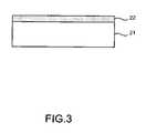
(b) Growing an amorphous Si film12: As shown inFIG. 3 , anamorphous Si film 22 is grown on a surface of thefirst Si substrate 21, where theamorphous Si film 22 is obtained through evaporation, film growth or heat treatment.
(c) Obtaining a second substrate13: As shown inFIG. 4 , asecond Si substrate 23 having abarrier layer 24 and anAu layer 25 is obtained, where thebarrier layer 24 and theAu layer 25 are adhered on thesecond Si substrate 23 with anadhesion layer 27.
(d) Obtaining a bonding structure14: As shown inFIG. 5 , theamorphous Si film 22 on thefirst Si substrate 21 is in contact with theAu layer 25 on thesecond substrate 23 to be processed with a heating and a pressing for obtaining an eutectic reaction area, so that a Si/Aueutectic alloy 26 is obtained through bonding. Thus, a bonding structure with an interface having a fast reaction ratio and a uniformed reaction is obtained.
Please refer toFIG. 6 toFIG. 10 , which are a flow view and structural views showing a second preferred embodiment. As shown in the figures, the present invention is a method for fabricating an amorphous Si/Au eutectic wafer bonding structure, comprising the following steps:
(a) Obtaining a first Si substrate31: As shown inFIG. 7 , afirst Si substrate 41 is obtained.
(b) Growing an amorphous Si film32: As shown inFIG. 8 , abarrier layer 42 and anamorphous Si film 43 are adhered to thefirst substrate 41 through anadhesion layer 47, where theamorphous Si film 43 has a thickness of one micrometer and is obtained through evaporation, film growth or heat treatment.
(c) Obtaining a second substrate33: As shown inFIG. 9 , asecond Si substrate 44 having abarrier layer 42 and anAu layer 45 is obtained, where thebarrier layer 42 and theAu layer 45 are adhered on thesecond Si substrate 44 with anadhesion layer 47.
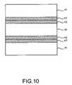
(d) Obtaining a bonding structure34: As shown inFIG. 10 , theamorphous Si film 43 on thefirst Si substrate 41 is in contact with theAu layer 45 on thesecond substrate 44 to be processed with a heating and a pressing for obtaining an eutectic reaction area, so that a Si/Aueutectic alloy 26 is obtained through bonding.
Therein, thebarrier layer 42 prevents the Si/Aueutectic alloy 46 from diffusing out of the eutectic reaction area and prevents exterior objects from diffusing into the eutectic reaction area; and thebarrier layer 42 controls Si provided in the eutectic reaction area to be prevented from being precipitated after the eutectic reaction. And the bonding structure is a structure of barrier-layer/Au/eutectic-alloy/Au/barrier-layer, or barrier-layer/eutectic-alloy/barrier-layer. Thus, a bonding structure with an interface having a fast reaction ratio and a uniformed reaction is obtained.
To sum up, the present invention is a method for fabricating an amorphous Si/Au eutectic wafer bonding structure, where an amorphous Si is obtained through coating or growth to be in contact with Au for bonding to obtain an eutectic wafer bonding structure; Si is prevented from being precipitated; and the bonding structure has an interface having a fast reaction ratio and a uniformed reaction and thus an electrical device having an improved electricity and reliability is obtained.
The preferred embodiments herein disclosed are not intended to unnecessarily limit the scope of the invention. Therefore, simple modifications or variations belonging to the equivalent of the scope of the claims and the instructions disclosed herein for a patent are all within the scope of the present invention.
Claims (9)
1. A method for fabricating an amorphous Si(silicon)/Au(gold) eutectic wafer bonding structure, comprising steps of:
(a) obtaining a first Si substrate;
(b) growing an amorphous Si film on said first Si substrate;
(c) obtaining a second substrate having a barrier layer and an Au layer; and
(d) contacting said amorphous Si film and said Au layer to obtain a bonding structure by processing an eutectic reaction to said amorphous Si film and said Au layer.
2. The method according toclaim 1 ,
wherein said amorphous Si film is obtained by using a method selected from a group consisting of evaporation, film growth and heat treatment.
3. The method according toclaim 1 ,
wherein said amorphous Si film has a thickness of 1 micrometer (μm).
4. A method for fabricating an amorphous Si/Au eutectic wafer bonding structure, comprising steps of:
(a) obtaining a first Si substrate;
(b) obtaining a barrier layer and an amorphous Si film on a surface of said first substrate;
(c) obtaining a second substrate having a barrier layer and an Au layer; and
(d) contacting said amorphous Si film and said Au layer to obtain a bonding structure by processing an eutectic reaction to said amorphous Si film and said Au layer.
5. The method according toclaim 4 ,
wherein said amorphous Si film is obtained by using a method selected from a group consisting of evaporation, film growth and heat treatment.
6. The method according toclaim 4 ,
wherein said amorphous Si film has a thickness of 1 μm.
7. The method according toclaim 4 ,
wherein said barrier layer prevents said Si/Au eutectic alloy from diffusing out of an area of said eutectic reaction; and
wherein said barrier layer prevents exterior objects from diffusing into said area of said eutectic reaction.
8. The method according toclaim 4 ,
wherein said barrier layer prevents Si provided in an area of said eutectic reaction from being precipitated after said eutectic reaction.
9. The method according toclaim 1 ,
wherein said bonding structure is a structure selected from a group consisting of barrier-layer/Au/eutectic-alloy/Au/barrier-layer, and barrier-layer/eutectic-alloy/barrier-layer.
Applications Claiming Priority (2)
| Application Number | Priority Date | Filing Date | Title |
|---|---|---|---|
| TW095145637ATW200826150A (en) | 2006-12-07 | 2006-12-07 | Amorphous silicon-gold covalent structure |
| TW095145637 | 2006-12-07 |
Publications (2)
| Publication Number | Publication Date |
|---|---|
| US20080138965A1 US20080138965A1 (en) | 2008-06-12 |
| US7507636B2true US7507636B2 (en) | 2009-03-24 |
Family
ID=39498584
Family Applications (1)
| Application Number | Title | Priority Date | Filing Date |
|---|---|---|---|
| US11/649,892Expired - Fee RelatedUS7507636B2 (en) | 2006-12-07 | 2007-01-05 | Amorphous Si/Au eutectic wafer bonding structure |
Country Status (2)
| Country | Link |
|---|---|
| US (1) | US7507636B2 (en) |
| TW (1) | TW200826150A (en) |
Families Citing this family (2)
| Publication number | Priority date | Publication date | Assignee | Title |
|---|---|---|---|---|
| EP2392697A1 (en) | 2010-06-03 | 2011-12-07 | The Provost, Fellows and Scholars of the College of the Holy and Undivided Trinity of Queen Elizabeth near Dublin | Method and system for growing nano-scale materials |
| CN103744778A (en)* | 2013-12-29 | 2014-04-23 | 哈尔滨工业大学 | Change point based ISQ-FDEFCE software reliability growth model |
Citations (4)
| Publication number | Priority date | Publication date | Assignee | Title |
|---|---|---|---|---|
| US5668033A (en)* | 1995-05-18 | 1997-09-16 | Nippondenso Co., Ltd. | Method for manufacturing a semiconductor acceleration sensor device |
| US6242324B1 (en)* | 1999-08-10 | 2001-06-05 | The United States Of America As Represented By The Secretary Of The Navy | Method for fabricating singe crystal materials over CMOS devices |
| US6607969B1 (en)* | 2002-03-18 | 2003-08-19 | The United States Of America As Represented By The Secretary Of The Navy | Method for making pyroelectric, electro-optical and decoupling capacitors using thin film transfer and hydrogen ion splitting techniques |
| US20060273810A1 (en)* | 2005-05-24 | 2006-12-07 | Paul Ganitzer | Silicon wafer with solderable coating on its wafer rear side, and process for producing it |
- 2006
- 2006-12-07TWTW095145637Apatent/TW200826150A/ennot_activeIP Right Cessation
- 2007
- 2007-01-05USUS11/649,892patent/US7507636B2/ennot_activeExpired - Fee Related
Patent Citations (4)
| Publication number | Priority date | Publication date | Assignee | Title |
|---|---|---|---|---|
| US5668033A (en)* | 1995-05-18 | 1997-09-16 | Nippondenso Co., Ltd. | Method for manufacturing a semiconductor acceleration sensor device |
| US6242324B1 (en)* | 1999-08-10 | 2001-06-05 | The United States Of America As Represented By The Secretary Of The Navy | Method for fabricating singe crystal materials over CMOS devices |
| US6607969B1 (en)* | 2002-03-18 | 2003-08-19 | The United States Of America As Represented By The Secretary Of The Navy | Method for making pyroelectric, electro-optical and decoupling capacitors using thin film transfer and hydrogen ion splitting techniques |
| US20060273810A1 (en)* | 2005-05-24 | 2006-12-07 | Paul Ganitzer | Silicon wafer with solderable coating on its wafer rear side, and process for producing it |
Also Published As
| Publication number | Publication date |
|---|---|
| TWI319202B (en) | 2010-01-01 |
| US20080138965A1 (en) | 2008-06-12 |
| TW200826150A (en) | 2008-06-16 |
Similar Documents
| Publication | Publication Date | Title |
|---|---|---|
| TWI243488B (en) | Electrical contact-area for optoelectronic semiconductor-chip and its production method | |
| US8330271B2 (en) | Semiconductor element, method for manufacturing the same, and mounting structure having the semiconductor element mounted thereon | |
| US6562648B1 (en) | Structure and method for separation and transfer of semiconductor thin films onto dissimilar substrate materials | |
| TWI283031B (en) | Method for integrating compound semiconductor with substrate of high thermal conductivity | |
| US8598688B2 (en) | Semiconductor device | |
| JP2001185519A5 (en) | ||
| US8381964B2 (en) | Tin-silver bonding and method thereof | |
| EP1873817A3 (en) | Substrate having thin film of GaN joined thereon and method of fabricating the same, and a GaN-based semiconductor device and method of fabricating the same | |
| US11316058B2 (en) | Stacked multi-junction solar cell with a metallization comprising a multilayer system | |
| TW200947602A (en) | Support plate | |
| US7507636B2 (en) | Amorphous Si/Au eutectic wafer bonding structure | |
| EP1928014A3 (en) | Charge trap layer for a charge trap semiconductor memory device and method of manufacturing the same | |
| US8420505B2 (en) | Process for manufacture of thin wafer | |
| US4232440A (en) | Contact structure for light emitting device | |
| US20070231954A1 (en) | Gold/silicon eutectic die bonding method | |
| US8722528B2 (en) | Die backside standoff structures for semiconductor devices | |
| US7391061B2 (en) | Light emitting diode with thermal spreading layer | |
| US7659191B2 (en) | Gold/silicon eutectic die bonding method | |
| US20170040272A1 (en) | Integrated circuits having copper bonding structures with silicon carbon nitride passivation layers thereon and methods for fabricating same | |
| JPWO2015107796A1 (en) | Semiconductor element, manufacturing method thereof, and semiconductor device | |
| US20050040212A1 (en) | Method for manufacturing nitride light-emitting device | |
| JP2009059904A (en) | Sub-mount and semiconductor device equipped with it | |
| JP2006294685A (en) | Semiconductor chip having back metal film and manufacturing method thereof | |
| TWI312564B (en) | Method for manufacturing semiconductor device | |
| JP2004111828A (en) | Transfer mask and exposure method |
Legal Events
| Date | Code | Title | Description |
|---|---|---|---|
| AS | Assignment | Owner name:NATIONAL CENTRAL UNIVERSITY, TAIWAN Free format text:ASSIGNMENT OF ASSIGNORS INTEREST;ASSIGNORS:LIU, CHENG-YI;CHAN, PO-HAN;LIN, CHING-LIANG;REEL/FRAME:018765/0092 Effective date:20061223 | |
| STCF | Information on status: patent grant | Free format text:PATENTED CASE | |
| FPAY | Fee payment | Year of fee payment:4 | |
| FPAY | Fee payment | Year of fee payment:8 | |
| FEPP | Fee payment procedure | Free format text:MAINTENANCE FEE REMINDER MAILED (ORIGINAL EVENT CODE: REM.); ENTITY STATUS OF PATENT OWNER: SMALL ENTITY | |
| LAPS | Lapse for failure to pay maintenance fees | Free format text:PATENT EXPIRED FOR FAILURE TO PAY MAINTENANCE FEES (ORIGINAL EVENT CODE: EXP.); ENTITY STATUS OF PATENT OWNER: SMALL ENTITY | |
| STCH | Information on status: patent discontinuation | Free format text:PATENT EXPIRED DUE TO NONPAYMENT OF MAINTENANCE FEES UNDER 37 CFR 1.362 | |
| FP | Lapsed due to failure to pay maintenance fee | Effective date:20210324 |