US7506438B1 - Low profile integrated module interconnects and method of fabrication - Google Patents
Low profile integrated module interconnects and method of fabricationDownload PDFInfo
- Publication number
- US7506438B1 US7506438B1US09/712,749US71274900AUS7506438B1US 7506438 B1US7506438 B1US 7506438B1US 71274900 AUS71274900 AUS 71274900AUS 7506438 B1US7506438 B1US 7506438B1
- Authority
- US
- United States
- Prior art keywords
- sheets
- integrated module
- providing
- sheet
- fabricating
- Prior art date
- Legal status (The legal status is an assumption and is not a legal conclusion. Google has not performed a legal analysis and makes no representation as to the accuracy of the status listed.)
- Expired - Lifetime, expires
Links
Images


Classifications
- H—ELECTRICITY
- H05—ELECTRIC TECHNIQUES NOT OTHERWISE PROVIDED FOR
- H05K—PRINTED CIRCUITS; CASINGS OR CONSTRUCTIONAL DETAILS OF ELECTRIC APPARATUS; MANUFACTURE OF ASSEMBLAGES OF ELECTRICAL COMPONENTS
- H05K3/00—Apparatus or processes for manufacturing printed circuits
- H05K3/40—Forming printed elements for providing electric connections to or between printed circuits
- H05K3/403—Edge contacts; Windows or holes in the substrate having plural connections on the walls thereof
- H—ELECTRICITY
- H05—ELECTRIC TECHNIQUES NOT OTHERWISE PROVIDED FOR
- H05K—PRINTED CIRCUITS; CASINGS OR CONSTRUCTIONAL DETAILS OF ELECTRIC APPARATUS; MANUFACTURE OF ASSEMBLAGES OF ELECTRICAL COMPONENTS
- H05K1/00—Printed circuits
- H05K1/18—Printed circuits structurally associated with non-printed electric components
- H—ELECTRICITY
- H01—ELECTRIC ELEMENTS
- H01L—SEMICONDUCTOR DEVICES NOT COVERED BY CLASS H10
- H01L21/00—Processes or apparatus adapted for the manufacture or treatment of semiconductor or solid state devices or of parts thereof
- H01L21/02—Manufacture or treatment of semiconductor devices or of parts thereof
- H01L21/04—Manufacture or treatment of semiconductor devices or of parts thereof the devices having potential barriers, e.g. a PN junction, depletion layer or carrier concentration layer
- H01L21/48—Manufacture or treatment of parts, e.g. containers, prior to assembly of the devices, using processes not provided for in a single one of the groups H01L21/18 - H01L21/326 or H10D48/04 - H10D48/07
- H01L21/4814—Conductive parts
- H01L21/4846—Leads on or in insulating or insulated substrates, e.g. metallisation
- H01L21/4857—Multilayer substrates
- H—ELECTRICITY
- H01—ELECTRIC ELEMENTS
- H01L—SEMICONDUCTOR DEVICES NOT COVERED BY CLASS H10
- H01L23/00—Details of semiconductor or other solid state devices
- H01L23/48—Arrangements for conducting electric current to or from the solid state body in operation, e.g. leads, terminal arrangements ; Selection of materials therefor
- H01L23/488—Arrangements for conducting electric current to or from the solid state body in operation, e.g. leads, terminal arrangements ; Selection of materials therefor consisting of soldered or bonded constructions
- H01L23/498—Leads, i.e. metallisations or lead-frames on insulating substrates, e.g. chip carriers
- H01L23/49805—Leads, i.e. metallisations or lead-frames on insulating substrates, e.g. chip carriers the leads being also applied on the sidewalls or the bottom of the substrate, e.g. leadless packages for surface mounting
- H—ELECTRICITY
- H05—ELECTRIC TECHNIQUES NOT OTHERWISE PROVIDED FOR
- H05K—PRINTED CIRCUITS; CASINGS OR CONSTRUCTIONAL DETAILS OF ELECTRIC APPARATUS; MANUFACTURE OF ASSEMBLAGES OF ELECTRICAL COMPONENTS
- H05K3/00—Apparatus or processes for manufacturing printed circuits
- H05K3/30—Assembling printed circuits with electric components, e.g. with resistor
- H05K3/32—Assembling printed circuits with electric components, e.g. with resistor electrically connecting electric components or wires to printed circuits
- H05K3/34—Assembling printed circuits with electric components, e.g. with resistor electrically connecting electric components or wires to printed circuits by soldering
- H05K3/341—Surface mounted components
- H—ELECTRICITY
- H01—ELECTRIC ELEMENTS
- H01L—SEMICONDUCTOR DEVICES NOT COVERED BY CLASS H10
- H01L2224/00—Indexing scheme for arrangements for connecting or disconnecting semiconductor or solid-state bodies and methods related thereto as covered by H01L24/00
- H01L2224/01—Means for bonding being attached to, or being formed on, the surface to be connected, e.g. chip-to-package, die-attach, "first-level" interconnects; Manufacturing methods related thereto
- H01L2224/02—Bonding areas; Manufacturing methods related thereto
- H01L2224/04—Structure, shape, material or disposition of the bonding areas prior to the connecting process
- H01L2224/05—Structure, shape, material or disposition of the bonding areas prior to the connecting process of an individual bonding area
- H01L2224/0554—External layer
- H01L2224/0556—Disposition
- H01L2224/05568—Disposition the whole external layer protruding from the surface
- H—ELECTRICITY
- H01—ELECTRIC ELEMENTS
- H01L—SEMICONDUCTOR DEVICES NOT COVERED BY CLASS H10
- H01L2224/00—Indexing scheme for arrangements for connecting or disconnecting semiconductor or solid-state bodies and methods related thereto as covered by H01L24/00
- H01L2224/01—Means for bonding being attached to, or being formed on, the surface to be connected, e.g. chip-to-package, die-attach, "first-level" interconnects; Manufacturing methods related thereto
- H01L2224/02—Bonding areas; Manufacturing methods related thereto
- H01L2224/04—Structure, shape, material or disposition of the bonding areas prior to the connecting process
- H01L2224/05—Structure, shape, material or disposition of the bonding areas prior to the connecting process of an individual bonding area
- H01L2224/0554—External layer
- H01L2224/05573—Single external layer
- H—ELECTRICITY
- H01—ELECTRIC ELEMENTS
- H01L—SEMICONDUCTOR DEVICES NOT COVERED BY CLASS H10
- H01L2224/00—Indexing scheme for arrangements for connecting or disconnecting semiconductor or solid-state bodies and methods related thereto as covered by H01L24/00
- H01L2224/01—Means for bonding being attached to, or being formed on, the surface to be connected, e.g. chip-to-package, die-attach, "first-level" interconnects; Manufacturing methods related thereto
- H01L2224/10—Bump connectors; Manufacturing methods related thereto
- H01L2224/15—Structure, shape, material or disposition of the bump connectors after the connecting process
- H01L2224/16—Structure, shape, material or disposition of the bump connectors after the connecting process of an individual bump connector
- H01L2224/161—Disposition
- H01L2224/16151—Disposition the bump connector connecting between a semiconductor or solid-state body and an item not being a semiconductor or solid-state body, e.g. chip-to-substrate, chip-to-passive
- H01L2224/16221—Disposition the bump connector connecting between a semiconductor or solid-state body and an item not being a semiconductor or solid-state body, e.g. chip-to-substrate, chip-to-passive the body and the item being stacked
- H01L2224/16225—Disposition the bump connector connecting between a semiconductor or solid-state body and an item not being a semiconductor or solid-state body, e.g. chip-to-substrate, chip-to-passive the body and the item being stacked the item being non-metallic, e.g. insulating substrate with or without metallisation
- H—ELECTRICITY
- H01—ELECTRIC ELEMENTS
- H01L—SEMICONDUCTOR DEVICES NOT COVERED BY CLASS H10
- H01L2924/00—Indexing scheme for arrangements or methods for connecting or disconnecting semiconductor or solid-state bodies as covered by H01L24/00
- H01L2924/0001—Technical content checked by a classifier
- H01L2924/00014—Technical content checked by a classifier the subject-matter covered by the group, the symbol of which is combined with the symbol of this group, being disclosed without further technical details
- H—ELECTRICITY
- H05—ELECTRIC TECHNIQUES NOT OTHERWISE PROVIDED FOR
- H05K—PRINTED CIRCUITS; CASINGS OR CONSTRUCTIONAL DETAILS OF ELECTRIC APPARATUS; MANUFACTURE OF ASSEMBLAGES OF ELECTRICAL COMPONENTS
- H05K1/00—Printed circuits
- H05K1/02—Details
- H05K1/03—Use of materials for the substrate
- H05K1/0306—Inorganic insulating substrates, e.g. ceramic, glass
- H—ELECTRICITY
- H05—ELECTRIC TECHNIQUES NOT OTHERWISE PROVIDED FOR
- H05K—PRINTED CIRCUITS; CASINGS OR CONSTRUCTIONAL DETAILS OF ELECTRIC APPARATUS; MANUFACTURE OF ASSEMBLAGES OF ELECTRICAL COMPONENTS
- H05K2201/00—Indexing scheme relating to printed circuits covered by H05K1/00
- H05K2201/09—Shape and layout
- H05K2201/09145—Edge details
- H05K2201/09181—Notches in edge pads
- H—ELECTRICITY
- H05—ELECTRIC TECHNIQUES NOT OTHERWISE PROVIDED FOR
- H05K—PRINTED CIRCUITS; CASINGS OR CONSTRUCTIONAL DETAILS OF ELECTRIC APPARATUS; MANUFACTURE OF ASSEMBLAGES OF ELECTRICAL COMPONENTS
- H05K2201/00—Indexing scheme relating to printed circuits covered by H05K1/00
- H05K2201/09—Shape and layout
- H05K2201/09209—Shape and layout details of conductors
- H05K2201/09654—Shape and layout details of conductors covering at least two types of conductors provided for in H05K2201/09218 - H05K2201/095
- H05K2201/09781—Dummy conductors, i.e. not used for normal transport of current; Dummy electrodes of components
- H—ELECTRICITY
- H05—ELECTRIC TECHNIQUES NOT OTHERWISE PROVIDED FOR
- H05K—PRINTED CIRCUITS; CASINGS OR CONSTRUCTIONAL DETAILS OF ELECTRIC APPARATUS; MANUFACTURE OF ASSEMBLAGES OF ELECTRICAL COMPONENTS
- H05K2201/00—Indexing scheme relating to printed circuits covered by H05K1/00
- H05K2201/10—Details of components or other objects attached to or integrated in a printed circuit board
- H05K2201/10613—Details of electrical connections of non-printed components, e.g. special leads
- H05K2201/10954—Other details of electrical connections
- H05K2201/10969—Metallic case or integral heatsink of component electrically connected to a pad on PCB
- H—ELECTRICITY
- H05—ELECTRIC TECHNIQUES NOT OTHERWISE PROVIDED FOR
- H05K—PRINTED CIRCUITS; CASINGS OR CONSTRUCTIONAL DETAILS OF ELECTRIC APPARATUS; MANUFACTURE OF ASSEMBLAGES OF ELECTRICAL COMPONENTS
- H05K3/00—Apparatus or processes for manufacturing printed circuits
- H05K3/0011—Working of insulating substrates or insulating layers
- H05K3/0044—Mechanical working of the substrate, e.g. drilling or punching
- H05K3/0052—Depaneling, i.e. dividing a panel into circuit boards; Working of the edges of circuit boards
- H—ELECTRICITY
- H05—ELECTRIC TECHNIQUES NOT OTHERWISE PROVIDED FOR
- H05K—PRINTED CIRCUITS; CASINGS OR CONSTRUCTIONAL DETAILS OF ELECTRIC APPARATUS; MANUFACTURE OF ASSEMBLAGES OF ELECTRICAL COMPONENTS
- H05K3/00—Apparatus or processes for manufacturing printed circuits
- H05K3/30—Assembling printed circuits with electric components, e.g. with resistor
- H05K3/32—Assembling printed circuits with electric components, e.g. with resistor electrically connecting electric components or wires to printed circuits
- H05K3/34—Assembling printed circuits with electric components, e.g. with resistor electrically connecting electric components or wires to printed circuits by soldering
- H05K3/341—Surface mounted components
- H05K3/3431—Leadless components
- H05K3/3442—Leadless components having edge contacts, e.g. leadless chip capacitors, chip carriers
- H—ELECTRICITY
- H05—ELECTRIC TECHNIQUES NOT OTHERWISE PROVIDED FOR
- H05K—PRINTED CIRCUITS; CASINGS OR CONSTRUCTIONAL DETAILS OF ELECTRIC APPARATUS; MANUFACTURE OF ASSEMBLAGES OF ELECTRICAL COMPONENTS
- H05K3/00—Apparatus or processes for manufacturing printed circuits
- H05K3/30—Assembling printed circuits with electric components, e.g. with resistor
- H05K3/32—Assembling printed circuits with electric components, e.g. with resistor electrically connecting electric components or wires to printed circuits
- H05K3/34—Assembling printed circuits with electric components, e.g. with resistor electrically connecting electric components or wires to printed circuits by soldering
- H05K3/3457—Solder materials or compositions; Methods of application thereof
- H05K3/3485—Applying solder paste, slurry or powder
- H—ELECTRICITY
- H05—ELECTRIC TECHNIQUES NOT OTHERWISE PROVIDED FOR
- H05K—PRINTED CIRCUITS; CASINGS OR CONSTRUCTIONAL DETAILS OF ELECTRIC APPARATUS; MANUFACTURE OF ASSEMBLAGES OF ELECTRICAL COMPONENTS
- H05K3/00—Apparatus or processes for manufacturing printed circuits
- H05K3/40—Forming printed elements for providing electric connections to or between printed circuits
- H05K3/4038—Through-connections; Vertical interconnect access [VIA] connections
- H05K3/4053—Through-connections; Vertical interconnect access [VIA] connections by thick-film techniques
- H05K3/4061—Through-connections; Vertical interconnect access [VIA] connections by thick-film techniques for via connections in inorganic insulating substrates
- Y—GENERAL TAGGING OF NEW TECHNOLOGICAL DEVELOPMENTS; GENERAL TAGGING OF CROSS-SECTIONAL TECHNOLOGIES SPANNING OVER SEVERAL SECTIONS OF THE IPC; TECHNICAL SUBJECTS COVERED BY FORMER USPC CROSS-REFERENCE ART COLLECTIONS [XRACs] AND DIGESTS
- Y02—TECHNOLOGIES OR APPLICATIONS FOR MITIGATION OR ADAPTATION AGAINST CLIMATE CHANGE
- Y02P—CLIMATE CHANGE MITIGATION TECHNOLOGIES IN THE PRODUCTION OR PROCESSING OF GOODS
- Y02P70/00—Climate change mitigation technologies in the production process for final industrial or consumer products
- Y02P70/50—Manufacturing or production processes characterised by the final manufactured product
- Y—GENERAL TAGGING OF NEW TECHNOLOGICAL DEVELOPMENTS; GENERAL TAGGING OF CROSS-SECTIONAL TECHNOLOGIES SPANNING OVER SEVERAL SECTIONS OF THE IPC; TECHNICAL SUBJECTS COVERED BY FORMER USPC CROSS-REFERENCE ART COLLECTIONS [XRACs] AND DIGESTS
- Y10—TECHNICAL SUBJECTS COVERED BY FORMER USPC
- Y10T—TECHNICAL SUBJECTS COVERED BY FORMER US CLASSIFICATION
- Y10T29/00—Metal working
- Y10T29/49—Method of mechanical manufacture
- Y10T29/49002—Electrical device making
- Y10T29/49117—Conductor or circuit manufacturing
- Y10T29/49124—On flat or curved insulated base, e.g., printed circuit, etc.
- Y10T29/4913—Assembling to base an electrical component, e.g., capacitor, etc.
- Y—GENERAL TAGGING OF NEW TECHNOLOGICAL DEVELOPMENTS; GENERAL TAGGING OF CROSS-SECTIONAL TECHNOLOGIES SPANNING OVER SEVERAL SECTIONS OF THE IPC; TECHNICAL SUBJECTS COVERED BY FORMER USPC CROSS-REFERENCE ART COLLECTIONS [XRACs] AND DIGESTS
- Y10—TECHNICAL SUBJECTS COVERED BY FORMER USPC
- Y10T—TECHNICAL SUBJECTS COVERED BY FORMER US CLASSIFICATION
- Y10T29/00—Metal working
- Y10T29/49—Method of mechanical manufacture
- Y10T29/49002—Electrical device making
- Y10T29/49117—Conductor or circuit manufacturing
- Y10T29/49124—On flat or curved insulated base, e.g., printed circuit, etc.
- Y10T29/49155—Manufacturing circuit on or in base
- Y10T29/49165—Manufacturing circuit on or in base by forming conductive walled aperture in base
Definitions
- This inventionrelates to apparatus and method for interconnecting integrated modules.
- the present inventionrelates to apparatus and method for interconnecting integrated modules with low profile interconnects having improved reliability.
- the integrated moduleshave electrical traces distributed around the lower surface.
- the electrical traces of the integrated modulesare electrically and physically connected to mounting and connecting pads on a printed circuit board by means of solder balls.
- the center of the module's lower surfacecan be considered as a zero stress or neutral point with connections spaced from the center having more stress, and the farther connections are spaced from the center the more stress they realize.
- Some of this stressis relieved by the solder balls, which provide a small amount of resiliency or movement.
- the height of the solder ballis increased.
- the standoff height and the distance of the solder joint from the thermal expansion neutral pointare well known to be the most critical factors responsible for solder joint thermal fatigue. Higher standoff heights and smaller distances from the thermal expansion neutral point are preferable.
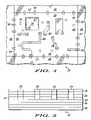
- FIG. 1is a simplified side view of a prior art module, illustrating the mounting structure
- FIG. 2is a simplified view in bottom plan of a prior art module, illustrating thermal expansion distances from the thermal expansion neutral point;
- FIG. 3is an enlarged sectional view of a portion of an assembly including a plurality of modules in accordance with the present invention
- FIG. 4is a greatly enlarged, detailed view of a portion of a single layer of the assembly of FIG. 3 ;
- FIG. 5is a simplified side view of a single module after being cut from adjacent modules in the assembly of FIG. 3 ;
- FIG. 6is a simplified view in bottom plan of the module of FIG. 5 ;
- FIG. 7is a view in bottom plan, similar to FIG. 6 , of a module including a stress relief anchor pad;
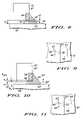
- FIG. 8is an enlarged sectional view of a single solder connection to a module in accordance with the present invention, taken along line 8 - 8 of FIG. 7 ;
- FIG. 9is a top view of a portion of the module in accordance with FIG. 8 ;
- FIG. 10is an enlarged sectional view of another single solder connection to a module in accordance with the present invention.
- FIG. 11is a top view of a portion of the module in accordance with FIG. 10 .
- Module 10includes a plurality of terminals 11 formed on the lower surface thereof. As is well known in the art, terminals 11 are connected internally to the circuits and components integrated within module 10 . Terminals 11 also serve to mount module 10 on a supporting substrate 12 . Supporting substrate 12 has a plurality of mounting/connecting pads 14 formed on the upper or mounting surface 15 and positioned to coincide with terminals 11 of module 10 . Solder balls 16 are positioned between terminals 11 and mounting/connecting pads 14 . During assembly, solder balls 16 are partially melted so as to physically and electrically adhere to terminals 11 and mounting/connecting pads 14 . Thus, solder balls 16 physically mount module 10 on supporting substrate 12 and electrically connect terminals 11 to mounting/connecting pads 14 .
- a central point, designated 17 , of the lower surface of module 10is considered as a zero stress or neutral point with terminals 11 spaced from point 17 having increasing amounts of stress. The farther terminals 11 are spaced from point 17 the more stress they realize.
- a terminal 11 situated in the corner of module 10is spaced the farthest from point 17 and experiences the most stress, indicated by an arrow 18 .
- Some of this stressis relieved by solder balls 16 (see FIG. 1 ), which provide a small amount of resiliency or movement.
- the standoff height(designated h s in FIG. 1 ) between the lower surface of module 10 and upper surface 15 of supporting substrate 12 is increased.
- the standoff height h s and the distance of the solder joint from thermal expansion neutral point 17are well known to be the most critical factors responsible for SMT solder joint thermal fatigue.
- assembly 20is illustrated to aid in describing a method of fabricating a low profile integrated module, in accordance with the present invention.
- assembly 20could include a wide variety of sheets of materials, such as ceramic materials, high density interconnect printed circuit boards (HDI/PCB), presently known as FR4, and substantially any material wherein electrical circuits and components are included in sheets and stacked to form a complete circuit or electrical component.
- HDI/PCBhigh density interconnect printed circuit boards
- a plurality of sheets 25 of unfired or green ceramic materialare provided for exemplary purposes.
- a typical example of one sheet 25is illustrated in FIG. 4 .
- Each sheet 25includes a plurality of module components 26 defined by sides 27 and formed adjacent each other so as to share sides 27 .
- Each component 26includes some electrical traces (designated 28 in FIG. 4 ), and may further include some electrical components such as capacitors, inductors, resistors, semiconductor integrated circuits (such as an IC designated 29 ), etc.
- Each component 26also includes vias extending therethrough, some of which (designated 30 ) are located intermediately between sides 27 and some of which (designated 32 ) are formed in an elongated configuration to extend across sides 27 into adjacent components 26 .
- vias 30are formed, using punches, drills, lasers, etc. (hereinafter referred to as “punching”).
- Vias 32are formed by punching a plurality of adjacent, partially overlapping, substantially round holes (referred to hereinafter as nibbling) to define a single via with an elongated cross-section.
- nibblinga plurality of adjacent, partially overlapping, substantially round holes
- FIGS. 4 and 6are illustrated only to simplify an understanding of the fabrication process.
- the cross-sectional dimension of the exposed face of via 32designated 33 in FIG. 6 , is in a range of 125 ⁇ m to 500 ⁇ m.
- sheets 25are formed of unfired or green ceramic material which, as is known in the art, usually includes Al 2 O 3 particles, glass particles, and a binder, generally including organic material.
- a metal pastein this preferred embodiment an 80% silver and a solvent, is forced into the vias as, for example, by using a squeegee or the like.
- the solvent in the silver pastehas a tendency to creep into the unfired ceramic material sides of the vias and firmly bind the silver paste in the vias.
- the metal pastecan include any electrically conductive metal with a melting point generally greater than the firing temperature of the green ceramic sheets, i.e., generally greater than 800° C. It will further be understood that normal solders and the like can be used, if desired, in sheets of material which do not require high temperature curing or firing, such as the FR4 mentioned above.
- a plurality of sheets 25are stacked or positioned in overlying relationship with sides 27 and vias 32 vertically aligned to form common vias 32 and common sides 27 through the entire stack. It will of course be understood that internal vias 30 and various other connections are also aligned to provide one or more complete interconnected circuits.
- Another plurality of sheets 35are fabricated to include module components similar to module components 26 of sheets 25 .
- the fabrication process for sheets 35is similar to that described above for sheets 25 , except that vias 32 are not included.
- Sheets 35include some electrical traces, and may also include some electrical components such as capacitors, inductors, resistors, semiconductor integrated circuits, etc.
- Sheets 35include intermediate vias, similar to vias 30 in sheets 25 , to provide interconnects between the various sheets 35 and 25 .
- the plurality of sheets 35(in this example three) are stacked or positioned in overlying relationship with the sides and any vias and components aligned to form one or more complete interconnected circuits.
- sheets 25are stacked in overlying relationship over sheets 35 with sides 27 aligned so as to form a plurality of vertically aligned modules 21 , 22 , and 23 .
- Modules 21 , 22 , and 23are positioned in adjacent abutting relationship so as to share common sides 27 with the next adjacent module on each side.
- sheets 25 and 35are very thin and, generally, the total number of sheets used depends upon the circuit or circuits being integrated as well as any limitations on the height h specified by a user of the module (e.g., 2 mm). Further, the number of sheets 25 and the number of sheets 35 incorporated, depends upon a desired vertical length for the common vias 32 .
- the number of sheets included in stack 20could vary from a minimum of one sheet 25 and one sheet 35 to as many as twenty total sheets, or more.
- the number of sheets 25 and the number of sheets 35 in stack 20is determined so that the common vias 32 extend vertically in a range from approximately 25 ⁇ m to approximately one half of the height of the stack (i.e., a distance between a lower surface of a lower sheet and an upper surface of an upper sheet).
- stack 20 of unfired or green ceramic sheetshas been assembled as illustrated in FIG. 3 , the stack is cut or otherwise divided into individual modules.
- stack 20is cut with a very sharp instrument. The cutting is easily accomplished since sheets 25 and 35 are still formed of unfired or green ceramic.
- Stack 20could be divided into individual modules after firing but fired ceramic is very hard and the process would be substantially more difficult.
- the sides 27 of adjacent modules 21 and 23 and adjacent modules 21 and 22are indicated with broken lines.
- sides 27extend through vias 32 so that upon cutting stack 20 along the broken lines each module 21 , 22 , and 23 has portions of vias 32 extending along the sides thereof, as illustrated in FIG. 6 .
- the cutting processis performed with sheets 25 at the top of the stack and sheets 35 at the bottom of the stack so that silver paste in vias 32 is held in place by the solid surface of sheets 35 during the cutting operation.
- the modulesare fired to cure the ceramic.
- the firing temperatureis generally dictated by the composition of the green ceramic material.
- the green ceramic materialincludes Al 2 O 3 particles, glass particles and an organic binder.
- the glass particlesdictate the firing temperature, since the glass particles melt sufficiently to bind the aluminum particles together at a temperature of approximately 875° C.
- the organic binderis driven off to leave a ceramic comprising Al 2 O 3 particles bound together by at the least partially melted and reformed glass.
- the various sheets 25 and 35are bound into a virtually single structure by the firing process. In the firing process the individual modules contract or shrink approximately 13%, but the shrinkage is substantially uniform so that it does not affect the final module. Further, during the firing process the silver paste in vias 30 and 32 is hardened firmly into position.
- FIG. 7a bottom view of another final module 21 is illustrated.
- a plurality of vias 32are distributed along each side 27 and a stress relief anchor pad is positioned on the bottom surface.
- the stress relief padincludes a centrally located octagonal element 36 and a round element 37 positioned in each corner.
- the stress relief padis formed on the lower surface of the final sheet 25 (e.g., the top sheet in FIG. 3 ) and includes metal that is ultimately soldered to a supporting substrate (as will be described presently).
- a central point of the lower surface of a moduleis considered as a zero stress or neutral point and the farther terminals are spaced from the neutral point the more stress they realize.
- the stress relief padreduces stresses at adjacent interconnects or vias 32 .
- Octagonal element 36 and round elements 37are designed and positioned so that each via 32 is spaced approximately an equal and short distance therefrom. It will be understood that octagonal element 36 and round elements 37 could be formed as a single integrated stress relief pad if desired or they could be divided into additional elements, with the purpose being to provide equal and short distances between each via and the stress relief pad.
- the individual fired modulescan then be mounted on a supporting substrate 40 , as illustrated in FIG. 8 .
- supporting substrate 40is a printed circuit board or the like with a mounting surface 42 .
- Mounting pads 43are fabricated on surface 42 using any well known process and a layer of reflowable solder or solder paste is applied using any well known technique, such as printing or the like. While only one mounting pad 43 is illustrated in FIG. 8 , for convenience, it will be understood that any or all of vias 32 , any vias 30 , and/or any stress relief pad or pads, which it is desired to connect to supporting substrate 40 , will generally have an aligned mounting pad 43 associated therewith.
- mounting pads 43are formed with a surface area that is larger than the lower adjoining surface area of the associated via 32 .
- the surface area of mounting pad 43may be generally rectangular with a length to width ratio of about 2:1.
- Soldere.g., solder paste, etc.
- the structureis then heated in a well known fashion to melt or reflow the solder paste or solder positioned on mounting pad 43 .
- the prepositioned solderwicks-up the outside of via 32 to form a fillet 45 , as illustrated in FIG. 8 .
- the amount of prepositioned solderis selected so that the final standoff height a h s is preferably in a range of from 75 ⁇ m to 125 ⁇ m. This range allows the solder associated with the module to be printed at the same time as solder for other board elements or modules and the entire substrate 40 can be printed in one step.
- connection and/or mounting pad 46is provided on the lower surface of the lower sheet 25 of module 21 in contact with the lower surface of each via 32 .
- Pad 46has a surface area larger than the cross-sectional area of via 32 (see FIG. 8 ) so as to spread the stress over a larger area.
- the surface area of mounting pad 43 on supporting substrate 40is then formed with a generally rectangular shape having a length to width ratio of about 2:1 and a surface area at least twice as large as the surface area of pad 46 (see FIG. 9 ).
- FIGS. 10 and 11another embodiment of apparatus for reducing stress is illustrated.
- components similar to those illustrated in FIGS. 8 and 9are designated with similar numbers and a prime is added to each number to indicate the different embodiment.
- a connection and/or mounting pad 46 ′is provided on the lower surface of an interior sheet next to the lower sheet, with one or more lower sheets 25 ′ having cutouts aligned with pad 46 ′. While only one mounting pad 43 ′ is illustrated in FIGS.
- any or all of vias 32 ′, any vias 30 ′, and/or any stress relief pad or pads, which it is desired to connect to supporting substrate 40 ′,will generally have an aligned mounting pad 43 ′ associated therewith.
- pad 46 ′is recessed into the lower surface of module 21 ′ so that the total height of the solder, designated h sol in FIG. 10 , is greater and, therefore, further reduces the stress on the joint.
- pad 46 ′can be recessed one to several sheets of module 21 ′ to increase the height h sol . It should also be noted that by recessing pad 46 ′, the standoff height h s ′ of module 21 ′ can be reduced to 25 ⁇ m or less if it is desired.
- pad 46 ′can be formed of silver in a fashion similar to that described for the filling of the vias.
- the cutout or cutouts in the lower sheet or sheets 25 ′ of module 21 ′can be filled with silver in a fashion similar to that described for the filling of the vias. This cutout enables a thickness increase from 47 to 47 ′ which will provide the additional silver to ensure strong interconnections.
- vias 32 positioned in sides 27 of module 21are constructed to extend only partially up the sides so as to improve the fabrication process.
- the internal circuitrycan be easily connected through internal electrical traces 28 and vias 30 .
- the assembled or stacked unfired ceramic sheets of integrated circuitryare separated or cut while in the green state to greatly simplify the separation process.
- sheets 35form a base for the silver or conductive metal in vias 32 so that they can be easily bisected without driving the silver or conductive metal out.
- the fired and otherwise completed integrated modulesare mounted on a supporting substrate with a greatly reduced standoff height h s ′ (e.g., 75 ⁇ m to 125 ⁇ m versus a 375 ⁇ m ball in the prior art). Because of the conductive metal filled vias positioned along the edge and the size of the mounting pads on the supporting substrate, the solder used in the mounting and connecting process wicks-up the side of the module to form a fillet, which greatly strengthens the connection/mount and substantially increases reliability and life of the solder joint.
- h s ′e.g. 75 ⁇ m to 125 ⁇ m versus a 375 ⁇ m ball in the prior art.
Landscapes
- Engineering & Computer Science (AREA)
- Microelectronics & Electronic Packaging (AREA)
- Manufacturing & Machinery (AREA)
- Power Engineering (AREA)
- Computer Hardware Design (AREA)
- General Physics & Mathematics (AREA)
- Physics & Mathematics (AREA)
- Condensed Matter Physics & Semiconductors (AREA)
- Ceramic Engineering (AREA)
- Structures For Mounting Electric Components On Printed Circuit Boards (AREA)
- Combinations Of Printed Boards (AREA)
- Production Of Multi-Layered Print Wiring Board (AREA)
- Electric Connection Of Electric Components To Printed Circuits (AREA)
Abstract
Description
Claims (22)
Priority Applications (7)
| Application Number | Priority Date | Filing Date | Title |
|---|---|---|---|
| US09/712,749US7506438B1 (en) | 2000-11-14 | 2000-11-14 | Low profile integrated module interconnects and method of fabrication |
| KR1020037006575AKR100895964B1 (en) | 2000-11-14 | 2001-11-07 | Low profile integrated module interconnects |
| AU2002228817AAU2002228817A1 (en) | 2000-11-14 | 2001-11-07 | Low profile integrated module interconnects |
| JP2002543699AJP2004536442A (en) | 2000-11-14 | 2001-11-07 | Low profile integrated module interconnect |
| PCT/US2001/046626WO2002041397A2 (en) | 2000-11-14 | 2001-11-07 | Low profile integrated module interconnects |
| CNB018196993ACN100423252C (en) | 2000-11-14 | 2001-11-07 | Low Profile Integrated Module Interconnect |
| TW090128113ATWI247568B (en) | 2000-11-14 | 2001-11-13 | Low profile integrated module interconnects and method of fabrication |
Applications Claiming Priority (1)
| Application Number | Priority Date | Filing Date | Title |
|---|---|---|---|
| US09/712,749US7506438B1 (en) | 2000-11-14 | 2000-11-14 | Low profile integrated module interconnects and method of fabrication |
Publications (1)
| Publication Number | Publication Date |
|---|---|
| US7506438B1true US7506438B1 (en) | 2009-03-24 |
Family
ID=24863406
Family Applications (1)
| Application Number | Title | Priority Date | Filing Date |
|---|---|---|---|
| US09/712,749Expired - LifetimeUS7506438B1 (en) | 2000-11-14 | 2000-11-14 | Low profile integrated module interconnects and method of fabrication |
Country Status (7)
| Country | Link |
|---|---|
| US (1) | US7506438B1 (en) |
| JP (1) | JP2004536442A (en) |
| KR (1) | KR100895964B1 (en) |
| CN (1) | CN100423252C (en) |
| AU (1) | AU2002228817A1 (en) |
| TW (1) | TWI247568B (en) |
| WO (1) | WO2002041397A2 (en) |
Cited By (9)
| Publication number | Priority date | Publication date | Assignee | Title |
|---|---|---|---|---|
| US20080265428A1 (en)* | 2007-04-26 | 2008-10-30 | International Business Machines Corporation | Via and solder ball shapes to maximize chip or silicon carrier strength relative to thermal or bending load zero point |
| US20110124156A1 (en)* | 2007-05-04 | 2011-05-26 | Stats Chippac, Ltd. | Method of Fabricating Semiconductor Die with Through-Hole Via on Saw Streets and Through-Hole Via in Active Area of Die |
| USD668659S1 (en)* | 2011-11-15 | 2012-10-09 | Connectblue Ab | Module |
| USD668658S1 (en)* | 2011-11-15 | 2012-10-09 | Connectblue Ab | Module |
| USD680119S1 (en)* | 2011-11-15 | 2013-04-16 | Connectblue Ab | Module |
| USD680545S1 (en)* | 2011-11-15 | 2013-04-23 | Connectblue Ab | Module |
| USD689053S1 (en)* | 2011-11-15 | 2013-09-03 | Connectblue Ab | Module |
| USD692896S1 (en)* | 2011-11-15 | 2013-11-05 | Connectblue Ab | Module |
| US20190029115A1 (en)* | 2017-07-19 | 2019-01-24 | Koito Manufacturing Co., Ltd. | On-vehicle electronic circuit mounting board |
Families Citing this family (5)
| Publication number | Priority date | Publication date | Assignee | Title |
|---|---|---|---|---|
| KR20020091785A (en)* | 2001-05-31 | 2002-12-06 | 니혼도꾸슈도교 가부시키가이샤 | Electronic parts and mobile communication device using the same |
| JP3956965B2 (en)* | 2004-09-07 | 2007-08-08 | 日立エーアイシー株式会社 | Chip component type light emitting device and wiring board therefor |
| KR100797696B1 (en)* | 2006-03-14 | 2008-01-23 | 삼성전기주식회사 | Matching method of printed circuit board |
| CN109195354A (en)* | 2018-09-26 | 2019-01-11 | 上海安费诺永亿通讯电子有限公司 | SMT welding structure and welding method in electronic product between two parts |
| CN115988747A (en)* | 2022-12-30 | 2023-04-18 | 上海拿森汽车电子有限公司 | A kind of manufacturing method of compatible PCB board contact and PCB board |
Citations (20)
| Publication number | Priority date | Publication date | Assignee | Title |
|---|---|---|---|---|
| US3606677A (en)* | 1967-12-26 | 1971-09-21 | Rca Corp | Multilayer circuit board techniques |
| US4635093A (en) | 1985-06-03 | 1987-01-06 | General Electric Company | Electrical connection |
| JPS63233598A (en) | 1987-03-23 | 1988-09-29 | 日立エーアイシー株式会社 | Printed wiring board and manufacture of the same |
| US4790894A (en) | 1987-02-19 | 1988-12-13 | Hitachi Condenser Co., Ltd. | Process for producing printed wiring board |
| US5235496A (en) | 1991-04-18 | 1993-08-10 | Texas Instruments Incorporated | Device for packaging integrated circuits |
| EP0582881A1 (en) | 1992-07-27 | 1994-02-16 | Murata Manufacturing Co., Ltd. | Multilayer electronic component, method of manufacturing the same and method of measuring characteristics thereof |
| JPH0696992A (en) | 1992-07-27 | 1994-04-08 | Murata Mfg Co Ltd | Multilayer electronic component, production method thereof, and characteristics measuring method therefor |
| US5547530A (en)* | 1993-02-02 | 1996-08-20 | Matsushita Electric Industrial Co., Ltd. | Method of manufacturing a ceramic substrate |
| US5600101A (en)* | 1994-07-21 | 1997-02-04 | Murata Manufacturing Co., Ltd. | Multilayer electronic component and method of manufacturing the same |
| JPH10163591A (en) | 1996-11-29 | 1998-06-19 | Toshiba Corp | Printed circuit board |
| US5787578A (en)* | 1996-07-09 | 1998-08-04 | International Business Machines Corporation | Method of selectively depositing a metallic layer on a ceramic substrate |
| US5811799A (en) | 1997-07-31 | 1998-09-22 | Wu; Liang-Chung | Image sensor package having a wall with a sealed cover |
| EP0933816A2 (en) | 1998-01-30 | 1999-08-04 | Taiyo Yuden Co., Ltd. | Hybrid module and methods for manufacturing and mounting thereof |
| WO1999041957A1 (en) | 1998-02-13 | 1999-08-19 | Merrimac Industries, Inc. | Method of making microwave, multifunction modules using fluoropolymer composite substrates |
| WO2000019532A1 (en) | 1998-09-30 | 2000-04-06 | Conexant Systems, Inc. | Package for providing improved electrical contact and methods for forming the same |
| EP0997941A2 (en) | 1998-10-28 | 2000-05-03 | Ngk Spark Plug Co., Ltd. | Conductive paste and ceramic printed circuit substrate using the same |
| TW389968B (en) | 1997-07-17 | 2000-05-11 | Wu Liang Jung | Image sensor package |
| EP1050906A1 (en) | 1999-05-06 | 2000-11-08 | Murata Manufacturing Co., Ltd. | Package for electronic components |
| US6249962B1 (en)* | 1997-09-17 | 2001-06-26 | Telefonaktiebolaget Lm Ericsson (Publ) | Process for manufacturing a multi-layer circuit board with supporting layers of different materials |
| US6350334B1 (en)* | 1998-11-02 | 2002-02-26 | Matsushita Electric Industrial Co., Ltd. | Method of manufacturing a multi-layered ceramic substrate |
Family Cites Families (4)
| Publication number | Priority date | Publication date | Assignee | Title |
|---|---|---|---|---|
| IT1145458B (en)* | 1981-02-18 | 1986-11-05 | Omac Srl | AIR VENTILATION OR WATER CIRCULATION DEVICE ISERIBLE IN FIREPLACES |
| NZ204003A (en)* | 1982-04-27 | 1986-05-09 | Wellcome Found | Substituted xanthenes and xanthones and pharmaceutical compositions |
| US5140745A (en)* | 1990-07-23 | 1992-08-25 | Mckenzie Jr Joseph A | Method for forming traces on side edges of printed circuit boards and devices formed thereby |
| GB2283863A (en)* | 1993-11-16 | 1995-05-17 | Ibm | Direct chip attach module |
- 2000
- 2000-11-14USUS09/712,749patent/US7506438B1/ennot_activeExpired - Lifetime
- 2001
- 2001-11-07JPJP2002543699Apatent/JP2004536442A/enactivePending
- 2001-11-07CNCNB018196993Apatent/CN100423252C/ennot_activeExpired - Fee Related
- 2001-11-07KRKR1020037006575Apatent/KR100895964B1/ennot_activeExpired - Fee Related
- 2001-11-07AUAU2002228817Apatent/AU2002228817A1/ennot_activeAbandoned
- 2001-11-07WOPCT/US2001/046626patent/WO2002041397A2/enactiveApplication Filing
- 2001-11-13TWTW090128113Apatent/TWI247568B/ennot_activeIP Right Cessation
Patent Citations (21)
| Publication number | Priority date | Publication date | Assignee | Title |
|---|---|---|---|---|
| US3606677A (en)* | 1967-12-26 | 1971-09-21 | Rca Corp | Multilayer circuit board techniques |
| US4635093A (en) | 1985-06-03 | 1987-01-06 | General Electric Company | Electrical connection |
| US4790894A (en) | 1987-02-19 | 1988-12-13 | Hitachi Condenser Co., Ltd. | Process for producing printed wiring board |
| JPS63233598A (en) | 1987-03-23 | 1988-09-29 | 日立エーアイシー株式会社 | Printed wiring board and manufacture of the same |
| US5235496A (en) | 1991-04-18 | 1993-08-10 | Texas Instruments Incorporated | Device for packaging integrated circuits |
| EP0582881A1 (en) | 1992-07-27 | 1994-02-16 | Murata Manufacturing Co., Ltd. | Multilayer electronic component, method of manufacturing the same and method of measuring characteristics thereof |
| JPH0696992A (en) | 1992-07-27 | 1994-04-08 | Murata Mfg Co Ltd | Multilayer electronic component, production method thereof, and characteristics measuring method therefor |
| US5644107A (en)* | 1992-07-27 | 1997-07-01 | Murata Manufacturing Co., Ltd. | Method of manufacturing a multilayer electronic component |
| US5547530A (en)* | 1993-02-02 | 1996-08-20 | Matsushita Electric Industrial Co., Ltd. | Method of manufacturing a ceramic substrate |
| US5600101A (en)* | 1994-07-21 | 1997-02-04 | Murata Manufacturing Co., Ltd. | Multilayer electronic component and method of manufacturing the same |
| US5787578A (en)* | 1996-07-09 | 1998-08-04 | International Business Machines Corporation | Method of selectively depositing a metallic layer on a ceramic substrate |
| JPH10163591A (en) | 1996-11-29 | 1998-06-19 | Toshiba Corp | Printed circuit board |
| TW389968B (en) | 1997-07-17 | 2000-05-11 | Wu Liang Jung | Image sensor package |
| US5811799A (en) | 1997-07-31 | 1998-09-22 | Wu; Liang-Chung | Image sensor package having a wall with a sealed cover |
| US6249962B1 (en)* | 1997-09-17 | 2001-06-26 | Telefonaktiebolaget Lm Ericsson (Publ) | Process for manufacturing a multi-layer circuit board with supporting layers of different materials |
| EP0933816A2 (en) | 1998-01-30 | 1999-08-04 | Taiyo Yuden Co., Ltd. | Hybrid module and methods for manufacturing and mounting thereof |
| WO1999041957A1 (en) | 1998-02-13 | 1999-08-19 | Merrimac Industries, Inc. | Method of making microwave, multifunction modules using fluoropolymer composite substrates |
| WO2000019532A1 (en) | 1998-09-30 | 2000-04-06 | Conexant Systems, Inc. | Package for providing improved electrical contact and methods for forming the same |
| EP0997941A2 (en) | 1998-10-28 | 2000-05-03 | Ngk Spark Plug Co., Ltd. | Conductive paste and ceramic printed circuit substrate using the same |
| US6350334B1 (en)* | 1998-11-02 | 2002-02-26 | Matsushita Electric Industrial Co., Ltd. | Method of manufacturing a multi-layered ceramic substrate |
| EP1050906A1 (en) | 1999-05-06 | 2000-11-08 | Murata Manufacturing Co., Ltd. | Package for electronic components |
Cited By (13)
| Publication number | Priority date | Publication date | Assignee | Title |
|---|---|---|---|---|
| US20080265428A1 (en)* | 2007-04-26 | 2008-10-30 | International Business Machines Corporation | Via and solder ball shapes to maximize chip or silicon carrier strength relative to thermal or bending load zero point |
| US8815643B2 (en)* | 2007-05-04 | 2014-08-26 | Stats Chippac, Ltd. | Method of fabricating semiconductor die with through-hole via on saw streets and through-hole via in active area of die |
| US20110124156A1 (en)* | 2007-05-04 | 2011-05-26 | Stats Chippac, Ltd. | Method of Fabricating Semiconductor Die with Through-Hole Via on Saw Streets and Through-Hole Via in Active Area of Die |
| US20120244661A9 (en)* | 2007-05-04 | 2012-09-27 | Stats Chippac, Ltd. | Method of Fabricating Semiconductor Die with Through-Hole Via on Saw Streets and Through-Hole Via in Active Area of Die |
| USD668659S1 (en)* | 2011-11-15 | 2012-10-09 | Connectblue Ab | Module |
| USD680119S1 (en)* | 2011-11-15 | 2013-04-16 | Connectblue Ab | Module |
| USD680545S1 (en)* | 2011-11-15 | 2013-04-23 | Connectblue Ab | Module |
| USD689053S1 (en)* | 2011-11-15 | 2013-09-03 | Connectblue Ab | Module |
| USD692896S1 (en)* | 2011-11-15 | 2013-11-05 | Connectblue Ab | Module |
| USD668658S1 (en)* | 2011-11-15 | 2012-10-09 | Connectblue Ab | Module |
| US20190029115A1 (en)* | 2017-07-19 | 2019-01-24 | Koito Manufacturing Co., Ltd. | On-vehicle electronic circuit mounting board |
| KR20190009710A (en)* | 2017-07-19 | 2019-01-29 | 가부시키가이샤 고이토 세이사꾸쇼 | On-vehicle electronic circuit mounting board |
| US10517177B2 (en)* | 2017-07-19 | 2019-12-24 | Tokyo Electron Limited | On-vehicle electronic circuit mounting board |
Also Published As
| Publication number | Publication date |
|---|---|
| CN1518767A (en) | 2004-08-04 |
| TWI247568B (en) | 2006-01-11 |
| WO2002041397A2 (en) | 2002-05-23 |
| KR100895964B1 (en) | 2009-05-07 |
| AU2002228817A1 (en) | 2002-05-27 |
| KR20030057553A (en) | 2003-07-04 |
| JP2004536442A (en) | 2004-12-02 |
| CN100423252C (en) | 2008-10-01 |
| WO2002041397A3 (en) | 2004-01-08 |
Similar Documents
| Publication | Publication Date | Title |
|---|---|---|
| US6760227B2 (en) | Multilayer ceramic electronic component and manufacturing method thereof | |
| EP1088470B1 (en) | Ic stack utilizing flexible circuits with bga contacts | |
| US7506438B1 (en) | Low profile integrated module interconnects and method of fabrication | |
| US6080936A (en) | Connecting board with oval-shaped protrusions | |
| US5901050A (en) | Wired base plate and package for electronic parts | |
| US6860006B2 (en) | Method for manufacturing a monolithic ceramic electronic component | |
| US7660132B2 (en) | Covered multilayer module | |
| EP0996322B1 (en) | Electronic circuit unit comprising a circuit board useful for mobile phones or the like, and a method of manufacturing the same | |
| US6627987B1 (en) | Ceramic semiconductor package and method for fabricating the package | |
| US6664482B1 (en) | Printed circuit board having solder bridges for electronically connecting conducting pads and method of fabricating solder bridges | |
| JP5799973B2 (en) | Ceramic multilayer wiring board and module including the same | |
| US6788545B2 (en) | Composite electronic component and method of producing same | |
| JPH07169873A (en) | Multi-layer board and manufacture thereof | |
| JP4160923B2 (en) | Electronic components | |
| DE102004010614B4 (en) | A base semiconductor device for a semiconductor component stack and method of making the same | |
| KR20010015849A (en) | Semiconductor device and manufacturing method thereof, circuit board and electronic equipment | |
| US20030169583A1 (en) | Shielding structure suitable for use with transmitter-receivers | |
| JP2873645B2 (en) | Manufacturing method of ceramic multilayer wiring board | |
| KR20050030553A (en) | Method of mounting wafer on printed wiring substrate | |
| US7218002B2 (en) | Electronic device and intermediate product of electronic device | |
| JP4558004B2 (en) | Electronic components, shield covers, mother boards for multi-cavity, wiring boards and electronic equipment | |
| WO2008117213A2 (en) | An assembly of at least two printed circuit boards and a method of assembling at least two printed circuit boards | |
| EP0996317A1 (en) | Structure and method for mounting an electronic circuit unit to a printed board | |
| JPH06152092A (en) | Surface-mount type printed circuit board assembly | |
| JP4511573B2 (en) | Electronic component and electronic device equipped with the same |
Legal Events
| Date | Code | Title | Description |
|---|---|---|---|
| AS | Assignment | Owner name:FREESCALE SEMICONDUCTOR, INC., TEXAS Free format text:ASSIGNMENT OF ASSIGNORS INTEREST;ASSIGNOR:MOTOROLA, INC;REEL/FRAME:015360/0718 Effective date:20040404 Owner name:FREESCALE SEMICONDUCTOR, INC.,TEXAS Free format text:ASSIGNMENT OF ASSIGNORS INTEREST;ASSIGNOR:MOTOROLA, INC;REEL/FRAME:015360/0718 Effective date:20040404 | |
| AS | Assignment | Owner name:CITIBANK, N.A. AS COLLATERAL AGENT, NEW YORK Free format text:SECURITY AGREEMENT;ASSIGNORS:FREESCALE SEMICONDUCTOR, INC.;FREESCALE ACQUISITION CORPORATION;FREESCALE ACQUISITION HOLDINGS CORP.;AND OTHERS;REEL/FRAME:018855/0129A Effective date:20061201 Owner name:CITIBANK, N.A. AS COLLATERAL AGENT,NEW YORK Free format text:SECURITY AGREEMENT;ASSIGNORS:FREESCALE SEMICONDUCTOR, INC.;FREESCALE ACQUISITION CORPORATION;FREESCALE ACQUISITION HOLDINGS CORP.;AND OTHERS;REEL/FRAME:018855/0129 Effective date:20061201 Owner name:CITIBANK, N.A. AS COLLATERAL AGENT, NEW YORK Free format text:SECURITY AGREEMENT;ASSIGNORS:FREESCALE SEMICONDUCTOR, INC.;FREESCALE ACQUISITION CORPORATION;FREESCALE ACQUISITION HOLDINGS CORP.;AND OTHERS;REEL/FRAME:018855/0129 Effective date:20061201 | |
| STCF | Information on status: patent grant | Free format text:PATENTED CASE | |
| AS | Assignment | Owner name:CITIBANK, N.A., NEW YORK Free format text:SECURITY AGREEMENT;ASSIGNOR:FREESCALE SEMICONDUCTOR, INC.;REEL/FRAME:022703/0405 Effective date:20090428 Owner name:CITIBANK, N.A.,NEW YORK Free format text:SECURITY AGREEMENT;ASSIGNOR:FREESCALE SEMICONDUCTOR, INC.;REEL/FRAME:022703/0405 Effective date:20090428 | |
| AS | Assignment | Owner name:CITIBANK, N.A., AS COLLATERAL AGENT,NEW YORK Free format text:SECURITY AGREEMENT;ASSIGNOR:FREESCALE SEMICONDUCTOR, INC.;REEL/FRAME:024397/0001 Effective date:20100413 Owner name:CITIBANK, N.A., AS COLLATERAL AGENT, NEW YORK Free format text:SECURITY AGREEMENT;ASSIGNOR:FREESCALE SEMICONDUCTOR, INC.;REEL/FRAME:024397/0001 Effective date:20100413 | |
| FPAY | Fee payment | Year of fee payment:4 | |
| AS | Assignment | Owner name:CITIBANK, N.A., AS NOTES COLLATERAL AGENT, NEW YORK Free format text:SECURITY AGREEMENT;ASSIGNOR:FREESCALE SEMICONDUCTOR, INC.;REEL/FRAME:030633/0424 Effective date:20130521 Owner name:CITIBANK, N.A., AS NOTES COLLATERAL AGENT, NEW YOR Free format text:SECURITY AGREEMENT;ASSIGNOR:FREESCALE SEMICONDUCTOR, INC.;REEL/FRAME:030633/0424 Effective date:20130521 | |
| AS | Assignment | Owner name:CITIBANK, N.A., AS NOTES COLLATERAL AGENT, NEW YORK Free format text:SECURITY AGREEMENT;ASSIGNOR:FREESCALE SEMICONDUCTOR, INC.;REEL/FRAME:031591/0266 Effective date:20131101 Owner name:CITIBANK, N.A., AS NOTES COLLATERAL AGENT, NEW YOR Free format text:SECURITY AGREEMENT;ASSIGNOR:FREESCALE SEMICONDUCTOR, INC.;REEL/FRAME:031591/0266 Effective date:20131101 | |
| AS | Assignment | Owner name:FREESCALE SEMICONDUCTOR, INC., TEXAS Free format text:PATENT RELEASE;ASSIGNOR:CITIBANK, N.A., AS COLLATERAL AGENT;REEL/FRAME:037354/0225 Effective date:20151207 Owner name:FREESCALE SEMICONDUCTOR, INC., TEXAS Free format text:PATENT RELEASE;ASSIGNOR:CITIBANK, N.A., AS COLLATERAL AGENT;REEL/FRAME:037354/0793 Effective date:20151207 Owner name:FREESCALE SEMICONDUCTOR, INC., TEXAS Free format text:PATENT RELEASE;ASSIGNOR:CITIBANK, N.A., AS COLLATERAL AGENT;REEL/FRAME:037356/0553 Effective date:20151207 Owner name:FREESCALE SEMICONDUCTOR, INC., TEXAS Free format text:PATENT RELEASE;ASSIGNOR:CITIBANK, N.A., AS COLLATERAL AGENT;REEL/FRAME:037356/0143 Effective date:20151207 | |
| AS | Assignment | Owner name:MORGAN STANLEY SENIOR FUNDING, INC., MARYLAND Free format text:ASSIGNMENT AND ASSUMPTION OF SECURITY INTEREST IN PATENTS;ASSIGNOR:CITIBANK, N.A.;REEL/FRAME:037486/0517 Effective date:20151207 | |
| AS | Assignment | Owner name:MORGAN STANLEY SENIOR FUNDING, INC., MARYLAND Free format text:ASSIGNMENT AND ASSUMPTION OF SECURITY INTEREST IN PATENTS;ASSIGNOR:CITIBANK, N.A.;REEL/FRAME:037518/0292 Effective date:20151207 | |
| FPAY | Fee payment | Year of fee payment:8 | |
| AS | Assignment | Owner name:MORGAN STANLEY SENIOR FUNDING, INC., MARYLAND Free format text:SUPPLEMENT TO THE SECURITY AGREEMENT;ASSIGNOR:FREESCALE SEMICONDUCTOR, INC.;REEL/FRAME:039138/0001 Effective date:20160525 | |
| AS | Assignment | Owner name:NXP, B.V., F/K/A FREESCALE SEMICONDUCTOR, INC., NETHERLANDS Free format text:RELEASE BY SECURED PARTY;ASSIGNOR:MORGAN STANLEY SENIOR FUNDING, INC.;REEL/FRAME:040925/0001 Effective date:20160912 Owner name:NXP, B.V., F/K/A FREESCALE SEMICONDUCTOR, INC., NE Free format text:RELEASE BY SECURED PARTY;ASSIGNOR:MORGAN STANLEY SENIOR FUNDING, INC.;REEL/FRAME:040925/0001 Effective date:20160912 | |
| AS | Assignment | Owner name:NXP B.V., NETHERLANDS Free format text:RELEASE BY SECURED PARTY;ASSIGNOR:MORGAN STANLEY SENIOR FUNDING, INC.;REEL/FRAME:040928/0001 Effective date:20160622 | |
| AS | Assignment | Owner name:NXP USA, INC., TEXAS Free format text:MERGER;ASSIGNOR:FREESCALE SEMICONDUCTOR, INC.;REEL/FRAME:041144/0363 Effective date:20161107 | |
| AS | Assignment | Owner name:MORGAN STANLEY SENIOR FUNDING, INC., MARYLAND Free format text:CORRECTIVE ASSIGNMENT TO CORRECT THE REMOVE PATENTS 8108266 AND 8062324 AND REPLACE THEM WITH 6108266 AND 8060324 PREVIOUSLY RECORDED ON REEL 037518 FRAME 0292. ASSIGNOR(S) HEREBY CONFIRMS THE ASSIGNMENT AND ASSUMPTION OF SECURITY INTEREST IN PATENTS;ASSIGNOR:CITIBANK, N.A.;REEL/FRAME:041703/0536 Effective date:20151207 | |
| AS | Assignment | Owner name:SHENZHEN XINGUODU TECHNOLOGY CO., LTD., CHINA Free format text:CORRECTIVE ASSIGNMENT TO CORRECT THE TO CORRECT THE APPLICATION NO. FROM 13,883,290 TO 13,833,290 PREVIOUSLY RECORDED ON REEL 041703 FRAME 0536. ASSIGNOR(S) HEREBY CONFIRMS THE THE ASSIGNMENT AND ASSUMPTION OF SECURITYINTEREST IN PATENTS.;ASSIGNOR:MORGAN STANLEY SENIOR FUNDING, INC.;REEL/FRAME:048734/0001 Effective date:20190217 | |
| AS | Assignment | Owner name:NXP B.V., NETHERLANDS Free format text:RELEASE BY SECURED PARTY;ASSIGNOR:MORGAN STANLEY SENIOR FUNDING, INC.;REEL/FRAME:050744/0097 Effective date:20190903 | |
| AS | Assignment | Owner name:MORGAN STANLEY SENIOR FUNDING, INC., MARYLAND Free format text:CORRECTIVE ASSIGNMENT TO CORRECT THE REMOVE APPLICATION11759915 AND REPLACE IT WITH APPLICATION 11759935 PREVIOUSLY RECORDED ON REEL 037486 FRAME 0517. ASSIGNOR(S) HEREBY CONFIRMS THE ASSIGNMENT AND ASSUMPTION OF SECURITYINTEREST IN PATENTS;ASSIGNOR:CITIBANK, N.A.;REEL/FRAME:053547/0421 Effective date:20151207 | |
| AS | Assignment | Owner name:NXP B.V., NETHERLANDS Free format text:CORRECTIVE ASSIGNMENT TO CORRECT THE REMOVEAPPLICATION 11759915 AND REPLACE IT WITH APPLICATION11759935 PREVIOUSLY RECORDED ON REEL 040928 FRAME 0001. ASSIGNOR(S) HEREBY CONFIRMS THE RELEASE OF SECURITYINTEREST;ASSIGNOR:MORGAN STANLEY SENIOR FUNDING, INC.;REEL/FRAME:052915/0001 Effective date:20160622 | |
| AS | Assignment | Owner name:NXP, B.V. F/K/A FREESCALE SEMICONDUCTOR, INC., NETHERLANDS Free format text:CORRECTIVE ASSIGNMENT TO CORRECT THE REMOVEAPPLICATION 11759915 AND REPLACE IT WITH APPLICATION11759935 PREVIOUSLY RECORDED ON REEL 040925 FRAME 0001. ASSIGNOR(S) HEREBY CONFIRMS THE RELEASE OF SECURITYINTEREST;ASSIGNOR:MORGAN STANLEY SENIOR FUNDING, INC.;REEL/FRAME:052917/0001 Effective date:20160912 | |
| MAFP | Maintenance fee payment | Free format text:PAYMENT OF MAINTENANCE FEE, 12TH YEAR, LARGE ENTITY (ORIGINAL EVENT CODE: M1553); ENTITY STATUS OF PATENT OWNER: LARGE ENTITY Year of fee payment:12 |