US7506098B2 - Optimized placement policy for solid state storage devices - Google Patents
Optimized placement policy for solid state storage devicesDownload PDFInfo
- Publication number
- US7506098B2 US7506098B2US11/450,005US45000506AUS7506098B2US 7506098 B2US7506098 B2US 7506098B2US 45000506 AUS45000506 AUS 45000506AUS 7506098 B2US7506098 B2US 7506098B2
- Authority
- US
- United States
- Prior art keywords
- flash
- data
- bus
- significant portion
- coupled
- Prior art date
- Legal status (The legal status is an assumption and is not a legal conclusion. Google has not performed a legal analysis and makes no representation as to the accuracy of the status listed.)
- Expired - Fee Related, expires
Links
Images


Classifications
- G—PHYSICS
- G06—COMPUTING OR CALCULATING; COUNTING
- G06F—ELECTRIC DIGITAL DATA PROCESSING
- G06F12/00—Accessing, addressing or allocating within memory systems or architectures
- G06F12/02—Addressing or allocation; Relocation
- G06F12/0223—User address space allocation, e.g. contiguous or non contiguous base addressing
- G06F12/023—Free address space management
- G06F12/0238—Memory management in non-volatile memory, e.g. resistive RAM or ferroelectric memory
- G06F12/0246—Memory management in non-volatile memory, e.g. resistive RAM or ferroelectric memory in block erasable memory, e.g. flash memory
- G—PHYSICS
- G06—COMPUTING OR CALCULATING; COUNTING
- G06F—ELECTRIC DIGITAL DATA PROCESSING
- G06F2212/00—Indexing scheme relating to accessing, addressing or allocation within memory systems or architectures
- G06F2212/10—Providing a specific technical effect
- G06F2212/1016—Performance improvement
- G—PHYSICS
- G06—COMPUTING OR CALCULATING; COUNTING
- G06F—ELECTRIC DIGITAL DATA PROCESSING
- G06F2212/00—Indexing scheme relating to accessing, addressing or allocation within memory systems or architectures
- G06F2212/10—Providing a specific technical effect
- G06F2212/1032—Reliability improvement, data loss prevention, degraded operation etc
- G06F2212/1036—Life time enhancement
- G—PHYSICS
- G06—COMPUTING OR CALCULATING; COUNTING
- G06F—ELECTRIC DIGITAL DATA PROCESSING
- G06F2212/00—Indexing scheme relating to accessing, addressing or allocation within memory systems or architectures
- G06F2212/72—Details relating to flash memory management
- G06F2212/7201—Logical to physical mapping or translation of blocks or pages
- G—PHYSICS
- G06—COMPUTING OR CALCULATING; COUNTING
- G06F—ELECTRIC DIGITAL DATA PROCESSING
- G06F2212/00—Indexing scheme relating to accessing, addressing or allocation within memory systems or architectures
- G06F2212/72—Details relating to flash memory management
- G06F2212/7208—Multiple device management, e.g. distributing data over multiple flash devices
- G—PHYSICS
- G06—COMPUTING OR CALCULATING; COUNTING
- G06F—ELECTRIC DIGITAL DATA PROCESSING
- G06F2212/00—Indexing scheme relating to accessing, addressing or allocation within memory systems or architectures
- G06F2212/72—Details relating to flash memory management
- G06F2212/7211—Wear leveling
Definitions
- the present inventionrelates to computer data storage systems. More particularly, the present invention relates to a system and method of mapping all logical addresses from a host system to physical addresses of data storage devices for improving host computer data access performance.
- flash memory based drivestypically have no moving parts, it can easily withstand harsh environmental conditions and physical mishandling that would lead to failures in regular mechanical drives. Also, access to a flash device does not suffer from the same problem as rotating drives wherein access time is increased if it is accessing data that are physically far from each other (since it requires head movements).
- Flash devicescannot be written to when it is not in the erased state. After it has been written, the only way to bring it back to its erased state is to erase a larger block of flash called erase block or simply flash block which is the minimum amount of data that can be erased.
- Typical flash technologyspecifically NAND flash
- NAND flashdoesn't allow toggling of individual bytes from a programmed state back to its erased state. That means that when a host requests to change an existing sector via logical block address or LBA, the flash physical block location (addressed via physical block address or PBA) that contains this data must be erased first before attempting to write it with the new data.
- flash memory deviceshas the tendency to wear-out when subjected to a certain amount of erase cycles (typically 100,000 cycles). This wearing-out leads to bad blocks and thus requires some sort of a bad block management to handle this. To prevent certain memory blocks from degrading much faster than the other blocks, a wear-leveling mechanism is required to assure that each and every block wears out evenly.
- a remap tableis used to map all logical addresses from a host system to the actual physical addresses where data are stored.
- the assignments of these physical locationsare done in such a way that the load of the system is evenly distributed to its available resources. This would ensure that the storage system will run at its utmost efficiency utilizing its resources properly. To achieve this, the system would make sure that the physical location of data be evenly distributed according to the current load of the system.
- FIG. 1is a sample Flash Based Drive architecture with multiple flash chips, also referred herein as flash devices, accessed by multiple Flash DMA Engines according to an embodiment of the present invention.
- FIG. 2is a sample physical layout of data sections according to an embodiment of the present invention.
- FIG. 3is the LBA-PBA Map Table for the layout shown in FIG. 2 according to an embodiment of the present invention.
- FIG. 4is a physical layout with erased sections according to an embodiment of the present invention.
- FIG. 5is a block diagram illustrating how sections are placed to its new location when a write request is issued for that data section according to an embodiment of the present invention.
- FIG. 6is a flow chart illustrating the process of writing data to the Flash array according to an embodiment of the present invention.
- FIG. 7is a block diagram illustrating a list of pre-erased sections according to an embodiment of the present invention.
- FIG. 8is a block diagram illustrating the queue of pending operations for the Flash DMA Engines according to an embodiment of the present invention.
- FIG. 9is a block diagram illustrating how new write operations are to be added to the queue of the Flash DMA Engines according to an embodiment of the present invention.
- FIG. 10is a block diagram illustrating an updated snapshot of the queue of pending operations according to an embodiment of the present invention.
- FIG. 11is a flowchart illustrating the process for Bad Block Management according to an embodiment of the present invention.
- FIG. 12is a sample physical layout with flash device level striping according to an embodiment of the present invention.
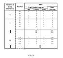
- FIG. 13is the LBA-PBA Map Table with striping for the layout shown in FIG. 12 according to an embodiment of the present invention.
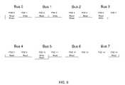
- FIG. 1shows an exemplary architecture that accommodates a very large number of flash arrays to achieve large capacities according to an embodiment of the present invention.
- the systemcomprises a number of Flash DMA, or Direct Memory Access, Engines (FDEs) 101 .
- a Flash DMA Engine (FDE)is basically an intelligent DMA controller that facilitates high speed data transfers to/from a group of flash memory devices.
- the systemalso contains a set of flash buses 102 , which is a bus interface used by the FDE to connect to the flash memory devices.
- flash array boards103 can be added.
- An expansion boardis essentially a memory board that consists of a pool of flash memory devices for additional storage and a Flash Buffer Controller 104 for communicating to the Flash DMA Engine.
- the Flash Buffer Controlleris a controller that drives the flash bus and translates the command signals from the FDEs into native flash commands that can be understood by the target flash chip.
- the number of buses/enginescan be increased/decreased according to the required performance, cost, and storage capacity of the system.
- the flash array organizationcomprises a set of Flash DMA Engines controlling multiple flash devices across a set of flash buses.
- the set of flash devices assigned to a particular flash busis called a “flash array bank”.
- Each bankcan be partitioned into any number of flash array banks with the Flash DMA Engines sharing a flash bus. For example in FIG. 1 , it is shown that a group of n number of Flash DMA Engines, such as group 105 , shares a single Flash Bus 0 106 .
- Each Flash DMA Engineis assigned to control a set of flash devices. This set of flash devices is said to belong to a flash array bank interleave. In addition, each flash device within this interleave is said to belong to a different flash group. From FIG. 1 , all flash chips labeled ‘A 0 ’ within flash array bank interleave 107 is controlled by Flash DMA Engine A 0 and each of the flash device within this interleave belongs to a different group. For example, the first flash device A 0 108 belongs to Group 0 , second flash device A 0 109 belongs to Group 1 , and so on.
- Bus interleavingis the transfer of data to/from flash devices using the different flash buses.
- the flash array bank interleaving methodis the transfer of data to/from flash devices belonging to the same bus but in different Flash DMA Engines.
- group interleavingis the transfer of data by a certain Flash DMA Engines to/from different flash devices it controls.
- the main advantage of implementing the bus interleaving methodis that the flash access is done in parallel utilizing the different flash buses, i.e. Flash Bus 0 , Flash Bus 1 , Flash Bus 2 , and so on.
- Flash Bus 0Flash Bus 0
- Flash Bus 1Flash Bus 1
- Flash Bus 2Flash Bus 2
- Each Flash DMA Engineuses a different flash bus in order to achieve parallel operations.
- Flash array bank interleavinghas parallel operations during flash access by utilizing the busy signal status of the active flash bus.
- one engine(FDE A 0 , where FDE stands for Flash DMA Engine, the term FDE and DMA Engine is used interchangeably in this document) is writing data to a flash device (flash device A 0 ) while FDE A 0 is waiting for the command completion, other FDE of different bank interleave, e.g., FDE A 1 , can access Flash Bus 0 and send out a command to a different target flash device such as flash device A 1 . Accordingly, group interleaving performs parallel operations by having a specific FDE send multiple commands to different flash devices it controls. As an example, one engine (FDE A 0 ) sends a command to a flash device A 0 of Group 0 .
- FDE A 0While FDE A 0 is waiting for the command to be completed and the flash bus is temporarily idle, FDE A 0 can send another command to a flash device in another group, e.g., flash device A 0 of Group 1 , in order to achieve optimum data transfer.
- FDE A 0can send another command to a flash device in another group, e.g., flash device A 0 of Group 1 , in order to achieve optimum data transfer.
- flash devicesare accessed using different flash bus (bus interleaving), then using different Flash DMA Engine (flash array bank interleaving) and lastly different group (group interleaving).
- flash DMA Engineflash array bank interleaving
- group interleavinggroup interleaving
- Another feature of new flash devicesis its multi-bank capability. A single flash device is sub-divided into four (4) banks wherein parallel operation can occur. In a Multi-Bank operation, an FDE can target up to four (4) different blocks in a target flash device and up to four (4) blocks can be erased and/or programmed using a single request.
- a mapping schemethat considers all these capabilities must be created.
- a section sizeis defined to be the minimum relocatable area. Assuming an LBA size is 512 bytes and the section size is 4 KB, only one entry is needed for every eight (8) LBAs.
- the section sizeis primarily limited by the native page size of a flash device. A page is smaller than the minimum erase size used for erasing data in a flash block. In the example shown, the minimum erase size used is equal to the flash block size.
- a flash blockis made up of multiple pages. It is always a multiple of this page size since a NAND flash is usually programmed on a per page basis.
- section sizeis the minimum relocatable region, when only five (5) LBAs are updated, the other three (3) LBAs must be relocated together with the new data. Smaller section would therefore lead to more flexibility but larger overhead to maintain the LBA-PBA mapping.
- a typical OS or Operating Systemusually accesses the media in larger blocks like 4 KB.
- the choice of the section sizedepends largely on how the host accesses the media. The larger the host access is, the more acceptable it is to use large section size to minimize the LBA-PBA mapping without suffering from the need to relocate unmodified data. Taking the concept wherein applications for rotating drives tend to optimize sequential access, this system as illustrated in FIG. 1 should take advantage of this and optimize for sequential access. Therefore, an exemplary ideal layout is illustrated in FIG. 2 .
- FIG. 2is a sample physical layout of data sections according to an embodiment of the present invention.
- the system shown in FIG. 2has sixteen (16) DMA Engines with two (2) engines sharing a bus. Each engine also controls two (2) flash devices for a total of thirty-two (32) flash devices.
- a sectionconsists of eight (8) LBAs. As can be seen from FIG. 2 , consecutive sections are distributed all throughout the entire flash arrays taking advantage of bus interleaves, then engine, interleaves, then group interleaves.
- mappingassures that the system will fetch the data in the most efficient or parallel way, taking advantage of the bus interleaving then bank interleaving and then group interleaving. But as noted before, due to the inherent characteristic of flash devices requiring erase cycles before writing new data, write operations will trigger the data to be relocated to new locations that have been previously erased (to save on erase cycles).
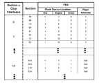
- FIG. 3is the LBA-PBA Map Table for the layout shown in FIG. 2 according to an embodiment of the present invention.
- FIG. 3shows how the LBA-PBA Map Table will look like based on the FIG. 2 layout.
- a sectionconsists of a group of LBAs.
- a section(corresponding to a row in the table) consists of eight (8) LBAs.
- the PBA stored herecontains the information for both the location of the flash device, uniquely identified using its engine number (bus number was added to illustrate bus interleaving but each engine is associated with only one bus) and group number, and the address within the flash device. From FIG.
- Section 0 301is located at Dev 0 , which has a unique address Bus 0 , Engine 0 , Group 0 and is in address 0 within that flash device.
- Section 1 302is located at Dev 2 , which has a unique address Bus 1 , Engine 2 , Group 0 and is in address 0 within that flash device.
- Section 61 303is located at Dev 27 , which has a unique address Bus 5 , Engine 11 , Group 1 and is in address 0x08 within that flash device. Assuming the flash is addressable every 512 bytes and a section is 4 KB in size, address 0x08 represents the second physical section (or the second 4 KB unit) within a flash device, address 0x10 the third physical section (or the third 4 KB unit) and so on.
- the 512 byte addressable unitmeans that every flash address represents 512 bytes so address 0x00 is the first 512 bytes, address 0x01 the second 512 bytes, and so on.
- the 512 byte addressable unitis just an arbitrary value for the system, it can be byte addressable leading to address 0x0000-0x0FFF representing the first 4 KB and address 0x1000-0x1FFF the next 4 KB.
- Mappingalso plays a major role to look up target physical locations for bad block management, for wear-leveling and most importantly for write operations.
- write operationsinstead of writing the new data in its old physical location, an erased physical location is obtained and the logical block is remapped there to save an erased cycle. Determining the new physical location is dependent on the current load of the system.
- the illustrated storage systemworks in the most optimum way when it takes advantage of the parallel operations it can execute at a given time with the bus interleaving being the most beneficial (then engine interleaving, then group interleaving). That means that whenever the system needs to determine a new physical location, it must take this into consideration.
- FIG. 4is a physical layout with erased sections according to an embodiment of the present invention.
- FIG. 4shows the distributed erased sections of the system. These erased sections will be the ones used when a write request need a new location. Only a small amount of the total storage needs to be reserved, this area can be used in conjunction with bad block replacements. The reserved amount depends on the capacity of the drive and the frequency of write requests it is subjected to. For a 60 GB drive, a 2-3% area or about 1-2 GB is efficient enough to provide erased sections as demanded with the stale blocks erased in the background.
- the location of the free sectionsneeds only to be distributed to all the flash arrays in the system and can be distributed in anyway within the flash device since access time within a flash is unaffected by its location. However, for flash devices offering multi-bank support, a flash device is divided into different banks with concurrent operation capability. For this case, the reserved pre-erased sections are distributed to the different banks of a flash chip to take advantage of the concurrent operation feature.
- FIG. 5is a block diagram illustrating how sections are placed to its new location when a write request is issued for that data section according to an embodiment of the present invention. Due to the write request for LBAs 0 - 23 , sections 0 - 2 , which holds this data, was relocated from its previous location 501 to the previously erased sections 502 . This would mean that when the host reads this data, it is still fetched in parallel as before. So not only will this approach increase efficiency during the write operation, it was also able to provide efficient access for future read operations of this data.
- the important thingis to spread out the data to different flash chips to take advantage of parallel access.
- the drive itselfis optimized for sequential access (as seen in FIG. 2 ) but as the host issues the write requests, the flash based system quickly adopts to the current load.
- the placement policywould force all the write requests to spread evenly across the entire system. As a consequence of spreading the locations, all consecutive requests would naturally go to different flash chips. In a typical scenario wherein related requests are done together, future reads to this data would also be optimized since related blocks would probably be spread out. How optimized the consequent layout would be largely dependent on how the Host issues its write requests. In a single process, this would be most optimized since requests are being generated by one source only. In a multi-user/process environment, requests come from different sources and the Host typically interleaves this. But even so, the placement policy would still be able to spread out related blocks although not as efficient since it is interleaved with other requests.
- FIG. 6shows the typical process when doing writes to flash devices. Basically whenever the system needs to write data to the flash array 601 , it first determines the current load of the FDE to determine which FDE has the least write request 602 to see where to put the new data. If a free section is not available, the system may force erasure of invalid blocks 604 and determine the next target FDE 605 . If a free section is available 603 , the system may get a free section for that FDE 606 . The system may update an LBA-PBA Map Table to reflect the new location 607 and queue up a write request 608 . In addition to determining the FDE, it can also determine to which flash device controlled by that FDE is optimum.
- target sectionscan also consider this. For example, if there is a request for Flash Dev 4 targeting Bank 0 , it can prioritize a request for Bank 1 of that flash device. This is of course after bus, engine and group prioritization.
- FIG. 7shows a simple way of listing all the available erased sections that can be utilized per engine for easy fetching of new locations. It holds the physical location 701 , which contains all the needed information like the FDE number, group location, and block address within the chip. Additionally, it contains the section index 702 , which is the next free section within a flash block. For simplicity and because of certain flash chips limitation that pages within a flash block can be programmed sequentially only, this index will just increment from zero (0) (entire flash block is erased) to the maximum index (three (3) if there are four (4) sections in a block. For example, a 4 KB section in a 16 KB block). So if only one section is needed, the index will just be incremented but if an entire block is needed, only the free entry with Section 0 can be utilized.
- FIG. 8shows a sample snapshot of the queue operations waiting for each Flash DMA Engine.
- the placement policywill determine what physical locations are prioritized. The easiest way is just to do a round-robin scheme wherein the priority just rotates in a fixed manner (FDE 0 , 2 , 4 , . . . 14 , 1 , 3 . . . 15 for Group 0 flash devices then for Group 1 , etc). This assures that all write operations have been evenly distributed. The drawback on this is that it doesn't consider the other operations that the engines are currently working on and thus might cause some unwanted delays. This can be resolved by using some threshold in which if a certain engine has too much workload with respect to others, that engine will simply be skipped in the rotation. For example, if a particular engine has five (5) more entries than the minimum of all the engines, it will just be skipped in the rotation and the next will be given the workload.
- FIG. 9shows how the first two (2) write requests being added to the queue of Flash DMA Engine operations. It shows the fetching of free sections from their respective engines and using that section for the new write requests. Assuming no request has been finished, the queue may look like FIG. 10 after queuing up twenty (20) write requests evenly distributed through all DMA Engines.
- FIG. 11shows the flow on how to manage bad blocks.
- the systemmay determine if a free section is available 1120 . If no free section is available, then the system may force erasure of invalid blocks 1130 and determine the next target location 1140 .
- the flowmay get a free block to replace the bad block 1150 and an update the LBA-PBA Map Table to update the new location 1160 will be accomplished. Also, if any data is recovered, a write to the new block 1170 will also be accomplished.
- Stripingforces parallel access at a lower level compared to what a section size can provide.
- There are programmable parameters for stripingone is the stripe size and the other is the number of chip interleaves.
- Stripe sizemeans the number of contiguous LBAs in a chip before moving on to the next chip.
- Number of chip interleavesmeans the number of chips the stripe will be distributed.
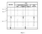
- FIG. 12shows the layout of FIG. 2 with striping support. Keeping section 1201 size to be 4 KB, stripe 1202 size is 1 KB and the number of chip interleaves 1203 is four (4). This means thirty-two (32) LBAs will be distributed to four (4) chips (eight (8) per section) with two (2) LBAs comprising a stripe.
- FIG. 13shows how the Map Table would look like. There would be four (4) related entries for a set of thirty-two (32) LBAs or four (4) sections. Size of the Map Table would still be the same but the LBAs will be striped to the different chips in each set.
- LBA 0 , 1would be in Dev 0 ; LBA 2 , 3 in Dev 2 ; LBA 4 , 5 in Dev 4 ; LBA 6 , 7 in Dev 6 ; LBA 8 , 9 back to Dev 0 and so on.
- Engines 0 , 2 , 4 , and 6are activated to get the eight (8) LBAs instead of just engine 0 when there is no striping.
- an apparatus for data storagecomprises: a plurality of flash buses; a plurality of DMA Engines coupled to at least two (2) of the plurality of flash buses; and a plurality of flash chips coupled to at least two (2) of the plurality of DMA Engines; wherein data access performance is improved by bus interleaving wherein one or more data is transferred to or from the plurality of flash chips using at least two (2) flash buses; wherein data access performance is improved by flash array bank interleaving wherein one or more data is transferred to or from the plurality of flash chips using at least two (2) DMA Engines; and wherein data access performance is improved by group interleaving wherein one or more data is transferred to or from the plurality of flash chips using at least two (2) flash chips.
- each of the plurality of flash chipsfurther comprises a plurality of sections; each section in the apparatus is operable to be accessed using a physical block address comprising a least significant portion, a second least significant portion, a third least significant portion, and a fourth least significant portion; wherein the least significant portion comprises an order according to the plurality of flash buses, the second least significant portion comprises an order according to a plurality of DMA Engines each coupled to a same flash bus, the third least significant portion comprises an order according to a plurality of flash chips each coupled to a same DMA Engine, and the fourth least significant portion comprises an order according to the plurality of sections in a same flash chip; and wherein a logical block address for host data access is mapped to a physical block address according to a system whereby host data access performance is improved.
- At least one section in at least one of the plurality of flash chipsis designated as free section; at least one free section is pre-erased as target for at least one data relocation whereby flash write performance and bad block replacement performance are improved according to the system.
- the systemmaps each logical block address to a physical block address in a linear mapping prior to the at least one data relocation; and the system designates a plurality of free sections evenly to each of the plurality of flash chips.
- the systemlocates a target for each of the at least one data relocation for write operation according to a current load represented in a system queue based on a priority comprising firstly locating a free section corresponding to a different flash bus, secondly locating a free section corresponding to a different DMA Engine coupled to a same flash bus, and thirdly locating a free section corresponding to a different flash chips coupled to a same DMA Engine; and the system locates a target for each of the at least one data relocation for bad block management based on a priority comprising firstly locating a free section corresponding to a same flash chips, secondly locating a free section corresponding to a different flash chips coupled to a same DMA Engine, and thirdly locating a section corresponding to a different DMA Engine coupled to a same flash bus.
- each sectionfurther comprises a plurality of strips; and the linear mapping further comprises one or more flash chip interleaves.
Landscapes
- Engineering & Computer Science (AREA)
- Theoretical Computer Science (AREA)
- Physics & Mathematics (AREA)
- General Engineering & Computer Science (AREA)
- General Physics & Mathematics (AREA)
- Information Retrieval, Db Structures And Fs Structures Therefor (AREA)
- Memory System Of A Hierarchy Structure (AREA)
- Techniques For Improving Reliability Of Storages (AREA)
Abstract
Description
Claims (7)
Priority Applications (6)
| Application Number | Priority Date | Filing Date | Title |
|---|---|---|---|
| US11/450,005US7506098B2 (en) | 2006-06-08 | 2006-06-08 | Optimized placement policy for solid state storage devices |
| TW096119243ATWI420307B (en) | 2006-06-08 | 2007-05-30 | Optimized placement policy for solid state storage devices |
| TW102144165ATWI540430B (en) | 2006-06-08 | 2007-05-30 | Method for data storage |
| PCT/US2007/070816WO2007146845A2 (en) | 2006-06-08 | 2007-06-08 | Configurable and scalable hybrid multi-tiered caching storage system |
| PCT/US2007/070660WO2007146756A2 (en) | 2006-06-08 | 2007-06-08 | Optimized placement policy for solid state storage devices |
| US12/323,461US8010740B2 (en) | 2006-06-08 | 2008-11-25 | Optimizing memory operations in an electronic storage device |
Applications Claiming Priority (1)
| Application Number | Priority Date | Filing Date | Title |
|---|---|---|---|
| US11/450,005US7506098B2 (en) | 2006-06-08 | 2006-06-08 | Optimized placement policy for solid state storage devices |
Related Parent Applications (1)
| Application Number | Title | Priority Date | Filing Date |
|---|---|---|---|
| US11/450,023Continuation-In-PartUS7613876B2 (en) | 2006-06-08 | 2006-06-08 | Hybrid multi-tiered caching storage system |
Related Child Applications (1)
| Application Number | Title | Priority Date | Filing Date |
|---|---|---|---|
| US12/323,461Continuation-In-PartUS8010740B2 (en) | 2006-06-08 | 2008-11-25 | Optimizing memory operations in an electronic storage device |
Publications (2)
| Publication Number | Publication Date |
|---|---|
| US20070288686A1 US20070288686A1 (en) | 2007-12-13 |
| US7506098B2true US7506098B2 (en) | 2009-03-17 |
Family
ID=38823270
Family Applications (1)
| Application Number | Title | Priority Date | Filing Date |
|---|---|---|---|
| US11/450,005Expired - Fee RelatedUS7506098B2 (en) | 2006-06-08 | 2006-06-08 | Optimized placement policy for solid state storage devices |
Country Status (3)
| Country | Link |
|---|---|
| US (1) | US7506098B2 (en) |
| TW (2) | TWI540430B (en) |
| WO (1) | WO2007146756A2 (en) |
Cited By (39)
| Publication number | Priority date | Publication date | Assignee | Title |
|---|---|---|---|---|
| US20090077429A1 (en)* | 2007-09-13 | 2009-03-19 | Samsung Electronics Co., Ltd. | Memory system and wear-leveling method thereof |
| US20100262764A1 (en)* | 2009-04-14 | 2010-10-14 | Chao-Yin Liu | Method for accessing storage apparatus and related control circuit |
| US20100318719A1 (en)* | 2009-06-12 | 2010-12-16 | Micron Technology, Inc. | Methods, memory controllers and devices for wear leveling a memory |
| US20110082967A1 (en)* | 2009-10-05 | 2011-04-07 | Deshkar Shekhar S | Data Caching In Non-Volatile Memory |
| US8447920B1 (en)* | 2010-06-29 | 2013-05-21 | Western Digital Technologies, Inc. | System and method for managing data access in non-volatile memory |
| US20130227246A1 (en)* | 2012-02-23 | 2013-08-29 | Kabushiki Kaisha Toshiba | Management information generating method, logical block constructing method, and semiconductor memory device |
| US8593866B2 (en)* | 2011-11-11 | 2013-11-26 | Sandisk Technologies Inc. | Systems and methods for operating multi-bank nonvolatile memory |
| US8843694B2 (en) | 2007-02-22 | 2014-09-23 | Conversant Intellectual Property Management Inc. | System and method of page buffer operation for memory devices |
| US8880780B2 (en) | 2007-02-22 | 2014-11-04 | Conversant Intellectual Property Management Incorporated | Apparatus and method for using a page buffer of a memory device as a temporary cache |
| US9003068B2 (en) | 2012-07-12 | 2015-04-07 | International Business Machines Corporation | Service channel for connecting a host computer to peripheral devices |
| US9043669B1 (en) | 2012-05-18 | 2015-05-26 | Bitmicro Networks, Inc. | Distributed ECC engine for storage media |
| US9099187B2 (en) | 2009-09-14 | 2015-08-04 | Bitmicro Networks, Inc. | Reducing erase cycles in an electronic storage device that uses at least one erase-limited memory device |
| US9372755B1 (en) | 2011-10-05 | 2016-06-21 | Bitmicro Networks, Inc. | Adaptive power cycle sequences for data recovery |
| US9400617B2 (en) | 2013-03-15 | 2016-07-26 | Bitmicro Networks, Inc. | Hardware-assisted DMA transfer with dependency table configured to permit-in parallel-data drain from cache without processor intervention when filled or drained |
| US9423457B2 (en) | 2013-03-14 | 2016-08-23 | Bitmicro Networks, Inc. | Self-test solution for delay locked loops |
| US9430386B2 (en) | 2013-03-15 | 2016-08-30 | Bitmicro Networks, Inc. | Multi-leveled cache management in a hybrid storage system |
| US9501436B1 (en) | 2013-03-15 | 2016-11-22 | Bitmicro Networks, Inc. | Multi-level message passing descriptor |
| US9672178B1 (en) | 2013-03-15 | 2017-06-06 | Bitmicro Networks, Inc. | Bit-mapped DMA transfer with dependency table configured to monitor status so that a processor is not rendered as a bottleneck in a system |
| US9720603B1 (en) | 2013-03-15 | 2017-08-01 | Bitmicro Networks, Inc. | IOC to IOC distributed caching architecture |
| US9734067B1 (en) | 2013-03-15 | 2017-08-15 | Bitmicro Networks, Inc. | Write buffering |
| US9798688B1 (en) | 2013-03-15 | 2017-10-24 | Bitmicro Networks, Inc. | Bus arbitration with routing and failover mechanism |
| US9811461B1 (en) | 2014-04-17 | 2017-11-07 | Bitmicro Networks, Inc. | Data storage system |
| US9842024B1 (en) | 2013-03-15 | 2017-12-12 | Bitmicro Networks, Inc. | Flash electronic disk with RAID controller |
| US9858084B2 (en) | 2013-03-15 | 2018-01-02 | Bitmicro Networks, Inc. | Copying of power-on reset sequencer descriptor from nonvolatile memory to random access memory |
| US9875205B1 (en) | 2013-03-15 | 2018-01-23 | Bitmicro Networks, Inc. | Network of memory systems |
| US9916213B1 (en) | 2013-03-15 | 2018-03-13 | Bitmicro Networks, Inc. | Bus arbitration with routing and failover mechanism |
| US9934045B1 (en) | 2013-03-15 | 2018-04-03 | Bitmicro Networks, Inc. | Embedded system boot from a storage device |
| US9952991B1 (en) | 2014-04-17 | 2018-04-24 | Bitmicro Networks, Inc. | Systematic method on queuing of descriptors for multiple flash intelligent DMA engine operation |
| US9971524B1 (en) | 2013-03-15 | 2018-05-15 | Bitmicro Networks, Inc. | Scatter-gather approach for parallel data transfer in a mass storage system |
| US10025736B1 (en) | 2014-04-17 | 2018-07-17 | Bitmicro Networks, Inc. | Exchange message protocol message transmission between two devices |
| US10042792B1 (en) | 2014-04-17 | 2018-08-07 | Bitmicro Networks, Inc. | Method for transferring and receiving frames across PCI express bus for SSD device |
| US10055150B1 (en) | 2014-04-17 | 2018-08-21 | Bitmicro Networks, Inc. | Writing volatile scattered memory metadata to flash device |
| US10078604B1 (en) | 2014-04-17 | 2018-09-18 | Bitmicro Networks, Inc. | Interrupt coalescing |
| US10120586B1 (en) | 2007-11-16 | 2018-11-06 | Bitmicro, Llc | Memory transaction with reduced latency |
| US10133686B2 (en) | 2009-09-07 | 2018-11-20 | Bitmicro Llc | Multilevel memory bus system |
| US10149399B1 (en) | 2009-09-04 | 2018-12-04 | Bitmicro Llc | Solid state drive with improved enclosure assembly |
| US10489318B1 (en) | 2013-03-15 | 2019-11-26 | Bitmicro Networks, Inc. | Scatter-gather approach for parallel data transfer in a mass storage system |
| US10552050B1 (en) | 2017-04-07 | 2020-02-04 | Bitmicro Llc | Multi-dimensional computer storage system |
| US11397529B2 (en) | 2019-12-25 | 2022-07-26 | Samsung Electronics Co., Ltd. | Method and device for determining strategy for data placement within SSD |
Families Citing this family (61)
| Publication number | Priority date | Publication date | Assignee | Title |
|---|---|---|---|---|
| KR20050022798A (en)* | 2003-08-30 | 2005-03-08 | 주식회사 이즈텍 | A system for analyzing bio chips using gene ontology, and a method thereof |
| US8438328B2 (en) | 2008-02-21 | 2013-05-07 | Google Inc. | Emulation of abstracted DIMMs using abstracted DRAMs |
| US7609567B2 (en) | 2005-06-24 | 2009-10-27 | Metaram, Inc. | System and method for simulating an aspect of a memory circuit |
| US8090897B2 (en) | 2006-07-31 | 2012-01-03 | Google Inc. | System and method for simulating an aspect of a memory circuit |
| US9507739B2 (en) | 2005-06-24 | 2016-11-29 | Google Inc. | Configurable memory circuit system and method |
| US20080028136A1 (en) | 2006-07-31 | 2008-01-31 | Schakel Keith R | Method and apparatus for refresh management of memory modules |
| US8796830B1 (en) | 2006-09-01 | 2014-08-05 | Google Inc. | Stackable low-profile lead frame package |
| US8089795B2 (en) | 2006-02-09 | 2012-01-03 | Google Inc. | Memory module with memory stack and interface with enhanced capabilities |
| US20080082763A1 (en) | 2006-10-02 | 2008-04-03 | Metaram, Inc. | Apparatus and method for power management of memory circuits by a system or component thereof |
| US8359187B2 (en) | 2005-06-24 | 2013-01-22 | Google Inc. | Simulating a different number of memory circuit devices |
| US7580312B2 (en) | 2006-07-31 | 2009-08-25 | Metaram, Inc. | Power saving system and method for use with a plurality of memory circuits |
| US8041881B2 (en) | 2006-07-31 | 2011-10-18 | Google Inc. | Memory device with emulated characteristics |
| US8327104B2 (en) | 2006-07-31 | 2012-12-04 | Google Inc. | Adjusting the timing of signals associated with a memory system |
| US8130560B1 (en) | 2006-11-13 | 2012-03-06 | Google Inc. | Multi-rank partial width memory modules |
| US8060774B2 (en) | 2005-06-24 | 2011-11-15 | Google Inc. | Memory systems and memory modules |
| US8397013B1 (en) | 2006-10-05 | 2013-03-12 | Google Inc. | Hybrid memory module |
| US7386656B2 (en) | 2006-07-31 | 2008-06-10 | Metaram, Inc. | Interface circuit system and method for performing power management operations in conjunction with only a portion of a memory circuit |
| US8111566B1 (en) | 2007-11-16 | 2012-02-07 | Google, Inc. | Optimal channel design for memory devices for providing a high-speed memory interface |
| US8244971B2 (en) | 2006-07-31 | 2012-08-14 | Google Inc. | Memory circuit system and method |
| US8081474B1 (en) | 2007-12-18 | 2011-12-20 | Google Inc. | Embossed heat spreader |
| US9542352B2 (en) | 2006-02-09 | 2017-01-10 | Google Inc. | System and method for reducing command scheduling constraints of memory circuits |
| US10013371B2 (en) | 2005-06-24 | 2018-07-03 | Google Llc | Configurable memory circuit system and method |
| US8055833B2 (en) | 2006-10-05 | 2011-11-08 | Google Inc. | System and method for increasing capacity, performance, and flexibility of flash storage |
| US8335894B1 (en) | 2008-07-25 | 2012-12-18 | Google Inc. | Configurable memory system with interface circuit |
| US8077535B2 (en) | 2006-07-31 | 2011-12-13 | Google Inc. | Memory refresh apparatus and method |
| US8386722B1 (en) | 2008-06-23 | 2013-02-26 | Google Inc. | Stacked DIMM memory interface |
| US7392338B2 (en) | 2006-07-31 | 2008-06-24 | Metaram, Inc. | Interface circuit system and method for autonomously performing power management operations in conjunction with a plurality of memory circuits |
| US9171585B2 (en) | 2005-06-24 | 2015-10-27 | Google Inc. | Configurable memory circuit system and method |
| US7590796B2 (en) | 2006-07-31 | 2009-09-15 | Metaram, Inc. | System and method for power management in memory systems |
| WO2007028109A2 (en) | 2005-09-02 | 2007-03-08 | Metaram, Inc. | Methods and apparatus of stacking drams |
| US9632929B2 (en) | 2006-02-09 | 2017-04-25 | Google Inc. | Translating an address associated with a command communicated between a system and memory circuits |
| US7724589B2 (en) | 2006-07-31 | 2010-05-25 | Google Inc. | System and method for delaying a signal communicated from a system to at least one of a plurality of memory circuits |
| US7904639B2 (en)* | 2006-08-22 | 2011-03-08 | Mosaid Technologies Incorporated | Modular command structure for memory and memory system |
| US8209479B2 (en) | 2007-07-18 | 2012-06-26 | Google Inc. | Memory circuit system and method |
| US8080874B1 (en) | 2007-09-14 | 2011-12-20 | Google Inc. | Providing additional space between an integrated circuit and a circuit board for positioning a component therebetween |
| KR101083673B1 (en)* | 2008-10-01 | 2011-11-16 | 주식회사 하이닉스반도체 | Semiconductor storage system and its control method |
| US8275929B2 (en)* | 2008-10-29 | 2012-09-25 | Macronix International Co., Ltd. | Memory and operating method thereof |
| JP5323199B2 (en) | 2009-02-12 | 2013-10-23 | 株式会社東芝 | Memory system and memory system control method |
| US20100287217A1 (en)* | 2009-04-08 | 2010-11-11 | Google Inc. | Host control of background garbage collection in a data storage device |
| US20100262979A1 (en)* | 2009-04-08 | 2010-10-14 | Google Inc. | Circular command queues for communication between a host and a data storage device |
| US8205037B2 (en)* | 2009-04-08 | 2012-06-19 | Google Inc. | Data storage device capable of recognizing and controlling multiple types of memory chips operating at different voltages |
| US8433845B2 (en)* | 2009-04-08 | 2013-04-30 | Google Inc. | Data storage device which serializes memory device ready/busy signals |
| JP5532671B2 (en)* | 2009-05-08 | 2014-06-25 | ソニー株式会社 | Data storage system and data storage method, execution device and control method, and control device and control method |
| DE202010017690U1 (en) | 2009-06-09 | 2012-05-29 | Google, Inc. | Programming dimming terminating resistor values |
| EP2507700A1 (en)* | 2009-12-04 | 2012-10-10 | Marvell World Trade Ltd. | Virtualization of storage devices |
| US8443167B1 (en) | 2009-12-16 | 2013-05-14 | Western Digital Technologies, Inc. | Data storage device employing a run-length mapping table and a single address mapping table |
| US8194340B1 (en) | 2010-03-18 | 2012-06-05 | Western Digital Technologies, Inc. | Disk drive framing write data with in-line mapping data during write operations |
| US8699185B1 (en) | 2012-12-10 | 2014-04-15 | Western Digital Technologies, Inc. | Disk drive defining guard bands to support zone sequentiality when butterfly writing shingled data tracks |
| US9330715B1 (en) | 2010-03-22 | 2016-05-03 | Western Digital Technologies, Inc. | Mapping of shingled magnetic recording media |
| US8856438B1 (en) | 2011-12-09 | 2014-10-07 | Western Digital Technologies, Inc. | Disk drive with reduced-size translation table |
| US8687306B1 (en) | 2010-03-22 | 2014-04-01 | Western Digital Technologies, Inc. | Systems and methods for improving sequential data rate performance using sorted data zones |
| US8693133B1 (en) | 2010-03-22 | 2014-04-08 | Western Digital Technologies, Inc. | Systems and methods for improving sequential data rate performance using sorted data zones for butterfly format |
| US8615640B2 (en) | 2011-03-17 | 2013-12-24 | Lsi Corporation | System and method to efficiently schedule and/or commit write data to flash based SSDs attached to an array controller |
| US8793429B1 (en) | 2011-06-03 | 2014-07-29 | Western Digital Technologies, Inc. | Solid-state drive with reduced power up time |
| US9213493B1 (en) | 2011-12-16 | 2015-12-15 | Western Digital Technologies, Inc. | Sorted serpentine mapping for storage drives |
| US8819367B1 (en) | 2011-12-19 | 2014-08-26 | Western Digital Technologies, Inc. | Accelerated translation power recovery |
| US8953269B1 (en) | 2014-07-18 | 2015-02-10 | Western Digital Technologies, Inc. | Management of data objects in a data object zone |
| US9875055B1 (en) | 2014-08-04 | 2018-01-23 | Western Digital Technologies, Inc. | Check-pointing of metadata |
| CN108932106B (en)* | 2017-05-26 | 2021-07-02 | 上海宝存信息科技有限公司 | Solid state disk access method and device using same |
| US10635331B2 (en) | 2017-07-05 | 2020-04-28 | Western Digital Technologies, Inc. | Distribution of logical-to-physical address entries across bank groups |
| JP2022147448A (en)* | 2021-03-23 | 2022-10-06 | キオクシア株式会社 | Memory system and data management method |
Citations (4)
| Publication number | Priority date | Publication date | Assignee | Title |
|---|---|---|---|---|
| US5822251A (en)* | 1997-08-25 | 1998-10-13 | Bit Microsystems, Inc. | Expandable flash-memory mass-storage using shared buddy lines and intermediate flash-bus between device-specific buffers and flash-intelligent DMA controllers |
| US20020141244A1 (en)* | 2000-11-30 | 2002-10-03 | Bruce Ricardo H. | Parallel erase operations in memory systems |
| US20030217202A1 (en)* | 2002-05-15 | 2003-11-20 | M-Systems Flash Disk Pioneers Ltd. | Method for improving performance of a flash-based storage system using specialized flash controllers |
| US20040073721A1 (en)* | 2002-10-10 | 2004-04-15 | Koninklijke Philips Electronics N.V. | DMA Controller for USB and like applications |
Family Cites Families (4)
| Publication number | Priority date | Publication date | Assignee | Title |
|---|---|---|---|---|
| EP0804008B1 (en)* | 1996-04-26 | 2006-11-15 | Texas Instruments Incorporated | Apparatus for data packet transfer control |
| JP2870530B1 (en)* | 1997-10-30 | 1999-03-17 | 日本電気株式会社 | Stack module interposer and stack module |
| US20050114587A1 (en)* | 2003-11-22 | 2005-05-26 | Super Talent Electronics Inc. | ExpressCard with On-Card Flash Memory with Shared Flash-Control Bus but Separate Ready Lines |
| US7484016B2 (en)* | 2004-06-30 | 2009-01-27 | Intel Corporation | Apparatus and method for high performance volatile disk drive memory access using an integrated DMA engine |
- 2006
- 2006-06-08USUS11/450,005patent/US7506098B2/ennot_activeExpired - Fee Related
- 2007
- 2007-05-30TWTW102144165Apatent/TWI540430B/ennot_activeIP Right Cessation
- 2007-05-30TWTW096119243Apatent/TWI420307B/ennot_activeIP Right Cessation
- 2007-06-08WOPCT/US2007/070660patent/WO2007146756A2/enactiveApplication Filing
Patent Citations (4)
| Publication number | Priority date | Publication date | Assignee | Title |
|---|---|---|---|---|
| US5822251A (en)* | 1997-08-25 | 1998-10-13 | Bit Microsystems, Inc. | Expandable flash-memory mass-storage using shared buddy lines and intermediate flash-bus between device-specific buffers and flash-intelligent DMA controllers |
| US20020141244A1 (en)* | 2000-11-30 | 2002-10-03 | Bruce Ricardo H. | Parallel erase operations in memory systems |
| US20030217202A1 (en)* | 2002-05-15 | 2003-11-20 | M-Systems Flash Disk Pioneers Ltd. | Method for improving performance of a flash-based storage system using specialized flash controllers |
| US20040073721A1 (en)* | 2002-10-10 | 2004-04-15 | Koninklijke Philips Electronics N.V. | DMA Controller for USB and like applications |
Cited By (57)
| Publication number | Priority date | Publication date | Assignee | Title |
|---|---|---|---|---|
| US8843694B2 (en) | 2007-02-22 | 2014-09-23 | Conversant Intellectual Property Management Inc. | System and method of page buffer operation for memory devices |
| US8886871B2 (en) | 2007-02-22 | 2014-11-11 | Conversant Intellectual Property Management Incorporated | Apparatus and method of page program operation for memory devices with mirror back-up of data |
| US8880780B2 (en) | 2007-02-22 | 2014-11-04 | Conversant Intellectual Property Management Incorporated | Apparatus and method for using a page buffer of a memory device as a temporary cache |
| US9251015B2 (en) | 2007-09-13 | 2016-02-02 | Samsung Electronics Co., Ltd. | Memory system providing wear-leveling by allocating memory blocks among groups |
| US9229805B2 (en)* | 2007-09-13 | 2016-01-05 | Samsung Electronics Co., Ltd. | Memory system and wear-leveling method thereof based on erasures and error correction data |
| US20090077429A1 (en)* | 2007-09-13 | 2009-03-19 | Samsung Electronics Co., Ltd. | Memory system and wear-leveling method thereof |
| US10120586B1 (en) | 2007-11-16 | 2018-11-06 | Bitmicro, Llc | Memory transaction with reduced latency |
| TWI408689B (en)* | 2009-04-14 | 2013-09-11 | Jmicron Technology Corp | Method for accessing storage apparatus and related control circuit |
| US20100262764A1 (en)* | 2009-04-14 | 2010-10-14 | Chao-Yin Liu | Method for accessing storage apparatus and related control circuit |
| US20100318719A1 (en)* | 2009-06-12 | 2010-12-16 | Micron Technology, Inc. | Methods, memory controllers and devices for wear leveling a memory |
| US10149399B1 (en) | 2009-09-04 | 2018-12-04 | Bitmicro Llc | Solid state drive with improved enclosure assembly |
| US10133686B2 (en) | 2009-09-07 | 2018-11-20 | Bitmicro Llc | Multilevel memory bus system |
| US10082966B1 (en) | 2009-09-14 | 2018-09-25 | Bitmicro Llc | Electronic storage device |
| US9484103B1 (en)* | 2009-09-14 | 2016-11-01 | Bitmicro Networks, Inc. | Electronic storage device |
| US9099187B2 (en) | 2009-09-14 | 2015-08-04 | Bitmicro Networks, Inc. | Reducing erase cycles in an electronic storage device that uses at least one erase-limited memory device |
| US9003159B2 (en) | 2009-10-05 | 2015-04-07 | Marvell World Trade Ltd. | Data caching in non-volatile memory |
| US20110082967A1 (en)* | 2009-10-05 | 2011-04-07 | Deshkar Shekhar S | Data Caching In Non-Volatile Memory |
| US8825947B1 (en) | 2010-06-29 | 2014-09-02 | Western Digital Technologies, Inc. | System and method for managing data access in non-volatile memory |
| US8447920B1 (en)* | 2010-06-29 | 2013-05-21 | Western Digital Technologies, Inc. | System and method for managing data access in non-volatile memory |
| US10180887B1 (en) | 2011-10-05 | 2019-01-15 | Bitmicro Llc | Adaptive power cycle sequences for data recovery |
| US9372755B1 (en) | 2011-10-05 | 2016-06-21 | Bitmicro Networks, Inc. | Adaptive power cycle sequences for data recovery |
| US8593866B2 (en)* | 2011-11-11 | 2013-11-26 | Sandisk Technologies Inc. | Systems and methods for operating multi-bank nonvolatile memory |
| US8924636B2 (en)* | 2012-02-23 | 2014-12-30 | Kabushiki Kaisha Toshiba | Management information generating method, logical block constructing method, and semiconductor memory device |
| US20130227246A1 (en)* | 2012-02-23 | 2013-08-29 | Kabushiki Kaisha Toshiba | Management information generating method, logical block constructing method, and semiconductor memory device |
| US9996419B1 (en) | 2012-05-18 | 2018-06-12 | Bitmicro Llc | Storage system with distributed ECC capability |
| US9043669B1 (en) | 2012-05-18 | 2015-05-26 | Bitmicro Networks, Inc. | Distributed ECC engine for storage media |
| US9003068B2 (en) | 2012-07-12 | 2015-04-07 | International Business Machines Corporation | Service channel for connecting a host computer to peripheral devices |
| US9423457B2 (en) | 2013-03-14 | 2016-08-23 | Bitmicro Networks, Inc. | Self-test solution for delay locked loops |
| US9977077B1 (en) | 2013-03-14 | 2018-05-22 | Bitmicro Llc | Self-test solution for delay locked loops |
| US9798688B1 (en) | 2013-03-15 | 2017-10-24 | Bitmicro Networks, Inc. | Bus arbitration with routing and failover mechanism |
| US10120694B2 (en) | 2013-03-15 | 2018-11-06 | Bitmicro Networks, Inc. | Embedded system boot from a storage device |
| US9858084B2 (en) | 2013-03-15 | 2018-01-02 | Bitmicro Networks, Inc. | Copying of power-on reset sequencer descriptor from nonvolatile memory to random access memory |
| US9875205B1 (en) | 2013-03-15 | 2018-01-23 | Bitmicro Networks, Inc. | Network of memory systems |
| US9916213B1 (en) | 2013-03-15 | 2018-03-13 | Bitmicro Networks, Inc. | Bus arbitration with routing and failover mechanism |
| US9934045B1 (en) | 2013-03-15 | 2018-04-03 | Bitmicro Networks, Inc. | Embedded system boot from a storage device |
| US9934160B1 (en) | 2013-03-15 | 2018-04-03 | Bitmicro Llc | Bit-mapped DMA and IOC transfer with dependency table comprising plurality of index fields in the cache for DMA transfer |
| US10489318B1 (en) | 2013-03-15 | 2019-11-26 | Bitmicro Networks, Inc. | Scatter-gather approach for parallel data transfer in a mass storage system |
| US9971524B1 (en) | 2013-03-15 | 2018-05-15 | Bitmicro Networks, Inc. | Scatter-gather approach for parallel data transfer in a mass storage system |
| US10423554B1 (en) | 2013-03-15 | 2019-09-24 | Bitmicro Networks, Inc | Bus arbitration with routing and failover mechanism |
| US9734067B1 (en) | 2013-03-15 | 2017-08-15 | Bitmicro Networks, Inc. | Write buffering |
| US10013373B1 (en) | 2013-03-15 | 2018-07-03 | Bitmicro Networks, Inc. | Multi-level message passing descriptor |
| US10210084B1 (en) | 2013-03-15 | 2019-02-19 | Bitmicro Llc | Multi-leveled cache management in a hybrid storage system |
| US10042799B1 (en) | 2013-03-15 | 2018-08-07 | Bitmicro, Llc | Bit-mapped DMA transfer with dependency table configured to monitor status so that a processor is not rendered as a bottleneck in a system |
| US9400617B2 (en) | 2013-03-15 | 2016-07-26 | Bitmicro Networks, Inc. | Hardware-assisted DMA transfer with dependency table configured to permit-in parallel-data drain from cache without processor intervention when filled or drained |
| US9430386B2 (en) | 2013-03-15 | 2016-08-30 | Bitmicro Networks, Inc. | Multi-leveled cache management in a hybrid storage system |
| US9501436B1 (en) | 2013-03-15 | 2016-11-22 | Bitmicro Networks, Inc. | Multi-level message passing descriptor |
| US9720603B1 (en) | 2013-03-15 | 2017-08-01 | Bitmicro Networks, Inc. | IOC to IOC distributed caching architecture |
| US9672178B1 (en) | 2013-03-15 | 2017-06-06 | Bitmicro Networks, Inc. | Bit-mapped DMA transfer with dependency table configured to monitor status so that a processor is not rendered as a bottleneck in a system |
| US9842024B1 (en) | 2013-03-15 | 2017-12-12 | Bitmicro Networks, Inc. | Flash electronic disk with RAID controller |
| US10078604B1 (en) | 2014-04-17 | 2018-09-18 | Bitmicro Networks, Inc. | Interrupt coalescing |
| US10055150B1 (en) | 2014-04-17 | 2018-08-21 | Bitmicro Networks, Inc. | Writing volatile scattered memory metadata to flash device |
| US10042792B1 (en) | 2014-04-17 | 2018-08-07 | Bitmicro Networks, Inc. | Method for transferring and receiving frames across PCI express bus for SSD device |
| US10025736B1 (en) | 2014-04-17 | 2018-07-17 | Bitmicro Networks, Inc. | Exchange message protocol message transmission between two devices |
| US9811461B1 (en) | 2014-04-17 | 2017-11-07 | Bitmicro Networks, Inc. | Data storage system |
| US9952991B1 (en) | 2014-04-17 | 2018-04-24 | Bitmicro Networks, Inc. | Systematic method on queuing of descriptors for multiple flash intelligent DMA engine operation |
| US10552050B1 (en) | 2017-04-07 | 2020-02-04 | Bitmicro Llc | Multi-dimensional computer storage system |
| US11397529B2 (en) | 2019-12-25 | 2022-07-26 | Samsung Electronics Co., Ltd. | Method and device for determining strategy for data placement within SSD |
Also Published As
| Publication number | Publication date |
|---|---|
| US20070288686A1 (en) | 2007-12-13 |
| WO2007146756A3 (en) | 2009-01-08 |
| TW201415223A (en) | 2014-04-16 |
| WO2007146756A2 (en) | 2007-12-21 |
| TW200807241A (en) | 2008-02-01 |
| TWI420307B (en) | 2013-12-21 |
| TWI540430B (en) | 2016-07-01 |
Similar Documents
| Publication | Publication Date | Title |
|---|---|---|
| US7506098B2 (en) | Optimized placement policy for solid state storage devices | |
| KR101516580B1 (en) | Controller, data storage device and data storage system having the same, and method thereof | |
| CN110998550B (en) | Memory addressing | |
| CN108121503B (en) | NandFlash address mapping and block management method | |
| US8010740B2 (en) | Optimizing memory operations in an electronic storage device | |
| JP5458419B2 (en) | Select memory block | |
| US9390004B2 (en) | Hybrid memory management | |
| EP2895958B1 (en) | Address mapping | |
| US8208322B2 (en) | Non-volatile memory control | |
| US6327639B1 (en) | Method and apparatus for storing location identification information within non-volatile memory devices | |
| US8452911B2 (en) | Synchronized maintenance operations in a multi-bank storage system | |
| US7487303B2 (en) | Flash memory device and associated data merge method | |
| US9110594B2 (en) | File management system for devices containing solid-state media | |
| TWI432965B (en) | Memory systems with a plurality of structures and methods for operating the same | |
| US20050172067A1 (en) | Mass storage accelerator | |
| US20200310669A1 (en) | Optimized handling of multiple copies in storage management | |
| KR101025375B1 (en) | Method of writing data in nonvolatile memory device and nonvolatile memory device performing same |
Legal Events
| Date | Code | Title | Description |
|---|---|---|---|
| AS | Assignment | Owner name:BITMICRO NETWORKS, CALIFORNIA Free format text:ASSIGNMENT OF ASSIGNORS INTEREST;ASSIGNORS:ARCEDERA, MARK;LANUZA, REYJAN;BABAYLAN, RITCHIE;REEL/FRAME:017999/0041 Effective date:20060608 | |
| STCF | Information on status: patent grant | Free format text:PATENTED CASE | |
| FPAY | Fee payment | Year of fee payment:4 | |
| FEPP | Fee payment procedure | Free format text:PAT HOLDER NO LONGER CLAIMS SMALL ENTITY STATUS, ENTITY STATUS SET TO UNDISCOUNTED (ORIGINAL EVENT CODE: STOL); ENTITY STATUS OF PATENT OWNER: LARGE ENTITY | |
| FPAY | Fee payment | Year of fee payment:8 | |
| AS | Assignment | Owner name:BITMICRO NETWORKS, INC., CALIFORNIA Free format text:ASSIGNMENT OF ASSIGNORS INTEREST;ASSIGNORS:ARCEDERA, MARK;LANUZA, REYJAN;BABAYLAN, RITCHIE;SIGNING DATES FROM 20170619 TO 20170704;REEL/FRAME:042889/0001 | |
| AS | Assignment | Owner name:BITMICRO LLC, SOUTH CAROLINA Free format text:ASSIGNMENT OF ASSIGNORS INTEREST;ASSIGNOR:BITMICRO NETWORKS, INC.;REEL/FRAME:043536/0407 Effective date:20170630 | |
| FEPP | Fee payment procedure | Free format text:MAINTENANCE FEE REMINDER MAILED (ORIGINAL EVENT CODE: REM.); ENTITY STATUS OF PATENT OWNER: LARGE ENTITY | |
| LAPS | Lapse for failure to pay maintenance fees | Free format text:PATENT EXPIRED FOR FAILURE TO PAY MAINTENANCE FEES (ORIGINAL EVENT CODE: EXP.); ENTITY STATUS OF PATENT OWNER: LARGE ENTITY | |
| STCH | Information on status: patent discontinuation | Free format text:PATENT EXPIRED DUE TO NONPAYMENT OF MAINTENANCE FEES UNDER 37 CFR 1.362 | |
| FP | Lapsed due to failure to pay maintenance fee | Effective date:20210317 |