US7505496B2 - Systems and methods for real-time compensation for non-linearity in optical sources for analog signal transmission - Google Patents
Systems and methods for real-time compensation for non-linearity in optical sources for analog signal transmissionDownload PDFInfo
- Publication number
- US7505496B2 US7505496B2US11/398,107US39810706AUS7505496B2US 7505496 B2US7505496 B2US 7505496B2US 39810706 AUS39810706 AUS 39810706AUS 7505496 B2US7505496 B2US 7505496B2
- Authority
- US
- United States
- Prior art keywords
- analog
- feedback
- correction loop
- feedback correction
- input current
- Prior art date
- Legal status (The legal status is an assumption and is not a legal conclusion. Google has not performed a legal analysis and makes no representation as to the accuracy of the status listed.)
- Active
Links
- 230000003287optical effectEffects0.000titleclaimsabstractdescription74
- 238000000034methodMethods0.000titleclaimsabstractdescription44
- 230000008054signal transmissionEffects0.000titleclaimsdescription16
- 238000012546transferMethods0.000claimsabstractdescription18
- 238000012937correctionMethods0.000claimsdescription54
- 230000006870functionEffects0.000claimsdescription18
- 239000004065semiconductorSubstances0.000claimsdescription7
- 230000005055memory storageEffects0.000claims3
- 238000012544monitoring processMethods0.000claims2
- 230000000694effectsEffects0.000abstractdescription4
- 230000001419dependent effectEffects0.000abstractdescription3
- 230000005540biological transmissionEffects0.000description7
- 230000003071parasitic effectEffects0.000description5
- 238000002310reflectometryMethods0.000description4
- 230000008033biological extinctionEffects0.000description3
- 238000002347injectionMethods0.000description3
- 239000007924injectionSubstances0.000description3
- 230000015556catabolic processEffects0.000description2
- 238000006731degradation reactionMethods0.000description2
- 238000010586diagramMethods0.000description2
- 239000000835fiberSubstances0.000description2
- 238000005259measurementMethods0.000description2
- 238000010521absorption reactionMethods0.000description1
- 238000013459approachMethods0.000description1
- 230000001413cellular effectEffects0.000description1
- 230000003247decreasing effectEffects0.000description1
- 238000013461designMethods0.000description1
- 238000001514detection methodMethods0.000description1
- 229910010272inorganic materialInorganic materials0.000description1
- 239000011147inorganic materialSubstances0.000description1
- GQYHUHYESMUTHG-UHFFFAOYSA-Nlithium niobateChemical compound[Li+].[O-][Nb](=O)=OGQYHUHYESMUTHG-UHFFFAOYSA-N0.000description1
- 238000012986modificationMethods0.000description1
- 230000004048modificationEffects0.000description1
- 239000013307optical fiberSubstances0.000description1
- 238000004806packaging method and processMethods0.000description1
- 239000000243solutionSubstances0.000description1
- 230000002269spontaneous effectEffects0.000description1
Images


Classifications
- H—ELECTRICITY
- H01—ELECTRIC ELEMENTS
- H01S—DEVICES USING THE PROCESS OF LIGHT AMPLIFICATION BY STIMULATED EMISSION OF RADIATION [LASER] TO AMPLIFY OR GENERATE LIGHT; DEVICES USING STIMULATED EMISSION OF ELECTROMAGNETIC RADIATION IN WAVE RANGES OTHER THAN OPTICAL
- H01S5/00—Semiconductor lasers
- H01S5/06—Arrangements for controlling the laser output parameters, e.g. by operating on the active medium
- H01S5/068—Stabilisation of laser output parameters
- H01S5/0683—Stabilisation of laser output parameters by monitoring the optical output parameters
- H01S5/06832—Stabilising during amplitude modulation
- H—ELECTRICITY
- H01—ELECTRIC ELEMENTS
- H01S—DEVICES USING THE PROCESS OF LIGHT AMPLIFICATION BY STIMULATED EMISSION OF RADIATION [LASER] TO AMPLIFY OR GENERATE LIGHT; DEVICES USING STIMULATED EMISSION OF ELECTROMAGNETIC RADIATION IN WAVE RANGES OTHER THAN OPTICAL
- H01S5/00—Semiconductor lasers
- H01S5/04—Processes or apparatus for excitation, e.g. pumping, e.g. by electron beams
- H01S5/042—Electrical excitation ; Circuits therefor
- H01S5/0427—Electrical excitation ; Circuits therefor for applying modulation to the laser
Definitions
- the present inventionrelates generally to the analog optical source and transmission fields. More specifically, the present invention relates to systems and methods for real-time compensation for non-linearity in optical sources for analog (radio frequency (RF)) signal transmission and the like.
- the systems and methods of the present inventionfind applicability related to the distribution of voice transmission signals, video transmission signals, cable television (CATV) signals, wireless backhauling signals, cellular/personal communications system (PCS) signals, personal optical network (PON) signals, sensing signals, phased-array radar signals, and the like via analog optical links.
- SFFsmall form-factor
- SFPsmall form-factor pluggable modular optical transceiver packaging standards, including transmitter optical subassemblies (TOSAs), receiver optical subassemblies (ROSAs), and bi-directional transceiver packages.
- TOSAstransmitter optical subassemblies
- ROSAsreceiver optical subassemblies
- bi-directional transceiver packagesincluding transmitter optical subassemblies (TOSAs), receiver optical subassemblies (ROSAs), and bi-directional transceiver packages.
- Analog optical signalscan be generated using highly-linear directly modulated lasers, such as semiconductor lasers, laser diodes, and the like.
- the characteristic curves (optical power in mW vs. injection current in mA) (LI curves) of these lasersmust be substantially linear and curve or “kink”-free above a threshold current (I s ) at which lasing begins.
- analog optical signalscan be generated using externally modulated lasers to compensate, to some extent, for any non-linearity.
- the overall requirement, using either modulation schemeis that the generated analog optical signals closely match the input analog electrical signals, without significant distortion. In other words, slope variation compensation must be incorporated in order to maintain a relatively constant extinction ratio of the transmitted analog optical signals.
- Non-linearityis caused by, among other things, temperature changes, age, internal parameters, and parasitics.
- the directly modulated lasersmust be replaced regularly, likely as often as once every few months, as performance degradation occurs. Due to their relatively high cost, this becomes an expensive proposition.
- This problemis exacerbated by the fact that optical network elements are continually being deployed closer to end users. Thus, these optical network elements are being deployed in uncontrolled “field” environments.
- the only “outside-plant” rated componentsare transceiver-based components for digital communications, not analog communications.
- the externally modulated lasers that compensate, to some extent, for non-linearitysuffer from component complexity and are also relatively expensive.
- the present inventionprovides a compact analog directly modulated laser configuration that is suitable for use in the field that uses electrical feedback to compensate for non-linearity in real time, such that no matter how the LI curve changes, the electrical feedback compensates for non-linearity by amplifying a portion of the output analog optical signal and combining it with the input analog electrical signal using the standard control method of negative feedback.
- the gain of the feedback loopis relatively high, the overall transfer function of the system is primarily dependent on the feedback loop gain block, which is substantially linear. This is accomplished by incorporating a relatively large bandwidth photo-detector at the back facet of the laser that both monitors the output power of the system and provides a feedback signal to the linearization control circuit, as well as an amplifier.
- the amplified signal from the relatively large bandwidth photo-detectoris used to correct for various undesirable effects, such as non-linearity and relative intensity noise (RIN) of the laser.
- RINrelative intensity noise
- the signal from the relatively large bandwidth photo-detectoralso allows the laser to operate effectively close to threshold.
- a system for real-time compensation for non-linearity in an optical source for analog signal transmissionincludes a laser device including a front facet and a back facet, wherein the laser device is operable for receiving a modulated input current and generating an optical output signal; a photo-detector device disposed adjacent to the back facet of the laser device, wherein the photo-detector device is operable for measuring the optical output power of the laser device; and a feedback correction loop coupled to the photo-detector device, wherein the feedback correction loop is operable for generating a substantially linear feedback current; wherein an input current is modified by the substantially linear feedback current to form the modulated input current.
- the back facetincludes a partially reflective mirror.
- the modulated input currentincludes a substantially linear modulated input current.
- the photo-detector deviceincludes a photo-detector device including a bandwidth of between about 100 MHz and about 20 GHz.
- the feedback correction loopincludes a negative feedback correction loop.
- the feedback correction loopincludes an amplifier. A gain of the input current is about 0 dB, a gain of the substantially linear feedback current is about 60 dB (electrical gain), and a gain of the modulated input current is about 0 dB.
- a laser device transfer functionX
- a feedback correction loop transfer functionY
- an overall system transfer functionZ
- ZX/(1+XY)
- Ybeing, by nature, substantially linear
- the laser deviceincludes one of a semiconductor laser and a laser diode.
- the modulated input currentincludes an analog modulated input current.
- a method for real-time compensation for non-linearity in an optical source for analog signal transmissionincludes providing a laser device including a front facet and a back facet, wherein the laser device is operable for receiving a modulated input current and generating an optical output signal; providing a photo-detector device disposed adjacent to the back facet of the laser device, wherein the photo-detector device is operable for measuring the optical output power of the laser device; and providing a feedback correction loop coupled to the photo-detector device, wherein the feedback correction loop is operable for generating a substantially linear feedback current; wherein an input current is modified by the substantially linear feedback current to form the modulated input current.
- the back facetincludes a partially reflective mirror.
- the modulated input currentincludes a substantially linear modulated input current.
- the photo-detector deviceincludes a photo-detector device including a bandwidth of between about 100 MHz and about 20 GHz.
- the feedback correction loopincludes a negative feedback correction loop.
- the feedback correction loopincludes an amplifier. A gain of the input current is about 0 dB, a gain of the substantially linear feedback current is about 60 dB (electrical gain), and a gain of the modulated input current is about 0 dB.
- a method for real-time compensation for non-linearity in an optical source for analog signal transmissionincludes providing a modulated input current to a laser device; wherein the modulated input current includes an input current having a relatively low gain and a substantially linear feedback current having a relatively high gain.
- the substantially linear feedback currentis derived from a feedback correction loop.
- the feedback correction loopincludes a negative feedback correction loop.
- the feedback correction loopincludes an amplifier.
- the substantially linear feedback currentis derived from a feedback correction loop and a photo-detector device.
- the photo-detector deviceis disposed adjacent to a back facet of a laser device, wherein the photo-detector device is operable for measuring the optical output power of the laser device.
- the gain of the input currentis about 0 dB and the gain of the substantially linear feedback current is about 60 dB (electrical gain).
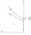
- FIG. 1is a graph illustrating the characteristic curves (optical power in mW vs. injection current in mA) (LI curves) associated with a given laser and the effect of temperature changes, age, internal parameters, and/or parasitics on the linearity of these curves (i.e. the non-linearity problem associated with analog optical transmission);
- FIG. 2is a schematic diagram illustrating one exemplary embodiment of the compact analog directly modulated laser configuration of the present invention, the compact analog directly modulated laser configuration incorporating a relatively large bandwidth photo-detector and negative feedback correction loop coupled to the back facet of the laser, providing high-gain, linear negative feedback to the input analog electrical signals; and
- FIG. 3is a schematic diagram illustrating one exemplary embodiment of the negative feedback correction loop of FIG. 2 .
- analog optical signalscan be generated using highly-linear directly modulated lasers, such as semiconductor lasers, laser diodes, and the like.
- the characteristic curves 10(optical power in mW vs. injection current in mA) (LI curves) of these lasers must be substantially linear and curve or “kink”-free above a threshold current 16 ( FIG. 1 ) (I s ) at which lasing begins.
- I sthreshold current
- analog optical signalscan be generated using externally modulated lasers to compensate, to some extent, for any non-linearity.
- the overall requirement, using either modulation schemeis that the generated analog optical signals closely match the input analog electrical signals, without significant distortion. In other words, slope variation compensation must be incorporated in order to maintain a relatively constant extinction ratio of the transmitted analog optical signals.
- Direct analog modulation (predistortion) techniquesinclude amplitude modulation (AM) techniques, quadrature amplitude modulation (QAM) techniques, frequency modulation (FM) techniques, intensity modulation (IM) techniques, and the like, well known to those of ordinary skill in the art. These direct analog modulation techniques are typically applied to Fabry-Perot (FP) and distributed feedback (DFB) cavity-design lasers and have the advantage of substantially smaller bandwidth requirements than digital modulation techniques, such as digital pulse code modulation techniques and the like.
- AMamplitude modulation
- QAMquadrature amplitude modulation
- FMfrequency modulation
- IMintensity modulation
- FPFabry-Perot
- DFBdistributed feedback
- MZIMach-Zehnder interferometric
- non-linearityis caused by, among other things, temperature changes, age, internal parameters, and parasitics.
- the directly modulated lasersmust be replaced regularly, likely as often as once every few months, as performance degradation occurs. Due to their relatively high cost, this becomes an expensive proposition.
- This problemis exacerbated by the fact that optical network elements are continually being deployed closer to end users. Thus, these optical network elements are being deployed in uncontrolled “field” environments.
- the only “outside-plant” rated componentsare transceiver-based components for digital communications, not analog communications.
- the externally modulated lasers that compensate, to some extent, for non-linearitysuffer from component complexity and are also relatively expensive.
- the present inventionprovides a compact analog directly modulated laser configuration that is suitable for use in the field that uses electrical feedback to compensate for non-linearity in real time, such that no matter how the LI curve changes, the electrical feedback compensates for non-linearity by amplifying a portion of the output analog optical signal and combining it with the input analog electrical signal using the standard control method of negative feedback.
- the gain of the feedback loopis relatively high, the overall transfer function of the system is primarily dependent on the feedback loop gain block, which is substantially linear. This is accomplished by incorporating a relatively large bandwidth photo-detector at the back facet of the laser that both monitors the output power of the system and provides a feedback signal to the linearization control circuit, as well as an amplifier.
- the amplified signal from the relatively large bandwidth photo-detectoris used to correct for various undesirable effects, such as non-linearity and relative intensity noise (RIN) of the laser.
- RINrelative intensity noise
- the signal from the relatively large bandwidth photo-detectoralso allows the laser to operate effectively close to threshold.
- a laserin general, includes a cavity disposed between a front facet and a back facet. These facets are mirrors that reflect photons in the cavity.
- An electrical sourceis used to create a population inversion in the cavity, thereby creating the spontaneous emission of photons. These photons reflect between the front facet and the back facet in the cavity and encounter excited atoms, thereby producing the stimulated emission of photons.
- the photons created by this stimulated emissionhave the same direction as the spontaneously emitted photons that created them, as well as the same phase and wavelength.
- the electrical source used to create the population inversion in the cavitycan be an analog signal that is used to modulate the resulting optical signal.
- Such direct modulationis relatively simple and inexpensive, as compared to external modulation.
- an external modulatoris used to modulate the light from a laser.
- external modulationprovides improved linearity performance and enhanced stability of the resulting optical signal, at the expense of component complexity and expense.
- the laser configuration 20 of the present inventionincludes a laser 22 , such as a semiconductor laser, laser diode (Fabry-Perot (FP), distributed feedback (DFB), or the like), etc., including a front facet 24 and a back facet 26 . These facets 24 , 26 are mirrors having a predetermined reflectivity based on the desired characteristics of the laser 22 .
- the optical output power of the laser 22is measured via a tap and optical splitter coupled to the front facet 24 of the laser 22 . This measurement approach has the disadvantage of significantly decreasing the optical output power of the laser 22 , as well as adding to component bulk.
- the optical output power of the laser 22is measured via a photo-detector 28 coupled to the back facet 26 of the laser 22 .
- the back facet 26 of the laser 22is a mirror with partial reflectivity. This partial reflectivity can be relatively small in degree, as the photo-detector 28 is disposed relatively close to the back facet 26 of the laser 22 .
- the laser diodeincludes a single-mode fiber pigtail, a heat sink, a thermo-electric (TE) cooler, a thermistor, and a monitor diode (photo-detector 28 ). The case is coupled to the laser chip via an anode and is grounded.
- the laser configuration 20 of the present inventionalso includes a feedback correction loop 30 coupled to the photo-detector 28 .
- the input analog electrical current 32 (I) of the laseris modulated, resulting in modulation analog electrical current 34 (I mod ), which is modified by feedback analog electrical current 36 (I f ).
- the laser transfer functionX
- the feedback correction loop transfer functionY
- the overall system transfer functionZ
- ZX/(1+XY)
- the feedback correction loop 30is a negative (180-degree inversion) feedback correction loop, although other suitable feedback correction loops can be used.
- the photo-detector assembly 38 , the feedback correction loop 30 , and the linearization control circuit 40include the photo-detector 28 and a resistor 42 , a transimpedance amplifier 44 (TIA) and a feedback resistor 46 (R f ), and a radio frequency (RF) combiner 48 and a resistor 50 (such as a 50 ohm resistor or the like), respectively.
- the photo-detector assembly 38disposed at the back facet 26 ( FIG. 2 ) of the laser 22 ( FIG.
- the feedback correction loop 30provide the feedback analog electrical current 36 (I f ) to the linearization control circuit 40 , where the feedback analog electrical current 36 (I f ) is combined with the input analog electrical current 32 (I) to form the modulation analog electrical current 34 (I mod ), which modulates the laser 22 .
- the output of the transimpedance amplifier 44 (TIA)is 180 degrees out-of-phase with the input.
- the back facet 26 of the laser 22incorporates a relatively large bandwidth photo-detector 28 that both monitors the optical output power of the system (as is done with conventional systems) and provides a feedback signal to the linearization control circuit 40 ( FIG. 3 ).
- a 2.5 GHz bandwidth photo-detector 28is used for the transmission of a 2.5 GHz analog optical signal
- a 10 GHz bandwidth photo-detector 28is used for the transmission of a 10 GHz analog optical signal, etc.
- the photodiode specification(and the specification of each system component, including the laser 22 ) is carefully selected such that it coincides with the desired rate (signal frequency).
- Relative intensity noise (RIN) of the laseris reduced using the systems and methods (and the feedback correction loop) of the present invention as demonstrated by experimental measurement of the signal-to-noise ratio (SNR) at a given laser output power with and without the feedback correction loop present.
Landscapes
- Physics & Mathematics (AREA)
- Condensed Matter Physics & Semiconductors (AREA)
- General Physics & Mathematics (AREA)
- Electromagnetism (AREA)
- Optics & Photonics (AREA)
- Semiconductor Lasers (AREA)
Abstract
Description
- Compensation of the slope variation of a laser diode due to temperature and/or time is thus achieved without the use of low frequency ripple or peak detection, rather the a.c. and mean optical powers are compared in order to obtain the optimum optical extinction ratio. The a.c. optical signal power is used to indicate a reduction in slope efficiency.
- The description above refers to laser diodes for use in optical fibre transmission systems. There is, however, growing interest in optical microwave subcarrier communications and transmitters therefore, which would also employ laser diodes and require slope variation compensation. The arrangement described above with reference to
FIG. 1 is not suitable for such microwave applications without modification. This is due to the limited bandwidth of theback facet photodiode 12 and the problem is enhanced as the bit rate increases. If the overall optical transmitter were to be employed as an analogue transmitter where a small microwave signal was modulated on the linear portion of the laser diode characteristic, a conventional back facet photodiode would not be usable. - However, a fibre
optical coupler 30 can be arranged at the laser diode output as indicated inFIG. 3 so as to split off a small proportion of the output signal and apply it to a very high frequencymicrowave PIN photodiode 32, for example a 30 GHz device, and the slope may be very accurately compensated as a result. The remainder of the laser diode optical output is available from thecoupler 30 atoutput 34. The output ofPIN photodiode 32 is applied to two loops as before. The d.c. information is applied toloop 1 including alow pass filter 34 and compared with a reference voltage Vr1 used to set the d.c. (mean power) operating point. The resultant error signal ΔV1 is applied to atransconductance amplifier 36 to produce bias current Ib′ which is low pass filtered at38 and the resultant bias current Ib applied to thelaser diode 10.
Claims (25)
Priority Applications (1)
| Application Number | Priority Date | Filing Date | Title |
|---|---|---|---|
| US11/398,107US7505496B2 (en) | 2006-04-05 | 2006-04-05 | Systems and methods for real-time compensation for non-linearity in optical sources for analog signal transmission |
Applications Claiming Priority (1)
| Application Number | Priority Date | Filing Date | Title |
|---|---|---|---|
| US11/398,107US7505496B2 (en) | 2006-04-05 | 2006-04-05 | Systems and methods for real-time compensation for non-linearity in optical sources for analog signal transmission |
Publications (2)
| Publication Number | Publication Date |
|---|---|
| US20070237194A1 US20070237194A1 (en) | 2007-10-11 |
| US7505496B2true US7505496B2 (en) | 2009-03-17 |
Family
ID=38575193
Family Applications (1)
| Application Number | Title | Priority Date | Filing Date |
|---|---|---|---|
| US11/398,107ActiveUS7505496B2 (en) | 2006-04-05 | 2006-04-05 | Systems and methods for real-time compensation for non-linearity in optical sources for analog signal transmission |
Country Status (1)
| Country | Link |
|---|---|
| US (1) | US7505496B2 (en) |
Cited By (1)
| Publication number | Priority date | Publication date | Assignee | Title |
|---|---|---|---|---|
| CN110911948A (en)* | 2019-11-29 | 2020-03-24 | 西安奇芯光电科技有限公司 | Chirp management laser based on hybrid integration technology |
Families Citing this family (7)
| Publication number | Priority date | Publication date | Assignee | Title |
|---|---|---|---|---|
| US8085824B2 (en)* | 2007-05-31 | 2011-12-27 | Finisar Corporation | Optimization of laser parameters to achieve desired performance |
| JP5350940B2 (en)* | 2009-08-19 | 2013-11-27 | 浜松ホトニクス株式会社 | Laser module |
| WO2011146363A2 (en)* | 2010-05-17 | 2011-11-24 | Neophotonics Corporation | Hybrid fiber coaxial network optical transport system with distortion control |
| US8849129B2 (en)* | 2012-07-20 | 2014-09-30 | Finisar Corporation | Method and apparatus for stabilization of optical transmitter |
| US9553679B2 (en)* | 2013-07-24 | 2017-01-24 | Bae Systems Information And Electronic Systems Integrations Inc. | Analog radio frequency memory for signal replication |
| CN106998230B (en) | 2017-03-07 | 2019-07-09 | 武汉光迅科技股份有限公司 | Dual rate DML device, module and the signal calibration method of built-in signal calibration circuit |
| CN116264481A (en)* | 2021-12-14 | 2023-06-16 | 华为技术有限公司 | A communication device and method |
Citations (41)
| Publication number | Priority date | Publication date | Assignee | Title |
|---|---|---|---|---|
| US4873690A (en) | 1986-12-15 | 1989-10-10 | British Telecommunications Public Limited Company | Optical switch |
| US4924470A (en) | 1989-07-25 | 1990-05-08 | Gordon Ries | Laser diode control apparatus |
| US5012484A (en) | 1990-01-02 | 1991-04-30 | At&T Bell Laboratories | Analog optical fiber communication system, and laser adapted for use in such a system |
| US5111475A (en) | 1990-01-02 | 1992-05-05 | At&T Bell Laboratories | Analog optical fiber communication system, and laser adapted for use in such a system |
| US5208824A (en) | 1991-12-12 | 1993-05-04 | At&T Bell Laboratories | Article comprising a DFB semiconductor laser |
| US5252839A (en) | 1992-06-10 | 1993-10-12 | Hewlett-Packard Company | Superluminescent light-emitting diode with reverse biased absorber |
| US5285468A (en) | 1992-07-17 | 1994-02-08 | At&T Bell Laboratories | Analog optical fiber communication system, and laser adapted for use in such a system |
| US5311005A (en) | 1991-10-19 | 1994-05-10 | Northern Telecom Limited | Optical transmitters |
| US5321710A (en) | 1993-04-19 | 1994-06-14 | Raynet Corporation | Predistortion method and apparatus for laser linearization |
| US5579328A (en) | 1995-08-10 | 1996-11-26 | Northern Telecom Limited | Digital control of laser diode power levels |
| US5600126A (en) | 1995-06-20 | 1997-02-04 | Xerox Corporation | Method and apparatus for controlling the power output of multiple laser diodes |
| US5642375A (en) | 1995-10-26 | 1997-06-24 | Hewlett-Packard Company | Passively-locked external optical cavity |
| US5657124A (en)* | 1994-02-18 | 1997-08-12 | Saint Gobain Cinematique Et Controle | Method of measuring the thickness of a transparent material |
| US5659414A (en) | 1995-06-20 | 1997-08-19 | Xerox Corporation | Means for controlling the power output of laser diodes in a ROS system |
| US5684623A (en) | 1996-03-20 | 1997-11-04 | Hewlett Packard Company | Narrow-band tunable optical source |
| US5724088A (en) | 1996-03-27 | 1998-03-03 | Xerox Corporation | High-speed, reflex-controlled laser circuit for an electrophotographic printer |
| US5835121A (en) | 1995-04-21 | 1998-11-10 | Xerox Corporation | Pixel exposure control for a raster output scanner in an electrophotographic printer |
| US5835522A (en) | 1996-11-19 | 1998-11-10 | Hewlett-Packard Co. | Robust passively-locked optical cavity system |
| US5956355A (en) | 1991-04-29 | 1999-09-21 | Massachusetts Institute Of Technology | Method and apparatus for performing optical measurements using a rapidly frequency-tuned laser |
| US5963570A (en)* | 1997-05-12 | 1999-10-05 | At&T Corp. | Current control for an analog optical link |
| US6124956A (en) | 1997-12-04 | 2000-09-26 | Nortel Networks Limited | Optical transmitter output monitoring tap |
| US6192058B1 (en) | 1998-09-18 | 2001-02-20 | Sarnoff Corporation | Multiwavelength actively mode-locked external cavity semiconductor laser |
| US6347107B1 (en) | 1998-07-15 | 2002-02-12 | Eastman Kodak Company | System and method of improving intensity control of laser diodes using back facet photodiode |
| US6351310B1 (en) | 1996-04-19 | 2002-02-26 | Kvh Industries, Inc. | Reduced minimum configuration interferometric fiber optic gyroscope with simplified signal processing electronics |
| US6370175B1 (en)* | 1998-04-13 | 2002-04-09 | Fuji Xerox Co., Ltd. | Laser beam luminous energy correction method, laser driving apparatus, laser beam scanner and image recording device |
| US20030090289A1 (en)* | 2001-11-13 | 2003-05-15 | Sean Morley | Method and circuit for measuring the optical modulation amplitude (OMA) in the operating region of a laser diode |
| US6597485B1 (en)* | 1999-03-19 | 2003-07-22 | Fujitsu Limited | Optical transmitter circuit |
| US6609842B1 (en)* | 2000-03-27 | 2003-08-26 | Marconi Communications, Inc. | Linear laser driver circuit |
| US20030193977A1 (en)* | 2002-04-12 | 2003-10-16 | Chia-Ming Tsai | Light-emitting device driving circuit |
| US6647046B1 (en) | 1999-11-23 | 2003-11-11 | Corning Lasertron, Inc. | Mode-selective facet layer for pump laser |
| US20040022284A1 (en)* | 2002-07-30 | 2004-02-05 | Broadcom Corporation | Jitter suppression techniques for laser driver circuits |
| US6724793B2 (en)* | 2001-06-19 | 2004-04-20 | Sony Corporation | Laser diode drive circuit and amplifying circuit for optical disc recording and/or reproducing apparatus |
| US6778570B2 (en)* | 2001-05-07 | 2004-08-17 | Sony Corporation | Laser driving apparatus and method |
| US6865199B2 (en) | 2001-07-27 | 2005-03-08 | General Instrument Corporation | Inexpensive analog laser module |
| US6917639B2 (en)* | 2001-08-09 | 2005-07-12 | Ricoh Company, Ltd. | Laser driver circuit |
| US6928094B2 (en)* | 2002-12-16 | 2005-08-09 | Intel Corporation | Laser driver circuit and system |
| US6937780B2 (en) | 2000-02-25 | 2005-08-30 | Trumpf Photonics, Inc. | Multi-pass, arcuate bent waveguide, high power super luminescent diode |
| US6950452B2 (en) | 2001-09-28 | 2005-09-27 | The Furukawa Electric Co., Ltd. | Semiconductor laser module and method for simultaneously reducing relative intensity noise (RIN) and stimulated brillouin scattering (SBS) |
| US20050271396A1 (en) | 2004-03-19 | 2005-12-08 | John Iannelli | Directly modulated laser optical transmission system |
| US20050271100A1 (en)* | 2004-06-04 | 2005-12-08 | Keith Everett | System and method for controlling optical sources, such as laser diodes, and computer program product therefor |
| US7085296B2 (en)* | 2003-12-05 | 2006-08-01 | Branson Ultrasonics Corporation | Dual parameter laser optical feedback |
- 2006
- 2006-04-05USUS11/398,107patent/US7505496B2/enactiveActive
Patent Citations (43)
| Publication number | Priority date | Publication date | Assignee | Title |
|---|---|---|---|---|
| US4873690A (en) | 1986-12-15 | 1989-10-10 | British Telecommunications Public Limited Company | Optical switch |
| US4924470A (en) | 1989-07-25 | 1990-05-08 | Gordon Ries | Laser diode control apparatus |
| US5012484A (en) | 1990-01-02 | 1991-04-30 | At&T Bell Laboratories | Analog optical fiber communication system, and laser adapted for use in such a system |
| US5111475A (en) | 1990-01-02 | 1992-05-05 | At&T Bell Laboratories | Analog optical fiber communication system, and laser adapted for use in such a system |
| US6160826A (en) | 1991-04-29 | 2000-12-12 | Massachusetts Institute Of Technology | Method and apparatus for performing optical frequency domain reflectometry |
| US5956355A (en) | 1991-04-29 | 1999-09-21 | Massachusetts Institute Of Technology | Method and apparatus for performing optical measurements using a rapidly frequency-tuned laser |
| US5311005A (en) | 1991-10-19 | 1994-05-10 | Northern Telecom Limited | Optical transmitters |
| US5208824A (en) | 1991-12-12 | 1993-05-04 | At&T Bell Laboratories | Article comprising a DFB semiconductor laser |
| US5252839A (en) | 1992-06-10 | 1993-10-12 | Hewlett-Packard Company | Superluminescent light-emitting diode with reverse biased absorber |
| US5285468A (en) | 1992-07-17 | 1994-02-08 | At&T Bell Laboratories | Analog optical fiber communication system, and laser adapted for use in such a system |
| US5321710A (en) | 1993-04-19 | 1994-06-14 | Raynet Corporation | Predistortion method and apparatus for laser linearization |
| US5657124A (en)* | 1994-02-18 | 1997-08-12 | Saint Gobain Cinematique Et Controle | Method of measuring the thickness of a transparent material |
| US5835121A (en) | 1995-04-21 | 1998-11-10 | Xerox Corporation | Pixel exposure control for a raster output scanner in an electrophotographic printer |
| US5600126A (en) | 1995-06-20 | 1997-02-04 | Xerox Corporation | Method and apparatus for controlling the power output of multiple laser diodes |
| US5659414A (en) | 1995-06-20 | 1997-08-19 | Xerox Corporation | Means for controlling the power output of laser diodes in a ROS system |
| US5579328A (en) | 1995-08-10 | 1996-11-26 | Northern Telecom Limited | Digital control of laser diode power levels |
| US5642375A (en) | 1995-10-26 | 1997-06-24 | Hewlett-Packard Company | Passively-locked external optical cavity |
| US5684623A (en) | 1996-03-20 | 1997-11-04 | Hewlett Packard Company | Narrow-band tunable optical source |
| US5724088A (en) | 1996-03-27 | 1998-03-03 | Xerox Corporation | High-speed, reflex-controlled laser circuit for an electrophotographic printer |
| US6351310B1 (en) | 1996-04-19 | 2002-02-26 | Kvh Industries, Inc. | Reduced minimum configuration interferometric fiber optic gyroscope with simplified signal processing electronics |
| US5835522A (en) | 1996-11-19 | 1998-11-10 | Hewlett-Packard Co. | Robust passively-locked optical cavity system |
| US5963570A (en)* | 1997-05-12 | 1999-10-05 | At&T Corp. | Current control for an analog optical link |
| US6124956A (en) | 1997-12-04 | 2000-09-26 | Nortel Networks Limited | Optical transmitter output monitoring tap |
| US6370175B1 (en)* | 1998-04-13 | 2002-04-09 | Fuji Xerox Co., Ltd. | Laser beam luminous energy correction method, laser driving apparatus, laser beam scanner and image recording device |
| US6347107B1 (en) | 1998-07-15 | 2002-02-12 | Eastman Kodak Company | System and method of improving intensity control of laser diodes using back facet photodiode |
| US6192058B1 (en) | 1998-09-18 | 2001-02-20 | Sarnoff Corporation | Multiwavelength actively mode-locked external cavity semiconductor laser |
| US6597485B1 (en)* | 1999-03-19 | 2003-07-22 | Fujitsu Limited | Optical transmitter circuit |
| US6647046B1 (en) | 1999-11-23 | 2003-11-11 | Corning Lasertron, Inc. | Mode-selective facet layer for pump laser |
| US6937780B2 (en) | 2000-02-25 | 2005-08-30 | Trumpf Photonics, Inc. | Multi-pass, arcuate bent waveguide, high power super luminescent diode |
| US6609842B1 (en)* | 2000-03-27 | 2003-08-26 | Marconi Communications, Inc. | Linear laser driver circuit |
| US6778570B2 (en)* | 2001-05-07 | 2004-08-17 | Sony Corporation | Laser driving apparatus and method |
| US6724793B2 (en)* | 2001-06-19 | 2004-04-20 | Sony Corporation | Laser diode drive circuit and amplifying circuit for optical disc recording and/or reproducing apparatus |
| US6865199B2 (en) | 2001-07-27 | 2005-03-08 | General Instrument Corporation | Inexpensive analog laser module |
| US6917639B2 (en)* | 2001-08-09 | 2005-07-12 | Ricoh Company, Ltd. | Laser driver circuit |
| US6950452B2 (en) | 2001-09-28 | 2005-09-27 | The Furukawa Electric Co., Ltd. | Semiconductor laser module and method for simultaneously reducing relative intensity noise (RIN) and stimulated brillouin scattering (SBS) |
| US6907055B2 (en)* | 2001-11-13 | 2005-06-14 | Analog Devices, Inc. | Method and circuit for measuring the optical modulation amplitude (OMA) in the operating region of a laser diode |
| US20030090289A1 (en)* | 2001-11-13 | 2003-05-15 | Sean Morley | Method and circuit for measuring the optical modulation amplitude (OMA) in the operating region of a laser diode |
| US20030193977A1 (en)* | 2002-04-12 | 2003-10-16 | Chia-Ming Tsai | Light-emitting device driving circuit |
| US20040022284A1 (en)* | 2002-07-30 | 2004-02-05 | Broadcom Corporation | Jitter suppression techniques for laser driver circuits |
| US6928094B2 (en)* | 2002-12-16 | 2005-08-09 | Intel Corporation | Laser driver circuit and system |
| US7085296B2 (en)* | 2003-12-05 | 2006-08-01 | Branson Ultrasonics Corporation | Dual parameter laser optical feedback |
| US20050271396A1 (en) | 2004-03-19 | 2005-12-08 | John Iannelli | Directly modulated laser optical transmission system |
| US20050271100A1 (en)* | 2004-06-04 | 2005-12-08 | Keith Everett | System and method for controlling optical sources, such as laser diodes, and computer program product therefor |
Non-Patent Citations (6)
| Title |
|---|
| Charles Cox III, Edward Ackerman, Roger Helkey, Gary E. Betts; IEEE Transactions On Microwave Theory and Techniques, vol. 45, No. 8, Aug. 1997; "Techniques and Performance of Intensity-Modulation Direct-Detection Analog Optical Links"; Lexington, MA. |
| Ram Sadwani, and Bahram Jalal with IEEE; Journal Of Lightwave Technology vol. 21, No. 12, Dec. 2003; "Adaptive CMOS Predistortion Linearizer for Fiber-Optic Links". |
| Satheesan Nadarajah, Xavier N. Fernando, Rexa Sedaghat; CCECE 2003-CCGEI 2003, "Adaptive Digital Predistortion of Laser Diode Nonlinearity For Wireless Applications"; Department of Electrical and Electtronic Engineering, Ryerson University; Montreal. |
| T. Ismail, C. P. Liu and A. J. Seeds; "Uncooled directly modulated high dynamic range source for IEEE802.11a wireless over fibre LAN applications": Proceedings of the Optical Fiber Conference (OFC), 2004, FE3. |
| Y. Chiu, B. Jalali, S. Garner, and W. Steier.; IEEE Photonics Technology Letters, vol. 11, No. 1, Jan. 1999; "Broad-Band Electronic Linearizer for Externally Modulated Analog Fiber-Optic Links". |
| Y. Chiu, B. Jalali, S. Garner, and W. Steier; "Broad-Band Electronic Linearizer for Externally Modulated Analog Fiber-Optic Links"; IEEE Photonics Technology Letters, vol. 11, No. 1, Jan. 1999; (c) 1999 IEEE. Los Angeles, CA. |
Cited By (1)
| Publication number | Priority date | Publication date | Assignee | Title |
|---|---|---|---|---|
| CN110911948A (en)* | 2019-11-29 | 2020-03-24 | 西安奇芯光电科技有限公司 | Chirp management laser based on hybrid integration technology |
Also Published As
| Publication number | Publication date |
|---|---|
| US20070237194A1 (en) | 2007-10-11 |
Similar Documents
| Publication | Publication Date | Title |
|---|---|---|
| US7505496B2 (en) | Systems and methods for real-time compensation for non-linearity in optical sources for analog signal transmission | |
| EP0503579B1 (en) | Broad linewidth lasers for optical fiber communication systems | |
| US9564734B2 (en) | Method of fabricating and operating an optical modulator | |
| US5295209A (en) | Spontaneous emission source having high spectral density at a desired wavelength | |
| EP0415645B1 (en) | Interferometric devices for reducing harmonic distortions in laser communication systems | |
| KR101523396B1 (en) | Method and apparatus for a low-chirp transmitter for fiber optic communications | |
| US9438007B2 (en) | Optical modulator | |
| HK1011158B (en) | Broad linewidth lasers for optical fiber communication systems | |
| CN1312866C (en) | Optical Linearizers for Fiber Optic Communications | |
| US20090290613A1 (en) | External cavity laser assembly including external chirped exit reflector for improved linearity | |
| US7778552B2 (en) | Directly modulated laser with integrated optical filter | |
| US4755016A (en) | Coherent lightwave transmitters | |
| US7620081B2 (en) | Semiconductor laser utilizing real-time linewidth reduction method | |
| US6738187B2 (en) | Semiconductor optical amplifiers using wavelength locked loop tuning and equalization | |
| Atra et al. | O-band reflective electroabsorption modulator for 50 Gb/s NRZ and PAM-4 colorless transmission | |
| JP2002299751A (en) | Semiconductor laser device and optical transmission device using the same. | |
| Ackerman et al. | Telecommunication lasers | |
| CN112993753B (en) | Monolithic integrated waveguide device and integrated semiconductor chip thereof | |
| Adams et al. | 1.55 µm transmission at 2.5 Gbit/s over 1102 km of NDSF using discrete and monolithically integrated InGaAsP/InP Mach-Zehnder modulator and DFB laser | |
| SATO et al. | Semiconductor Optical Amplifier and Gain Chip Used in Wavelength Tunable Lasers | |
| Nakajima et al. | Generation of 10-Gbit/s optical millimeter-wave signal using a 125-GHz mode-locked laser diode integrated with an electro-absorption modulator | |
| CA2202304C (en) | Broadwidth linewidth lasers for optical fiber communication systems | |
| Williams et al. | Acknowledgments: The authors are pleased to acknowledge the support and assistance given by a number of colleagues, especially NW Forbes, N. Cam and AK Wood. Grateful acknowledgment is also made to the EC, ACTS BLISS programme AC06S which supported this work. | |
| US20030193706A1 (en) | System and method for minimizing interferometric distortion in directly modulated analog fiber optic links | |
| Jung et al. | Suppression of chromatic dispersion effects using SOA in analog optical transmission link |
Legal Events
| Date | Code | Title | Description |
|---|---|---|---|
| AS | Assignment | Owner name:CIENA CORPORATION, MARYLAND Free format text:ASSIGNMENT OF ASSIGNORS INTEREST;ASSIGNOR:SHAHINE, M. H.;REEL/FRAME:017767/0665 Effective date:20060331 | |
| FEPP | Fee payment procedure | Free format text:PAYOR NUMBER ASSIGNED (ORIGINAL EVENT CODE: ASPN); ENTITY STATUS OF PATENT OWNER: LARGE ENTITY | |
| STCF | Information on status: patent grant | Free format text:PATENTED CASE | |
| FPAY | Fee payment | Year of fee payment:4 | |
| AS | Assignment | Owner name:DEUTSCHE BANK AG NEW YORK BRANCH, NEW YORK Free format text:SECURITY INTEREST;ASSIGNOR:CIENA CORPORATION;REEL/FRAME:033329/0417 Effective date:20140715 | |
| AS | Assignment | Owner name:BANK OF AMERICA, N.A., AS ADMINISTRATIVE AGENT, NO Free format text:PATENT SECURITY AGREEMENT;ASSIGNOR:CIENA CORPORATION;REEL/FRAME:033347/0260 Effective date:20140715 | |
| FPAY | Fee payment | Year of fee payment:8 | |
| FEPP | Fee payment procedure | Free format text:PAYER NUMBER DE-ASSIGNED (ORIGINAL EVENT CODE: RMPN); ENTITY STATUS OF PATENT OWNER: LARGE ENTITY Free format text:PAYOR NUMBER ASSIGNED (ORIGINAL EVENT CODE: ASPN); ENTITY STATUS OF PATENT OWNER: LARGE ENTITY | |
| AS | Assignment | Owner name:CIENA CORPORATION, MARYLAND Free format text:RELEASE BY SECURED PARTY;ASSIGNOR:DEUTSCHE BANK AG NEW YORK BRANCH;REEL/FRAME:050938/0389 Effective date:20191028 | |
| AS | Assignment | Owner name:BANK OF AMERICA, N.A., AS COLLATERAL AGENT, ILLINO Free format text:PATENT SECURITY AGREEMENT;ASSIGNOR:CIENA CORPORATION;REEL/FRAME:050969/0001 Effective date:20191028 | |
| MAFP | Maintenance fee payment | Free format text:PAYMENT OF MAINTENANCE FEE, 12TH YEAR, LARGE ENTITY (ORIGINAL EVENT CODE: M1553); ENTITY STATUS OF PATENT OWNER: LARGE ENTITY Year of fee payment:12 | |
| AS | Assignment | Owner name:CIENA CORPORATION, MARYLAND Free format text:RELEASE BY SECURED PARTY;ASSIGNOR:BANK OF AMERICA, N.A.;REEL/FRAME:065630/0232 Effective date:20231024 |