US7503026B2 - Cell, standard cell, standard cell library, a placement method using standard cell, and a semiconductor integrated circuit - Google Patents
Cell, standard cell, standard cell library, a placement method using standard cell, and a semiconductor integrated circuitDownload PDFInfo
- Publication number
- US7503026B2 US7503026B2US11/305,191US30519105AUS7503026B2US 7503026 B2US7503026 B2US 7503026B2US 30519105 AUS30519105 AUS 30519105AUS 7503026 B2US7503026 B2US 7503026B2
- Authority
- US
- United States
- Prior art keywords
- cell
- routing
- along
- wiring
- standard cell
- Prior art date
- Legal status (The legal status is an assumption and is not a legal conclusion. Google has not performed a legal analysis and makes no representation as to the accuracy of the status listed.)
- Active, expires
Links
Images


Classifications
- G—PHYSICS
- G06—COMPUTING OR CALCULATING; COUNTING
- G06F—ELECTRIC DIGITAL DATA PROCESSING
- G06F30/00—Computer-aided design [CAD]
- G06F30/30—Circuit design
- G06F30/39—Circuit design at the physical level
- G06F30/392—Floor-planning or layout, e.g. partitioning or placement
- H—ELECTRICITY
- H10—SEMICONDUCTOR DEVICES; ELECTRIC SOLID-STATE DEVICES NOT OTHERWISE PROVIDED FOR
- H10D—INORGANIC ELECTRIC SEMICONDUCTOR DEVICES
- H10D84/00—Integrated devices formed in or on semiconductor substrates that comprise only semiconducting layers, e.g. on Si wafers or on GaAs-on-Si wafers
- H10D84/90—Masterslice integrated circuits
- H10D84/903—Masterslice integrated circuits comprising field effect technology
- H10D84/907—CMOS gate arrays
Definitions
- the present inventionrelates to a standard cell, a standard cell library and a placement method of standard cells for higher integration and area reduction.
- terminals of a cell for the communication of input/output signalsmust be located at the intersections of routing grids in the X and Y directions.
- the X directiondenotes a direction along a power-supply routing of a standard cell
- the Y directiondenotes a direction vertical to the power-supply routing.
- the height and the width of the cellare respectively set to an integral multiple of the interval between the routing grids so that the terminals can always locate at the grid intersection when the cells are placed adjacently with no spacing therebetween.
- the automatic placement & routing tooldecide the location of the cells so that their terminals are located at the grid intersection. Then, the automatic placement & routing tool determines the position at which the cell is placed so that the position of the terminal is located at the routing grid intersection.
- FIG. 17is a layout of a standard cell according to a conventional technology.
- C 41 , C 42 and C 43denote a standard cell
- Tdenotes a terminal capable of communicating an input signal or an output signal in the standard cell
- Gdenotes a gate electrode.
- the gate electrode Gextends in the Y direction because the power-supply wiring is provided in the X direction.
- FIG. 17shows that the terminals T cannot locate at the grid intersection when a cell width Lc along the X direction is not an integral multiple of a routing grid interval Lx in the X direction.
- None of the widths of the cells C 41 , C 42 and C 43 disposed on the upper side in FIG. 17is the integral multiple of the routing grid interval Lx in the X direction.
- the cells C 41 , C 42 and C 43are identical in order to simplify the description.
- the terminals T of the cells C 41 and C 43locate at the grid intersection, while the terminals T of the cell C 42 do not. In other words, the terminals T of the cell C 42 fail to be connected in the automatic placement & routing design.
- regions R 1 , R 2 and R 3are provided to adjust the cell width to the integral multiple of the routing grid interval in the same manner as cells C 51 , C 52 and C 53 disposed on the lower side in FIG.
- origins O 51 , O 52 and O 53 of the cells C 51 , C 52 and C 53locate at midpoints between the routing grids adjacent to one another along both of the X and Y directions. Accordingly, all of the terminals T can locate at the grid intersection.
- the regions R 1 , R 2 and R 3which are only provided exclusively for the adjustment in the conventional technology, are normally unnecessary and do not include any device required for a circuit such as a transistor and wiring. As a result, a cell area increases, which is one of the factors obstructing the area reduction of LSI.
- each cellis placed based on the routing grid in performing the automatic placement in the automatic placement & routing tool with the on-grid design scheme. Therefore, when the cell width is not the integral multiple of the routing grid as in the cells C 41 , C 42 and C 43 shown on the upper side in FIG. 17 , the cells cannot be placed adjacently with no spacing therebetween as shown on the upper side in FIG. 17 . In the automatic placement, the cells are actually placed as shown on the lower side in FIG. 17 . Because the cells C 41 , C 42 and C 43 are identical in the example shown in FIG. 17 , it may be possible to use the widths of the cells C 41 , C 42 and C 43 as placement grid in the automatic placement and place the cells shown on the upper side in FIG. 17 in the automatic placement based on the placement grids. However, the automatic placement in the foregoing manner cannot be applied when a plurality of cells to be placed include non-identical cells and are designed so that their widths are arbitrary.
- a precision in a finished dimension of the gate electrode ultimately obtainedis deteriorated by an optical proximity effect when an interval between the gate electrodes and gate lengths of the gate electrodes are irregular in their patterns.
- performances of respective transistors of the semiconductor integrated circuitare increasingly inconstant, which leads to an increased variation in a performance of the semiconductor integrate circuit. As a result, a yield ratio is decreased.
- FIG. 18shows a result of the application of the foregoing conventional technology to the standard cell shown in FIG. 17 .
- Dummy gate electrodes DGare provided on cell boundaries of standard cells C 41 ′, C 41 ′ and C 43 ′ disposed on the upper side in FIG. 18 . These dummy gate electrodes DG are shared between the adjacent standard cells.
- the gate electrodes G and the dummy gate electrodes DGare respectively equally spaced, and their gate their lengths are equal. Accordingly, the gate electrode pattern, gate length and gate interval (in particular, gate electrode pattern) are regular, not only inside the cell, but also between the cells.
- the pattern of the gate electrode, gate length and gate intervalare regular not only inside each of the cells but also between the cells. As a result, the precision in the finished dimension of the gate electrode can be improved.
- the OPCcan be processed in each standard cell.
- the OPCcan be processed in each of the standard cells C 41 , C 42 and C 43 disposed on the upper side in FIG. 17 where the dummy gate electrodes DG are not provided because a distance from the cell boundary of each standard cell to the gate electrode in the closest vicinity and a distance from the cell boundary of an adjacent standard cell to the gate electrode in the closest vicinity can be constant when the distance from the cell boundary of each standard cell to the gate electrode in the closest vicinity is constant.
- the gate electrode located on the cell boundary of the standard cellcannot be shared.
- the dummy electrodes DGare located with less than a minimum interval allowed in a design rule therebetween, which results in an error in the design rule.
- it is necessary to enlarge the gate lengthfor example, in the same manner as the dummy gate DG 2 disposed on the lower side in FIG. 18 .
- the gate interval in each standard cellcan be maintained at the constant level when such the gate length enlargement is executed, the gate length becomes irregular at the dummy gate electrodes DG 2 , which results in the imprecision of the finished dimension of the gate electrodes. Further, the OPC cannot be processed in each standard cell due to the different gate lengths in the dummy gate electrodes DG in each standard cell and the dummy gate electrodes DG 2 adjacent thereto. As a result, the OPC has to be processed with respect to the entire semiconductor integrated circuit.
- the regions R 1 , R 2 and R 3are provided, there is an disadvantage even in the standard cells C 51 , C 52 and C 53 disposed on the lower side in FIG. 17 without the dummy gate electrodes DG and DG 2 though the distance from the cell boundary of each standard cell to the gate electrode in the closest vicinity in the cell is made constant.
- the cell boundary positionis changed when the regions R 1 , R 2 and R 3 are provided. In that case, though the distance from the cell boundary of each standard cell to the gate electrode in the closest vicinity in the cell is made constant, the distance from the cell boundary to the gate electrode in the closest vicinity becomes inconstant. As a result, the OPC cannot be processed in each standard cell.
- a main object of the present inventionis to provide a semiconductor integrated circuit capable of reducing a cell area and a chip area.
- Another main object of the present inventionis to provide a semiconductor integrated circuit capable of improving a precision in a finished dimension of a gate electrode despite a process miniaturization and processing the OPC in each standard cell.
- a standard cellis a cell comprising a plurality of terminals capable of transmitting an input signal or an output signal and serving as a minimum unit in designing the semiconductor integrated circuit, wherein the plurality of terminals is located on routing grids lined in a Y direction which is a direction vertical to a power-supply wiring of the cell used in automatic placement & routing and has a shape extended along an X direction which is a direction in parallel with the power-supply wiring.
- the shorter-side dimension of the terminalcorresponds to the wiring width in the automatic placement & routing
- the longer-side dimension of the terminalis at least “the routing grid interval along the X direction+the wiring width” and at most the length obtained by subtracting the minimum wiring interval from the cell width of the cell along the X direction.
- the shorter-side dimension of the terminalcorresponds to the wiring width in the automatic placement & routing
- the longer-side dimension of the terminalis equal to “the routing grid interval along the X direction+the wiring width”.
- a preferred embodiment 1 of the present inventionwhich will be described later, can be referenced to describe the foregoing constitutions of the present invention.
- the terminalwhen a Y coordinate of a cell origin is located at a routing grid midpoint, the terminal can be located at not less than one grid intersection regardless of an X coordinate of the cell origin. In other words, it becomes unnecessary for the X coordinate of each cell origin to be at the routing grid midpoint in the X direction. Accordingly, it becomes unnecessary to provide any additional region in the cell in order to locate all of the terminals on the routing grids or to generate any useless region between the cells. As a result, the chip area can be reduced.
- the dimension of the terminalmay correspond to the wiring width in the automatic placement & routing in its shorter-side dimension, and the longer-side dimension thereof maybe obtained by subtracting the minimum wring interval from the cell width of the standard cell along the X direction.
- a standard cell placement methodcomprises a step of placing the standard cell, a step of providing a tentative routing for the placed standard cell in accordance with a connection information, and a step of removing any part unnecessary for the wirings from the layout of the terminals included in the standard cell.
- a preferred embodiment 4 of the present inventionwhich will be described later, can be referenced to describe the constitution.
- the chip areacan be reduced.
- a routing resourceis increased as a result of the area reduction of the terminals, and the increased routing resource can be maximally utilized in the routing process between the standard cells. Therefore, an entire wiring length can be reduced, as a result of which the reduction of a wiring capacitance, the reduction of a delay time, and the reduction of a design TAT (turn around time) because of the increased routing resource can be expected.
- a standard cell library for synthesizing a functional macro layoutincludes a standard cell having a cell width different to an integral multiple of the routing grid interval.
- a preferred embodiment 2 of the present invention, which will be described later,can be referenced to describe the constitution.
- the X coordinate of the cell origin in the cell placementit becomes unnecessary for the X coordinate of the cell origin in the cell placement to be on the routing grid or at the midpoint between the adjacent routing grids, which allows the standard cells having a minimum size to be placed without any interval therebetween. As a result, an area of a logic part can be reduced.
- a standard cell placement methodis a design method for synthesizing a functional macro layout using the standard cell, wherein a Y coordinate of a cell origin of at least a standard cell is set to a midpoint between the adjacent routing grids or on the routing grid in the automatic placement & routing, and an X coordinate of the cell origin of the standard cell is set to the midpoint between the adjacent routing grids or to a position not on the routing grid.
- the standard cell used in the foregoing constitutioncan employ any of the standard cells described earlier.
- the preferred embodiments 1-4, which will be described later,can be referenced to describe the standard cell.
- the X coordinate of the cell originmay not necessarily be on the routing grid or at the midpoint between the adjacent routing grids, which allows the standard cells having a minimum size to be placed without any interval therebetween. As a result, the area of the logic part can be reduced.
- a standard cell placement methodis a design method for synthesizing a functional macro layout using the standard cell, wherein the standard cell is tentatively placed, and when a Y coordinate of a cell origin of the tentatively placed standard cell is located at a midpoint between the adjacent routing grids or on the routing grid in the automatic placement & routing and an X coordinate of the cell origin is located at the midpoint between the adjacent routing grids or on the routing grid, the cell origin is moved to a position where the standard cell having the cell origin is in contact with the adjacent standard cell.
- the standard cell used in the foregoing constitutioncan employ any of the standard cells described earlier.
- the preferred embodiment 3, which will be described later,can be referenced to describe the standard cell.
- a standard cell placement methodis a design method for synthesizing a functional macro layout using the standard cell, wherein the standard cell is tentatively placed, and, in the case where the tentatively placed standard cell includes a first group of cells each having a cell width corresponding to an integral multiple of the routing grid interval in the automatic placement & routing, the first group of cells is replaced with a second group of cells each not necessarily having a cell width corresponding to the integral multiple of the routing grid interval.
- the second group of cellscan include the standard cells included in the cell library according to the present invention described earlier.
- the replacement methodis based on the assumption that the automatic placement & routing tool is incapable of handling the cell having the cell width not necessarily corresponding to the integral multiple of the routing grid, wherein the cell origin is shifted after the replacement.
- a standard cell placement methodcomprises a step of placing a standard cell having a shorter-side dimension corresponding to a wiring width in the automatic placement & routing and a longer-side dimension obtained by subtracting a wiring minimum interval from a cell width along the X direction, a step of providing a tentative routing for the placed standard cell in accordance with a connection information of the standard cell, and a step of removing any part unnecessary part for the wirings from the layout of the terminals included in the standard cell.
- the preferred embodiment 4which will be described later, can be referenced to describe this constitution.
- the X coordinate of the cell originit becomes unnecessary for the X coordinate of the cell origin to be at the midpoint between the routing grids in the X direction in order to locate all of the terminals on the routing grids, which consequently makes it unnecessary to provide any additional region in the cell in order to locate all of the terminals on the routing grids, or the generation of any useless region between the cells can be avoided.
- the chip areacan be reduced.
- the area reduction of the terminalsleads to the increase of the routing resource, and the increased routing resource can be maximized in the routing process between the standard cells. Then, an entire wiring length can be reduced, and the reduction of the wiring capacitance, the reduction of the delay time, and the reduction of the design TAT based on the increased routing resource can be expected.
- the standard cell according to the present inventionis a standard cell comprising a plurality of gate electrodes, wherein a cell width along the X direction in parallel with a power-supply wiring is set to an integral multiple of a numeral value different to the routing grid interval along the X direction.
- a standard cell according to the present inventionis a standard cell comprising a plurality of gate electrodes, wherein gate pitches of some of the gate electrodes are set to values different to the routing grid interval set along the X direction in parallel with the power-supply wiring of the standard cell, and a cell width along the X direction in parallel with the power-supply wiring of the standard cell is set to an integral multiple of a minimum value of the gate pitches of the gate electrodes set to the values different to the routing grid interval set along the X direction.
- the cell widthis set to the integral multiple of the minimum gate pitch so that the cells can be placed based on the minimum gate pitch without any interval between them. Therefore, the chip area can be reduced, and the cells can be placed without any interval therebetween.
- the gate electrode pattern including a gate length and a gate intervalcan be regular. Then, a precision in a finished dimension of the gate electrodes can be improved, and the OPC can be processed in each standard cell.
- a standard cell according to the present inventioncomprises a plurality of gate electrodes and a plurality of dummy gate electrodes, wherein a cell width in the X direction in parallel with the power-supply wiring of the standard cell is an integral multiple of a minimum gate pitch of gate pitches of the gate electrodes and the dummy gate electrodes different to the routing grid interval along the X direction.
- the cell widthis the integral multiple of the minimum gate pitch so that the cells can be placed based on the minimum gate pitch without any interval between them. Therefore, the chip area can be reduced, and the cells can be placed without any interval therebetween.
- the gate electrode pattern including a gate length and a gate intervalcan be regular. Then, the precision in the finished dimension of the gate electrodes can be improved, and the OPC can be processed in each standard cell.
- the provision of the dummy gate electrodescan further improve the regularity of the gate length and gate interval, which largely contributes to the facilitation of the OPC process in each standard cell.
- the gate pitches of the standard cellare all preferably equal. Thereby, the pattern of the gate electrodes can impart a perfect regularity to the gate pitches, and the precision in the finished dimension of the gate electrodes can be further improved.
- At least one of the gate lengths of the gate electrodes of the standard cellis preferably different to the other gate lengths.
- the regularityis thus lost in part of the pattern of the gate electrodes, the chip area can be reduced, the precision in the finished dimension of the gate electrodes can be improved, and the OPC can be processed in each standard cell, while, at the same time, a degree of freedom in designing the standard cell is maintained.
- the standard cellpreferably further comprises a plurality of terminals capable of transmitting an input signal or an output signal, wherein the terminals are located on the routing grids along the Y direction vertical to the power-supply wiring of the cell used in the automatic placement & routing and has a shape extended along the X direction in parallel with the power-supply wiring.
- the shorter-side dimension of the terminalpreferably corresponds to the wiring width in the automatic placement & routing
- the longer-side dimension of the terminalis preferably at least the routing grid interval along the X direction and at most the length obtained by subtracting the wiring minimum interval from the cell width of the cell along the X direction.
- the shorter-side dimension of the terminalpreferably corresponds to the wiring width in the automatic placement & routing
- the longer-side dimension of the terminalis preferably at least “the routing grid interval along the X direction+the wiring width” and at most the length obtained by subtracting the wiring minimum interval from the cell width of the cell along the X direction.
- the shorter-side dimension of the terminalpreferably corresponds to the wiring width in the automatic placement & routing
- the longer-side dimension of the terminalpreferably corresponds to “the routing grid interval along the X direction+the wiring width”.
- the terminalscan be located at not less than one grid intersetion as far as the Y coordinate of the cell origin is located at the midpoint between the routing grids regardless of the X coordinate of the cell origin.
- the X coordinate of the cell originit becomes unnecessary for the X coordinate of the cell origin to be at the midpoint between the routing grids in the X direction. Therefore, any additional region need not be provided in the cell in order to locate all of the terminals on the routing grids, or any useless region is no longer generated between the cells. As a result, the chip area can be reduced.
- the standard cell librarymay comprise the foregoing standard cell. Then, the chip area can be reduced, the precision in the finished dimension of the gate electrodes can be improved, and the OPC can be processed in each standard cell when the semiconductor integrated circuit is designed.
- the semiconductor integrated circuitmay comprise the foregoing standard cell. Then, the semiconductor integrated circuit capable of reducing the chip area, improving the precision in the finished dimension of the gate electrodes and processing the OPC in each standard cell can be obtained.
- a standard cell placement methodis a design method for synthesizing a functional macro layout using a standard cell, wherein a Y coordinate of a cell origin of at least a standard cell is set to a midpoint between the adjacent routing grids or on the routing grid in the automatic placement & routing, and an X coordinate of the cell origin of the standard cell is set to a midpoint between gate pitch grids instead of the midpoint between the adjacent grids or on the gate pitch grid.
- the standard cell used in this constitutioncan adopt any standard cell described earlier.
- the X coordinate of the cell origincan be determined based on the gate pitch in the cell placement. This leads to the reduction of the chip area and the placement of the cells without any interval between them. As a result, the gate electrode pattern including the gate length and gate interval can be regular. Then, the precision in the finished dimension of the gate electrodes can be improved, and the OPC can be processed in each standard cell.
- any additional regionneed not be provided in the cell in order to locate all of the terminals on the routing grids, or any useless region is no longer generated between the cells.
- the chip sizecan be reduced.
- the pattern of the gate electrodescan have the regularity, the precision in the finished dimension of the gate electrodes can be improved, and the OPC can be performed in each standard cell.
- the wiring lengthcan be reduced.
- the shorter wiring lengthis effective for reducing the chip area, reducing the delay time in consequence of the reduction of a power-supply drop, and reducing a variation in the manufacturing process.
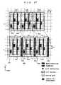
- FIG. 1is a layout of standard cells according to an embodiment 1 of the present invention.
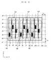
- FIG. 2is an illustration of locations of terminals according to the embodiment 1.
- FIG. 3is a layout relating to the embodiment 1 for describing a failure to locate the terminals at grid intersections.
- FIG. 4is a layout of standard cells according to a modified embodiment of the embodiment 1.
- FIG. 5is a design flow chart of an automatic placement & routing method using a standard cell according to an embodiment 2 of the present invention.
- FIG. 6is a layout of standard cells according to an embodiment 2 of the present invention.
- FIG. 7is a processing flow chart of an automatic placement & routing method using a standard cell according to an embodiment 3 of the present invention.
- FIG. 8is a layout of standard cells according to an embodiment 3 of the present invention.
- FIG. 9is a design flow chart of an automatic placement & routing method using a standard cell according to an embodiment 4 of the present invention.
- FIG. 10is a layout of standard cells according to the embodiment 4.
- FIG. 11is a layout of standard cells according to an embodiment 5 of the present invention.
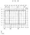
- FIG. 12is an illustration of locations of terminals according to the embodiment 5.
- FIG. 13is a layout relating to the embodiment 5 for describing a failure to locate the terminals at grid intersecting points.
- FIG. 14is a layout of a standard cell including gate electrodes having different gate lengths in the embodiment 5.
- FIG. 15is a design flow chart of an automatic placement & routing method using a standard cell according to an embodiment 6 of the present invention.
- FIG. 16is a layout of standard cells according to the embodiment 6.
- FIG. 17is a layout of standard cells according to a conventional technology.
- FIG. 18is another layout of standard cells according to the conventional technology.
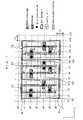
- FIG. 1is a layout of standard cells according to an embodiment 1 of the present invention.
- a direction along a power-supply wiring S of the standard cellis referred to as X direction, while a direction vertical to the power-supply wiring S is referred to as Y direction.
- the power-supply wiring Sis merely an example, and is not necessarily allocated as shown.
- x 1 -x 13denote routing grids used in automatic placement & routing and provided in the X direction
- y 1 -y 8denote routing grids provided in the Y direction
- C 1 , C 2 and C 3denote standard cells
- O 1 , O 2 and O 3are respectively origins of C 1 , C 2 and C 3
- Gdenotes a gate electrode.
- An automatic placement & routing toolis an automatic design tool for determining the location of cells and blocks and routing path among their terminals.
- the automatic design toolcomprises programs processed on a computer, and installed in the computer in advance and used.
- the wiringcan be provided with a minimum wiring width on the routing grids in the X and Y directions.
- the routing grids for the wiringsare located at the equal interval of Lx in the X direction and located at the equal interval of Ly in the Y direction.
- different wiring layersare respectively used for the wirings in the X direction and the wirings in the Y direction, and the different wiring layers are joined by means of an inter-layer connection.
- a wiring constituting the terminal Thas a rectangular shape horizontally extended along the X direction.
- a shorter-side dimension of the terminal Tcorresponds to a wiring width W in the automatic placement & routing.
- a longer-side dimensionis at least (Lx+W), where Lx is the routing grid interval and W is the wiring width.
- the terminal TIn order to provide the wiring connection for the terminal T using the automatic placement & routing tool, the terminal T must include the grid intersection (a point at which the routing grids intersect with each other) (see black circles).
- the terminal TWhen the terminal T has the rectangular shape horizontally extended wherein its longer-side dimension is (Lx+W), the terminal T intersects with the intersection of the routing grids maximally at two positions as exemplified by terminals T 11 and T 17 shown in FIG. 2 . Further, the terminal T intersects with at least one grid intersection exemplified by terminals T 12 -T 16 even when the terminal T shifts in the X direction from the positions shown by the terminals T 11 and T 17 .
- the location of the cellis restricted in the Y direction.
- the terminal Tcan be located on at least one routing grid intersection. Therefore, it becomes unnecessary to locate the origins of the respective cells at inter-grid midpoints in the X direction as shown in the cells C 51 , C 52 and C 53 according to the conventional technology shown in FIG. 17 in order to locate all of the terminals T on the routing grids.
- the additional regions R 1 , R 2 and R 3which are provided in order to locate all of the terminals Ton the routing grids, need not be provided in the cell, or the useless regions R 1 , R 2 and R 3 are no longer generated between the cells. As a result, a chip area can be reduced.
- An upper-limit value of the longer-side dimension of the wiring constituting the terminal Tis substantively a length obtained by subtracting a minimum wiring interval from the cell width of the cell C along the X direction. Further, as described, the longer-side dimension of the wiring constituting the terminal T is preferably set to (Lx+W) in terms of an area efficiency. However, the value of (Lx+W) may be regarded as a lower-limit value of the longer-side dimension of the wiring constituting the terminal T.
- the present inventionwas applied to the standard cell when logic blocks are synthesized in the design.
- the present inventioncan also be applied to a gate array cell in which a gate pitch is previously set.
- the same constitution on the drawingis obtained as far as a terminal of the gate array cell has a shape identical to that of the terminal of the standard cell.
- the effect of reducing the cell areais obtained in the same manner as in the case of the standard cell.
- the block areacan be prevented from increasing when the routing grids are extended to be equal to the gate pitch of the gate array cell.
- FIG. 1also shows a part of the semiconductor integrated circuit designed using the cell described in the embodiment 1. It is needless to say that the area of the integrated circuit can be reduced when the cell described above is used.
- the origin of the cell having the cell width not necessarily corresponding to the integral multiple of Lxmay not always be located at the midpoint between the adjacent routing grids in the X direction.
- the constitution shown in FIG. 4can achieve the same effect as obtained in the embodiment 1.
- FIG. 5is a design flow chart of an automatic placement & routing method using a standard cell according to an embodiment 2 of the present invention.
- An automatic placement & routing apparatus for implementing the automatic placement& routing methodcomprises a connection information inputting device for acquiring a connection information of a logic circuit from outside, a design constraint inputting device for acquiring a design constraint of the logic circuit from outside, a layout information inputting device for acquiring a layout information of the standard cell from outside, a tentative placing device for tentatively placing respective cells based on the acquired connection information, and a relocating device for relocating the cells tentatively placed so as to reduce an area.
- the automatic placement & routing apparatusthus constituted places and routes the logic circuit including a plurality of standard cells.
- the circuit connection information of the logic circuit for connecting the plurality of standard cells to one another, the design constraint required for the automatic placement & routing, and the layout data of the respective standard cellsare previously stored in a memory device not shown.
- the layout information stored in the memory devicerefers to the layout of cells C 21 , C 22 and C 23 having the same structure as described in the embodiment 1.
- the automatic placement & routing apparatusreads the circuit connection information, design constraint and layout data of the respective standard cells from the memory device in a data reading step S 1 .
- the automatic placement & routingtentatively places the cells C 21 , C 22 and C 23 based on the circuit connection information so that origins O 21 , O 22 and O 23 of first standard cells C 21 , C 22 and C 23 are located at the midpoints between the adjacent routing grids in the X direction and at the midpoints between the routing grids in the Y direction in a tentative placing step S 2 .
- the first standard cells C 21 , C 22 and C 23have the structure described in the embodiment 1, and each has the cell width not necessarily corresponding to the integral multiple of the routing grid interval in the automatic placement & routing.
- the automatic placement & routing apparatusextracts, from the standard cell tentatively placed, the cell in which the Y coordinate of the cell origin is located at the midpoint between the adjacent routing grids or on the routing grid in the automatic placement & routing and the X coordinate of the cell origin is located at the midpoint between the adjacent routing grids or on the routing grid in a relocating step S 3 .
- the cells C 21 , C 22 and C 23are extracted.
- the automatic placement & routing apparatusrelocates the extracted cells C 21 , C 22 and C 23 by moving them in the X direction so that the extra regions R 21 , R 22 and R 23 adjacent thereto are eliminated so that their respective cell boundaries come into contact with one another so that the area of the logic part can be reduced.
- the automatic placement & routing apparatusroutes the relocated cells C 21 , C 22 , and C 23 with respect one another in an actual routing processing step S 4 .
- the regions R 21 and R 22 (shaded regions) in the tentative placing step S 2can be eliminated.
- the logic areacan be reduced, and the chip area can be reduced.
- FIG. 7is a design flow chart of an automatic placement & routing method using a standard cell according to an embodiment 3 of the present invention.
- An automatic placement & routing apparatus for implementing the automatic placement & routing methodcomprises a connection information inputting device for acquiring a connection information of a logic circuit from outside, a design constraint inputting device for acquiring a design constraint of the logic circuit from outside, a layout information inputting device for acquiring a layout information of the standard cell from outside, a placing device for placing cells based on the acquired connection information, a tentative routing processing device for providing a tentative routing for connecting terminals of the respective cells, a terminal shape processing device. for shaping a terminal, and an actual routing processing device.
- the circuit connection information of the logic circuit for connecting a plurality of standard cells to one another, the design constraint required for the automatic placement & routing, and the layout data of the respective standard cellsare previously stored in the memory device not shown.
- the layout information stored in the memory devicebasically has a structure similar to that of the layout information relating to the cells C 11 , C 12 and C 13 having the structure described in the embodiment 1. Details of the layout information is given below.
- the automatic placement & routing apparatusreads the circuit connection information of the logic circuit for connecting the plurality of cells to one another, the design constraint required for the automatic placement & routing and the layout data of each cell from the memory device in a data reading step S 11 .
- the read layout databasically has the similar structure as described in the embodiment 1, the longer-side dimension of terminal T is set to the length obtained by subtracting the minimum wiring interval from the cell width along the X direction. The longer-side dimension of the terminal T will be reduced in a subsequent step. Further, the cell width is not necessarily the integral multiple of the routing grid interval in the automatic placement & routing.
- the automatic placement & routing apparatusplaces cells C 31 , C 32 and C 33 based on the circuit connection information so that cell origins O 31 , O 32 and O 33 are located at the midpoints between the adjacent routing grids in the Y direction in a standard cell placing step S 12 .
- the automatic placement & routing apparatusconnects the plurality of terminals T by wrings based on the circuit connection information in a tentative routing processing step S 13 . Because the shape of the terminal T is extended in the X direction, a degree of freedom in the tentative routing is increased, which reduces an entire wiring length.
- the automatic placement & routing apparatusautomatically acknowledges a shape and a dimension of the terminal demanded to realize an effective connection, and removes any unnecessary part from the terminal T to thereby reduce the dimension of the terminal in a terminal shape processing step S 14 .
- the automatic placement & routing apparatusroutes the standard cells with respect to one another in an actual routing processing step S 15 . Because the routing resource is increased by the reduction of the terminal dimension in the terminal shape processing step S 14 , the standard cells are routed with respect to one another in such manner that the increased routing resource is maximally utilized.
- the entire wiring lengthcan be reduced, and the reductions of the wiring capacity and delay time and the reduction of the design TAT because of the increased routing resource can be realized.
- the regions R 1 , R 2 and R 3need not be provided in the cell in order to locate all of the terminals T on the routing grids, or the regions R 1 , R 2 and R 3 are no longer generated between the cells. As a result, the chip area can be reduced.
- FIG. 9is a design flow chart of an automatic placement & routing method using a standard cell according to an embodiment 4 of the present invention.
- An automatic placement & routing apparatus for implementing the automatic placement & routing methodcomprises a connection information inputting device for acquiring a connection information of a logic circuit from outside, a design constraint inputting device for acquiring a design constraint of the logic circuit from outside, a layout information inputting device for acquiring a layout information of a standard cell library including cells having a cell width corresponding to the integral multiple of the routing grid interval and a layout information of a standard cell library including cells having a cell width not necessarily corresponding to the integral multiple of the routing grid interval from outside, a placing device for placing the cells of the standard cell library having the cell width corresponding to the integral multiple of the routing grid interval based on the acquired connection information, a cell replacing device for replacing the placed cells with the cells of the same logic in the standard cell library having the width not necessarily corresponding to the integral multiple of the routing grid interval, a relocating device for relocating the cells in order to reduce an area where the cells are located, and an actual routing processing device for connecting the relocated cells by wirings based on the connection
- the group of standard cells having the cell width corresponding to the integral multiple of the routing grid intervalis referred to as a first group of cells, and the group of standard cells having the cell width not necessarily corresponding to the integral multiple of the routing grid interval is referred to as a second group of cells.
- the circuit connection information of the logic circuit for connecting the plurality of standard cells to one another, the design constraint required for the automatic placement & routing, and the layout data of the respective standard cellsare previously stored in the memory device not shown.
- the layout information stored in the memory devicebasically has a structure similar to the layout information of the cells, C 11 , C 12 and C 13 having the structure described in the embodiment 1.
- the layout informationincludes the layout information of the first group of cells and the layout information of the second group of cells.
- the automatic placement & routing apparatusreads the circuit connection information of the logic circuit for connecting the plurality of standard cells to one another, the design constraint required for the automatic placement & routing, and the layout data of the first group of cells and the layout data of the second group of cells from the memory device in a data reading step S 21 .
- the automatic placement & routing apparatusplaces first cells Cb 11 , Cb 12 and Cb 13 whose layout information have been read out so that origins thereof Ob 11 , ob 12 and Ob 13 are located at the midpoints between the adjacent routing grids in the X direction and at the midpoints between the adjacent routing grids in the Y direction based on the circuit connection information as shown in FIG. 10 in a tentative placing step S 22 .
- the automatic placement & routing apparatusreplaces the first cells Cb 11 , Cb 12 and CB 13 with second cells Cb 21 , Cb 22 and Cb 23 based on the same logic in a cell replacing step S 23 .
- origins Ob 21 , Ob 22 and Ob 23 of the second cells Cb 21 , Cb 22 and Cb 23are set to have the same coordinates as the origins Ob 11 , Ob 12 and Ob 13 of the cells Cb 11 , Cb 12 and Cb 13 .
- the automatic placement & routing apparatusrelocates the second cells Cb 21 , Cb 22 and Cb 23 by shifting them in the X direction so that a total area where the cells are located is reduced in a relocating step S 24 .
- the cellsare shifted maximally to a point at which the cell boundaries of the adjacent cells are in contact with each other.
- the automatic placement & routing apparatusroutes the relocated second cells Cb 21 , Cb 22 and Cb 23 with respect to one another based on the connection information in an actual routing processing step S 25 .
- the regions Rb 21 and Rb 22 (shaded parts) shown in FIG. 10can be eliminated when the automatic placement & routing tool incapable of directly handling the second cells having the cell width not necessarily corresponding to the integral multiple of the routing grid interval is used.
- the logic area comprising the standard cellscan be reduced, and the chip area is consequently reduced.
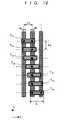
- FIG. 11is a layout of standard cells according to an embodiment 5 of the present invention.
- a direction along a power-supply wiring S of the standard cellis referred to as X direction, while a direction vertical to the power-supply wiring S is referred to as Y direction.
- the power-supply wiring Sis merely an example, and is not necessarily allocated as shown.
- x 1 -x 13denote routing grids for the automatic placement & routing disposed in parallel with the Y direction and adjacent to one another in the X direction
- y 1 -y 8denote routing grids disposed in parallel with the X direction and adjacent to one another in the Y direction
- gx 1 -gx 10denote grids of gate pitches for the automatic placement & routing disposed in parallel with the Y direction and adjacent to one another in the X direction
- C 61 , C 62 and C 63are standard cells
- O 61 , O 62 and O 63are respective origins of the standard cells C 61 , C 62 and C 63
- Gdenotes a gate electrode
- DGdenotes a dummy gate electrode.
- An automatic placement & routing toolis an automatic design tool for determining the location of cells and blocks and routing path among their terminals.
- the automatic placement & routing toolis constituted in the same manner as in the respective embodiments described earlier.
- the respective cellscan be located at the positions of the grids of the gate pitches in the X direction because the cell width of each cell in the X direction is the integral multiple of the gate pitch Gx.
- the use of the automatic 1 placement & routing toolallows the wiring to be provided on the routing grids in the X and Y directions with a minimum wiring width.
- the routing gridsare located at the equal interval of Lx different to the gate pitch Gx in the X direction, and located at the equal interval of Ly in the Y direction.
- different wiring layersare used for the wirings in the X direction and the wirings in the Y direction, and the different wiring layers are joined by means of the inter-layer connection.
- a wiring constituting the terminal Thas a rectangular shape horizontally extended along the X direction.
- a shorter-side dimension of the terminal Tcorresponds to a wiring width W in the automatic placement & routing.
- a longer-side dimensionis at least (Lx+W).
- the terminal TIn order to provide the wiring connection for the terminal T using the automatic placement & routing tool, the terminal T must include the grid intersection (a point at which the routing grids intersect with each other) (see black circles ⁇ ).
- the terminal TWhen the terminal T has the rectangular shape horizontally extended wherein its longer-side dimension is (Lx+W) as in the embodiment 5, the terminal T intersects with the intersection of the routing grids maximally at two positions as exemplified by terminals T 11 and T l7 shown in FIG. 12 . Further, the terminal T intersects with at least one grid intersection point as exemplified by terminals T 12 -T 16 even when the terminal T shifts in the X direction from the positions shown by the terminals T 11 and T 17 .
- the terminal Tcan be located at not less than one routing grid intersection even when the cells are located at an integral multiple of the gate pitch Gx different to the routing grid Lx in the X direction though the location of the cells is restricted in the Y direction. Therefore, it becomes unnecessary to locate the cell origins at the inter-grid mid points in the X direction as shown by the cells C 51 , C 52 and C 53 according to the conventional technology of FIG. 17 in order to locate all of the terminals T on the routing grids. In other words, the extra regions R 1 , R 2 and R 3 for locating all of the terminals T on the routing grids need not be provided in the cell, or the useless regions R 1 , R 2 and R 3 are no longer generated between the cells. As a result, the chip area can be reduced.
- the gate lengths and the gate intervalsare equal in the patterns of the gate electrodes and the dummy gate electrodes. Accordingly, a precision in a finished dimension of the gate electrode can be improved. Further, when the standard cells are adjacently located, the gate lengths and the gate intervals in the patterns of the gate electrodes and the dummy gate electrodes are the same as when they are located alone.
- An upper-limit value of the longer-side dimension of the wiring constituting the terminal Tis substantively a length obtained by subtracting the minimum wiring interval from the cell width of the Cell C along the X direction.
- the longer-side dimension of the wiring constituting the terminal Tis preferably (Lx+W) in terms of the area efficiency.
- the value of (Lx+W)may be regarded as the lower-limit value of the longer-side dimension of the wiring constituting the terminal T.
- the present inventionwas applied to the standard cell when logic blocks are synthesized in the design.
- the present inventioncan also be applied to a gate array cell whose gate pitch is previously set according to the embodiment 5.
- the terminal of the gate array cellshould have the shape identical to that of the terminal of the standard cell. Then, the effect of reducing the cell area is obtained in the same manner as in the case of the standard cell.
- the block areacan be prevented from increasing when the routing grids are extended to be equal to the gate pitch of the gate array cell.
- the gate lengthsare all equal in the gate electrodes and the dummy gate electrodes, however, are not necessarily be equal.
- FIG. 14shows an example of a standard cell in which the gate lengths in part of the gate electrodes and the dummy gate electrodes are not equal.
- a reference symbol C 81denotes a standard cell.
- the standard cell C 81comprises gate electrodes G, dummy gate electrodes DG and two gate electrodes G 2 having a gate length different to those of the gate electrode G and the dummy gate electrode DG, wherein a width of the gate electrode G 2 is set so that a cell width of the standard cell C 81 in the X direction is an integral multiple of the gate pitch Gx.
- the cell width of the standard cell C 81is nine times as wide as the gate pitch Gx.
- the width of the gate electrode G 2is thus set because a processing speed is expected to be faster when the cell width of each cell in the X direction is the integral multiple of the gate pitch Gx than when the cell width of each cell takes an arbitrary value in the placement using the conventional automatic placement & routing tool.
- the width of the gate electrode G 2is not necessarily set in the foregoing manner.
- the terminalsare not shown in FIG. 14 to simplify the description.
- the cell position in the X directioncan be arbitrarily set, which prevents the generation of any additional region between the cells.
- the degree of freedom in designing the standard cellis improved because the patterns of the gate electrode and the dummy gate electrode can include the uneven part in the gate length and gate interval.
- the embodiment 5can be applied in the same manner to a cell structure where the dummy gate electrodes having the different gate lengths are provided and a cell structure where the gate electrodes and the dummy gate electrodes having the different gate intervals are provided.
- the description of the embodiment 5is premised on the provision of the dummy gates DG, however, the same effect can be obtained in the same manner when the embodiment 5 is applied to a constitution where the dummy gate electrodes DG are not provided and the distance from the cell boundary of each standard cell to the gate electrode in the closest vicinity is constant.
- the distance from the cell boundary of each standard cell to the gate electrode in the closest vicinity and the distance from the cell boundary of another standard cell adjacent thereto to the gate electrode in the closest vicinityare constant. Therefore, the effect obtained in the embodiment 5, that is the OPC can be processed in each standard cell, can be realized in the same manner in the foregoing constitution.
- a distance from each of the cell boundary of the standard cells C 61 , C 62 and C 63 to the gate electrode in the X directionis “Gx ⁇ gate length/2” and constant even in the constitution shown in FIG. 11 where the dummy gate electrodes DG are not provided.
- a distance between a transistor disposed at the end of each standard cell and the gate electrode G of the adjacent standard cellis “2Gx ⁇ gate length” and constant.
- the distance from each of the cell boundary of the respective standard cells C 61 , C 62 and C 63 to the gate electrode G located at the end of each of the standard cells in the X directionis constant at (Gx ⁇ gate length/2). Further, the distance from the gate electrode G located at the end of each of the standard cells to the gate electrode G located at the end of each of adjacent standard cells in the X direction is constant at (2Gx ⁇ gate length).
- FIG. 15is a design flow chart of an automatic placement & routing method for a standard cell according to an embodiment 6 of the present invention.
- An automatic placement & routing apparatus for implementing the automatic placement & routing methodcomprises a connection information inputting device for acquiring a connection information of a logic circuit from outside, a design constraint inputting device, a layout information inputting device for acquiring a layout information of a standard cell, and a placing device for placing cells based on the acquired connection information.
- the automatic placement & routing apparatusthus constituted places and routes the logic circuit including a plurality of standard cells.
- the circuit connection information of the logic circuit for connecting the plurality of standard cells to one another, the design constraint required for the automatic placement & routing, and the layout data of the respective standard cellsare previously stored in the memory device not shown.
- the layout information stored in the memory devicerefers to the layout of the cells, C 21 , C 22 and C 23 having the structure described in the embodiment 5.
- the automatic placement & routing apparatusreads the circuit connection information of the logic circuit, design constraint and layout data of the respective standard cells from the memory device in a data reading step S 31 .
- the automatic placement & routing apparatusplaces cells C 91 , C 92 and C 93 based on the circuit connection information in a placing step S 32 .
- the cells C 91 , C 92 and C 93are located at the grid positions corresponding to the integral multiple of the gate pitch Gx that regulates the cell width in the X direction and at the midpoints between the adjacent routing grids in the Y direction as shown in FIG. 16 .
- the automatic placement & routing apparatusroutes the placed cells C 91 , C 92 and C 93 with respect to one another in an actual routing processing step S 33 .
- the cellsare located at the grid positions corresponding to the integral multiple of the gate pitch Gx that regulates the cell width in the X direction in the cell placement step S 32 so that the cell area can be reduced and the chip size is consequently reduced.
- the standard cells described in the embodiments 1 and 5are used.
- the gate lengths and the gate intervalsare thereby equal in the patterns of the gate electrodes of the placed standard cells C 91 , C 92 and C 93 , which leads to the improvement of the precision in the finished dimension of the gate electrodes.
- the improvement of the precision in the finished dimension of the gate electrodescan be realized not only inside each of the standard cells C 91 , C 92 and C 93 but also between the standard cells.
- the gate lengths and the gate intervals in the patterns of the gate electrodes and the dummy gate electrodesare the same as when they are located alone. Therefore, the OPC can be processed in each standard cell.
- An automatic placement & routing method for the standard cell shown in the embodiment 6can realize the data reading step S 21 , placing step S 22 , actual routing processing step S 23 and the like by executing an operation process using a CPU or the like. Then, a designer can input the design constraint and the like to the memory device using a keyboard or the like so that the design constraint is memorized therein, and further, confirm data during the designing process and data after the completion of the routing process via a monitor screen in the designing process.
- the present embodimentcan be realized on hardware.
Landscapes
- Engineering & Computer Science (AREA)
- Computer Hardware Design (AREA)
- Physics & Mathematics (AREA)
- Theoretical Computer Science (AREA)
- Architecture (AREA)
- Evolutionary Computation (AREA)
- Geometry (AREA)
- General Engineering & Computer Science (AREA)
- General Physics & Mathematics (AREA)
- Design And Manufacture Of Integrated Circuits (AREA)
- Semiconductor Integrated Circuits (AREA)
Abstract
Description
Claims (32)
Priority Applications (1)
| Application Number | Priority Date | Filing Date | Title |
|---|---|---|---|
| US12/359,615US20090138840A1 (en) | 2004-12-20 | 2009-01-26 | Cell, standard cell, standard cell library, a placement method using standard cell, and a semiconductor integrated circuit |
Applications Claiming Priority (6)
| Application Number | Priority Date | Filing Date | Title |
|---|---|---|---|
| JP2004-367717 | 2004-12-20 | ||
| JP2004367717 | 2004-12-20 | ||
| JP2005-191434 | 2005-06-30 | ||
| JP2005191434 | 2005-06-30 | ||
| JP2005-353654 | 2005-12-07 | ||
| JP2005353654AJP2007043049A (en) | 2004-12-20 | 2005-12-07 | Cell, standard cell, standard cell arrangement method, standard cell library, and semiconductor integrated circuit |
Related Child Applications (1)
| Application Number | Title | Priority Date | Filing Date |
|---|---|---|---|
| US12/359,615DivisionUS20090138840A1 (en) | 2004-12-20 | 2009-01-26 | Cell, standard cell, standard cell library, a placement method using standard cell, and a semiconductor integrated circuit |
Publications (2)
| Publication Number | Publication Date |
|---|---|
| US20060136848A1 US20060136848A1 (en) | 2006-06-22 |
| US7503026B2true US7503026B2 (en) | 2009-03-10 |
Family
ID=36597651
Family Applications (2)
| Application Number | Title | Priority Date | Filing Date |
|---|---|---|---|
| US11/305,191Active2027-01-30US7503026B2 (en) | 2004-12-20 | 2005-12-19 | Cell, standard cell, standard cell library, a placement method using standard cell, and a semiconductor integrated circuit |
| US12/359,615AbandonedUS20090138840A1 (en) | 2004-12-20 | 2009-01-26 | Cell, standard cell, standard cell library, a placement method using standard cell, and a semiconductor integrated circuit |
Family Applications After (1)
| Application Number | Title | Priority Date | Filing Date |
|---|---|---|---|
| US12/359,615AbandonedUS20090138840A1 (en) | 2004-12-20 | 2009-01-26 | Cell, standard cell, standard cell library, a placement method using standard cell, and a semiconductor integrated circuit |
Country Status (2)
| Country | Link |
|---|---|
| US (2) | US7503026B2 (en) |
| JP (1) | JP2007043049A (en) |
Cited By (30)
| Publication number | Priority date | Publication date | Assignee | Title |
|---|---|---|---|---|
| US20070101279A1 (en)* | 2005-10-27 | 2007-05-03 | Chaudhri Imran A | Selection of user interface elements for unified display in a display environment |
| US20080222587A1 (en)* | 2007-03-05 | 2008-09-11 | Tela Innovations, Inc. | Integrated Circuit Cell Library for Multiple Patterning |
| US20090153008A1 (en)* | 2007-12-18 | 2009-06-18 | Hitachi Displays, Ltd. | Display device |
| US7577933B1 (en)* | 2006-11-17 | 2009-08-18 | Sun Microsystems, Inc. | Timing driven pin assignment |
| US20100187627A1 (en)* | 2008-03-13 | 2010-07-29 | Tela Innovations, Inc. | Channelized Gate Level Cross-Coupled Transistor Device with Overlapping PMOS Transistors and Overlapping NMOS Transistors Relative to Direction of Gate Electrodes |
| US20110084312A1 (en)* | 2009-10-13 | 2011-04-14 | Tela Innovations, Inc. | Methods for Cell Boundary Encroachment and Layouts Implementing the Same |
| US20120273841A1 (en)* | 2007-08-02 | 2012-11-01 | Tela Innovations, Inc. | Methods for Cell Phasing and Placement in Dynamic Array Architecture and Implementation of the Same |
| US20130027083A1 (en)* | 2011-07-28 | 2013-01-31 | Takashi Ando | Semiconductor integrated circuit device |
| US8370786B1 (en)* | 2010-05-28 | 2013-02-05 | Golden Gate Technology, Inc. | Methods and software for placement improvement based on global routing |
| US8436400B2 (en) | 2006-03-09 | 2013-05-07 | Tela Innovations, Inc. | Semiconductor device with gate level including gate electrode conductors for transistors of first type and transistors of second type with some gate electrode conductors of different length |
| US8448102B2 (en) | 2006-03-09 | 2013-05-21 | Tela Innovations, Inc. | Optimizing layout of irregular structures in regular layout context |
| US8453094B2 (en) | 2008-01-31 | 2013-05-28 | Tela Innovations, Inc. | Enforcement of semiconductor structure regularity for localized transistors and interconnect |
| US8471391B2 (en) | 2008-03-27 | 2013-06-25 | Tela Innovations, Inc. | Methods for multi-wire routing and apparatus implementing same |
| US8541879B2 (en) | 2007-12-13 | 2013-09-24 | Tela Innovations, Inc. | Super-self-aligned contacts and method for making the same |
| US8653857B2 (en) | 2006-03-09 | 2014-02-18 | Tela Innovations, Inc. | Circuitry and layouts for XOR and XNOR logic |
| US8658542B2 (en) | 2006-03-09 | 2014-02-25 | Tela Innovations, Inc. | Coarse grid design methods and structures |
| US8680626B2 (en) | 2007-10-26 | 2014-03-25 | Tela Innovations, Inc. | Methods, structures, and designs for self-aligning local interconnects used in integrated circuits |
| US8756551B2 (en) | 2007-08-02 | 2014-06-17 | Tela Innovations, Inc. | Methods for designing semiconductor device with dynamic array section |
| US8839175B2 (en) | 2006-03-09 | 2014-09-16 | Tela Innovations, Inc. | Scalable meta-data objects |
| US8863063B2 (en) | 2009-05-06 | 2014-10-14 | Tela Innovations, Inc. | Finfet transistor circuit |
| US9035359B2 (en) | 2006-03-09 | 2015-05-19 | Tela Innovations, Inc. | Semiconductor chip including region including linear-shaped conductive structures forming gate electrodes and having electrical connection areas arranged relative to inner region between transistors of different types and associated methods |
| US9122832B2 (en) | 2008-08-01 | 2015-09-01 | Tela Innovations, Inc. | Methods for controlling microloading variation in semiconductor wafer layout and fabrication |
| US9159627B2 (en) | 2010-11-12 | 2015-10-13 | Tela Innovations, Inc. | Methods for linewidth modification and apparatus implementing the same |
| US9230910B2 (en) | 2006-03-09 | 2016-01-05 | Tela Innovations, Inc. | Oversized contacts and vias in layout defined by linearly constrained topology |
| US9563733B2 (en) | 2009-05-06 | 2017-02-07 | Tela Innovations, Inc. | Cell circuit and layout with linear finfet structures |
| US10276488B2 (en) | 2012-06-01 | 2019-04-30 | Taiwan Semiconductor Manufacturing Company, Ltd. | Method of fabricating field effect transistor having non-orthogonal gate electrode |
| US10410917B2 (en) | 2016-03-03 | 2019-09-10 | Samsung Electronics Co., Ltd. | Semiconductor device including standard cell and electronic design automation method thereof |
| US11024509B2 (en) | 2019-01-18 | 2021-06-01 | Samsung Electronics Co., Ltd. | Method of fabricating semiconductor device |
| US20210343697A1 (en)* | 2020-04-30 | 2021-11-04 | Taiwan Semiconductor Manufacturing Company, Ltd. | Semiconductor device having staggered gate-stub-size profile and method of manufacturing same |
| US11355604B2 (en) | 2019-10-08 | 2022-06-07 | Samsung Electronics Co., Ltd. | Semiconductor device, layout design method for the same and method for fabricating the same |
Families Citing this family (31)
| Publication number | Priority date | Publication date | Assignee | Title |
|---|---|---|---|---|
| JP2008021001A (en)* | 2006-07-11 | 2008-01-31 | Matsushita Electric Ind Co Ltd | Pattern correction device, pattern optimization device, and integrated circuit design device |
| JP2008235350A (en)* | 2007-03-16 | 2008-10-02 | Matsushita Electric Ind Co Ltd | Semiconductor integrated circuit |
| US8037441B2 (en)* | 2007-09-25 | 2011-10-11 | International Business Machines Corporation | Gridded-router based wiring on a non-gridded library |
| US8004014B2 (en) | 2008-07-04 | 2011-08-23 | Panasonic Corporation | Semiconductor integrated circuit device having metal interconnect regions placed symmetrically with respect to a cell boundary |
| US20100057473A1 (en)* | 2008-08-26 | 2010-03-04 | Hongwei Kong | Method and system for dual voice path processing in an audio codec |
| US8426978B2 (en) | 2009-02-17 | 2013-04-23 | Panasonic Corporation | Semiconductor device including a first wiring having a bending portion and a via including the bending portion |
| US8600166B2 (en)* | 2009-11-06 | 2013-12-03 | Sony Corporation | Real time hand tracking, pose classification and interface control |
| US8495551B2 (en)* | 2009-12-17 | 2013-07-23 | International Business Machines Corporation | Shaping ports in integrated circuit design |
| US9646958B2 (en)* | 2010-03-17 | 2017-05-09 | Taiwan Semiconductor Manufacturing Company, Ltd. | Integrated circuits including dummy structures and methods of forming the same |
| US8451026B2 (en)* | 2011-05-13 | 2013-05-28 | Arm Limited | Integrated circuit, method of generating a layout of an integrated circuit using standard cells, and a standard cell library providing such standard cells |
| CN103838895B (en)* | 2012-11-26 | 2017-08-11 | 北京华大九天软件有限公司 | A kind of narrow frame wiring implementation method wing wiring in flat-panel monitor design |
| US9659129B2 (en)* | 2013-05-02 | 2017-05-23 | Taiwan Semiconductor Manufacturing Company, Ltd. | Standard cell having cell height being non-integral multiple of nominal minimum pitch |
| US9501600B2 (en) | 2013-05-02 | 2016-11-22 | Taiwan Semiconductor Manufacturing Company, Ltd. | Standard cells for predetermined function having different types of layout |
| US9811626B2 (en)* | 2014-09-18 | 2017-11-07 | Samsung Electronics Co., Ltd. | Method of designing layout of semiconductor device |
| US9767248B2 (en) | 2014-09-18 | 2017-09-19 | Samsung Electronics, Co., Ltd. | Semiconductor having cross coupled structure and layout verification method thereof |
| US9704862B2 (en) | 2014-09-18 | 2017-07-11 | Samsung Electronics Co., Ltd. | Semiconductor devices and methods for manufacturing the same |
| US10026661B2 (en) | 2014-09-18 | 2018-07-17 | Samsung Electronics Co., Ltd. | Semiconductor device for testing large number of devices and composing method and test method thereof |
| US10095825B2 (en) | 2014-09-18 | 2018-10-09 | Samsung Electronics Co., Ltd. | Computer based system for verifying layout of semiconductor device and layout verify method thereof |
| KR102423878B1 (en)* | 2014-09-18 | 2022-07-22 | 삼성전자주식회사 | Semiconductor device for testing a large number of devices and composing method and test method thereof |
| KR102321605B1 (en) | 2015-04-09 | 2021-11-08 | 삼성전자주식회사 | Method for designing layout of semiconductor device and method for manufacturing semiconductor device using the same |
| US9698056B2 (en)* | 2015-04-09 | 2017-07-04 | Samsung Electronics., Ltd. | Method for designing layout of semiconductor device and method for manufacturing semiconductor device using the same |
| WO2017145906A1 (en)* | 2016-02-25 | 2017-08-31 | 株式会社ソシオネクスト | Semiconductor integrated circuit device |
| US10380307B1 (en)* | 2016-03-30 | 2019-08-13 | Silicon Technologies, Inc. | Analog design tool, cell set, and related methods, systems and equipment |
| US10605859B2 (en)* | 2016-09-14 | 2020-03-31 | Qualcomm Incorporated | Visible alignment markers/landmarks for CAD-to-silicon backside image alignment |
| KR102678555B1 (en)* | 2016-10-05 | 2024-06-26 | 삼성전자주식회사 | Integrated circuit including modified cell and method of designing the same |
| KR102699046B1 (en)* | 2016-12-15 | 2024-08-27 | 삼성전자주식회사 | Integrated circuit having vertical transistor and semiconductor device including the same |
| KR102373540B1 (en)* | 2018-04-19 | 2022-03-11 | 삼성전자주식회사 | Integrated circuit including standard cell and method and system for fabricating the same |
| CN109345607B (en)* | 2018-10-11 | 2023-02-28 | 广州前实网络科技有限公司 | Method for automatically marking EPC picture |
| DE102020132921A1 (en)* | 2020-04-30 | 2021-11-04 | Taiwan Semiconductor Manufacturing Co., Ltd. | SEMICONDUCTOR DEVICE WITH STEPPED GATE TUBE SIZE PROFILE AND METHOD OF MANUFACTURING THEREOF |
| JP2023522522A (en)* | 2021-03-17 | 2023-05-31 | チャンシン メモリー テクノロジーズ インコーポレイテッド | Integrated circuit and its layout method |
| CN115249002A (en)* | 2021-04-26 | 2022-10-28 | 联华电子股份有限公司 | IC Layout |
Citations (20)
| Publication number | Priority date | Publication date | Assignee | Title |
|---|---|---|---|---|
| US4412240A (en) | 1979-02-27 | 1983-10-25 | Fujitsu Limited | Semiconductor integrated circuit and wiring method |
| JPS6144444A (en) | 1984-08-09 | 1986-03-04 | Nec Corp | Semiconductor ic |
| JPS6247148A (en) | 1985-08-27 | 1987-02-28 | Toshiba Corp | Semiconductor integrated circuit device |
| JPH03205849A (en) | 1990-01-08 | 1991-09-09 | Hitachi Ltd | Cell layout method |
| US5168342A (en) | 1989-01-30 | 1992-12-01 | Hitachi, Ltd. | Semiconductor integrated circuit device and manufacturing method of the same |
| JPH05136356A (en) | 1991-11-13 | 1993-06-01 | Nec Corp | Semiconductor integrated circuit |
| US5369046A (en) | 1991-04-08 | 1994-11-29 | Texas Instruments Incorporated | Method for forming a gate array base cell |
| US5448088A (en) | 1993-07-01 | 1995-09-05 | Mitsubishi Electric Engineering Company Limited | Semiconductor integrated circuit having lengthened connection pins for connection to external wirings |
| JPH09289251A (en) | 1996-04-23 | 1997-11-04 | Matsushita Electric Ind Co Ltd | Layout structure of semiconductor integrated circuit and its verification method |
| JPH1032253A (en) | 1996-07-15 | 1998-02-03 | Toshiba Corp | Semiconductor device and its manufacturing method, basic cell library and its forming method, mask |
| JPH1041398A (en) | 1996-04-10 | 1998-02-13 | Toshiba Corp | Semiconductor integrated circuit device |
| US5977574A (en)* | 1997-03-28 | 1999-11-02 | Lsi Logic Corporation | High density gate array cell architecture with sharing of well taps between cells |
| US6084256A (en) | 1996-04-10 | 2000-07-04 | Kabushiki Kaisha Toshiba | Semiconductor integrated circuit device |
| US6207479B1 (en) | 1999-06-14 | 2001-03-27 | Taiwan Semiconductor Manufacturing Co., Ltd. | Place and route method for integrated circuit design |
| US6252427B1 (en) | 1999-04-27 | 2001-06-26 | Matsushita Electronics Corporation | CMOS inverter and standard cell using the same |
| JP2002026125A (en) | 2000-07-10 | 2002-01-25 | Mitsubishi Electric Corp | Semiconductor device |
| US20020014899A1 (en)* | 2000-02-03 | 2002-02-07 | Hitachi, Ltd. | Semiconductor integrated circuit |
| US20020087940A1 (en)* | 2000-09-06 | 2002-07-04 | Greidinger Yaacov I. | Method for designing large standard-cell based integrated circuits |
| JP2004055823A (en) | 2002-07-19 | 2004-02-19 | Renesas Technology Corp | Semiconductor integrated circuit |
| US6897496B2 (en) | 2000-11-30 | 2005-05-24 | Hitachi, Ltd. | Semiconductor device, a method of manufacturing the same and storage media |
Family Cites Families (5)
| Publication number | Priority date | Publication date | Assignee | Title |
|---|---|---|---|---|
| JP2703224B2 (en)* | 1987-03-12 | 1998-01-26 | 株式会社東芝 | Function block automatic generation method for semiconductor integrated circuit device |
| JP2862039B2 (en)* | 1992-08-25 | 1999-02-24 | 日本電気株式会社 | Automatic layout system |
| JP3231741B2 (en)* | 1999-06-28 | 2001-11-26 | エヌイーシーマイクロシステム株式会社 | Standard cell, standard cell row, standard cell placement and routing device and placement and routing method |
| US6525350B1 (en)* | 1999-07-16 | 2003-02-25 | Kawasaki Steel Corporation | Semiconductor integrated circuit basic cell semiconductor integrated circuit using the same |
| JP2004342757A (en)* | 2003-05-14 | 2004-12-02 | Toshiba Corp | Semiconductor integrated circuit and design method thereof |
- 2005
- 2005-12-07JPJP2005353654Apatent/JP2007043049A/enactivePending
- 2005-12-19USUS11/305,191patent/US7503026B2/enactiveActive
- 2009
- 2009-01-26USUS12/359,615patent/US20090138840A1/ennot_activeAbandoned
Patent Citations (24)
| Publication number | Priority date | Publication date | Assignee | Title |
|---|---|---|---|---|
| US4412240A (en) | 1979-02-27 | 1983-10-25 | Fujitsu Limited | Semiconductor integrated circuit and wiring method |
| JPS6144444A (en) | 1984-08-09 | 1986-03-04 | Nec Corp | Semiconductor ic |
| JPS6247148A (en) | 1985-08-27 | 1987-02-28 | Toshiba Corp | Semiconductor integrated circuit device |
| US5168342A (en) | 1989-01-30 | 1992-12-01 | Hitachi, Ltd. | Semiconductor integrated circuit device and manufacturing method of the same |
| JPH03205849A (en) | 1990-01-08 | 1991-09-09 | Hitachi Ltd | Cell layout method |
| US5369046A (en) | 1991-04-08 | 1994-11-29 | Texas Instruments Incorporated | Method for forming a gate array base cell |
| JPH05136356A (en) | 1991-11-13 | 1993-06-01 | Nec Corp | Semiconductor integrated circuit |
| US5448088A (en) | 1993-07-01 | 1995-09-05 | Mitsubishi Electric Engineering Company Limited | Semiconductor integrated circuit having lengthened connection pins for connection to external wirings |
| JPH1041398A (en) | 1996-04-10 | 1998-02-13 | Toshiba Corp | Semiconductor integrated circuit device |
| US6084256A (en) | 1996-04-10 | 2000-07-04 | Kabushiki Kaisha Toshiba | Semiconductor integrated circuit device |
| JPH09289251A (en) | 1996-04-23 | 1997-11-04 | Matsushita Electric Ind Co Ltd | Layout structure of semiconductor integrated circuit and its verification method |
| US6194252B1 (en) | 1996-07-15 | 2001-02-27 | Kabushiki Kaisha Toshiba | Semiconductor device and manufacturing method for the same, basic cell library and manufacturing method for the same, and mask |
| JPH1032253A (en) | 1996-07-15 | 1998-02-03 | Toshiba Corp | Semiconductor device and its manufacturing method, basic cell library and its forming method, mask |
| US5847421A (en) | 1996-07-15 | 1998-12-08 | Kabushiki Kaisha Toshiba | Logic cell having efficient optical proximity effect correction |
| US5977574A (en)* | 1997-03-28 | 1999-11-02 | Lsi Logic Corporation | High density gate array cell architecture with sharing of well taps between cells |
| US6252427B1 (en) | 1999-04-27 | 2001-06-26 | Matsushita Electronics Corporation | CMOS inverter and standard cell using the same |
| US6207479B1 (en) | 1999-06-14 | 2001-03-27 | Taiwan Semiconductor Manufacturing Co., Ltd. | Place and route method for integrated circuit design |
| US20020014899A1 (en)* | 2000-02-03 | 2002-02-07 | Hitachi, Ltd. | Semiconductor integrated circuit |
| JP2002026125A (en) | 2000-07-10 | 2002-01-25 | Mitsubishi Electric Corp | Semiconductor device |
| US6635935B2 (en) | 2000-07-10 | 2003-10-21 | Mitsubishi Denki Kabushiki Kaisha | Semiconductor device cell having regularly sized and arranged features |
| US20020087940A1 (en)* | 2000-09-06 | 2002-07-04 | Greidinger Yaacov I. | Method for designing large standard-cell based integrated circuits |
| US6897496B2 (en) | 2000-11-30 | 2005-05-24 | Hitachi, Ltd. | Semiconductor device, a method of manufacturing the same and storage media |
| JP2004055823A (en) | 2002-07-19 | 2004-02-19 | Renesas Technology Corp | Semiconductor integrated circuit |
| US6787823B2 (en) | 2002-07-19 | 2004-09-07 | Renesas Technology Corp. | Semiconductor device having cell-based basic element aggregate having protruding part in active region |
Non-Patent Citations (1)
| Title |
|---|
| Chinese Office Action (and English Translation thereof) issued in Chinese Patent Application No. CN 200510132639.6, dated Feb. 1, 2008. |
Cited By (135)
| Publication number | Priority date | Publication date | Assignee | Title |
|---|---|---|---|---|
| US20070101279A1 (en)* | 2005-10-27 | 2007-05-03 | Chaudhri Imran A | Selection of user interface elements for unified display in a display environment |
| US9589091B2 (en) | 2006-03-09 | 2017-03-07 | Tela Innovations, Inc. | Scalable meta-data objects |
| US9443947B2 (en) | 2006-03-09 | 2016-09-13 | Tela Innovations, Inc. | Semiconductor chip including region having integrated circuit transistor gate electrodes formed by various conductive structures of specified shape and position and method for manufacturing the same |
| US10230377B2 (en) | 2006-03-09 | 2019-03-12 | Tela Innovations, Inc. | Circuitry and layouts for XOR and XNOR logic |
| US10186523B2 (en) | 2006-03-09 | 2019-01-22 | Tela Innovations, Inc. | Semiconductor chip having region including gate electrode features formed in part from rectangular layout shapes on gate horizontal grid and first-metal structures formed in part from rectangular layout shapes on at least eight first-metal gridlines of first-metal vertical grid |
| US10141334B2 (en) | 2006-03-09 | 2018-11-27 | Tela Innovations, Inc. | Semiconductor chip including region having rectangular-shaped gate structures and first-metal structures |
| US10141335B2 (en) | 2006-03-09 | 2018-11-27 | Tela Innovations, Inc. | Semiconductor CIP including region having rectangular-shaped gate structures and first metal structures |
| US9917056B2 (en) | 2006-03-09 | 2018-03-13 | Tela Innovations, Inc. | Coarse grid design methods and structures |
| US9905576B2 (en) | 2006-03-09 | 2018-02-27 | Tela Innovations, Inc. | Semiconductor chip including region having rectangular-shaped gate structures and first metal structures |
| US9859277B2 (en) | 2006-03-09 | 2018-01-02 | Tela Innovations, Inc. | Methods, structures, and designs for self-aligning local interconnects used in integrated circuits |
| US9754878B2 (en) | 2006-03-09 | 2017-09-05 | Tela Innovations, Inc. | Semiconductor chip including a chip level based on a layout that includes both regular and irregular wires |
| US9425273B2 (en) | 2006-03-09 | 2016-08-23 | Tela Innovations, Inc. | Semiconductor chip including integrated circuit including at least five gate level conductive structures having particular spatial and electrical relationship and method for manufacturing the same |
| US9711495B2 (en) | 2006-03-09 | 2017-07-18 | Tela Innovations, Inc. | Oversized contacts and vias in layout defined by linearly constrained topology |
| US8436400B2 (en) | 2006-03-09 | 2013-05-07 | Tela Innovations, Inc. | Semiconductor device with gate level including gate electrode conductors for transistors of first type and transistors of second type with some gate electrode conductors of different length |
| US8448102B2 (en) | 2006-03-09 | 2013-05-21 | Tela Innovations, Inc. | Optimizing layout of irregular structures in regular layout context |
| US9673825B2 (en) | 2006-03-09 | 2017-06-06 | Tela Innovations, Inc. | Circuitry and layouts for XOR and XNOR logic |
| US8823062B2 (en) | 2006-03-09 | 2014-09-02 | Tela Innovations, Inc. | Integrated circuit with offset line end spacings in linear gate electrode level |
| US10217763B2 (en) | 2006-03-09 | 2019-02-26 | Tela Innovations, Inc. | Semiconductor chip having region including gate electrode features of rectangular shape on gate horizontal grid and first-metal structures of rectangular shape on at least eight first-metal gridlines of first-metal vertical grid |
| US20130168778A1 (en)* | 2006-03-09 | 2013-07-04 | Scott T. Becker | Integrated Circuit Including Gate Electrode Tracks That Each Form Gate Electrodes of Different Transistor Types With Intervening Non-Gate-Forming Gate Electrode Track |
| US9741719B2 (en) | 2006-03-09 | 2017-08-22 | Tela Innovations, Inc. | Methods, structures, and designs for self-aligning local interconnects used in integrated circuits |
| US9425272B2 (en) | 2006-03-09 | 2016-08-23 | Tela Innovations, Inc. | Semiconductor chip including integrated circuit including four transistors of first transistor type and four transistors of second transistor type with electrical connections between various transistors and methods for manufacturing the same |
| US9425145B2 (en) | 2006-03-09 | 2016-08-23 | Tela Innovations, Inc. | Oversized contacts and vias in layout defined by linearly constrained topology |
| US9336344B2 (en) | 2006-03-09 | 2016-05-10 | Tela Innovations, Inc. | Coarse grid design methods and structures |
| US9240413B2 (en) | 2006-03-09 | 2016-01-19 | Tela Innovations, Inc. | Methods, structures, and designs for self-aligning local interconnects used in integrated circuits |
| US9230910B2 (en) | 2006-03-09 | 2016-01-05 | Tela Innovations, Inc. | Oversized contacts and vias in layout defined by linearly constrained topology |
| US9035359B2 (en) | 2006-03-09 | 2015-05-19 | Tela Innovations, Inc. | Semiconductor chip including region including linear-shaped conductive structures forming gate electrodes and having electrical connection areas arranged relative to inner region between transistors of different types and associated methods |
| US9009641B2 (en) | 2006-03-09 | 2015-04-14 | Tela Innovations, Inc. | Circuits with linear finfet structures |
| US8952425B2 (en) | 2006-03-09 | 2015-02-10 | Tela Innovations, Inc. | Integrated circuit including at least four linear-shaped conductive structures having extending portions of different length |
| US8946781B2 (en) | 2006-03-09 | 2015-02-03 | Tela Innovations, Inc. | Integrated circuit including gate electrode conductive structures with different extension distances beyond contact |
| US8921897B2 (en) | 2006-03-09 | 2014-12-30 | Tela Innovations, Inc. | Integrated circuit with gate electrode conductive structures having offset ends |
| US8921896B2 (en) | 2006-03-09 | 2014-12-30 | Tela Innovations, Inc. | Integrated circuit including linear gate electrode structures having different extension distances beyond contact |
| US8653857B2 (en) | 2006-03-09 | 2014-02-18 | Tela Innovations, Inc. | Circuitry and layouts for XOR and XNOR logic |
| US8658542B2 (en) | 2006-03-09 | 2014-02-25 | Tela Innovations, Inc. | Coarse grid design methods and structures |
| US8839175B2 (en) | 2006-03-09 | 2014-09-16 | Tela Innovations, Inc. | Scalable meta-data objects |
| US7577933B1 (en)* | 2006-11-17 | 2009-08-18 | Sun Microsystems, Inc. | Timing driven pin assignment |
| US8667443B2 (en) | 2007-03-05 | 2014-03-04 | Tela Innovations, Inc. | Integrated circuit cell library for multiple patterning |
| US20080222587A1 (en)* | 2007-03-05 | 2008-09-11 | Tela Innovations, Inc. | Integrated Circuit Cell Library for Multiple Patterning |
| US10074640B2 (en) | 2007-03-05 | 2018-09-11 | Tela Innovations, Inc. | Integrated circuit cell library for multiple patterning |
| US9633987B2 (en) | 2007-03-05 | 2017-04-25 | Tela Innovations, Inc. | Integrated circuit cell library for multiple patterning |
| US9424387B2 (en)* | 2007-03-07 | 2016-08-23 | Tela Innovations, Inc. | Methods for cell phasing and placement in dynamic array architecture and implementation of the same |
| US20150143321A1 (en)* | 2007-03-07 | 2015-05-21 | Tela Innovations, Inc. | Methods for Cell Phasing and Placement in Dynamic Array Architecture and Implementation of the Same |
| US8966424B2 (en) | 2007-03-07 | 2015-02-24 | Tela Innovations, Inc. | Methods for cell phasing and placement in dynamic array architecture and implementation of the same |
| US9910950B2 (en)* | 2007-03-07 | 2018-03-06 | Tela Innovations, Inc. | Methods for cell phasing and placement in dynamic array architecture and implementation of the same |
| US9595515B2 (en) | 2007-03-07 | 2017-03-14 | Tela Innovations, Inc. | Semiconductor chip including integrated circuit defined within dynamic array section |
| US8549455B2 (en)* | 2007-08-02 | 2013-10-01 | Tela Innovations, Inc. | Methods for cell phasing and placement in dynamic array architecture and implementation of the same |
| US8756551B2 (en) | 2007-08-02 | 2014-06-17 | Tela Innovations, Inc. | Methods for designing semiconductor device with dynamic array section |
| US20120273841A1 (en)* | 2007-08-02 | 2012-11-01 | Tela Innovations, Inc. | Methods for Cell Phasing and Placement in Dynamic Array Architecture and Implementation of the Same |
| US8759882B2 (en) | 2007-08-02 | 2014-06-24 | Tela Innovations, Inc. | Semiconductor device with dynamic array sections defined and placed according to manufacturing assurance halos |
| US8680626B2 (en) | 2007-10-26 | 2014-03-25 | Tela Innovations, Inc. | Methods, structures, and designs for self-aligning local interconnects used in integrated circuits |
| US10734383B2 (en) | 2007-10-26 | 2020-08-04 | Tela Innovations, Inc. | Methods, structures, and designs for self-aligning local interconnects used in integrated circuits |
| US8541879B2 (en) | 2007-12-13 | 2013-09-24 | Tela Innovations, Inc. | Super-self-aligned contacts and method for making the same |
| US9818747B2 (en) | 2007-12-13 | 2017-11-14 | Tela Innovations, Inc. | Super-self-aligned contacts and method for making the same |
| US8951916B2 (en) | 2007-12-13 | 2015-02-10 | Tela Innovations, Inc. | Super-self-aligned contacts and method for making the same |
| US9281371B2 (en) | 2007-12-13 | 2016-03-08 | Tela Innovations, Inc. | Super-self-aligned contacts and method for making the same |
| US10461081B2 (en) | 2007-12-13 | 2019-10-29 | Tel Innovations, Inc. | Super-self-aligned contacts and method for making the same |
| US7924390B2 (en)* | 2007-12-18 | 2011-04-12 | Hitachi Displays, Ltd. | Display device |
| US20090153008A1 (en)* | 2007-12-18 | 2009-06-18 | Hitachi Displays, Ltd. | Display device |
| US8453094B2 (en) | 2008-01-31 | 2013-05-28 | Tela Innovations, Inc. | Enforcement of semiconductor structure regularity for localized transistors and interconnect |
| US9530734B2 (en) | 2008-01-31 | 2016-12-27 | Tela Innovations, Inc. | Enforcement of semiconductor structure regularity for localized transistors and interconnect |
| US9202779B2 (en) | 2008-01-31 | 2015-12-01 | Tela Innovations, Inc. | Enforcement of semiconductor structure regularity for localized transistors and interconnect |
| US8701071B2 (en) | 2008-01-31 | 2014-04-15 | Tela Innovations, Inc. | Enforcement of semiconductor structure regularity for localized transistors and interconnect |
| US9245081B2 (en) | 2008-03-13 | 2016-01-26 | Tela Innovations, Inc. | Semiconductor chip including digital logic circuit including at least nine linear-shaped conductive structures collectively forming gate electrodes of at least six transistors with some transistors forming cross-coupled transistor configuration and associated methods |
| US20100187618A1 (en)* | 2008-03-13 | 2010-07-29 | Tela Innovations, Inc. | Linear Gate Level Cross-Coupled Transistor Device with Overlapping PMOS Transistors and Non-Overlapping NMOS Transistors Relative to Direction of Gate Electrodes |
| US8866197B2 (en) | 2008-03-13 | 2014-10-21 | Tela Innovations, Inc. | Integrated circuit including cross-coupled transistors having gate electrodes formed within gate level feature layout channels with at least two gate electrodes electrically connected to each other through another transistor forming gate level feature |
| US8872283B2 (en) | 2008-03-13 | 2014-10-28 | Tela Innovations, Inc. | Integrated circuit including cross-coupled transistors having gate electrodes formed within gate level feature layout channels with shared diffusion regions on opposite sides of two-transistor-forming gate level feature |
| US8592872B2 (en) | 2008-03-13 | 2013-11-26 | Tela Innovations, Inc. | Integrated circuit including cross-coupled transistors with two transistors of different type having gate electrodes formed by common gate level feature with shared diffusion regions on opposite sides of common gate level feature |
| US8587034B2 (en) | 2008-03-13 | 2013-11-19 | Tela Innovations, Inc. | Integrated circuit including cross-coupled transistors having gate electrodes formed within gate level feature layout channels with four inside positioned gate contacts and electrical connection of transistor gates through linear interconnect conductors in single interconnect layer |
| US8581303B2 (en) | 2008-03-13 | 2013-11-12 | Tela Innovations, Inc. | Integrated circuit including cross-coupled trasistors having gate electrodes formed within gate level feature layout channels with four inside positioned gate contacts having offset relationships and electrical connection of cross-coupled transistors through same interconnect layer |
| US8853793B2 (en) | 2008-03-13 | 2014-10-07 | Tela Innovations, Inc. | Integrated circuit including gate electrode level region including cross-coupled transistors having gate contacts located over inner portion of gate electrode level region and offset gate level feature line ends |
| US8581304B2 (en) | 2008-03-13 | 2013-11-12 | Tela Innovations, Inc. | Integrated circuit including cross-coupled transistors having gate electrodes formed within gate level feature layout channels with four inside positioned gate contacts having offset and aligned relationships |
| US8853794B2 (en) | 2008-03-13 | 2014-10-07 | Tela Innovations, Inc. | Integrated circuit within semiconductor chip including cross-coupled transistor configuration |
| US8575706B2 (en) | 2008-03-13 | 2013-11-05 | Tela Innovations, Inc. | Integrated circuit including cross-coupled transistors having gate electrodes formed within gate level feature layout channels with at least two different gate level features inner extensions beyond gate electrode |
| US8569841B2 (en) | 2008-03-13 | 2013-10-29 | Tela Innovations, Inc. | Integrated circuit including cross-coupled transistors having gate electrodes formed within gate level feature layout channels with at least one gate level feature extending into adjacent gate level feature layout channel |
| US8847331B2 (en) | 2008-03-13 | 2014-09-30 | Tela Innovations, Inc. | Semiconductor chip including region having cross-coupled transistor configuration with offset electrical connection areas on gate electrode forming conductive structures and at least two different inner extension distances of gate electrode forming conductive structures |
| US9081931B2 (en) | 2008-03-13 | 2015-07-14 | Tela Innovations, Inc. | Cross-coupled transistor circuit having diffusion regions of common node on opposing sides of same gate electrode track and gate node connection through single interconnect layer |
| US9117050B2 (en) | 2008-03-13 | 2015-08-25 | Tela Innovations, Inc. | Integrated circuit including cross-coupled transistors having gate electrodes formed within gate level feature layout channels with gate contact position and offset specifications |
| US8680583B2 (en) | 2008-03-13 | 2014-03-25 | Tela Innovations, Inc. | Integrated circuit including cross-coupled transistors having gate electrodes formed within at least nine gate level feature layout channels |
| US10727252B2 (en) | 2008-03-13 | 2020-07-28 | Tela Innovations, Inc. | Semiconductor chip including integrated circuit having cross-coupled transistor configuration and method for manufacturing the same |
| US8847329B2 (en) | 2008-03-13 | 2014-09-30 | Tela Innovations, Inc. | Cross-coupled transistor circuit defined having diffusion regions of common node on opposing sides of same gate electrode track with at least two non-inner positioned gate contacts |
| US9208279B2 (en) | 2008-03-13 | 2015-12-08 | Tela Innovations, Inc. | Semiconductor chip including digital logic circuit including linear-shaped conductive structures having electrical connection areas located within inner region between transistors of different type and associated methods |
| US9213792B2 (en) | 2008-03-13 | 2015-12-15 | Tela Innovations, Inc. | Semiconductor chip including digital logic circuit including at least six transistors with some transistors forming cross-coupled transistor configuration and associated methods |
| US8564071B2 (en) | 2008-03-13 | 2013-10-22 | Tela Innovations, Inc. | Integrated circuit including cross-coupled transistors having gate electrodes formed within gate level feature layout channels with at least two different gate level feature extensions beyond contact |
| US8558322B2 (en) | 2008-03-13 | 2013-10-15 | Tela Innovations, Inc. | Integrated circuit including cross-coupled transistors having gate electrodes formed within gate level feature layout channels with at least two gate electrodes electrically connected to each other through gate level feature |
| US8669594B2 (en) | 2008-03-13 | 2014-03-11 | Tela Innovations, Inc. | Integrated circuit including cross-coupled transistors having gate electrodes formed within at least twelve gate level feature layout channels |
| US10658385B2 (en) | 2008-03-13 | 2020-05-19 | Tela Innovations, Inc. | Cross-coupled transistor circuit defined on four gate electrode tracks |
| US10651200B2 (en) | 2008-03-13 | 2020-05-12 | Tela Innovations, Inc. | Cross-coupled transistor circuit defined on three gate electrode tracks |
| US8552508B2 (en) | 2008-03-13 | 2013-10-08 | Tela Innovations, Inc. | Integrated circuit including cross-coupled transistors having gate electrodes formed within gate level feature layout channels with shared diffusion regions on opposite sides of two-transistor-forming gate level feature and electrical connection of transistor gates through linear interconnect conductors in single interconnect layer |
| US8729606B2 (en) | 2008-03-13 | 2014-05-20 | Tela Innovations, Inc. | Integrated circuit including cross-coupled transistors having gate electrodes formed within gate level feature layout channels |
| US8552509B2 (en) | 2008-03-13 | 2013-10-08 | Tela Innovations, Inc. | Integrated circuit including cross-coupled transistors having gate electrodes formed within gate level feature layout channels with other transistors positioned between cross-coupled transistors |
| US8836045B2 (en) | 2008-03-13 | 2014-09-16 | Tela Innovations, Inc. | Cross-coupled transistor circuit having diffusion regions of common node on opposing sides of same gate electrode track |
| US8835989B2 (en) | 2008-03-13 | 2014-09-16 | Tela Innovations, Inc. | Integrated circuit including cross-coupled transistors having gate electrodes formed within gate level feature layout channels with gate electrode placement specifications |
| US8669595B2 (en) | 2008-03-13 | 2014-03-11 | Tela Innovations, Inc. | Integrated circuit including cross-coupled transistors having gate electrodes formed within gate level feature layout channels with gate contact position, alignment, and offset specifications |
| US8729643B2 (en) | 2008-03-13 | 2014-05-20 | Tela Innovations, Inc. | Cross-coupled transistor circuit including offset inner gate contacts |
| US8816402B2 (en) | 2008-03-13 | 2014-08-26 | Tela Innovations, Inc. | Integrated circuit including cross-coupled transistors having gate electrodes formed within gate level feature layout channels with gate level feature layout channel including single transistor |
| US8735995B2 (en) | 2008-03-13 | 2014-05-27 | Tela Innovations, Inc. | Cross-coupled transistor circuit defined on three gate electrode tracks with diffusion regions of common node on opposing sides of same gate electrode track |
| US9536899B2 (en) | 2008-03-13 | 2017-01-03 | Tela Innovations, Inc. | Semiconductor chip including integrated circuit having cross-coupled transistor configuration and method for manufacturing the same |
| US20100187627A1 (en)* | 2008-03-13 | 2010-07-29 | Tela Innovations, Inc. | Channelized Gate Level Cross-Coupled Transistor Device with Overlapping PMOS Transistors and Overlapping NMOS Transistors Relative to Direction of Gate Electrodes |
| US20100187621A1 (en)* | 2008-03-13 | 2010-07-29 | Tela Innovations, Inc. | Linear Gate Level Cross-Coupled Transistor Device with Constant Gate Electrode Pitch |
| US8785978B2 (en) | 2008-03-13 | 2014-07-22 | Tela Innovations, Inc. | Integrated circuit including cross-coupled transistors having gate electrodes formed within gate level feature layout channels with electrical connection of cross-coupled transistors through same interconnect layer |
| US8735944B2 (en) | 2008-03-13 | 2014-05-27 | Tela Innovations, Inc. | Integrated circuit including cross-coupled transistors having gate electrodes formed within gate level feature layout channels with serially connected transistors |
| US8785979B2 (en) | 2008-03-13 | 2014-07-22 | Tela Innovations, Inc. | Integrated circuit including cross-coupled transistors having gate electrodes formed within gate level feature layout channels with two inside positioned gate contacts and two outside positioned gate contacts and electrical connection of cross-coupled transistors through same interconnect layer |
| US8772839B2 (en) | 2008-03-13 | 2014-07-08 | Tela Innovations, Inc. | Integrated circuit including cross-coupled transistors having gate electrodes formed within gate level feature layout channels with four inside positioned gate contacts having offset and aligned relationships and electrical connection of transistor gates through linear interconnect conductors in single interconnect layer |
| US10020321B2 (en) | 2008-03-13 | 2018-07-10 | Tela Innovations, Inc. | Cross-coupled transistor circuit defined on two gate electrode tracks |
| US20100258879A1 (en)* | 2008-03-13 | 2010-10-14 | Tela Innovations, Inc. | Channelized Gate Level Cross-Coupled Transistor Device with Cross-Coupled Transistor Gate Electrode Connections Made Using Linear First Interconnect Level above Gate Electrode Level |
| US8742463B2 (en) | 2008-03-13 | 2014-06-03 | Tela Innovations, Inc. | Integrated circuit including cross-coupled transistors having gate electrodes formed within gate level feature layout channels with outer positioned gate contacts |
| US8742462B2 (en) | 2008-03-13 | 2014-06-03 | Tela Innovations, Inc. | Integrated circuit including cross-coupled transistors having gate electrodes formed within gate level feature layout channels with gate contact position specifications |
| US9871056B2 (en) | 2008-03-13 | 2018-01-16 | Tela Innovations, Inc. | Semiconductor chip including integrated circuit having cross-coupled transistor configuration and method for manufacturing the same |
| US8471391B2 (en) | 2008-03-27 | 2013-06-25 | Tela Innovations, Inc. | Methods for multi-wire routing and apparatus implementing same |
| US9779200B2 (en) | 2008-03-27 | 2017-10-03 | Tela Innovations, Inc. | Methods for multi-wire routing and apparatus implementing same |
| US8759985B2 (en) | 2008-03-27 | 2014-06-24 | Tela Innovations, Inc. | Methods for multi-wire routing and apparatus implementing same |
| US9390215B2 (en) | 2008-03-27 | 2016-07-12 | Tela Innovations, Inc. | Methods for multi-wire routing and apparatus implementing same |
| US9122832B2 (en) | 2008-08-01 | 2015-09-01 | Tela Innovations, Inc. | Methods for controlling microloading variation in semiconductor wafer layout and fabrication |
| US10446536B2 (en) | 2009-05-06 | 2019-10-15 | Tela Innovations, Inc. | Cell circuit and layout with linear finfet structures |
| US8863063B2 (en) | 2009-05-06 | 2014-10-14 | Tela Innovations, Inc. | Finfet transistor circuit |
| US9563733B2 (en) | 2009-05-06 | 2017-02-07 | Tela Innovations, Inc. | Cell circuit and layout with linear finfet structures |
| US8661392B2 (en)* | 2009-10-13 | 2014-02-25 | Tela Innovations, Inc. | Methods for cell boundary encroachment and layouts implementing the Same |
| US20170104004A1 (en)* | 2009-10-13 | 2017-04-13 | Tela Innovations, Inc. | Methods for Cell Boundary Encroachment and Semiconductor Devices Implementing the Same |
| US9530795B2 (en)* | 2009-10-13 | 2016-12-27 | Tela Innovations, Inc. | Methods for cell boundary encroachment and semiconductor devices implementing the same |
| US20110084312A1 (en)* | 2009-10-13 | 2011-04-14 | Tela Innovations, Inc. | Methods for Cell Boundary Encroachment and Layouts Implementing the Same |
| US20140167117A1 (en)* | 2009-10-13 | 2014-06-19 | Tela Innovations, Inc. | Methods for Cell Boundary Encroachment and Layouts Implementing the Same |
| US9269702B2 (en)* | 2009-10-13 | 2016-02-23 | Tela Innovations, Inc. | Methods for cell boundary encroachment and layouts implementing the same |
| US8370786B1 (en)* | 2010-05-28 | 2013-02-05 | Golden Gate Technology, Inc. | Methods and software for placement improvement based on global routing |
| US9704845B2 (en) | 2010-11-12 | 2017-07-11 | Tela Innovations, Inc. | Methods for linewidth modification and apparatus implementing the same |
| US9159627B2 (en) | 2010-11-12 | 2015-10-13 | Tela Innovations, Inc. | Methods for linewidth modification and apparatus implementing the same |
| US8525552B2 (en)* | 2011-07-28 | 2013-09-03 | Panasonic Corporation | Semiconductor integrated circuit device having a plurality of standard cells for leakage current suppression |
| US20130027083A1 (en)* | 2011-07-28 | 2013-01-31 | Takashi Ando | Semiconductor integrated circuit device |
| US11211323B2 (en) | 2012-06-01 | 2021-12-28 | Taiwan Semiconductor Manufacturing Company, Ltd. | Method of fabricating field effect transistor having non-orthogonal gate electrode |
| US10276488B2 (en) | 2012-06-01 | 2019-04-30 | Taiwan Semiconductor Manufacturing Company, Ltd. | Method of fabricating field effect transistor having non-orthogonal gate electrode |
| US10410917B2 (en) | 2016-03-03 | 2019-09-10 | Samsung Electronics Co., Ltd. | Semiconductor device including standard cell and electronic design automation method thereof |
| US11024509B2 (en) | 2019-01-18 | 2021-06-01 | Samsung Electronics Co., Ltd. | Method of fabricating semiconductor device |
| US12074031B2 (en) | 2019-01-18 | 2024-08-27 | Samsung Electronics Co., Ltd. | Method of fabricating semiconductor device |
| US11355604B2 (en) | 2019-10-08 | 2022-06-07 | Samsung Electronics Co., Ltd. | Semiconductor device, layout design method for the same and method for fabricating the same |
| US11916120B2 (en) | 2019-10-08 | 2024-02-27 | Samsung Electronics Co., Ltd. | Semiconductor device, layout design method for the same and method for fabricating the same |
| US20210343697A1 (en)* | 2020-04-30 | 2021-11-04 | Taiwan Semiconductor Manufacturing Company, Ltd. | Semiconductor device having staggered gate-stub-size profile and method of manufacturing same |
| US11842994B2 (en)* | 2020-04-30 | 2023-12-12 | Taiwan Semiconductor Manufacturing Company, Ltd | Semiconductor device having staggered gate-stub-size profile and method of manufacturing same |
Also Published As
| Publication number | Publication date |
|---|---|
| JP2007043049A (en) | 2007-02-15 |
| US20060136848A1 (en) | 2006-06-22 |
| US20090138840A1 (en) | 2009-05-28 |
Similar Documents
| Publication | Publication Date | Title |
|---|---|---|
| US7503026B2 (en) | Cell, standard cell, standard cell library, a placement method using standard cell, and a semiconductor integrated circuit | |
| US8516428B2 (en) | Methods, systems, and media to improve manufacturability of semiconductor devices | |
| US7278118B2 (en) | Method and process for design of integrated circuits using regular geometry patterns to obtain geometrically consistent component features | |
| US8319257B2 (en) | Semiconductor device and layout design method therefor | |
| US20060168551A1 (en) | Integrated circuit having a multi-layer structure and design method thereof | |
| US6763511B2 (en) | Semiconductor integrated circuit having macro cells and designing method of the same | |
| US20080309374A1 (en) | Semiconductor integrated circuit, layout design method of semiconductor integrated circuit, and layout program product for same | |
| KR20160093095A (en) | Methods for cell phasing and placement in dynamic array architecture and implementation of the same | |
| US7747976B2 (en) | Semiconductor cell with power layout not contacting sides of its rectangular boundary and semiconductor circuit utilizing semiconductor cells | |
| US7698679B2 (en) | Method and apparatus for automatic routing yield optimization | |
| CN100442525C (en) | Cell, standard cell, layout method using standard cell, and semiconductor integrated circuit | |
| US20020024148A1 (en) | Semiconductor device, designing method and designing device thereof | |
| JP2001306641A (en) | Automatic arranging and wiring method for semiconductor integrated circuit | |
| US7315995B2 (en) | Semiconductor integrated circuit designing method and program | |
| US6892372B2 (en) | Wiring layout method of integrated circuit | |
| JP5380969B2 (en) | Layout design method and apparatus | |
| JP5900540B2 (en) | Layout design method and layout design support program | |
| JP4293028B2 (en) | On-chip decoupling capacitor insertion method | |
| US20030023946A1 (en) | Standard cell library generation using merged power method | |
| WO2006137119A1 (en) | Floor plan device, floor plan program, and computer-readable recording medium having the same program recorded | |
| CN1316596C (en) | Method of generating interconnection pattern | |
| JPH10144798A (en) | Minimization of automatic layout wire for grid port | |
| JP5672341B2 (en) | Layout design method, apparatus and program | |
| JP3481921B2 (en) | Circuit pattern arranging method and register circuit to which this arranging method is applied | |
| JP4947120B2 (en) | Semiconductor integrated circuit design method |
Legal Events
| Date | Code | Title | Description |
|---|---|---|---|
| AS | Assignment | Owner name:MATSUSHITA ELECTRIC INDUSTRIAL CO., LTD., JAPAN Free format text:ASSIGNMENT OF ASSIGNORS INTEREST;ASSIGNORS:ICHIRYU, MIWA;MORIWAKI, TOSHIYUKI;TOUBOU, TETSUROU;REEL/FRAME:017455/0485 Effective date:20051209 | |
| AS | Assignment | Owner name:PANASONIC CORPORATION, JAPAN Free format text:CHANGE OF NAME;ASSIGNOR:MATSUSHITA ELECTRIC INDUSTRIAL CO., LTD.;REEL/FRAME:021897/0671 Effective date:20081001 Owner name:PANASONIC CORPORATION,JAPAN Free format text:CHANGE OF NAME;ASSIGNOR:MATSUSHITA ELECTRIC INDUSTRIAL CO., LTD.;REEL/FRAME:021897/0671 Effective date:20081001 | |
| FEPP | Fee payment procedure | Free format text:PAYOR NUMBER ASSIGNED (ORIGINAL EVENT CODE: ASPN); ENTITY STATUS OF PATENT OWNER: LARGE ENTITY | |
| STCF | Information on status: patent grant | Free format text:PATENTED CASE | |
| FPAY | Fee payment | Year of fee payment:4 | |
| AS | Assignment | Owner name:SOCIONEXT INC., JAPAN Free format text:ASSIGNMENT OF ASSIGNORS INTEREST;ASSIGNOR:PANASONIC CORPORATION;REEL/FRAME:035294/0942 Effective date:20150302 | |
| FPAY | Fee payment | Year of fee payment:8 | |
| MAFP | Maintenance fee payment | Free format text:PAYMENT OF MAINTENANCE FEE, 12TH YEAR, LARGE ENTITY (ORIGINAL EVENT CODE: M1553); ENTITY STATUS OF PATENT OWNER: LARGE ENTITY Year of fee payment:12 |