US7502992B2 - Method and apparatus for detecting presence of errors in data transmitted between components in a data storage system using an I2C protocol - Google Patents
Method and apparatus for detecting presence of errors in data transmitted between components in a data storage system using an I2C protocolDownload PDFInfo
- Publication number
- US7502992B2 US7502992B2US11/394,919US39491906AUS7502992B2US 7502992 B2US7502992 B2US 7502992B2US 39491906 AUS39491906 AUS 39491906AUS 7502992 B2US7502992 B2US 7502992B2
- Authority
- US
- United States
- Prior art keywords
- data
- signal
- controller
- validation
- bus
- Prior art date
- Legal status (The legal status is an assumption and is not a legal conclusion. Google has not performed a legal analysis and makes no representation as to the accuracy of the status listed.)
- Active, expires
Links
Images


Classifications
- H—ELECTRICITY
- H04—ELECTRIC COMMUNICATION TECHNIQUE
- H04L—TRANSMISSION OF DIGITAL INFORMATION, e.g. TELEGRAPHIC COMMUNICATION
- H04L1/00—Arrangements for detecting or preventing errors in the information received
- H04L1/004—Arrangements for detecting or preventing errors in the information received by using forward error control
- H04L1/0056—Systems characterized by the type of code used
- H04L1/0061—Error detection codes
- H—ELECTRICITY
- H04—ELECTRIC COMMUNICATION TECHNIQUE
- H04L—TRANSMISSION OF DIGITAL INFORMATION, e.g. TELEGRAPHIC COMMUNICATION
- H04L1/00—Arrangements for detecting or preventing errors in the information received
- H04L1/12—Arrangements for detecting or preventing errors in the information received by using return channel
- H04L1/16—Arrangements for detecting or preventing errors in the information received by using return channel in which the return channel carries supervisory signals, e.g. repetition request signals
- H—ELECTRICITY
- H04—ELECTRIC COMMUNICATION TECHNIQUE
- H04L—TRANSMISSION OF DIGITAL INFORMATION, e.g. TELEGRAPHIC COMMUNICATION
- H04L1/00—Arrangements for detecting or preventing errors in the information received
- H04L2001/0092—Error control systems characterised by the topology of the transmission link
- H04L2001/0094—Bus
Definitions
- a typical data storage systemstores and retrieves data for one or more external host devices (or simply hosts).
- Such a data storage systemtypically includes processing circuitry and a set of disk drives.
- the processing circuitryperforms load and store operations on the set of disk drives on behalf of the hosts.
- the processing circuitry of the data storage systemincludes multiple processors used to control the operation of various functions of the system.
- the processorsutilize an I2C protocol or bus, designed by Philips Semiconductors to communicate with each other and exchange information regarding the status or functioning of the data communications system.
- the standard I2C bus protocoldoes not provide fault tolerance for data transmitted between processors in the storage system over the I2C bus.
- Certain data storage systemssuch as the data storage system described in the U.S. Patent Application entitled “Method and Apparatus for Providing a Logical Separation of a Customer Device and a Service Device Connected to a Data Storage System”, Ser. No. 11/394,943,herein incorporated by reference in its entirety, utilize the I2C protocol among components in the system.
- the reference data storage systemincludes a storage processor that is configured to perform load and store operations on a storage array on behalf of external devices.
- the data storage systemalso includes a controller that isolates communication between the external devices when coupled to the storage array via the storage processor.
- the controllerfurther maintains a set of registers that store status and fault information associated with the data storage system and allows the storage processor to access the register via an I2C bus.
- I2C buscan create errors in the data exchanged between the controller and the storage processor
- the I2C buscan inadvertently flip bits in the data (e.g., change a bit in the data from a value of “0” to “1” or vice versa). As such, either the controller or the storage processor can receive incorrect data. Because the I2C protocol used in the data storage system does not include an error checking mechanism, there is no way for either the controller or the storage processor to check the data to ensure that the data was transmitted or received without errors.
- the data storage systemincludes a storage processor that is configured to perform load and store operations on a storage array on behalf of external devices.
- the data storage systemalso includes a communications management device having a controller that isolates communication between the external devices when coupled to the storage array via the storage processor.
- the controllerfurther maintains a set of registers that store status and fault information associated with the data storage system and allows the storage processor to access the register via an I2C bus.
- the systemutilizes an error detection procedure.
- a checksum valueis transmitted between the controller and storage processor using the I2C bus during a register write or read procedure.
- the controller and the storage processorutilize the checksum value during error detection procedure to detect the presence or absence of data errors resulting in transmission of the data by the I2C bus.
- the use of the checksumallows error checking of data transmitted using the existing I2C protocol in the data storage system without requiring additional components (e.g., processors, etc.) to be incorporated therein.
- One embodiment of the inventionrelates to, in a storage processor of a data storage system, a method for detecting a transmission error for data transferred over an I2C bus between the storage processor and a controller of the data storage system during a data read procedure.
- the methodincludes transmitting a data request signal to the controller over the I2C bus to request data from the controller and receiving a data response signal from the controller over the I2C bus in response to the data request signal.
- the methodfurther includes performing an error detection procedure on the data response signal to form a validation result and comparing the validation result with a validation threshold.
- the methodalso includes detecting (i) that the data response signal does not include errors caused by the I2C bus in the case where the comparison between the validation result and the validation threshold produces a first comparison result and (ii) that the data reply signal does include errors caused by the I2C bus in the case where the comparison between the validation result and the validation threshold produces a second comparison result. Therefore, the data storage system allows error checking of data transmitted using the I2C protocol without requiring additional components (e.g., processors, caches, etc.) to be incorporated into the system.
- additional componentse.g., processors, caches, etc.
- a storage processor of a data storage systemhaving a controller and I2C bus configured to provide communication between the storage processor and the controller is configured to transmit a data request signal to the controller over the I2C bus to request data from the controller and receive a data response signal from the controller over the I2C bus in response to the data request signal.
- the storage processoris also configured to perform an error detection procedure on the data response signal to form a validation result and compare the validation result with a validation threshold.
- the storage processoris also configured to detect (i) that the data response signal does not include errors caused by the I2C bus in the case where the comparison between the validation result and the validation threshold produces a first comparison result and (ii) that the data reply signal does include errors caused by the I2C bus in the case where the comparison between the validation result and the validation threshold produces a second comparison result.
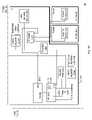
- FIG. 1illustrates a schematic representation of a data storage system, according to one embodiment of the invention.
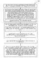
- FIG. 2illustrates a series of signals transmitted between a master device and a slave device in the data storage system of FIG. 1 during a data write procedure, according to one embodiment of the invention.
- FIG. 3illustrates a series of signals transmitted between a master device and a slave device in the data storage system of FIG. 1 during a data read procedure, according to one embodiment of the invention.
- FIG. 4illustrates a series of signals transmitted between a master device and a slave device in the data storage system of FIG. 1 during a data read procedure when the slave device is in a busy state, according to one embodiment of the invention.
- FIGS. 5A-5Dillustrates another schematic representation of a data storage system, according to one embodiment of the invention.
- FIG. 6illustrates a method for detecting a transmission error for data transferred over an I2C bus between a storage processor and a controller of the data storage system during a data read procedure.
- Embodiments of the inventionare directed to techniques for detecting the presence of errors in data transmitted between components in a data storage system using, a low speed serial protocol, such as an I2C protocol.
- the data storage systemincludes a storage processor that is configured to perform load and store operations on a storage array on behalf of external devices.
- the data storage systemalso includes a communications management device having a controller that isolates communication between the external devices when coupled to the storage array via the storage processor.
- the controllerfurther maintains a set of registers that store status and fault information associated with the data storage system and allows the storage processor to access the register via an I2C bus.
- the systemutilizes an error detection procedure.
- a checksum valueis transmitted between the controller and storage processor using the I2C bus during a register write or read procedure.
- the controller and the storage processorutilize the checksum value during error detection procedure to detect the presence or absence of data errors resulting in transmission of the data by the I2C bus.
- the use of the checksumallows error checking of data transmitted using the existing I2C protocol in the data storage system without requiring additional components (e.g., processors, etc.) to be incorporated therein.
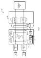
- FIG. 1illustrates an arrangement of a data storage system 20 .
- the system 20includes a data storage array 22 (e.g., a configuration of magnetic disk drives) having a storage processor 24 and a communications management device 26 coupled to the storage processor 24 .
- the storage array 22is configured to store and retrieve data for one or more external devices.
- the storage processor 24is configured to perform load and store operations on the storage array 22 on behalf of the external devices.
- the storage processor 24is also configured to provide the external devices, such as user devices 31 and service devices 33 , access to the storage array 22 .
- the storage processor 24includes a management port 28 and a service port 30 .
- a user device 31utilizes the management port 28 to load and store data relative to the storage array 22 while a service device 33 utilizes the storage port 30 to diagnose and service the storage array 22 .
- the communications management device 26is configured to isolate interaction or communication between the user and service devices 31 , 33 when coupled to the storage array 22 .
- the communications management device 26includes a first port 32 , a second port 34 , a controller 50 , and a switch 36 electrically coupled to the first and second ports 32 , 34 .
- each of the ports 32 , 34is configured as an Ethernet port, such as an RJ45 port, to allow connection of a user device or network 31 and a service device or network 33 to the communications management device 26 using a cable, such as a twisted-pair Ethernet cable.
- the switch 36such as a Broadcom 532E 10/100Base-T/TX Ethernet switch is configured to electrically couple the ports 32 , 34 of the device 26 to the ports 28 , 30 of the storage processor 24 through an electrical connection 38 .
- the communications management device 26can include a midplane connector 38 , such as a Metral series connector distributed by FCI (FCI, France), that couples to the storage processor 24 through a midplane 40 .
- the communications management device 26is configured as a field replaceable unit (FRU) that can be electrically coupled to, or decoupled from, the storage array 22 .
- FRUfield replaceable unit
- the controller 50electrically coupled to the switch 36 via interface 51 , such as a four-wire serial peripheral interface (SPI).
- the controller 50is operable to perform configuration and diagnostics operations with respect to the switch 36 .
- the controller 50is a Cypress Microcontroller model number CY8C27443, distributed by Cypress Semiconductor Corporation.
- the controller 50includes an I2C interface 49 to allow communication with components of the system 20 using an I2C protocol.
- the interface 53allows the controller 50 to communicate with the storage processor 24 over an I2C bus 56 .
- the controller 50is operable to configure a virtual local area network (VLAN) associated with the switch 36 to create various network topologies within the system 20 in order to isolate separate communications paths 42 , 44 between the ports 32 , 34 and different computerized devices or networks 31 , 33 coupled thereto.
- VLANvirtual local area network
- the controller 50includes an I2C switch (e.g., isolation module) 52 , such as a Philips PCA9546 I2C switch, distributed by Philips Semiconductors, that is configured to isolate the controller 50 from the bus 56 , such as in the event that the controller 50 holds ether the data or clock lines low.
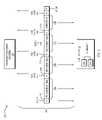
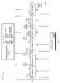
- I2C switch 52is operable to allow two controllers with the same address to communicate with the storage processor on the bus. For example, as indicated in FIGS.
- the system 20can include two distinct communications management devices 26 - 1 , 26 - 2 , each of which being coupled to two storage processors 24 - 1 , 24 - 2 via I2C busses 56 - 1 , 56 - 2 .
- the controllers 50 - 1 , 50 - 2 of the communications management devices 26 - 1 , 26 - 2have the same address (e.g., 0x90).
- Each I2C switch 52 - 1 , 52 - 2is configured to disconnect its associated controller 50 - 1 , 50 - 2 from the respective bus 56 - 1 , 56 - 2 when the other controller 50 - 1 , 50 - 2 receives communications from a master device (e.g., the storage processor 24 ). For example, when the first controller 50 - 1 receives communications from the storage processor 24 - 1 , the second I2C switch 52 - 2 disconnects the second controller 50 - 2 from the I2C bus 56 - 2 in order to minimize or prevent address conflict errors within the system 20 .
- a master devicee.g., the storage processor 24
- the controller 50maintains a set of registers 55 that store status and fault information associated with the communications management device 26 .
- the controller 50maintains a set of seven registers, each register having a corresponding register address.
- the controller 50maintains a reserved register 100 (e.g., reserved for future use), a system register 102 , a fault register 104 , first and second port status registers 106 , 108 , a manufacturing mode register 110 , a boot block revision register 112 , and a configuration revision register 114 .
- the system register 102is configured to hold information relating to the configuration, manufacturing mode, and fault status of the communications management device 26 .
- the fault register 104is configured to hold status information regarding the cause of the fault bit being set in the status register.
- the first and second port status registers 106 , 108contain information relating to port speed, link status, duplex mode, and autonegotiation settings associated with the ports 32 , 34 .
- the manufacturing mode register 110is configured to receive instructions that cause the controller 50 to activate or deactivate a fault indicator, such as an LED, associated with the communications management device 26 .
- the boot block revision register 112 and the configuration revision register 114contain the version information related to the controller 50 .
- the register 55stores information as data bytes (e.g. eight bit blocks).
- the system register 102stores data as a series of eight bits.
- the system registerincludes a reserved bit 120 , a slot identification bit 122 , manufacturing modification bits 124 , 126 , a fault state bit 128 , and a set of switch configuration mode bits 130 .
- Each bitrepresents a portion of the status information regarding the system 20 .
- the fault state bit 128is configured to indicate a fault/no fault state of the controller 50 . When the bit 128 is set to “0”, the bit indicates a no fault state of the controller 50 and when the bit 128 is set to “1”, the bit indicates a fault state of the controller 50 .
- Various devices associated with the system 20can write data to or read data from the registers 55 using a low speed serial protocol, such as an I2C protocol or bus 56 .
- the storage processor 24is configured to write data 12 to, and read data 12 from, the register 55 .
- a single storage processor 24is illustrated as communicating with the controller 50 over the I2C bus 56 , one of ordinary skill in the art will understand that any number of storage processors 24 associated with the system 20 can communicate with the controller 50 to read from or write to the registers 55 .
- the system 20can include two storage processors 24 - 1 , 24 - 2 coupled to controllers 50 - 1 , 50 - 2 via I2C busses 56 - 1 , 56 - 2 .
- the storage processor 24(e.g., master device) in the system 20 communicate with the controller 50 over the I2C bus 56 to read data from and write data to the register 55 .
- data transmission errorssuch as “bit flipping”, can occur during read or write procedures and can be undetected.
- the storage processor 24reads data from the system register 102 and the fault bit 128 is set to “0”.
- the value of the bit 128is inadvertently switched from the value “0” to the value “1”.
- the storage processor 24cannot detect that the bit value of the fault bit 128 had been changed during transmission. Therefore, the storage processor 24 detects a fault state in the controller 50 and, as a result, can execute a series of steps in an attempt to correct the non-existent fault or to prove the validity of the fault.
- the storage processor 24can implement a confirmation protocol requiring the storage processor 24 to re-read the data from the system register at least another two or three times to detect the validity of the fault. Execution of such a protocol causes the storage processor 24 to take a relatively long period of time to identify a fault.
- the system 20utilizes an error detection procedure in conjunction with the existing I2C bus 56 .
- a checksum value or signal 16is transmitted using the I2C bus 56 during a register write or read procedure, as described below with respect to FIGS. 2 and 3 .
- the controller 50 and the storage processor 24utilize the checksum value 16 during error detection procedure to detect whether the data transmitted or received via the I2C bus 56 includes errors or does not include errors as a result of the transmission.
- FIG. 2illustrates a series of signals 200 transmitted using the I2C bus 56 , between the storage processor 24 , and the controller 50 (e.g., slave device) during a data write procedure.
- the storage processor 24initially transmits a start signal or bit 202 and a controller address signal or byte 204 to the controller 50 to establish communications with the controller 50 .
- the controller 50transmits an acknowledgement bit 206 to the storage processor 24 to acknowledge reception of the address byte 204 .
- the storage processor 24then transmits a data transmission signal to the controller 50 to initiate writing of data to the controller 50 .
- the storage processortransmits a register address request signal or byte 208 that indicates the register to which the storage processor 24 is writing.
- the storage processor 24transmits a register address request byte 208 indicating that the data to be provided to the controller 50 should be written to register 0x01 (e.g., shown in Table 1 as the system register 102 ).
- the controller 50transmits, in response, an acknowledgement bit 210 .
- the storage processor 24Upon reception of the acknowledgement bit 210 , the storage processor 24 transmits a data signal or data byte 212 to the register 102 and the controller 50 provides an acknowledgement bit 214 in return.
- the storage processor 24transmits a configuration characteristic signal to the controller 50 as the data signal.
- the configuration characteristic 58indicates a particular configuration of the storage array 22 .
- the storage array 22can be configured as a storage area network (SAN) or can be configured to include a network attached storage (NAS) device, such as a gateway or a server, which forms a front-end to the storage array 22 .
- the configuration characteristic signalallows the controller 50 to detect the “type” of storage array 22 to which it is connected and allows the controller 50 to configure the switch 51 to provide certain communication pathways 42 , 44 between the first and second ports 32 , 34 of the communications management device 26 and the management and service ports 28 , 30 of the storage processor 24 based upon the storage array “type.”
- the storage processor 24transmits a checksum signal or byte 216 to the controller 50 .
- the storage processor 24calculates the checksum byte 216 prior to transmission to the controller 50 . While the checksum byte 216 can be calculated in a number of ways, in one arrangement, the storage processor 24 calculates the checksum byte 216 using the following checksum calculation algorithm.
- the storage processor 24first adds a hexadecimal value of the register address request byte 208 and a hexadecimal value of the data byte 212 .
- the storage processor 24then performs an exclusive OR, (e.g., XOR) function between the resultant sum and the hexadecimal value “0xFF” to form an intermediary result.
- the storage processor 24then adds the value “1” to the intermediary result to generate the checksum byte 216 .
- the controller 50utilizes the checksum byte 216 to engage in an error detection procedure to detect the presence of errors in the data byte 212 caused during transmission via the I2C bus 56 .
- the controller 50first adds the checksum byte 216 , the register address request byte 208 , and the data byte 212 to form a resultant sum.
- the controller 50then performs a modular division between the resultant sum and a denominator value such as the value “256” to form a validation result 230 .
- the controller 50compares the validation result 230 to a validation threshold 232 to detect errors in the data byte 212 .
- the validation threshold 232is set to the value 0x0A.
- the controller 50detects that the data byte 212 transmitted from the storage processor 24 via the I2C bus 56 has been received without errors (e.g., no flipped bits occurring in the data byte 212 ).
- the data signalis a configuration characteristic signal.
- the controller 50in response, can configure the switch 51 to provide communication pathways 42 , 44 between the first and second ports 32 , 34 of the communications management device 26 , corresponding to the storage array “type” indicated by the signal.
- the controller 50detects that the data byte 212 transmitted from the storage processor 24 via the I2C bus 56 has been received with errors (e.g., flipped bits occurring in the data byte 212 ). As a result of such detection, in one arrangement, the control 50 can generate a signal to either warn a user of the detected error or to cause the storage processor 24 to retransmit the data byte 212 to the controller 50 .
- errorse.g., flipped bits occurring in the data byte 212
- FIG. 3illustrates a series of signals 300 transmitted using the I2C bus 56 , between a master device, such as the storage processor 24 , and the controller 50 (e.g., slave device) during a data read procedure.
- FIG.6illustrates, in the storage processor 24 , a flowchart 600 showing a method for detecting a transmission error for data transferred over an I2C bus between the storage processor 24 and the a controller 50 .
- the storage processor 24initially transmits a start signal such as a start bit 302 and a controller address signal such as a controller address byte 304 to the controller 50 to establish communications with the controller 50 .
- the controller 50transmits an acknowledgement signal or bit 306 to the storage processor 24 to confirm reception of the controller address byte 204 .
- the storage processor 24then transmits a data request signal to the controller 50 using the I2C bus 56 in order to obtain data from the controller's register 55 ( FIG. 6 , element 602 ). For example, the storage processor 24 transmits, as part of the data request signal, a register address request signal or byte 308 to the controller 50 indicating the address (e.g., location) of the register from which the storage processor 24 is requesting data. For example, as illustrated, the storage processor 24 transmits a register address request byte 308 indicating that the data to be provided to the controller 50 should be read from the register having an address of 0x01 (e.g., indicated in Table 1 as the system register 102 ). The controller 50 transmits, in response, an acknowledgement bit 310 .
- a register address request signal or byte 308to the controller 50 indicating the address (e.g., location) of the register from which the storage processor 24 is requesting data.
- the storage processor 24transmits a register address request byte 308 indicating that the data to be
- the storage processor 24Upon reception of the acknowledgement bit 210 , the storage processor 24 then transmits a second start bit 311 and issues, as part of the data request signal, a second controller address signal or byte 318 to request a read from the controller 50 . The controller 50 then provides a response to the data request signal.
- the controller 50provides an acknowledgement bit 320 , along with a data response signal, to the storage processor 24 .
- the data response signalincludes a data signal 312 such as the data byte stored in the requested register, a register address reply signal or byte 350 that indicates the location or address of the register from which the data provided in the data byte 312 was taken, and a checksum signal or byte 316 .
- the checksum byte 316can be calculated in a number of ways, in one arrangement, the controller 50 calculates the checksum byte 316 using the checksum calculation algorithm described above with respect to FIG. 2 .
- the storage processor 24utilizes the data signal 312 , the register address reply signal 350 , and the checksum byte 316 to engage in an error detection procedure to detect the presence of errors in the data signal 312 56 ( FIG. 6 , element 606 ) caused during transmission via the I2C bus. For example, the storage processor 24 first adds the checksum byte 316 , the register address reply byte 350 , and the data byte 312 to form a resultant sum ( FIG. 6 , element 612 ).
- the storage processor 24then performs a modular division between the resultant sum and a denominator value, such as the value “256” to form a validation result 330 ( FIG. 6 , element 614 ).
- the storage processor 24compares the validation result 330 to a validation threshold 332 ( FIG. 6 , element 608 ) to detect the presence of errors in the data byte 312 .
- the validation threshold 332is set to the value “0x0A.” In the case where the validation result 330 is equal to the validation threshold 232 (e.g., the validation result equals “0x0A”), as indicated in FIG.
- element 610 the storage processor 24detects a first comparison result indicating that the data byte 312 read from the controller via the I2C bus 56 has been received without errors (e.g., no flipped bits occurring in the data byte 312 ).
- the storage processor 24detects a second comparison result indicating that the data byte 312 transmitted from the controller 50 via the I2C bus 56 has been received with errors (e.g., flipped bits occurring in the data byte 312 ).
- the storage processor 24can attempt to re-read the data byte 312 from the controller 50 .
- the error detection procedureallows the either the controller 50 or the storage processor 24 , respectively, to detect the presence of errors in the data transmitted via the I2C bus 56 .
- the system 20utilizes a checksum value when transmitting data with the existing I2C protocol of the system 20 .
- the recipient of the data and checksum valueeither the controller 50 or the storage processor can detect the present or absence of errors in the data.
- the data storage system 20allows error checking of data transmitted using the I2C protocol without requiring additional components (e.g., processors, caches, etc.) to be incorporated into the system 20 . Therefore, the use of the error detection procedure described, in conjunction with the I2C protocol, does not add an additional expense to the system to provide data error checking and ensure data integrity.
- the controller 50 and the storage processor 24utilize the checksum value 316 to detect whether or not data transmitted or received via the I2C bus 56 includes errors (e.g., flipped bits in the data byte) as a result of the transmission.
- the I2C bus 56can flip bits in the register address request byte 308 .
- the controller 50can receive a register address request byte 308 that requests data from a register that is different than the register originally requested by the storage processor 24 .
- the controller 50can transmit a data byte to the storage processor 24 from the “wrong” register address.
- the storage processor 24transmits the register address request byte 308 to request data from the system register 102 (Table 1) of the controller 50 .
- the resultant register address request byte 308can appear to the controller 50 as a request for data from the wrong register, such as the fault register 108 (Table 1).
- the controller 50can read the data byte 312 from a different register than the storage processor 24 actually requested and transmit the incorrect data byte 312 to the storage processor 24 .
- the storage processor 24can utilize the checksum byte 316 in an error detection procedure, the procedure would not necessarily allow the storage processor 24 to detect reception of a data byte 312 from an incorrect register address.
- the first blocks 304 , 308 , sent by the storage processor 24are write blocks that indicate, to the controller 50 , the address of the register from which the storage processor 24 wants to read. Assume, however, that the I2C bus 56 flips a bit in the register aggress signal 308 transmitted to the controller 50 . After the second start block 311 , the storage processor reads from the controller 50 to retrieve the requested data.
- the storage processorfirst receives the register address signal 350 that the controller 50 believes the storage processor 24 was requesting, followed by the data 312 and the checksum 316 . In this case, when the storage processor 24 performs the error detection procedure the checksum 316 used in the procedure will be “correct” because it was based on a “bad” register address signal 350 that was not checksum'd during the write procedure.
- the controller 50transmits the register address reply byte 350 to the storage processor 24 as part of the error detection procedure.
- the register address reply byte 350indicates the location in the register 55 from which the data provided in the data byte 312 was taken. For example, as illustrated in FIG. 3 , the register address reply byte 350 indicates that the data in the data byte 312 was taken from register address “0x01” (e.g., the system register 102 as indicated in Table 1).
- the storage processor 24compares the byte 350 with the register address request byte 308 previously sent to the controller 50 .
- the storage processor 24detects that it has received the data from the requested register address. In the case where the storage processor 24 detects that the register address reply byte 350 does not match the register address request byte 308 , the storage processor 24 detects that it has received the data byte 312 from an improper register address. Based on such detection, the storage processor 24 can attempt to re-read the data byte 312 from the controller 50 . By utilizing the register address reply byte 350 in conjunction with the register address request byte 308 , the controller 50 limits or prevents the storage processor 24 from performing unnecessary functions as a result of receiving data from a register that was not requested by the storage processor 24 .
- the controller 50is operable to configure the VLAN associated with the switch 36 to create and isolate separate communications paths 42 , 44 within the switch.
- the controller 50enters a busy state.
- the controller 50can service write requests transmitted from the storage processor 24 in the system 20 , in one arrangement, the controller 50 cannot service read requests. Therefore, in order to allow the controller 50 to delay responding to the read request from the storage processor while maintaining communications with the storage processor 24 , the controller 50 engages in a busy read transaction with the storage processor 24 .
- FIG. 4illustrates the use of the busy read transaction during a data read procedure performed by the storage processor 24 .
- the storage processor 24transmits the controller address byte 304 , the register address request byte 308 , and a reissued controller address byte 318 to the controller 50 .
- the controller 50transmits a busy condition indicator or byte 402 to the storage processor 24 .
- the controller 50transmits the busy condition byte 402 in place of the register address reply byte 350 , shown in FIG. 3 .
- the use of the busy condition byte 402limits or prevents the controller 50 from transmitting invalid data, such as data taken from an unrequested register, to the storage processor 24 while the controller 50 is in the process of configuring the switch 36 .
- the storage processor 24transmits an acknowledgement bit 403 to the controller 50 .
- the controller 50transmits a placeholder byte 404 to the storage processor 34 ( FIG. 6 , element 618 ).
- the placeholder byte 404includes a sequence of signals, such as a three byte sequence that indicates to the storage processor 24 that the controller 50 is busy.
- the placeholder byte 404also indicates a time duration after which the controller 50 will be available. For example, the placeholder byte 404 can indicate the controller's availability after the expiration of some duration of time, such as 30 milliseconds. Based upon the placeholder byte 404 , the storage processor 24 can then retransmit the request to read data from the controller 50 ( FIG. 6 , element 620 ).
- the system 20uses a checksum signal to allow the controller 50 and storage processor 24 to detect errors in data transmitted between the devices 50 , 24 over the I2C bus 56 .
- a checksum signalto allow the controller 50 and storage processor 24 to detect errors in data transmitted between the devices 50 , 24 over the I2C bus 56 .
- error detectioncan be utilized in conjunction with the I2C protocol.
- paritycan be utilized with the I2C protocol as part of the error checking procedure.
- the storage processor 24is described as performing block read and write operations. As such, the storage processor operates as the master device. Such description is by way of example only.
- the term “master”is used to represent the storage processor, 24 , power source 25 (e.g., processor associated with the power source 25 ), or any other element 27 , such as one or more cache cards 27 - 1 , 27 - 2 , shown in FIGS. 5A-5D , that communicate with the controllers 50 - 1 , 50 - 2 using the I2C buses 56 - 1 , 56 - 2 , respectively.
Landscapes
- Engineering & Computer Science (AREA)
- Computer Networks & Wireless Communication (AREA)
- Signal Processing (AREA)
- Debugging And Monitoring (AREA)
- Detection And Correction Of Errors (AREA)
Abstract
Description
| TABLE 1 |
| Register Map |
| REGISTER | |
| ADDRESS | |
| REGISTER | (Hex Number) |
| 100 | Reserved | 0x00 |
| 102 | System Register (Read/Write) | 0x01 |
| 104 | Fault Register (Read/Write) | 0x02 |
| 106 | Port Status Register A (Read Only) | 0x03 |
| 108 | Port Status Register B (Read Only) | 0x04 |
| 110 | Manufacturing Mode Register (Write Only | 0x05 |
| 112 | Boot Block Revision Register (Read Only) | 0x06 |
| 114 | Configuration Revision Register (Read Only) | 0x07 |
| TABLE 2 |
| System Register Bits Map |
| SYSTEM REGISTER | ||
| BITS | DESCRIPTION | |
| 120 | 7 | Reserved |
| 122 | 6 | Slot ID |
| 124 | 5 | External Enabled Manufacturing Mode |
| 126 | 4 | Software Enable Manufacturing Mode |
| 128 | 3 | Fault State |
| 130 | 2:0 | Switch Configuration Mode |
Claims (18)
Priority Applications (1)
| Application Number | Priority Date | Filing Date | Title |
|---|---|---|---|
| US11/394,919US7502992B2 (en) | 2006-03-31 | 2006-03-31 | Method and apparatus for detecting presence of errors in data transmitted between components in a data storage system using an I2C protocol |
Applications Claiming Priority (1)
| Application Number | Priority Date | Filing Date | Title |
|---|---|---|---|
| US11/394,919US7502992B2 (en) | 2006-03-31 | 2006-03-31 | Method and apparatus for detecting presence of errors in data transmitted between components in a data storage system using an I2C protocol |
Publications (2)
| Publication Number | Publication Date |
|---|---|
| US20070234136A1 US20070234136A1 (en) | 2007-10-04 |
| US7502992B2true US7502992B2 (en) | 2009-03-10 |
Family
ID=38560931
Family Applications (1)
| Application Number | Title | Priority Date | Filing Date |
|---|---|---|---|
| US11/394,919Active2027-03-02US7502992B2 (en) | 2006-03-31 | 2006-03-31 | Method and apparatus for detecting presence of errors in data transmitted between components in a data storage system using an I2C protocol |
Country Status (1)
| Country | Link |
|---|---|
| US (1) | US7502992B2 (en) |
Cited By (1)
| Publication number | Priority date | Publication date | Assignee | Title |
|---|---|---|---|---|
| US10445013B2 (en) | 2016-09-23 | 2019-10-15 | EMC IP Holding Company LLC | Method and device for storing data |
Families Citing this family (16)
| Publication number | Priority date | Publication date | Assignee | Title |
|---|---|---|---|---|
| JP2007164765A (en)* | 2005-11-15 | 2007-06-28 | Matsushita Electric Ind Co Ltd | IIC bus communication system, slave device, and IIC bus communication control method |
| US7533191B2 (en)* | 2006-06-30 | 2009-05-12 | Intel Corporation | Methods and arrangements for devices to share a common address on a bus |
| US20090138638A1 (en) | 2007-11-27 | 2009-05-28 | Microsoft Corporation | Serial Peripheral Interface for a Transceiver Integrated Circuit |
| JP4644720B2 (en)* | 2008-03-10 | 2011-03-02 | 富士通株式会社 | Control method, information processing apparatus, and storage system |
| US10353837B2 (en) | 2013-09-09 | 2019-07-16 | Qualcomm Incorporated | Method and apparatus to enable multiple masters to operate in a single master bus architecture |
| US9690725B2 (en) | 2014-01-14 | 2017-06-27 | Qualcomm Incorporated | Camera control interface extension with in-band interrupt |
| US9996488B2 (en) | 2013-09-09 | 2018-06-12 | Qualcomm Incorporated | I3C high data rate (HDR) always-on image sensor 8-bit operation indicator and buffer over threshold indicator |
| KR20160070171A (en)* | 2013-10-09 | 2016-06-17 | 퀄컴 인코포레이티드 | ERROR DETECTION CAPABILITY OVER CCIe PROTOCOL |
| US9684624B2 (en) | 2014-01-14 | 2017-06-20 | Qualcomm Incorporated | Receive clock calibration for a serial bus |
| US20150248373A1 (en)* | 2014-02-28 | 2015-09-03 | Qualcomm Incorporated | Bit allocation over a shared bus to facilitate an error detection optimization |
| TWI620066B (en)* | 2015-10-30 | 2018-04-01 | 神雲科技股份有限公司 | Communication method of inter-integrated circuit and expander device using the same |
| CN107678879A (en)* | 2016-08-01 | 2018-02-09 | 北京同方微电子有限公司 | A kind of apparatus and method verified in real time for bus and memory cell data block |
| US10783109B2 (en)* | 2018-10-24 | 2020-09-22 | Dell Products, L.P. | Device management messaging protocol proxy |
| CN111159057A (en)* | 2019-12-11 | 2020-05-15 | 江西洪都航空工业集团有限责任公司 | System and method for recording accumulated power-on times of task machine under battery-free condition |
| EP3869742B1 (en)* | 2020-02-20 | 2023-06-07 | Nxp B.V. | Network node |
| CN112463662B (en)* | 2020-12-16 | 2024-04-05 | 福州创实讯联信息技术有限公司 | Method and terminal for user mode control of I2C equipment |
Citations (11)
| Publication number | Priority date | Publication date | Assignee | Title |
|---|---|---|---|---|
| US5283792A (en) | 1990-10-19 | 1994-02-01 | Benchmarq Microelectronics, Inc. | Power up/power down controller and power fail detector for processor |
| US5774640A (en) | 1991-10-21 | 1998-06-30 | Tandem Computers Incorporated | Method and apparatus for providing a fault tolerant network interface controller |
| US5935261A (en)* | 1997-06-05 | 1999-08-10 | International Business Machines Corporation | Method and apparatus for detecting handling damage in a disk drive |
| US6633905B1 (en) | 1998-09-22 | 2003-10-14 | Avocent Huntsville Corporation | System and method for accessing and operating personal computers remotely |
| US6678639B2 (en) | 2000-08-04 | 2004-01-13 | Sun Microsystems, Inc. | Automated problem identification system |
| US6681282B1 (en) | 2000-08-31 | 2004-01-20 | Hewlett-Packard Development Company, L.P. | Online control of a multiprocessor computer system |
| US6728908B1 (en) | 1999-11-18 | 2004-04-27 | California Institute Of Technology | I2C bus protocol controller with fault tolerance |
| US6873268B2 (en) | 2000-01-21 | 2005-03-29 | Medtronic Minimed, Inc. | Microprocessor controlled ambulatory medical apparatus with hand held communication device |
| US6910148B1 (en) | 2000-12-07 | 2005-06-21 | Nokia, Inc. | Router and routing protocol redundancy |
| US20050154841A1 (en)* | 2001-05-08 | 2005-07-14 | Gautham Sastri | Data storage system for a multi-client network and method of managing such system |
| US7039737B1 (en) | 2003-12-12 | 2006-05-02 | Emc Corporation | Method and apparatus for resource arbitration |
- 2006
- 2006-03-31USUS11/394,919patent/US7502992B2/enactiveActive
Patent Citations (11)
| Publication number | Priority date | Publication date | Assignee | Title |
|---|---|---|---|---|
| US5283792A (en) | 1990-10-19 | 1994-02-01 | Benchmarq Microelectronics, Inc. | Power up/power down controller and power fail detector for processor |
| US5774640A (en) | 1991-10-21 | 1998-06-30 | Tandem Computers Incorporated | Method and apparatus for providing a fault tolerant network interface controller |
| US5935261A (en)* | 1997-06-05 | 1999-08-10 | International Business Machines Corporation | Method and apparatus for detecting handling damage in a disk drive |
| US6633905B1 (en) | 1998-09-22 | 2003-10-14 | Avocent Huntsville Corporation | System and method for accessing and operating personal computers remotely |
| US6728908B1 (en) | 1999-11-18 | 2004-04-27 | California Institute Of Technology | I2C bus protocol controller with fault tolerance |
| US6873268B2 (en) | 2000-01-21 | 2005-03-29 | Medtronic Minimed, Inc. | Microprocessor controlled ambulatory medical apparatus with hand held communication device |
| US6678639B2 (en) | 2000-08-04 | 2004-01-13 | Sun Microsystems, Inc. | Automated problem identification system |
| US6681282B1 (en) | 2000-08-31 | 2004-01-20 | Hewlett-Packard Development Company, L.P. | Online control of a multiprocessor computer system |
| US6910148B1 (en) | 2000-12-07 | 2005-06-21 | Nokia, Inc. | Router and routing protocol redundancy |
| US20050154841A1 (en)* | 2001-05-08 | 2005-07-14 | Gautham Sastri | Data storage system for a multi-client network and method of managing such system |
| US7039737B1 (en) | 2003-12-12 | 2006-05-02 | Emc Corporation | Method and apparatus for resource arbitration |
Non-Patent Citations (2)
| Title |
|---|
| Data Sheet: EMC Clariion CX Series, EMC Corporation, 2004, 8 pages. |
| http://www.storagesearch.com/fchub.html, "The Shift to NAS Gateways," visited Aug. 17, 2006, 4 pages. |
Cited By (1)
| Publication number | Priority date | Publication date | Assignee | Title |
|---|---|---|---|---|
| US10445013B2 (en) | 2016-09-23 | 2019-10-15 | EMC IP Holding Company LLC | Method and device for storing data |
Also Published As
| Publication number | Publication date |
|---|---|
| US20070234136A1 (en) | 2007-10-04 |
Similar Documents
| Publication | Publication Date | Title |
|---|---|---|
| US7502992B2 (en) | Method and apparatus for detecting presence of errors in data transmitted between components in a data storage system using an I2C protocol | |
| Peña et al. | Uart: A hardware communication protocol understanding universal asynchronous receiver/transmitter | |
| EP1921801B1 (en) | Method and network for forwarding messages with priority-based arbitration | |
| US8665882B2 (en) | Serialized enforced authenticated controller area network | |
| JP2545508B2 (en) | Method of operating data processing device for vehicle and data processing device | |
| US5838899A (en) | Digital data processing methods and apparatus for fault isolation | |
| US5371897A (en) | Method for requesting identification of a neighbor node in a data processing I/O system | |
| US6425009B1 (en) | Monitoring redundant control buses to provide a high availability local area network for a telecommunications device | |
| US7574540B2 (en) | Managing management controller communications | |
| US7788523B2 (en) | Method and apparatus for relating device name to physical location of device on a network | |
| US5574865A (en) | System for data transfer protection during module connection/disconnection onto live bus | |
| US11463198B2 (en) | Security module for a serial communications device | |
| US8089903B2 (en) | Method and apparatus for providing a logical separation of a customer device and a service device connected to a data storage system | |
| CN1758622A (en) | Heterogeneous multi-bus data transmission method between information processing device | |
| US7685442B2 (en) | Method and systems for a radiation tolerant bus interface circuit | |
| JP2007013980A (en) | Redundant 3-wire communication system and method | |
| JP2001337869A (en) | Data storage system with message network including independent data transmitting division, a plurality of directors on common printed-circuit board, and redundant switching network | |
| JP6134720B2 (en) | Connection method | |
| US8050176B2 (en) | Methods and systems for a data processing system having radiation tolerant bus | |
| CN101189593A (en) | Method for transferring redundant data during address transfer on a multiplexed address/data bus | |
| US7712004B1 (en) | Method of and system for error checking in a data storage system | |
| US7440398B2 (en) | Fault tolerant communication apparatus | |
| US7009969B1 (en) | Local area network and message packet for a telecommunications device | |
| JP2001331385A (en) | Data memory system having message network provided with plural directors on separated data transfer part and common circuit board | |
| Maryanka et al. | The Vehicle Power Line as a Redundant Channel for CAN Communication |
Legal Events
| Date | Code | Title | Description |
|---|---|---|---|
| AS | Assignment | Owner name:EMC CORPORATION, MASSACHUSETTS Free format text:ASSIGNMENT OF ASSIGNORS INTEREST;ASSIGNORS:LEEF, PHILLIP;SULLIVAN, DOUGLAS;STRICKLAND, STEPHEN;AND OTHERS;REEL/FRAME:017755/0827 Effective date:20060330 | |
| STCF | Information on status: patent grant | Free format text:PATENTED CASE | |
| CC | Certificate of correction | ||
| CC | Certificate of correction | ||
| FEPP | Fee payment procedure | Free format text:PAYOR NUMBER ASSIGNED (ORIGINAL EVENT CODE: ASPN); ENTITY STATUS OF PATENT OWNER: LARGE ENTITY | |
| FPAY | Fee payment | Year of fee payment:4 | |
| FPAY | Fee payment | Year of fee payment:8 | |
| AS | Assignment | Owner name:THE BANK OF NEW YORK MELLON TRUST COMPANY, N.A., AS NOTES COLLATERAL AGENT, TEXAS Free format text:SECURITY AGREEMENT;ASSIGNORS:ASAP SOFTWARE EXPRESS, INC.;AVENTAIL LLC;CREDANT TECHNOLOGIES, INC.;AND OTHERS;REEL/FRAME:040136/0001 Effective date:20160907 Owner name:CREDIT SUISSE AG, CAYMAN ISLANDS BRANCH, AS COLLATERAL AGENT, NORTH CAROLINA Free format text:SECURITY AGREEMENT;ASSIGNORS:ASAP SOFTWARE EXPRESS, INC.;AVENTAIL LLC;CREDANT TECHNOLOGIES, INC.;AND OTHERS;REEL/FRAME:040134/0001 Effective date:20160907 Owner name:CREDIT SUISSE AG, CAYMAN ISLANDS BRANCH, AS COLLAT Free format text:SECURITY AGREEMENT;ASSIGNORS:ASAP SOFTWARE EXPRESS, INC.;AVENTAIL LLC;CREDANT TECHNOLOGIES, INC.;AND OTHERS;REEL/FRAME:040134/0001 Effective date:20160907 Owner name:THE BANK OF NEW YORK MELLON TRUST COMPANY, N.A., A Free format text:SECURITY AGREEMENT;ASSIGNORS:ASAP SOFTWARE EXPRESS, INC.;AVENTAIL LLC;CREDANT TECHNOLOGIES, INC.;AND OTHERS;REEL/FRAME:040136/0001 Effective date:20160907 | |
| AS | Assignment | Owner name:EMC IP HOLDING COMPANY LLC, MASSACHUSETTS Free format text:ASSIGNMENT OF ASSIGNORS INTEREST;ASSIGNOR:EMC CORPORATION;REEL/FRAME:040203/0001 Effective date:20160906 | |
| AS | Assignment | Owner name:THE BANK OF NEW YORK MELLON TRUST COMPANY, N.A., T Free format text:SECURITY AGREEMENT;ASSIGNORS:CREDANT TECHNOLOGIES, INC.;DELL INTERNATIONAL L.L.C.;DELL MARKETING L.P.;AND OTHERS;REEL/FRAME:049452/0223 Effective date:20190320 Owner name:THE BANK OF NEW YORK MELLON TRUST COMPANY, N.A., TEXAS Free format text:SECURITY AGREEMENT;ASSIGNORS:CREDANT TECHNOLOGIES, INC.;DELL INTERNATIONAL L.L.C.;DELL MARKETING L.P.;AND OTHERS;REEL/FRAME:049452/0223 Effective date:20190320 | |
| AS | Assignment | Owner name:THE BANK OF NEW YORK MELLON TRUST COMPANY, N.A., TEXAS Free format text:SECURITY AGREEMENT;ASSIGNORS:CREDANT TECHNOLOGIES INC.;DELL INTERNATIONAL L.L.C.;DELL MARKETING L.P.;AND OTHERS;REEL/FRAME:053546/0001 Effective date:20200409 | |
| MAFP | Maintenance fee payment | Free format text:PAYMENT OF MAINTENANCE FEE, 12TH YEAR, LARGE ENTITY (ORIGINAL EVENT CODE: M1553); ENTITY STATUS OF PATENT OWNER: LARGE ENTITY Year of fee payment:12 | |
| AS | Assignment | Owner name:WYSE TECHNOLOGY L.L.C., CALIFORNIA Free format text:RELEASE BY SECURED PARTY;ASSIGNOR:CREDIT SUISSE AG, CAYMAN ISLANDS BRANCH;REEL/FRAME:058216/0001 Effective date:20211101 Owner name:SCALEIO LLC, MASSACHUSETTS Free format text:RELEASE BY SECURED PARTY;ASSIGNOR:CREDIT SUISSE AG, CAYMAN ISLANDS BRANCH;REEL/FRAME:058216/0001 Effective date:20211101 Owner name:MOZY, INC., WASHINGTON Free format text:RELEASE BY SECURED PARTY;ASSIGNOR:CREDIT SUISSE AG, CAYMAN ISLANDS BRANCH;REEL/FRAME:058216/0001 Effective date:20211101 Owner name:MAGINATICS LLC, CALIFORNIA Free format text:RELEASE BY SECURED PARTY;ASSIGNOR:CREDIT SUISSE AG, CAYMAN ISLANDS BRANCH;REEL/FRAME:058216/0001 Effective date:20211101 Owner name:FORCE10 NETWORKS, INC., CALIFORNIA Free format text:RELEASE BY SECURED PARTY;ASSIGNOR:CREDIT SUISSE AG, CAYMAN ISLANDS BRANCH;REEL/FRAME:058216/0001 Effective date:20211101 Owner name:EMC IP HOLDING COMPANY LLC, TEXAS Free format text:RELEASE BY SECURED PARTY;ASSIGNOR:CREDIT SUISSE AG, CAYMAN ISLANDS BRANCH;REEL/FRAME:058216/0001 Effective date:20211101 Owner name:EMC CORPORATION, MASSACHUSETTS Free format text:RELEASE BY SECURED PARTY;ASSIGNOR:CREDIT SUISSE AG, CAYMAN ISLANDS BRANCH;REEL/FRAME:058216/0001 Effective date:20211101 Owner name:DELL SYSTEMS CORPORATION, TEXAS Free format text:RELEASE BY SECURED PARTY;ASSIGNOR:CREDIT SUISSE AG, CAYMAN ISLANDS BRANCH;REEL/FRAME:058216/0001 Effective date:20211101 Owner name:DELL SOFTWARE INC., CALIFORNIA Free format text:RELEASE BY SECURED PARTY;ASSIGNOR:CREDIT SUISSE AG, CAYMAN ISLANDS BRANCH;REEL/FRAME:058216/0001 Effective date:20211101 Owner name:DELL PRODUCTS L.P., TEXAS Free format text:RELEASE BY SECURED PARTY;ASSIGNOR:CREDIT SUISSE AG, CAYMAN ISLANDS BRANCH;REEL/FRAME:058216/0001 Effective date:20211101 Owner name:DELL MARKETING L.P., TEXAS Free format text:RELEASE BY SECURED PARTY;ASSIGNOR:CREDIT SUISSE AG, CAYMAN ISLANDS BRANCH;REEL/FRAME:058216/0001 Effective date:20211101 Owner name:DELL INTERNATIONAL, L.L.C., TEXAS Free format text:RELEASE BY SECURED PARTY;ASSIGNOR:CREDIT SUISSE AG, CAYMAN ISLANDS BRANCH;REEL/FRAME:058216/0001 Effective date:20211101 Owner name:DELL USA L.P., TEXAS Free format text:RELEASE BY SECURED PARTY;ASSIGNOR:CREDIT SUISSE AG, CAYMAN ISLANDS BRANCH;REEL/FRAME:058216/0001 Effective date:20211101 Owner name:CREDANT TECHNOLOGIES, INC., TEXAS Free format text:RELEASE BY SECURED PARTY;ASSIGNOR:CREDIT SUISSE AG, CAYMAN ISLANDS BRANCH;REEL/FRAME:058216/0001 Effective date:20211101 Owner name:AVENTAIL LLC, CALIFORNIA Free format text:RELEASE BY SECURED PARTY;ASSIGNOR:CREDIT SUISSE AG, CAYMAN ISLANDS BRANCH;REEL/FRAME:058216/0001 Effective date:20211101 Owner name:ASAP SOFTWARE EXPRESS, INC., ILLINOIS Free format text:RELEASE BY SECURED PARTY;ASSIGNOR:CREDIT SUISSE AG, CAYMAN ISLANDS BRANCH;REEL/FRAME:058216/0001 Effective date:20211101 | |
| AS | Assignment | Owner name:SCALEIO LLC, MASSACHUSETTS Free format text:RELEASE OF SECURITY INTEREST IN PATENTS PREVIOUSLY RECORDED AT REEL/FRAME (040136/0001);ASSIGNOR:THE BANK OF NEW YORK MELLON TRUST COMPANY, N.A., AS NOTES COLLATERAL AGENT;REEL/FRAME:061324/0001 Effective date:20220329 Owner name:EMC IP HOLDING COMPANY LLC (ON BEHALF OF ITSELF AND AS SUCCESSOR-IN-INTEREST TO MOZY, INC.), TEXAS Free format text:RELEASE OF SECURITY INTEREST IN PATENTS PREVIOUSLY RECORDED AT REEL/FRAME (040136/0001);ASSIGNOR:THE BANK OF NEW YORK MELLON TRUST COMPANY, N.A., AS NOTES COLLATERAL AGENT;REEL/FRAME:061324/0001 Effective date:20220329 Owner name:EMC CORPORATION (ON BEHALF OF ITSELF AND AS SUCCESSOR-IN-INTEREST TO MAGINATICS LLC), MASSACHUSETTS Free format text:RELEASE OF SECURITY INTEREST IN PATENTS PREVIOUSLY RECORDED AT REEL/FRAME (040136/0001);ASSIGNOR:THE BANK OF NEW YORK MELLON TRUST COMPANY, N.A., AS NOTES COLLATERAL AGENT;REEL/FRAME:061324/0001 Effective date:20220329 Owner name:DELL MARKETING CORPORATION (SUCCESSOR-IN-INTEREST TO FORCE10 NETWORKS, INC. AND WYSE TECHNOLOGY L.L.C.), TEXAS Free format text:RELEASE OF SECURITY INTEREST IN PATENTS PREVIOUSLY RECORDED AT REEL/FRAME (040136/0001);ASSIGNOR:THE BANK OF NEW YORK MELLON TRUST COMPANY, N.A., AS NOTES COLLATERAL AGENT;REEL/FRAME:061324/0001 Effective date:20220329 Owner name:DELL PRODUCTS L.P., TEXAS Free format text:RELEASE OF SECURITY INTEREST IN PATENTS PREVIOUSLY RECORDED AT REEL/FRAME (040136/0001);ASSIGNOR:THE BANK OF NEW YORK MELLON TRUST COMPANY, N.A., AS NOTES COLLATERAL AGENT;REEL/FRAME:061324/0001 Effective date:20220329 Owner name:DELL INTERNATIONAL L.L.C., TEXAS Free format text:RELEASE OF SECURITY INTEREST IN PATENTS PREVIOUSLY RECORDED AT REEL/FRAME (040136/0001);ASSIGNOR:THE BANK OF NEW YORK MELLON TRUST COMPANY, N.A., AS NOTES COLLATERAL AGENT;REEL/FRAME:061324/0001 Effective date:20220329 Owner name:DELL USA L.P., TEXAS Free format text:RELEASE OF SECURITY INTEREST IN PATENTS PREVIOUSLY RECORDED AT REEL/FRAME (040136/0001);ASSIGNOR:THE BANK OF NEW YORK MELLON TRUST COMPANY, N.A., AS NOTES COLLATERAL AGENT;REEL/FRAME:061324/0001 Effective date:20220329 Owner name:DELL MARKETING L.P. (ON BEHALF OF ITSELF AND AS SUCCESSOR-IN-INTEREST TO CREDANT TECHNOLOGIES, INC.), TEXAS Free format text:RELEASE OF SECURITY INTEREST IN PATENTS PREVIOUSLY RECORDED AT REEL/FRAME (040136/0001);ASSIGNOR:THE BANK OF NEW YORK MELLON TRUST COMPANY, N.A., AS NOTES COLLATERAL AGENT;REEL/FRAME:061324/0001 Effective date:20220329 Owner name:DELL MARKETING CORPORATION (SUCCESSOR-IN-INTEREST TO ASAP SOFTWARE EXPRESS, INC.), TEXAS Free format text:RELEASE OF SECURITY INTEREST IN PATENTS PREVIOUSLY RECORDED AT REEL/FRAME (040136/0001);ASSIGNOR:THE BANK OF NEW YORK MELLON TRUST COMPANY, N.A., AS NOTES COLLATERAL AGENT;REEL/FRAME:061324/0001 Effective date:20220329 | |
| AS | Assignment | Owner name:SCALEIO LLC, MASSACHUSETTS Free format text:RELEASE OF SECURITY INTEREST IN PATENTS PREVIOUSLY RECORDED AT REEL/FRAME (045455/0001);ASSIGNOR:THE BANK OF NEW YORK MELLON TRUST COMPANY, N.A., AS NOTES COLLATERAL AGENT;REEL/FRAME:061753/0001 Effective date:20220329 Owner name:EMC IP HOLDING COMPANY LLC (ON BEHALF OF ITSELF AND AS SUCCESSOR-IN-INTEREST TO MOZY, INC.), TEXAS Free format text:RELEASE OF SECURITY INTEREST IN PATENTS PREVIOUSLY RECORDED AT REEL/FRAME (045455/0001);ASSIGNOR:THE BANK OF NEW YORK MELLON TRUST COMPANY, N.A., AS NOTES COLLATERAL AGENT;REEL/FRAME:061753/0001 Effective date:20220329 Owner name:EMC CORPORATION (ON BEHALF OF ITSELF AND AS SUCCESSOR-IN-INTEREST TO MAGINATICS LLC), MASSACHUSETTS Free format text:RELEASE OF SECURITY INTEREST IN PATENTS PREVIOUSLY RECORDED AT REEL/FRAME (045455/0001);ASSIGNOR:THE BANK OF NEW YORK MELLON TRUST COMPANY, N.A., AS NOTES COLLATERAL AGENT;REEL/FRAME:061753/0001 Effective date:20220329 Owner name:DELL MARKETING CORPORATION (SUCCESSOR-IN-INTEREST TO FORCE10 NETWORKS, INC. AND WYSE TECHNOLOGY L.L.C.), TEXAS Free format text:RELEASE OF SECURITY INTEREST IN PATENTS PREVIOUSLY RECORDED AT REEL/FRAME (045455/0001);ASSIGNOR:THE BANK OF NEW YORK MELLON TRUST COMPANY, N.A., AS NOTES COLLATERAL AGENT;REEL/FRAME:061753/0001 Effective date:20220329 Owner name:DELL PRODUCTS L.P., TEXAS Free format text:RELEASE OF SECURITY INTEREST IN PATENTS PREVIOUSLY RECORDED AT REEL/FRAME (045455/0001);ASSIGNOR:THE BANK OF NEW YORK MELLON TRUST COMPANY, N.A., AS NOTES COLLATERAL AGENT;REEL/FRAME:061753/0001 Effective date:20220329 Owner name:DELL INTERNATIONAL L.L.C., TEXAS Free format text:RELEASE OF SECURITY INTEREST IN PATENTS PREVIOUSLY RECORDED AT REEL/FRAME (045455/0001);ASSIGNOR:THE BANK OF NEW YORK MELLON TRUST COMPANY, N.A., AS NOTES COLLATERAL AGENT;REEL/FRAME:061753/0001 Effective date:20220329 Owner name:DELL USA L.P., TEXAS Free format text:RELEASE OF SECURITY INTEREST IN PATENTS PREVIOUSLY RECORDED AT REEL/FRAME (045455/0001);ASSIGNOR:THE BANK OF NEW YORK MELLON TRUST COMPANY, N.A., AS NOTES COLLATERAL AGENT;REEL/FRAME:061753/0001 Effective date:20220329 Owner name:DELL MARKETING L.P. (ON BEHALF OF ITSELF AND AS SUCCESSOR-IN-INTEREST TO CREDANT TECHNOLOGIES, INC.), TEXAS Free format text:RELEASE OF SECURITY INTEREST IN PATENTS PREVIOUSLY RECORDED AT REEL/FRAME (045455/0001);ASSIGNOR:THE BANK OF NEW YORK MELLON TRUST COMPANY, N.A., AS NOTES COLLATERAL AGENT;REEL/FRAME:061753/0001 Effective date:20220329 Owner name:DELL MARKETING CORPORATION (SUCCESSOR-IN-INTEREST TO ASAP SOFTWARE EXPRESS, INC.), TEXAS Free format text:RELEASE OF SECURITY INTEREST IN PATENTS PREVIOUSLY RECORDED AT REEL/FRAME (045455/0001);ASSIGNOR:THE BANK OF NEW YORK MELLON TRUST COMPANY, N.A., AS NOTES COLLATERAL AGENT;REEL/FRAME:061753/0001 Effective date:20220329 | |
| AS | Assignment | Owner name:DELL MARKETING L.P. (ON BEHALF OF ITSELF AND AS SUCCESSOR-IN-INTEREST TO CREDANT TECHNOLOGIES, INC.), TEXAS Free format text:RELEASE OF SECURITY INTEREST IN PATENTS PREVIOUSLY RECORDED AT REEL/FRAME (053546/0001);ASSIGNOR:THE BANK OF NEW YORK MELLON TRUST COMPANY, N.A., AS NOTES COLLATERAL AGENT;REEL/FRAME:071642/0001 Effective date:20220329 Owner name:DELL INTERNATIONAL L.L.C., TEXAS Free format text:RELEASE OF SECURITY INTEREST IN PATENTS PREVIOUSLY RECORDED AT REEL/FRAME (053546/0001);ASSIGNOR:THE BANK OF NEW YORK MELLON TRUST COMPANY, N.A., AS NOTES COLLATERAL AGENT;REEL/FRAME:071642/0001 Effective date:20220329 Owner name:DELL PRODUCTS L.P., TEXAS Free format text:RELEASE OF SECURITY INTEREST IN PATENTS PREVIOUSLY RECORDED AT REEL/FRAME (053546/0001);ASSIGNOR:THE BANK OF NEW YORK MELLON TRUST COMPANY, N.A., AS NOTES COLLATERAL AGENT;REEL/FRAME:071642/0001 Effective date:20220329 Owner name:DELL USA L.P., TEXAS Free format text:RELEASE OF SECURITY INTEREST IN PATENTS PREVIOUSLY RECORDED AT REEL/FRAME (053546/0001);ASSIGNOR:THE BANK OF NEW YORK MELLON TRUST COMPANY, N.A., AS NOTES COLLATERAL AGENT;REEL/FRAME:071642/0001 Effective date:20220329 Owner name:EMC CORPORATION, MASSACHUSETTS Free format text:RELEASE OF SECURITY INTEREST IN PATENTS PREVIOUSLY RECORDED AT REEL/FRAME (053546/0001);ASSIGNOR:THE BANK OF NEW YORK MELLON TRUST COMPANY, N.A., AS NOTES COLLATERAL AGENT;REEL/FRAME:071642/0001 Effective date:20220329 Owner name:DELL MARKETING CORPORATION (SUCCESSOR-IN-INTEREST TO FORCE10 NETWORKS, INC. AND WYSE TECHNOLOGY L.L.C.), TEXAS Free format text:RELEASE OF SECURITY INTEREST IN PATENTS PREVIOUSLY RECORDED AT REEL/FRAME (053546/0001);ASSIGNOR:THE BANK OF NEW YORK MELLON TRUST COMPANY, N.A., AS NOTES COLLATERAL AGENT;REEL/FRAME:071642/0001 Effective date:20220329 Owner name:EMC IP HOLDING COMPANY LLC, TEXAS Free format text:RELEASE OF SECURITY INTEREST IN PATENTS PREVIOUSLY RECORDED AT REEL/FRAME (053546/0001);ASSIGNOR:THE BANK OF NEW YORK MELLON TRUST COMPANY, N.A., AS NOTES COLLATERAL AGENT;REEL/FRAME:071642/0001 Effective date:20220329 |