US7498999B2 - Circuit board having a peripheral antenna apparatus with selectable antenna elements and selectable phase shifting - Google Patents
Circuit board having a peripheral antenna apparatus with selectable antenna elements and selectable phase shiftingDownload PDFInfo
- Publication number
- US7498999B2 US7498999B2US11/265,751US26575105AUS7498999B2US 7498999 B2US7498999 B2US 7498999B2US 26575105 AUS26575105 AUS 26575105AUS 7498999 B2US7498999 B2US 7498999B2
- Authority
- US
- United States
- Prior art keywords
- path
- signal
- switch
- delay
- input port
- Prior art date
- Legal status (The legal status is an assumption and is not a legal conclusion. Google has not performed a legal analysis and makes no representation as to the accuracy of the status listed.)
- Expired - Fee Related, expires
Links
Images


Classifications
- H—ELECTRICITY
- H01—ELECTRIC ELEMENTS
- H01P—WAVEGUIDES; RESONATORS, LINES, OR OTHER DEVICES OF THE WAVEGUIDE TYPE
- H01P1/00—Auxiliary devices
- H01P1/18—Phase-shifters
- H01P1/185—Phase-shifters using a diode or a gas filled discharge tube
Definitions
- the present inventionrelates generally to wireless communications, and more particularly to a circuit board having a peripheral antenna apparatus with selectable antenna elements and selectable phase shifting.
- an access pointi.e., base station
- communicates data with one or more remote receiving nodese.g., a network interface card
- the wireless linkmay be susceptible to interference from other access points, other radio transmitting devices, changes or disturbances in the wireless link environment between the access point and the remote receiving node, and so on.
- the interferencemay be such to degrade the wireless link, for example by forcing communication at a lower data rate, or may be sufficiently strong to completely disrupt the wireless link.
- a common configuration for the access pointcomprises a data source coupled via a switching network to two or more physically separated omnidirectional antennas.
- the access pointmay select one of the omnidirectional antennas by which to maintain the wireless link. Because of the separation between the omnidirectional antennas, each antenna experiences a different signal environment, and each antenna contributes a different interference level to the wireless link.
- the switching networkcouples the data source to whichever of the omnidirectional antennas experiences the least interference in the wireless link.
- each omnidirectional antennacomprises a separate unit of manufacture with respect to the access point, thus requiring extra manufacturing steps to include the omnidirectional antennas in the access point.
- the omnidirectional antennatypically comprises an upright wand attached to a housing of the access point. The wand typically comprises a rod exposed outside of the housing, and may be subject to breakage or damage.
- Typical omnidirectional antennasare vertically polarized.
- Vertically polarized radio frequency (RF) energydoes not travel as efficiently as horizontally polarized RF energy inside a typical office or dwelling space, additionally, most laptop computer network interface cards have horizontally polarized antennas.
- RFradio frequency
- a still further limitation with the two or more omnidirectional antennasis that because the physically separated antennas may still be relatively close to each other, each of the several antennas may experience similar levels of interference and only a relatively small reduction in interference may be gained by switching from one omnidirectional antenna to another omnidirectional antenna.
- a system for selective phase shiftingcomprises an input port, a straight-through path coupled to the input port and including a first RF switch, a long path of predetermined length coupled to the input port and including a second RF switch coupled to a ground, and an output port coupled to the straight-through path and the long path.
- the predetermined lengthmay comprise a 90 degree phase shift between the input port and the output port.
- the long pathmay comprise a first trace line of 1 ⁇ 4-wavelength and a second trace line of 1 ⁇ 4-wavelength, the first trace line and the second trace line selectively coupled to ground by the second RF switch.
- a method for phase shifting an RF signalcomprises receiving an RF signal at an input port, disabling a straight-through path coupled to the input port by applying a zero or reverse bias to a first RF switch included in the straight-through path, phase shifting the RF signal by enabling a long path of a predetermined length coupled to the input port by applying a zero or reverse bias to a second RF switch included in the long path, the second RF switch coupled to a ground, and transmitting the phase shifted RF signal to an output port coupled to the straight-through path and the long path.
- an antenna apparatus having selectable antenna elements and selectable phase shiftingcomprises communication circuitry, a first antenna element, and a phase shifter.
- the communication circuitryis located in a first area of a circuit board and is configured to generate an RF signal into an antenna feed port of the circuit board.
- the first antenna elementis located near a first periphery of the circuit board and is configured to produce a first directional radiation pattern when coupled to the antenna feed port.
- the phase shifterincludes a straight-through path configured to selectively couple the antenna feed port to the first antenna element with a first RF switch, and further includes a long path of predetermined length configured to selectively couple the antenna feed port to the first antenna element with a second RF switch coupled to a ground.
- the phase shiftermay be configured to selectively provide, between the antenna feed port and the first antenna element, a zero degree phase shift, a 180 degree phase shift, and/or isolation (high impedance) between the antenna feed port and the first antenna element.
- FIG. 1illustrates an exemplary schematic for a system incorporating a circuit board having a peripheral antenna apparatus with selectable elements, in one embodiment in accordance with the present invention
- FIG. 2illustrates the circuit board having the peripheral antenna apparatus with selectable elements of FIG. 1 , in one embodiment in accordance with the present invention
- FIG. 3Aillustrates a modified dipole for the antenna apparatus of FIG. 2 , in one embodiment in accordance with the present invention
- FIG. 3Billustrates a size reduced modified dipole for the antenna apparatus of FIG. 2 , in an alternative embodiment in accordance with the present invention
- FIG. 3Cillustrates an alternative modified dipole for the antenna apparatus of FIG. 2 , in an alternative embodiment in accordance with the present invention
- FIG. 3Dillustrates a modified dipole with coplanar strip transition for the antenna apparatus of FIG. 2 , in an alternative embodiment in accordance with the present invention
- FIG. 4illustrates the antenna element of FIG. 3A , showing multiple layers of the circuit board, in one embodiment of the invention
- FIG. 5Aillustrates the antenna feed port and the switching network of FIG. 2 , in one embodiment in accordance with the present invention
- FIG. 5Billustrates the antenna feed port and the switching network of FIG. 2 , in an alternative embodiment in accordance with the present invention
- FIG. 5Cillustrates the antenna feed port and the switching network of FIG. 2 , in an alternative embodiment in accordance with the present invention
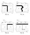
- FIG. 6illustrates a 180 degree phase shifter in the prior art
- FIG. 7illustrates a block diagram of a 180 degree phase shifter, in one embodiment in accordance with the present invention.
- FIG. 8illustrates a 180 degree phase shifter including delay elements, in one alternative embodiment in accordance with the present invention.
- FIG. 9illustrates a 180 degree phase shifter including a single delay element, in one alternative embodiment in accordance with the present invention.
- FIG. 10illustrates a flow diagram showing an exemplary process for selectively phase shifting an RF signal according to one embodiment in accordance with the present invention.
- a system for a wireless (i.e., radio frequency or RF) link to a remote receiving deviceincludes a circuit board comprising communication circuitry for generating an RF signal and an antenna apparatus for transmitting and/or receiving the RF signal.
- the antenna apparatusincludes two or more antenna elements arranged near the periphery of the circuit board. Each of the antenna elements provides a directional radiation pattern.
- the antenna elementsmay be electrically selected (e.g., switched on or off) so that the antenna apparatus may form configurable radiation patterns. If multiple antenna elements are switched on, the antenna apparatus may form an omnidirectional radiation pattern.
- the circuit boardinterconnects the communication circuitry and provides the antenna apparatus in one easily manufacturable printed circuit board. Including the antenna apparatus in the printed circuit board reduces the cost to manufacture the unit and simplifies interconnection with the communication circuitry. Further, including the antenna apparatus in the circuit board provides more consistent RF matching between the communication circuitry and the antenna elements. A further advantage is that the antenna apparatus radiates directional radiation patterns substantially in the plane of the antenna elements. When mounted horizontally, the radiation patterns are horizontally polarized, so that RF signal transmission indoors is enhanced as compared to a vertically polarized antenna.
- FIG. 1illustrates an exemplary schematic for a system 100 incorporating a circuit board having a peripheral antenna apparatus with selectable elements, in one embodiment in accordance with the present invention.
- the system 100may comprise, for example without limitation, a transmitter/receiver such as an 802.11 access point, an 802.11 receiver, a set-top box, a laptop computer, a television, a cellular telephone, a cordless telephone, a wireless VoIP phone, a remote control, and a remote terminal such as a handheld gaming device.
- the system 100comprises an access point for communicating to one or more remote receiving nodes over a wireless link, for example in an 802.11 wireless network.
- the system 100comprises a circuit board 105 including a radio modulator/demodulator (modem) 120 and a peripheral antenna apparatus 110 .
- the modem 120may include a digital to analog converter (D/A), an oscillator (OSC), mixers (X), and other signal processing circuitry (reverse- ⁇ ).
- the radio modem 120may receive data from a router connected to the Internet (not shown), convert the data into a modulated RF signal, and the antenna apparatus 110 may transmit the modulated RF signal wirelessly to one or more remote receiving nodes (not shown).
- the system 100may also form a part of a wireless local area network by enabling communications among several remote receiving nodes.
- system 100including the circuit board 105
- aspects of the inventionare applicable to a wide variety of appliances, and are not intended to be limited to the disclosed embodiment.
- system 100may be described as transmitting to a remote receiving node via the antenna apparatus 110
- system 100may also receive RF-modulated data from the remote receiving node via the antenna apparatus 110 .
- FIG. 2illustrates the circuit board 105 having the peripheral antenna apparatus 110 of FIG. 1 with selectable elements of FIG. 1 , in one embodiment in accordance with the present invention.
- the circuit board 105comprises a printed circuit board (PCB) such as FR4 material, Rogers 4003 material, or other dielectric material with four layers, although any number of layers is comprehended, such as one or six.
- PCBprinted circuit board
- the circuit board 105includes an area 210 for interconnecting circuitry including for example a power supply 215 , an antenna selector 220 , a data processor 225 , and a radio modulator/demodulator (modem) 230 .
- the data processor 225comprises well-known circuitry for receiving data packets from a router connected to the Internet (e.g., via a local area network).
- the radio modem 230comprises communication circuitry including virtually any device for converting the data packets processed by the data processor 225 into a modulated RF signal for transmission to one or more of the remote receiving nodes, and for reception therefrom.
- the radio modem 230comprises circuitry for converting the data packets into an 802.11 compliant modulated RF signal.
- the circuit board 105also includes a microstrip RF line 234 for routing the modulated RF signal to an antenna feed port 235 .
- an antenna feed port 235is configured to distribute the modulated RF signal directly to antenna elements 240 A, 240 B, 240 C, 240 D, 240 E, 240 F, 240 G of the peripheral antenna apparatus 110 (not labeled) by way of antenna feed lines.
- antenna elements 240 A, 240 B, 240 C, 240 D, 240 E, 240 F, 240 G of the peripheral antenna apparatus 110not labeled
- the antenna feed port 235is configured to distribute the modulated RF signal to one or more of the selectable antenna elements 240 A- 240 G by way of a switching network 237 and microstrip feed lines 239 A, 239 B, 239 C, 239 D, 239 E, 239 F, 239 G.
- the feed lines 239 A- 239 Gmay also comprise coupled microstrip, coplanar strips with impedance transformers, coplanar waveguide, coupled strips, and the like.
- the antenna feed port 235 , the switching network 237 , and the feed lines 239 A- 239 Gcomprise switching and routing components on the circuit board 105 for routing the modulated RF signal to the antenna elements 240 A- 240 G.
- the antenna feed port 235 , the switching network 237 , and the feed lines 239 A- 239 Ginclude structures for impedance matching between the radio modem 230 and the antenna elements 240 A- 240 G.
- the antenna feed port 235 , the switching network 237 , and the feed lines 239 A- 239 Gare further described with respect to FIG. 5 .
- the peripheral antenna apparatuscomprises a plurality of antenna elements 240 A- 240 G located near peripheral areas of the circuit board 105 .
- Each of the antenna elements 240 A- 240 Gproduces a directional radiation pattern with gain (as compared to an omnidirectional antenna) and with polarization substantially in the plane of the circuit board 105 .
- Each of the antenna elementsmay be arranged in an offset direction from the other antenna elements 240 A- 240 G so that the directional radiation pattern produced by one antenna element (e.g., the antenna element 240 A) is offset in direction from the directional radiation pattern produced by another antenna element (e.g., the antenna element 240 C).
- Certain antenna elementsmay also be arranged in substantially the same direction, such as the antenna elements 240 D and 240 E. Arranging two or more of the antenna elements 240 A- 240 G in the same direction provides spatial diversity between the antenna elements 240 A- 240 G so arranged.
- selecting various combinations of the antenna elements 240 A- 240 Gproduces various radiation patterns ranging from highly directional to omnidirectional.
- enabling adjacent antenna elements 240 A- 240 Gresults in higher directionality in azimuth as compared to selecting either of the antenna elements 240 A- 240 G alone.
- selecting the adjacent antenna elements 240 A and 240 Bmay provide higher directionality than selecting either of the antenna elements 240 A or 240 B alone.
- selecting every other antenna elemente.g., the antenna elements 240 A, 240 C, 240 E, and 240 G
- all of the antenna elements 240 A- 240 Gmay produce an omnidirectional radiation pattern.
- FIG. 3Aillustrates the antenna element 240 A of FIG. 2 , in one embodiment in accordance with the present invention.
- the antenna element 240 A of this embodimentcomprises a modified dipole with components on both exterior surfaces of the circuit board 105 (considered as the plane of FIG. 3A ).
- the antenna element 240 Aincludes a first dipole component 310 .
- the antenna element 240 Aincludes a second dipole component 311 extending substantially opposite from the first dipole component 310 .
- the first dipole component 310 and the second dipole component 311form the antenna element 240 A to produce a generally cardioid directional radiation pattern substantially in the plane of the circuit board.
- the dipole component 310 and/or the dipole component 311may be bent to conform to an edge of the circuit board 105 . Incorporating the bend in the dipole component 310 and/or the dipole component 311 may reduce the size of the circuit board 105 .
- the dipole components 310 and 311are formed on interior layers of the circuit board, as described herein.
- the antenna element 240 Amay optionally include one or more reflectors (e.g., the reflector 312 ).
- the reflector 312comprises elements that may be configured to concentrate the directional radiation pattern formed by the first dipole component 310 and the second dipole component 311 .
- the reflector 312may also be configured to broaden the frequency response of the antenna component 240 A. In some embodiments, the reflector 312 broadens the frequency response of each modified dipole to about 300 MHz to 500 MHz.
- the combined operational bandwidth of the antenna apparatus resulting from coupling more than one of the antenna elements 240 A- 240 G to the antenna feed port 235is less than the bandwidth resulting from coupling only one of the antenna elements 240 A- 240 G to the antenna feed port 235 .
- the combined frequency response of the antenna apparatusis about 90 MHz.
- coupling more than one of the antenna elements 240 A- 240 G to the antenna feed port 235maintains a match with less than 10 dB return loss over 802.11 wireless LAN frequencies, regardless of the number of antenna elements 240 A- 240 G that are switched on.
- FIG. 3Billustrates the antenna element 240 A of FIG. 2 , in an alternative embodiment in accordance with the present invention.
- the antenna element 240 A of this embodimentmay be reduced in dimension as compared to the antenna element 240 A of FIG. 3A .
- the antenna element 240 A of this embodimentcomprises a first dipole component 315 incorporating a meander line shape, a second dipole component 316 incorporating a corresponding meander line shape, and a reflector 317 . Because of the meander line shape, the antenna element 240 A of this embodiment may require less space on the circuit board 105 as compared to the antenna element 240 A of FIG. 3A .
- FIG. 3Cillustrates the antenna element 240 A of FIG. 2 , in an alternative embodiment in accordance with the present invention.
- the antenna element 240 A of this embodimentincludes one or more components on one or more layers internal to the circuit board 105 .
- a first dipole component 321is formed on an internal ground plane of the circuit board 105 .
- a second dipole component 322is formed on an exterior surface of the circuit board 105 .
- a reflector 323may be formed internal to the circuit board 105 , or may be formed on the exterior surface of the circuit board 105 .
- An advantage of this embodiment of the antenna element 240 Ais that vias through the circuit board 105 may be reduced or eliminated, making the antenna element 240 A of this embodiment less expensive to manufacture.
- FIG. 3Dillustrates the antenna element 240 A of FIG. 2 , in an alternative embodiment in accordance with the present invention.
- the antenna element 240 A of this embodimentincludes a modified dipole with a microstrip to coplanar strip (CPS) transition 332 and CPS dipole arms 330 A and 330 B on a surface layer of the circuit board 105 .
- CPSmicrostrip to coplanar strip
- this embodimentprovides that the CPS dipole arm 330 A may be coplanar with the CPS dipole arm 330 B, and may be formed on the same surface of the circuit board 105 .
- This embodimentmay also include a reflector 331 formed on one or more interior layers of the circuit board 105 or on the opposite surface of the circuit board 105 .
- An advantage of this embodimentis that no vias are needed in the circuit board 105 .
- the dimensions of the individual components of the antenna elements 240 A- 240 Gdepend upon a desired operating frequency of the antenna apparatus.
- the dimensions of wavelengthdepend upon conductive and dielectric materials comprising the circuit board 105 , because speed of electron propagation depends upon the properties of the circuit board 105 material. Therefore, dimensions of wavelength referred to herein are intended specifically to incorporate properties of the circuit board, including considerations such as the conductive and dielectric properties of the circuit board 105 .
- the dimensions of the individual componentsmay be established by use of RF simulation software, such as IE3D from Zeland Software of Fremont, Calif.
- FIG. 4illustrates the antenna element 240 A of FIG. 3A , showing multiple layers of the circuit board 105 , in one embodiment of the invention.
- the circuit board 105 of this embodimentcomprises a 60 mil thick stackup with three dielectrics and four metallization layers A-D, with an internal RF ground plane at layer B (10 mils from top layer A to the internal ground layer B).
- Layer Bis separated by a 40 mil thick dielectric to the next layer C, which may comprise a power plane.
- Layer Cis separated by a 10 mil dielectric to the bottom layer D.
- the first dipole component 310 and portions 412 A of the reflector 312is formed on the first (exterior) surface layer A.
- the second metallization layer Bwhich includes a connection to the ground layer (depicted as an open trace)
- corresponding portions 412 B of the reflector 312are formed.
- the third metallization layer Ccorresponding portions 412 C of the reflector 312 are formed.
- the second dipole component 411 Dis formed along with corresponding portions of the reflector 412 D on the fourth (exterior) surface metallization layer D.
- the reflectors 412 A- 412 D and the second dipole component 411 B- 411 D on the different layersare interconnected to the ground layer B by an array of metalized vias 415 (only one via 415 shown, for clarity) spaced less than 1/20th of a wavelength apart, as determined by an operating RF frequency range of 2.4-2.5 GHz for an 802.11 configuration. It will be apparent to a person or ordinary skill that the reflector 312 comprises four layers, depicted as 412 A- 412 D.
- An advantage of the antenna element 240 A of FIG. 4is that transitions in the RF path are avoided. Further, because of the cutaway portion of the reflector 412 A and the array of vias interconnecting the layers of the circuit board 105 , the antenna element 240 A of this embodiment offers a good ground plane for the ground dipole 311 and the reflector element 312 .
- FIG. 5Aillustrates the antenna feed port 235 and the switching network 237 of FIG. 2 , in one embodiment in accordance with the present invention.
- the antenna feed port 235 of this embodimentreceives the RF line 234 from the radio modem 230 into a distribution point 235 A. From the distribution point 235 A, impedance matched RF traces 515 A, 515 B, 515 C, 515 D, 515 E, 515 F, 515 G extend to PIN diodes 520 A, 520 B, 520 C, 520 D, 520 E, 520 F, 520 G.
- the RF traces 515 A- 515 Gcomprise 20 mils wide traces, based upon a 10 mil dielectric from the internal ground layer (e.g., the ground layer B of FIG. 4 ).
- Feed lines 239 A- 239 Gextend from the PIN diodes 520 A- 520 G to each of the antenna elements 240 A- 240 G.
- Each PIN diodecomprises a single-pole single-throw switch to switch each antenna element either on or off (i.e., couple or decouple each of the antenna elements 240 A- 240 G to the antenna feed port 235 ).
- a series of control signals(not shown) is used to bias each PIN diode. With the PIN diode forward biased and conducting a DC current, the PIN diode is switched on, and the corresponding antenna element is selected. With the PIN diode reverse biased, the PIN diode is switched off.
- the RF traces 515 A- 515 Gare of length equal to a multiple of one half wavelength from the antenna feed port 235 .
- the RF traces 515 A- 515 Gmay be unequal in length, but multiples of one half wavelength from the antenna feed port 235 .
- the RF trace 515 Amay be of zero length so that the PIN diode 520 A is directly attached to the antenna feed port 235 .
- the RF trace 515 Bmay be one half wavelength
- the RF trace 515 Cmay be one wavelength, and so on, in any combination.
- the PIN diodes 520 A- 520 Gare multiples of one half wavelength from the antenna feed port 235 so that disabling one PIN diode (e.g. the PIN diode 520 A) does not create an RF mismatch that would cause RF reflections back to the distribution point 235 A and to other traces that are enabled (e.g., the trace 515 B).
- the PIN diode 540 Ais “off,” the radio modem 230 sees a high impedance on the trace 515 A, and the impedance of the trace 515 B that is “on” is virtually unaffected by the PIN diode 520 A.
- the PIN diodes 520 A- 520 Gare located at an offset from the one half wavelength distance. The offset is determined to account for stray capacitance in the distribution point 235 A and/or the PIN diodes 520 A- 520 G.
- FIG. 5Billustrates the antenna feed port 235 and the switching network 237 of FIG. 2 , in an alternative embodiment in accordance with the present invention.
- the antenna feed port 235 of this embodimentreceives the RF line 234 from the radio modem 230 into a distribution point 235 B.
- the distribution point 235 B of this embodimentis configured as a solder pad for the PIN diodes 520 A- 520 G.
- the PIN diodes 520 A- 520 Gare soldered between the distribution point 235 B and the ends of the feed lines 239 A- 239 G.
- the distribution point 235 B of this embodimentacts as a zero wavelength distance from the antenna feed port 235 .
- An advantage of this embodimentis that the feed lines extending from the PIN diodes 520 A- 520 G to the antenna elements 240 A- 240 G offer unbroken controlled impedance.
- FIG. 5Cillustrates the antenna feed port and the switching network of FIG. 2 , in an alternative embodiment in accordance with the present invention.
- This embodimentmay be considered as a combination of the embodiments depicted in FIGS. 5A and 5B .
- the PIN diodes 520 A, 520 C, 520 E, and 520 Gare connected to the RF traces 515 A, 515 C, 515 E, and 515 G, respectively, in similar fashion to that described with respect to FIG. 5A .
- the PIN diodes 520 B, 520 D, and 520 Fare soldered to a distribution point 235 C and to the corresponding feed lines 239 B, 239 D, and 239 F, in similar fashion to that described with respect to FIG. 5B .
- the switching network 237is described as comprising PIN diodes 520 , it will be appreciated that the switching network 237 may comprise virtually any RF switching device such as a GaAs FET, as is well known in the art.
- the switching network 237comprises one or more single-pole multiple-throw switches.
- one or more light emitting diodesare coupled to the switching network 237 or the feed lines 239 A- 239 G as a visual indicator of which of the antenna elements 240 A- 240 G is on or off.
- a light emitting diodeis placed in circuit with each PIN diode 520 so that the light emitting diode is lit when the corresponding antenna element is selected.
- the lengths of the antenna feed lines 239 A- 239 Gmay not comprise equivalent lengths from the antenna feed port 235 .
- Unequal lengths of the antenna feed lines 239 A- 239 Gmay result in phase offsets between the antenna elements 240 A- 240 G. Accordingly, in some embodiments not shown in FIG.
- each of the feed lines 239 A- 239 G to the antenna elements 240 A- 240 Gare designed to be as long as the longest of the feed lines 239 A- 239 G, even for antenna elements 240 A- 240 G that are relatively close to the antenna feed port 235 .
- the lengths of the feed lines 239 A- 239 Gare designed to be a multiple of a half-wavelength offset from the longest of the feed lines 239 A- 239 G.
- the lengths of the feed lines 239 A- 239 G that are odd multiples of one half wavelength from the other feed lines 239 A- 239 Gincorporate a “phase-inverted” antenna element to compensate for having lengths that are odd multiples of one half wavelength from the other feed lines 239 A- 239 G.
- the antenna elements 240 C and 240 Fare inverted by 180 degrees because the feed lines 239 C and 239 F are 180 degrees out of phase from the feed lines 239 A, 239 B, 239 D, 239 E, and 239 G.
- the first dipole componente.g., surface layer
- the second dipole componente.g., ground layer
- An advantage of the system 100 ( FIG. 1 ) incorporating the circuit board 105 having the peripheral antenna apparatus with selectable antenna elements 240 A- 240 G ( FIG. 2 )is that the antenna elements 240 A- 240 G are constructed directly on the circuit board 105 , therefore the entire circuit board 105 can be easily manufactured at low cost.
- one embodiment or layout of the circuit board 105comprises a substantially square or rectangular shape, so that the circuit board 105 is easily panelized from readily available circuit board material.
- the circuit board 105minimizes or eliminates the possibility of damage to the antenna elements 240 A- 240 G.
- a further advantage of the circuit board 105 incorporating the peripheral antenna apparatus with selectable antenna elements 240 A- 240 Gis that the antenna elements 240 A- 240 G may be configured to reduce interference in the wireless link between the system 100 and a remote receiving node.
- the system 100 communicating over the wireless link to the remote receiving nodemay select a particular configuration of selected antenna elements 240 A- 240 G that minimizes interference over the wireless link. For example, if an interfering signal is received strongly via the antenna element 240 C, and the remote receiving node is received strongly via the antenna element 240 A, selecting only the antenna element 240 A may reduce the interfering signal as opposed to selecting the antenna element 240 C.
- the system 100may select a configuration of selected antenna elements 240 A- 240 G corresponding to a maximum gain between the system and the remote receiving node. Alternatively, the system 100 may select a configuration of selected antenna elements 240 A- 240 G corresponding to less than maximal gain, but corresponding to reduced interference. Alternatively, the antenna elements 240 A- 240 G may be selected to form a combined omnidirectional radiation pattern.
- the directional radiation pattern of the antenna elements 240 A- 240 Gis substantially in the plane of the circuit board 105 .
- the corresponding radiation patterns of the antenna elements 240 A- 240 Gare horizontally polarized.
- Horizontally polarized RF energytends to propagate better indoors than vertically polarized RF energy.
- Providing horizontally polarized signalsimproves interference rejection (potentially, up to 20 dB) from RF sources that use commonly-available vertically polarized antennas.
- selectable phase switchingcan be included on the circuit board 105 to provide a number of advantages. For example, incorporating selectable phase switching into the circuit board 105 may allow a reduction in the number of antenna elements 240 A- 240 G used on the circuit board 105 while still providing highly configurable radiation patterns. By selecting two or more of the antenna elements 240 A- 240 G and by shifting one or more of the antenna elements 240 A- 240 G by 180 degrees, for example, the resulting radiation pattern may overlap a radiation pattern of another of the antenna elements 240 A- 240 G, rendering some of the antenna elements 240 A- 240 G redundant, or rendering unnecessary the addition of some antenna elements at particular orientations.
- incorporating selectable phase shifting into the circuit board 105may allow a reduction in the number of antenna elements 240 A- 240 G and a reduction in the overall size of the circuit board 105 . Because the cost of the circuit board 105 is dependent upon the amount of area of the PCB included in the circuit board 105 , selectable phase shifting allows cost reduction in that fewer antenna elements 240 A- 240 G may be used for a given number of radiation patterns.
- selectable phase shiftingin the context of configurable antenna elements 240 A- 240 G as described with respect to the circuit board 105 .
- selectable phase shiftinghas broad applicablity in RF coupling networks and is not limited merely to embodiments for antenna coupling.
- selectable phase shifting as described further hereinhas applicability to signal cancellation such as is generally used in band-stop or notch filters.
- FIG. 6illustrates a 180 degree phase shifter 600 in the prior art.
- two PIN diodes 610allow RF to travel through a straight-through path from an input port to an output port.
- two PIN diodes 620allow RF to travel through a 180 degree phase shift ( ⁇ /2 or 1 ⁇ 2-wavelength) path from the input port to the output port.
- FIG. 7illustrates a block diagram of a 180 degree phase shifter 700 , in one embodiment in accordance with the present invention.
- the phase shifter 700may be included in the various embodiments of the switching network 237 depicted in FIGS. 5A , 5 B, and 5 C, for example, to implement selectable phase shifting for one or more of the antenna elements 240 A- 240 G of FIG. 2 .
- the phase shifter 700includes a first PIN diode 710 along a straight-though path between the input port and the output port, a first PCB trace line 705 of 1 ⁇ 4-wavelength (i.e,. ⁇ /4) of phase delay, a second PCB trace line 706 of 1 ⁇ 4-wavelength (i.e., ⁇ /4) of phase delay, and a second PIN diode 715 at the confluence of the first trace line 705 and the second trace line 706 .
- the phase shifter 700takes advantage of the property of 1 ⁇ 4-wavelength transmission lines that a short to ground, a quarter-wavelength away from the opposite end of the 1 ⁇ 4-wavelength transmission line, is an open.
- the trace lines 705 and 706appear as high impedance at the input port and the output port.
- the inputis directly connected to the output through the PIN diode 710 .
- the 1 ⁇ 4-wavelength trace lines 705 and 706present a negligible impact on the RF at the input or output ports because a short to ground at the second PIN diode 715 , a quarter-wavelength away at the input and output ports, is an open.
- an RF signal at the input portis directed through the two 1 ⁇ 4-wavelength trace lines 705 and 706 and is thereby shifted in phase by 180 degrees at the output port.
- phase shifter 600that requires four PIN diodes, therefore, selecting between a straight-through path or a 180 degree phase shifted path requires only two PIN diodes 710 and 715 .
- one or more RF switchesmay replace the PIN diodes.
- the input port“sees” high impedance to the output port due to the first PIN diode 710 and also sees high impedance due to the 1 ⁇ 4-wavelength trace lines 705 and 706 . Therefore, the output port is isolated from the input port.
- the antenna elementwould be off with the first PIN diode 710 biased off and the second PIN diode 715 biased on.
- a special caseoccurs with the first PIN diode 710 biased on and the second PIN diode 715 biased off.
- RF at the input portsees a low impedance coupling to the output port through the first PIN diode 710 .
- the RFalso transmits through the 1 ⁇ 4-wavelength trace lines 705 and 706 .
- the in-phase RF through the straight-through pathis coupled to 180 degree phase shifted RF, and essentially the phase shifter 700 performs as a band-stop filter or a notch filter tuned to the wavelength (inverse of frequency) of the 1 ⁇ 4-wavelength trace lines 705 and 706 .
- the first PCB trace lineis a multiple of 1 ⁇ 4 wavelength of phase delay and the second PCB trace line is also a multiple of 1 ⁇ 4 wavelength of phase delay.
- the first PCB trace lineis 3 ⁇ 4 wavelength of phase delay and the second PCB trace line is also 3 ⁇ 4 wavelength of phase delay.
- the first PCB trace lineis 1 ⁇ 2 wavelength of phase delay and the second PCB trace line is also 1 ⁇ 2 wavelength of phase delay.
- an RF signalis shifted in phase by 360 degrees at the output port.
- FIG. 8illustrates a 180 degree phase shifter 800 including delay elements, in one alternative embodiment in accordance with the present invention.
- the phase shifter 800includes a first PIN diode 810 along a straight-though path between the input port and the output port, and a second PIN diode 815 at the confluence of 1 ⁇ 4-wavelength delay paths.
- delay elements 825 and 826are provided so that the trace lines 805 and 806 may be made physically shorter than the corresponding trace lines 705 and 706 .
- the delay elements 825 and 826comprise delay lines in one embodiment.
- the delay elements 825 and 826comprise all-pass filters, similar in function to delay lines, to provide a predetermined phase shift or group delay.
- Persons of ordinary skillwill recognize that there are many possible embodiments for the delay elements 825 and 826 .
- the delay elements 825 and 826comprise well-known resistors, capacitors (fixed or voltage controlled), inductors, and the like, configured to provide a predetermined phase shift or group delay.
- a first PCB trace line 805is of length 1 ⁇ 4-wavelength (i.e., ⁇ /4) of phase delay less the amount of delay presented by the delay element 825 ( ⁇ /4-delay).
- a second PCB trace line 806is of length 1 ⁇ 4-wavelength (i.e., ⁇ /4) of phase delay less the amount of delay presented by the delay element 826 ( ⁇ /4-delay).
- the phase shifter 800can provide a straight-through path between the input port and the output port, a 180 degree phase shift, a high impedance between the input port and the output port, or a notch or band-stop filter.
- FIG. 9illustrates a 180 degree phase shifter 900 including a single delay element, in one alternative embodiment in accordance with the present invention.
- the phase shifter 900includes a first PIN diode 910 along a straight-though path between the input port and the output port.
- a single delay element 925is provided so that trace lines 905 and 906 may be made physically shorter than the corresponding trace lines 705 and 706 of FIG. 7 .
- the delay element 925comprises a delay line, an all-pass filter, or the like to provide a predetermined phase shift or group delay.
- a second PIN diode 915completes the phase shifter 900 by selectively coupling the delay element 925 to ground.
- a first PCB trace line 905is of length 1 ⁇ 4-wavelength (i.e., ⁇ /4) of phase delay less the amount of delay presented by the delay element 925 ( ⁇ /4-delay).
- a second PCB trace line 906is of length 1 ⁇ 4-wavelength (i.e., ⁇ /4) of phase delay less the amount of delay presented by the delay element 825 ( ⁇ /4-delay).
- FIG. 10illustrates a flow diagram showing an exemplary process for selectively phase shifting an RF signal according to one embodiment in accordance with the present invention.
- the processmay begin with “START” and end with “END.”
- an RF signalis received at an input port.
- a straight-through path between the input port and an output portis selectively disabled by zero- or reverse-biasing a first PIN diode included in the straight-through path.
- the straight-through pathmay include the first PIN diode 710 discussed with respect to the embodiment of FIG. 7 such that enabling the first PIN diode 710 couples the input port to the output port through the straight-through path. Disabling the first PIN diode 710 decouples or isolates the input port and the output port.
- the RF signalis phase shifted by enabling a “long path” of a predetermined length (or delay, as length is related to delay for RF) coupled to the input port by opening (applying a zero or reverse bias to) a second PIN diode included in the long path, the second PIN diode coupled to ground.
- the long pathmay comprise the PCB trace lines 705 and 706 of 1 ⁇ 4-wavelength, and a second PIN diode 715 at the confluence of the first trace line 705 and the second trace line 706 of FIG. 7 , for example.
- the long pathmay optionally include one or more delay elements, as described with respect to FIGS. 8 and 9 .
- the predetermined length of the long pathis ⁇ /2, according to exemplary embodiments.
- the phase shifted RF signalis transmitted through an output port coupled to the straight-through path and the long path.
- Selectable phase switching as described hereinprovides a number of advantages and is widely applicable to RF networks, just a few of which are described herein. Incorporating selectable phase switching into the circuit board 105 may allow a reduction in the number of antenna elements 240 A- 240 G used on the circuit board 105 while still providing highly configurable radiation patterns. Further, as compared to a prior art phase shifter, selectable phase shifting as described herein reduces the number of PIN diodes used in selecting non-phase shifted or phase shifted RF paths.
Landscapes
- Variable-Direction Aerials And Aerial Arrays (AREA)
Abstract
Description
Claims (33)
Priority Applications (2)
| Application Number | Priority Date | Filing Date | Title |
|---|---|---|---|
| US11/265,751US7498999B2 (en) | 2004-11-22 | 2005-11-01 | Circuit board having a peripheral antenna apparatus with selectable antenna elements and selectable phase shifting |
| TW094141018ATWI426653B (en) | 2004-11-22 | 2005-11-22 | Circuit board having a peripheral antenna apparatus with selectable antenna elements and selectable phase shifting |
Applications Claiming Priority (3)
| Application Number | Priority Date | Filing Date | Title |
|---|---|---|---|
| US63049904P | 2004-11-22 | 2004-11-22 | |
| US11/022,080US7193562B2 (en) | 2004-11-22 | 2004-12-23 | Circuit board having a peripheral antenna apparatus with selectable antenna elements |
| US11/265,751US7498999B2 (en) | 2004-11-22 | 2005-11-01 | Circuit board having a peripheral antenna apparatus with selectable antenna elements and selectable phase shifting |
Related Parent Applications (1)
| Application Number | Title | Priority Date | Filing Date |
|---|---|---|---|
| US11/022,080Continuation-In-PartUS7193562B2 (en) | 2004-08-18 | 2004-12-23 | Circuit board having a peripheral antenna apparatus with selectable antenna elements |
Publications (2)
| Publication Number | Publication Date |
|---|---|
| US20060109067A1 US20060109067A1 (en) | 2006-05-25 |
| US7498999B2true US7498999B2 (en) | 2009-03-03 |
Family
ID=36460401
Family Applications (1)
| Application Number | Title | Priority Date | Filing Date |
|---|---|---|---|
| US11/265,751Expired - Fee RelatedUS7498999B2 (en) | 2004-11-22 | 2005-11-01 | Circuit board having a peripheral antenna apparatus with selectable antenna elements and selectable phase shifting |
Country Status (2)
| Country | Link |
|---|---|
| US (1) | US7498999B2 (en) |
| CN (1) | CN1934750B (en) |
Cited By (24)
| Publication number | Priority date | Publication date | Assignee | Title |
|---|---|---|---|---|
| US20070156885A1 (en)* | 2003-03-03 | 2007-07-05 | Hooker Guy A | Management interface for radio stations |
| US20080136715A1 (en)* | 2004-08-18 | 2008-06-12 | Victor Shtrom | Antenna with Selectable Elements for Use in Wireless Communications |
| US20080151745A1 (en)* | 2006-12-20 | 2008-06-26 | General Instrument Corporation | Active link cable mesh |
| US20080268778A1 (en)* | 2005-03-09 | 2008-10-30 | De La Garrigue Michael | Media Access Controller for Use in a Multi-Sector Access Point Array |
| US20090059875A1 (en)* | 2007-06-18 | 2009-03-05 | Xirrus, Inc. | Node fault identification in wireless lan access points |
| US20100119002A1 (en)* | 2008-11-12 | 2010-05-13 | Xirrus, Inc. | Mimo antenna system |
| US20110228870A1 (en)* | 2006-02-28 | 2011-09-22 | Rotani, Inc. | Method and Apparatus for Overlapping MIMO Physical Sectors |
| US20120212304A1 (en)* | 2011-02-18 | 2012-08-23 | Cemin Zhang | Absorptive tunable bandstop filter with wide tuning range and electrically tunable all-pass filter useful therein |
| US8422540B1 (en) | 2012-06-21 | 2013-04-16 | CBF Networks, Inc. | Intelligent backhaul radio with zero division duplexing |
| US8467363B2 (en) | 2011-08-17 | 2013-06-18 | CBF Networks, Inc. | Intelligent backhaul radio and antenna system |
| US20130207740A1 (en)* | 2012-02-14 | 2013-08-15 | Murata Manufacturing Co., Ltd. | High-frequency signal transmission line and electronic apparatus including the same |
| US8581794B1 (en) | 2010-03-04 | 2013-11-12 | Qualcomm Incorporated | Circular antenna array systems |
| US8686905B2 (en) | 2007-01-08 | 2014-04-01 | Ruckus Wireless, Inc. | Pattern shaping of RF emission patterns |
| US8704720B2 (en) | 2005-06-24 | 2014-04-22 | Ruckus Wireless, Inc. | Coverage antenna apparatus with selectable horizontal and vertical polarization elements |
| US8723741B2 (en) | 2009-03-13 | 2014-05-13 | Ruckus Wireless, Inc. | Adjustment of radiation patterns utilizing a position sensor |
| US8756668B2 (en) | 2012-02-09 | 2014-06-17 | Ruckus Wireless, Inc. | Dynamic PSK for hotspots |
| US8830854B2 (en) | 2011-07-28 | 2014-09-09 | Xirrus, Inc. | System and method for managing parallel processing of network packets in a wireless access device |
| US8868002B2 (en) | 2011-08-31 | 2014-10-21 | Xirrus, Inc. | System and method for conducting wireless site surveys |
| US9055450B2 (en) | 2011-09-23 | 2015-06-09 | Xirrus, Inc. | System and method for determining the location of a station in a wireless environment |
| US9092610B2 (en) | 2012-04-04 | 2015-07-28 | Ruckus Wireless, Inc. | Key assignment for a brand |
| US20160013563A1 (en)* | 2013-07-12 | 2016-01-14 | CommScope Technologies, LLC | Wideband Twin Beam Antenna Array |
| US9379456B2 (en) | 2004-11-22 | 2016-06-28 | Ruckus Wireless, Inc. | Antenna array |
| US9634403B2 (en) | 2012-02-14 | 2017-04-25 | Ruckus Wireless, Inc. | Radio frequency emission pattern shaping |
| US10186750B2 (en) | 2012-02-14 | 2019-01-22 | Arris Enterprises Llc | Radio frequency antenna array with spacing element |
Families Citing this family (38)
| Publication number | Priority date | Publication date | Assignee | Title |
|---|---|---|---|---|
| US20080219246A1 (en)* | 2007-03-08 | 2008-09-11 | Northrop Grumman Space And Mission Systems Corp. | System and method for switching using coordinated phase shifters |
| US8014373B2 (en)* | 2007-09-19 | 2011-09-06 | John Mezzalingua Associates, Inc. | Filtered antenna assembly |
| US8416031B2 (en)* | 2007-12-21 | 2013-04-09 | Hollinworth Fund, L.L.C. | Multiple pole multiple throw switch device based on composite right and left handed metamaterial structures |
| US7978139B2 (en)* | 2009-06-18 | 2011-07-12 | Bae Systems Information And Electronic Systems Integration Inc. | Direction finding and geolocation of wireless devices |
| US7978138B2 (en)* | 2009-06-18 | 2011-07-12 | Bae Systems Information And Electronic Systems Integration Inc. | Direction finding of wireless devices |
| US8089406B2 (en)* | 2009-06-18 | 2012-01-03 | Bae Systems Information And Electronic Systems Integration Inc. | Locationing of communication devices |
| US7986271B2 (en)* | 2009-06-18 | 2011-07-26 | Bae Systems Information And Electronic Systems Integration Inc. | Tracking of emergency personnel |
| US8373596B1 (en) | 2010-04-19 | 2013-02-12 | Bae Systems Information And Electronic Systems Integration Inc. | Detecting and locating RF emissions using subspace techniques to mitigate interference |
| US8963656B2 (en) | 2010-05-24 | 2015-02-24 | Silicon Image, Inc. | Apparatus, system, and method for a compact symmetrical transition structure for radio frequency applications |
| US9407012B2 (en) | 2010-09-21 | 2016-08-02 | Ruckus Wireless, Inc. | Antenna with dual polarization and mountable antenna elements |
| US8577321B2 (en) | 2010-12-02 | 2013-11-05 | Apple, Inc. | Methods for selecting antennas to avoid signal bus interference |
| US8989672B2 (en) | 2011-01-07 | 2015-03-24 | Apple Inc. | Methods for adjusting radio-frequency circuitry to mitigate interference effects |
| CN103165983A (en) | 2011-12-16 | 2013-06-19 | 华为技术有限公司 | A kind of antenna device, equipment and signal transmitting device |
| WO2013173250A1 (en) | 2012-05-13 | 2013-11-21 | Invention Mine Llc | Full duplex wireless transmission with self-interference cancellation |
| US9997830B2 (en) | 2012-05-13 | 2018-06-12 | Amir Keyvan Khandani | Antenna system and method for full duplex wireless transmission with channel phase-based encryption |
| US9570799B2 (en) | 2012-09-07 | 2017-02-14 | Ruckus Wireless, Inc. | Multiband monopole antenna apparatus with ground plane aperture |
| CN104143683A (en)* | 2013-05-10 | 2014-11-12 | 华为终端有限公司 | Terminal device |
| US10177896B2 (en) | 2013-05-13 | 2019-01-08 | Amir Keyvan Khandani | Methods for training of full-duplex wireless systems |
| TWI572088B (en)* | 2013-09-14 | 2017-02-21 | 瑞昱半導體股份有限公司 | Wireless communication apparatus and controlling method thereof |
| EP3058770A4 (en) | 2013-10-20 | 2017-06-14 | Arbinder Singh Pabla | Wireless system with configurable radio and antenna resources |
| US9236996B2 (en) | 2013-11-30 | 2016-01-12 | Amir Keyvan Khandani | Wireless full-duplex system and method using sideband test signals |
| US9820311B2 (en) | 2014-01-30 | 2017-11-14 | Amir Keyvan Khandani | Adapter and associated method for full-duplex wireless communication |
| US9912079B2 (en)* | 2014-07-03 | 2018-03-06 | Xirrus, Inc. | Distributed omni-dual-band antenna system for a Wi-Fi access point |
| US9686001B1 (en) | 2015-11-27 | 2017-06-20 | Huawei Technologies Co., Ltd. | Beem-steering apparatus for an antenna array |
| US10333593B2 (en) | 2016-05-02 | 2019-06-25 | Amir Keyvan Khandani | Systems and methods of antenna design for full-duplex line of sight transmission |
| WO2018094625A1 (en)* | 2016-11-23 | 2018-05-31 | 深圳市大疆创新科技有限公司 | Frame of unmanned aerial vehicle, unmanned aerial vehicle and antenna switching method |
| US10700766B2 (en) | 2017-04-19 | 2020-06-30 | Amir Keyvan Khandani | Noise cancelling amplify-and-forward (in-band) relay with self-interference cancellation |
| US11191126B2 (en) | 2017-06-05 | 2021-11-30 | Everest Networks, Inc. | Antenna systems for multi-radio communications |
| US10714830B2 (en)* | 2017-10-03 | 2020-07-14 | Hughes Network Systems, Llc | Digital phase shifter switch and transmission line reduction |
| US11057204B2 (en) | 2017-10-04 | 2021-07-06 | Amir Keyvan Khandani | Methods for encrypted data communications |
| US11012144B2 (en) | 2018-01-16 | 2021-05-18 | Amir Keyvan Khandani | System and methods for in-band relaying |
| US10433262B1 (en)* | 2018-03-22 | 2019-10-01 | Panasonic Avionics Corporation | Density optimized bluetooth antenna |
| US10879627B1 (en) | 2018-04-25 | 2020-12-29 | Everest Networks, Inc. | Power recycling and output decoupling selectable RF signal divider and combiner |
| US11050470B1 (en) | 2018-04-25 | 2021-06-29 | Everest Networks, Inc. | Radio using spatial streams expansion with directional antennas |
| US11005194B1 (en) | 2018-04-25 | 2021-05-11 | Everest Networks, Inc. | Radio services providing with multi-radio wireless network devices with multi-segment multi-port antenna system |
| US11089595B1 (en) | 2018-04-26 | 2021-08-10 | Everest Networks, Inc. | Interface matrix arrangement for multi-beam, multi-port antenna |
| CN109004365A (en)* | 2018-06-26 | 2018-12-14 | 浙江大学 | A kind of microwave or millimeter wave amplitude and phase control circuit based on directional coupler |
| KR102597392B1 (en)* | 2019-02-28 | 2023-11-03 | 삼성전자주식회사 | Antenna module supporting dual bands and electronic device including the same |
Citations (164)
| Publication number | Priority date | Publication date | Assignee | Title |
|---|---|---|---|---|
| US723188A (en) | 1900-07-16 | 1903-03-17 | Nikola Tesla | Method of signaling. |
| US1869659A (en) | 1929-10-12 | 1932-08-02 | Broertjes Willem | Method of maintaining secrecy in the transmission of wireless telegraphic messages |
| US2292387A (en) | 1941-06-10 | 1942-08-11 | Markey Hedy Kiesler | Secret communication system |
| US3488445A (en) | 1966-11-14 | 1970-01-06 | Bell Telephone Labor Inc | Orthogonal frequency multiplex data transmission system |
| US3568105A (en)* | 1969-03-03 | 1971-03-02 | Itt | Microstrip phase shifter having switchable path lengths |
| US3967067A (en) | 1941-09-24 | 1976-06-29 | Bell Telephone Laboratories, Incorporated | Secret telephony |
| US3982214A (en)* | 1975-10-23 | 1976-09-21 | Hughes Aircraft Company | 180° phase shifting apparatus |
| US3991273A (en) | 1943-10-04 | 1976-11-09 | Bell Telephone Laboratories, Incorporated | Speech component coded multiplex carrier wave transmission |
| US4001734A (en)* | 1975-10-23 | 1977-01-04 | Hughes Aircraft Company | π-Loop phase bit apparatus |
| US4176356A (en) | 1977-06-27 | 1979-11-27 | Motorola, Inc. | Directional antenna system including pattern control |
| US4193077A (en) | 1977-10-11 | 1980-03-11 | Avnet, Inc. | Directional antenna system with end loaded crossed dipoles |
| US4305052A (en) | 1978-12-22 | 1981-12-08 | Thomson-Csf | Ultra-high-frequency diode phase shifter usable with electronically scanning antenna |
| US4554554A (en) | 1983-09-02 | 1985-11-19 | The United States Of America As Represented By The Secretary Of The Navy | Quadrifilar helix antenna tuning using pin diodes |
| US4733203A (en) | 1984-03-12 | 1988-03-22 | Raytheon Company | Passive phase shifter having switchable filter paths to provide selectable phase shift |
| US4814777A (en) | 1987-07-31 | 1989-03-21 | Raytheon Company | Dual-polarization, omni-directional antenna system |
| WO1990004893A1 (en) | 1988-10-21 | 1990-05-03 | Thomson-Csf | Emitter, transmission method and receiver |
| US5063574A (en) | 1990-03-06 | 1991-11-05 | Moose Paul H | Multi-frequency differentially encoded digital communication for high data rate transmission through unequalized channels |
| US5173711A (en) | 1989-11-27 | 1992-12-22 | Kokusai Denshin Denwa Kabushiki Kaisha | Microstrip antenna for two-frequency separate-feeding type for circularly polarized waves |
| EP0534612A2 (en) | 1991-08-28 | 1993-03-31 | Motorola, Inc. | Cellular system sharing of logical channels |
| US5208564A (en)* | 1991-12-19 | 1993-05-04 | Hughes Aircraft Company | Electronic phase shifting circuit for use in a phased radar antenna array |
| US5220340A (en) | 1992-04-29 | 1993-06-15 | Lotfollah Shafai | Directional switched beam antenna |
| US5282222A (en) | 1992-03-31 | 1994-01-25 | Michel Fattouche | Method and apparatus for multiple access between transceivers in wireless communications using OFDM spread spectrum |
| US5291289A (en) | 1990-11-16 | 1994-03-01 | North American Philips Corporation | Method and apparatus for transmission and reception of a digital television signal using multicarrier modulation |
| US5559800A (en) | 1994-01-19 | 1996-09-24 | Research In Motion Limited | Remote control of gateway functions in a wireless data communication network |
| US5754145A (en) | 1995-08-23 | 1998-05-19 | U.S. Philips Corporation | Printed antenna |
| US5767809A (en) | 1996-03-07 | 1998-06-16 | Industrial Technology Research Institute | OMNI-directional horizontally polarized Alford loop strip antenna |
| US5786793A (en) | 1996-03-13 | 1998-07-28 | Matsushita Electric Works, Ltd. | Compact antenna for circular polarization |
| US5802312A (en) | 1994-09-27 | 1998-09-01 | Research In Motion Limited | System for transmitting data files between computers in a wireless environment utilizing a file transfer agent executing on host system |
| US5964830A (en) | 1995-08-22 | 1999-10-12 | Durrett; Charles M. | User portal device for the world wide web to communicate with a website server |
| US5990838A (en) | 1996-06-12 | 1999-11-23 | 3Com Corporation | Dual orthogonal monopole antenna system |
| US6034638A (en) | 1993-05-27 | 2000-03-07 | Griffith University | Antennas for use in portable communications devices |
| US6091364A (en) | 1996-06-28 | 2000-07-18 | Kabushiki Kaisha Toshiba | Antenna capable of tilting beams in a desired direction by a single feeder circuit, connection device therefor, coupler, and substrate laminating method |
| US6094177A (en) | 1997-11-27 | 2000-07-25 | Yamamoto; Kiyoshi | Planar radiation antenna elements and omni directional antenna using such antenna elements |
| US6169523B1 (en) | 1999-01-13 | 2001-01-02 | George Ploussios | Electronically tuned helix radiator choke |
| JP2001057560A (en) | 1999-08-18 | 2001-02-27 | Hitachi Kokusai Electric Inc | Wireless LAN system |
| US6266528B1 (en) | 1998-12-23 | 2001-07-24 | Arraycomm, Inc. | Performance monitor for antenna arrays |
| US6292153B1 (en) | 1999-08-27 | 2001-09-18 | Fantasma Network, Inc. | Antenna comprising two wideband notch regions on one coplanar substrate |
| US6307524B1 (en) | 2000-01-18 | 2001-10-23 | Core Technology, Inc. | Yagi antenna having matching coaxial cable and driven element impedances |
| US6317599B1 (en) | 1999-05-26 | 2001-11-13 | Wireless Valley Communications, Inc. | Method and system for automated optimization of antenna positioning in 3-D |
| US20010046848A1 (en) | 1999-05-04 | 2001-11-29 | Kenkel Mark A. | Method and apparatus for predictably switching diversity antennas on signal dropout |
| US6326922B1 (en) | 2000-06-29 | 2001-12-04 | Worldspace Corporation | Yagi antenna coupled with a low noise amplifier on the same printed circuit board |
| US6337668B1 (en) | 1999-03-05 | 2002-01-08 | Matsushita Electric Industrial Co., Ltd. | Antenna apparatus |
| US6337628B2 (en) | 1995-02-22 | 2002-01-08 | Ntp, Incorporated | Omnidirectional and directional antenna assembly |
| US6339404B1 (en) | 1999-08-13 | 2002-01-15 | Rangestar Wirless, Inc. | Diversity antenna system for lan communication system |
| US6345043B1 (en) | 1998-07-06 | 2002-02-05 | National Datacomm Corporation | Access scheme for a wireless LAN station to connect an access point |
| US6356905B1 (en) | 1999-03-05 | 2002-03-12 | Accenture Llp | System, method and article of manufacture for mobile communication utilizing an interface support framework |
| US6356242B1 (en) | 2000-01-27 | 2002-03-12 | George Ploussios | Crossed bent monopole doublets |
| US6356243B1 (en) | 2000-07-19 | 2002-03-12 | Logitech Europe S.A. | Three-dimensional geometric space loop antenna |
| US20020031130A1 (en) | 2000-05-30 | 2002-03-14 | Kazuaki Tsuchiya | Multicast routing method and an apparatus for routing a multicast packet |
| WO2002025967A1 (en) | 2000-09-22 | 2002-03-28 | Widcomm Inc. | Wireless network and method for providing improved handoff performance |
| US6377227B1 (en) | 1999-04-28 | 2002-04-23 | Superpass Company Inc. | High efficiency feed network for antennas |
| US20020047800A1 (en) | 1998-09-21 | 2002-04-25 | Tantivy Communications, Inc. | Adaptive antenna for use in same frequency networks |
| US6392610B1 (en) | 1999-10-29 | 2002-05-21 | Allgon Ab | Antenna device for transmitting and/or receiving RF waves |
| US6404386B1 (en) | 1998-09-21 | 2002-06-11 | Tantivy Communications, Inc. | Adaptive antenna for use in same frequency networks |
| US6407719B1 (en) | 1999-07-08 | 2002-06-18 | Atr Adaptive Communications Research Laboratories | Array antenna |
| US20020080767A1 (en) | 2000-12-22 | 2002-06-27 | Ji-Woong Lee | Method of supporting small group multicast in mobile IP |
| US20020084942A1 (en) | 2001-01-03 | 2002-07-04 | Szu-Nan Tsai | Pcb dipole antenna |
| USRE37802E1 (en) | 1992-03-31 | 2002-07-23 | Wi-Lan Inc. | Multicode direct sequence spread spectrum |
| US20020105471A1 (en) | 2000-05-24 | 2002-08-08 | Suguru Kojima | Directional switch antenna device |
| US20020112058A1 (en) | 2000-12-01 | 2002-08-15 | Microsoft Corporation | Peer networking host framework and hosting API |
| US6442507B1 (en) | 1998-12-29 | 2002-08-27 | Wireless Communications, Inc. | System for creating a computer model and measurement database of a wireless communication network |
| US6445688B1 (en) | 2000-08-31 | 2002-09-03 | Ricochet Networks, Inc. | Method and apparatus for selecting a directional antenna in a wireless communication system |
| US20020158798A1 (en) | 2001-04-30 | 2002-10-31 | Bing Chiang | High gain planar scanned antenna array |
| US20020170064A1 (en) | 2001-05-11 | 2002-11-14 | Monroe David A. | Portable, wireless monitoring and control station for use in connection with a multi-media surveillance system having enhanced notification functions |
| US6493679B1 (en) | 1999-05-26 | 2002-12-10 | Wireless Valley Communications, Inc. | Method and system for managing a real time bill of materials |
| US6496083B1 (en) | 1997-06-03 | 2002-12-17 | Matsushita Electric Industrial Co., Ltd. | Diode compensation circuit including two series and one parallel resonance points |
| US6499006B1 (en) | 1999-07-14 | 2002-12-24 | Wireless Valley Communications, Inc. | System for the three-dimensional display of wireless communication system performance |
| US6498589B1 (en) | 1999-03-18 | 2002-12-24 | Dx Antenna Company, Limited | Antenna system |
| US6507321B2 (en) | 2000-05-26 | 2003-01-14 | Sony International (Europe) Gmbh | V-slot antenna for circular polarization |
| US20030026240A1 (en) | 2001-07-23 | 2003-02-06 | Eyuboglu M. Vedat | Broadcasting and multicasting in wireless communication |
| US20030030588A1 (en) | 2001-08-10 | 2003-02-13 | Music Sciences, Inc. | Antenna system |
| US20030063591A1 (en) | 2001-10-03 | 2003-04-03 | Leung Nikolai K.N. | Method and apparatus for data packet transport in a wireless communication system using an internet protocol |
| US6586786B2 (en) | 2000-12-27 | 2003-07-01 | Matsushita Electric Industrial Co., Ltd. | High frequency switch and mobile communication equipment |
| US20030122714A1 (en) | 2001-11-16 | 2003-07-03 | Galtronics Ltd. | Variable gain and variable beamwidth antenna (the hinged antenna) |
| US6611230B2 (en)* | 2000-12-11 | 2003-08-26 | Harris Corporation | Phased array antenna having phase shifters with laterally spaced phase shift bodies |
| US20030169330A1 (en) | 2001-10-24 | 2003-09-11 | Microsoft Corporation | Network conference recording system and method including post-conference processing |
| US6625454B1 (en) | 2000-08-04 | 2003-09-23 | Wireless Valley Communications, Inc. | Method and system for designing or deploying a communications network which considers frequency dependent effects |
| US20030184490A1 (en) | 2002-03-26 | 2003-10-02 | Raiman Clifford E. | Sectorized omnidirectional antenna |
| US20030189514A1 (en) | 2001-09-06 | 2003-10-09 | Kentaro Miyano | Array antenna apparatus |
| US20030189523A1 (en) | 2002-04-09 | 2003-10-09 | Filtronic Lk Oy | Antenna with variable directional pattern |
| US20030189521A1 (en) | 2002-04-05 | 2003-10-09 | Atsushi Yamamoto | Directivity controllable antenna and antenna unit using the same |
| US6633206B1 (en) | 1999-01-27 | 2003-10-14 | Murata Manufacturing Co., Ltd. | High-frequency switch |
| US6642889B1 (en) | 2002-05-03 | 2003-11-04 | Raytheon Company | Asymmetric-element reflect array antenna |
| US20030210207A1 (en) | 2002-02-08 | 2003-11-13 | Seong-Youp Suh | Planar wideband antennas |
| US20030227414A1 (en) | 2002-03-04 | 2003-12-11 | Saliga Stephen V. | Diversity antenna for UNII access point |
| US20040014432A1 (en) | 2000-03-23 | 2004-01-22 | U.S. Philips Corporation | Antenna diversity arrangement |
| WO2003079484A3 (en) | 2002-03-15 | 2004-01-22 | Andrew Corp | Antenna interface protocol |
| US20040017310A1 (en) | 2002-07-24 | 2004-01-29 | Sarah Vargas-Hurlston | Position optimized wireless communication |
| US20040017860A1 (en) | 2002-07-29 | 2004-01-29 | Jung-Tao Liu | Multiple antenna system for varying transmission streams |
| US20040027291A1 (en) | 2002-05-24 | 2004-02-12 | Xin Zhang | Planar antenna and array antenna |
| US20040027304A1 (en) | 2001-04-30 | 2004-02-12 | Bing Chiang | High gain antenna for wireless applications |
| US20040032378A1 (en) | 2001-10-31 | 2004-02-19 | Vladimir Volman | Broadband starfish antenna and array thereof |
| US20040036651A1 (en) | 2002-06-05 | 2004-02-26 | Takeshi Toda | Adaptive antenna unit and terminal equipment |
| US20040036654A1 (en) | 2002-08-21 | 2004-02-26 | Steve Hsieh | Antenna assembly for circuit board |
| US6701522B1 (en) | 2000-04-07 | 2004-03-02 | Danger, Inc. | Apparatus and method for portal device authentication |
| US20040041732A1 (en) | 2001-10-03 | 2004-03-04 | Masayoshi Aikawa | Multielement planar antenna |
| US20040048593A1 (en) | 2000-12-21 | 2004-03-11 | Hiroyasu Sano | Adaptive antenna receiver |
| US20040058690A1 (en) | 2000-11-20 | 2004-03-25 | Achim Ratzel | Antenna system |
| US20040061653A1 (en) | 2002-09-26 | 2004-04-01 | Andrew Corporation | Dynamically variable beamwidth and variable azimuth scanning antenna |
| US20040070543A1 (en) | 2002-10-15 | 2004-04-15 | Kabushiki Kaisha Toshiba | Antenna structure for electronic device with wireless communication unit |
| US6725281B1 (en) | 1999-06-11 | 2004-04-20 | Microsoft Corporation | Synchronization of controlled device state using state table and eventing in data-driven remote device control model |
| US20040080455A1 (en) | 2002-10-23 | 2004-04-29 | Lee Choon Sae | Microstrip array antenna |
| US20040095278A1 (en) | 2001-12-28 | 2004-05-20 | Hideki Kanemoto | Multi-antenna apparatus multi-antenna reception method, and multi-antenna transmission method |
| US20040114535A1 (en) | 2002-09-30 | 2004-06-17 | Tantivy Communications, Inc. | Method and apparatus for antenna steering for WLAN |
| US6753814B2 (en) | 2002-06-27 | 2004-06-22 | Harris Corporation | Dipole arrangements using dielectric substrates of meta-materials |
| US20040125777A1 (en) | 2001-05-24 | 2004-07-01 | James Doyle | Method and apparatus for affiliating a wireless device with a wireless local area network |
| US6762723B2 (en) | 2002-11-08 | 2004-07-13 | Motorola, Inc. | Wireless communication device having multiband antenna |
| EP1450521A2 (en) | 2003-02-19 | 2004-08-25 | Nec Corporation | Wireless communication system and method which improves reliability and throughput of communication through retransmission timeout optimization |
| US20040190477A1 (en) | 2003-03-28 | 2004-09-30 | Olson Jonathan P. | Dynamic wireless network |
| US20040203347A1 (en) | 2002-03-12 | 2004-10-14 | Hung Nguyen | Selecting a set of antennas for use in a wireless communication system |
| US6819287B2 (en) | 2002-03-15 | 2004-11-16 | Centurion Wireless Technologies, Inc. | Planar inverted-F antenna including a matching network having transmission line stubs and capacitor/inductor tank circuits |
| US20040260800A1 (en) | 1999-06-11 | 2004-12-23 | Microsoft Corporation | Dynamic self-configuration for ad hoc peer networking |
| US6839038B2 (en) | 2002-06-17 | 2005-01-04 | Lockheed Martin Corporation | Dual-band directional/omnidirectional antenna |
| US6859182B2 (en) | 1999-03-18 | 2005-02-22 | Dx Antenna Company, Limited | Antenna system |
| US6859176B2 (en) | 2003-03-14 | 2005-02-22 | Sunwoo Communication Co., Ltd. | Dual-band omnidirectional antenna for wireless local area network |
| US20050042988A1 (en) | 2003-08-18 | 2005-02-24 | Alcatel | Combined open and closed loop transmission diversity system |
| US20050041739A1 (en) | 2001-04-28 | 2005-02-24 | Microsoft Corporation | System and process for broadcast and communication with very low bit-rate bi-level or sketch video |
| US6876280B2 (en) | 2002-06-24 | 2005-04-05 | Murata Manufacturing Co., Ltd. | High-frequency switch, and electronic device using the same |
| US20050074108A1 (en) | 1995-04-21 | 2005-04-07 | Dezonno Anthony J. | Method and system for establishing voice communications using a computer network |
| US6888893B2 (en) | 2001-01-05 | 2005-05-03 | Microsoft Corporation | System and process for broadcast and communication with very low bit-rate bi-level or sketch video |
| US6888504B2 (en) | 2002-02-01 | 2005-05-03 | Ipr Licensing, Inc. | Aperiodic array antenna |
| US20050097503A1 (en) | 1999-06-11 | 2005-05-05 | Microsoft Corporation | XML-based template language for devices and services |
| US6903686B2 (en) | 2002-12-17 | 2005-06-07 | Sony Ericsson Mobile Communications Ab | Multi-branch planar antennas having multiple resonant frequency bands and wireless terminals incorporating the same |
| US6906678B2 (en) | 2002-09-24 | 2005-06-14 | Gemtek Technology Co. Ltd. | Multi-frequency printed antenna |
| US20050128983A1 (en) | 2003-11-13 | 2005-06-16 | Samsung Electronics Co., Ltd. | Method for grouping transmission antennas in mobile communication system including multiple transmission/reception antennas |
| US20050138137A1 (en) | 2003-12-19 | 2005-06-23 | Microsoft Corporation | Using parameterized URLs for retrieving resource content items |
| US20050138193A1 (en) | 2003-12-19 | 2005-06-23 | Microsoft Corporation | Routing of resource information in a network |
| US6924768B2 (en) | 2002-05-23 | 2005-08-02 | Realtek Semiconductor Corp. | Printed antenna structure |
| US6931429B2 (en) | 2001-04-27 | 2005-08-16 | Left Gate Holdings, Inc. | Adaptable wireless proximity networking |
| US20050180381A1 (en) | 2004-02-12 | 2005-08-18 | Retzer Michael H. | Method and apparatus for improving throughput in a wireless local area network |
| US20050188193A1 (en) | 2004-02-20 | 2005-08-25 | Microsoft Corporation | Secure network channel |
| US6941143B2 (en) | 2002-08-29 | 2005-09-06 | Thomson Licensing, S.A. | Automatic channel selection in a radio access network |
| US6950019B2 (en) | 2000-12-07 | 2005-09-27 | Raymond Bellone | Multiple-triggering alarm system by transmitters and portable receiver-buzzer |
| EP1376920B1 (en) | 2002-06-27 | 2005-10-26 | Siemens Aktiengesellschaft | Apparatus and method for data transmission in a multi-input multi-output radio communication system |
| US6961028B2 (en) | 2003-01-17 | 2005-11-01 | Lockheed Martin Corporation | Low profile dual frequency dipole antenna structure |
| US6965353B2 (en) | 2003-09-18 | 2005-11-15 | Dx Antenna Company, Limited | Multiple frequency band antenna and signal receiving system using such antenna |
| US20050267935A1 (en) | 1999-06-11 | 2005-12-01 | Microsoft Corporation | Data driven remote device control model with general programming interface-to-network messaging adaptor |
| US6973622B1 (en) | 2000-09-25 | 2005-12-06 | Wireless Valley Communications, Inc. | System and method for design, tracking, measurement, prediction and optimization of data communication networks |
| US6975834B1 (en) | 2000-10-03 | 2005-12-13 | Mineral Lassen Llc | Multi-band wireless communication device and method |
| JP2005354249A (en) | 2004-06-09 | 2005-12-22 | Matsushita Electric Ind Co Ltd | Network communication terminal |
| US6980782B1 (en) | 1999-10-29 | 2005-12-27 | Amc Centurion Ab | Antenna device and method for transmitting and receiving radio waves |
| JP2006060408A (en) | 2004-08-18 | 2006-03-02 | Nippon Telegr & Teleph Corp <Ntt> | Radio packet communication method and radio station |
| US7023909B1 (en) | 2001-02-21 | 2006-04-04 | Novatel Wireless, Inc. | Systems and methods for a wireless modem assembly |
| US7034770B2 (en) | 2002-04-23 | 2006-04-25 | Broadcom Corporation | Printed dipole antenna |
| US20060094371A1 (en) | 2004-10-29 | 2006-05-04 | Colubris Networks, Inc. | Wireless access point (AP) automatic channel selection |
| US7043277B1 (en) | 2004-05-27 | 2006-05-09 | Autocell Laboratories, Inc. | Automatically populated display regions for discovered access points and stations in a user interface representing a wireless communication network deployed in a physical environment |
| US20060098607A1 (en) | 2004-10-28 | 2006-05-11 | Meshnetworks, Inc. | System and method to support multicast routing in large scale wireless mesh networks |
| US7050809B2 (en) | 2001-12-27 | 2006-05-23 | Samsung Electronics Co., Ltd. | System and method for providing concurrent data transmissions in a wireless communication network |
| US20060123455A1 (en) | 2004-12-02 | 2006-06-08 | Microsoft Corporation | Personal media channel |
| US7064717B2 (en) | 2003-12-30 | 2006-06-20 | Advanced Micro Devices, Inc. | High performance low cost monopole antenna for wireless applications |
| US7088299B2 (en) | 2003-10-28 | 2006-08-08 | Dsp Group Inc. | Multi-band antenna structure |
| US20060184693A1 (en) | 2005-02-15 | 2006-08-17 | Microsoft Corporation | Scaling and extending UPnP v1.0 device discovery using peer groups |
| US20060187660A1 (en) | 2005-02-18 | 2006-08-24 | Au Optronics Corporation | Backlight module having device for fastening lighting units |
| US20060224690A1 (en) | 2005-04-01 | 2006-10-05 | Microsoft Corporation | Strategies for transforming markup content to code-bearing content for consumption by a receiving device |
| US20060225107A1 (en) | 2005-04-01 | 2006-10-05 | Microsoft Corporation | System for running applications in a resource-constrained set-top box environment |
| US20060227761A1 (en) | 2005-04-07 | 2006-10-12 | Microsoft Corporation | Phone-based remote media system interaction |
| US20060239369A1 (en) | 2005-04-25 | 2006-10-26 | Benq Corporation | Methods and systems for transmission channel drlrction in wireless communication |
| EP1315311B1 (en) | 2000-08-10 | 2006-11-15 | Fujitsu Limited | Transmission diversity communication device |
| US20070027622A1 (en) | 2005-07-01 | 2007-02-01 | Microsoft Corporation | State-sensitive navigation aid |
| EP1608108B1 (en) | 2004-06-17 | 2007-04-25 | Kabushiki Kaisha Toshiba | Improving channel ulilization efficiency in a wireless communication system comprising high-throughput terminals and legacy terminals |
| US20070135167A1 (en) | 2005-12-08 | 2007-06-14 | Accton Technology Corporation | Method and system for steering antenna beam |
| US7277063B2 (en) | 2003-04-02 | 2007-10-02 | Dx Antenna Company, Limited | Variable directivity antenna and variable directivity antenna system using the antennas |
| US7312762B2 (en) | 2001-10-16 | 2007-12-25 | Fractus, S.A. | Loaded antenna |
| JP2008088633A (en) | 2006-09-29 | 2008-04-17 | Taiheiyo Cement Corp | Burying type form made of polymer cement mortar |
Family Cites Families (1)
| Publication number | Priority date | Publication date | Assignee | Title |
|---|---|---|---|---|
| KR100213373B1 (en)* | 1996-05-28 | 1999-08-02 | 이형도 | An antenna for wireless lan card |
- 2005
- 2005-07-29CNCN2005800016085Apatent/CN1934750B/ennot_activeExpired - Fee Related
- 2005-11-01USUS11/265,751patent/US7498999B2/ennot_activeExpired - Fee Related
Patent Citations (182)
| Publication number | Priority date | Publication date | Assignee | Title |
|---|---|---|---|---|
| US725605A (en) | 1900-07-16 | 1903-04-14 | Nikola Tesla | System of signaling. |
| US723188A (en) | 1900-07-16 | 1903-03-17 | Nikola Tesla | Method of signaling. |
| US1869659A (en) | 1929-10-12 | 1932-08-02 | Broertjes Willem | Method of maintaining secrecy in the transmission of wireless telegraphic messages |
| US2292387A (en) | 1941-06-10 | 1942-08-11 | Markey Hedy Kiesler | Secret communication system |
| US3967067A (en) | 1941-09-24 | 1976-06-29 | Bell Telephone Laboratories, Incorporated | Secret telephony |
| US3991273A (en) | 1943-10-04 | 1976-11-09 | Bell Telephone Laboratories, Incorporated | Speech component coded multiplex carrier wave transmission |
| US3488445A (en) | 1966-11-14 | 1970-01-06 | Bell Telephone Labor Inc | Orthogonal frequency multiplex data transmission system |
| US3568105A (en)* | 1969-03-03 | 1971-03-02 | Itt | Microstrip phase shifter having switchable path lengths |
| US3982214A (en)* | 1975-10-23 | 1976-09-21 | Hughes Aircraft Company | 180° phase shifting apparatus |
| US4001734A (en)* | 1975-10-23 | 1977-01-04 | Hughes Aircraft Company | π-Loop phase bit apparatus |
| US4176356A (en) | 1977-06-27 | 1979-11-27 | Motorola, Inc. | Directional antenna system including pattern control |
| US4193077A (en) | 1977-10-11 | 1980-03-11 | Avnet, Inc. | Directional antenna system with end loaded crossed dipoles |
| US4305052A (en) | 1978-12-22 | 1981-12-08 | Thomson-Csf | Ultra-high-frequency diode phase shifter usable with electronically scanning antenna |
| US4554554A (en) | 1983-09-02 | 1985-11-19 | The United States Of America As Represented By The Secretary Of The Navy | Quadrifilar helix antenna tuning using pin diodes |
| US4733203A (en) | 1984-03-12 | 1988-03-22 | Raytheon Company | Passive phase shifter having switchable filter paths to provide selectable phase shift |
| US4814777A (en) | 1987-07-31 | 1989-03-21 | Raytheon Company | Dual-polarization, omni-directional antenna system |
| WO1990004893A1 (en) | 1988-10-21 | 1990-05-03 | Thomson-Csf | Emitter, transmission method and receiver |
| US5311550A (en) | 1988-10-21 | 1994-05-10 | Thomson-Csf | Transmitter, transmission method and receiver |
| US5173711A (en) | 1989-11-27 | 1992-12-22 | Kokusai Denshin Denwa Kabushiki Kaisha | Microstrip antenna for two-frequency separate-feeding type for circularly polarized waves |
| US5063574A (en) | 1990-03-06 | 1991-11-05 | Moose Paul H | Multi-frequency differentially encoded digital communication for high data rate transmission through unequalized channels |
| US5291289A (en) | 1990-11-16 | 1994-03-01 | North American Philips Corporation | Method and apparatus for transmission and reception of a digital television signal using multicarrier modulation |
| EP0534612A2 (en) | 1991-08-28 | 1993-03-31 | Motorola, Inc. | Cellular system sharing of logical channels |
| US5208564A (en)* | 1991-12-19 | 1993-05-04 | Hughes Aircraft Company | Electronic phase shifting circuit for use in a phased radar antenna array |
| US5282222A (en) | 1992-03-31 | 1994-01-25 | Michel Fattouche | Method and apparatus for multiple access between transceivers in wireless communications using OFDM spread spectrum |
| USRE37802E1 (en) | 1992-03-31 | 2002-07-23 | Wi-Lan Inc. | Multicode direct sequence spread spectrum |
| US5220340A (en) | 1992-04-29 | 1993-06-15 | Lotfollah Shafai | Directional switched beam antenna |
| US6034638A (en) | 1993-05-27 | 2000-03-07 | Griffith University | Antennas for use in portable communications devices |
| US5559800A (en) | 1994-01-19 | 1996-09-24 | Research In Motion Limited | Remote control of gateway functions in a wireless data communication network |
| US5802312A (en) | 1994-09-27 | 1998-09-01 | Research In Motion Limited | System for transmitting data files between computers in a wireless environment utilizing a file transfer agent executing on host system |
| US6337628B2 (en) | 1995-02-22 | 2002-01-08 | Ntp, Incorporated | Omnidirectional and directional antenna assembly |
| US20050074108A1 (en) | 1995-04-21 | 2005-04-07 | Dezonno Anthony J. | Method and system for establishing voice communications using a computer network |
| US5964830A (en) | 1995-08-22 | 1999-10-12 | Durrett; Charles M. | User portal device for the world wide web to communicate with a website server |
| US5754145A (en) | 1995-08-23 | 1998-05-19 | U.S. Philips Corporation | Printed antenna |
| US5767809A (en) | 1996-03-07 | 1998-06-16 | Industrial Technology Research Institute | OMNI-directional horizontally polarized Alford loop strip antenna |
| US5786793A (en) | 1996-03-13 | 1998-07-28 | Matsushita Electric Works, Ltd. | Compact antenna for circular polarization |
| US5990838A (en) | 1996-06-12 | 1999-11-23 | 3Com Corporation | Dual orthogonal monopole antenna system |
| US6091364A (en) | 1996-06-28 | 2000-07-18 | Kabushiki Kaisha Toshiba | Antenna capable of tilting beams in a desired direction by a single feeder circuit, connection device therefor, coupler, and substrate laminating method |
| US6496083B1 (en) | 1997-06-03 | 2002-12-17 | Matsushita Electric Industrial Co., Ltd. | Diode compensation circuit including two series and one parallel resonance points |
| US6094177A (en) | 1997-11-27 | 2000-07-25 | Yamamoto; Kiyoshi | Planar radiation antenna elements and omni directional antenna using such antenna elements |
| US6345043B1 (en) | 1998-07-06 | 2002-02-05 | National Datacomm Corporation | Access scheme for a wireless LAN station to connect an access point |
| US20020047800A1 (en) | 1998-09-21 | 2002-04-25 | Tantivy Communications, Inc. | Adaptive antenna for use in same frequency networks |
| US6404386B1 (en) | 1998-09-21 | 2002-06-11 | Tantivy Communications, Inc. | Adaptive antenna for use in same frequency networks |
| US6266528B1 (en) | 1998-12-23 | 2001-07-24 | Arraycomm, Inc. | Performance monitor for antenna arrays |
| US6442507B1 (en) | 1998-12-29 | 2002-08-27 | Wireless Communications, Inc. | System for creating a computer model and measurement database of a wireless communication network |
| US6169523B1 (en) | 1999-01-13 | 2001-01-02 | George Ploussios | Electronically tuned helix radiator choke |
| US6633206B1 (en) | 1999-01-27 | 2003-10-14 | Murata Manufacturing Co., Ltd. | High-frequency switch |
| US6337668B1 (en) | 1999-03-05 | 2002-01-08 | Matsushita Electric Industrial Co., Ltd. | Antenna apparatus |
| US6356905B1 (en) | 1999-03-05 | 2002-03-12 | Accenture Llp | System, method and article of manufacture for mobile communication utilizing an interface support framework |
| US6498589B1 (en) | 1999-03-18 | 2002-12-24 | Dx Antenna Company, Limited | Antenna system |
| US6859182B2 (en) | 1999-03-18 | 2005-02-22 | Dx Antenna Company, Limited | Antenna system |
| US6377227B1 (en) | 1999-04-28 | 2002-04-23 | Superpass Company Inc. | High efficiency feed network for antennas |
| US20010046848A1 (en) | 1999-05-04 | 2001-11-29 | Kenkel Mark A. | Method and apparatus for predictably switching diversity antennas on signal dropout |
| US6493679B1 (en) | 1999-05-26 | 2002-12-10 | Wireless Valley Communications, Inc. | Method and system for managing a real time bill of materials |
| US6317599B1 (en) | 1999-05-26 | 2001-11-13 | Wireless Valley Communications, Inc. | Method and system for automated optimization of antenna positioning in 3-D |
| US20060291434A1 (en) | 1999-06-11 | 2006-12-28 | Microsoft Corporation | Dynamic self-configuration for ad hoc peer networking |
| US20050267935A1 (en) | 1999-06-11 | 2005-12-01 | Microsoft Corporation | Data driven remote device control model with general programming interface-to-network messaging adaptor |
| US6910068B2 (en) | 1999-06-11 | 2005-06-21 | Microsoft Corporation | XML-based template language for devices and services |
| US7085814B1 (en) | 1999-06-11 | 2006-08-01 | Microsoft Corporation | Data driven remote device control model with general programming interface-to-network messaging adapter |
| US6725281B1 (en) | 1999-06-11 | 2004-04-20 | Microsoft Corporation | Synchronization of controlled device state using state table and eventing in data-driven remote device control model |
| US7089307B2 (en) | 1999-06-11 | 2006-08-08 | Microsoft Corporation | Synchronization of controlled device state using state table and eventing in data-driven remote device control model |
| US20050022210A1 (en) | 1999-06-11 | 2005-01-27 | Microsoft Corporation | Synchronization of controlled device state using state table and eventing in data-driven remote device control model |
| US20050097503A1 (en) | 1999-06-11 | 2005-05-05 | Microsoft Corporation | XML-based template language for devices and services |
| US7130895B2 (en) | 1999-06-11 | 2006-10-31 | Microsoft Corporation | XML-based language description for controlled devices |
| US6892230B1 (en) | 1999-06-11 | 2005-05-10 | Microsoft Corporation | Dynamic self-configuration for ad hoc peer networking using mark-up language formated description messages |
| US6779004B1 (en) | 1999-06-11 | 2004-08-17 | Microsoft Corporation | Auto-configuring of peripheral on host/peripheral computing platform with peer networking-to-host/peripheral adapter for peer networking connectivity |
| US20050240665A1 (en) | 1999-06-11 | 2005-10-27 | Microsoft Corporation | Dynamic self-configuration for ad hoc peer networking |
| US20040260800A1 (en) | 1999-06-11 | 2004-12-23 | Microsoft Corporation | Dynamic self-configuration for ad hoc peer networking |
| US6407719B1 (en) | 1999-07-08 | 2002-06-18 | Atr Adaptive Communications Research Laboratories | Array antenna |
| US6499006B1 (en) | 1999-07-14 | 2002-12-24 | Wireless Valley Communications, Inc. | System for the three-dimensional display of wireless communication system performance |
| US6339404B1 (en) | 1999-08-13 | 2002-01-15 | Rangestar Wirless, Inc. | Diversity antenna system for lan communication system |
| JP2001057560A (en) | 1999-08-18 | 2001-02-27 | Hitachi Kokusai Electric Inc | Wireless LAN system |
| US6292153B1 (en) | 1999-08-27 | 2001-09-18 | Fantasma Network, Inc. | Antenna comprising two wideband notch regions on one coplanar substrate |
| US6392610B1 (en) | 1999-10-29 | 2002-05-21 | Allgon Ab | Antenna device for transmitting and/or receiving RF waves |
| US6980782B1 (en) | 1999-10-29 | 2005-12-27 | Amc Centurion Ab | Antenna device and method for transmitting and receiving radio waves |
| US6307524B1 (en) | 2000-01-18 | 2001-10-23 | Core Technology, Inc. | Yagi antenna having matching coaxial cable and driven element impedances |
| US6356242B1 (en) | 2000-01-27 | 2002-03-12 | George Ploussios | Crossed bent monopole doublets |
| US20040014432A1 (en) | 2000-03-23 | 2004-01-22 | U.S. Philips Corporation | Antenna diversity arrangement |
| US6701522B1 (en) | 2000-04-07 | 2004-03-02 | Danger, Inc. | Apparatus and method for portal device authentication |
| US20020105471A1 (en) | 2000-05-24 | 2002-08-08 | Suguru Kojima | Directional switch antenna device |
| US6507321B2 (en) | 2000-05-26 | 2003-01-14 | Sony International (Europe) Gmbh | V-slot antenna for circular polarization |
| US20020031130A1 (en) | 2000-05-30 | 2002-03-14 | Kazuaki Tsuchiya | Multicast routing method and an apparatus for routing a multicast packet |
| US6326922B1 (en) | 2000-06-29 | 2001-12-04 | Worldspace Corporation | Yagi antenna coupled with a low noise amplifier on the same printed circuit board |
| US6356243B1 (en) | 2000-07-19 | 2002-03-12 | Logitech Europe S.A. | Three-dimensional geometric space loop antenna |
| US6625454B1 (en) | 2000-08-04 | 2003-09-23 | Wireless Valley Communications, Inc. | Method and system for designing or deploying a communications network which considers frequency dependent effects |
| EP1315311B1 (en) | 2000-08-10 | 2006-11-15 | Fujitsu Limited | Transmission diversity communication device |
| US6445688B1 (en) | 2000-08-31 | 2002-09-03 | Ricochet Networks, Inc. | Method and apparatus for selecting a directional antenna in a wireless communication system |
| WO2002025967A1 (en) | 2000-09-22 | 2002-03-28 | Widcomm Inc. | Wireless network and method for providing improved handoff performance |
| US6973622B1 (en) | 2000-09-25 | 2005-12-06 | Wireless Valley Communications, Inc. | System and method for design, tracking, measurement, prediction and optimization of data communication networks |
| US6975834B1 (en) | 2000-10-03 | 2005-12-13 | Mineral Lassen Llc | Multi-band wireless communication device and method |
| US20040058690A1 (en) | 2000-11-20 | 2004-03-25 | Achim Ratzel | Antenna system |
| US7171475B2 (en) | 2000-12-01 | 2007-01-30 | Microsoft Corporation | Peer networking host framework and hosting API |
| US20020112058A1 (en) | 2000-12-01 | 2002-08-15 | Microsoft Corporation | Peer networking host framework and hosting API |
| US20060184661A1 (en) | 2000-12-01 | 2006-08-17 | Microsoft Corporation | Peer networking host framework and hosting API |
| US20060168159A1 (en) | 2000-12-01 | 2006-07-27 | Microsoft Corporation | Peer networking host framework and hosting API |
| US20060123125A1 (en) | 2000-12-01 | 2006-06-08 | Microsoft Corporation | Peer networking host framework and hosting API |
| US20060123124A1 (en) | 2000-12-01 | 2006-06-08 | Microsoft Corporation | Peer networking host framework and hosting API |
| US6950019B2 (en) | 2000-12-07 | 2005-09-27 | Raymond Bellone | Multiple-triggering alarm system by transmitters and portable receiver-buzzer |
| US6611230B2 (en)* | 2000-12-11 | 2003-08-26 | Harris Corporation | Phased array antenna having phase shifters with laterally spaced phase shift bodies |
| US20040048593A1 (en) | 2000-12-21 | 2004-03-11 | Hiroyasu Sano | Adaptive antenna receiver |
| US20020080767A1 (en) | 2000-12-22 | 2002-06-27 | Ji-Woong Lee | Method of supporting small group multicast in mobile IP |
| US6586786B2 (en) | 2000-12-27 | 2003-07-01 | Matsushita Electric Industrial Co., Ltd. | High frequency switch and mobile communication equipment |
| US20020084942A1 (en) | 2001-01-03 | 2002-07-04 | Szu-Nan Tsai | Pcb dipole antenna |
| US20050135480A1 (en) | 2001-01-05 | 2005-06-23 | Microsoft Corporation | System and process for broadcast and communication with very low bit-rate bi-level or sketch video |
| US6888893B2 (en) | 2001-01-05 | 2005-05-03 | Microsoft Corporation | System and process for broadcast and communication with very low bit-rate bi-level or sketch video |
| US7023909B1 (en) | 2001-02-21 | 2006-04-04 | Novatel Wireless, Inc. | Systems and methods for a wireless modem assembly |
| US6931429B2 (en) | 2001-04-27 | 2005-08-16 | Left Gate Holdings, Inc. | Adaptable wireless proximity networking |
| US20050041739A1 (en) | 2001-04-28 | 2005-02-24 | Microsoft Corporation | System and process for broadcast and communication with very low bit-rate bi-level or sketch video |
| US20020158798A1 (en) | 2001-04-30 | 2002-10-31 | Bing Chiang | High gain planar scanned antenna array |
| US20040027304A1 (en) | 2001-04-30 | 2004-02-12 | Bing Chiang | High gain antenna for wireless applications |
| US20020170064A1 (en) | 2001-05-11 | 2002-11-14 | Monroe David A. | Portable, wireless monitoring and control station for use in connection with a multi-media surveillance system having enhanced notification functions |
| US20040125777A1 (en) | 2001-05-24 | 2004-07-01 | James Doyle | Method and apparatus for affiliating a wireless device with a wireless local area network |
| US20030026240A1 (en) | 2001-07-23 | 2003-02-06 | Eyuboglu M. Vedat | Broadcasting and multicasting in wireless communication |
| US20030030588A1 (en) | 2001-08-10 | 2003-02-13 | Music Sciences, Inc. | Antenna system |
| US20030189514A1 (en) | 2001-09-06 | 2003-10-09 | Kentaro Miyano | Array antenna apparatus |
| US20030063591A1 (en) | 2001-10-03 | 2003-04-03 | Leung Nikolai K.N. | Method and apparatus for data packet transport in a wireless communication system using an internet protocol |
| US20040041732A1 (en) | 2001-10-03 | 2004-03-04 | Masayoshi Aikawa | Multielement planar antenna |
| US7312762B2 (en) | 2001-10-16 | 2007-12-25 | Fractus, S.A. | Loaded antenna |
| US20030169330A1 (en) | 2001-10-24 | 2003-09-11 | Microsoft Corporation | Network conference recording system and method including post-conference processing |
| US6674459B2 (en) | 2001-10-24 | 2004-01-06 | Microsoft Corporation | Network conference recording system and method including post-conference processing |
| US20040032378A1 (en) | 2001-10-31 | 2004-02-19 | Vladimir Volman | Broadband starfish antenna and array thereof |
| US20030122714A1 (en) | 2001-11-16 | 2003-07-03 | Galtronics Ltd. | Variable gain and variable beamwidth antenna (the hinged antenna) |
| US7050809B2 (en) | 2001-12-27 | 2006-05-23 | Samsung Electronics Co., Ltd. | System and method for providing concurrent data transmissions in a wireless communication network |
| US20040095278A1 (en) | 2001-12-28 | 2004-05-20 | Hideki Kanemoto | Multi-antenna apparatus multi-antenna reception method, and multi-antenna transmission method |
| US6888504B2 (en) | 2002-02-01 | 2005-05-03 | Ipr Licensing, Inc. | Aperiodic array antenna |
| US20030210207A1 (en) | 2002-02-08 | 2003-11-13 | Seong-Youp Suh | Planar wideband antennas |
| US20030227414A1 (en) | 2002-03-04 | 2003-12-11 | Saliga Stephen V. | Diversity antenna for UNII access point |
| US20040203347A1 (en) | 2002-03-12 | 2004-10-14 | Hung Nguyen | Selecting a set of antennas for use in a wireless communication system |
| WO2003079484A3 (en) | 2002-03-15 | 2004-01-22 | Andrew Corp | Antenna interface protocol |
| US6819287B2 (en) | 2002-03-15 | 2004-11-16 | Centurion Wireless Technologies, Inc. | Planar inverted-F antenna including a matching network having transmission line stubs and capacitor/inductor tank circuits |
| US20030184490A1 (en) | 2002-03-26 | 2003-10-02 | Raiman Clifford E. | Sectorized omnidirectional antenna |
| US20030189521A1 (en) | 2002-04-05 | 2003-10-09 | Atsushi Yamamoto | Directivity controllable antenna and antenna unit using the same |
| US20030189523A1 (en) | 2002-04-09 | 2003-10-09 | Filtronic Lk Oy | Antenna with variable directional pattern |
| US7034770B2 (en) | 2002-04-23 | 2006-04-25 | Broadcom Corporation | Printed dipole antenna |
| US6642889B1 (en) | 2002-05-03 | 2003-11-04 | Raytheon Company | Asymmetric-element reflect array antenna |
| US6924768B2 (en) | 2002-05-23 | 2005-08-02 | Realtek Semiconductor Corp. | Printed antenna structure |
| US20040027291A1 (en) | 2002-05-24 | 2004-02-12 | Xin Zhang | Planar antenna and array antenna |
| US20040036651A1 (en) | 2002-06-05 | 2004-02-26 | Takeshi Toda | Adaptive antenna unit and terminal equipment |
| US6839038B2 (en) | 2002-06-17 | 2005-01-04 | Lockheed Martin Corporation | Dual-band directional/omnidirectional antenna |
| US6876280B2 (en) | 2002-06-24 | 2005-04-05 | Murata Manufacturing Co., Ltd. | High-frequency switch, and electronic device using the same |
| US6753814B2 (en) | 2002-06-27 | 2004-06-22 | Harris Corporation | Dipole arrangements using dielectric substrates of meta-materials |
| EP1376920B1 (en) | 2002-06-27 | 2005-10-26 | Siemens Aktiengesellschaft | Apparatus and method for data transmission in a multi-input multi-output radio communication system |
| US20040017310A1 (en) | 2002-07-24 | 2004-01-29 | Sarah Vargas-Hurlston | Position optimized wireless communication |
| US20040017860A1 (en) | 2002-07-29 | 2004-01-29 | Jung-Tao Liu | Multiple antenna system for varying transmission streams |
| US20040036654A1 (en) | 2002-08-21 | 2004-02-26 | Steve Hsieh | Antenna assembly for circuit board |
| US6941143B2 (en) | 2002-08-29 | 2005-09-06 | Thomson Licensing, S.A. | Automatic channel selection in a radio access network |
| US6906678B2 (en) | 2002-09-24 | 2005-06-14 | Gemtek Technology Co. Ltd. | Multi-frequency printed antenna |
| US20040061653A1 (en) | 2002-09-26 | 2004-04-01 | Andrew Corporation | Dynamically variable beamwidth and variable azimuth scanning antenna |
| US20040114535A1 (en) | 2002-09-30 | 2004-06-17 | Tantivy Communications, Inc. | Method and apparatus for antenna steering for WLAN |
| US20040070543A1 (en) | 2002-10-15 | 2004-04-15 | Kabushiki Kaisha Toshiba | Antenna structure for electronic device with wireless communication unit |
| US20040080455A1 (en) | 2002-10-23 | 2004-04-29 | Lee Choon Sae | Microstrip array antenna |
| US6762723B2 (en) | 2002-11-08 | 2004-07-13 | Motorola, Inc. | Wireless communication device having multiband antenna |
| US6903686B2 (en) | 2002-12-17 | 2005-06-07 | Sony Ericsson Mobile Communications Ab | Multi-branch planar antennas having multiple resonant frequency bands and wireless terminals incorporating the same |
| US6961028B2 (en) | 2003-01-17 | 2005-11-01 | Lockheed Martin Corporation | Low profile dual frequency dipole antenna structure |
| EP1450521A2 (en) | 2003-02-19 | 2004-08-25 | Nec Corporation | Wireless communication system and method which improves reliability and throughput of communication through retransmission timeout optimization |
| US6859176B2 (en) | 2003-03-14 | 2005-02-22 | Sunwoo Communication Co., Ltd. | Dual-band omnidirectional antenna for wireless local area network |
| US20040190477A1 (en) | 2003-03-28 | 2004-09-30 | Olson Jonathan P. | Dynamic wireless network |
| US7277063B2 (en) | 2003-04-02 | 2007-10-02 | Dx Antenna Company, Limited | Variable directivity antenna and variable directivity antenna system using the antennas |
| US20050042988A1 (en) | 2003-08-18 | 2005-02-24 | Alcatel | Combined open and closed loop transmission diversity system |
| US6965353B2 (en) | 2003-09-18 | 2005-11-15 | Dx Antenna Company, Limited | Multiple frequency band antenna and signal receiving system using such antenna |
| US7088299B2 (en) | 2003-10-28 | 2006-08-08 | Dsp Group Inc. | Multi-band antenna structure |
| US20050128983A1 (en) | 2003-11-13 | 2005-06-16 | Samsung Electronics Co., Ltd. | Method for grouping transmission antennas in mobile communication system including multiple transmission/reception antennas |
| US20050138193A1 (en) | 2003-12-19 | 2005-06-23 | Microsoft Corporation | Routing of resource information in a network |
| US20050138137A1 (en) | 2003-12-19 | 2005-06-23 | Microsoft Corporation | Using parameterized URLs for retrieving resource content items |
| US7064717B2 (en) | 2003-12-30 | 2006-06-20 | Advanced Micro Devices, Inc. | High performance low cost monopole antenna for wireless applications |
| US20050180381A1 (en) | 2004-02-12 | 2005-08-18 | Retzer Michael H. | Method and apparatus for improving throughput in a wireless local area network |
| US20050188193A1 (en) | 2004-02-20 | 2005-08-25 | Microsoft Corporation | Secure network channel |
| US7043277B1 (en) | 2004-05-27 | 2006-05-09 | Autocell Laboratories, Inc. | Automatically populated display regions for discovered access points and stations in a user interface representing a wireless communication network deployed in a physical environment |
| JP2005354249A (en) | 2004-06-09 | 2005-12-22 | Matsushita Electric Ind Co Ltd | Network communication terminal |
| EP1608108B1 (en) | 2004-06-17 | 2007-04-25 | Kabushiki Kaisha Toshiba | Improving channel ulilization efficiency in a wireless communication system comprising high-throughput terminals and legacy terminals |
| JP2006060408A (en) | 2004-08-18 | 2006-03-02 | Nippon Telegr & Teleph Corp <Ntt> | Radio packet communication method and radio station |
| US20060098607A1 (en) | 2004-10-28 | 2006-05-11 | Meshnetworks, Inc. | System and method to support multicast routing in large scale wireless mesh networks |
| US20060094371A1 (en) | 2004-10-29 | 2006-05-04 | Colubris Networks, Inc. | Wireless access point (AP) automatic channel selection |
| US20060123455A1 (en) | 2004-12-02 | 2006-06-08 | Microsoft Corporation | Personal media channel |
| US20060184693A1 (en) | 2005-02-15 | 2006-08-17 | Microsoft Corporation | Scaling and extending UPnP v1.0 device discovery using peer groups |
| US20060187660A1 (en) | 2005-02-18 | 2006-08-24 | Au Optronics Corporation | Backlight module having device for fastening lighting units |
| US20060225107A1 (en) | 2005-04-01 | 2006-10-05 | Microsoft Corporation | System for running applications in a resource-constrained set-top box environment |
| US20060224690A1 (en) | 2005-04-01 | 2006-10-05 | Microsoft Corporation | Strategies for transforming markup content to code-bearing content for consumption by a receiving device |
| US20060227761A1 (en) | 2005-04-07 | 2006-10-12 | Microsoft Corporation | Phone-based remote media system interaction |
| US20060239369A1 (en) | 2005-04-25 | 2006-10-26 | Benq Corporation | Methods and systems for transmission channel drlrction in wireless communication |
| US20070027622A1 (en) | 2005-07-01 | 2007-02-01 | Microsoft Corporation | State-sensitive navigation aid |
| US20070135167A1 (en) | 2005-12-08 | 2007-06-14 | Accton Technology Corporation | Method and system for steering antenna beam |
| JP2008088633A (en) | 2006-09-29 | 2008-04-17 | Taiheiyo Cement Corp | Burying type form made of polymer cement mortar |
Non-Patent Citations (39)
| Title |
|---|
| "Authorization of spread spectrum and other wideband emissions not presently provided for in the FCC Rules and Regulations," Before the Federal Communications Commission, FCC 81-289, 87 F.C.C.2d 876, Jun. 30, 1981. |
| "Authorization of Spread Spectrum Systems Under Parts 15 and 90 of the FCC Rules and Regulations," Rules and Regulations Federal Communications Commission, 47 CFR Part 2, 15, and 90, Jun. 18, 1985. |
| Alard, M., et al., "Principles of Modulation and Channel Coding for Digital Broadcasting for Mobile Receivers," 8301 EBU Review Technical, Aug. 1987, No. 224, Brussels, Belgium. |
| Areg Alimian et al., "Analysis of Roaming Techniques," doc.:IEEE 802.11-04/0377r1, Submission, Mar. 2004. |
| Berenguer, Inaki, et al., "Adaptive MIMO Antenna Selection," Nov. 2003. |
| Casas, Eduardo F., et al., "OFDM for Data Communication over Mobile Radio FM Channels; Part II: Performance Improvement," Department of Electrical Engineering, University of British Columbia. |
| Casas, Eduardo F., et al., "OFDM for Data Communication Over Mobile Radio FM Channels-Part I: Analysis and Experimental Results," IEEE Transactions on Communications, vol. 39, No. 5, May 1991, pp. 783-793. |
| Chang, Nicholas B. et al., "Optimal Channel Probing and Transmission Scheduling for Opportunistics Spectrum Access," Sep. 2007. |
| Chang, Robert W., "Synthesis of Band-Limited Orthogonal Signals for Multichannel Data Transmission," The Bell System Technical Journal, Dec. 1966, pp. 1775-1796. |
| Chang, Robert W., et al., "A Theoretical Study of Performance of an Orthogonal Multiplexing Data Transmission Scheme," IEEE Transactions on Communication Technology, vol. Com-16, No. 4, Aug. 1968, pp. 529-540. |
| Cimini, Jr., Leonard J, "Analysis and Simulation of a Digital Mobile Channel Using Orthogonal Frequency Division Multiplexing," IEEE Transactions on Communications, vol. Com-33, No. 7, Jul. 1985, pp. 665-675. |
| Cisco Systems, "Cisco Aironet Access Point Software Configuration Guide: Configuring Filters and Quality of Service," Aug. 2003. |
| Dell Inc., "How Much Broadcast and Multicast Traffic Should I Allow in My Network," PowerConnect Application Note #5, Nov. 2003. |
| Dunkels, Adam et al., "Connecting Wireless Sensornets with TCP/IP Networks," Proc. of the 2d Int'l Conf. on Wired Networks, Frankfurt, Feb. 2004. |
| Dunkels, Adam et al., "Making TCP/IP Viable for Wireless Sensor Networks," Proc. of the 1st Euro. Workshop on Wireless Sensor Networks, Berlin, Jan. 2004. |
| Dutta, Ashutosh et al., "MarconiNet Supporting Streaming Media Over Localized Wireless Multicast," Proc. of the 2d Int'l Workshop on Mobile Commerce, 2002. |
| Festag, Andreas, "What is MOMBASA?" Telecommunication Networks Group (TKN), Technical University of Berlin, Mar. 7, 2002. |
| Gaur, Sudhanshu, et al., "Transmit/Receive Antenna Selection for MIMO Systems to Improve Error Performance of Linear Receivers," School of ECE, Georgia Institute of Technology, Apr. 4, 2005. |
| Gledhill, J. J., et al., "The Transmission of Digital Television in the UHF Band Using Orthogonal Frequency Division Multiplexing," Sixth International Conference on Digital Processing of Signals in Communications, Sep. 2-6, 1991, pp. 175-180. |
| Golmie, Nada, "Coexistence in Wireless Networks: Challenges and System-Level Solutions in the Unlicensed Bands," Cambridge University Press, 2006. |
| Hewlett Packard, "HP ProCurve Networking: Enterprise Wireless LAN Networking and Mobility Solutions," 2003. |
| Hirayama, Koji et al., "Next-Generation Mobile-Access IP Network," Hitachi Review vol. 49, No. 4, 2000. |
| Ian F. Akyildiz, et al., "A Virtual Topology Based Routing Protocol for Multihop Dynamic Wireless Networks," Broadband and Wireless Networking Lab, School of Electrical and Computer Engineering, Georgia Institute of Technology. |
| Information Society Technologies Ultrawaves, "System Concept / Architecture Design and Communication Stack Requirement Document,"Feb. 23, 2004. |
| Ken Tang, et al., "MAC Layer Broadcast Support in 802.11 Wireless Networks," Computer Science Department, University of California, Los Angeles, 2000 IEEE, pp. 544-548. |
| Ken Tang, et al., "MAC Reliable Broadcast in Ad Hoc Networks," Computer Science Department, University of California, Los Angeles, 2001 IEEE, pp. 1008-1013. |
| Mawa, Rakesh, "Power Control in 3G Systems," Hughes Systique Corporation, Jun. 28, 2006. |
| Microsoft Corporation, "IEEE 802.11 Networks and Windows XP," Windows Hardware Developer Central, Dec. 4, 2001. |
| Molisch, Andreas F., et al., "MIMO Systems with Antenna Selection-an Overview," Draft, Dec. 31, 2003. |
| Moose, Paul H., "Differential Modulation and Demodulation of Multi-Frequency Digital Communications Signals," 1990 IEEE,CH2831-6/90/0000-0273. |
| Pat Calhoun et al., "802.11r strengthens wireless voice," Technology Update, Network World, Aug. 22, 2005, http://www.networkworld.com/news/tech/2005/082208techupdate.html. |
| RL Miller, "4.3 Project X-A True Secrecy System for Speech," Engineering and Science in the Bell System, A History of Engineering and Science in the Bell System National Service in War and Peace (1925-1975), pp. 296-317, 1978, Bell Telephone Laboratories, Inc. |
| Sadek, Mirette, et al., "Active Antenna Selection in Multiuser MIMO Communications," IEEE Transactions on Signal Processing, vol. 55, No. 4, Apr. 2007, pp. 1498-1510. |
| Saltzberg, Burton R., "Performance of an Efficient Parallel Data Transmission System," IEEE Transactions on Communication Technology, vol. Com-15, No. 6, Dec. 1967, pp. 805-811. |
| Steger, Christopher et al., "Performance of IEEE 802.11b Wireless LAN in an Emulated Mobile Channel," 2003. |
| Toskala, Antti, "Enhancement of Broadcast and Introduction of Multicast Capabilities in RAN,"Nokia Networks, Palm Springs, California, Mar. 13-16, 2001. |
| Vincent D. Park, et al., "A Performance Comparison of the Temporally-Ordered Routing Algorithm and Ideal Link-State Routing," IEEE, Jul. 1998, pp. 592-598. |
| Weinstein, S. B., et al., "Data Transmission by Frequency-Division Multiplexing Using the Discrete Fourier Transform," IEEE Transactions on Communication Technology, vol. Com-19, No. 5, Oct. 1971, pp. 628-634. |
| Wennstrom, Mattias et al., "Transmit Antenna Diversity in Ricean Fading MIMO Channels with Co-Channel Interference," 2001. |
Cited By (70)
| Publication number | Priority date | Publication date | Assignee | Title |
|---|---|---|---|---|
| US20070156885A1 (en)* | 2003-03-03 | 2007-07-05 | Hooker Guy A | Management interface for radio stations |
| US7937661B2 (en)* | 2003-03-03 | 2011-05-03 | Tait Electronics Limited | Management interface for radio stations |
| US20080136715A1 (en)* | 2004-08-18 | 2008-06-12 | Victor Shtrom | Antenna with Selectable Elements for Use in Wireless Communications |
| US9019165B2 (en) | 2004-08-18 | 2015-04-28 | Ruckus Wireless, Inc. | Antenna with selectable elements for use in wireless communications |
| US9837711B2 (en) | 2004-08-18 | 2017-12-05 | Ruckus Wireless, Inc. | Antenna with selectable elements for use in wireless communications |
| US20110095960A1 (en)* | 2004-08-18 | 2011-04-28 | Victor Shtrom | Antenna with selectable elements for use in wireless communications |
| US8299978B2 (en) | 2004-11-17 | 2012-10-30 | Xirrus, Inc. | Wireless access point |
| US20100061349A1 (en)* | 2004-11-17 | 2010-03-11 | Dirk Ion Gates | Wireless access point |
| US9379456B2 (en) | 2004-11-22 | 2016-06-28 | Ruckus Wireless, Inc. | Antenna array |
| US9093758B2 (en) | 2004-12-09 | 2015-07-28 | Ruckus Wireless, Inc. | Coverage antenna apparatus with selectable horizontal and vertical polarization elements |
| US9270029B2 (en) | 2005-01-21 | 2016-02-23 | Ruckus Wireless, Inc. | Pattern shaping of RF emission patterns |
| US10056693B2 (en) | 2005-01-21 | 2018-08-21 | Ruckus Wireless, Inc. | Pattern shaping of RF emission patterns |
| US20090022114A1 (en)* | 2005-03-09 | 2009-01-22 | Steve Smith | Access point in a wireless lan |
| US20090028098A1 (en)* | 2005-03-09 | 2009-01-29 | Dirk Ion Gates | System for allocating channels in a multi-radio wireless lan array |
| US8160036B2 (en) | 2005-03-09 | 2012-04-17 | Xirrus, Inc. | Access point in a wireless LAN |
| US8184062B2 (en) | 2005-03-09 | 2012-05-22 | Xirrus, Inc. | Wireless local area network antenna array |
| US20080267151A1 (en)* | 2005-03-09 | 2008-10-30 | Abraham Hartenstein | Wireless Local Area Network Antenna Array |
| US20080268778A1 (en)* | 2005-03-09 | 2008-10-30 | De La Garrigue Michael | Media Access Controller for Use in a Multi-Sector Access Point Array |
| US8934416B2 (en) | 2005-03-09 | 2015-01-13 | Xirrus, Inc. | System for allocating channels in a multi-radio wireless LAN array |
| US8831659B2 (en) | 2005-03-09 | 2014-09-09 | Xirrus, Inc. | Media access controller for use in a multi-sector access point array |
| US8704720B2 (en) | 2005-06-24 | 2014-04-22 | Ruckus Wireless, Inc. | Coverage antenna apparatus with selectable horizontal and vertical polarization elements |
| US8836606B2 (en) | 2005-06-24 | 2014-09-16 | Ruckus Wireless, Inc. | Coverage antenna apparatus with selectable horizontal and vertical polarization elements |
| US8270383B2 (en) | 2006-02-28 | 2012-09-18 | Rotani, Inc. | Methods and apparatus for overlapping MIMO physical sectors |
| US20110228870A1 (en)* | 2006-02-28 | 2011-09-22 | Rotani, Inc. | Method and Apparatus for Overlapping MIMO Physical Sectors |
| US9525468B2 (en) | 2006-02-28 | 2016-12-20 | Woodbury Wireless, LLC | Methods and apparatus for overlapping MIMO physical sectors |
| US12015457B2 (en) | 2006-02-28 | 2024-06-18 | Woodbury Wireless, LLC | MIMO methods and systems |
| US9503163B2 (en) | 2006-02-28 | 2016-11-22 | Woodbury Wireless, LLC | Methods and apparatus for overlapping MIMO physical sectors |
| US11108443B2 (en) | 2006-02-28 | 2021-08-31 | Woodbury Wireless, LLC | MIMO methods and systems |
| US9496930B2 (en) | 2006-02-28 | 2016-11-15 | Woodbury Wireless, LLC | Methods and apparatus for overlapping MIMO physical sectors |
| US9496931B2 (en) | 2006-02-28 | 2016-11-15 | Woodbury Wireless, LLC | Methods and apparatus for overlapping MIMO physical sectors |
| US9584197B2 (en) | 2006-02-28 | 2017-02-28 | Woodbury Wireless, LLC | Methods and apparatus for overlapping MIMO physical sectors |
| US10516451B2 (en) | 2006-02-28 | 2019-12-24 | Woodbury Wireless Llc | MIMO methods |
| US10063297B1 (en) | 2006-02-28 | 2018-08-28 | Woodbury Wireless, LLC | MIMO methods and systems |
| US8111678B2 (en) | 2006-02-28 | 2012-02-07 | Rotani, Inc. | Methods and apparatus for overlapping MIMO antenna physical sectors |
| US8428039B2 (en) | 2006-02-28 | 2013-04-23 | Rotani, Inc. | Methods and apparatus for overlapping MIMO physical sectors |
| US10211895B2 (en) | 2006-02-28 | 2019-02-19 | Woodbury Wireless Llc | MIMO methods and systems |
| US8855089B2 (en) | 2006-02-28 | 2014-10-07 | Helvetia Ip Ag | Methods and apparatus for overlapping MIMO physical sectors |
| US10069548B2 (en) | 2006-02-28 | 2018-09-04 | Woodbury Wireless, LLC | Methods and apparatus for overlapping MIMO physical sectors |
| US8325695B2 (en) | 2006-02-28 | 2012-12-04 | Rotani, Inc. | Methods and apparatus for overlapping MIMO physical sectors |
| US8433368B2 (en) | 2006-12-20 | 2013-04-30 | General Instrument Corporation | Active link cable mesh |
| US20080151745A1 (en)* | 2006-12-20 | 2008-06-26 | General Instrument Corporation | Active link cable mesh |
| US8818458B2 (en) | 2006-12-20 | 2014-08-26 | General Instrument Corporation | Active link cable mesh |
| US8686905B2 (en) | 2007-01-08 | 2014-04-01 | Ruckus Wireless, Inc. | Pattern shaping of RF emission patterns |
| US9088907B2 (en) | 2007-06-18 | 2015-07-21 | Xirrus, Inc. | Node fault identification in wireless LAN access points |
| US20090059875A1 (en)* | 2007-06-18 | 2009-03-05 | Xirrus, Inc. | Node fault identification in wireless lan access points |
| US20100119002A1 (en)* | 2008-11-12 | 2010-05-13 | Xirrus, Inc. | Mimo antenna system |
| US8482478B2 (en) | 2008-11-12 | 2013-07-09 | Xirrus, Inc. | MIMO antenna system |
| US8723741B2 (en) | 2009-03-13 | 2014-05-13 | Ruckus Wireless, Inc. | Adjustment of radiation patterns utilizing a position sensor |
| US8581794B1 (en) | 2010-03-04 | 2013-11-12 | Qualcomm Incorporated | Circular antenna array systems |
| US8981873B2 (en)* | 2011-02-18 | 2015-03-17 | Hittite Microwave Corporation | Absorptive tunable bandstop filter with wide tuning range and electrically tunable all-pass filter useful therein |
| US20120212304A1 (en)* | 2011-02-18 | 2012-08-23 | Cemin Zhang | Absorptive tunable bandstop filter with wide tuning range and electrically tunable all-pass filter useful therein |
| US8830854B2 (en) | 2011-07-28 | 2014-09-09 | Xirrus, Inc. | System and method for managing parallel processing of network packets in a wireless access device |
| US8467363B2 (en) | 2011-08-17 | 2013-06-18 | CBF Networks, Inc. | Intelligent backhaul radio and antenna system |
| US8868002B2 (en) | 2011-08-31 | 2014-10-21 | Xirrus, Inc. | System and method for conducting wireless site surveys |
| US9055450B2 (en) | 2011-09-23 | 2015-06-09 | Xirrus, Inc. | System and method for determining the location of a station in a wireless environment |
| US9226146B2 (en) | 2012-02-09 | 2015-12-29 | Ruckus Wireless, Inc. | Dynamic PSK for hotspots |
| US8756668B2 (en) | 2012-02-09 | 2014-06-17 | Ruckus Wireless, Inc. | Dynamic PSK for hotspots |
| US9634403B2 (en) | 2012-02-14 | 2017-04-25 | Ruckus Wireless, Inc. | Radio frequency emission pattern shaping |
| US9490514B2 (en)* | 2012-02-14 | 2016-11-08 | Murata Manufacturing Co., Ltd. | High-frequency signal transmission line and electronic apparatus including the same |
| US20130207740A1 (en)* | 2012-02-14 | 2013-08-15 | Murata Manufacturing Co., Ltd. | High-frequency signal transmission line and electronic apparatus including the same |
| US10734737B2 (en) | 2012-02-14 | 2020-08-04 | Arris Enterprises Llc | Radio frequency emission pattern shaping |
| US10186750B2 (en) | 2012-02-14 | 2019-01-22 | Arris Enterprises Llc | Radio frequency antenna array with spacing element |
| US9092610B2 (en) | 2012-04-04 | 2015-07-28 | Ruckus Wireless, Inc. | Key assignment for a brand |
| US8422540B1 (en) | 2012-06-21 | 2013-04-16 | CBF Networks, Inc. | Intelligent backhaul radio with zero division duplexing |
| US10063363B2 (en) | 2012-06-21 | 2018-08-28 | Skyline Partners Technology Llc | Zero division duplexing MIMO radio with adaptable RF and/or baseband cancellation |
| US9490918B2 (en) | 2012-06-21 | 2016-11-08 | CBF Networks, Inc. | Zero division duplexing MIMO backhaul radio with adaptable RF and/or baseband cancellation |
| US8638839B2 (en) | 2012-06-21 | 2014-01-28 | CBF Networks, Inc. | Intelligent backhaul radio with co-band zero division duplexing |
| US11343060B2 (en) | 2012-06-21 | 2022-05-24 | Skyline Partners Technology Llc | Zero division duplexing mimo radio with adaptable RF and/or baseband cancellation |
| US20160013563A1 (en)* | 2013-07-12 | 2016-01-14 | CommScope Technologies, LLC | Wideband Twin Beam Antenna Array |
| US10033111B2 (en)* | 2013-07-12 | 2018-07-24 | Commscope Technologies Llc | Wideband twin beam antenna array |
Also Published As
| Publication number | Publication date |
|---|---|
| US20060109067A1 (en) | 2006-05-25 |
| CN1934750B (en) | 2012-07-18 |
| CN1934750A (en) | 2007-03-21 |
Similar Documents
| Publication | Publication Date | Title |
|---|---|---|
| US7498999B2 (en) | Circuit board having a peripheral antenna apparatus with selectable antenna elements and selectable phase shifting | |
| US7864119B2 (en) | Antenna array | |
| US7652632B2 (en) | Multiband omnidirectional planar antenna apparatus with selectable elements | |
| US7292198B2 (en) | System and method for an omnidirectional planar antenna apparatus with selectable elements | |
| US9093758B2 (en) | Coverage antenna apparatus with selectable horizontal and vertical polarization elements | |
| JP3260781B2 (en) | Antenna assembly | |
| US7362280B2 (en) | System and method for a minimized antenna apparatus with selectable elements | |
| US20060038738A1 (en) | Wireless system having multiple antennas and multiple radios | |
| JPH09246815A (en) | Multi-port radio frequency signal transformer circuit network | |
| EP1267446B1 (en) | Device for the reception and/or the transmission of electromagnetic signals with radiation diversity | |
| Wang et al. | A Ku-band 1-bit broadband and widebeam phase-reconfigurable antenna element | |
| HK1097354B (en) | Circuit board having a peripheral antenna apparatus with selectable antenna elements | |
| WO2025162004A1 (en) | Electronic device | |
| HK1180836A (en) | Multiband omnidirectional planar antenna apparatus with selectable elements | |
| HK1180836B (en) | Multiband omnidirectional planar antenna apparatus with selectable elements |
Legal Events
| Date | Code | Title | Description |
|---|---|---|---|
| AS | Assignment | Owner name:RUCKUS WIRELESS, INC., CALIFORNIA Free format text:ASSIGNMENT OF ASSIGNORS INTEREST;ASSIGNOR:SHTROM, VICTOR;REEL/FRAME:017187/0973 Effective date:20051101 | |
| STCF | Information on status: patent grant | Free format text:PATENTED CASE | |
| AS | Assignment | Owner name:SILICON VALLEY BANK, CALIFORNIA Free format text:SECURITY AGREEMENT;ASSIGNOR:RUCKUS WIRELESS, INC.;REEL/FRAME:027062/0254 Effective date:20110927 Owner name:GOLD HILL VENTURE LENDING 03, LP, CALIFORNIA Free format text:SECURITY AGREEMENT;ASSIGNOR:RUCKUS WIRELESS, INC.;REEL/FRAME:027063/0412 Effective date:20110927 Owner name:SILICON VALLEY BANK, CALIFORNIA Free format text:SECURITY AGREEMENT;ASSIGNOR:RUCKUS WIRELESS, INC.;REEL/FRAME:027063/0412 Effective date:20110927 | |
| FPAY | Fee payment | Year of fee payment:4 | |
| FEPP | Fee payment procedure | Free format text:PAT HOLDER NO LONGER CLAIMS SMALL ENTITY STATUS, ENTITY STATUS SET TO UNDISCOUNTED (ORIGINAL EVENT CODE: STOL); ENTITY STATUS OF PATENT OWNER: LARGE ENTITY | |
| FPAY | Fee payment | Year of fee payment:8 | |
| AS | Assignment | Owner name:RUCKUS WIRELESS, INC., CALIFORNIA Free format text:RELEASE BY SECURED PARTY;ASSIGNOR:SILICON VALLEY BANK;REEL/FRAME:041513/0118 Effective date:20161206 | |
| AS | Assignment | Owner name:RUCKUS WIRELESS, INC., CALIFORNIA Free format text:RELEASE BY SECURED PARTY;ASSIGNORS:SILICON VALLEY BANK;GOLD HILL VENTURE LENDING 03, LP;REEL/FRAME:042038/0600 Effective date:20170213 | |
| AS | Assignment | Owner name:BANK OF AMERICA, N.A., AS ADMINISTRATIVE AGENT, NORTH CAROLINA Free format text:GRANT OF SECURITY INTEREST IN PATENT RIGHTS;ASSIGNOR:RUCKUS WIRELESS, INC.;REEL/FRAME:046379/0431 Effective date:20180330 Owner name:BANK OF AMERICA, N.A., AS ADMINISTRATIVE AGENT, NO Free format text:GRANT OF SECURITY INTEREST IN PATENT RIGHTS;ASSIGNOR:RUCKUS WIRELESS, INC.;REEL/FRAME:046379/0431 Effective date:20180330 | |
| AS | Assignment | Owner name:ARRIS ENTERPRISES LLC, PENNSYLVANIA Free format text:ASSIGNMENT OF ASSIGNORS INTEREST;ASSIGNOR:RUCKUS WIRELESS, INC.;REEL/FRAME:046730/0854 Effective date:20180401 | |
| AS | Assignment | Owner name:RUCKUS WIRELESS, INC., CALIFORNIA Free format text:TERMINATION AND RELEASE OF SECURITY INTEREST IN PATENTS;ASSIGNOR:BANK OF AMERICA, N.A., AS ADMINISTRATIVE AGENT;REEL/FRAME:048817/0832 Effective date:20190404 | |
| AS | Assignment | Owner name:WILMINGTON TRUST, NATIONAL ASSOCIATION, AS COLLATE Free format text:PATENT SECURITY AGREEMENT;ASSIGNOR:ARRIS ENTERPRISES LLC;REEL/FRAME:049820/0495 Effective date:20190404 Owner name:JPMORGAN CHASE BANK, N.A., NEW YORK Free format text:ABL SECURITY AGREEMENT;ASSIGNORS:COMMSCOPE, INC. OF NORTH CAROLINA;COMMSCOPE TECHNOLOGIES LLC;ARRIS ENTERPRISES LLC;AND OTHERS;REEL/FRAME:049892/0396 Effective date:20190404 Owner name:JPMORGAN CHASE BANK, N.A., NEW YORK Free format text:TERM LOAN SECURITY AGREEMENT;ASSIGNORS:COMMSCOPE, INC. OF NORTH CAROLINA;COMMSCOPE TECHNOLOGIES LLC;ARRIS ENTERPRISES LLC;AND OTHERS;REEL/FRAME:049905/0504 Effective date:20190404 Owner name:WILMINGTON TRUST, NATIONAL ASSOCIATION, AS COLLATERAL AGENT, CONNECTICUT Free format text:PATENT SECURITY AGREEMENT;ASSIGNOR:ARRIS ENTERPRISES LLC;REEL/FRAME:049820/0495 Effective date:20190404 | |
| FEPP | Fee payment procedure | Free format text:MAINTENANCE FEE REMINDER MAILED (ORIGINAL EVENT CODE: REM.); ENTITY STATUS OF PATENT OWNER: LARGE ENTITY | |
| LAPS | Lapse for failure to pay maintenance fees | Free format text:PATENT EXPIRED FOR FAILURE TO PAY MAINTENANCE FEES (ORIGINAL EVENT CODE: EXP.); ENTITY STATUS OF PATENT OWNER: LARGE ENTITY | |
| STCH | Information on status: patent discontinuation | Free format text:PATENT EXPIRED DUE TO NONPAYMENT OF MAINTENANCE FEES UNDER 37 CFR 1.362 | |
| FP | Lapsed due to failure to pay maintenance fee | Effective date:20210303 | |
| AS | Assignment | Owner name:RUCKUS WIRELESS, LLC (F/K/A RUCKUS WIRELESS, INC.), NORTH CAROLINA Free format text:RELEASE OF SECURITY INTEREST AT REEL/FRAME 049905/0504;ASSIGNOR:JPMORGAN CHASE BANK, N.A., AS COLLATERAL AGENT;REEL/FRAME:071477/0255 Effective date:20241217 Owner name:COMMSCOPE TECHNOLOGIES LLC, NORTH CAROLINA Free format text:RELEASE OF SECURITY INTEREST AT REEL/FRAME 049905/0504;ASSIGNOR:JPMORGAN CHASE BANK, N.A., AS COLLATERAL AGENT;REEL/FRAME:071477/0255 Effective date:20241217 Owner name:COMMSCOPE, INC. OF NORTH CAROLINA, NORTH CAROLINA Free format text:RELEASE OF SECURITY INTEREST AT REEL/FRAME 049905/0504;ASSIGNOR:JPMORGAN CHASE BANK, N.A., AS COLLATERAL AGENT;REEL/FRAME:071477/0255 Effective date:20241217 Owner name:ARRIS SOLUTIONS, INC., NORTH CAROLINA Free format text:RELEASE OF SECURITY INTEREST AT REEL/FRAME 049905/0504;ASSIGNOR:JPMORGAN CHASE BANK, N.A., AS COLLATERAL AGENT;REEL/FRAME:071477/0255 Effective date:20241217 Owner name:ARRIS TECHNOLOGY, INC., NORTH CAROLINA Free format text:RELEASE OF SECURITY INTEREST AT REEL/FRAME 049905/0504;ASSIGNOR:JPMORGAN CHASE BANK, N.A., AS COLLATERAL AGENT;REEL/FRAME:071477/0255 Effective date:20241217 Owner name:ARRIS ENTERPRISES LLC (F/K/A ARRIS ENTERPRISES, INC.), NORTH CAROLINA Free format text:RELEASE OF SECURITY INTEREST AT REEL/FRAME 049905/0504;ASSIGNOR:JPMORGAN CHASE BANK, N.A., AS COLLATERAL AGENT;REEL/FRAME:071477/0255 Effective date:20241217 |